 Datasheet下载
- 型号: CY62167DV30LL-55BVI
- 制造商: Cypress Semiconductor
- 库位|库存: xxxx|xxxx
- 要求:
| 数量阶梯 | 香港交货 | 国内含税 |
| +xxxx | $xxxx | ¥xxxx |
查看当月历史价格
查看今年历史价格
CY62167DV30LL-55BVI产品简介:
ICGOO电子元器件商城为您提供CY62167DV30LL-55BVI由Cypress Semiconductor设计生产,在icgoo商城现货销售,并且可以通过原厂、代理商等渠道进行代购。 CY62167DV30LL-55BVI价格参考¥76.15-¥81.89。Cypress SemiconductorCY62167DV30LL-55BVI封装/规格:存储器, SRAM - 异步 存储器 IC 16Mb (2M x 8,1M x 16) 并联 55ns 48-VFBGA(8x9.5)。您可以下载CY62167DV30LL-55BVI参考资料、Datasheet数据手册功能说明书,资料中有CY62167DV30LL-55BVI 详细功能的应用电路图电压和使用方法及教程。
Cypress Semiconductor Corp. 的 CY62167DV30LL-55BVI 是一款低功耗、高速静态随机存取存储器(SRAM),具有广泛的应用场景。这款存储器的主要特点包括快速访问时间(55纳秒)、低功耗操作以及工业级温度范围(-40°C 至 +85°C),使其适用于多种高性能和可靠性要求较高的应用领域。

 应用场景:

1. 工业自动化与控制:
   - 在工业控制系统中,CY62167DV30LL-55BVI 可用于存储实时数据和程序代码。其高可靠性和宽温特性使其能够在恶劣的工业环境中稳定运行,确保系统的连续性和安全性。

2. 通信设备:
   - 该型号的 SRAM 可应用于路由器、交换机和其他网络设备中,作为缓存或临时数据存储。其快速的读写速度有助于提高数据传输效率,减少延迟,提升整体性能。

3. 医疗设备:
   - 医疗仪器如监护仪、超声设备等需要高精度的数据处理和存储。CY62167DV30LL-55BVI 提供了可靠的存储解决方案,确保关键数据的准确性和及时性,同时其低功耗特性有助于延长电池寿命。

4. 汽车电子:
   - 在汽车电子系统中,如发动机控制单元(ECU)、高级驾驶辅助系统(ADAS)等,这款 SRAM 可用于存储传感器数据和算法参数。其工业级温度范围适应车辆在不同环境下的工作需求,保证系统的稳定性和安全性。

5. 消费电子产品:
   - 某些高端消费电子产品,如游戏机、智能电视等,也需要高性能的存储器来支持复杂的图形处理和多媒体功能。CY62167DV30LL-55BVI 的高速和低功耗特性使其成为这些设备的理想选择。

6. 嵌入式系统:
   - 在嵌入式系统中,如可编程逻辑控制器(PLC)、智能家居设备等,这款 SRAM 可用于存储固件和用户配置数据。其高可靠性和低功耗特性有助于简化设计并降低功耗。

总之,CY62167DV30LL-55BVI 凭借其优异的性能和可靠性,在各种需要高效、稳定数据存储的应用中表现出色,尤其适合对功耗和温度有严格要求的工业和消费类电子产品。
| 参数 | 数值 |
| 产品目录 | 集成电路 (IC)半导体 |
| 描述 | IC SRAM 16MBIT 55NS 48VFBGA静态随机存取存储器 16Mb 3V 55ns 1M x 16 LP 静态随机存取存储器 |
| 产品分类 | |
| 品牌 | Cypress Semiconductor |
| 产品手册 | |
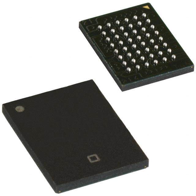
| 产品图片 |
|
| rohs | 否含铅 / 不符合限制有害物质指令(RoHS)规范要求 |
| 产品系列 | 内存,静态随机存取存储器,Cypress Semiconductor CY62167DV30LL-55BVIMoBL® |
| 数据手册 | http://www.cypress.com/?docID=46920 |
| 产品型号 | CY62167DV30LL-55BVI |
| PCN组件/产地 | http://www.cypress.com/?docID=49128 |
| 产品种类 | 静态随机存取存储器 |
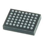
| 供应商器件封装 | 48-VFBGA(8x9.5) |
| 其它名称 | CY62167DV30LL55BVI |
| 包装 | 托盘 |
| 商标 | Cypress Semiconductor |
| 商标名 | MoBL |
| 存储器类型 | SRAM - 异步 |
| 存储容量 | 16 Mbit |
| 存储类型 | SDR |
| 安装风格 | SMD/SMT |
| 封装 | Tray |
| 封装/外壳 | 48-VFBGA |
| 封装/箱体 | VFBGA-48 |
| 工作温度 | -40°C ~ 85°C |
| 工厂包装数量 | 210 |
| 接口 | Parallel |
| 最大工作温度 | + 85 C |
| 最大工作电流 | 30 mA |
| 最小工作温度 | - 40 C |
| 标准包装 | 210 |
| 格式-存储器 | RAM |
| 电压-电源 | 2.2 V ~ 3.6 V |
| 电源电压-最大 | 3.6 V |
| 电源电压-最小 | 2.2 V |
| 类型 | Asynchronous |
| 系列 | CY62167DV30LL |
| 组织 | 1 M x 16 |
| 访问时间 | 55 ns |
| 速度 | 55ns |


_renders/IS61WV102416BLL-10TLI.jpg)


- 商务部:美国ITC正式对集成电路等产品启动337调查
- 曝三星4nm工艺存在良率问题 高通将骁龙8 Gen1或转产台积电
- 太阳诱电将投资9.5亿元在常州建新厂生产MLCC 预计2023年完工
- 英特尔发布欧洲新工厂建设计划 深化IDM 2.0 战略
- 台积电先进制程称霸业界 有大客户加持明年业绩稳了
- 达到5530亿美元!SIA预计今年全球半导体销售额将创下新高
- 英特尔拟将自动驾驶子公司Mobileye上市 估值或超500亿美元
- 三星加码芯片和SET,合并消费电子和移动部门,撤换高东真等 CEO
- 三星电子宣布重大人事变动 还合并消费电子和移动部门
- 海关总署:前11个月进口集成电路产品价值2.52万亿元 增长14.8%


_renders/IS66WVE4M16EBLL-70BLI.jpg)
PDF Datasheet 数据手册内容提取
® CY62167DV30 MoBL 16-Mbit (1 M × 16) Static RAM 16-Mbit (1 M × 16) Static RAM Features automatic power-down feature that significantly reduces power consumption by 99% when addresses are not toggling. The ■Thin small outline package (TSOP-I) configurable as device can also be put into standby mode when deselected (CE1 1 M × 16 or as 2 M × 8 SRAM HIGH or CE2 LOW or both BHE and BLE are HIGH). The input/output pins (I/O through I/O ) are placed in a 0 15 ■Wide voltage range: 2.2 V–3.6 V high-impedance state when: deselected (CE HIGH or CE 1 2 ■Ultra-low active power: LOW), outputs are disabled (OE HIGH), both Byte High Enable Typical active current: 2 mA at f = 1 MHz and Byte Low Enable are disabled (BHE, BLE HIGH), or during a Write operation (CE LOW, CE HIGH and WE LOW). 1 2 ■Ultra-low standby power Writing to the device is accomplished by taking Chip Enables ■Easy memory expansion with CE1, CE2 and OE features (CE1 LOW and CE2 HIGH) and Write Enable (WE) input LOW. If Byte Low Enable (BLE) is LOW, then data from I/O pins (I/O 0 ■Automatic power-down when deselected through I/O ), is written into the location specified on the address 7 ■Complementary metal oxide semiconductor (CMOS) for pins (A0 through A19). If Byte High Enable (BHE) is LOW, then optimum speed / power data from I/O pins (I/O8 through I/O15) is written into the location specified on the address pins (A through A ). 0 19 ■Available in Pb-free and non Pb-free 48-ball very fine-pitch ball Reading from the device is accomplished by taking Chip Enables grid array (VFBGA) and 48-pin TSOP I package (CE LOW and CE HIGH) and Output Enable (OE) LOW while 1 2 forcing the Write Enable (WE) HIGH. If Byte Low Enable (BLE) Functional Description is LOW, then data from the memory location specified by the address pins appear on I/O to I/O . If Byte High Enable (BHE) 0 7 The CY62167DV30 is a high-performance CMOS static RAM is LOW, then data from memory appear on I/O to I/O . See the 8 15 organized as 1M words by 16-bits. This device features truth table at the back of this data sheet for a complete advanced circuit design to provide ultra-low active current. This description of Read and Write modes. is ideal for providing More Battery Life (MoBL) in portable For a complete list of related documentation, click here. applications such as cellular telephones. The device also has an Logic Block Diagram DATA IN DRIVERS A 10 A 9 R A E S 8 D P A 7 O M AAA 65 W DEC 1M R× A1M6 /A 2rMra yx 8 NSE A I/O0–I/O7 4 A 3 RO SE I/O8–I/O15 A 2 A 1 A 0 COLUMN DECODER BYTE BHE WE CE A11A12A13A14A15A16A17A18A19 CE21 OE BLE Power-Down Circuit BHE CE2 BLE CE1 CypressSemiconductorCorporation • 198 Champion Court • SanJose, CA 95134-1709 • 408-943-2600 Document Number: 38-05328 Rev. *M Revised November 19, 2014
® CY62167DV30 MoBL Contents Product Portfolio ..............................................................3 Ordering Information ......................................................13 Pin Configurations ...........................................................3 Ordering Code Definitions .........................................13 Maximum Ratings .............................................................4 Package Diagrams ..........................................................14 Operating Range ...............................................................4 Acronyms ........................................................................16 Electrical Characteristics .................................................4 Document Conventions .................................................16 Capacitance ......................................................................5 Units of Measure .......................................................16 Thermal Resistance ..........................................................5 Document History Page .................................................17 AC Test Loads and Waveforms .......................................5 Sales, Solutions, and Legal Information ......................18 Data Retention Characteristics .......................................6 Worldwide Sales and Design Support .......................18 Data Retention Waveform ................................................6 Products ....................................................................18 Switching Characteristics ................................................7 PSoC® Solutions ......................................................18 Switching Waveforms ......................................................8 Cypress Developer Community .................................18 Truth Table ......................................................................12 Technical Support .....................................................18 Document Number: 38-05328 Rev. *M Page 2 of 18
® CY62167DV30 MoBL Product Portfolio Power Dissipation VCC Range (V) Speed Operating ICC(mA) Product Standby I (A) (ns) f = 1 MHz f = f SB2 Max Min Typ [1] Max Typ [1] Max Typ [1] Max Typ [1] Max CY62167DV30LL 2.2 3.0 3.6 55 2 4 15 30 2.5 22 70 12 25 Pin Configurations Figure 1. 48-ball VFBGA pinout (Top View) [2, 3] 1 2 3 4 5 6 BLE OE A0 A1 A2 CE2 A I/O8 BHE A3 A4 CE1 I/O0 B I/O9 I/O10 A5 A6 I/O1 I/O2 C VSS I/O11 A17 A7 I/O3 Vcc D VCC I/O12 DNU A16 I/O4 Vss E I/O14 I/O13 A14 A15 I/O5 I/O6 F I/O15 A19 A12 A13 WE I/O7 G A18 A8 A9 A10 A11 DNU H Figure 2. 48-pin TSOP I pinout (Top View) [4] A15 1 48 A16 A14 2 47 BYTE A13 3 46 Vss A12 4 45 I/O15/A20 A11 5 44 I/O7 A10 6 43 I/O14 A9 7 42 I/O6 A8 8 41 I/O13 A19 9 40 I/O5 NC 10 39 I/O12 WE 11 38 I/O4 CE2 12 37 Vcc DNU 13 36 I/O11 BHE 14 35 I/O3 BLE 15 34 I/O10 A18 16 33 I/O2 A17 17 32 I/O9 A7 18 31 I/O1 A6 19 30 I/O8 A5 20 29 I/O0 A4 21 28 OE A3 22 27 Vss A2 23 26 CE1 A1 24 25 A0 Notes 1. Typical values are included for reference only and are not guaranteed or tested. Typical values are measured at VCC = VCC(typ.), TA = 25 °C. 2. NC pins are not connected on the die. 3. DNU pins have to be left floating. 4. The BYTE pin in the 48-TSOP I package has to be tied to VCC to use the device as a 1M X 16 SRAM. The 48-TSOP I package can also be used as a 2 M × 8 SRAM by tying the BYTE signal to VSS. In the 2 M × 8 configuration, Pin 45 is A20, while BHE, BLE and I/O8 to I/O14 pins are not used (DNU). Document Number: 38-05328 Rev. *M Page 3 of 18
® CY62167DV30 MoBL Maximum Ratings Static discharge voltage (per MIL-STD-883, Method 3015) ......................... > 2001 V Exceeding maximum ratings may shorten the useful life of the Latch-up current ....................................................> 200 mA device. User guidelines are not tested. Storage temperature ................................–65 °C to +150 °C Operating Range Ambient temperature with power applied ..........................................–55 °C to +125 °C Device Range Ambient V [7] Temperature CC Supply voltage to ground potential .....–0.2 V to V + 0.3 V CC CY62167DV30LL Industrial –40 °C to +85 °C 2.20 V to DC voltage applied to outputs 3.60 V in High-Z state [5, 6] .............................–0.2 V to V + 0.3 V CC DC input voltage [5, 6] ..........................–0.2 V to V + 0.3 V CC Output current into outputs (LOW) .............................20 mA Electrical Characteristics Over the Operating Range CY62167DV30-55 CY62167DV30-70 Parameter Description Test Conditions Unit Min Typ [8] Max Min Typ [8] Max V Output HIGH voltage I = –0.1 mA V = 2.20 V 2.0 – – 2.0 – – V OH OH CC I = –1.0 mA V = 2.70 V 2.4 2.4 OH CC V Output LOW voltage I = 0.1 mA V = 2.20 V – – 0.4 – 0.4 V OL OL CC I = 2.1 mA V = 2.70 V OL CC V Input HIGH voltage V = 2.2 V to 2.7 V 1.8 – V + 0.3 1.8 – V + 0.3 V IH CC CC CC V = 2.7 V to 3.6 V 2.2 2.2 CC V Input LOW voltage V = 2.2 V to 2.7 V –0.3 – 0.6 –0.3 – 0.6 V IL CC V = 2.7 V to 3.6 V 0.8 0.8 CC I Input leakage current GND V V –1 – +1 –1 – +1 A IX I CC I Output leakage current GND V V , output –1 – +1 –1 – +1 A OZ O CC disabled I V operating supply V = V f = f = 1/t – 15 30 – 12 25 mA CC CC CC CC(max) Max RC current I = 0 mA OUT f = 1 MHz 2 4 2 4 CMOS levels ISB1 Automatic power-down CE1 VCC 0.2 V or CE2 0.2 V, – 2.5 22 – 2.5 22 A current – CMOS inputs V V – 0.2 V, V 0.2 V, IN CC IN f = f (address and data only), Max f = 0 (OE, WE), V = 3.60 V CC ISB2 Automatic power-down CE1 VCC – 0.2 V or – 2.5 22 – 2.5 22 A current – CMOS Inputs CE 0.2 V 2 V V – 0.2 V or V 0.2V, IN CC IN f = 0, V = 3.60 V CC Notes 5. VIL(min.) = –2.0 V for pulse durations less than 20 ns. 6. VIH(max) = VCC + 0.75 V for pulse durations less than 20 ns. 7. Full Device AC operation requires linear VCC ramp from 0 to VCC(min.) and VCC must be stable at VCC(min) for 500s. 8. Typical values are included for reference only and are not guaranteed or tested. Typical values are measured at VCC = VCC(typ), TA = 25 °C. Document Number: 38-05328 Rev. *M Page 4 of 18
® CY62167DV30 MoBL Capacitance Parameter [10] Description Test Conditions Max Unit C Input capacitance T = 25 °C, f = 1 MHz, V = V 8 pF IN A CC CC(typ) C Output capacitance 10 pF OUT Thermal Resistance Parameter [10] Description Test Conditions VFBGA TSOP I Unit Thermal resistance Still air, soldered on a 3 × 4.5 inch, 2-layer 55 60 C/W JA (junction to ambient) printed circuit board Thermal resistance 16 4.3 C/W JC (junction to case) AC Test Loads and Waveforms Figure 3. AC Test Loads and Waveforms R1 V ALL INPUT PULSES CC V OUTPUT CC 90% 90% 10% 10% 50 pF[12] R2 GND Rise Time = 1 V/ns Fall Time = 1 V/ns INCLUDING JIG AND SCOPE Equivalentto: THEV ENINEQUIVALENT R TH OUTPUT V Parameters 2.5 V 3.0 V Unit R1 16667 1103 R2 15385 1554 R 8000 645 TH V 1.20 1.75 V TH Document Number: 38-05328 Rev. *M Page 5 of 18
® CY62167DV30 MoBL Data Retention Characteristics Over the Operating Range Parameter Description Conditions Min Typ [9] Max Unit V V for data retention 1.5 – – V DR CC I Data retention current V = 1.5 V, – – 10 A CCDR CC CE V – 0.2 V or CE 0.2 V, 1 CC 2 V V – 0.2 V or V 0.2 V IN CC IN t [10] Chip deselect to data retention 0 – – ns CDR time t [11] Operation recovery time CY62167DV30LL-55 55 – – ns R CY62167DV30LL-70 70 Data Retention Waveform Figure 4. Data Retention Waveform [12] DATA RETENTION MODE VCC VCC, min. VDR 1.5 V VCC, min. tCDR tR CE1 or BHE,BLE or CE2 Notes 9. Typical values are included for reference only and are not guaranteed or tested. Typical values are measured at VCC = VCC(typ), TA = 25 °C. 10.Tested initially and after any design or process changes that may affect these parameters. 11.Full device operation requires linear VCC ramp from VDR to VCC(min.) 100 s or stable at VCC(min.) 100 s. 12.BHE.BLE is the AND of both BHE and BLE. Chip can be deselected by either disabling the chip enable signals or by disabling both BHE and BLE. Document Number: 38-05328 Rev. *M Page 6 of 18
® CY62167DV30 MoBL Switching Characteristics Over the Operating Range 55 ns 70 ns Parameter [13] Description Unit Min Max Min Max Read Cycle t Read cycle time 55 – 70 – ns RC t Address to data valid – 55 – 70 ns AA t Data hold from address change 10 – 10 – ns OHA t CE LOW and CE HIGH to data valid – 55 – 70 ns ACE 1 2 t OE LOW to data valid – 25 – 35 ns DOE t OE LOW to low Z [14] 5 – 5 – ns LZOE t OE HIGH to high Z [14, 15] – 20 – 25 ns HZOE t CE LOW and CE HIGH to low Z [14] 10 – 10 – ns LZCE 1 2 t CE HIGH and CE LOW to high Z [14, 15] – 20 – 25 ns HZCE 1 2 t CE LOW and CE HIGH to power-up 0 – 0 – ns PU 1 2 t CE HIGH and CE LOW to power-down – 55 – 70 ns PD 1 2 t BLE/BHE LOW to data valid – 55 – 70 ns DBE t BLE/BHE LOW to low Z [14] 10 – 10 – ns LZBE t BLE/BHE HIGH to high Z [14, 15] – 20 – 25 ns HZBE Write Cycle [16] t Write cycle time 55 – 70 – ns WC t CE LOW and CE HIGHto write end 40 – 60 – ns SCE 1 2 t Address setup to write end 40 – 60 – ns AW t Address hold from write end 0 – 0 – ns HA t Address setup to write start 0 – 0 – ns SA t WE pulse width 40 – 45 – ns PWE t BLE/BHE LOW to write end 40 – 60 – ns BW t Data setup to write end 25 – 30 – ns SD t Data hold from write end 0 – 0 – ns HD t WE LOW to high-Z [14, 15] – 20 – 25 ns HZWE t WE HIGH to low-Z [14] 10 – 10 – ns LZWE Notes 13.Test conditions for all parameters other than Tri-state parameters assume signal transition time of 1 ns/V, timing reference levels of VCC(typ)/2, input pulse levels of 0 to VCC(typ.), and output loading of the specified IOL/IOH as shown in the “AC Test Loads and Waveforms” section. 14.At any temperature and voltage condition, tHZCE is less than tLZCE, tHZBE is less than tLZBE, tHZOE is less than tLZOE, and tHZWE is less than tLZWE for any device. 15.tHZOE, tHZCE, tHZBE, and tHZWE transitions are measured when the outputs enter a high impedance state. 16.The internal Write time of the memory is defined by the overlap of WE, CE1 = VIL, BHE and/or BLE = VIL, and CE2 = VIH. All signals must be ACTIVE to initiate a write and any of these signals can terminate a write by going INACTIVE. The data input setup and hold timing should be referenced to the edge of the signal that terminates the Write. Document Number: 38-05328 Rev. *M Page 7 of 18
® CY62167DV30 MoBL Switching Waveforms Figure 5. Read Cycle 1 (Address Transition Controlled) [17, 18] t RC ADDRESS t AA t OHA DATA OUT PREVIOUS DATA VALID DATA VALID Figure 6. Read Cycle 2 (OE Controlled) [18, 19] ADDRESS CE1 tRC t PD t HZCE CE2 t ACE BHE/BLE t DBE t t HZBE LZBE OE t t HZOE DOE t HIGH LZOE HIGH IMPEDANCE IMPEDANCE DATA OUT DATA VALID t LZCE VCC tPU ICC SUPPLY 50% 50% I CURRENT SB Notes 17.The device is continuously selected. OE, CE1 = VIL, BHE and/or BLE = VIL, and CE2 = VIH. 18.WE is HIGH for read cycle. 19.Address valid prior to or coincident with CE1, BHE, BLE transition LOW and CE2 transition HIGH. Document Number: 38-05328 Rev. *M Page 8 of 18
® CY62167DV30 MoBL Switching Waveforms (continued) Figure 7. Write Cycle 1 (WE Controlled) [20, 21, 22] t WC ADDRESS t SCE CE 1 CE 2 t t AW HA t t SA PWE WE t BHE/BLE BW OE t t SD HD DATAI/O See Note 23 VALID DATA t HZOE Notes 20.The internal Write time of the memory is defined by the overlap of WE, CE1 = VIL, BHE and/or BLE = VIL, and CE2 = VIH. All signals must be ACTIVE to initiate a write and any of these signals can terminate a write by going INACTIVE. The data input setup and hold timing should be referenced to the edge of the signal that terminates the Write. 21.Data I/O is high-impedance if OE = VIH. 22.If CE1 goes HIGH and CE2 goes LOW simultaneously with WE = VIH, the output remains in a high-impedance state. 23.During this period, the I/Os are in output state and input signals should not be applied. Document Number: 38-05328 Rev. *M Page 9 of 18
® CY62167DV30 MoBL Switching Waveforms (continued) Figure 8. Write Cycle 2 (CE or CE Controlled) [24, 25, 26] 1 2 t WC ADDRESS t SCE CE 1 CE 2 t SA t t AW HA t PWE WE t BHE/BLE BW OE t t SD HD DATAI/O Note 27 VALID DATA t HZOE Figure 9. Write Cycle 3 (WE Controlled, OE LOW) [26] t WC ADDRESS t SCE CE 1 CE 2 t BHE/BLE BW t t AW HA t t SA PWE WE t t SD HD DATA I/O Note 27 VALID DATA tHZWE tLZWE Notes 24.The internal Write time of the memory is defined by the overlap of WE, CE1 = VIL, BHE and/or BLE = VIL, and CE2 = VIH. All signals must be ACTIVE to initiate a write and any of these signals can terminate a write by going INACTIVE. The data input setup and hold timing should be referenced to the edge of the signal that terminates the Write. 25.Data I/O is high-impedance if OE = VIH. 26.If CE1 goes HIGH and CE2 goes LOW simultaneously with WE = VIH, the output remains in a high-impedance state. 27.During this period, the I/Os are in output state and input signals should not be applied. Document Number: 38-05328 Rev. *M Page 10 of 18
® CY62167DV30 MoBL Switching Waveforms (continued) Figure 10. Write Cycle 4 (BHE/BLE Controlled, OE LOW) [28] t WC ADDRESS CE 1 CE 2 t SCE t t AW HA t BW BHE/BLE t SA t WE PWE t t SD HD DATA I/O Note 29 VALID DATA Notes 28.If CE1 goes HIGH and CE2 goes LOW simultaneously with WE = VIH, the output remains in a high-impedance state. 29.During this period, the I/Os are in output state and input signals should not be applied. Document Number: 38-05328 Rev. *M Page 11 of 18
® CY62167DV30 MoBL Truth Table CE CE WE OE BHE BLE Inputs/Outputs Mode Power 1 2 H X X X X X High Z Deselect/Power-down Standby (I ) SB X L X X X X High Z Deselect/Power-down Standby (I ) SB X X X X H H High Z Deselect/Power-down Standby (I ) SB L H H L L L Data out (I/O –I/O ) Read Active (I ) 0 15 CC L H H L H L High Z (I/O –I/O ); Read Active (I ) 8 15 CC Data out (I/O –I/O ) 0 7 L H H L L H Data out (I/O –I/O ); Read Active (I ) 8 15 CC High Z (I/O –I/O ) 0 7 L H L X L L Data in (I/O –I/O ) Write Active (I ) 0 15 CC L H L X H L High Z (I/O –I/O ); Write Active (I ) 8 15 CC Data in (I/O –I/O ) 0 7 L H L X L H Data in (I/O –I/O ); Write Active (I ) 8 15 CC High Z (I/O –I/O ) 0 7 L H H H L H High Z Output disabled Active (I ) CC L H H H H L High Z Output disabled Active (I ) CC L H H H L L High Z Output disabled Active (I ) CC Document Number: 38-05328 Rev. *M Page 12 of 18
® CY62167DV30 MoBL Ordering Information Speed Package Operating Ordering Code Package Type (ns) Diagram Range 55 CY62167DV30LL-55BVI 51-85178 48-ball FBGA (8 × 9.5 × 1 mm) Industrial CY62167DV30LL-55BVXI 48-ball FBGA (8 × 9.5 × 1 mm) Pb-free CY62167DV30LL-55ZXI 51-85183 48-pin TSOP I (12 × 18.4 × 1 mm) Pb-free 70 CY62167DV30LL-70BVI 51-85178 48-ball FBGA (8 × 9.5 × 1 mm) Please contact your local Cypress sales representative for availability of these parts Ordering Code Definitions CY 621 6 7 D V30 LL - XX XX X I Temperature Range: I = Industrial Pb-free Package Type: XX = BV or Z BV = 48-ball FBGA; Z = 48-pin TSOP I Speed Grade: XX = 55 ns or 70 ns Low Power Voltage Range: 3 V Typical Process Technology: 130 nm Technology Bus Width: 7 = × 16 Density: 6 = 16-Mbit Family Code: 621 = MoBL SRAM family Company ID: CY = Cypress Document Number: 38-05328 Rev. *M Page 13 of 18
® CY62167DV30 MoBL Package Diagrams Figure 11. 48-ball VFBGA (8 × 9.5 × 1 mm) BV48B Package Outline, 51-85178 51-85178 *C Document Number: 38-05328 Rev. *M Page 14 of 18
® CY62167DV30 MoBL Package Diagrams (continued) Figure 12. 48-pin TSOP I (12 × 18.4 × 1 mm) Z48A Package Outline, 51-85183 51-85183 *C Document Number: 38-05328 Rev. *M Page 15 of 18
® CY62167DV30 MoBL Acronyms Document Conventions Acronym Description Units of Measure CMOS Complementary Metal Oxide Semiconductor Symbol Unit of Measure I/O Input/Output °C degrees Celsius SRAM Static Random Access Memory MHz megahertz TSOP Thin Small Outline Package A microampere VFBGA Very Fine-Pitch Ball Grid Array mA milliampere ns nanosecond ohm pF picofarad V volt W watt Document Number: 38-05328 Rev. *M Page 16 of 18
® CY62167DV30 MoBL Document History Page Document Title: CY62167DV30 MoBL®, 16-Mbit (1 M × 16) Static RAM Document Number: 38-05328 Orig. of Submission Revision ECN Description of Change Change Date ** 118408 GUG 09/30/02 New data sheet. *A 123692 DPM 02/11/03 Changed status from Advanced to Preliminary. Added package diagram *B 126555 DPM 04/25/03 Minor change: Changed Sunset Owner from DPM to HRT *C 127841 XRJ 09/10/03 Added 48 TSOP I package *D 205701 AJU See ECN Changed BYTE pin usage description for 48 TSOPI package *E 238050 KKV/AJU See ECN Replaced 48-ball VFBGA package diagram; Modified Package Name in Ordering Information table from BV48A to BV48B *F 304054 PCI See ECN Added 45-ns Speed Bin in AC, DC and Ordering Information tables Added Footnote #12 on page #4 Added Pb-free packages on page # 10 *G 492895 VKN See ECN Modified datasheet to explain x8 configurability. Removed L power bin from the product offering Updated Ordering Information Table *H 2896036 AJU 03/19/10 Removed 45-ns. Removed inactive parts from Ordering Information. Updated Packaging Information Updated links in Sales, Solutions, and Legal Information. *I 3067267 RAME 11/08/10 Updated datasheet as per new template Added Ordering Code Definitions. Added Acronyms and Units of Measure. Updated all table notes to footnote. Package diagram updated 51-85178 from ** to *A *J 3329789 RAME 07/27/11 Removed references to AN1064 SRAM system guidelines. Updated template according to current CY standards. *K 4108382 AJU 08/29/2013 Updated Pin Configurations: Removed the note “Ball H6 for the FBGA package can be used to upgrade to a 32M density” and its reference in Figure1. Updated Package Diagrams: spec 51-85178 – Changed revision from *A to *C. Updated in new template. *L 4192919 VINI 11/15/2013 No technical updates. Completing Sunset Review. *M 4574377 VINI 11/19/2014 Added related documentation hyperlink in page 1. Document Number: 38-05328 Rev. *M Page 17 of 18
® CY62167DV30 MoBL Sales, Solutions, and Legal Information Worldwide Sales and Design Support Cypress maintains a worldwide network of offices, solution centers, manufacturer’s representatives, and distributors. To find the office closest to you, visit us at Cypress Locations. Products PSoC® Solutions Automotive cypress.com/go/automotive psoc.cypress.com/solutions Clocks & Buffers cypress.com/go/clocks PSoC 1 | PSoC 3 | PSoC 4 | PSoC 5LP Interface cypress.com/go/interface Cypress Developer Community Lighting & Power Control cypress.com/go/powerpsoc Community | Forums | Blogs | Video | Training cypress.com/go/plc Technical Support Memory cypress.com/go/memory cypress.com/go/support PSoC cypress.com/go/psoc Touch Sensing cypress.com/go/touch USB Controllers cypress.com/go/USB Wireless/RF cypress.com/go/wireless © Cypress Semiconductor Corporation, 2002-2014. The information contained herein is subject to change without notice. Cypress Semiconductor Corporation assumes no responsibility for the use of any circuitry other than circuitry embodied in a Cypress product. Nor does it convey or imply any license under patent or other rights. Cypress products are not warranted nor intended to be used for medical, life support, life saving, critical control or safety applications, unless pursuant to an express written agreement with Cypress. Furthermore, Cypress does not authorize its products for use as critical components in life-support systems where a malfunction or failure may reasonably be expected to result in significant injury to the user. The inclusion of Cypress products in life-support systems application implies that the manufacturer assumes all risk of such use and in doing so indemnifies Cypress against all charges. Any Source Code (software and/or firmware) is owned by Cypress Semiconductor Corporation (Cypress) and is protected by and subject to worldwide patent protection (United States and foreign), United States copyright laws and international treaty provisions. Cypress hereby grants to licensee a personal, non-exclusive, non-transferable license to copy, use, modify, create derivative works of, and compile the Cypress Source Code and derivative works for the sole purpose of creating custom software and or firmware in support of licensee product to be used only in conjunction with a Cypress integrated circuit as specified in the applicable agreement. Any reproduction, modification, translation, compilation, or representation of this Source Code except as specified above is prohibited without the express written permission of Cypress. Disclaimer: CYPRESS MAKES NO WARRANTY OF ANY KIND, EXPRESS OR IMPLIED, WITH REGARD TO THIS MATERIAL, INCLUDING, BUT NOT LIMITED TO, THE IMPLIED WARRANTIES OF MERCHANTABILITY AND FITNESS FOR A PARTICULAR PURPOSE. Cypress reserves the right to make changes without further notice to the materials described herein. Cypress does not assume any liability arising out of the application or use of any product or circuit described herein. Cypress does not authorize its products for use as critical components in life-support systems where a malfunction or failure may reasonably be expected to result in significant injury to the user. The inclusion of Cypress’ product in a life-support systems application implies that the manufacturer assumes all risk of such use and in doing so indemnifies Cypress against all charges. Use may be limited by and subject to the applicable Cypress software license agreement. Document Number: 38-05328 Rev. *M Revised November 19, 2014 Page 18 of 18 MoBL is a registered trademark and More Battery Life is a trademark of Cypress Semiconductor Corporation. All product and company names mentioned in this document may be the trademarks of their respective holders.
Mouser Electronics Authorized Distributor Click to View Pricing, Inventory, Delivery & Lifecycle Information: C ypress Semiconductor: CY62167DV30LL-55BVI CY62167DV30LL-55BVIT CY62167DV30LL-55BVXI CY62167DV30LL-55BVXIT CY62167DV30LL-55ZXI CY62167DV30LL-55ZXIT CY62167DV30LL-70BVI CY62167DV30LL-70BVIT