
 Datasheet下载
- 型号: CY14B101J2-SXI
- 制造商: Cypress Semiconductor
- 库位|库存: xxxx|xxxx
- 要求:
| 数量阶梯 | 香港交货 | 国内含税 |
| +xxxx | $xxxx | ¥xxxx |
查看当月历史价格
查看今年历史价格
CY14B101J2-SXI产品简介:
ICGOO电子元器件商城为您提供CY14B101J2-SXI由Cypress Semiconductor设计生产,在icgoo商城现货销售,并且可以通过原厂、代理商等渠道进行代购。 CY14B101J2-SXI价格参考¥25.28-¥25.64。Cypress SemiconductorCY14B101J2-SXI封装/规格:存储器, NVSRAM(非易失性 SRAM) 存储器 IC 1Mb (128K x 8) I²C 3.4MHz 8-SOIC。您可以下载CY14B101J2-SXI参考资料、Datasheet数据手册功能说明书,资料中有CY14B101J2-SXI 详细功能的应用电路图电压和使用方法及教程。
Cypress Semiconductor Corp的CY14B101J2-SXI是一款非易失性存储器(NVRAM)产品,结合了SRAM和非易失性存储技术的优点,适用于需要高速访问和数据持久性的应用场景。该器件常用于工业控制、通信设备、医疗仪器、汽车电子等领域,例如在断电情况下需保留关键数据的系统、实时数据记录、固件存储以及需要高可靠性和高耐久性的嵌入式系统中。此外,它也可用于网络设备中的配置存储和日志记录等功能。
| 参数 | 数值 |
| 产品目录 | 集成电路 (IC)半导体 |
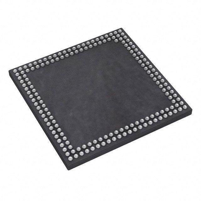
| 描述 | IC NVSRAM 1MBIT 3.4MHZ 8SOICNVRAM 1Mb 3V 3.4Mhz 128K x 8 SPI nvSRAM |
| 产品分类 | |
| 品牌 | Cypress Semiconductor |
| 产品手册 | |
| 产品图片 |
|
| rohs | 符合RoHS无铅 / 符合限制有害物质指令(RoHS)规范要求 |
| 产品系列 | 内存,NVRAM,Cypress Semiconductor CY14B101J2-SXI- |
| 数据手册 | http://www.cypress.com/?docID=46794 |
| 产品型号 | CY14B101J2-SXI |
| PCN组件/产地 | http://www.cypress.com/?docID=44762http://www.cypress.com/?docID=48110 |
| 产品种类 | NVRAM |
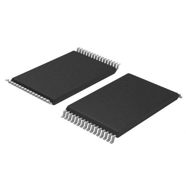
| 供应商器件封装 | 8-SOIC |
| 其它名称 | CY14B101J2SXI |
| 包装 | 管件 |
| 商标 | Cypress Semiconductor |
| 存储器类型 | NVSRAM(非易失 SRAM) |
| 存储容量 | 1M (128K x 8) |
| 封装 | Tube |
| 封装/外壳 | 8-SOIC(0.154",3.90mm 宽) |
| 工作温度 | -40°C ~ 85°C |
| 工厂包装数量 | 194 |
| 接口 | I²C,2 线串口 |
| 标准包装 | 194 |
| 格式-存储器 | RAM |
| 电压-电源 | 2.7 V ~ 3.6 V |
| 系列 | CY14B101J2 |
| 速度 | 3.4MHz |


- 商务部:美国ITC正式对集成电路等产品启动337调查
- 曝三星4nm工艺存在良率问题 高通将骁龙8 Gen1或转产台积电
- 太阳诱电将投资9.5亿元在常州建新厂生产MLCC 预计2023年完工
- 英特尔发布欧洲新工厂建设计划 深化IDM 2.0 战略
- 台积电先进制程称霸业界 有大客户加持明年业绩稳了
- 达到5530亿美元!SIA预计今年全球半导体销售额将创下新高
- 英特尔拟将自动驾驶子公司Mobileye上市 估值或超500亿美元
- 三星加码芯片和SET,合并消费电子和移动部门,撤换高东真等 CEO
- 三星电子宣布重大人事变动 还合并消费电子和移动部门
- 海关总署:前11个月进口集成电路产品价值2.52万亿元 增长14.8%
_renders/IS43DR81280C-25DBLI.jpg)


_renders/IS45S16100H-7BLA1.jpg)
PDF Datasheet 数据手册内容提取
CY14C101J CY14B101J CY14E101J 2 1-Mbit (128K × 8) Serial (I C) nvSRAM 1-Mbit (128K × 8) Serial (I2C) nvSRAM Features ❐Sleep mode current of 8 µA ■Industry standard configurations ■1-Mbit nonvolatile static random access memory (nvSRAM) ❐Operating voltages: ❐Internally organized as 128K × 8 • CY14C101J: V = 2.4 V to 2.6 V ❐STORE to QuantumTrap nonvolatile elements initiated CC automatically on power-down (AutoStore) or by using I2C • CY14B101J: VCC = 2.7 V to 3.6 V • CY14E101J: V = 4.5 V to 5.5 V command (Software STORE) or HSB pin (Hardware STORE) CC ❐Industrial temperature ❐RECALL to SRAM initiated on power-up (Power-Up RECALL) or by I2C command (Software RECALL) ❐8- and 16-pin small outline integrated circuit (SOIC) package ❐Automatic STORE on power-down with a small capacitor ❐Restriction of hazardous substances (RoHS) compliant (except for CY14X101J1) Functional Description ■High reliability ❐Infinite read, write, and RECALL cycles The Cypress CY14C101J/CY14B101J/CY14E101J combines a 1-Mbit nvSRAM[2] with a nonvolatile element in each memory ❐1 million STORE cycles to QuantumTrap cell. The memory is organized as 128K words of 8 bits each. The ❐Data retention: 20 years at 85 °C embedded nonvolatile elements incorporate the QuantumTrap ■High speed I2C interface[1] technology, creating the world’s most reliable nonvolatile ❐Industry standard 100 kHz and 400 kHz speed memory. The SRAM provides infinite read and write cycles, while ❐Fast-mode Plus: 1 MHz speed the QuantumTrap cells provide highly reliable nonvolatile storage of data. Data transfers from SRAM to the nonvolatile ❐High speed: 3.4 MHz elements (STORE operation) takes place automatically at ❐Zero cycle delay reads and writes power-down (except for CY14X101J1). On power-up, data is ■Write protection restored to the SRAM from the nonvolatile memory (RECALL ❐Hardware protection using Write Protect (WP) pin operation). The STORE and RECALL operations can also be ❐Software block protection for 1/4, 1/2, or entire array initiated by the user through I2C commands. ■I2C access to special functions For a complete list of related documentation, click here. ❐Nonvolatile STORE/RECALL Configuration ❐8 byte serial number ❐Manufacturer ID and Product ID Feature CY14X101J1 CY14X101J2 CY14X101J3 ❐Sleep mode AutoStore No Yes Yes ■Low power consumption Software STORE Yes Yes Yes ❐Average active current of 1 mA at 3.4 MHz operation Hardware STORE No No Yes ❐Average standby mode current of 150 µA Logic Block Diagram Serial Number 8 x 8 VCC VCAP Manufacturer ID / Product ID Power Control Memory Control Register Block Command Register Quantum Trap 128 K x 8 Sleep SSDCAL I 2C Control Logic ControMl Reemgoisryte Srsla Svleave Memory 1S28R AKM x 8 STROERCEALL Slave Address Address and Data A2, A1 Decoder Control WP Notes 1. The I2C nvSRAM is a single solution which is usable for all four speed modes of operation. As a result, some I/O parameters are slightly different than those on chips which support only one mode of operation. Refer to AN87209 for more details. 2. Serial (I2C) nvSRAM is referred to as nvSRAM throughout the datasheet. CypressSemiconductorCorporation • 198 Champion Court • SanJose, CA 95134-1709 • 408-943-2600 Document Number: 001-54050 Rev. *P Revised August 7, 2018
CY14C101J CY14B101J CY14E101J Contents Pinouts ..............................................................................3 Maximum Ratings ...........................................................18 Pin Definitions ..................................................................3 Operating Range .............................................................18 I2C Interface ......................................................................4 DC Electrical Characteristics ........................................18 Protocol Overview ............................................................4 Data Retention and Endurance .....................................20 I2C Protocol – Data Transfer .......................................4 Thermal Resistance ........................................................20 Data Validity ................................................................5 AC Test Loads and Waveforms .....................................20 START Condition (S) ...................................................5 AC Test Conditions ........................................................20 STOP Condition (P) .....................................................5 AC Switching Characteristics .......................................21 Repeated START (Sr) .................................................5 Switching Waveforms ....................................................21 Byte Format .................................................................5 nvSRAM Specifications .................................................22 Acknowledge / No-acknowledge .................................5 Switching Waveforms ....................................................23 High-Speed Mode (Hs-mode) .....................................6 Software Controlled STORE/RECALL Cycles ..............24 Slave Device Address .................................................7 Switching Waveforms ....................................................24 Write Protection (WP) ..................................................9 Hardware STORE Cycle .................................................25 AutoStore Operation ....................................................9 Switching Waveforms ....................................................25 Hardware STORE and HSB pin Operation .................9 Ordering Information ......................................................26 Hardware RECALL (Power-Up) ..................................9 Ordering Code Definitions .........................................26 Write Operation .........................................................10 Package Diagrams ..........................................................27 Read Operation .........................................................10 Acronyms ........................................................................29 Memory Slave Access ...............................................10 Document Conventions .................................................29 Control Registers Slave .............................................14 Units of Measure .......................................................29 Write Control Registers .............................................14 Document History Page .................................................30 Serial Number .................................................................16 Sales, Solutions, and Legal Information ......................33 Serial Number Write ..................................................16 Worldwide Sales and Design Support .......................33 Serial Number Lock ...................................................16 Products ....................................................................33 Serial Number Read ..................................................16 PSoC® Solutions ......................................................33 Device ID .........................................................................17 Cypress Developer Community .................................33 Executing Commands Using Command Register .....17 Technical Support .....................................................33 Document Number: 001-54050 Rev. *P Page 2 of 33
CY14C101J CY14B101J CY14E101J Pinouts Figure 1. 8-pin SOIC pinout [3] NC 1 8 VCC VCAP 1 8 VCC A1 2 CY14X101J1 7 WP A1 2 CY14X101J2 7 WP Top View Top View A2 3 6 SCL A2 3 6 SCL not to scale not to scale VSS 4 5 SDA V SS 4 5 SDA Figure 2. 16-pin SOIC pinout NC 1 16 VCC NC 2 15 NC NC 3 CY14X101J3 14 VCAP NC 4 Top View 13 A2 not to scale WP 5 12 SDA [3] NC 6 11 SCL NC 7 10 A1 VSS 8 9 HSB Pin Definitions Pin Name I/O Type Description SCL Input Clock. Runs at speeds up to a maximum of f . SCL SDA Input/Output I/O. Input/Output of data through I2C interface. Output: Is open-drain and requires an external pull-up resistor. WP Input Write Protect. Protects the memory from all writes. This pin is internally pulled LOW and hence can be left open if not connected. A2–A1 Input Slave Address. Defines the slave address for I2C. This pin is internally pulled LOW and hence can be left open if not connected. HSB Input/Output Hardware STORE Busy Output: Indicates busy status of nvSRAM when LOW. After each Hardware and Software STORE operation HSB is driven HIGH for a short time (t ) with standard output high current and then a weak HHHD internal pull-up resistor keeps this pin HIGH (External pull up resistor connection optional). Input: Hardware STORE implemented by pulling this pin LOW externally. V Power supply AutoStore capacitor. Supplies power to the nvSRAM during power loss to STORE data from the SRAM CAP to nonvolatile elements. If not required, AutoStore must be disabled and this pin left as no connect. It must never be connected to ground. NC No connect No connect. This pin is not connected to the die. V Power supply Ground. SS V Power supply Power supply. CC Note 3. This pin is reserved for lower densities. Document Number: 001-54050 Rev. *P Page 3 of 33
CY14C101J CY14B101J CY14E101J I2C Interface bit slave address and eighth bit (R/W) indicating a read (1) or a write (0) operation. All signals are transmitted on the open-drain I2C bus consists of two lines – serial clock line (SCL) and serial SDA line and are synchronized with the clock on SCL line. Each data line (SDA) that carry information between multiple devices byte of data transmitted on the I2C bus is acknowledged by the on the bus. I2C supports multi-master and multi-slave receiver by holding the SDA line LOW on the ninth clock pulse. configurations. The data is transmitted from the transmitter to the The request for write by the master is followed by the memory receiver on the SDA line and is synchronized with the clock SCL address and data bytes on the SDA line. The writes can be generated by the master. performed in burst-mode by sending multiple bytes of data. The memory address increments automatically after receiving The SCL and SDA lines are open-drain lines and are pulled up /transmitting of each byte on the falling edge of 9th clock cycle. to V using resistors. The choice of a pull-up resistor on the CC The new address is latched just prior to sending/receiving the system depends on the bus capacitance and the intended speed acknowledgment bit. This allows the next sequential byte to be of operation. The master generates the clock and all the data accessed with no additional addressing. On reaching the last I/Os are transmitted in synchronization with this clock. The memory location, the address rolls back to 0x00000 and writes CY14X101J supports up to 3.4 MHz clock speed on SCL line. continue. The slave responds to each byte sent by the master Protocol Overview during a write operation with an ACK. A write sequence can be terminated by the master generating a STOP or Repeated START condition. This device supports only a 7-bit addressable scheme. The master generates a START condition to initiate the A read request is performed at the current address location communication followed by broadcasting a slave select byte. (address next to the last location accessed for read or write). The The slave select byte consists of a seven bit address of the slave memory slave device responds to a read request by transmitting that the master intends to communicate with and R/W bit the data on the current address location to the master. A random indicating a read or a write operation. The selected slave address read may also be performed by first sending a write responds to this with an acknowledgement (ACK). After a slave request with the intended address of read. The master must is selected, the remaining part of the communication takes place abort the write immediately after the last address byte and issue between the master and the selected slave device. The other a Repeated START or STOP signal to prevent any write devices on the bus ignore the signals on the SDA line till a STOP operation. The following read operation starts from this address. or Repeated START condition is detected. The data transfer is The master acknowledges the receipt of one byte of data by done between the master and the selected slave device through holding the SDA pin LOW for the ninth clock pulse. The reads the SDA pin synchronized with the SCL clock generated by the can be terminated by the master sending a no-acknowledge master. (NACK) signal on the SDA line after the last data byte. The no-acknowledge signal causes the CY14X101J to release the I2C Protocol – Data Transfer SDA line and the master can then generate a STOP or a Each transaction in I2C protocol starts with the master Repeated START condition to initiate a new operation. generating a START condition on the bus, followed by a seven Figure 3. System Configuration using Serial (I2C) nvSRAM Vcc R = (V - V max) / I Pmin CC OL OL R = t / (0.8473 * C ) Pmax r b SDA Microcontroller SCL Vcc Vcc A1 SCL A1 SCL A1 SCL A2 SDA A2 SDA A2 SDA WP WP WP CY14X101J CY14X101J CY14X101J #0 #1 #3 Document Number: 001-54050 Rev. *P Page 4 of 33
CY14C101J CY14B101J CY14E101J Data Validity STOP Condition (P) The data on the SDA line must be stable during the HIGH period A LOW to HIGH transition on the SDA line while SCL is HIGH of the clock. The state of the data line can only change when the indicates a STOP condition. This condition indicates the end of clock on the SCL line is LOW for the data to be valid. There are the ongoing transaction. only two conditions under which the SDA line may change state START and STOP conditions are always generated by the with SCL line held HIGH, that is, START and STOP condition. master. The bus is considered to be busy after the START The START and STOP conditions are generated by the master condition. The bus is considered to be free again after the STOP to signal the beginning and end of a communication sequence condition. on the I2C bus. Repeated START (Sr) START Condition (S) If an Repeated START condition is generated instead of a STOP A HIGH to LOW transition on the SDA line while SCL is HIGH condition the bus continues to be busy. The ongoing transaction indicates a START condition. Every transaction in I2C begins on the I2C lines is stopped and the bus waits for the master to with the master generating a START condition. send a slave ID for communication to restart. Figure 4. START and STOP Conditions full pagewidth SDA SDA SCL SCL S P START Condition STOP Condition Figure 5. Data Transfer on the I2C Bus handbook, full pagewidth P SDA MSB Acknowledgement Acknowledgement Sr signal from slave signal from receiver SCL S Sr or 1 2 7 8 9 1 2 3 - 8 9 or Sr P ACK ACK START or STOP or Repeated START Byte complete, Clock line held LOW while Repeated START condition interrupt within slave interrupts are serviced condition Byte Format does not acknowledge the receipt of data and the operation is Each operation in I2C is done using 8 bit words. The bits are sent aborted. NACK can be generated by master during a READ operation in in MSB first format on SDA line and each byte is followed by an ACK signal by the receiver. following cases: An operation continues till a NACK is sent by the receiver or ■The master did not receive valid data due to noise STOP or Repeated START condition is generated by the master ■The master generates a NACK to abort the READ sequence. The SDA line must remain stable when the clock (SCL) is HIGH After a NACK is issued by the master, nvSRAM slave releases except for a START or STOP condition. control of the SDA pin and the master is free to generate a Repeated START or STOP condition. Acknowledge / No-acknowledge NACK can be generated by nvSRAM slave during a WRITE After transmitting one byte of data or address, the transmitter operation in following cases: releases the SDA line. The receiver pulls the SDA line LOW to ■nvSRAM did not receive valid data due to noise. acknowledge the receipt of the byte. Every byte of data transferred on the I2C bus needs to be responded with an ACK ■The master tries to access write protected locations on the signal by the receiver to continue the operation. Failing to do so nvSRAM. Master must restart the communication by is considered as a NACK state. NACK is the state where receiver generating a STOP or Repeated START condition. Document Number: 001-54050 Rev. *P Page 5 of 33
CY14C101J CY14B101J CY14E101J Figure 6. Acknowledge on the I2C Bus handbook, full pagewidth DATA OUTPUT BY MASTER not acknowledge (A) DATA OUTPUT BY SLAVE acknowledge (A) SCL FROM 1 2 8 9 MASTER S clock pulse for START acknowledgement condition High-Speed Mode (Hs-mode) Serial Data Format in Hs-mode In Hs-mode, nvSRAM can transfer data at bit rates of up to Serial data transfer format in Hs-mode meets the standard-mode 3.4Mbit/s. A master code (0000 1XXXb) must be issued to place I2C-bus specification. Hs-mode can only commence after the the device into high speed mode. This enables master slave following conditions (all of which are in F/S-modes): communication for speed upto 3.4 MHz. A stop condition exits 1.START condition (S) Hs-mode. 2.8-bit master code (0000 1XXXb) 3.No-acknowledge bit (A) Figure 7. Data transfer format in Hs-mode handbook, full pagewidth F/S-mode Hs-mode F/S-mode S MASTER CODE A Sr SLAVE ADD. R/W A DATA A/A P n (bytes+ ack.) Hs-mode continues Sr SLAVE ADD. Single and multiple-byte reads and writes are supported. After continue data transfer in Hs-mode, the master sends Repeated the device enters into Hs-mode, data transfer continues in START (Sr). Hs-mode until stop condition is sent by master device. The slave See Figure 13 on page 11 and Figure 16 on page 12 for Hs-mode switches back to F/S-mode after a STOP condition (P). To timings for read and write operation. Document Number: 001-54050 Rev. *P Page 6 of 33
CY14C101J CY14B101J CY14E101J Slave Device Address address field for accessing Memory and Control Registers. The Every slave device on an I2C bus has a device select address. accessing mechanism is described in Memory Slave Device. The first byte after START condition contains the slave device The nvSRAM product provides two different functionalities: address with which the master intends to communicate. The Memory and Control Registers functions (such as serial number seven MSBs are the device address and the LSB (R/W bit) is and product ID). The two functions of the device are accessed used for indicating Read or Write operation. The CY14X101J through different slave device addresses. The first four most reserves two sets of upper 4 MSBs [7:4] in the slave device significant bits [7:4] in the device address register are used to select between the nvSRAM functions. Table 1. Slave device Addressing nvSRAM Bit 7 Bit 6 Bit 5 Bit 4 Bit 3 Bit 2 Bit 1 Bit 0 Function Select CY14X101J Slave Devices 1 0 1 0 Device Select ID A16 R/W Selects Memory Memory, 128K × 8 Control Registers - Memory Control Register, 1 × 8 Selects Control - Serial Number, 8 × 8 0 0 1 1 Device Select ID X R/W Registers - Device ID, 4 × 8 - Command Register, 1 × 8 Memory Slave Device The nvSRAM device is selected for Read/Write if the master Figure 9. Control Registers Slave Device Address issues the slave address as 1010b followed by two bits of device MSB LSB select. If slave address sent by the master matches with the handbook, halfpage Memory Slave device address then depending on the R/W bit of 0 0 1 1 A2 A1 X R/W the slave address, data is either read from (R/W = ‘1’) or written to (R/W = ‘0’) the nvSRAM. Slave ID Device The address length for CY14X101J is 17 bits and thus it requires Select 3 address bytes to map the entire memory address location. To save an extra byte for memory addressing, the 17th bit (A16) is Table 2. Control Registers Map mapped to the slave address select bit (A0). The dedicated two address bytes represent bit A0 to A15. Address Description Read/Write Details 0x00 Memory Read/Write Contains Block Control Protect Bits and Serial Figure 8. Memory Slave Device Address Register Number Lock bit MSB LSB handbook, halfpage 0x01 Serial Number Read/Write Programmable Serial 1 0 1 0 A2 A1 A16 R/W 0x02 8 Bytes (Read only Number. Locked by when SNL setting the Serial 0x03 is set) Number lock bit in the Slave ID Device MSB of Select Address 0x04 Memory Control Register to ‘1’. 0x05 Control Registers Slave Device 0x06 The Control Registers Slave device includes the Serial Number, 0x07 Product ID, Memory Control and Command Register. The nvSRAM Control Register Slave device is selected for 0x08 Read/Write if the master issues the Slave address as 0011b 0x09 Device ID Read only Device ID is factory followed by two bits of device select. Then, depending on the programmed 0x0A R/W bit of the Slave address, data is either read from (R/W= ‘1’) or written to (R/W = ‘0’) the device. 0x0B 0x0C Document Number: 001-54050 Rev. *P Page 7 of 33
CY14C101J CY14B101J CY14E101J Table 2. Control Registers Map (continued) Table 5. Command Register Bytes (continued) Address Description Read/Write Details Data Byte Command Description [7:0] 0x0D Reserved Reserved Reserved 0110 0000 RECALL RECALL data from nonvolatile 0xAA Command Write only Allows commands for memory to SRAM Register STORE, RECALL, AutoStore 0101 1001 ASENB Enable AutoStore Enable/Disable, 0001 1001 ASDISB Disable AutoStore SLEEP Mode 1011 1001 SLEEP Enter Sleep Mode for low power consumption Memory Control Register The Memory Control Register contains the following bits: ■STORE: Initiates nvSRAM Software STORE. The nvSRAM cannot be accessed for t time after this instruction has Table 3. Memory Control Register Bits STORE been executed. When initiated, the device performs a STORE Bit 7 Bit 6 Bit 5 Bit 4 Bit 3 Bit 2 Bit 1 Bit 0 operation regardless of whether a write has been performed since the last NV operation. After the t cycle time is 0 SNL 0 0 BP1 BP0 0 0 STORE completed, the SRAM is activated again for read and write (0) (0) (0) operations. ■RECALL: Initiates nvSRAM Software RECALL. The nvSRAM ■BP1:BP0: Block Protect bits are used to protect 1/4, 1/2 or full cannot be accessed for t time after this instruction has memory array. These bits can be written through a write RECALL been executed. The RECALL operation does not alter the data instruction to the 0x00 location of the Control Register Slave in the nonvolatile elements. A RECALL may be initiated in two device. However, any STORE cycle causes transfer of SRAM ways: Hardware RECALL, initiated on power-up; and Software data into a nonvolatile cell regardless of whether or not the RECALL, initiated by a I2C RECALL instruction. block is protected. The default value shipped from the factory for BP0 and BP1 is ‘0’. ■ASENB: Enables nvSRAM AutoStore. The nvSRAM cannot be accessed for t time after this instruction has been executed. SS Table 4. Block Protection This setting is not nonvolatile and needs to be followed by a manual STORE sequence if this is desired to survive the power Level BP1:BP0 Block Protection cycle. The part comes from the factory with AutoStore Enabled 0 00 None and 0x00 written in all cells. 1/4 01 0x18000–0x1FFFF ■ASDISB: Disables nvSRAM AutoStore. The nvSRAM cannot 1/2 10 0x10000–0x1FFFF be accessed for tSS time after this instruction has been executed. This setting is not nonvolatile and needs to be 1 11 0x00000–0x1FFFF followed by a manual STORE sequence if this is desired to survive power cycle. ■SNL (S/N Lock) Bit: Serial Number Lock bit (SNL) is used to Note If AutoStore is disabled and V is not required, it is lock the serial number. Once the bit is set to ‘1’, the serial CAP required that the V pin is left open. V pin must never be number registers are locked and no modification is allowed. CAP CAP connected to ground. Power-Up RECALL operation cannot be This bit cannot be cleared to ‘0’. The serial number is secured disabled in any case. on the next STORE operation (Software STORE or AutoStore). If AutoStore is not enabled, user must perform the Software ■SLEEP: SLEEP instruction puts the nvSRAM in a sleep mode. STORE operation to secure the lock bit status. If a STORE was When the SLEEP instruction is registered, the nvSRAM takes not performed, the serial number lock bit will not survive the tSS time to process the SLEEP request. Once the SLEEP power cycle. The default value shipped from the factory for SNL command is successfully registered and processed, the is ‘0’. nvSRAM toggles HSB LOW, performs a STORE operation to secure the data to nonvolatile memory and then enters into Command Register SLEEP mode. Whenever nvSRAM enters into sleep mode, it The Command Register resides at address “AA” of the Control initiates non volatile STORE cycle which results in losing an Registers Slave device. This is a write only register. The byte endurance cycle per sleep command execution. A STORE written to this register initiates a STORE, RECALL, AutoStore cycle starts only if a write to the SRAM has been performed Enable, AutoStore Disable and sleep mode operation as listed in since the last STORE or RECALL cycle. Table5. Refer to Serial Number on page 16 for details on how to The nvSRAM enters into sleep mode as follows: execute a command register byte. 1.The Master sends a START command Table 5. Command Register Bytes 2.The Master sends Control Registers Slave device ID with I2C Write bit set (R/W = ‘0’) Data Byte [7:0] Command Description 3.The Slave (nvSRAM) sends an ACK back to the Master 4.The Master sends Command Register address (0xAA) 0011 1100 STORE STORE SRAM data to nonvolatile memory 5.The Slave (nvSRAM) sends an ACK back to the Master Document Number: 001-54050 Rev. *P Page 8 of 33
CY14C101J CY14B101J CY14E101J 6.The Master sends Command Register byte for entering into Figure 10. AutoStore Mode Sleep mode VCC 7.The Slave (nvSRAM) sends an ACK back to the Master 8.The Master generates a STOP condition. 0.1 uF Once in Sleep mode the device starts consuming IZZ current VCC t time after SLEEP instruction is registered. The device is SLEEP not accessible for normal operations until it is out of sleep mode. The nvSRAM wakes up after t duration after the device WAKE slave address is transmitted by the master. VCAP Transmitting any of the two slave addresses wakes the nvSRAM VCAP from Sleep mode. The nvSRAM device is not accessible during VSS t and t interval, and any attempt to access the SLEEP WAKE nvSRAM device by the master is ignored and nvSRAM sends NACK to the master. As an alternative method of determining when the device is ready, the master can send read or write Hardware STORE and HSB pin Operation commands and look for an ACK. The HSB pin in CY14X101J is used to control and acknowledge Write Protection (WP) STORE operations. If no STORE or RECALL is in progress, this pin can be used to request a Hardware STORE cycle. When the The WP pin is an active high pin and protects entire memory and HSB pin is driven LOW, the device conditionally initiates a all registers from write operations. To inhibit all the write STORE operation after t duration. An actual STORE cycle operations, this pin must be held high. When this pin is high, all DELAY starts only if a write to the SRAM has been performed since the memory and register writes are prohibited and address counter last STORE or RECALL cycle. Reads and Writes to the memory is not incremented. This pin is internally pulled LOW and hence are inhibited for t duration or as long as HSB pin is LOW. can be left open if not used. STORE The HSB pin also acts as an open drain driver (internal 100k AutoStore Operation weak pull-up resistor) that is internally driven LOW to indicate a busy condition when the STORE (initiated by any means) is in The AutoStore operation is a unique feature of nvSRAM which progress. automatically stores the SRAM data to QuantumTrap cells during power-down. This STORE makes use of an external Note After each Hardware and Software STORE operation HSB capacitor (VCAP) and enables the device to safely STORE the is driven HIGH for a short time (tHHHD) with standard output high data in the nonvolatile memory when power goes down. current and then remains HIGH by internal 100 k pull-up resistor. During normal operation, the device draws current from V to CC charge the capacitor connected to the VCAP pin. When the Note For successful last data byte STORE, a hardware STORE voltage on the VCC pin drops below VSWITCH during power-down, should be initiated at least one clock cycle after the last data bit the device inhibits all memory accesses to nvSRAM and D0 is received. automatically performs a conditional STORE operation using the Upon completion of the STORE operation, the nvSRAM memory charge from the V capacitor. The AutoStore operation is not CAP access is inhibited for t time after HSB pin returns HIGH. initiated if no write cycle has been performed since the last LZHSB Leave the HSB pin unconnected if not used. STORE or RECALL. Note If a capacitor is not connected to V pin, AutoStore must Hardware RECALL (Power-Up) CAP be disabled by issuing the AutoStore Disable instruction During power-up, when V crosses V , an automatic specified in Command Register on page 8. If AutoStore is CC SWITCH RECALL sequence is initiated which transfers the content of enabled without a capacitor on V pin, the device attempts an CAP nonvolatile memory on to the SRAM. The data would previously AutoStore operation without sufficient charge to complete the have been stored on the nonvolatile memory through a STORE Store. This will corrupt the data stored in nvSRAM as well as the sequence. serial number and it will unlock the SNL bit. A Power-Up RECALL cycle takes t time to complete and the Figure10 shows the proper connection of the storage capacitor FA memory access is disabled during this time. HSB pin can be (V ) for AutoStore operation. Refer to DC Electrical CAP used to detect the Ready status of the device. Characteristics on page 18 for the size of the V . CAP Document Number: 001-54050 Rev. *P Page 9 of 33
CY14C101J CY14B101J CY14E101J Write Operation Read Operation The last bit of the slave device address indicates a read or a write If the last bit of the slave device address is ‘1’, a read operation operation. In case of a write operation, the slave device address is assumed and the nvSRAM takes control of the SDA line is followed by the memory or register address and data. A write immediately after the slave device address byte is sent out by operation continues as long as a STOP or Repeated START the master. The read operation starts from the current address condition is generated by the master or if a NACK is issued by location (the location following the previous successful write or the nvSRAM. read operation). When the last address is reached, the address counter loops back to the first address. A NACK is issued from the nvSRAM under the following conditions: In case of the Control Register Slave, whenever a burst read is performed such that it flows to a non-existent address, the reads 1.A valid Device ID is not received. operation will loop back to 0x00. This is applicable, in particular 2.A write (burst write) access to a protected memory block for the Command Register. address returns a NACK from nvSRAM after the data byte is received. However, the address counter is set to this address There are the following ways to end a read operation: and the following current read operation starts from this 1.The Master issues a NACK on the 9th clock cycle followed by address. a STOP or a Repeated START condition on the 10th clock 3.A write/random read access to an invalid or out-of-bound cycle. memory address returns a NACK from the nvSRAM after the 2.Master generates a STOP or Repeated START condition on address is received. The address counter remains unchanged the 9th clock cycle. in such a case. More details on write instruction are provided in the section After a NACK is sent out from the nvSRAM, the write operation Memory Slave Access. is terminated and any data on the SDA line is ignored till a STOP or a Repeated START condition is generated by the master. Memory Slave Access For example, consider a case where the burst write access is The following sections describe the data transfer sequence performed on Control Register Slave address 0x01 for writing the required to perform Read or Write operations from nvSRAM. serial number and continued to the address 0x09, which is a read only register. The device returns a NACK and address counter Write nvSRAM will not be incremented. A following read operation will be started Each write operation consists of a slave address being from the address 0x09. Further, any write operation which starts transmitted after the start condition. The last bit of slave address from a write protected address (say, 0x09) will be responded by must be set as ‘0’ to indicate a Write operation. The master may the nvSRAM with a NACK after the data byte is sent and set the write one byte of data or continue writing multiple consecutive address counter to this address. A following read operation will address locations while the internal address counter keeps start from the address 0x09 in this case also. incrementing automatically. The address register is reset to Note In case the user tries to read/write access an address that 0x00000 after the last address in memory is accessed. The write does not exist (for example 0x0D in Control Register Slave), operation continues till a STOP or Repeated START condition is nvSRAM responds with a NACK immediately after the generated by the master or a NACK is issued by the nvSRAM. out-of-bound address is transmitted. The address counter A write operation is executed only after all the 8 data bits have remains unchanged and holds the previous successful read or been received by the nvSRAM. The nvSRAM sends an ACK write operation address. signal after a successful write operation. A write operation may A write operation is performed internally with no delay after the be terminated by the master by generating a STOP condition or eighth bit of data is transmitted. If a write operation is not a Repeated START operation. If the master desires to abort the intended, the master must terminate the write operation before current write operation without altering the memory contents, this the eighth clock cycle by generating a STOP or Repeated should be done using a START/STOP condition prior to the 8th START condition. data bit. More details on write instruction are provided in the section If the master tries to access a write protected memory address Memory Slave Access. on the nvSRAM, a NACK is returned after the data byte intended to write the protected address is transmitted and address counter will not be incremented. Similarly, in a burst mode write operation, a NACK is returned when the data byte that attempts to write a protected memory location and the address counter will not be incremented. Document Number: 001-54050 Rev. *P Page 10 of 33
CY14C101J CY14B101J CY14E101J Figure 11. Single-Byte Write into nvSRAM (except Hs-mode) S T S A T By Master R Memory Slave Address Most Signifiant Address Byte Least Significant Address Byte Data Byte 0 T P SDA Line S 1 0 1 0 A2 A1 A16 0 P By nvSRAM A A A A Figure 12. Multi-Byte Write into nvSRAM (except Hs-mode) S T S A Most Significant Address Least Significant Address T By Master R Memory Slave Address Byte Byte Data Byte 1 Data Byte N 0 T P SDA Line S 1 0 1 0 A2 A1A16 0 ~~ P By nvSRAM A A A A A Figure 13. Single-Byte Write into nvSRAM (Hs-mode) S T S A Most Significant Address Least Significant Address T By Master R Memory Slave Address Byte Byte Data Byte 1 Data Byte N 0 T P SDA Line S 1 0 1 0 A2 A1A16 0 ~~ P By nvSRAM A A A A A Figure 14. Multi-Byte Write into nvSRAM (Hs-mode) S T A Most Significant Address Least Significant Address By Master R Hs-mode command Memory Slave Address Byte Byte Data Byte 1 T SDA Line S 0 0 0 0 1 X X X Sr 1 0 1 0 A2A1A160 ~~ By nvSRAM A A A A A S T By Master Data Byte 2 Data Byte 3 Data Byte N 0 P SDA Line ~~ P By nvSRAM A A A Document Number: 001-54050 Rev. *P Page 11 of 33
CY14C101J CY14B101J CY14E101J Current nvSRAM Read terminate a read operation after reading 1 byte or continue reading addresses sequentially till the last address in the Each read operation starts with the master transmitting the memory after which the address counter rolls back to the nvSRAM slave address with the LSB set to ‘1’ to indicate “Read”. address 0x00000. The valid methods of terminating read access The reads start from the address on the address counter. The are described in the section Read Operation on page 10. address counter is set to the address location next to the last accessed with a “Write” or “Read” operation. The master may Note A16-bit is ignored while using the current nvSRAM read. Figure 15. Current Location Single-Byte nvSRAM Read (except Hs-mode) S T S A A T By Master R Memory Slave Address 0 T P SDA Line S 1 0 1 0 A2 A1 X 1 P By nvSRAM Data Byte A Figure 16. Current Location Multi-Byte nvSRAM Read (except Hs-mode) S T S A A A T By Master R Memory Slave Address 0 T P SDA Line S 1 0 1 0 A2 A1 X 1 ~~ P By nvSRAM Data Byte Data Byte N A Figure 17. Current Location Single-Byte nvSRAM Read (Hs-mode) S T S A A T By Master R Hs-mode command Memory Slave Address 0 T P SDA Line S 0 0 0 0 1 X X X Sr 1 0 1 0 A2A1 X 1 P By nvSRAM A A Data Byte Figure 18. Current Location Multi-Byte nvSRAM Read (Hs-mode) S T S A T A A By Master R Hs-mode command Memory Slave Address 0 T P SDA Line S 0 0 0 0 1 X X X Sr 1 0 1 0 A2A1 X 1 ~~ P By nvSRAM Data Byte Data Byte N A A Document Number: 001-54050 Rev. *P Page 12 of 33
CY14C101J CY14B101J CY14E101J Random Address Read initiate read operation from here. The master may terminate a read operation after reading 1 byte or continue reading A random address read is performed by first initiating a write addresses sequentially till the last address in the memory after operation and generating a Repeated START immediately after which the address counter rolls back to the start address the last address byte is acknowledged. The address counter is 0x00000. set to this address and the next read access to this slave will Figure 19. Random Address Single-Byte Read (except Hs-mode) S T S A Most Significant Address Least Significant Address A T By Master R Memory Slave Address Byte Byte Memory slave Address 0 T P SDA Line S 1 0 1 0 A2 A1 A16 0 Sr 1 0 1 0 A2 A1 X 1 P A A A A By nvSRAM Data Byte Figure 20. Random Address Multi-Byte Read (except Hs-mode) S T A Most Significant Address Least Significant Address A By Master R Memory Slave Address Byte Byte Memory slave Address T SDA Line S 1 0 1 0 A2 A1 A16 0 Sr 1 0 1 0 A2 A1 X 1 ~~ A A A A By nvSRAM Data Byte 1 S T A 0 P P Data Byte N Figure 21. Random Address Single-Byte Read (Hs-mode) S T A Most Significant Address Least Significant Address By Master R Hs-mode command Memory Slave Address Byte Byte Memory Slave Address T SDA Line S 0 0 0 0 1 X X X Sr 1 0 1 0 A2A1 A160 Sr 1 0 1 0 A2A1 X 1 0~~ By nvSRAM A A A A A S T A 0 P P Data Byte Document Number: 001-54050 Rev. *P Page 13 of 33
CY14C101J CY14B101J CY14E101J Figure 22. Random Address Multi-Byte Read (Hs-mode) S T A Most Significant Address Least Significant Address By Master R HS-mode command Memory Slave Address Byte Byte Memory Slave Address T SDA Line S 0 0 0 0 1 X X X Sr 1 0 1 0 A2A1 A16 0 Sr 1 0 1 0 A2A1 X 1 ~~ A A A A A By nvSRAM S T A A 0 P ~~ P Data Byte Data Byte N Control Registers Slave first address (0x00) as in this case, the current address is an out-of-bound address. The address is not incremented and the The following sections describes the data transfer sequence next current read operation begins from this address location. If required to perform Read or Write operations from Control a write operation is attempted on an out-of-bound address Registers Slave. location, the nvSRAM sends a NACK immediately after the Write Control Registers address byte is sent. Further, if the serial number is locked, only two addresses (0xAA To write the Control Registers Slave, the master transmits the or Command Register, and 0x00 or Memory Control Register) Control Registers Slave address after generating the START are writable in the Control Registers Slave. On a write operation condition. The write sequence continues from the address to any other address location, the device will acknowledge location specified by the master till the master generates a STOP command byte and address bytes but it returns a NACK from the condition or the last writable address location. Control Registers Slave for data bytes. In this case, the address If a non writable address location is accessed for write operation will not be incremented and a current read will happen from the during a normal write or a burst, the slave generates a NACK last acknowledged address. after the data byte is sent and the write sequence terminates. The nvSRAM Control Registers Slave sends a NACK when an Any following data bytes are ignored and the address counter is out of bound memory address is accessed for write operation, by not incremented. the master. In such a case, a following current read operation If a write operation is performed on the Command Register begins from the last acknowledged address. (0xAA), the following current read operation also begins from the Figure 23. Single-Byte Write into Control Registers S T S A Control Registers T By Master R Slave Address Control Register Address Data Byte 0 T P SDA Line S 0 0 1 1 A2 A1 X 0 P By nvSRAM A A A Figure 24. Multi-Byte Write into Control Registers S T S A Control Registers T By Master R Slave Address Control Register Address Data Byte Data Byte N 0 T P SDA Line S 0 0 1 1 A2 A1 X 0 ~~ P By nvSRAM A A A A Document Number: 001-54050 Rev. *P Page 14 of 33
CY14C101J CY14B101J CY14E101J Current Control Registers Read address location and loops back to the first location (0x00). Note that the Command Register is a write only register and is not A read of Control Registers Slave is started with master sending accessible through the sequential read operations. If a burst read the Control Registers Slave address after the START condition operation begins from the Command Register (0xAA), the with the LSB set to ‘1’. The reads begin from the current address address counter wraps around to the first address in the register which is the next address to the last accessed location. The map (0x00). reads to Control Registers Slave continues till the last readable Figure 25. Control Registers Single-Byte Read S T S A Control Registers T By Master R Slave Address A 0 T P SDA Line S 0 0 1 1 A2 A1 X 1 P By nvSRAM Data Byte A Figure 26. Current Control Registers Multi-Byte Read S T S A Control Registers A A T By Master R Slave Address 0 T P SDA Line S 0 0 1 1 A2 A1 X 1 ~~ P By nvSRAM Data Byte Data Byte N A Random Control Registers Read Command Register is a write only register and is not accessible through the sequential read operations. A random read starting A read of random address may be performed by initiating a write at the Command Register (0xAA) loops back to the first address operation to the intended location of read and immediately in the Control Registers register map (0x00). If a random read following with a Repeated START operation. The reads to operation is initiated from an out-of-bound memory address, the Control Registers Slave continues till the last readable address nvSRAM sends a NACK after the address byte is sent. location and loops back to the first location (0x00). Note that the . Figure 27. Random Control Registers Single-Byte Read S T S A Control Registers T By Master R Slave Address Control Register Address Control Registers Slave Address A 0 T P SDA Line S 0 0 1 1 A2 A1 X 0 Sr 0 0 1 1 A2 A1 X 1 P By nvSRAM Data Byte A A A Document Number: 001-54050 Rev. *P Page 15 of 33
CY14C101J CY14B101J CY14E101J Figure 28. Random Control Registers Multi-Byte Read S T A Control Registers A By Master R Slave Address Control Register Address Control Registers Slave Address T SDA Line S 0 0 1 1 A2 A1 X 0 Sr 0 0 1 1 A2 A1 X 1 ~~ By nvSRAM Data Byte A A A S T A 0 P P Data Byte N Serial Number when the lock bit is set, a NACK is returned and write will not be performed. Serial number is an 8 byte memory space provided to the user Serial Number Lock to uniquely identify this device. It typically consists of a two byte customer ID, followed by five bytes of unique serial number and After writes to Serial Number registers is complete, master is one byte of CRC check. However, nvSRAM does not calculate responsible for locking the serial number by setting the serial the CRC and it is up to the user to utilize the eight byte memory number lock bit to ‘1’ in the Memory Control Register (0x00). The space in the desired format. The default values for the eight byte content of Memory Control Register and serial number are locations are set to ‘0x00’. secured on the next STORE operation (STORE or AutoStore). If AutoStore is not enabled, user must perform STORE operation Serial Number Write to secure the lock bit status. The serial number can be accessed through the Control If a STORE was not performed, the serial number lock bit will not Registers Slave Device. To write the serial number, master survive the power cycle. The serial number lock bit and 8-byte transmits the Control Registers Slave address after the START serial number is defaults to ‘0’ at power-up. condition and writes to the address location from 0x01 to 0x08. The content of Serial Number registers is secured to nonvolatile Serial Number Read memory on the next STORE operation. If AutoStore is enabled, Serial number can be read back by a read operation of the nvSRAM automatically stores the serial number in the intended address of the Control Registers Slave. The Control nonvolatile memory on power-down. However, if AutoStore is Registers Device loops back from the last address (excluding the disabled, user must perform a STORE operation to secure the Command Register) to 0x00 address location while performing contents of Serial Number registers. burst read operation. The serial number resides in the locations Note If the serial number lock (SNL) bit is not set, the serial from 0x01 to 0x08. Even if the serial number is not locked, a number registers can be re-written regardless of whether or not serial number read operation will return the current values written a STORE has happened. Once the serial number lock bit is set, to the serial number registers. Master may perform a serial no writes to the serial number registers are allowed. If the master number read operation to confirm if the correct serial number is tries to perform a write operation to the serial number registers written to the registers before setting the lock bit. Document Number: 001-54050 Rev. *P Page 16 of 33
CY14C101J CY14B101J CY14E101J Device ID Device ID is a 4 byte code consisting of JEDEC assigned manufacturer ID, product ID, density ID, and die revision. These registers are set in the factory and are read only registers for the user. Table 6. Device ID Device ID Description Device ID 31–21 20–7 6–3 2–0 Device (4 bytes) (11 bits) (14 bits) (4 bits) (3 bits) Manufacture ID Product ID Density ID Die Rev CY14C101J1 0x068120A0 00000110100 00001001000001 0100 000 CY14C101J2 0x0681A0A0 00000110100 00001101000001 0100 000 CY14C101J3 0x0681A2A0 00000110100 00001101000101 0100 000 CY14B101J1 0x068128A0 00000110100 00001001010001 0100 000 CY14B101J2 0x0681A8A0 00000110100 00001101010001 0100 000 CY14B101J3 0x0681AAA0 00000110100 00001101010101 0100 000 CY14E101J1 0x068130A0 00000110100 00001001100001 0100 000 CY14E101J2 0x0681B0A0 00000110100 00001101100001 0100 000 CY14E101J3 0x0681B2A0 00000110100 00001101100101 0100 000 The device ID is divided into four parts as shown in Table6: 4. Die Rev (3 bits) 1. Manufacturer ID (11 bits) This is used to represent any major change in the design of the product. The initial setting of this is always 0x0. This is the JEDEC assigned manufacturer ID for Cypress. JEDEC assigns the manufacturer ID in different banks. The first Executing Commands Using Command Register three bits of the manufacturer ID represent the bank in which ID is assigned. The next eight bits represent the manufacturer ID. The Control Registers Slave allows different commands to be executed by writing the specific command byte in the Command Cypress manufacturer ID is 0x34 in bank 0. Therefore the Register (0xAA). The command byte codes for each command manufacturer ID for all Cypress nvSRAM products is given as: are specified in Table 5 on page 8. During the execution of these Cypress ID - 000_0011_0100 commands the device is not accessible and returns a NACK if 2. Product ID (14 bits) any of the three slave devices is selected. If an invalid command is sent by the master, the nvSRAM responds with an ACK The product ID for device is shown in the Table6. indicating that the command has been acknowledged with NOP 3. Density ID (4 bits) (No Operation). The address will rollover to 0x00 location. The 4 bit density ID is used as shown in Table6 for indicating the 1 Mb density of the product. Figure 29. Command Execution using Command Register S T S A Control Register T By Master R Slave Address Command Register Address Command Byte O T P SDA Line S 0 0 1 1 A2 A1 X 0 1 0 1 0 1 0 1 0 P By nvSRAM A A A Document Number: 001-54050 Rev. *P Page 17 of 33
CY14C101J CY14B101J CY14E101J Maximum Ratings Transient voltage (< 20 ns) on any pin to ground potential ............–2.0 V to V + 2.0 V CC Exceeding maximum ratings may shorten the useful life of the Package power dissipation capability device. These user guidelines are not tested. (T = 25 °C) .................................................................1.0 W A Storage temperature ................................–65 °C to +150 °C Surface mount lead soldering temperature Maximum accumulated storage time (3 seconds) ..............................................................+260 °C At 150 °C ambient temperature ......................1000 h DC output current (1 output at a time, 1s duration).....15 mA At 85 °C ambient temperature .....................20 Years Static discharge voltage (per MIL-STD-883, Method 3015) ......................... > 2001 V Maximum junction temperature .................................150 °C Latch-up current ................................................... > 140 mA Supply voltage on V relative to V CC SS CY14C101J: .....................................–0.5 V to +3.1 V Operating Range CY14B101J: ......................................–0.5 V to +4.1 V CY14E101J: ......................................–0.5 V to +7.0 V Ambient Product Range V DC voltage applied to outputs Temperature CC in High Z state ....................................–0.5 V to VCC + 0.5 V CY14C101J Industrial –40 °C to +85 °C 2.4 V to 2.6 V Input voltage .......................................–0.5 V to VCC + 0.5 V CY14B101J 2.7 V to 3.6 V CY14E101J 4.5 V to 5.5 V DC Electrical Characteristics Over the Operating Range Parameter Description Test Conditions Min Typ [4] Max Unit V Power supply CY14C101J 2.4 2.5 2.6 V CC CY14B101J 2.7 3.0 3.6 V CY14E101J 4.5 5.0 5.5 V I Average V current f = 3.4 MHz; – – 1 mA CC1 CC SCL Values obtained without output loads (I = 0 mA) OUT f = 1 MHz; CY14C101J – – 400 A SCL Values obtained without CY14B101J output loads CY14E101J – – 450 A (I = 0mA) OUT I Average V current during All inputs don’t care, V = Max – – 3 mA CC2 CC CC STORE Average current for duration t STORE I Average V current during All inputs don’t care. Average current – – 3 mA CC4 CAP AutoStore cycle for duration t STORE I V standby current SCL > (V – 0.2 V). – – 150 A SB CC CC V < 0.2 V or > (V – 0.2 V). IN CC Standby current level after nonvolatile cycle is complete. Inputs are static. f = 0 MHz. SCL I Sleep mode current t time after SLEEP Instruction is – – 8 A ZZ SLEEP Issued. All inputs are static and configured at CMOS logic level. IIX[5] Input current in each I/O pin 0.1 VCC < Vi < 0.9 VCC(max) –1 – +1 A (except HSB) Input current in each I/O pin (for –100 – +1 A HSB) Notes 4. Typical values are at 25 °C, VCC = VCC(Typ). Not 100% tested. 5. Not applicable to WP, A2 and A1 pins. Document Number: 001-54050 Rev. *P Page 18 of 33
CY14C101J CY14B101J CY14E101J DC Electrical Characteristics (continued) Over the Operating Range Parameter Description Test Conditions Min Typ [4] Max Unit I Output leakage current –1 – +1 A OZ C Capacitance for each I/O pin Capacitance measured across all input – – 7 pF i and output signal pin and V . SS V Input HIGH voltage 0.7 × Vcc – V + 0.5 V IH CC V Input LOW voltage – 0.5 – 0.3 × Vcc V IL V Output LOW voltage I = 3 mA 0 – 0.4 V OL OL I = 6 mA 0 – 0.6 V OL R [6] Input resistance (WP, A2, A1) For V = V 50 – – k in IN IL (Max) For V = V 1 – – M IN IH (Min) V Hysteresis of Schmitt trigger 0.05 × V – – V hys CC inputs V [7] Storage capacitor Between V pin and CY14C101J 170 220 270 F CAP CAP V SS CY14B101J 42 47 180 F CY14E101J V [8, 9] Maximum voltage driven on V V = Max CY14C101J – – V V VCAP CAP CC CC pin by the device CY14B101J CY14E101J – – V – 0.5 V CC Notes 6. The input pull-down circuit is stronger (50 k) when the input voltage is below VIL and weak (1 M) when the input voltage is above VIH. 7. Min VCAP value guarantees that there is a sufficient charge available to complete a successful AutoStore operation. Max VCAP value guarantees that the capacitor on VCAP is charged to a minimum voltage during a Power-Up RECALL cycle so that an immediate power-down cycle can complete a successful AutoStore. Therefore it is always recommended to use a capacitor within the specified min and max limits. Refer application note AN43593 for more details on VCAP options. 8. Maximum voltage on VCAP pin (VVCAP) is provided for guidance when choosing the VCAP capacitor. The voltage rating of the VCAP capacitor across the operating temperature range should be higher than the VVCAP voltage. 9. These parameters are guaranteed by design and are not tested. Document Number: 001-54050 Rev. *P Page 19 of 33
CY14C101J CY14B101J CY14E101J Data Retention and Endurance Over the Operating Range Parameter Description Min Unit DATA Data retention 20 Years R NV Nonvolatile STORE operations 1,000 K C Thermal Resistance Parameter [10] Description Test Conditions 8-pin SOIC 16-pin SOIC Unit Thermal resistance Test conditions follow standard test 101.08 56.68 C/W JA (junction to ambient) methods and procedures for measuring Thermal resistance thermal impedance, per EIA/JESD51. 37.86 32.11 C/W JC (junction to case) AC Test Loads and Waveforms Figure 30. AC Test Loads and Waveforms For 2.5 V (CY14C101J) For 3.0 V (CY14B101J) For 5.0 V (CY14E101J) 2.5 V 3.0 V 5.0 V 700 867 1.6 K OUTPUT OUTPUT OUTPUT 100 pF 100 pF 50 pF AC Test Conditions CY14C101J CY14B101J CY14E101J Input pulse levels 0 V to 2.5 V 0 V to 3 V 0 V to 5 V Input rise and fall times (10%–90%) 10 ns 10 ns 10 ns Input and output timing reference levels 1.25 V 1.5 V 2.5 V Note 10.These parameters are guaranteed by design and are not tested. Document Number: 001-54050 Rev. *P Page 20 of 33
CY14C101J CY14B101J CY14E101J AC Switching Characteristics Over the Operating Range 3.4 MHz [12] 1 MHz [12] 400 kHz [12] Parameter[11] Description Unit Min Max Min Max Min Max f Clock frequency, SCL – 3400 – 1000 – 400 kHz SCL t Setup time for Repeated START 160 – 250 – 600 – ns SU; STA condition t Hold time for START condition 160 – 250 – 600 – ns HD;STA t LOW period of the SCL 160 – 500 – 1300 – ns LOW t HIGH period of the SCL 60 – 260 – 600 – ns HIGH t Data in setup time 10 – 100 – 100 – ns SU;DATA t Data hold time (In/Out) 0 – 0 – 0 – ns HD;DATA t Data out hold time 0 – 0 – 0 – ns DH t[13] Rise time of SDA and SCL – 80 – 120 – 300 ns r t[13] Fall time of SDA and SCL – 80 – 120 – 300 ns f t Setup time for STOP condition 160 – 250 – 600 – ns SU;STO t Data output valid time – 130 – 400 – 900 ns VD;DATA t ACK output valid time – 130 – 400 – 900 ns VD;ACK t [13] Output fall time from V to – 80 – 120 – 250 ns OF IH(min) V IL(max) t Bus free time between STOP and 0.3 – 0.5 – 1.3 – µs BUF next START condition t Pulse width of spikes that must be – 10 – 50 – 50 ns SP suppressed by input filter Switching Waveforms Figure 31. Timing Diagram ~~ ~~ ~~ SDA ~~ ~~ ~~ trtLOW tHIGH tSU;DATA ~~ tVD;DAT tf tHD;STA tSP tVD;ACK tSU;STO tBUF SCL ~~ ~~ tHD;STA tHD;DATA tSU;STA tf tr 9 (tAhC cKlo)ck S Sr P S START condition Repeated START condition STOP condition START condition Notes 11.Test conditions assume signal transition time of 10 ns or less, timing reference levels of VCC/2, input pulse levels of 0 to VCC(typ), and output loading of the specified IOL and load capacitance shown in Figure 30 on page 20. 12.Bus Load (Cb) considerations; Cb < 500 pF for I2C clock frequency (SCL) 100/400 KHz; Cb < 550 pF for SCL at 1000 kHz; Cb < 100 pF for SCL at 3.4 MHz. 13.These parameters are guaranteed by design and are not tested. Document Number: 001-54050 Rev. *P Page 21 of 33
CY14C101J CY14B101J CY14E101J nvSRAM Specifications Over the Operating Range Parameter Description Min Max Unit t [14] Power-Up RECALL duration CY14C101J – 40 ms FA CY14B101J – 20 ms CY14E101J – 20 ms t [15] STORE cycle duration – 8 ms STORE t [16] Time allowed to complete SRAM write cycle – 25 ns DELAY t [17] V rise time 150 – µs VCCRISE CC V Low voltage trigger level CY14C101J – 2.35 V SWITCH CY14B101J – 2.65 V CY14E101J – 4.40 V t [17] HSB high to nvSRAM active time – 5 µs LZHSB V [17] HSB output disable voltage – 1.9 V HDIS t [17] HSB HIGH active time – 500 ns HHHD t Time for nvSRAM to wake up from SLEEP mode CY14C101J – 40 ms WAKE CY14B101J – 20 ms CY14E101J – 20 ms t Time to enter low power mode after issuing SLEEP instruction – 8 ms SLEEP t [17] Time to enter into standby mode after issuing STOP condition – 100 µs SB Notes 14.tFA starts from the time VCC rises above VSWITCH. 15.If an SRAM write has not taken place since the last nonvolatile cycle, no AutoStore or Hardware STORE takes place. 16.On a Hardware STORE and AutoStore initiation, SRAM write operation continues to be enabled for time tDELAY. 17.These parameters are guaranteed by design and are not tested. Document Number: 001-54050 Rev. *P Page 22 of 33
CY14C101J CY14B101J CY14E101J Switching Waveforms Figure 32. AutoStore or Power-Up RECALL [18] V CC V SWITCH V HDIS tVCCRISE t Note19 tSTORE Note19 tSTORE HHHD Note20 tHHHD Note20 HSB OUT t DELAY AutoStore tLZHSB tLZHSB t DELAY POWER- UP RECALL t FA t FA Read & Write Inhibited (RWI) POWER-UP Read & Write BROWN POWER-UP Read & Write POWER RECALL OUT RECALL DOWN AutoStore AutoStore Notes 18.Read and Write cycles are ignored during STORE, RECALL, and while VCC is below VSWITCH. 19.If an SRAM write has not taken place since the last nonvolatile cycle, no AutoStore or Hardware STORE takes place. 20.During power-up and power-down, HSB glitches when HSB pin is pulled up through an external resistor. Document Number: 001-54050 Rev. *P Page 23 of 33
CY14C101J CY14B101J CY14E101J Software Controlled STORE/RECALL Cycles Over the Operating Range CY14X101J Parameter Description Unit Min Max t RECALL duration – 600 µs RECALL t [21, 22] Software sequence processing time – 500 µs SS Switching Waveforms Figure 33. Software STORE/RECALL Cycle DATA OUTPUT nvSRAM Control Slave Address Command Reg Address Command Byte (STORE/RECALL) BY MASTER acknowledge (A) by Slave acknowledge (A) by Slave acknowledge (A) by Slave SMCALS TFERROM 1 2 8 9 1 2 8 9 1 2 8 9 P S START condition RWI tSTORE / t R ECALL Figure 34. AutoStore Enable/Disable Cycle DATA OUTPUT nvSRAM Control Slave Address Command Reg Address Command Byte (ASENB/ASDISB) BY MASTER acknowledge (A) by Slave acknowledge (A) by Slave acknowledge (A) by Slave SMCALS TFERROM 1 2 8 9 1 2 8 9 1 2 8 9 P S START condition RWI tSS Notes 21.This is the amount of time it takes to take action on a soft sequence command. VCC power must remain HIGH to effectively register command. 22.Commands such as STORE and RECALL lock out I/O until operation is complete which further increases this time. See the specific command. Document Number: 001-54050 Rev. *P Page 24 of 33
CY14C101J CY14B101J CY14E101J Hardware STORE Cycle Over the Operating Range CY14X101J Parameter Description Unit Min Max t Hardware STORE pulse width 15 – ns PHSB Switching Waveforms Figure 35. Hardware STORE Cycle [23] Write Latch set tPHSB ~~ HSB (IN) tSTORE tDELAY tHHHD HSB (OUT) ~~ tLZHSB RWI Write Latch not set tPHSB HSB (IN) ~~ HSB pin is driven HIGH to VCC only by Internal 100 K(cid:58) resistor, HSB driver is disabled SRAM is disabled as long as HSB (IN) is driven LOW. HSB (OUT) tDELAY ~~ RWI Note 23.If an SRAM write has not taken place since the last nonvolatile cycle, AutoStore or Hardware STORE is not initiated. Document Number: 001-54050 Rev. *P Page 25 of 33
CY14C101J CY14B101J CY14E101J Ordering Information Ordering Code Package Diagram Package Type Operating Range CY14B101J2-SXIT 51-85066 8-pin SOIC (with V ) Industrial CAP CY14B101J2-SXI CY14E101J2-SXIT CY14E101J2-SXI All these parts are Pb-free. This table contains Final information. Contact your local Cypress sales representative for availability of these parts. Ordering Code Definitions CY 14 B 101 J 1 - S X I T Option: T - Tape and Reel Blank - Std. Temperature: I - Industrial (–40 to 85 °C) Pb-free Package: S - 8-pin SOIC 1 - Without VCAP SF - 16-pin SOIC 2 - With V CAP 3 - With V and HSB CAP J - Serial (I2C) nvSRAM Density: Voltage: 101 - 1 Mb C - 2.5 V B - 3.0 V E - 5.0 V 14 - nvSRAM Cypress Document Number: 001-54050 Rev. *P Page 26 of 33
CY14C101J CY14B101J CY14E101J Package Diagrams Figure 36. 8-pin SOIC (150 Mils) S0815/SZ815/SW815 Package Outline, 51-85066 51-85066 *I Document Number: 001-54050 Rev. *P Page 27 of 33
CY14C101J CY14B101J CY14E101J Package Diagrams (continued) Figure 37. 16-pin SOIC (0.413 × 0.299 × 0.0932 Inches) Package Outline, 51-85022 51-85022 *E Document Number: 001-54050 Rev. *P Page 28 of 33
CY14C101J CY14B101J CY14E101J Acronyms Document Conventions Units of Measure Acronym Description ACK Acknowledge Symbol Unit of Measure CMOS Complementary Metal Oxide Semiconductor °C degree Celsius CRC Cyclic Redundancy Check Hz hertz EIA Electronic Industries Alliance kHz kilohertz I2C Inter-Integrated Circuit k kilohm Mbit megabit I/O Input/Output MHz megahertz JEDEC Joint Electron Devices Engineering Council M megaohm LSB Least Significant Bit A microampere MSB Most Significant Bit F microfarad nvSRAM Nonvolatile Static Random Access Memory s microsecond NACK No Acknowledge mA milliampere RoHS Restriction of Hazardous Substances ms millisecond R/W Read/Write ns nanosecond RWI Read and Write Inhibit ohm SCL Serial Clock Line % percent SDA Serial Data Access pF picofarad SNL Serial Number Lock V volt SOIC Small Outline Integrated Circuit W watt SRAM Static Random Access Memory WP Write Protect Document Number: 001-54050 Rev. *P Page 29 of 33
CY14C101J CY14B101J CY14E101J Document History Page Document Title: CY14C101J/CY14B101J/CY14E101J, 1-Mbit (128K × 8) Serial (I2C) nvSRAM Document Number: 001-54050 Orig. of Submission Rev. ECN No. Description of Change Change Date ** 2754627 GVCH 08/21/2009 New data sheet. *A 2860397 GVCH 01/20/2010 Updated Features (added 3.4 MHz bus frequency related information, changed V range for CY14C101J from 2.3 V–2.7 V to 2.4 V–2.6 V, removed 16-pin CC SOIC 150 mil package option and added 16-pin SOIC 300 mil package option). Updated DC Electrical Characteristics (changed I min value from 20 mA to OL 3 mA) Updated AC Switching Characteristics (added 3.4 MHz bus frequency related information, changed minimum value of t parameter from 400 ns to 500 ns LOW for 1 MHz, changed minimum value of t parameter from 600 ns to 1300 ns LOW for 400 kHz, changed minimum value of t parameter from 400 ns to 260 ns HIGH for 1 MHz, changed minimum value of t parameter from 50 µs to 0 ns for both DH 1 MHz and 400 kHz, changed maximum value of t parameter from 100 ns to r 120 ns for 1 MHz, changed maximum value of t parameter from 250 ns to r 300ns for 400 kHz, changed maximum value of t parameter from 100 ns to f 120 ns for 1 MHz, changed maximum value of t parameter from 250 ns to f 300ns for 400 kHz, removed minimum value of t parameter). SP *B 2963131 GVCH 06/28/2010 Changed status from Advance to Preliminary. Updated Logic Block Diagram. Updated Pinouts: Updated Figure1. Updated Figure2. Updated Pin Definitions. Complete content write. Updated DC Electrical Characteristics (changed maximum value of I CC4 parameter from 2 mA to 3 mA, added I and C parameter and details, removed OZ i I parameter and details, changed V value (minimum value from 100 µF OL CAP to 170 µF, typical value from 150 µF to 220 µF, maximum value from 330 µF to 270 µF) for V = 2.4 V–2.6 V, changed V value (minimum value from 40µF CC CAP to 42 µF) for V = 2.7 V–3.6 V and V = 4.5 V–5.5 V). CC CC Added Data Retention and Endurance. Added Thermal Resistance. Added AC Test Loads and Waveforms. Added AC Test Conditions. Updated nvSRAM Specifications (added t for V = 2.4 V–2.6 V, changed FA CC V from 4.45 V to 4.40 V for V = 4.5 V to 5.5 V, added t for SWITCH CC WAKE V =2.4 V–2.6 V, added t parameter). CC SB Added Software Controlled STORE/RECALL Cycles. Added Hardware STORE Cycle. Updated Ordering Information (Updated part numbers). *C 3084950 GVCH 11/12/2010 Updated AC Switching Characteristics (changed maximum value of t SP parameter from 10 ns to 5 ns for 3.4 MHz). Updated Software Controlled STORE/RECALL Cycles (changed maximum value of t parameter from 300 µs to 600 µs, changed maximum value of RECALL t parameter from 200 µs to 500 µs). SS Added Units of Measure. *D 3147585 GVCH 01/19/2011 Updated Hardware STORE and HSB pin Operation (Added more clarity on HSB pin operation). Updated nvSRAM Specifications (Updated t parameter description and LZHSB fixed typo in Figure32). Document Number: 001-54050 Rev. *P Page 30 of 33
CY14C101J CY14B101J CY14E101J Document History Page (continued) Document Title: CY14C101J/CY14B101J/CY14E101J, 1-Mbit (128K × 8) Serial (I2C) nvSRAM Document Number: 001-54050 Orig. of Submission Rev. ECN No. Description of Change Change Date *E 3191637 GVCH 03/21/2011 Updated AutoStore Operation (description). Updated Table6 (Product ID column). Updated DC Electrical Characteristics (Added Note 5 and referred the same note in I parameter). IX Updated to new template. *F 3248609 GVCH 05/04/2011 Changed status from Preliminary to Final. Updated Ordering Information (Updated part numbers). *G 3386961 GVCH 10/03/2011 Updated Pin Definitions (SDA pin description). Updated Command Register (SLEEP description). Updated Device ID (Added device ID (4 bytes) column in Table6). Updated Executing Commands Using Command Register (description). Updated DC Electrical Characteristics (Added I parameter value of 400 µA CC1 for 1 MHz frequency, changed maximum value of I parameter from 2 mA to CC2 3 mA, removed I parameter, and added Note 7 and referred the note in the CC3 V parameter). CAP Updated AC Switching Characteristics (Added Note 11 and referred the note in the Parameter column, and updated maximum value of t parameter from 5ns SP to 10 ns for 3.4 MHz). Updated Software Controlled STORE/RECALL Cycles (Updated Figure33 and Figure34). Updated Package Diagrams: spec 51-85066 – Changed revision from *D to *E. spec 51-85022 – Changed revision from *C to *D. *H 3453533 GVCH 12/02/2011 Updated DC Electrical Characteristics (Added maximum value of I CC1 parameter (450 µA) for CY14E101J). *I 3668269 GVCH 07/27/2012 Updated DC Electrical Characteristics (Added V parameter and its details, VCAP added Note 8 and referred the same note in V parameter, also referred VCAP Note 9 in V parameter). VCAP Updated Ordering Information (Updated part numbers). Completing Sunset Review. *J 3751232 GVCH 09/21/2012 Updated Maximum Ratings (Removed “Ambient temperature with power applied” and added “Maximum junction temperature”). *K 3843302 GVCH 12/17/2012 Updated Ordering Information (Updated part numbers). *L 3892697 GVCH 02/15/2013 Updated Features: Added Note 1 and referred the same note in “High speed I2C interface”. *M 3984909 GVCH 04/29/2013 Updated Features: Updated Note 1. Updated DC Electrical Characteristics: Added one more condition “I = 6 mA” for V parameter and added respective OL OL values. Updated AC Switching Characteristics: Updated Note 12. Changed value of t parameter from 300 ns to 250 ns for 400 kHz frequency. OF Updated Package Diagrams: spec 51-85066 – Changed revision from *E to *F. spec 51-85022 – Changed revision from *D to *E. *N 4185459 GVCH 11/07/2013 Added watermark “Not Recommended for New Designs” across the document. Updated to new template. Document Number: 001-54050 Rev. *P Page 31 of 33
CY14C101J CY14B101J CY14E101J Document History Page (continued) Document Title: CY14C101J/CY14B101J/CY14E101J, 1-Mbit (128K × 8) Serial (I2C) nvSRAM Document Number: 001-54050 Orig. of Submission Rev. ECN No. Description of Change Change Date *O 4557366 GVCH 11/05/2014 Updated Functional Description: Added “For a complete list of related documentation, click here.” at the end. Updated Ordering Information: Updated part numbers. *P 6275269 GVCH 08/07/2018 Removed watermark “Not Recommended for New Designs” across the document. Updated Package Diagrams: spec 51-85066 – Changed revision from *F to *I. Updated to new template. Completing Sunset Review. Document Number: 001-54050 Rev. *P Page 32 of 33
CY14C101J CY14B101J CY14E101J Sales, Solutions, and Legal Information Worldwide Sales and Design Support Cypress maintains a worldwide network of offices, solution centers, manufacturer’s representatives, and distributors. To find the office closest to you, visit us at Cypress Locations. Products PSoC® Solutions Arm® Cortex® Microcontrollers cypress.com/arm PSoC 1 | PSoC 3 | PSoC 4 | PSoC 5LP | PSoC 6 MCU Automotive cypress.com/automotive Cypress Developer Community Clocks & Buffers cypress.com/clocks Community | Projects | Video | Blogs | Training | Components Interface cypress.com/interface Technical Support Internet of Things cypress.com/iot cypress.com/support Memory cypress.com/memory Microcontrollers cypress.com/mcu PSoC cypress.com/psoc Power Management ICs cypress.com/pmic Touch Sensing cypress.com/touch USB Controllers cypress.com/usb Wireless Connectivity cypress.com/wireless © Cypress Semiconductor Corporation, 2009-2018. This document is the property of Cypress Semiconductor Corporation and its subsidiaries, including Spansion LLC (“Cypress”). This document, including any software or firmware included or referenced in this document (“Software”), is owned by Cypress under the intellectual property laws and treaties of the United States and other countries worldwide. Cypress reserves all rights under such laws and treaties and does not, except as specifically stated in this paragraph, grant any license under its patents, copyrights, trademarks, or other intellectual property rights. If the Software is not accompanied by a license agreement and you do not otherwise have a written agreement with Cypress governing the use of the Software, then Cypress hereby grants you a personal, non-exclusive, nontransferable license (without the right to sublicense) (1) under its copyright rights in the Software (a) for Software provided in source code form, to modify and reproduce the Software solely for use with Cypress hardware products, only internally within your organization, and (b) to distribute the Software in binary code form externally to end users (either directly or indirectly through resellers and distributors), solely for use on Cypress hardware product units, and (2) under those claims of Cypress’s patents that are infringed by the Software (as provided by Cypress, unmodified) to make, use, distribute, and import the Software solely for use with Cypress hardware products. Any other use, reproduction, modification, translation, or compilation of the Software is prohibited. TO THE EXTENT PERMITTED BY APPLICABLE LAW, CYPRESS MAKES NO WARRANTY OF ANY KIND, EXPRESS OR IMPLIED, WITH REGARD TO THIS DOCUMENT OR ANY SOFTWARE OR ACCOMPANYING HARDWARE, INCLUDING, BUT NOT LIMITED TO, THE IMPLIED WARRANTIES OF MERCHANTABILITY AND FITNESS FOR A PARTICULAR PURPOSE. No computing device can be absolutely secure. Therefore, despite security measures implemented in Cypress hardware or software products, Cypress does not assume any liability arising out of any security breach, such as unauthorized access to or use of a Cypress product. In addition, the products described in these materials may contain design defects or errors known as errata which may cause the product to deviate from published specifications. To the extent permitted by applicable law, Cypress reserves the right to make changes to this document without further notice. Cypress does not assume any liability arising out of the application or use of any product or circuit described in this document. Any information provided in this document, including any sample design information or programming code, is provided only for reference purposes. It is the responsibility of the user of this document to properly design, program, and test the functionality and safety of any application made of this information and any resulting product. Cypress products are not designed, intended, or authorized for use as critical components in systems designed or intended for the operation of weapons, weapons systems, nuclear installations, life-support devices or systems, other medical devices or systems (including resuscitation equipment and surgical implants), pollution control or hazardous substances management, or other uses where the failure of the device or system could cause personal injury, death, or property damage (“Unintended Uses”). A critical component is any component of a device or system whose failure to perform can be reasonably expected to cause the failure of the device or system, or to affect its safety or effectiveness. Cypress is not liable, in whole or in part, and you shall and hereby do release Cypress from any claim, damage, or other liability arising from or related to all Unintended Uses of Cypress products. You shall indemnify and hold Cypress harmless from and against all claims, costs, damages, and other liabilities, including claims for personal injury or death, arising from or related to any Unintended Uses of Cypress products. Cypress, the Cypress logo, Spansion, the Spansion logo, and combinations thereof, WICED, PSoC, CapSense, EZ-USB, F-RAM, and Traveo are trademarks or registered trademarks of Cypress in the United States and other countries. For a more complete list of Cypress trademarks, visit cypress.com. Other names and brands may be claimed as property of their respective owners. Document Number: 001-54050 Rev. *P Revised August 7, 2018 Page 33 of 33
Mouser Electronics Authorized Distributor Click to View Pricing, Inventory, Delivery & Lifecycle Information: C ypress Semiconductor: CY14B101J1-SXI CY14B101J1-SXIT CY14B101J2-SXI CY14E101J2-SXI CY14E101J2-SXIT CY14B101J2-SXIT