
 Datasheet下载
- 型号: CS8415A-CZZ
- 制造商: Cirrus Logic
- 库位|库存: xxxx|xxxx
- 要求:
| 数量阶梯 | 香港交货 | 国内含税 |
| +xxxx | $xxxx | ¥xxxx |
查看当月历史价格
查看今年历史价格
CS8415A-CZZ产品简介:
ICGOO电子元器件商城为您提供CS8415A-CZZ由Cirrus Logic设计生产,在icgoo商城现货销售,并且可以通过原厂、代理商等渠道进行代购。 CS8415A-CZZ价格参考。Cirrus LogicCS8415A-CZZ封装/规格:音频专用, Audio Audio Receiver 7 Channel 28-TSSOP。您可以下载CS8415A-CZZ参考资料、Datasheet数据手册功能说明书,资料中有CS8415A-CZZ 详细功能的应用电路图电压和使用方法及教程。
Cirrus Logic Inc. 的 CS8415A-CZZ 是一款专为音频应用设计的数字接口芯片,主要用作音频数据传输和格式转换。以下是其常见的应用场景:

 1. 家庭音响设备
   - AV接收器:CS8415A-CZZ 可用于支持多声道音频输入/输出的 AV 接收器中,实现高保真音频信号的传输与处理。
   - 环绕声系统:在家庭影院系统中,该芯片能够处理来自 DVD、蓝光播放器或流媒体设备的数字音频信号,确保高质量的声音体验。

 2. 专业音频设备
   - 数字调音台:在录音棚或现场演出中,CS8415A-CZZ 能够作为核心组件,完成音频信号的数字化和同步传输。
   - 音频接口:用于连接电脑与外部音频设备的专业音频接口中,提供稳定的 AES/EBU 和 S/PDIF 格式支持。

 3. 消费电子产品
   - 便携式音频设备:如高端 MP3 播放器或便携式 DAC(数字模拟转换器),CS8415A-CZZ 提供精确的音频数据传输。
   - 电视与显示器:支持 HDMI 或其他数字接口的电视和显示器可利用该芯片实现音频信号的解码与输出。

 4. 汽车音响系统
   - 在车载娱乐系统中,CS8415A-CZZ 能够处理来自导航设备、蓝牙连接或其他音源的数字音频信号,提升车内音质表现。

 5. 嵌入式音频解决方案
   - 物联网(IoT)设备:如智能音箱或语音助手,CS8415A-CZZ 提供低延迟、高精度的音频数据处理能力。
   - 工业控制设备:在需要音频反馈或通信功能的工业设备中,该芯片可用于实现可靠的数据传输。

 技术特点
- 支持多种数字音频格式(AES/EBU、S/PDIF 等)。
- 提供灵活的时钟配置选项,适用于不同采样率的应用场景。
- 具备强大的抗干扰能力和稳定性,适合对音质要求较高的场合。

综上所述,CS8415A-CZZ 广泛应用于需要高质量数字音频传输和处理的各种设备中,满足从家用到专业领域的多样化需求。
| 参数 | 数值 |
| 产品目录 | 集成电路 (IC) |
| 描述 | IC 96KHZ DGTL RCVR 28-TSSOP |
| 产品分类 | 线性 - 音频处理 |
| 品牌 | Cirrus Logic Inc |
| 数据手册 | |
| 产品图片 |
|
| 产品型号 | CS8415A-CZZ |
| rohs | 无铅 / 符合限制有害物质指令(RoHS)规范要求 |
| 产品系列 | - |
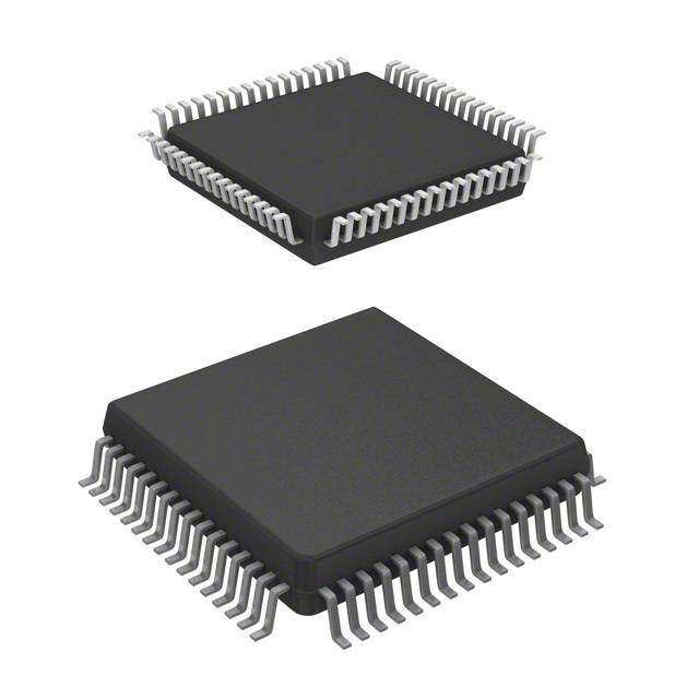
| 供应商器件封装 | 28-TSSOP |
| 其它名称 | 598-1122-5 |
| 包装 | 管件 |
| 安装类型 | 表面贴装 |
| 封装/外壳 | 28-TSSOP(0.173",4.40mm 宽) |
| 应用 | 车载音频 |
| 标准包装 | 50 |
| 类型 | 数字音频接口接收器 |


PDF Datasheet 数据手册内容提取
CS8415A 96 kHz Digital Audio Interface Receiver Features General Description ! Complete EIAJ CP1201, IEC-60958, AES3, The CS8415A is a monolithic CMOS device which re- S/PDIF-compatible Receiver ceives and decodes one of 7 channels of audio data ! +5.0 V Analog Supply (VA+) according to the IEC60958, S/PDIF, EIAJ CP1201, or AES3. The CS8415A has a serial digital audio output ! +3.3 V or +5.0 V Digital Interface (VL+) port and comprehensive control ability through a 4-wire ! 7:1 S/PDIF Input MUX microcontroller port. Channel status and user data are assembled in block-sized buffers, making read access ! Flexible 3-wire Serial Digital Output Port easy. ! 8-kHz to 96-kHz Sample Frequency Range A low-jitter clock recovery mechanism yields a very ! Low-jitter Clock Recovery clean recovered clock from the incoming AES3 stream. ! Pin and Microcontroller Read Access to Stand-alone operation allows systems with no micro- Channel Status and User Data controller to operate the CS8415A with dedicated output pins for channel status data. ! Microcontroller and Standalone Modes The CS8415A is available in a 28-pin TSSOP and SOIC ! Differential Cable Receiver package in both Commerical (-10 to +70°C) and Indus- ! On-chip Channel Status and User Data Buffer trial grades (-40 to +85° C). The CDB8415A Customer Memories Demonstration board is also available for device evalu- ation and implementation suggestions. Please refer to ! Auto-detection of Compressed Audio Input page2 for ordering information. Streams Target applications include A/V receivers, CD-R, DVD ! Decodes CD Q Sub-Code receivers, multimedia speakers, digital mixing consoles, ! OMCK System Clock Mode effects processors, set-top boxes, and computer and automotive audio systems. VA+ AGND FILT RERR RMCK VL+ DGND OMCK RXN0 Receiver OLRCK Clock& AES3 C&Ubit Serial Data S/PDIF Data Audio OSCLK RXP6 Recovery Decoder Buffer Output SDOUT RXP5 RXP4 7:1 RXP3 MUX Control Misc. Port& RXP2 Control Registers RXP1 RXP0 H/S RST EMPH U SDA/ SCL/ AD1/ AD0/ INT CDOUT CCLK CDIN CS Copyright © Cirrus Logic, Inc. 2005 AUGUST '05 http://www.cirrus.com (All Rights Reserved) DS470F4
CS8415A ORDERING INFORMATION Temp Product Description Package Grade Range Pb-Free Container Order Number Rail CS8415A-CZZ YES Tape and Reel CS8415A-CZZR Commercial -10 to +70°C 28- Rail CS8415A-CZ NO TSSOP Tape and Reel CS8415A-CZR 96 kHz Digital Rail CS8415A-IZZ CS8415A Audio Interface Industrial -40 to +85°C YES Tape and Reel CS8415A-IZZR Receiver Rail CS8415A-CSZ YES Tape and Reel CS8415A-CSZR 28-SOIC Commercial -10 to +70°C Rail CS8415A-CS NO Tape and Reel CS8415A-CSR CDB8415A CS8415AEvaluationBoard - - - - CDB8415A 2 DS470F4
CS8415A TABLE OF CONTENTS 1. CHARACTERISTICS AND SPECIFICATIONS .....................................................................................6 SPECIFIED OPERATING CONDITIONS..............................................................................................6 ABSOLUTE MAXIMUM RATINGS........................................................................................................6 DC ELECTRICAL CHARACTERISTICS...............................................................................................6 DIGITAL INPUT CHARACTERISTICS..................................................................................................7 DIGITAL INTERFACE SPECIFICATIONS............................................................................................7 SWITCHING CHARACTERISTICS.......................................................................................................7 SWITCHING CHARACTERISTICS - SERIAL AUDIO PORTS.............................................................8 SWITCHING CHARACTERISTICS - CONTROL PORT - SPI MODE...................................................9 SWITCHING CHARACTERISTICS - CONTROL PORT - I²C MODE..................................................10 2. TYPICAL CONNECTION DIAGRAM ..................................................................................................11 3. GENERAL DESCRIPTION ..................................................................................................................12 3.1 AES3 and S/PDIF Standards Documents ....................................................................................12 4. SERIAL AUDIO OUTPUT PORT .........................................................................................................13 5. AES3 RECEIVER ................................................................................................................................15 5.1 7:1 S/PDIF Input Multiplexer .........................................................................................................15 5.2 OMCK System Clock Mode ..........................................................................................................15 5.3 PLL, Jitter Attenuation, and Varispeed .........................................................................................15 5.4 Error Reporting and Hold Function ...............................................................................................15 5.5 Channel Status Data Handling .....................................................................................................16 5.6 User Data Handling ......................................................................................................................16 5.7 Non-Audio Auto-Detection ............................................................................................................16 5.8 Mono Mode Operation ..................................................................................................................17 6. CONTROL PORT DESCRIPTION AND TIMING ................................................................................18 6.1 SPITM Mode .................................................................................................................................18 6.2 I²C Mode .......................................................................................................................................19 6.3 Interrupts ......................................................................................................................................19 7. CONTROL PORT REGISTER SUMMARY .........................................................................................20 7.1 Memory Address Pointer (MAP) ...................................................................................................20 8. CONTROL PORT REGISTER BIT DEFINITIONS ..............................................................................21 8.1 Control 1 (01h) ............................................................................................................................21 8.2 Control 2 (02h) ..............................................................................................................................21 8.3 Clock Source Control (04h) ..........................................................................................................22 8.4 Serial Audio Output Port Data Format (06h) .................................................................................22 8.5 Interrupt 1 Status (07h) (Read Only) ............................................................................................23 8.6 Interrupt 2 Status (08h) (Read Only) ............................................................................................24 8.7 Interrupt 1 Mask (09h) ..................................................................................................................24 8.8 Interrupt 1 Mode MSB (0Ah) and Interrupt 1 Mode LSB (0Bh) .....................................................24 8.9 Interrupt 2 Mask (0Ch) ..................................................................................................................24 8.10 Interrupt 2 Mode MSB (0Dh) and Interrupt 2 Mode LSB (0Eh) ...................................................25 8.11 Receiver Channel Status (0Fh) (Read Only) ..............................................................................25 8.12 Receiver Error (10h) (Read Only) ...............................................................................................26 8.13 Receiver Error Mask (11h) ..........................................................................................................26 8.14 Channel Status Data Buffer Control (12h) ..................................................................................27 8.15 User Data Buffer Control (13h) ...................................................................................................27 8.16 Q-Channel Subcode Bytes 0 to 9 (14h - 1Dh) (Read Only) ........................................................28 8.17 OMCK/RMCK Ratio (1Eh) (Read Only) ......................................................................................28 8.18 C-bit or U-bit Data Buffer (20h - 37h) ..........................................................................................28 8.19 CS8415A I.D. and Version Register (7Fh) (Read Only) .............................................................28 9. PIN DESCRIPTION - SOFTWARE MODE ..........................................................................................29 10. HARDWARE MODE ..........................................................................................................................31 10.1 Serial Audio Port Formats ..........................................................................................................31 11. PIN DESCRIPTION - HARDWARE MODE .......................................................................................32 12. APPLICATIONS ...............................................................................................................................34 12.1 Reset, Power Down and Start-Up ..............................................................................................34 12.2 ID Code and Revision Code .......................................................................................................34 12.3 Power Supply, Grounding, and PCB Layout ..............................................................................34 DS470F4 3
CS8415A 13. APPENDIX A: EXTERNAL AES3/SPDIF/IEC60958 RECEIVER COMPONENTS ..........................35 13.1 AES3 Receiver External Components ........................................................................................35 13.2 Isolating Transformer Requirements ..........................................................................................36 14. APPENDIX B: CHANNEL STATUS AND USER DATA BUFFER MANAGEMENT ........................37 14.1 AES3 Channel Status (C) Bit Management ................................................................................37 14.2 Accessing the E Buffer ...............................................................................................................37 14.2.1 Reserving the First 5 Bytes in the E Buffer ....................................................................38 14.2.2 Serial Copy Management System (SCMS) ....................................................................38 14.2.3 Channel Status Data E Buffer Access ...........................................................................38 14.2.3.1 One-Byte Mode..................................................................................................38 14.2.3.2 Two-Byte Mode..................................................................................................39 14.3 AES3 User (U) Bit Management .................................................................................................39 15. APPENDIX C: PLL FILTER ...............................................................................................................40 15.1 General .......................................................................................................................................40 15.2 External Filter Components ........................................................................................................41 15.2.1 General ..........................................................................................................................41 15.2.2 Capacitor Selection ........................................................................................................41 15.2.3 Circuit Board Layout ......................................................................................................41 15.3 Component Value Selection .......................................................................................................42 15.3.1 Identifying the Part Revision ..........................................................................................42 15.3.2 External Components ....................................................................................................42 15.3.3 Jitter Tolerance ..............................................................................................................43 15.3.4 Jitter Attenuation ............................................................................................................44 16. REVISION HISTORY ........................................................................................................................45 4 DS470F4
CS8415A LIST OF FIGURES Figure 1. Audio Port Master Mode Timing...................................................................................................8 Figure 2. Audio Port Slave Mode and Data Input Timing.............................................................................8 Figure 3. SPI Mode Timing..........................................................................................................................9 Figure 4. I²C Mode Timing.........................................................................................................................10 Figure 5. Recommended Connection Diagram for Software Mode...........................................................11 Figure 6. Serial Audio Output Example Formats........................................................................................14 Figure 7. AES3 ReceiverTiming for C & U Pin Output Data......................................................................17 Figure 8. Control Port Timing in SPI Mode................................................................................................18 Figure 9. Control Port Timing in I²C Mode.................................................................................................19 Figure 10. Hardware Mode........................................................................................................................31 Figure 11. Professional Input Circuit..........................................................................................................36 Figure 12. Transformerless Professional Input Circuit...............................................................................36 Figure 13. Consumer Input Circuit.............................................................................................................36 Figure 14. S/PDIF MUX Input Circuit.........................................................................................................36 Figure 15. TTL/CMOS Input Circuit............................................................................................................36 Figure 16. Channel Status Data Buffer Structure.......................................................................................37 Figure 17. Flowchart for Reading the E Buffer...........................................................................................38 Figure 18. PLL Block Diagram...................................................................................................................40 Figure 19. Recommended Layout Example...............................................................................................41 Figure 20. Jitter Tolerance Template.........................................................................................................43 Figure 21. Revision A.................................................................................................................................44 Figure 22. Revision A1...............................................................................................................................44 Figure 23. Revision A2 using A1 Values....................................................................................................44 Figure 24. Revision A2 using A2* Values..................................................................................................44 LIST OF TABLES Table 1. Control Register Map Summary...................................................................................................20 Table 2. Equivalent Software Mode Bit Definitions....................................................................................31 Table 3. Hardware Mode Start-Up Options................................................................................................31 Table 4. Second Line Part Marking............................................................................................................42 Table 5. Fs = 8 to 96kHz...........................................................................................................................42 Table 6. Fs = 32 to 96kHz.........................................................................................................................42 Table 7. Revision History...........................................................................................................................45 DS470F4 5
CS8415A 1. CHARACTERISTICS AND SPECIFICATIONS All Min/Max characteristics and specifications are guaranteed over the Specified Operating Conditions. Typical per- formance characteristics and specifications are derived from measurements taken at nominal supply voltages and T = 25°C. A SPECIFIED OPERATING CONDITIONS AGND, DGND = 0V, all voltages with respect to 0V. Parameter Symbol Min Typ Max Units Power Supply Voltage VA+ 4.5 5.0 5.5 V (Note 1) VL+ 2.85 3.3 or 5.0 5.5 V Ambient Operating Temperature: Commercial Grade TA -10 - +70 °C Industrial Grade -40 - +85 Notes: 1. I²C protocol is supported only in VL+ = 5.0V mode. ABSOLUTE MAXIMUM RATINGS AGND, DGND = 0V; all voltages with respect to 0V. Operation beyond these limits may result in permanent dam- age to the device. Normal operation is not guaranteed at these extremes. Parameter Symbol Min Max Units Power Supply Voltage VL+,VA+ - 6.0 V Input Current, Any Pin Except Supplies (Note 2) I - ±10 mA in Input Voltage V -0.3 (VL+) + 0.3 V in Ambient Operating Temperature (power applied) T -55 125 °C A Storage Temperature T -65 150 °C stg 2. Transient currents of up to 100mA will not cause SCR latch-up. DC ELECTRICAL CHARACTERISTICS AGND = DGND = 0V; all voltages with respect to 0V. Parameters Symbol Min Typ Max Units Power-down Mode (Note 3) Supply Current in power down VA+ - 20 - µA VL+ = 3.3V - 60 - µA VL+ = 5.0V - 60 - µA Normal Operation (Note 4) Supply Current at 48kHz frame rate VA+ - 6.3 - mA VL+ = 3.3V - 30.1 - mA VL+ = 5.0V - 46.5 - mA Supply Current at 96kHz frame rate VA+ - 6.6 - mA VL+ = 3.3V - 44.8 - mA VL+ = 5.0V - 76.6 - mA 3. Power Down Mode is defined as RST = LO with all clocks and data lines held static. 4. Normal operation is defined as RST = HI. 6 DS470F4
CS8415A DIGITAL INPUT CHARACTERISTICS Parameters Symbol Min Typ Max Units Input Leakage Current I - ±1 ±10 µA in Differential Input Voltage, RXP0 to RXN0 V - 200 - mV TH DIGITAL INTERFACE SPECIFICATIONS AGND = DGND = 0V; all voltages with respect to 0V. Parameters Symbol Min Max Units High-Level Output Voltage (I = -3.2mA) V (VL+) - 1.0 - V OH OH Low-Level Output Voltage (I = 3.2mA) V - 0.4 V OH OL High-Level Input Voltage, except RX V 2.0 (VL+) + 0.3 V n IH Low-Level Input Voltage, except RX (Note 5) V -0.3 0.4/0.8 V n IL 5. At 5.0V mode, V = 0.8V (Max), at 3.3V mode, V =0.4V (Max). IL IL SWITCHING CHARACTERISTICS Inputs: Logic 0 = 0V, Logic 1 = VL+; C = 20pF. L Parameter Symbol Min Typ Max Units RST pin Low Pulse Width 200 - - µs PLL Clock Recovery Sample Rate Range 8.0 - 108.0 kHz RMCK output jitter (Note 6) - 200 - ps RMS RMCK output duty cycle 40 50 60 % 6. Cycle-to-cycle using 32to96kHz external PLL filter components. DS470F4 7
CS8415A SWITCHING CHARACTERISTICS - SERIAL AUDIO PORTS Inputs: Logic 0 = 0V, Logic 1 = VL+; C = 20pF. L Parameter Symbol Min Typ Max Units OSCLK Active Edge to SDOUT Output Valid (Note 7) t - - 20 ns dpd Master Mode RMCK to OSCLK active edge delay (Note 7) t 0 - 10 ns smd RMCK to OLRCK delay (Note 8) t 0 - 10 ns lmd OSCLK and OLRCK Duty Cycle - 50 - % Slave Mode OSCLK Period (Note 9) t 36 - - ns sckw OSCLK Input Low Width t 14 - - ns sckl OSCLK Input High Width t 14 - - ns sckh OSCLK Active Edge to OLRCK Edge (Note 7, 8, 10) t 20 - - ns lrckd OLRCK Edge Setup Before OSCLK Active Edge t 20 - - ns lrcks Notes 7, 8, 11 7. The active edges of OSCLK are programmable. 8. The polarity OLRCK is programmable. 9. No more than 128 SCLK per frame. 10. This delay is to prevent the previous OSCLK edge from being interpreted as the first one after OLRCK has changed. 11. This setup time ensures that this OSCLK edge is interpreted as the first one after OLRCK has changed. OSCLK (output) OLRCK (input) tlrckd tlrcks tsckh tsckl OLRCK (output) t OSCLK smd t (input) lmd RMCK tsckw (output) tdpd Hardware Mode RMCK SDOUT (output) Software Mode Figure 1. Audio Port Master Mode Timing Figure 2. Audio Port Slave Mode and Data Input Timing 8 DS470F4
CS8415A SWITCHING CHARACTERISTICS - CONTROL PORT - SPI MODE Inputs: Logic 0 = 0V, Logic 1 = VL+; C = 20pF. L Parameter Symbol Min Typ Max Units CCLK Clock Frequency (Note 12) f 0 - 6.0 MHz sck CS High Time Between Transmissions t 1.0 - - µs csh CS Falling to CCLK Edge t 20 - - ns css CCLK Low Time t 66 - - ns scl CCLK High Time t 66 - - ns sch CDIN to CCLK Rising Setup Time t 40 - - ns dsu CCLK Rising to DATA Hold Time (Note 13) t 15 - - ns dh CCLK Falling to CDOUT Stable t - - 50 ns pd Rise Time of CDOUT t - - 25 ns r1 Fall Time of CDOUT t - - 25 ns f1 Rise Time of CCLK and CDIN (Note 14) t - - 100 ns r2 Fall Time of CCLK and CDIN (Note 14) t - - 100 ns f2 12. If Fs is lower than 46.875kHz, the maximum CCLK frequency should be less than 128Fs. This is dic- tated by the timing requirements necessary to access the Channel Status and User Bit buffer memory. Access to the control register file can be carried out at the full 6MHz rate. The minimum allowable input sample rate is 8kHz, so choosing CCLK to be less than or equal to 1.024MHz should be safe for all possible conditions. 13. Data must be held for sufficient time to bridge the transition time of CCLK. 14. For f <1MHz. sck CS t t tcss scl sch tcsh CCLK t t r2 f2 CDIN t dsu t dh t pd CDOUT Figure 3. SPI Mode Timing DS470F4 9
CS8415A SWITCHING CHARACTERISTICS - CONTROL PORT - I²C MODE (Note 15), Inputs: Logic 0 = 0V, Logic 1 = VL+; C = 20pF. L Parameter Symbol Min Typ Max Units SCL Clock Frequency fscl - - 100 kHz Bus Free Time Between Transmissions t 4.7 - - µs buf Start Condition Hold Time (prior to first clock pulse) t 4.0 - - µs hdst Clock Low Time t 4.7 - - µs low Clock High Time t 4.0 - - µs high Setup Time for Repeated Start Condition t 4.7 - - µs sust SDA Hold Time from SCL Falling (Note 16) t 0 - - µs hdd SDA Setup Time to SCL Rising t 250 - - ns sud Rise Time of Both SDA and SCL Lines t - - 25 ns r Fall Time of Both SDA and SCL Lines t - - 25 ns f Setup Time for Stop Condition t 4.7 - - µs susp 15. I²C protocol is supported only in VL+ = 5.0V mode. 16. Data must be held for sufficient time to bridge the 25ns transition time of SCL. Repeated Stop Start Start Stop SDA tbuf thdst thigh thdst tf tsusp SCL tlow thdd tsud tsust tr Figure 4. I²C Mode Timing 10 DS470F4
CS8415A 2. TYPICAL CONNECTION DIAGRAM Ferrite* +5.0 V Bead +3.3 V or +5.0 V Analog 0.1µF Digital Supply Supply* 0.1µF VA+ VL+ CS8415A RXP6 RXP5 OLRCK 3-wireSerial ** RXP4 OSCLK AudioInput AES3/ SPDIF RXP3 SDOUT Device RXP2 Sources RXP1 RXP0 RXN0 SDA/CDOUT AD0/CS ClockControl RMCK SCL/CCLK Microcontroller AD1/CDIN INT U EMPH/AD2 DGND2 Hardware RERR Control RST H/S AGND FILT DGND RFILT CFILT CRIP *AseparateanalogsupplyisonlynecessaryinapplicationswhereRMCKisused forajittersensitivetask.ForapplicationswhereRMCKisnotusedforajitter sensitivetask,connectVA+toVD+viaaferritebead.Keepthedecoupling capacitorbetweenVA+andAGND. ** Please see section 5.1 "7:1 S/PDIF Input Multiplexer" and Appendix A for typical input configurations and recommended input circuits. Figure 5. Recommended Connection Diagram for Software Mode DS470F4 11
CS8415A 3. GENERAL DESCRIPTION The CS8415A is a monolithic CMOS device which receives and decodes audio data according to the AES3, IEC60958, S/PDIF, and EIAJ CP1201 interface standards. Input data is either differential or single-ended. A low-jitter clock is recovered from the incoming data using a PLL. The decoded audio data is output through a configurable, 3-wire output port. The channel status and user data are assembled in block-sized buffers and may be accessed through an SPI or I²C microcontroller port. For systems with no microcontroller, a stand-alone mode allows direct access to channel status and user data output pins. Target applications include AVR, CD-R, DAT, DVD, multimedia speakers, MD and VTR equipment, mixing con- soles, digital audio transmission and receiving equipment, high-quality D/A and A/D converters, effects processors, set-top boxes, and computer audio systems. Figure5 shows the supply and external connections to the CS8415A, when configured for operation with a micro- controller. 3.1 AES3 and S/PDIF Standards Documents This data sheet assumes that the user is familiar with the AES3 and S/PDIF data formats. It is advisable to have current copies of the AES3 and IEC60958 specifications on hand for easy reference. The latest AES3 standard is available from the Audio Engineering Society or ANSI at www.aes.org or www.ansi.org. Obtain the latest IEC60958 standard from ANSI or from the International Electrotechnical Commission at www.iec.ch. The latest EIAJ CP-1201 standard is available from the Japanese Electronics Bureau. Cirrus Logic Application Note 22: Overview of Digital Audio Interface Data Structures contains a useful tu- torial on digital audio specifications, but it should not be considered a substitute for the standards. The paper An Understanding and Implementation of the SCMS Serial Copy Management System for Digital Audio Transmission, by Clifton Sanchez, is an excellent tutorial on SCMS. It is available from the AES as preprint 3518. 12 DS470F4
CS8415A 4. SERIAL AUDIO OUTPUT PORT A 3-wire serial audio output port is provided. The port can be adjusted to suit the attached device setting the control registers. The following parameters are adjustable: master or slave, serial clock frequency, audio data resolution, left or right justification of the data relative to left/right clock, optional one-bit cell delay of the first data bit, the polar- ity of the bit clock, and the polarity of the left/right clock. By setting the appropriate control bits, many formats are possible. Figure6 shows the selection of common output formats including the control bit settings. It should be noted that in right-justified mode, the serial audio output data is "MSB extended". This means that in a sub-frame where the MSB of the data is '1', all bits preceding the MSB in the sub-frame will also be '1'. Conversely, in a sub-frame where the MSB of the data is '0', all bits preceding the MSB in the sub-frame will also be '0'. A special AES3 direct output format is included, which allows the serial output port access to the V, U, and C bits embedded in the serial audio data stream. The P bit is replaced by a Z bit that marks the subframe just prior to the start of each block. The received channel status block start signal is only available in hardware mode, as the RCBL pin. In master mode, the left/right clock and the serial bit clock are outputs, derived from the recovered RMCK clock. In slave mode, the left/right clock and the serial bit clock are inputs. The left/right clock must be synchronous to the appropriate master clock, but the serial bit clock can be asynchronous and discontinuous if required. By appropri- ate phasing of the left/right clock and control of the serial clocks, multiple CS8415As can share one serial port. The left/right clock should be continuous, but the duty cycle can be less than the specified typical value of 50% if enough serial clocks are present in each phase to clock all the data bits. When in slave mode, the serial audio out- put port must not be set for right-justified data. When using the serial audio output port in slave mode with an OLRCK input which is asynchronous to the incoming AES3 data, an interrupt bit (OSLIP) is provided to indicate DS470F4 13
CS8415A when repeated or dropped samples occur. The CS8415A allows immediate mute of the serial audio output port audio data by the MUTESAO bit of Control Register 1. OLRCK Channel A Channel B Left Justified OSCLK (Out) SDOUT MSB LSB MSB LSB MSB OLRCK Channel A Channel B I²S OSCLK (Out) SDOUT MSB LSB MSB LSB MSB OLRCK Channel A Channel B Right Justified OSCLK (Out) SDOUT MSB Extended MSB LSB MSB Extended MSB LSB OLRCK Channel A Channel B Channel A Channel B AES3 Direct OSCLK (Out) SDOUT LSB MSB VUC LSB MSB VUCZ LSB MSB VUCZ LSB MSB VUC Frame 191 Frame 0 SOMS* SOSF* SORES[1:0]* SOJUST* SODEL* SOSPOL* SOLRPOL* Left Justified X X XX 0 0 0 0 I²S X X XX 0 1 0 1 Right Justified 1 X XX 1 0 0 0 AES3 Direct X X 11 0 0 0 0 X = don’t care to match format, but does need to be set to the desired setting * See Serial Output Data Format Register Bit Descriptions for an explanation of the meaning of each bit Figure 6. Serial Audio Output Example Formats 14 DS470F4
CS8415A 5. AES3 RECEIVER The CS8415A includes an AES3 digital audio receiver. A comprehensive buffering scheme provides read access to the channel status and user data. This buffering scheme is described in Appendix B. The AES3 receiver accepts and decodes audio and digital data according to the AES3, IEC60958 (S/PDIF), and EIAJ CP-1201 interface standards. The receiver consists of a differential input stage, driven through pins RXP0 and RXN0, a PLL-based clock recovery circuit, and a decoder which separates the audio data from the channel status and user data. External components are used to terminate and isolate the incoming data cables from the CS8415A. These com- ponents are detailed in Appendix A. 5.1 7:1 S/PDIF Input Multiplexer The CS8415A employs a 7:1 S/PDIF Input Multiplexer to accommodate up to seven channels of input digital audio data. Digital audio data is single-ended and input through the RXP[0:6] pins. When any portion of the multiplexer is implemented, unused RXP pins should be tied to ground, and RXN0 must be AC-coupled to ground. The multiplexer select line control is accessed through bits MUX[2:0] in the Control 2 register. The multiplexer defaults to RXP0. Therefore, the default configuration is for a differential signal to be input through RXP0 & RXN0. Please see Appendix A for recommended input circuits. 5.2 OMCK System Clock Mode A special clock switching mode is available that allows the clock that is input through the OMCK pin to be output through the RMCK pin. This feature is controlled by the SWCLK bit in register 1 of the control regis- ters. When the PLL loses lock, the frequency of the VCO drops to 300kHz. The clock switching mode allows the clock input through OMCK to be used as a clock in the system without any disruption when the PLL loses lock. For example, when the input is removed from the receiver. When SWCLK is enabled and this mode is implemented, RMCK is an output and is not bi-directional. This clock switching is performed glitch-free. Please note that internal circuitry associated with RMCK is not driven by OMCK. This means that OSCLK and OLRCK continue to be derived from the PLL and are not usable in this mode. This function is available only in software mode. 5.3 PLL, Jitter Attenuation, and Varispeed Please see Appendix C for general description of the PLL, selection of recommended PLL filter compo- nents, and layout considerations. Figure5 shows the recommended configuration of the two capacitors and one resistor that comprise the PLL filter. 5.4 Error Reporting and Hold Function While decoding the incoming AES3 data stream, the CS8415A can identify several kinds of error, indicated in the Receiver Error register. The UNLOCK bit indicates whether the PLL is locked to the incoming AES3 data. The V bit reflects the current validity bit status. The CONF (confidence) bit is the logical OR of BIP and UNLOCK. The BIP (bi-phase) error bit indicates an error in incoming bi-phase coding. The PAR (parity) bit indicates a received parity error. The error bits are "sticky" - they are set on the first occurrence of the associated error and will remain set until the user reads the register through the control port. This enables the register to log all unmasked errors that occurred since the last time the register was read. The Receiver Error Mask register allows masking of individual errors. The bits in this register serve as masks for the corresponding bits of the Receiver Error Register. If a mask bit is set to 1, the error is un- masked, which implies the following: its occurrence will be reported in the receiver error register, induce a DS470F4 15
CS8415A pulse on RERR, invoke the occurrence of a RERR interrupt, and affect the current audio sample according to the status of the HOLD bits. The HOLD bits allow a choice of holding the previous sample, replacing the current sample with zero (mute), or not changing the current audio sample. If a mask bit is set to 0, the error is masked, which implies the following: its occurrence will not be reported in the receiver error register, will not induce a pulse on RERR or generate a RERR interrupt, and will not affect the current audio sample. The QCRC and CCRC errors do not affect the current audio sample, even if unmasked. 5.5 Channel Status Data Handling The first 2 bytes of the Channel Status block are decoded into the Receiver Channel Status register. The setting of the CHS bit in the Channel Status Data Buffer Control register determines whether the channel status decodes are from the A channel (CHS = 0) or B channel (CHS = 1). The PRO (professional) bit is extracted directly. For consumer data, the COPY (copyright) bit is extracted, and the category code and L bits are decoded to determine SCMS status, indicated by the ORIG (original) bit. If the category code is set to General on the incoming AES3 stream, copyright will always be indicated even when the stream indicates no copyright. Finally, the AUDIO bit is extracted and used to set an AUDIO indicator, as described in the Non-audio Auto-detection section below. If 50/15µs pre-emphasis is detected, the state of the EMPH pin is adjusted accordingly. The encoded channel status bits which indicate sample word length are decoded according to AES3-1992 or IEC 60958. Audio data routed to the serial audio output port is unaffected by the word length settings and all 24 bits are passed on as received. Appendix A describes the overall handling of Channel Status and User data. 5.6 User Data Handling The incoming user data is buffered in a user accessible buffer. Received user data may also be output to the U pin under the control of a control register bit. Depending on the clocking options selected, there may not be a clock available to qualify the U data output. Figure7 illustrates the timing. If the incoming user data bits have been encoded as Q-channel subcode, the data is decoded and presented in 10 consecutive reg- ister locations. An interrupt may be enabled to indicate the decoding of a new Q-channel block, which may be read through the control port. 5.7 Non-Audio Auto-Detection An AES3 data stream may be used to convey non-audio data, thus it is important to know whether the in- coming AES3 data stream is digital audio or not. This information is typically conveyed in channel status bit 1 (AUDIO), which is extracted automatically by the CS8415A. However, certain non-audio sources, such as AC-3® or MPEG encoders, may not adhere to this convention, and the bit may not be properly set. The CS8415A AES3 receiver can detect such non-audio data. This is accomplished by looking for a 96-bit sync code, consisting of 0x0000, 0x0000, 0x0000, 0x0000, 0xF872, and 0x4E1F. When the sync code is detect- ed, an internal AUTODETECT signal will be asserted. If no additional sync codes are detected within the next 4096 frames, AUTODETECT will be de-asserted until another sync code is detected. The AUDIO bit in the Receiver Channel Status register is the logical OR of AUTODETECT and the received channel status bit 1. If non-audio data is detected, the data is still processed exactly as if it were normal audio. It is up to the user to mute the outputs as required. 16 DS470F4
CS8415A 5.8 Mono Mode Operation An AES3 stream may be used in more than one way to transmit 96kHz sample rate data. One method is to double the frame rate of the current format. This results in a stereo signal with a sample rate of 96kHz, carried over a single twisted pair cable. An alternate method is implemented using the 2 sub-frames in a 48- kHz frame rate AES3 signal to carry consecutive samples of a mono signal, resulting in a 96-kHz sample rate stream. This allows older equipment, whose AES3 transmitters and receivers are not rated for 96-kHz frame rate operation, to handle 96-kHz sample rate information. In this “mono mode”, 2 AES3 cables are needed for stereo data transfer. The CS8415A offers mono mode operation, controlled through the MMR control register bit. The receiver mono mode effectively doubles Fs compared to the input frame rate. The clock output on the RMCK pin tracks Fs, and so is doubled in frequency compared to stereo mode. The receiver will run at a frame rate of Fs/2, and the serial audio output port will run at Fs. Sub-frame A data will be routed to both the left and right data fields on SDOUT. Similarly, sub-frame B data will be routed to both the left and right data fields of the next word clock cycle of SDOUT. Using mono mode is only necessary if the serial audio output port must run at 96kHz. If the CS8415A is kept in normal stereo mode, and receives AES3 data arranged in mono mode, then the serial audio output port will run at 48kHz, with left and right data fields representing consecutive audio samples. RCBL Out VLRCK C, U Output - RCBL and C output are only available in hardware mode. - RCBL goes high 2 frames after receipt of a Z preamble, and is high for 16 frames. - VLRCK is a virtual word clock, which may not exist, but is used to illustrate the C/U timing. - VLRCK duty cycle is 50%. VLRCK frequency is always equal to the incoming frame rate. - If the serial audio output port is in master mode, VLRCK = OLRCK - If the serial audio output port is in slave mode, then VLRCK needs to be externally created, if required. - C and U transitions are aligned within ± 1% of VLRCK period to VLRCK edges. Figure 7. AES3 ReceiverTiming for C & U Pin Output Data DS470F4 17
CS8415A 6. CONTROL PORT DESCRIPTION AND TIMING The control port is used to access the registers, allowing the CS8415A to be configured for the desired operational modes and formats. In addition, Channel Status and User data may be read through the control port. The operation of the control port may be completely asynchronous with respect to the audio sample rates. However, to avoid potential interference problems, the control port pins should remain static if no operation is required. The control port has 2 modes: SPI and I²C, with the CS8415A acting as a slave device. SPI mode is selected if there is a high-to-low transition on the AD0/CS pin, after the RST pin has been brought high. I²C mode is selected by connecting the AD0/CS pin to VL+ or DGND, thereby permanently selecting the desired AD0 bit address state. 6.1 SPITM Mode In SPI mode, CS is the CS8415A chip select signal, CCLK is the control port bit clock (input into the CS8415A from the microcontroller), CDIN is the input data line from the microcontroller, CDOUT is the out- put data line to the microcontroller. Data is clocked in on the rising edge of CCLK and out on the falling edge. Figure8 shows the operation of the control port in SPI mode. To write to a register, bring CS low. The first seven bits on CDIN form the chip address and must be 0010000b. The eighth bit is a read/write indicator (R/W), which should be low to write. The next eight bits form the Memory Address Pointer (MAP), which is set to the address of the register that is to be updated. The next eight bits are the data which will be placed into the register designated by the MAP. During writes, the CDOUT output stays in the Hi-Z state. It may be externally pulled high or low with a 47kΩ resistor, if desired. There is a MAP auto increment capability, enabled by the INCR bit in the MAP register. If INCR is a zero, the MAP will stay constant for successive read or writes. If INCR is set to a 1, the MAP will autoincrement after each byte is read or written, allowing block reads or writes of successive registers. To read a register, the MAP has to be set to the correct address by executing a partial write cycle which finishes (CS high) immediately after the MAP byte. The MAP auto increment bit (INCR) may be set or not, as desired. To begin a read, bring CS low, send out the chip address and set the read/write bit (R/W) high. The next falling edge of CCLK will clock out the MSB of the addressed register (CDOUT will leave the high impedance state). If the MAP auto increment bit is set to 1, the data for successive registers will appear consecutively. CS CCLK CHIP CHIP ADDRESS MAP DATA ADDRESS CDIN 0010000 R/W MSB LSB 0010000 R/W byte 1 byte n HighImpedance CDOUT MSB LSB MSB LSB MAP=MemoryAddressPointer,8bits,MSBfirst Figure 8. Control Port Timing in SPI Mode 18 DS470F4
CS8415A 6.2 I²C Mode In I²C mode, SDA is a bidirectional data line. Data is clocked into and out of the part by the clock, SCL, with the clock to data relationship as shown in Figure9. There is no CS pin. Each individual CS8415A is given a unique address. Pins AD0 and AD1 form the two least significant bits of the chip address and should be connected to VL+ or DGND as desired. The EMPH pin is used to set the AD2 bit by connecting a resistor from the EMPH pin to VL+ or to DGND. The state of the pin is sensed while the CS8415A is being reset. The upper 4 bits of the 7-bit address field are fixed at 0010b. To communicate with a CS8415A, the chip address field, which is the first byte sent to the CS8415A, should match 0010b followed by the settings of the EMPH, AD1, and AD0. The eighth bit of the address is the R/W bit. If the operation is a write, the next byte is the Memory Address Pointer (MAP) which selects the register to be read or written. If the operation is a read, the contents of the register pointed to by the MAP will be output. Setting the auto increment bit in MAP allows successive reads or writes of consecutive registers. Each byte is separated by an acknowledge bit. The ACK bit is output from the CS8415A after each input byte is read, and is input to the CS8415A from the microcontroller after each transmitted byte. I²C mode is supported only with VL+ in 5V mode. 6.3 Interrupts The CS8415A has a comprehensive interrupt capability. The INT output pin is intended to drive the interrupt input pin on the host microcontroller. The INT pin may be set to be active-low, active-high or active-low with no active pull-up transistor. This last mode is used for active-low, wired-OR hook-ups, with multiple periph- erals connected to the microcontroller interrupt input pin. Many conditions can cause an interrupt, as listed in the interrupt status register descriptions. Each source may be masked off through mask register bits. In addition, each source may be set to rising edge, falling edge, or level-sensitive. Combined with the option of level-sensitive or edge-sensitive modes within the mi- crocontroller, many different configurations are possible, depending on the needs of the equipment design- er. Note1 Note2 Note3 SDA 0010 AD2-0 R/W ACK DATA7-0 ACK DATA7-0 ACK SCL Start Stop Figure 9. Control Port Timing in I²C Mode Notes: 1. AD2 is derived from a resistor attached to the EMPH pin. AD1 and AD0 are determined by the state of the corresponding pins. 2. If operation is a write, this byte contains the Memory Address Pointer, MAP. 3. If operation is a read, the last bit of the read should be NACK (high). DS470F4 19
CS8415A 7. CONTROL PORT REGISTER SUMMARY Addr Function 7 6 5 4 3 2 1 0 (HEX) 01 Control 1 SWCLK 0 MUTESAO 0 0 INT1 INT0 0 02 Control 2 0 HOLD1 HOLD0 RMCKF MMR MUX2 MUX1 MUX0 04 Clock Source Control 0 RUN 0 0 0 0 0 0 06 Serial Output Format SOMS SOSF SORES1 SORES0 SOJUST SODEL SOSPOL SOLRPOL 07 Interrupt 1 Status 0 OSLIP 0 0 0 DETC 0 RERR 08 Interrupt 2 Status 0 0 0 0 DETU 0 QCH 0 09 Interrupt 1 Mask 0 OSLIPM 0 0 0 DETCM 0 RERRM 0A Interrupt 1 Mode (MSB) 0 OSLIP1 0 0 0 DETC1 0 RERR1 0B Interrupt 1 Mode (LSB) 0 OSLIP0 0 0 0 DETC0 0 RERR0 0C Interrupt 2 Mask 0 0 0 0 DETUM 0 QCHM 0 0D Interrupt 2 Mode (MSB) 0 0 0 0 DETU1 0 QCH1 0 0E Interrupt 2 Mode (LSB) 0 0 0 0 DETU0 0 QCH0 0 0F Receiver CS Data AUX3 AUX2 AUX1 AUX0 PRO AUDIO COPY ORIG 10 Receiver Errors 0 QCRC CCRC UNLOCK V CONF BIP PAR 11 Receiver Error Mask 0 QCRCM CCRCM UNLOCKM VM CONFM BIPM PARM 12 CS Data Buffer Control 0 0 BSEL CBMR DETCI 0 CAM CHS 13 U Data Buffer Control 0 0 0 0 0 0 DETUI 0 14-1D Q sub-code Data 1E OMCK/RMCK Ratio ORR7 ORR6 ORR5 ORR4 ORR3 ORR2 ORR1 ORR0 20-37 C or U Data Buffer 7F ID and Version ID3 ID2 ID1 ID0 VER3 VER2 VER1 VER0 Table 1. Control Register Map Summary 7.1 Memory Address Pointer (MAP) 7 6 5 4 3 2 1 0 INCR MAP6 MAP5 MAP4 MAP3 MAP2 MAP1 MAP0 INCR - Auto Increment Address Control Bit Default = ‘0’ 0 - Disabled 1 - Enabled MAP6:MAP0 - Register address Note: Reserved registers must not be written to during normal operation. Some reserved registers are used for test modes, which can completely alter the normal operation of the CS8415A. 20 DS470F4
CS8415A 8. CONTROL PORT REGISTER BIT DEFINITIONS 8.1 Control 1 (01h) 7 6 5 4 3 2 1 0 SWCLK 0 MUTESAO 0 0 INT1 INT0 0 SWCLK - Controls output of OMCK on RMCK when PLL loses lock Default = ‘0’ 0 - RMCK default function 1 - OMCK output on RMCK pin MUTESAO - Mute control for the serial audio output port Default = ‘0’ 0 - Disabled 1 - Enabled INT1:0 - Interrupt output pin (INT) control Default = ‘00’ 00 - Active high; high output indicates interrupt condition has occurred 01 - Active low, low output indicates an interrupt condition has occurred 10 - Open drain, active low. Requires an external pull-up resistor on the INT pin. 11 - Reserved 8.2 Control 2 (02h) 7 6 5 4 3 2 1 0 0 HOLD1 HOLD0 RMCKF MMR MUX2 MUX1 MUX0 HOLD1:0 - Determine how received audio sample is affected when a receiver error occurs Default = ‘00’ 00 - Hold the last valid audio sample 01 - Replace the current audio sample with 00 (mute) 10 - Do not change the received audio sample 11 - Reserved RMCKF - Select recovered master clock output pin frequency. Default = ‘0’ 0 - RMCK is equal to 256 * Fs 1 - RMCK is equal to 128 * Fs MMR - Select AES3 receiver mono or stereo operation Default = ‘0’ 0 - Normal stereo operation 1 - A and B subframes treated as consecutive samples of one channel of data. Data is duplicated to both left and right parallel outputs of the AES receiver block. The sample rate (Fs) is doubled compared to MMR=0 DS470F4 21
CS8415A MUX2:0 - 7:1 S/PDIF Input Multiplexer Select Line Control Default = ‘000’ 000 - RXP0 001 - RXP1 010 - RXP2 011 - RXP3 100 - RXP4 101 - RXP5 110 - RXP6 111 - Reserved 8.3 Clock Source Control (04h) 7 6 5 4 3 2 1 0 0 RUN 0 0 0 0 0 0 This register configures the clock sources of various blocks. In conjunction with the Data Flow Control reg- ister, various Receiver/Transmitter/Transceiver modes may be selected. RUN - Controls the internal clocks, allowing the CS8415A to be placed in a “powered down”, low current consumption, state. Default = ‘0’ 0 - Internal clocks are stopped. Internal state machines are reset. The fully static control port is operational, allowing registers to be read or changed. Reading and writing the U and C data buffers is not possible. Pow- er consumption is low. 1 - Normal part operation. This bit must be written to the 1 state to allow the CS8415A to begin operation. All input clocks should be stable in frequency and phase when RUN is set to 1. 8.4 Serial Audio Output Port Data Format (06h) 7 6 5 4 3 2 1 0 SOMS SOSF SORES1 SORES0 SOJUST SODEL SOSPOL SOLRPOL SOMS - Master/Slave Mode Selector Default = ‘0’ 0 - Serial audio output port is in slave mode 1 - Serial audio output port is in master mode SOSF - OSCLK frequency (for master mode) Default = ‘0’ 0 - 64*Fs 1 - 128*Fs SORES1:0 - Resolution of the output data on SDOUT Default = ‘00’ 00 - 24-bit resolution 01 - 20-bit resolution 10 - 16-bit resolution 11 - Direct copy of the received NRZ data from the AES3 receiver (including C, U, and V bits, the time slot 22 DS470F4
CS8415A normally occupied by the P bit is used to indicate the location of the block start, SDOUT pin only, serial audio output port clock must be derived from the AES3 receiver recovered clock) SOJUST - Justification of SDOUT data relative to OLRCK Default = ‘0’ 0 - Left-justified 1 - Right-justified (master mode only) SODEL - Delay of SDOUT data relative to OLRCK, for left-justified data formats Default = ‘0’ 0 - MSB of SDOUT data occurs in the first OSCLK period after the OLRCK edge 1 - MSB of SDOUT data occurs in the second OSCLK period after the OLRCK edge SOSPOL - OSCLK clock polarity Default = ‘0’ 0 - SDOUT sampled on rising edges of OSCLK 1 - SDOUT sampled on falling edges of OSCLK SOLRPOL - OLRCK clock polarity Default = ‘0’ 0 - SDOUT data is for the left channel when OLRCK is high 1 - SDOUT data is for the right channel when OLRCK is high 8.5 Interrupt 1 Status (07h) (Read Only) 7 6 5 4 3 2 1 0 0 OSLIP 0 0 0 DETC 0 RERR For all bits in this register, a “1” means the associated interrupt condition has occurred at least once since the register was last read. A ”0” means the associated interrupt condition has NOT occurred since the last reading of the register. Reading the register resets all bits to 0, unless the interrupt mode is set to level and the interrupt source is still true. Status bits that are masked off in the associated mask register will always be “0” in this register. This register defaults to 00h. OSLIP - Serial audio output port data slip interrupt When the serial audio output port is in slave mode, and OLRCK is asynchronous to the port data source, This bit will go high every time a data sample is dropped or repeated. DETC - D to E C-buffer transfer interrupt. Indicates the completion of a D to E C-buffer transfer. See “Channel Status and User Data Buffer Manage- ment” on page 38 for more information. RERR - A receiver error has occurred. The Receiver Error register may be read to determine the nature of the error which caused the interrupt. DS470F4 23
CS8415A 8.6 Interrupt 2 Status (08h) (Read Only) 7 6 5 4 3 2 1 0 0 0 0 0 DETU 0 QCH 0 For all bits in this register, a “1” means the associated interrupt condition has occurred at least once since the register was last read. A ”0” means the associated interrupt condition has NOT occurred since the last reading of the register. Reading the register resets all bits to 0, unless the interrupt mode is set to level and the interrupt source is still true. Status bits that are masked off in the associated mask register will always be “0” in this register. This register defaults to 00h. DETU - D to E U-buffer transfer interrupt. Indicates the completion of a D to E U-buffer transfer. See “Channel Status and User Data Buffer Manage- ment” on page 38 for more information. QCH - A new block of Q-subcode data is available for reading. The data must be completely read within 588 AES3 frames after the interrupt occurs to avoid corruption of the data by the next block. 8.7 Interrupt 1 Mask (09h) 7 6 5 4 3 2 1 0 0 OSLIPM 0 0 0 DETCM 0 RERRM The bits of this register serve as a mask for the Interrupt 1 register. If a mask bit is set to 1, the error is un- masked, meaning that its occurrence will affect the INT pin and the status register. If a mask bit is set to 0, the error is masked, meaning that its occurrence will not affect the INT pin or the status register. The bit positions align with the corresponding bits in Interrupt 1 register. This register defaults to 00h. 8.8 Interrupt 1 Mode MSB (0Ah) and Interrupt 1 Mode LSB (0Bh) 7 6 5 4 3 2 1 0 0 OSLIP1 0 0 0 DETC1 0 RERR1 0 OSLIP0 0 0 0 DETC0 0 RERR0 The two Interrupt Mode registers form a 2-bit code for each Interrupt Register 1 function. There are three ways to set the INT pin active in accordance with the interrupt condition. In the Rising edge active mode, the INT pin becomes active on the arrival of the interrupt condition. In the Falling edge active mode, the INT pin becomes active on the removal of the interrupt condition. In Level active mode, the INT interrupt pin be- comes active during the interrupt condition. Be aware that the active level (Actice High or Low) only depends on the INT[1:0] bits. These registers default to 00. 00 - Rising edge active 01 - Falling edge active 10 - Level active 11 - Reserved 8.9 Interrupt 2 Mask (0Ch) 7 6 5 4 3 2 1 0 0 0 0 0 DETUM 0 QCHM 0 The bits of this register serve as a mask for the Interrupt 2 register. If a mask bit is set to 1, the error is un- masked, meaning that its occurrence will affect the INT pin and the status register. If a mask bit is set to 0, the error is masked, meaning that its occurrence will not affect the INT pin or the status register. The bit positions align with the corresponding bits in Interrupt 2 register. This register defaults to 00h. 24 DS470F4
CS8415A 8.10 Interrupt 2 Mode MSB (0Dh) and Interrupt 2 Mode LSB (0Eh) 7 6 5 4 3 2 1 0 0 0 0 0 DETU1 0 QCH1 0 0 0 0 0 DETU0 0 QCH0 0 The two Interrupt Mode registers form a 2-bit code for each Interrupt Register 1 function. There are three ways to set the INT pin active in accordance with the interrupt condition. In the Rising edge active mode, the INT pin becomes active on the arrival of the interrupt condition. In the Falling edge active mode, the INT pin becomes active on the removal of the interrupt condition. In Level active mode, the INT interrupt pin be- comes active during the interrupt condition. Be aware that the active level (Actice High or Low) only depends on the INT[1:0] bits. These registers default to 00. 00 - Rising edge active 01 - Falling edge active 10 - Level active 11 - Reserved 8.11 Receiver Channel Status (0Fh) (Read Only) 7 6 5 4 3 2 1 0 AUX3 AUX2 AUX1 AUX0 PRO AUDIO COPY ORIG The bits in this register can be associated with either channel A or B of the received data. The desired chan- nel is selected with the CHS bit of the Channel Status Data Buffer Control Register. AUX3:0 - Incoming auxiliary data field width, as indicated by the incoming channel status bits, decoded ac- cording to IEC60958 and AES3. 0000 - Auxiliary data is not present 0001 - Auxiliary data is 1 bit long 0010 - Auxiliary data is 2 bits long 0011 - Auxiliary data is 3 bits long 0100 - Auxiliary data is 4 bits long 0101 - Auxiliary data is 5 bits long 0110 - Auxiliary data is 6 bits long 0111 - Auxiliary data is 7 bits long 1000 - Auxiliary data is 8 bits long 1001 - 1111 Reserved PRO - Channel status block format indicator 0 - Received channel status block is in consumer format 1 - Received channel status block is in professional format AUDIO - Audio indicator 0 - Received data is linearly coded PCM audio 1 - Received data is not linearly coded PCM audio COPY - SCMS copyright indicator 0 - Copyright asserted 1 - Copyright not asserted If the category code is set to General in the incoming AES3 stream, copyright will always be indicated by COPY, even when the stream indicates no copyright. DS470F4 25
CS8415A ORIG - SCMS generation indicator, decoded from the category code and the L bit. 0 - Received data is 1st generation or higher 1 - Received data is original Note: COPY and ORIG will both be set to 1 if the incoming data is flagged as professional, or if the re- ceiver is not in use. 8.12 Receiver Error (10h) (Read Only) 7 6 5 4 3 2 1 0 0 QCRC CCRC UNLOCK V CONF BIP PAR This register contains the AES3 receiver and PLL status bits. Unmasked bits will go high on occurrence of the error, and will stay high until the register is read. Reading the register resets all bits to 0, unless the error source is still true. Bits that are masked off in the receiver error mask register will always be 0 in this register. This register defaults to 00h. QCRC - Q-subcode data CRC error indicator. Updated on Q-subcode block boundaries 0 - No error 1 - Error CCRC - Channel Status Block Cyclic Redundancy Check bit. Updated on CS block boundaries, valid in Pro mode 0 - No error 1 - Error UNLOCK - PLL lock status bit. Updated on CS block boundaries. 0 - PLL locked 1 - PLL out of lock V - Received AES3 Validity bit status. Updated on sub-frame boundaries. 0 - Data is valid and is normally linear coded PCM audio 1 - Data is invalid, or may be valid compressed audio CONF - Confidence bit. Updated on sub-frame boundaries. 0 - No error 1 - Confidence error. This is the logical OR of BIP and UNLOCK. BIP - Bi-phase error bit. Updated on sub-frame boundaries. 0 - No error 1 - Bi-phase error. This indicates an error in the received bi-phase coding. PAR - Parity bit. Updated on sub-frame boundaries. 0 - No error 1 - Parity error 26 DS470F4
CS8415A 8.13 Receiver Error Mask (11h) 7 6 5 4 3 2 1 0 0 QCRCM CCRCM UNLOCKM VM CONFM BIPM PARM The bits in this register serve as masks for the corresponding bits of the Receiver Error Register. If a mask bit is set to 1, the error is unmasked, meaning that its occurrence will appear in the receiver error register, will affect the RERR pin, will affect the RERR interrupt, and will affect the current audio sample according to the status of the HOLD bit. If a mask bit is set to 0, the error is masked, meaning that its occurrence will not appear in the receiver error register, will not affect the RERR pin, will not affect the RERR interrupt, and will not affect the current audio sample. The CCRC and QCRC bits behave differently from the other bits: they do not affect the current audio sample even when unmasked. This register defaults to 00h. 8.14 Channel Status Data Buffer Control (12h) 7 6 5 4 3 2 1 0 0 0 BSEL CBMR DETCI 0 CAM CHS BSEL - Selects the data buffer register addresses to contain User data or Channel Status data Default = ‘0’ 0 - Data buffer address space contains Channel Status data 1 - Data buffer address space contains User data CBMR - Control for the first 5 bytes of channel status “E” buffer Default = ‘0’ 0 - Allow D to E buffer transfers to overwrite the first 5 bytes of channel status data 1 - Prevent D to E buffer transfers from overwriting first 5 bytes of channel status data DETCI - D to E C-data buffer transfer inhibit bit. Default = ‘0’ 0 - Allow C-data D to E buffer transfers 1 - Inhibit C-data D to E buffer transfers CAM - C-data buffer control port access mode bit Default = ‘0’ 0 - One byte mode 1 - Two byte mode CHS - Channel select bit Default = ‘0’ 0 - Channel A information is displayed at the EMPH pin and in the receiver channel status register. Channel A information is output during control port reads when CAM is set to 0 (One Byte Mode) 1 - Channel B information is displayed at the EMPH pin and in the receiver channel status register. Channel B information is output during control port reads when CAM is set to 0 (One Byte Mode) DS470F4 27
CS8415A 8.15 User Data Buffer Control (13h) 7 6 5 4 3 2 1 0 0 0 0 0 0 0 DETUI 0 DETUI - D to E U-data buffer transfer inhibit bit. Default = ‘0’ 0 - Allow U-data D to E buffer transfers 1 - Inhibit U-data D to E buffer transfers 8.16 Q-Channel Subcode Bytes 0 to 9 (14h - 1Dh) (Read Only) The following 10 registers contain the decoded Q-channel subcode data 7 6 5 4 3 2 1 0 CONTROL CONTROL CONTROL CONTROL ADDRESS ADDRESS ADDRESS ADDRESS TRACK TRACK TRACK TRACK TRACK TRACK TRACK TRACK INDEX INDEX INDEX INDEX INDEX INDEX INDEX INDEX MINUTE MINUTE MINUTE MINUTE MINUTE MINUTE MINUTE MINUTE SECOND SECOND SECOND SECOND SECOND SECOND SECOND SECOND FRAME FRAME FRAME FRAME FRAME FRAME FRAME FRAME ZERO ZERO ZERO ZERO ZERO ZERO ZERO ZERO ABS MINUTE ABS MINUTE ABS MINUTE ABS MINUTE ABS MINUTE ABS MINUTE ABS MINUTE ABS MINUTE ABS SECOND ABS SECOND ABS SECONDABS SECOND ABS SECOND ABS SECOND ABS SECOND ABS SECOND ABS FRAME ABS FRAME ABS FRAME ABS FRAME ABS FRAME ABS FRAME ABS FRAME ABS FRAME Each byte is LSB first with respect to the 80 Q-subcode bits Q[79:0]. Thus bit 7 of address 14h is Q[0] while bit 0 of address 0Eh is Q[7]. Similarly bit 0 of address 1Dh corresponds to Q[79]. 8.17 OMCK/RMCK Ratio (1Eh) (Read Only) 7 6 5 4 3 2 1 0 ORR7 ORR6 ORR5 ORR4 ORR3 ORR2 ORR1 ORR0 This register allows the calculation of the incoming sample rate by the host microcontroller from the equation ORR=Fso/Fsi. The Fso is determined by OMCK, whose frequency is assumed to be 256Fso. ORR is rep- resented as an unsigned 2-bit integer and a 6-bit fractional part. The value is meaningful only after the PLL has reached lock. For example, if the OMCK is 12.288MHz, Fso would be 48kHz (48kHz = 12.288MHz/256). Then if the input sample rate is also 48kHz, you would get 1.0 from the ORR regis- > ter.(The value from the ORR register is hexadecimal, so the actual value you will get is 40h). If F /F 3 SO SI 63/ , ORR will saturate at the value FFh. Also, there is no hysteresis on ORR. Therefore a small amount of 64 jitter on either clock can cause the LSB ORR[0] to oscillate. ORR7:6 - Integer part of the ratio (Integer value=Integer(SRR[7:6])) ORR5:0 - Fractional part of the ratio (Fraction value=Integer(SRR[5:0])/64) 8.18 C-bit or U-bit Data Buffer (20h - 37h) Either channel status data buffer E or user data buffer E is accessible through these register addresses. 28 DS470F4
CS8415A 8.19 CS8415A I.D. and Version Register (7Fh) (Read Only) 7 6 5 4 3 2 1 0 ID3 ID2 ID1 ID0 VER3 VER2 VER1 VER0 ID3:0 - ID code for the CS8415A. Permanently set to 0100 VER3:0 - CS8415A revision level. Revision A is coded as 0001 DS470F4 29
CS8415A 9. PIN DESCRIPTION - SOFTWARE MODE SDA/CDOUT 1 28 SCL/CCLK AD0/CS 2 27 AD1/CDIN EMPH 3*+ 26 RXP6 RXP0 4* 25 RXP5 RXN0 5* *24 H/S VA+ 6* *23 VL+ AGND 7* *22 DGND FILT 8* *21 OMCK RST 9* 20 U RMCK 10* 19 INT RERR 11* *18 SDOUT RXP1 12 *17 OLRCK RXP2 13 *16 OSCLK RXP3 14 15 RXP4 *Pins which remain the same function in allmodes. +Pins which requireapulluporpulldown resistor to selectthe desired startup option. Pin Name # Pin Description Serial Control Data I/O (I²C) / Data Out (SPI) (Input/Output) - In I²C mode, SDA is the control I/O data SDA/CDOUT 1 line. SDA is open drain and requires an external pull-up resistor to VL+. In SPI mode, CDOUT is the out- put data from the control port interface on the CS8415A Address Bit 0 (I²C) / Control Port Chip Select (SPI) (Input) - A falling edge on this pin puts the CS8415A into SPI control port mode. With no falling edge, the CS8415A defaults to I²C mode. In I²C AD0/CS 2 mode, AD0 is a chip address pin. In SPI mode, CS is used to enable the control port interface on the CS8415A Pre-Emphasis (Output) - EMPH is low when the incoming Channel Status data indicates 50/15ms pre-emphasis. EMPH is high when the Channel Status data indicates no pre-emphasis or indicates pre- EMPH 3 emphasis other than 50/15ms. This is also a start-up option pin, and requires a 47kΩ resistor to either VL+ or DGND, which determines the AD2 address bit for the control port in I²C mode AES3/SPDIF Receiver Port (Input) - Differential line receiver inputs carrying AES3 data. RXP0 may be RXP0 4 used as a single-ended input as part of 7:1 S/PDIF Input MUX. If RXP0 is used in MUX, RXN0 must be RXN0 5 ac coupled to ground. 12 RXP1 13 Additional AES3/SPDIF Receiver Port (Input) - Single-ended receiver inputs carrying AES3 or S/PDIF RXP2 RXP3 14 digital data. These inputs, along with RXP0, comprise the 7:1 S/PDIF Input Multiplexer and select line RXP4 RXP5 15 control is accessed using the MUX2:0 bits in the Control 2 register. Please note that any unused inputs RXP6 25 should be tied to ground. See Appendix A for recommended input circuits. 26 Positive Analog Power (Input) - Positive supply for the analog section. Nominally +5.0V. This supply VA+ 6 should be as quiet as possible since noise on this pin will directly affect the jitter performance of the recovered clock 30 DS470F4
CS8415A Pin Name # Pin Description Analog Ground (Input) - Ground for the analog circuitry in the chip. AGND and DGND should be con- AGND 7 nected to a common ground area under the chip. PLL Loop Filter (Output) - An RC network should be connected between this pin and ground. See FILT 8 “Appendix C: PLL Filter” on page41 for recommended schematic and component values. Reset (Input) - When RST is low, the CS8415A enters a low power mode and all internal states are reset. On initial power up, RST must be held low until the power supply is stable, and all input clocks are RST 9 stable in frequency and phase. This is particularly true in hardware mode with multiple CS8415A devices where synchronization between devices is important Input Section Recovered Master Clock (Output) - Input section recovered master clock output when RMCK 10 PLL is used. Frequency defaults to 256x the sample rate (Fs) and may be set to 128x. Receiver Error (Output) - When high, indicates a problem with the operation of the AES3 receiver. The status of this pin is updated once per sub-frame of incoming AES3 data. Conditions that can cause RERR to go high are: validity, parity error, bi-phase coding error, confidence, QCRC and CCRC errors, RERR 11 as well as loss of lock in the PLL. Each condition may be optionally masked from affecting the RERR pin using the Receiver Error Mask Register. The RERR pin tracks the status of the unmasked errors: the pin goes high as soon as an unmasked error occurs and goes low immediately when all unmasked errors go away. OSCLK 16 Serial Audio Output Bit Clock (Input/Output) - Serial bit clock for audio data on the SDOUT pin Serial Audio Output Left/Right Clock (Input/Output) - Word rate clock for the audio data on the OLRCK 17 SDOUT pin. Frequency will be the output sample rate (Fs) SDOUT 18 Serial Audio Output Data (Output) - Audio data serial output pin Interrupt (Output) - Indicates errors and key events during the operation of the CS8415A. All bits affect- ing INT may be unmasked through bits in the control registers. The condition(s) that initiated interrupt INT 19 are readable through a control register. The polarity of the INT output, as well as selection of a standard or open drain output, is set through a control register. Once set true, the INT pin goes false only after the interrupt status registers have been read and the interrupt status bits have returned to zero U 20 User Data (Output) - Outputs User data from the AES3 receiver, see Figure7 for timing information System Clock (Input) - When the OMCK System Clock Mode is enabled using the SWCLK bit in the OMCK 21 Control 1 register, the clock signal input on this pin is output through RMCK. OMCK serves as reference signal for OMCK/RMCK ratio expressed in register 1Eh Digital Ground (Input) - Ground for the digital circuitry in the chip. DGND and AGND should be con- DGND 22 nected to a common ground area under the chip. VL+ 23 Positive Digital Power (Input) - Positive supply for the digital section. Typically +3.3V or +5.0V. Hardware/Software Mode Control (Input) - Determines the method of controlling the operation of the CS8415A, and the method of accessing CS and U data. In software mode, device control and CS and U H/S 24 data access is primarily through the control port, using a microcontroller. Hardware mode provides an alternate mode of operation and access to the CS and U data through dedicated pins. This pin should be permanently tied to VL+ or DGND Address Bit 1 (I²C) / Serial Control Data in (SPI) (Input) - In I²C mode, AD1 is a chip address pin. In AD1/CDIN 27 SPI mode, CDIN is the input data line for the control port interface Control Port Clock (Input) - Serial control interface clock and is used to clock control data bits into and SCL/CCLK 28 out of the CS8415A. In I²C mode, SCL requires an external pull-up resistor to VL+ DS470F4 31
CS8415A 10.HARDWARE MODE The CS8415A has a hardware mode which allows using the device without a microcontroller. Hardware mode is selected by connecting the H/S pin to VL+. Various pins change function in hardware mode, described in the hard- ware mode pin definition section. Hardware mode data flow is shown in Figure10. Audio data is input through the AES3 receiver, and routed to the serial audio output port. The PRO, COPY, ORIG, EMPH, and AUDIO channel status bits are output on pins. The decoded C and U bits are also output, clocked at both edges of OLRCK (master mode only, see Figure7).The cur- rent audio sample is passed unmodified to the serial audio output port if the validity bit is high, or a parity, bi-phase, or PLL lock error occurs. 10.1 Serial Audio Port Formats In hardware mode, only a limited number of alternative serial audio port formats are available. Table2 de- fines the equivalent software mode bit settings for each format. Start-up options are shown in Table3, and allow choice of the serial audio output port as a master or slave, and the serial audio port format. SOSF SORES1/0 SOJUST SODEL SOSPOL SOLRPOL OF1 - Left Justified 0 00 0 0 0 0 OF2 - I²S 24-bit data 0 00 0 1 0 1 OF3 - Right Justified, master mode only 0 00 1 0 0 0 OF4 - Direct AES3 data 0 11 0 0 0 0 Table 2. Equivalent Software Mode Bit Definitions SDOUT ORIG EMPH Function LO - - Serial Output Port is Slave HI - - Serial Output Port is Master - LO LO Left Justified - LO HI I²S 24-bit data - HI LO Right Justified - HI HI Direct AES3 data Table 3. Hardware Mode Start-Up Options VL+ H/S RXP AES3Rx Serial OLRCK RXN &Decoder AOuudtpiout OSDSOCLUKT C&UbitDataBuffer C U RMCK RERR NVERRCHS COPY ORIG EMPH PRO AUDIO RCBL Powersupplypins(VD+,VA+,DGND,AGND)&theresetpin(RST)andthePLLfilterpin(FILT) areomittedfromthisdiagram.PleaserefertotheTypicalConnectionDiagramforhook-updetails. Figure 10. Hardware Mode 32 DS470F4
CS8415A 11.PIN DESCRIPTION - HARDWARE MODE Pin Name # Pin Description COPY Channel Status Bit (Output) - Reflects the state of the Copyright Channel Status bit in the incoming COPY 1 AES3 data stream. If the category code is set to General, copyright will be indicated whatever the state of the Copyright bit. VL2+ 2 VL+ 23 Positive Digital Power (Input) - Typically +3.3V or +5.0V. VL3+ 27 Pre-Emphasis (Output) - EMPH is low when the incoming Channel Status data indicates 50/15ms pre- emphasis. EMPH is high when the Channel Status data indicates no pre-emphasis or indicates pre-empha- EMPH 3 sis other than 50/15ms. This pin is also a start-up option which, along with ORIG, determines the serial port format. A 47kΩ resistor to either VL+ or DGND is required. RXP0 4 AES3/SPDIF Receiver Port (Input) - Differential line receiver inputs for the AES3 biphase encoded data. RXN0 5 See Appendix A for recommended circuits. Positive Analog Power (Input) - Nominally +5.0V. This supply should be as quiet as possible since noise VA+ 6 on this pin will directly affect the jitter performance of the recovered clock. Analog Ground (Input) - Ground for the analog circuitry in the chip. AGND and DGND should be connected AGND 7 to a common ground area under the chip. PLL Loop Filter (Output) - An RC network should be connected between this pin and ground. See “Appen- FILT 8 dix C: PLL Filter” on page41 for recommended schematic and component values. Reset (Input) - When RST is low, the CS8415A enters a low power mode and all internal states are reset. On initial power up, RST must be held low until the power supply is stable, and all input clocks are stable in RST 9 frequency and phase. This is particularly true in hardware mode with multiple CS8415A devices where syn- chronization between devices is important. DS470F4 33
CS8415A Pin Name # Pin Description Recovered Master Clock (Output) - Recovered master clock output when PLL is locked to the incoming RMCK 10 AES3 stream. Frequency is 256x the sample rate (Fs). Receiver Error (Output) - When high, indicates an error condition in the AES3 receiver. The status of this RERR 11 pin is updated once per sub-frame of incoming AES3 data. Conditions that can cause RERR to go high are: validity bit high, parity error, bi-phase coding error, and loss of lock by the PLL. Receiver Channel Status Block (Output) -Indicates the beginning of a received channel status block. RCBL goes high two frames after the reception of a Z preamble, remains high for 16 frames while COPY, RCBL 12 ORIG, AUDIO, EMPH and PRO are updated, and returns low for the remainder of the block. RCBL changes on rising edges of RMCK. PRO Channel Status Bit (Output) - Reflects the state of the Professional/Consumer Channel Status bit in PRO 13 the incoming AES3 data stream. Low indicates Consumer and high indicates Professional. Channel Select (Input) - Selects which sub-frame’s channel status data is output on the EMPH, COPY, CHS 14 ORIG, PRO and AUDIO pins. Channel A is selected when CHS is low, channel B is selected when CHS is high. No Validity Receiver Error Indicator (Output) - A high output indicates a problem with the operation of the NVERR 15 AES3 receiver. The status of this pin is updated once per frame of incoming AES3 data. Conditions that cause NVERR to go high are: parity error, and bi-phase coding error, and loss of lock by the PLL. OSCLK 16 Serial Audio Output Bit Clock (Input/Output) - Serial bit clock for audio data on the SDOUT pin. Serial Audio Output Left/Right Clock (Input/Output) - Word rate clock for the audio data on the SDOUT OLRCK 17 pin. Frequency will be the output sample rate (Fs). Serial Audio Output Data (Output) - Audio data serial output pin. This pin is also a start-up option which SDOUT 18 determines if the serial audio port is master or slave. A 47kΩ resistor to either VL+ or DGND is required. Audio Channel Status Bit (Output) - Reflects the state of the audio/non audio Channel Status AUDIO 19 bit in the incoming AES3 data stream. When this bit is low a valid audio stream is indicated. DGND3 20 Digital Ground (Input) - Ground for the digital circuitry in the chip. DGND and AGND should be connected DGND2 21 to a common ground area under the chip. DGND 22 Hardware/Software Mode Control (Input) - Determines the method of controlling the operation of the CS8415A, and the method of accessing CS and U data. In software mode, device control and CS and U H/S 24 data access is primarily through the control port, using a microcontroller. Hardware mode provides an alter- nate mode of operation and access to the CS and U data through dedicated pins. This pin should be perma- nently tied to VL+ or DGND. User Data (Output) - Outputs user data from the AES3 receiver, clocked by the rising and falling edges of U 25 OLRCK. Channel Status Data (Output) - Outputs channel status data from the AES3 receiver, clocked by the rising C 26 and falling edges of OLRCK. Original Channel Status (Output) - SCMS generation indicator. This is decoded from the incoming cate- gory code and the L bit in the Channel Status bits. A low output indicates that the source of the audio data ORIG 28 stream is a copy not an original. A high indicates that the audio data stream is original. This pin is also a start-up option which, along with EMPH, determines the serial audio port format. A 47kΩ resistor to either VL+ or DGND is required. 34 DS470F4
CS8415A 12. APPLICATIONS 12.1 Reset, Power Down and Start-Up When RST is low, the CS8415A enters a low-power mode and all internal states are reset, including the control port and registers, and the outputs are muted. When RST is high, the control port becomes opera- tional and the desired settings should be loaded into the control registers. Writing a 1 to the RUN bit will then cause the part to leave the low-power state and begin operation. After the PLL has settled, the serial audio outputs will be enabled. Some options within the CS8415A are controlled by a start-up mechanism. During the reset state, some of the output pins are reconfigured internally to be inputs. Immediately upon exiting the reset state, the level of these pins is sensed. The pins are then switched to be outputs. This mechanism allows output pins to be used to set alternative modes in the CS8415A by connecting a 47kΩ resistor to between the pin and either VL+ (HI) or DGND (LO). For each mode, every start-up option select pin MUST have an external pull-up or pull-down resistor. In software mode, the only start-up option pin is EMPH, which is used to set a chip ad- dress bit for the control port in I²C mode. The hardware mode uses many start-up options, which are detailed in the hardware definition section at the end of this data sheet. 12.2 ID Code and Revision Code The CS8415A has a register that contains a 4-bit code to indicate that the addressed device is a CS8415A. This is useful when other CS84xx family members are resident in the same system, allowing common soft- ware modules. The CS8415A 4-bit revision code is also available. This allows the software driver for the CS8415A to iden- tify which revision of the device is in a particular system, and modify its behavior accordingly. To allow for future revisions, it is strongly recommend that the revision code is read into a variable area within the mi- crocontroller, and used wherever appropriate as revision details become known. 12.3 Power Supply, Grounding, and PCB Layout For most applications, the CS8415A can be operated from a single +5.0V supply, following normal supply decoupling practices. See Figure5. Note that the I²C protocol is supported only in VL+=5.0V mode. For applications where the recovered input clock, output on the RMCK pin, is required to be low-jitter, then use a separate, quiet, analog +5.0V supply for VA+, decoupled to AGND. In addition, a separate region of an- alog ground plane around the FILT, AGND, VA+, RXP[0:6] and RXN0 pins is recommended. Extensive use of power and ground planes, ground plane fill in unused areas and surface mount decoupling capacitors are recommended. Decoupling capacitors should be mounted on the same side of the board as the CS8415A to minimize inductance effects, and all decoupling capacitors should be as close to the CS8415A as possible. DS470F4 35
CS8415A 13.APPENDIX A: EXTERNAL AES3/SPDIF/IEC60958 RECEIVER COMPONENTS 13.1 AES3 Receiver External Components The CS8415A AES3 receiver is designed to accept both the professional and consumer interfaces. The dig- ital audio specifications for professional use call for a balanced receiver, using XLR connectors, with 110Ω ±20% impedance. The XLR connector on the receiver should have female pins with a male shell. Since the receiver has a very high input impedance, a 110Ω resistor should be placed across the receiver terminals to match the line impedance, as shown in Figure11. Although transformers are not required by the AES, they are strongly recommended. If some isolation is desired without the use of transformers, a 0.01µF capacitor should be placed in series with each input pin (RXP0 and RXN0) as shown in Figure12. However, if a transformer is not used, high- frequency energy could be coupled into the receiver, causing degradation in analog performance. Figures11 and 12 show an optional DC blocking capacitor (0.1µF to 0.47µF) in series with the cable input. This improves the robustness of the receiver, preventing the saturation of the transformer, or any DC current flow, if a DC voltage is present on the cable. In the configuration of systems, it is important to avoid ground loops and DC current flowing down the shield of the cable that could result when boxes with different ground potentials are connected. Generally, it is good practice to ground the shield to the chassis of the transmitting unit, and connect the shield through a capacitor to chassis ground at the receiver. However, in some cases it is advantageous to have the ground of two boxes held to the same potential, and the cable shield might be depended upon to make that electrical connection. Generally, it may be a good idea to provide the option of grounding or capacitively coupling the shield to the chassis. In the case of the consumer interface, the standards call for an unbalanced circuit having a receiver imped- ance of 75Ω ±5%. The connector for the consumer interface is an RCA phono socket. The receiver circuit for the consumer interface is shown in Figure13. Figure14 shows an implementation of the input S/PDIF multiplexer using the consumer interface. The circuit shown in Figure15 may be used when external RS422 receivers, optical receivers or other TTL/CMOS logic outputs drive the CS8415A receiver section. 36 DS470F4
CS8415A 13.2 Isolating Transformer Requirements Please refer to the application note AN134: AES and SPDIF Recommended Transformers for resources on transformer selection. XLR * See Text CS8415A XLR *SeeText 0.01µF CS8415A 110Ω RXP0 110Ω RXP0 Twisted 110Ω Twisted 110Ω 0.01µF Pair RXN0 1 Pair RXN0 1 Figure 11. Professional Input Circuit Figure 12. Transformerless Professional Input Circuit .01µF 75 Ω RXP6 RCA Phono 0.01 µF CS8415A Coax 75 Ω .01µF 75Ω 75Ω RXP0 C75o aΩx 75 Ω RX...P5 Coax .01µF RXN0 0.01µF 75 Ω 75 Ω RXP0 Coax RXN0 .01µF Figure 13. Consumer Input Circuit Figure 14. S/PDIF MUX Input Circuit TTL/CMOS CS8415A Gate 0.01 µF RXP0 RXN0 0.01 µF Figure 15. TTL/CMOS Input Circuit DS470F4 37
CS8415A 14.APPENDIX B: CHANNEL STATUS AND USER DATA BUFFER MANAGEMENT 14.1 AES3 Channel Status (C) Bit Management The CS8415A contains sufficient RAM to store a full block of C data for both A and B channels (192x 2 = 384 bits), and also 384 bits of U information. The user may read from these buffer RAMs through the control port. The buffering scheme involves 2 block-sized buffers, named D and E, as shown in Figure16. The MSB of each byte represents the first bit in the serial C data stream. For example, the MSB of byte0 (which is at control port address 20h) is the consumer/professional bit for channel status block A. A B 8-bits 8-bits From D E AES3 Receiver 24 Received words Data Buffer ControlPort Figure 16. Channel Status Data Buffer Structure The first buffer (D) accepts incoming C data from the AES receiver. The 2nd buffer (E) accepts entire blocks of data from the D buffer. The E buffer is also accessible from the control port, allowing reading of the C data. 14.2 Accessing the E Buffer The user can monitor the incoming data by reading the E buffer, which is mapped into the register space of the CS8415A, through the control port. The user can configure the interrupt enable register to cause interrupts to occur whenever D-to-E buffer transfers occur. This allows determination of the allowable time periods to interact with the Ebuffer. Also provided is a D-to-E inhibit bit. This may be used whenever “long” control port interactions are occur- ring. 38 DS470F4
CS8415A A flowchart for reading the E buffer is shown in Figure17. Since a D-to-E interrupt just occurred after read- ing, there is a substantial time interval until the next D-to-E transfer (approximately 24 frames worth of time). This is usually plenty of time to access the E data without having to inhibit the next transfer. D to E interrupt occurs Optionally set D to E inhibit Read E data If set, clear D to E inhibit Return Figure 17. Flowchart for Reading the E Buffer 14.2.1 Reserving the First 5 Bytes in the E Buffer D-to-E buffer transfers periodically overwrite the data stored in the E buffer. The CS8415A has the capa- bility of reserving the first 5 bytes of the E buffer for user writes only. When this capability is in use, internal D-to-E buffer transfers will NOT affect the first 5 bytes of the E buffer. Therefore, the user can set values in these first 5 E bytes once, and the settings will persist until the next user change. This mode is enabled using the Channel Status Data Buffer Control register. 14.2.2 Serial Copy Management System (SCMS) In software mode, the CS8415A allows read access to all the channel status bits. For consumer mode SCMS compliance, the host microcontroller needs to read and interpret the Category Code, Copy bit and L bit appropriately. In hardware mode, the SCMS protocol can be followed by either using the COPY and ORIG output pins, or by using the C bit serial output pin. These options are documented in the hardware mode section of this data sheet. 14.2.3 Channel Status Data E Buffer Access The E buffer is organized as 24 x 16-bit words. For each word the MS Byte is the A channel data, and the LS Byte is the B channel data (see Figure16). There are two methods of accessing this memory, known as one byte mode and two byte mode. The de- sired mode is selected by setting a control register bit. 14.2.3.1 One-Byte Mode In many applications, the channel status blocks for the A and B channels will be identical. In this situation, if the user reads a byte from one of the channel's blocks, the corresponding byte for the other channel will be the same. One byte mode takes advantage of the often identical nature of A and B channel status data. When reading data in one byte mode, a single byte is returned, which can be from channel A or B data, depending on a register control bit. DS470F4 39
CS8415A One-byte mode saves the user substantial control port access time, as it effectively accesses 2 bytes worth of information in 1 byte's worth of access time. If the control port's autoincrement addressing is used in com- bination with this mode, multi-byte accesses such as full-block reads can be done especially efficiently. 14.2.3.2 Two-Byte Mode There are those applications in which the A and B channel status blocks will not be the same, and the user is interested in accessing both blocks. In these situations, two-byte mode should be used to access the E buffer. In this mode, a read will cause the CS8415A to output two bytes from its control port. The first byte out will represent the A channel status data, and the 2nd byte will represent the B channel status data. 14.3 AES3 User (U) Bit Management Entire blocks of U data are buffered using a cascade of 2 block-sized RAMs to perform the buffering. The user has access to the second of these buffers, denoted the E buffer, through the control port. The U buffer access only operates in two-byte mode, since there is no concept of A and B blocks for user data. The ar- rangement of the data is as followings: Bit15[A7]Bit14[B7]Bit13[A6]Bit12[B6]...Bit1[A0]Bit0[B0]. The ar- rangement of the data in the each byte is that the MSB is the first received bit and is the first transmitted bit. The first byte read is the first byte received, and the first byte sent is the first byte transmitted. If you read two bytes from the E buffer, you will get the following arrangement: A[7]B[7]A[6]B[6]....A[0]B[0]. 40 DS470F4
CS8415A 15.APPENDIX C: PLL FILTER 15.1 General An on-chip Phase Locked Loop (PLL) is used to recover the clock from the incoming data stream. Figure18 is a simplified diagram of the PLL in these parts. When the PLL is locked to an AES3 input stream, it is up- dated at each preamble in the AES3 stream. This occurs at twice the sampling frequency, F . When the S PLL is locked to ILRCK, it is updated at F so that the duty cycle of the input doesn’t affect jitter. S There are some applications where low-jitter in the recovered clock, presented on the RMCK pin, is impor- tant. For this reason, the PLL has been designed to have good jitter attenuation characteristics, as shown in Figure21, Figure22, Figure23, and Figure24. In addition, the PLL has been designed to only use the preambles of the AES3 stream to provide lock update information to the PLL. This results in the PLL being immune to data-dependent jitter affects because the AES3 preambles do not vary with the data. The PLL has the ability to lock onto a wide range of input sample rates with no external component changes. If the sample rate of the input subsequently changes, for example in a varispeed application, the PLL will only track up to ±12.5% from the nominal center sample rate. The nominal center sample rate is the sample rate that the PLL first locks onto upon application of an AES3 data stream or after enabling the CS8415A clocks by setting the RUN control bit. If the 12.5% sample rate limit is exceeded, the PLL will return to its wide lock range mode and re-acquire a new nominal center sample rate. INPUT Phase Comparator VCO RMCK and Charge Pump R FLT C C RIP FLT ÷N Figure 18. PLL Block Diagram DS470F4 41
CS8415A 15.2 External Filter Components 15.2.1 General The PLL behavior is affected by the external filter component values. Figure 5 on page 11 shows the rec- ommended configuration of the two capacitors and one resistor that comprise the PLL filter. In Table6, the component values shown have the highest corner frequency jitter attenuation curve, takes the short- est time to lock, and offers the best output jitter performance. The component values shown in Table5 allows the lowest input sample rate to be 8kHz, and increases the lock time of the PLL. Lock times are worst case for an Fsi transition of 96kHz. 15.2.2 Capacitor Selection The type of capacitors used for the PLL filter can have a significant effect on receiver performance. Large or exotic film capacitors are not necessary as their leads and the required longer circuit board traces add undesirable inductance to the circuit. Surface mount ceramic capacitors are a good choice because their own inductance is low, and they can be mounted close to the FILT pin to minimize trace inductance. For C , a C0G or NPO dielectric is recommended, and for C , an X7R dielectric is preferred. Avoid ca- RIP FILT pacitors with large temperature coefficients, or capacitors with high dielectric constants, that are sensitive to shock and vibration. These include the Z5U and Y5V dielectrics. 15.2.3 Circuit Board Layout Board layout and capacitor choice affect each other and determine the performance of the PLL. Figure 19 contains a suggested layout for the PLL filter components and for bypassing the analog supply voltage. The 0.1 µF bypass capacitor is in a 1206 form factor. R and the other three capacitors are in an 0805 FILT form factor. The traces are on the top surface of the board with the IC so that there is no via inductance. The traces themselves are short to minimize the inductance in the filter path. The VA+ and AGND traces extend back to their origin and are shown only in truncated form in the drawing. D N T A G L V A FI 1000 pF CRIP T L F R .1µF C FLT Figure 19. Recommended Layout Example 42 DS470F4
CS8415A 15.3 Component Value Selection When transitioning from one revision of the part another, component values may need to be changed. While it is mandatory for customers to change the external PLL component values when transitioning from revision A to revision A1 or from revision A to revision A2, customers do not need to change external PLL component values when transitioning from revision A1 to revision A2, unless the part is used in an application that is required to pass the AES3 or IEC60958-4 specification for receiver jitter tolerance (see Table6). 15.3.1 Identifying the Part Revision The first line of the part marking on the package indicates the part number and package type (CS8415A- xx). Table4 shows a list of part revisions and their corresponding second line part marking, which indi- cates what revision the part is. Pre-October 2002 New SOIC New TSSOP Revision SOIC & TSSOP (10-Digit) (12-Digit) (10-Digit) A Zxxxxxxxxx ZFBAAXxxxxxx NAAXxxxxxx A1 Rxxxxxxxxx RFBAA1xxxxxx NAA1xxxxxx A2 N/A RFBAA2xxxxxx NAA2xxxxxx Table 4. Second Line Part Marking 15.3.2 External Components Shown in Table5 and Table6 are the external PLL component values for each revision. Values listed for the 32to96kHz Fs range will have the highest corner frequency jitter attenuation curve, take the shortest time to lock, and offer the best output jitter performance. Revision RFILT (kΩ) CFILT (µF) CRIP (nF) PLL Lock Time (ms) A 0.909 1.8 33 56 A1 0.4 0.47 47 60 A2 0.4 0.47 47 60 Table 5. Fs = 8 to 96kHz Revision RFILT (kΩ) CFILT (µF) CRIP (nF) PLL Lock Time (ms) A* 3.0 0.047 2.2 35 A1* 1.2 0.1 4.7 35 A2 1.2 0.1 4.7 35 A2* 1.6 0.33 4.7 35 Table 6. Fs = 32 to 96kHz * Parts used in applications that are required to pass the AES3 or IEC60958-4 specifica- tion for receiver jitter tolerance should use these component values. Please note that the AES3 and IEC60958 specifications do not have allowances for locking to sample rates less than 32kHz. Also note that many factors can affect jitter performance in a system. Pleasefollowthecircuitandlayoutrecommendationsoutlinedpreviously DS470F4 43
CS8415A 15.3.3 Jitter Tolerance Shown in Figure20 is the Receiver Jitter Tolerance template as illustrated in the AES3 and IEC60958-4 specification. CS8415A parts used with the appropriate external PLL component values (as noted in Table6) have been tested to pass this template. Figure 20. Jitter Tolerance Template 44 DS470F4
CS8415A 15.3.4 Jitter Attenuation Shown in Figure21, Figure22, Figure23, and Figure24 are jitter attenuation plots for the various revi- sions of the CS8415A when used with the appropriate external PLL component values (as noted in Table6). The AES3 and IEC60958-4 specifications do not have allowances for locking to sample rates less than 32kHz. These specifications state a maximum of 2dB jitter gain or peaking. 5 5 0 0 Jitter Attenuation (dB)−−105 Jitter Attenuation (dB)−−105 −15 −15 −20 −20 10−1 100 101 102 103 104 105 10−1 100 101 102 103 104 105 Jitter Frequency (Hz) Jitter Frequency (Hz) Figure 21. Revision A Figure 22. Revision A1 5 5 0 0 −5 −5 Jitter Attenuation (dB)−10 Jitter Attenuation (dB)−10 −15 −15 −20 −20 −2150−1 100 101 102 103 104 105 −2150−1 100 101 102 103 104 105 Jitter Frequency (Hz) Jitter Frequency (Hz) Figure 23. Revision A2 using A1 Values Figure 24. Revision A2 using A2* Values DS470F4 45
CS8415A 16.REVISION HISTORY Release Date Changes PP1 November 1999 1st Preliminary Release PP2 November 2000 2nd Preliminary Release PP3 May 2001 3rd Preliminary Release PP4 January 2003 4th Preliminary Release F1 January 2004 Final Release Updated “Appendix C: PLL Filter” on page41 to include information from errata ER470E2 F2 August 2004 -Added lead-free device ordering information. F3 December 2004 -Changed format of Figure 6 on page 14. -Corrected AES3 Direct (Out) format in Figure 6 on page 14 and text reference to AES3 Direct on page13. -Corrected bit 0 of regitster 04h to default to 0 on page22. -Changed description of DETC and DETU bits in “Control Port Register Bit Defini- tions” on page21. -Removed reference to Block Mode from DETU and DETUI on page24 and page27. F4 August 2005 -Updated “Ordering Information” on page2. Contacting Cirrus Logic Support For all product questions and inquiries contact a Cirrus Logic Sales Representative. To find the one nearest to you go to www.cirrus.com IMPORTANT NOTICE Cirrus Logic, Inc. and its subsidiaries ("Cirrus") believe that the information contained in this document is accurate and reliable. However, the information is subject to change without notice and is provided "AS IS" without warranty of any kind (express or implied). Customers are advised to obtain the latest version of relevant information to verify, before placing orders, that information being relied on is current and complete. All products are sold subject to the terms and conditions of sale supplied at the time of order acknowledgment, including those pertaining to warranty, indemnification, and limitation of liability. No responsibility is assumed by Cirrus for the use of this information, including use of this information as the basis for manufacture or sale of any items, or for infringement of patents or other rights of third parties. This document is the property of Cirrus and by furnishing this information, Cirrus grants no license, express or implied under any patents, mask work rights, copyrights, trademarks, trade secrets or other intellectual property rights. Cirrus owns the copyrights associated with the information contained herein and gives con- sent for copies to be made of the information only for use within your organization with respect to Cirrus integrated circuits or other products of Cirrus. This consent does not extend to other copying such as copying for general distribution, advertising or promotional purposes, or for creating any work for resale. CERTAIN APPLICATIONS USING SEMICONDUCTOR PRODUCTS MAY INVOLVE POTENTIAL RISKS OF DEATH, PERSONAL INJURY, OR SEVERE PROP- ERTY OR ENVIRONMENTAL DAMAGE ("CRITICAL APPLICATIONS"). CIRRUS PRODUCTS ARE NOT DESIGNED, AUTHORIZED OR WARRANTED FOR USE IN AIRCRAFT SYSTEMS, MILITARY APPLICATIONS, PRODUCTS SURGICALLY IMPLANTED INTO THE BODY, AUTOMOTIVE SAFETY OR SECURITY DE- VICES, LIFE SUPPORT PRODUCTS OR OTHER CRITICAL APPLICATIONS. INCLUSION OF CIRRUS PRODUCTS IN SUCH APPLICATIONS IS UNDER- STOOD TO BE FULLY AT THE CUSTOMER'S RISK AND CIRRUS DISCLAIMS AND MAKES NO WARRANTY, EXPRESS, STATUTORY OR IMPLIED, INCLUDING THE IMPLIED WARRANTIES OF MERCHANTABILITY AND FITNESS FOR PARTICULAR PURPOSE, WITH REGARD TO ANY CIRRUS PRODUCT THAT IS USED IN SUCH A MANNER. IF THE CUSTOMER OR CUSTOMER'S CUSTOMER USES OR PERMITS THE USE OF CIRRUS PRODUCTS IN CRITICAL APPLICATIONS, CUSTOMER AGREES, BY SUCH USE, TO FULLY INDEMNIFY CIRRUS, ITS OFFICERS, DIRECTORS, EMPLOYEES, DISTRIBUTORS AND OTHER AGENTS FROM ANY AND ALL LIABILITY, INCLUDING ATTORNEYS' FEES AND COSTS, THAT MAY RESULT FROM OR ARISE IN CONNECTION WITH THESE USES. Cirrus Logic, Cirrus, and the Cirrus Logic logo designs are trademarks of Cirrus Logic, Inc. All other brand and product names in this document may be trademarks or service marks of their respective owners. SPI is a trademark of Motorola Inc. AC-3 is a registered trademark of Dolby Laboratories Liscencing, Inc. 46 DS470F4