ICGOO在线商城 > 集成电路(IC) > PMIC - 稳压器 - DC DC 开关稳压器 > CS51411EDR8G

 Datasheet下载
- 型号: CS51411EDR8G
- 制造商: ON Semiconductor
- 库位|库存: xxxx|xxxx
- 要求:
| 数量阶梯 | 香港交货 | 国内含税 |
| +xxxx | $xxxx | ¥xxxx |
查看当月历史价格
查看今年历史价格
CS51411EDR8G产品简介:
ICGOO电子元器件商城为您提供CS51411EDR8G由ON Semiconductor设计生产,在icgoo商城现货销售,并且可以通过原厂、代理商等渠道进行代购。 CS51411EDR8G价格参考。ON SemiconductorCS51411EDR8G封装/规格:PMIC - 稳压器 - DC DC 开关稳压器, Buck Switching Regulator IC Positive Adjustable 1.27V 1 Output 1.5A 8-SOIC (0.154", 3.90mm Width)。您可以下载CS51411EDR8G参考资料、Datasheet数据手册功能说明书,资料中有CS51411EDR8G 详细功能的应用电路图电压和使用方法及教程。
ON Semiconductor(安森美)的CS51411EDR8G是一款电流模式控制的升压型DC-DC开关稳压器,广泛应用于需要高效电压升压转换的场合。其典型应用场景包括便携式电子设备,如智能手机、平板电脑和移动电源,用于将电池电压(如3.7V锂离子电池)升压至5V或其他系统所需电压,以驱动USB接口或为其他电路供电。

此外,该器件也适用于工业控制设备、手持仪器和低功耗嵌入式系统,因其具备高效率、小封装(SO-8)和宽输入电压范围(2.7V至10V),可适应电池供电或不稳定的电源环境。CS51411EDR8G集成1.5A功率开关,支持高达28V的输出电压,适合需要高压偏置电源的应用,如LCD背光驱动或传感器供电。

该芯片还具备过温保护、过流保护和软启动功能,提升了系统可靠性,适用于对稳定性和安全性要求较高的消费类与工业类产品。由于其外围元件少,设计简洁,有助于减小PCB面积并降低成本,是中小功率升压应用的理想选择。
| 参数 | 数值 |
| 产品目录 | 集成电路 (IC) |
| 描述 | IC REG BUCK 1.5A SNGL 8SOIC |
| 产品分类 | |
| 品牌 | ON Semiconductor |
| 数据手册 | |
| 产品图片 |
|
| 产品型号 | CS51411EDR8G |
| PWM类型 | 混合物 |
| rohs | 无铅 / 符合限制有害物质指令(RoHS)规范要求 |
| 产品系列 | - |
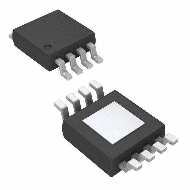
| 供应商器件封装 | 8-SOIC N |
| 其它名称 | CS51411EDR8GOSDKR |
| 包装 | Digi-Reel® |
| 同步整流器 | 无 |
| 安装类型 | 表面贴装 |
| 封装/外壳 | 8-SOIC(0.154",3.90mm 宽) |
| 工作温度 | -40°C ~ 85°C |
| 标准包装 | 1 |
| 电压-输入 | 4.5 V ~ 40 V |
| 电压-输出 | - |
| 电流-输出 | 1.5A |
| 类型 | 降压(降压) |
| 输出数 | 1 |
| 输出类型 | - |
| 频率-开关 | 260kHz |


- 商务部:美国ITC正式对集成电路等产品启动337调查
- 曝三星4nm工艺存在良率问题 高通将骁龙8 Gen1或转产台积电
- 太阳诱电将投资9.5亿元在常州建新厂生产MLCC 预计2023年完工
- 英特尔发布欧洲新工厂建设计划 深化IDM 2.0 战略
- 台积电先进制程称霸业界 有大客户加持明年业绩稳了
- 达到5530亿美元!SIA预计今年全球半导体销售额将创下新高
- 英特尔拟将自动驾驶子公司Mobileye上市 估值或超500亿美元
- 三星加码芯片和SET,合并消费电子和移动部门,撤换高东真等 CEO
- 三星电子宣布重大人事变动 还合并消费电子和移动部门
- 海关总署:前11个月进口集成电路产品价值2.52万亿元 增长14.8%


PDF Datasheet 数据手册内容提取
CS51411, CS51412, CS51413, CS51414 1.5 A, 260 kHz and 520 kHz, Low Voltage Buck Regulators with External Bias or Synchronization http://onsemi.com Capability MARKING DIAGRAMS The CS5141X products are 1.5 A buck regulator ICs. These devices 8 are fixed−frequency operating at 260 kHz and 520 kHz. The regulators 8 5141x use the V2™ control architecture to provide unmatched transient 1 ALYWy (cid:2) response, the best overall regulation and the simplest loop SOIC−8 compensation for today’s high−speed logic. These products D SUFFIX 1 CASE 751 accommodate input voltages from 4.5 V to 40 V. The CS51411 and CS51413 contain synchronization circuitry. The CS51412 and CS51414 have the option of powering the controller from an external 3.3 V to 6.0 V supply in order to improve efficiency, 1 18 18 especially in high input voltage, light load conditions. The on−chip NPN transistor is capable of providing a minimum of CS5141xy 1.5 A of output current, and is biased by an external “boost” capacitor 1 AWLYYWW(cid:2) (cid:2) to ensure saturation, thus minimizing on−chip power dissipation. 18−LEAD DFN MN SUFFIX Protection circuitry includes thermal shutdown, cycle−by−cycle CASE 505 current limiting and frequency foldback. The CS51411 and CS51413 are functionally pin−compatible with the LT1375. The CS51412 and CS51414 are functionally pin−compatible with the LT1376. 5141x =Device Code x = 1, 2, 3 or 4 Features A =Assembly Location L, WL =Wafer Lot • V2 Architecture Provides Ultrafast Transient Response, Improved Y, YY =Year Regulation and Simplified Design W, WW=Work Week • y = E or G 2.0% Error Amp Reference Voltage Tolerance (cid:2) =Pb−Free Package • Switch Frequency Decrease of 4:1 in Short Circuit Conditions Reduces Short Circuit Power Dissipation • BOOST Pin Allows “Bootstrapped” Operation to Maximize ORDERING INFORMATION Efficiency See detailed ordering and shipping information in the package • dimensions section on page 18 of this data sheet. Sync Function for Parallel Supply Operation or Noise Minimization • Shutdown Lead Provides Power−Down Option • 85 (cid:2)A Quiescent Current During Power−Down • Thermal Shutdown • Soft−Start • Pin−Compatible with LT1375 and LT1376 • These Devices are Pb−Free and are RoHS Compliant © Semiconductor Components Industries, LLC, 2013 1 Publication Order Number: May, 2013 − Rev. 21 CS51411/D
CS51411, CS51412, CS51413, CS51414 PIN CONNECTIONS CS51411/3 CS51411/3 CS51412/4 1 8 BOOST VC BOOST 1 18 NC BOOST 1 18 NC VIN VFB VSW GND VVIINN 23 N 1176 VVCFB VVIINN 23 N 1176 VVCFB SHDNB SYNC VIN 4 DF 15 NC VIN 4 DF 15 NC Vsw 5 d 14 NC Vsw 5 d 14 NC a a VSW 6 e 13 GND VSW 6 e 13 GND CS51412/4 L L VSW 7 − 12 NC VSW 7 − 12 NC 1 8 SHDNB 8 18 11 NC BIAS 8 18 11 NC BOOST VC NC 9 10 SYNC NC 9 10 SHDNB VIN VFB VSW GND BIAS SHDNB PACKAGE PIN DESCRIPTION SOIC−8 DFN18 Package Pin # Package Pin # Pin Symbol Function 1 1 BOOST The BOOST pin provides additional drive voltage to the on−chip NPN power transistor. The resulting decrease in switch on voltage increases efficiency. 2 2, 3, 4 VIN This pin is the main power input to the IC. 3 5, 6, 7 VSW This is the connection to the emitter of the on−chip NPN power transistor and serves as the switch output to the inductor. This pin may be subjected to negative voltages during switch off−time. A catch diode is required to clamp the pin voltage in normal operation. This node can stand −1.0 V for less than 50 ns during switch node flyback. 4 8 BIAS The BIAS pin connects to the on−chip power rail and allows the IC to run (CS51412/CS51414) most of its internal circuitry from the regulated output or another low voltage supply to improve efficiency. The BIAS pin is left floating if this feature is not used. 5 This pin provides the synchronization input. (CS51411/CS51413) 10 SYNC 5 10 SHDNB Shutdown_bar input. This is an active−low logical input, TTL compatible, (CS51412/CS51414) (CS51412/CS51414) with an internal pull−up current source. The IC goes into sleep mode, 4 8 drawing less than 85 (cid:2)A when the pin voltage is pulled below 1.0 V. This (CS51411/CS51413) (CS51411/CS51413) pin may be left floating in applications where a shutdown function is not required. 6 13 GND Power return connection for the IC. 7 16 VFB The FB pin provides input to the inverting input of the error amplifier. If VFB is lower than 0.29 V, the oscillator frequency is divided by four, and current limit folds back to about 1 A. These features protect the IC under severe overcurrent or short circuit conditions. 8 17 VC The VC pin provides a connection point to the output of the error amplifier and input to the PWM comparator. Driving of this pin should be avoided because on−chip test circuitry becomes active whenever current exceeding 0.5 mA is forced into the IC. − 9, 11, 12, 14, 15, 18 NC No Connection http://onsemi.com 2
CS51411, CS51412, CS51413, CS51414 PRODUCT SELECTION GUIDE Part Number Frequency Temperature Range Bias/Sync CS51411E 260 kHz −40°C to 85°C Sync CS51411G 260 kHz 0°C to 70°C Sync CS51412E 260 kHz −40°C to 85°C Bias CS51412G 260 kHz 0°C to 70°C Bias CS51413E 520 kHz −40°C to 85°C Sync CS51413G 520 kHz 0°C to 70°C Sync CS51414E 520 kHz −40°C to 85°C Bias CS51414G 520 kHz 0°C to 70°C Bias D1 1N4148 4.5 V − 16 V C1 0.1 (cid:2)F C2 U1 2 1 100 (cid:2)F 3 VIN BOOST VSW 3.3 V L1 4 Shutdown SHDNB 15 (cid:2)H CS51411/3 R1 5 D3 205 C3 SYNC SYNC 100 (cid:2)F 1N5821 VC GND VFB 8 6 7 R2 127 C4 0.1 (cid:2)F Figure 1. Application Diagram, 4.5 V − 16 V to 3.3 V @ 1.0 A Converter MAXIMUM RATINGS Rating Value Unit Operating Junction Temperature Range, TJ −40 to 150 °C Lead Temperature Soldering: Reflow for Leaded: (SMD styles only) (Note 1) 230 peak Reflow for Pb−Free: (SMD styles only) (Note 2) 260 peak °C (Note 3) Storage Temperature Range, TS −65 to +150 °C ESD Damage Threshold (Human Body Model) 2.0 kV Stresses exceeding Maximum Ratings may damage the device. Maximum Ratings are stress ratings only. Functional operation above the Recommended Operating Conditions is not implied. Extended exposure to stresses above the Recommended Operating Conditions may affect device reliability. 1. 60−150 second above 183°C, 30 second maximum at peak. 2. 60−150 second above 217°C, 40 second maximum at peak. 3. +5°C/0°C allowable conditions, applies to both Pb and Pb−Free Devices. http://onsemi.com 3
CS51411, CS51412, CS51413, CS51414 MAXIMUM RATINGS Pin Name VMax VMIN ISOURCE ISINK VIN 40 V −0.3 V N/A 4.0 A BOOST 40 V −0.3 V N/A 100 mA VSW 40 V −0.6 V/−1.0 V, t < 50 ns 4.0 A 10 mA VC 7.0 V −0.3 V 1.0 mA 1.0 mA SHDNB 7.0 V −0.3 V 1.0 mA 1.0 mA SYNC 7.0 V −0.3 V 1.0 mA 1.0 mA BIAS 7.0 V −0.3 V 1.0 mA 50 mA VFB 7.0 V −0.3 V 1.0 mA 1.0 mA GND 7.0 V −0.3 V 50 mA 1.0 mA ELECTRICAL CHARACTERISTICS (−40°C < TJ < 125°C (CS51411E/2E/3E/4E); −40°C < TA < 85°C (CS51411E/2E/3E/4E); 0°C < TA < 70°C (CS51411G/2G/3G/4G), 4.5 V< VIN < 40 V; unless otherwise specified.) Characteristic Test Conditions Min Typ Max Unit Oscillator Operating Frequency CS51411/CS51412 224 260 296 kHz Operating Frequency CS51413/CS51414 446 520 594 kHz Frequency Line Regulation − − 0.05 0.15 %/V Maximum Duty Cycle − 85 90 95 % VFB Frequency Foldback Threshold − 0.29 0.32 0.36 V PWM Comparator Slope Compensation Voltage CS51411/CS51412, Fix VFB, (cid:3)VC/(cid:3)TON 8.0 17 26 mV/(cid:2)s CS51413/CS51414 25 50 75 mV/(cid:2)s Minimum Output Pulse Width CS51411/CS51412, VFB to VSW − 150 300 ns CS51413/CS51414, VFB to VSW − − 230 ns Power Switch Current Limit VFB > 0.36 V 1.6 2.3 3.0 A Foldback Current VFB < 0.29 V 0.9 1.5 2.1 A Saturation Voltage IOUT = 1.5 A, VBOOST = VIN + 2.5 V 0.4 0.7 1.0 V Current Limit Delay (Note 4) − 120 160 ns Error Amplifier Internal Reference Voltage − 1.244 1.270 1.296 V Reference PSRR (Note 4) − 40 − dB FB Input Bias Current − − 0.02 0.1 (cid:2)A Output Source Current VC = 1.270 V, VFB = 1.0 V 15 25 35 (cid:2)A Output Sink Current VC = 1.270 V, VFB = 2.0 V 15 25 35 (cid:2)A Output High Voltage VFB = 1.0 V 1.39 1.46 1.53 V Output Low Voltage VFB = 2.0 V 5.0 20 60 mV Unity Gain Bandwidth (Note 4) − 500 − kHz Open Loop Amplifier Gain (Note 4) − 70 − dB Amplifier Transconductance (Note 4) − 6.4 − mA/V 4. Guaranteed by design, not 100% tested in production. http://onsemi.com 4
CS51411, CS51412, CS51413, CS51414 ELECTRICAL CHARACTERISTICS (−40°C < TJ < 125°C (CS51411E/2E/3E/4E); −40°C < TA < 85°C (CS51411E/2E/3E/4E); 0°C < TA < 70°C (CS51411G/2G/3G/4G), 4.5 V< VIN < 40 V; unless otherwise specified.) Characteristic Test Conditions Min Typ Max Unit Sync Sync Frequency Range CS51411/CS51412 305 − 470 kHz Sync Frequency Range CS51413/CS51414 575 − 880 kHz Sync Pin Bias Current VSYNC = 0 V − 0.1 0.2 (cid:2)A VSYNC = 5.0 V 250 360 460 (cid:2)A Sync Threshold Voltage − 1.0 1.5 1.9 V Shutdown Shutdown Threshold Voltage ICC = 2 mA 1.0 1.3 1.6 V Shutdown Pin Bias Current VSHDNB = 0 V 0.14 5.00 35 (cid:2)A Thermal Shutdown Overtemperature Trip Point (Note 5) 175 185 195 °C Thermal Shutdown Hysteresis (Note 5) − 42 − °C General Quiescent Current ISW = 0 A − − 6.25 mA Shutdown Quiescent Current VSHDNB = 0 V − 20 85 (cid:2)A Boost Operating Current VBOOST − VSW = 2.5 V 6.0 15 40 mA/A Minimum Boost Voltage (Note 5) − − 2.5 V Startup Voltage − 2.2 3.3 4.4 V Minimum Output Current − − 7.0 12 mA 5. Guaranteed by design, not 100% tested in production. http://onsemi.com 5
CS51411, CS51412, CS51413, CS51414 SHDNB SYNC VIN 5.0 (cid:2)A Shutdown Comparator 2.9 V LDO BIAS Voltage + Artificial Oscillator Thermal Regulator − Ramp Shutdown BOOST + 1.3 V − Output S Q Driver R VSW ∑ + Current − Limit Com- parator PWM Com- + IREF 1.46 V parator − − VFB − + + 0.32 V + Frequency IFOLDBACK GND − and Current + Limit Foldback 1.270 V − Error Amplifier VC Figure 2. Block Diagram http://onsemi.com 6
CS51411, CS51412, CS51413, CS51414 APPLICATIONS INFORMATION THEORY OF OPERATION cycle modulation to occur. Actual oscilloscope waveforms V2 Control taken from the converter show the switch node VSWITCH, The CS5141X family of buck regulators utilizes a V2 the error signal VC and the feedback signal VFB (AC control technique and provides a high level of integration to component only) are shown in Figure 5. enable high power density design optimization. Every pulse width modulated controller configures basic S1 L1 control elements such that when connected to the feedback VIN VO signal of a power converter, sufficient loop gain and R1 Duty Cycle C1 bandwidth is available to regulate the voltage set point D1 against line and load variations. The arrangement of these elements differentiates a voltage mode, or a current mode Buck Controller controller from a V2 device. Figure 3 illustrates the basic architecture of a V2 Slope Comp controller. Oscillator + FFB Error Amplifier − Latch S R + Latch/Drive PWM Switch R2 Z2 VREF + SFB − VC − VFB Z1 VO PWM Com- + VREF parator + − Error Amplifier Clock V2 Control Ramp V2 Control Figure 3. V2 Control Figure 4. Buck Converter with V2 Control In common with V mode or I mode, the feedback signal is compared with a reference voltage to develop an error signal which is fed to one input of the PWM. The second input to the PWM, however, is neither a fixed voltage ramp nor the switch current, but rather the feedback signal from VVSSWWIITTCCHH the output of the converter. This feedback signal provides both DC information as well as AC information (the control ramp) for the converter to regulate its set point. The control architecture is known as V2 since both PWM inputs are derived from the converter’s output voltage. This is a little VC misleading because the control ramp is typically generated VFB from current information present in the converter. The feedback signal from the buck converter shown in Figure 4 is processed in one of two ways before being routed to the inputs of the PWM comparator. The Fast Feedback path (FFB) adds slope compensation to the feedback signal before passing it to one input of the PWM. The Slow Figure 5. Feedback path (SFB) compares the original feedback signal against a DC reference. The error signal generated at the In the event of a load transient, the FFB signal changes output of the error amplifier VC is filtered by a low faster, in relation to the filtered SFB signal, causing duty frequency pole before being routed to the second input of the cycle modulation to occur. By this means the converter’s PWM. Each switch cycle is initiated (S1 on), when the transient response time is independent of the error amplifier output latch is set by the oscillator. Each switch cycle bandwidth. The error amplifier is used here to ensure terminates (S1 off), when the FFB signal (AC plus output excellent DC accuracy. DC) exceeds SFB (error DC), and the output latch is reset. In order for the controller to operate optimally, a stable In the event of a load transient, the FFB signal changes ramp is required at the feedback pin. faster, in relation to the filtered SFB signal, causing duty http://onsemi.com 7
CS51411, CS51412, CS51413, CS51414 Control Ramp Generation In original V2 designs, the control ramp VCR was VIN VOUT generated from the converter’s output ripple. Using a current derived ramp provides the same benefits as current mode, R C namely input feed forward, single pole output filter compensation and fast feedback following output load transients. Typically a tantalum or organic polymer capacitor is selected having a sufficiently large ESR component, relative to its capacitive and ESL ripple contributions, to ensure the control ramp was sensing VFB inductor current and its amplitude was sufficient to maintain loop stability. This technique is illustrated in Figure 6. Figure 7. Control Ramp Generated from DCR Inductor Sensing VIN VOUT L Cesr C VFB Figure 6. Control Ramp Generated from Output Advances in multilayer ceramic capacitor technology are such that MLCC’s can provide a cost effective filter solution for low voltage (< 12 V), high frequency converters (>200 kHz). For example, a 10 (cid:2)F MLCC 16 V in a 805 SMT package has an ESR of 2 m(cid:4) and an ESL of Figure 8. 100 nH. Using several MLCC’s in parallel, connected to power and ground planes on a PCB with multiple vias, can Ramp generation using a voltage feed forward technique provide a “near perfect” capacitor. Using this technique, is illustrated in Figure 9. output switching ripple below 10 mV can be readily obtained since parasitic ESR and ESL ripple contributions are nil. In this case, the control ramp is generated elsewhere VIN VOUT in the circuit. Rf CZ Ramp generation using dcr inductor current sensing, where the L/DCR time constant of the output inductor is matched with the CR time constant of the integrating Cf network, is shown in Figure 7. The converter’s transient response following a 1 A step load is shown in Figure 8. This transient response is indicative of a closed loop in excess of 10 kHz having good gain and phase margin in the frequency VFB domain. Also note the amplitude of output switching ripple provided by just two 10 (cid:2)F MLCC’s. Figure 9. Control Ramp from Voltage Feed Forward http://onsemi.com 8
CS51411, CS51412, CS51413, CS51414 Some representative efficiency data is shown in Figure 10. 100 80 %) Y ( 60 C N E CI 40 FI F E Vin = 5.5 V, Vout= 3.3 V 20 Vin = 7.5 V, Vout = 5.0 V Vin = 15V, Vout = 12 V 0 0 500 1000 1500 Figure 11. A CS51411 Buck Regulator is Synced by an IOUT, OUTPUT CURRENT (mA) External 350 kHz Pulse Signal Figure 10. Efficiency versus Output Current Power Switch and Current Limit More detailed information is available in the ON The collector of the built−in NPN power switch is Semiconductor application note AND8276/D on V2 and the connected to the VIN pin, and the emitter to the VSW pin. CS5141x demonstration board number. When the switch turns on, the VSW voltage is equal to the V minus switch Saturation Voltage. In the buck regulator, IN Error Amplifier the V voltage swings to one diode drop below ground SW The CS5141X has a transconductance error amplifier, when the power switch turns off, and the inductor current is whose noninverting input is connected to an Internal commutated to the catch diode. Due to the presence of high Reference Voltage generated from the on−chip regulator. The pulsed current, the traces connecting the V pin, inductor SW inverting input connects to the V pin. The output of the FB and diode should be kept as short as possible to minimize the error amplifier is made available at the V pin. A typical C noise and radiation. For the same reason, the input capacitor frequency compensation requires only a 0.1 (cid:2)F capacitor should be placed close to the V pin and the anode of the IN connected between the V pin and ground, as shown in C diode. Figure 1. This capacitor and error amplifier’s output The saturation voltage of the power switch is dependent resistance (approximately 8.0 M(cid:4)) create a low frequency on the switching current, as shown in Figure 12. pole to limit the bandwidth. Since V2 control does not require a high bandwidth error amplifier, the frequency 0.7 compensation is greatly simplified. The VC pin is clamped below Output High Voltage. This 0.6 allows the regulator to recover quickly from overcurrent or 0.5 short circuit conditions. V) Oscillator and Sync Feature (CS51411 and CS51413 only) (W0.4 S The on−chip oscillator is trimmed at the factory and requires V no external components for frequency control. The high − N0.3 VI switching frequency allows smaller external components to be 0.2 used, resulting in a board area and cost savings. The tight frequency tolerance simplifies magnetic components election. 0.1 The switching frequency is reduced to 25% of the nominal value when the V pin voltage is below Frequency Foldback 0 FB 0 0.5 1.0 1.5 Threshold. In short circuit or overload conditions, this reduces SWITCHING CURRENT (A) the power dissipation of the IC and external components. Figure 12. The Saturation Voltage of the Power Switch An external clock signal can sync CS51411/CS51414 to a Increases with the Conducting Current higher frequency. The rising edge of the sync pulse turns on the power switch to start a new switching cycle, as shown in Members of the CS5141X family contain pulse−by−pulse Figure 11. There is approximately 0.5 (cid:2)s delay between the current limiting to protect the power switch and external rising edge of the sync pulse and rising edge of the V pin components. When the peak of the switching current reaches SW voltage. The sync threshold is TTL logic compatible, and duty the Current Limit, the power switch turns off after the cycle of the sync pulses can vary from 10% to 90%. The Current Limit Delay. The switch will not turn on until the frequency foldback feature is disabled during the sync mode. next switching cycle. The current limit threshold is http://onsemi.com 9
CS51411, CS51412, CS51413, CS51414 independent of switching duty cycle. The maximum load where: current, given by the following formula under continuous V = diode forward voltage. F conduction mode, is less than the Current Limit due to the The anode of the diode can be connected to any DC voltage ripple current. other than the regulated output voltage. However, the IO(MAX)(cid:2)ILIM(cid:3)VO(VIN(cid:3)VO) maAxsim shuomw vno ilnta Fgieg uorne t1h4e ,B thOeO BSOTO pSinT sphianl lc nuorrte enxt cineecdlu 4d0e sV a. 2(L)(VIN)(fs) constant 7.0 mA predriver current and base current where: proportional to switch conducting current. A detailed f = switching frequency, S discussion of this current is conducted in Thermal I = current limit threshold, LIM Consideration section. A 0.1 (cid:2)F capacitor is usually adequate V = output voltage, O for maintaining the Boost pin voltage during the on time. V = input voltage, IN L = inductor value. BIAS Pin (CS51412 and CS51414 Only) When the regulator runs undercurrent limit, the The BIAS pin allows a secondary power supply to bias the subharmonic oscillation may cause low frequency control circuitry of the IC. The BIAS pin voltage should be oscillation, as shown in Figure 13. Similar to current mode between 3.3 V and 6.0 V. If the BIAS pin voltage falls below control, this oscillation occurs at the duty cycle greater than that range, use a diode to prevent current drain from the 50% and can be alleviated by using a larger inductor value. BIAS pin. Powering the IC with a voltage lower than the The current limit threshold is reduced to Foldback Current regulator’s input voltage reduces the IC power dissipation when the FB pin falls below Foldback Threshold. This and improves energy transfer efficiency. feature protects the IC and external components under the power up or overload conditions. 30 A)25 m T ( N E 20 R R U C15 N PI T 10 S O O B 5 0 0 0.5 1.0 1.5 SWITCHING CURRENT (A) Figure 14. The Boost Pin Current Includes 7.0 mA Predriver Current and Base Current when the Switch is Turned On. The Beta Decline of the Power Switch Figure 13. The Regulator in Current Limit Further Increases the Base Current at High BOOST Pin Switching Current The BOOST pin provides base driving current for the Shutdown power switch. A voltage higher than V provides required IN The internal power switch will not turn on until the V headroom to turn on the power switch. This in turn reduces IN pin rises above the Startup Voltage. This ensures no IC power dissipation and improves overall system switching until adequate supply voltage is provided to the efficiency. The BOOST pin can be connected to an external boost−strapping circuit which typically uses a 0.1 (cid:2)F capacitor IC. The IC transitions to sleep mode when the SHDNB pin is pulled low. In sleep mode, the internal power switch and a 1N914 or 1N4148 diode, as shown in Figure 1. When the transistor remains off and supply current is reduced to the power switch is turned on, the voltage on the BOOST pin is Shutdown Quiescent Current value (20 (cid:2)A typical). This pin equal to has an internal pull-up current source, so defaults to high VBOOST(cid:2)VIN(cid:4)VO(cid:3)VF (enabled) state when not connected. http://onsemi.com 10
CS51411, CS51412, CS51413, CS51414 VIN where: V = V pin steady−state voltage, which is approximately C C Q2 equal to error amplifier’s reference voltage. I1 To internal CCOMP = Compensation capacitor connected to the VC pin (cid:2)5(cid:2)A bias rails ISOURCE = Output Source Current of the error amplifier. Using a 0.1 (cid:2)F C , the calculation shows a T over COMP SS SHDNB 20k Q1 5.0 ms which is adequate to avoid any current stresses. Figure 16 shows the gradual rise of the V , V and envelope D1 C O 8V 0k of the VSW during power up. There is no voltage overshoot 8 (a) after the output voltage reaches the regulation. If the supply voltage rises slower than the V pin, output voltage may C 0.65V overshoot. SHDNB SHDNB Z1 (b) 2V to 5V (c) Figure 15. SHDNB pin equivalent internal circuit (a) and practical interface examples (b), (c). Figure 15(a) depicts the SHDNB pin equivalent internal circuit. If the pin is open, current source I1 flows into the base of Q1, turning both Q1 and Q2 on. In turn, Q2 collector current enables the various internal power rails. In Figure 15(b), a standard logic gate is used to pull the pin low by shunting I1 to ground, which places the IC in sleep (shutdown) mode. Note that, when the gate output is logical Figure 16. The Power Up Transition of CS5141X high, the voltage at the SHDNB pin will rise to the internal Regulator clamp voltage of 8 V. This level exceeds the maximum output rating for most common logic families. Protection Short Circuit Zener diode Z1 permits the pin voltage to rise high enough When the V pin voltage drops below Foldback FB to enable the IC, but remain less than the gate output voltage Threshold, the regulator reduces the peak current limit by rating. In Figure 15(c), a single open-collector general- 40% and switching frequency to 1/4 of the nominal purpose NPN transistor is used to pull the pin low. Since frequency. These features are designed to protect the IC and transistors generally have a maximum collector voltage external components during overload or short circuit rating in excess of 8 V, the protection Zener diode in conditions. In those conditions, peak switching current is Figure 15(b) is not required. clamped to the current limit threshold. The reduced switching frequency significantly increases the ripple Startup current, and thus lowers the DC current. The short circuit can During power up, the regulator tends to quickly charge up cause the minimum duty cycle to be limited by Minimum the output capacitors to reach voltage regulation. This gives Output Pulse Width. The foldback frequency reduces the rise to an excessive in−rush current which can be detrimental minimum duty cycle by extending the switching cycle. This to the inductor, IC and catch diode. In V2 control, the protects the IC from overheating, and also limits the power compensation capacitor provides Soft−Start with no need that can be transferred to the output. The current limit for extra pin or circuitry. During the power up, the Output foldback effectively reduces the current stress on the Source Current of the error amplifier charges the inductor and diode. When the output is shorted, the DC compensation capacitor which forces V pin and thus output C current of the inductor and diode can approach the current voltage ramp up gradually. limit threshold. Therefore, reducing the current limit by 40% The Soft−Start duration can be calculated by can result in an equal percentage drop of the inductor and TSS(cid:2)VC(cid:5)CCOMP diode current. The short circuit waveforms are captured in ISOURCE http://onsemi.com 11
CS51411, CS51412, CS51413, CS51414 Figure 17, and the benefit of the foldback frequency and where: current limit is self−evident. I = DC switching current. S When the power switch turns on, the saturation voltage and conduction current contribute to the power loss of a non−ideal switch. The power loss can be quantified as WSAT(cid:2) VO (cid:5)IS(cid:5)VSAT VIN where: V = saturation voltage of the power switch which is SAT shown in Figure 12. The switching loss occurs when the switch experiences both high current and voltage during each switch transition. This regulator has a 30 ns turn−off time and associated power loss is equal to WS(cid:2)IS(cid:5)VIN(cid:5)30ns(cid:5)fS 2 The turn−on time is much shorter and thus turn−on loss is Figure 17. In Short Circuit, the Foldback Current and not considered here. Foldback Frequency Limit the Switching Current to Protect the IC, Inductor and Catch Diode The total power dissipated by the IC is sum of all the above WIC(cid:2)WQ(cid:4)WDRV(cid:4)WBASE(cid:4)WSAT(cid:4)WS Thermal Considerations The IC junction temperature can be calculated from the A calculation of the power dissipation of the IC is always ambient temperature, IC power dissipation and thermal necessary prior to the adoption of the regulator. The current resistance of the package. The equation is shown as follows, drawn by the IC includes quiescent current, predriver TJ(cid:2)WIC(cid:5)R(cid:5)JA(cid:4)TA current, and power switch base current. The quiescent The maximum IC junction temperature shall not exceed current drives the low power circuits in the IC, which 125°C to guarantee proper operation and avoid any damages include comparators, error amplifier and other logic blocks. to the IC. Therefore, this current is independent of the switching current and generates power equal to Using the BIAS Pin WQ(cid:2)VIN(cid:5)IQ The efficiency savings in using the BIAS pin is most where: notable at low load and high input voltage as will be I = quiescent current. explained below. Q Figure 18 will help to understand the increase in efficiency The predriver current is used to turn on/off the power when the BIAS pin is used. The circuitry shown is not the switch and is approximately equal to 12 mA in worst case. actual implementation, but is useful in the explanation. During steady state operation, the IC draws this current from the Boost pin when the power switch is on and then receives it from the VIN pin when the switch is off. The predriver BIAS P1 Internal current always returns to the V pin. Since the predriver BIAS SW current goes out to the regulator’s output even when the power switch is turned off, a minimum load is required to prevent overvoltage in light load conditions. If the Boost pin voltage is equal to V + V when the switch is on, the power IN O dissipation due to predriver current can be calculated by Vin P2 WDRV(cid:2)12mA(cid:5)(VIN(cid:3)VO(cid:4)VO2) VIN The base current of a bipolar transistor is equal to collector current divided by beta of the device. Beta of 60 is used here Figure 18. to estimate the base current. The Boost pin provides the base current when the transistor needs to be on. Internal bias to the IC can be supplied via the Vin pin or the The power dissipated by the IC due to this current is BIAS pin. When the BIAS pin is low, the logic turns P2 on and current is routed to the internal bias circuitry from the WBASE(cid:2)VVOIN2(cid:5)6IS0 Vin pin. Conversely, when the BIAS pin is high, the logic http://onsemi.com 12
CS51411, CS51412, CS51413, CS51414 turns P1 on and current is routed to the internal bias circuitry from the BIAS pin. Here is an example of the power savings: The input voltage range for V is 4.5 V to 40 V. The input in voltage range for BIAS is 3.3 V to 6 V. The quiescent current specification is 3 mA (min), 4 mA (typ), and 6.25 mA (max). Using a typical battery voltage of 14 V and the typical quiescent current number of 4 mA, the power would be: P(cid:2)V(cid:5)I(cid:2)14(cid:5)4e−3(cid:2)56mW We’ll assume the BIAS pin is connected to an external regulator at 5 V instead of the output voltage. The BIAS pin would normally be connected to the output voltage, but adding an added switching regulator efficiency number here would cloud this example. Now the internal BIAS circuitry is being powered via 5 V. The resulting on chip power being dissipated is: Figure 19. Input Voltage Ripple in a Buck Converter P(cid:2)V(cid:5)I(cid:2)5(cid:5)4e−3(cid:2)21mW To calculate the RMS current, multiply the load current The power savings is 35 mW. with the constant given by Figure 20 at each duty cycle. It is Now, to demonstrate more notable savings using the a common practice to select the input capacitor with an RMS maximum battery input voltage of 40 V, the maximum current rating more than half the maximum load current. If quiescent current of 6.25 mA, and the lowest allowed BIAS multiple capacitors are paralleled, the RMS current for each voltage for proper operation of 3.3 V; capacitor should be the total current divided by the number Powered from V : in of capacitors. P(cid:2)40(cid:5)6.25e−3(cid:2)250mW 0.6 Powered from the BIAS pin: P(cid:2)3.3(cid:5)6.25e−3(cid:2)21mW 0.5 The power savings is 229 mW. 0.4 Minimum Load Requirement As pointed out in the previous section, a minimum load is )O XI0.3 required for this regulator due to the predriver current (S feeding the output. Placing a resistor equal to V divided by M O R0.2 12 mA should prevent any voltage overshoot at light load I conditions. Alternatively, the feedback resistors can be 0.1 valued properly to consume 12 mA current. 0 0 0.2 0.4 0.6 0.8 1.0 COMPONENT SELECTION DUTY CYCLE Input Capacitor Figure 20. Input Capacitor RMS Current can be In a buck converter, the input capacitor witnesses pulsed Calculated by Multiplying Y Value with Maximum Load current with an amplitude equal to the load current. This Current at any Duty Cycle pulsed current and the ESR of the input capacitors determine Selecting the capacitor type is determined by each the V ripple voltage, which is shown in Figure 19. For V design’s constraint and emphasis. The aluminum IN IN ripple, low ESR is a critical requirement for the input electrolytic capacitors are widely available at lowest cost. capacitor selection. The pulsed input current possesses a Their ESR and Equivalent Series Inductor (ESL) are significant AC component, which is absorbed by the input relatively high. Multiple capacitors are usually paralleled to capacitors. achieve lower ESR. In addition, electrolytic capacitors The RMS current of the input capacitor can be calculated usually need to be paralleled with a ceramic capacitor for using: filtering high frequency noises. The OS−CON are solid (cid:6) aluminum electrolytic capacitors, and therefore has a much IRMS(cid:2)IO D(1(cid:3)D) lower ESR. Recently, the price of the OS−CON capacitors where: has dropped significantly so that it is now feasible to use D = switching duty cycle which is equal to VO/VIN. them for some low cost designs. Electrolytic capacitors are I = load current. O http://onsemi.com 13
CS51411, CS51412, CS51413, CS51414 physically large, and not used in applications where the size, and especially height is the major concern. Ceramic capacitors are now available in values over 10 (cid:2)F. Since the ceramic capacitor has low ESR and ESL, a single ceramic capacitor can be adequate for both low frequency and high frequency noises. The disadvantage of ceramic capacitors are their high cost. Solid tantalum capacitors can have low ESR and small size. However, the reliability of the tantalum capacitor is always a concern in the application where the capacitor may experience surge current. Output Capacitor In a buck converter, the requirements on the output capacitor are not as critical as those on the input capacitor. The current to the output capacitor comes from the inductor and thus is triangular. In most applications, this makes the Figure 22. The Output Voltage Ripple Using One 100 (cid:2)F RMS ripple current not an issue in selecting output POSCAP Capacitor capacitors. The output ripple voltage is the sum of a triangular wave caused by ripple current flowing through ESR, and a square wave due to ESL. Capacitive reactance is assumed to be small compared to ESR and ESL. The peak−to−peak ripple current of the inductor is: IP(cid:3)P(cid:2)VO(VIN(cid:3)VO) (VIN)(L)(fS) V , the output ripple due to the ESR, is equal RIPPLE(ESR) to the product of I and ESR. The voltage developed P−P across the ESL is proportional to the di/dt of the output capacitor. It is realized that the di/dt of the output capacitor is the same as the di/dt of the inductor current. Therefore, when the switch turns on, the di/dt is equal to (V − V )/L, IN O and it becomes V /L when the switch turns off. The total O ripple voltage induced by ESL can then be derived from Figure 23. The Output Voltage Ripple Using VRIPPLE(ESL)(cid:2)ESL(VIN)(cid:4)ESL(VIN(cid:3)VO)(cid:2)ESL(VIN) One 100 (cid:2)F OS−CON L L L The total output ripple is the sum of the V and RIPPLE(ESR) V . RIPPLE(ESR) Figure 24. The Output Voltage Ripple Using One 100 (cid:2)F Tantalum Capacitor Figure 21. The Output Voltage Ripple Using Two 10 (cid:2)F Ceramic Capacitors in Parallel http://onsemi.com 14
CS51411, CS51412, CS51413, CS51414 Figure 21 to Figure 24 show the output ripple of a 5.0 V The worse case of the diode average current occurs during to 3.3 V/500 mA regulator using 22 (cid:2)H inductor and various maximum load current and maximum input voltage. For the capacitor types. At the switching frequency, the low ESR diode to survive the short circuit condition, the current rating and ESL make the ceramic capacitors behave capacitively of the diode should be equal to the Foldback Current Limit. as shown in Figure 21. Additional paralleled ceramic See Table 1 for Schottky diodes from ON Semiconductor capacitors will further reduce the ripple voltage, but which are suggested for CS5141X regulator. inevitably increase the cost. “POSCAP”, manufactured by Inductor Selection SANYO, is a solid electrolytic capacitor. The anode is When choosing inductors, one might have to consider sintered tantalum and the cathode is a highly conductive maximum load current, core and copper losses, component polymerized organic semiconductor. TPC series, featuring height, output ripple, EMI, saturation and cost. Lower low ESR and low profile, is used in the measurement of inductor values are chosen to reduce the physical size of the Figure 22. It is shown that POSCAP presents a good balance inductor. Higher value cuts down the ripple current, core of capacitance and ESR, compared with a ceramic capacitor. losses and allows more output current. For most In this application, the low ESR generates less than 5.0 mV applications, the inductor value falls in the range between of ripple and the ESL is almost unnoticeable. The ESL of the 2.2 (cid:2)H and 22 (cid:2)H. The saturation current ratings of the through−hole OS−CON capacitor give rise to the inductive inductor shall not exceed the I , calculated according to impedance. It is evident from Figure 23 which shows the L(PK) step rise of the output ripple on the switch turn−on and large IL(PK)(cid:2)IO(cid:4)VO(VIN(cid:3)VO) spike on the switch turn−off. The ESL prevents the output 2(fS)(L)(VIN) capacitor from quickly charging up the parasitic capacitor of The DC current through the inductor is equal to the load the inductor when the switch node is pulled below ground current. The worse case occurs during maximum load through the catch diode conduction. This results in the spike current. Check the vendor’s spec to adjust the inductor value associated with the falling edge of the switch node. The D undercurrent loading. Inductors can lose over 50% of package tantalum capacitor used in Figure 24 has the same inductance when it nears saturation. footprint as the POSCAP, but doubles the height. The ESR The core materials have a significant effect on inductor of the tantalum capacitor is apparently higher than the performance. The ferrite core has benefits of small physical POSCAP. The electrolytic and tantalum capacitors provide size, and very low power dissipation. But be careful not to a low−cost solution with compromised performance. The operate these inductors too far beyond their maximum reliability of the tantalum capacitor is not a serious concern ratings for peak current, as this will saturate the core. for output filtering because the output capacitor is usually Powered Iron cores are low cost and have a more gradual free of surge current and voltage. saturation curve. The cores with an open magnetic path, such as rod or barrel, tend to generate high magnetic field Diode Selection radiation. However, they are usually cheap and small. The The diode in the buck converter provides the inductor cores providing a close magnetic loop, such as pot−core and current path when the power switch turns off. The peak toroid, generate low electro−magnetic interference (EMI). reverse voltage is equal to the maximum input voltage. The There are many magnetic component vendors providing peak conducting current is clamped by the current limit of standard product lines suitable for CS5141X. Table 2 lists the IC. The average current can be calculated from: three vendors, their products and contact information. ID(AVG)(cid:2)IO(VIN(cid:3)VO) VIN http://onsemi.com 15
CS51411, CS51412, CS51413, CS51414 Table 1. Part Number VBREAKDOWN (V) IAVERAGE (A) V(F) (V) @ IAVERAGE Package 1N5817 20 1.0 0.45 Axial Lead 1N5818 30 1.0 0.55 Axial Lead 1N5819 40 1.0 0.6 Axial Lead MBR0520 20 0.5 0.385 SOD−123 MBR0530 30 0.5 0.43 SOD−123 MBR0540 40 0.5 0.53 SOD−123 MBRS120 20 1.0 0.55 SMB MBRS130 30 1.0 0.395 SMB MBRS140 40 1.0 0.6 SMB Table 2. Vendor Product Family Web Site Telephone Coiltronics UNI−Pac1/2: SMT, barrel www.coiltronics.com (516) 241−7876 THIN−PAC: SMT, toroid, low profile CTX: Leaded, toroid Coilcraft DO1608: SMT, barrel www.coilcraft.com (800) 322−2645 DS/DT 1608: SMT, barrel, magnetically shielded DO3316: SMT, barrel DS/DT 3316: SMT, barrel, magnetically shielded DO3308: SMT, barrel, low profile Pulse − www.pulseeng.com (619) 674−8100 http://onsemi.com 16
CS51411, CS51412, CS51413, CS51414 R2 U1 7 373 5.0 V − 12 V input 2 VIN VFB 1 C50.1 (cid:2)F D2 1N4148 C1 BOOST 22 (cid:2)F 4 SHDNB CS51411/3 3 5 VSW 15 (cid:2)H L1 SYNC GND VC 1R237 6 8 D1 C6 MBR0520 22 (cid:2) C2 0.1 (cid:2)F −5.0 V output C3 0.01 (cid:2)F C4 R1 50 k 0.1 (cid:2)F Figure 25. Additional Application Diagram, 5.0 V − 12 V to −5.0 V/400 mA Inverting Converter D2 1N4148 D1 1N4148 12 V C1 0.1 (cid:2)F C1 U1 2 4 1 100 (cid:2)F 3 VIN BIAS BOOST VSW 5.0 V L1 Shutdown 5 SHDNB 15 (cid:2)H CS51412/4 R1 D3 373 C3 100 (cid:2)F 1N5821 VC GND VFB 8 6 7 R2 127 C4 0.1 (cid:2)F Figure 26. Additional Application Diagram, 12 V to 5.0 V/1.0 A Buck Converter using the BIAS Pin http://onsemi.com 17
CS51411, CS51412, CS51413, CS51414 ORDERING INFORMATION Device Operating Temperature Range Package Shipping† CS51411ED8G SOIC−8 (Pb−Free) 98 Units/Rail CS51411EDR8G SOIC−8 (Pb−Free) 2500 Tape & Reel CS51411EMNR2G DFN18 (Pb−Free) 2500 Tape & Reel CS51412ED8G SOIC−8 (Pb−Free) 98 Units/Rail CS51412EDR8G SOIC−8 (Pb−Free) 2500 Tape & Reel CS51412EMNR2G DFN18 (Pb−Free) 2500 Tape & Reel −40°C < TA < 85°C CS51413ED8G SOIC−8 (Pb−Free) 98 Units/Rail CS51413EDR8G SOIC−8 (Pb−Free) 2500 Tape & Reel CS51413EMNR2G DFN18 (Pb−Free) 2500 Tape & Reel CS51414ED8G SOIC−8 (Pb−Free) 98 Units/Rail CS51414EDR8G SOIC−8 (Pb−Free) 2500 Tape & Reel CS51414EMNR2G DFN18 (Pb−Free) 2500 Tape & Reel CS51411GD8G SOIC−8 (Pb−Free) 98 Units/Rail CS51411GDR8G SOIC−8 (Pb−Free) 2500 Tape & Reel CS51411GMNR2G DFN18 (Pb−Free) 2500 Tape & Reel CS51412GD8G SOIC−8 (Pb−Free) 98 Units/Rail CS51412GDR8G SOIC−8 (Pb−Free) 2500 Tape & Reel CS51412GMNR2G DFN18 (Pb−Free) 2500 Tape & Reel 0°C < TA < 70°C CS51413GD8G SOIC−8 (Pb−Free) 98 Units/Rail CS51413GDR8G SOIC−8 (Pb−Free) 2500 Tape & Reel CS51413GMNR2G DFN18 (Pb−Free) 2500 Tape & Reel CS51414GD8G SOIC−8 (Pb−Free) 98 Units/Rail CS51414GDR8G SOIC−8 (Pb−Free) 2500 Tape & Reel CS51414GMNR2G DFN18 (Pb−Free) 2500 Tape & Reel †For information on tape and reel specifications, including part orientation and tape sizes, please refer to our Tape and Reel Packaging Specifications Brochure, BRD8011/D. http://onsemi.com 18
CS51411, CS51412, CS51413, CS51414 PACKAGE DIMENSIONS SOIC−8 NB CASE 751−07 ISSUE AK NOTES: −X− 1. DIMENSIONING AND TOLERANCING PER ANSI Y14.5M, 1982. A 2. CONTROLLING DIMENSION: MILLIMETER. 3. DIMENSION A AND B DO NOT INCLUDE MOLD PROTRUSION. 4. MAXIMUM MOLD PROTRUSION 0.15 (0.006) 8 5 PER SIDE. 5. DIMENSION D DOES NOT INCLUDE DAMBAR B S 0.25 (0.010) M Y M PROTRUSION. ALLOWABLE DAMBAR PROTRUSION SHALL BE 0.127 (0.005) TOTAL 1 IN EXCESS OF THE D DIMENSION AT −Y− 4 K 6. M75A1X−I0M1U TMH RMUA T7E51R−IA0L6 CAROEN DOIBTSIOONL.ETE. NEW STANDARD IS 751−07. G MILLIMETERS INCHES DIM MIN MAX MIN MAX C NX 45(cid:3) A 4.80 5.00 0.189 0.197 B 3.80 4.00 0.150 0.157 SEATING PLANE C 1.35 1.75 0.053 0.069 −Z− D 0.33 0.51 0.013 0.020 G 1.27 BSC 0.050 BSC 0.10 (0.004) H 0.10 0.25 0.004 0.010 H D M J J 0.19 0.25 0.007 0.010 K 0.40 1.27 0.016 0.050 M 0 (cid:3) 8 (cid:3) 0 (cid:3) 8 (cid:3) N 0.25 0.50 0.010 0.020 0.25 (0.010)M Z Y S X S S 5.80 6.20 0.228 0.244 SOLDERING FOOTPRINT* 1.52 0.060 7.0 4.0 0.275 0.155 0.6 1.270 0.024 0.050 (cid:7) (cid:8) mm SCALE 6:1 inches *For additional information on our Pb−Free strategy and soldering details, please download the ON Semiconductor Soldering and Mounting Techniques Reference Manual, SOLDERRM/D. PACKAGE THERMAL DATA Parameter SOIC−8 Unit R(cid:5)JC Typical 45 °C/W R(cid:5)JA Typical 165 °C/W http://onsemi.com 19
CS51411, CS51412, CS51413, CS51414 PACKAGE DIMENSIONS DFN18 6x5, 0.5P A CASE 505 NOTES: D ISSUE D 1. DIMENSIONS AND TOLERANCING PER B ASME Y14.5M, 1994. 2. DIMENSIONS IN MILLIMETERS. 3. DIMENSION b APPLIES TO PLATED TERMINAL AND IS MEASURED BETWEEN 0.25 AND 0.30 MM FROM TERMINAL 4. COPLANARITY APPLIES TO THE EXPOSED PIN 1 LOCATION PAD AS WELL AS THE TERMINALS. E MILLIMETERS 2X DIM MIN MAX 0.15 C A 0.80 1.00 A1 0.00 0.05 2X A3 0.20 REF 0.15 C TOP VIEW b 0.18 0.30 D 6.00 BSC D2 3.98 4.28 0.10 C (A3) E 5.00 BSC E2 2.98 3.28 18X A e 0.50 BSC K 0.20 −−− 0.08 C A1 L 0.45 0.65 C SIDE VIEW SEATING PLANE SOLDERING FOOTPRINT D2 e 5.30 18X 18X L 0.75 1 9 1 0.50 E2 PITCH 18X K 18 10 4.19 18X b 0.10 C A B BOTTOM VIEW 18X 0.05 C NOTE 3 0.30 3.24 DIMENSIONS: MILLIMETERS *For additional information on our Pb−Free strategy and soldering details, please download the ON Semiconductor Soldering and Mounting Techniques Reference Manual, SOLDERRM/D. PACKAGE THERMAL DATA Parameter DFN18 Unit R(cid:5)JA Typical 35 °C/W V2 is a trademark of Switch Power, Inc. ON Semiconductor and are registered trademarks of Semiconductor Components Industries, LLC (SCILLC). SCILLC owns the rights to a number of patents, trademarks, copyrights, trade secrets, and other intellectual property. A listing of SCILLC’s product/patent coverage may be accessed at www.onsemi.com/site/pdf/Patent−Marking.pdf. SCILLC reserves the right to make changes without further notice to any products herein. SCILLC makes no warranty, representation or guarantee regarding the suitability of its products for any particular purpose, nor does SCILLC assume any liability arising out of the application or use of any product or circuit, and specifically disclaims any and all liability, including without limitation special, consequential or incidental damages. “Typical” parameters which may be provided in SCILLC data sheets and/or specifications can and do vary in different applications and actual performance may vary over time. All operating parameters, including “Typicals” must be validated for each customer application by customer’s technical experts. SCILLC does not convey any license under its patent rights nor the rights of others. SCILLC products are not designed, intended, or authorized for use as components in systems intended for surgical implant into the body, or other applications intended to support or sustain life, or for any other application in which the failure of the SCILLC product could create a situation where personal injury or death may occur. Should Buyer purchase or use SCILLC products for any such unintended or unauthorized application, Buyer shall indemnify and hold SCILLC and its officers, employees, subsidiaries, affiliates, and distributors harmless against all claims, costs, damages, and expenses, and reasonable attorney fees arising out of, directly or indirectly, any claim of personal injury or death associated with such unintended or unauthorized use, even if such claim alleges that SCILLC was negligent regarding the design or manufacture of the part. SCILLC is an Equal Opportunity/Affirmative Action Employer. This literature is subject to all applicable copyright laws and is not for resale in any manner. PUBLICATION ORDERING INFORMATION LITERATURE FULFILLMENT: N. American Technical Support: 800−282−9855 Toll Free ON Semiconductor Website: www.onsemi.com Literature Distribution Center for ON Semiconductor USA/Canada P.O. Box 5163, Denver, Colorado 80217 USA Europe, Middle East and Africa Technical Support: Order Literature: http://www.onsemi.com/orderlit Phone: 303−675−2175 or 800−344−3860 Toll Free USA/Canada Phone: 421 33 790 2910 Fax: 303−675−2176 or 800−344−3867 Toll Free USA/Canada Japan Customer Focus Center For additional information, please contact your local Email: orderlit@onsemi.com Phone: 81−3−5817−1050 Sales Representative http://onsemi.com CS51411/D 20