ICGOO在线商城 > 电阻器 > 芯片电阻 - 表面安装 > CRCW040222R0JNEDIF
 Datasheet下载
- 型号: CRCW040222R0JNEDIF
- 制造商: Vishay
- 库位|库存: xxxx|xxxx
- 要求:
| 数量阶梯 | 香港交货 | 国内含税 |
| +xxxx | $xxxx | ¥xxxx |
查看当月历史价格
查看今年历史价格
CRCW040222R0JNEDIF产品简介:
ICGOO电子元器件商城为您提供CRCW040222R0JNEDIF由Vishay设计生产,在icgoo商城现货销售,并且可以通过原厂、代理商等渠道进行代购。 CRCW040222R0JNEDIF价格参考。VishayCRCW040222R0JNEDIF封装/规格:芯片电阻 - 表面安装, 22 Ohms ±5% 0.063W, 1/16W Chip Resistor 0402 (1005 Metric) Automotive AEC-Q200, Pulse Withstanding Thick Film。您可以下载CRCW040222R0JNEDIF参考资料、Datasheet数据手册功能说明书,资料中有CRCW040222R0JNEDIF 详细功能的应用电路图电压和使用方法及教程。
Vishay Dale的CRCW040222R0JNEDIF是一款0402封装尺寸的表面贴装芯片电阻,阻值为22Ω,精度±5%(J级),属于CRCW e3系列。该电阻具有良好的稳定性和可靠性,适用于对空间要求严苛且需要稳定电气性能的电子电路。

典型应用场景包括:便携式消费类电子产品(如智能手机、平板电脑、可穿戴设备)中的电源管理、信号调节和电压分压电路;通信设备中的射频模块与接口电路;计算机及外围设备中的主板、内存模块和电源控制单元;工业控制设备中的传感器信号调理和微控制器周边电路;以及汽车电子中的车载信息娱乐系统和车身控制模块等。

由于其小尺寸和SMT封装,特别适合高密度PCB布局和自动化贴片生产。此外,该电阻符合RoHS环保要求,具备良好的耐湿性和温度循环性能,可在较宽的工作温度范围内稳定运行,广泛用于对可靠性和一致性有较高要求的中高端电子制造领域。
| 参数 | 数值 |
| 产品目录 | |
| 描述 | RES 22 OHM 1/16W 5% 0402 SMD |
| 产品分类 | |
| 品牌 | Vishay Dale |
| 数据手册 | |
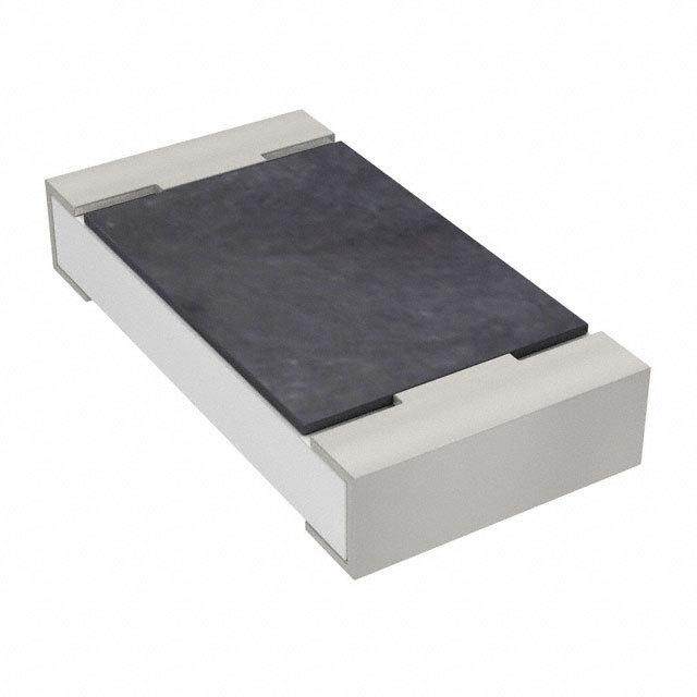
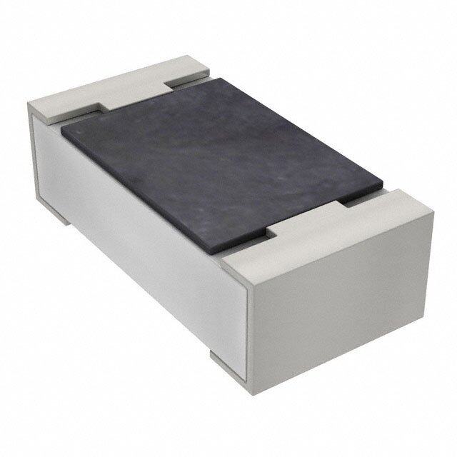
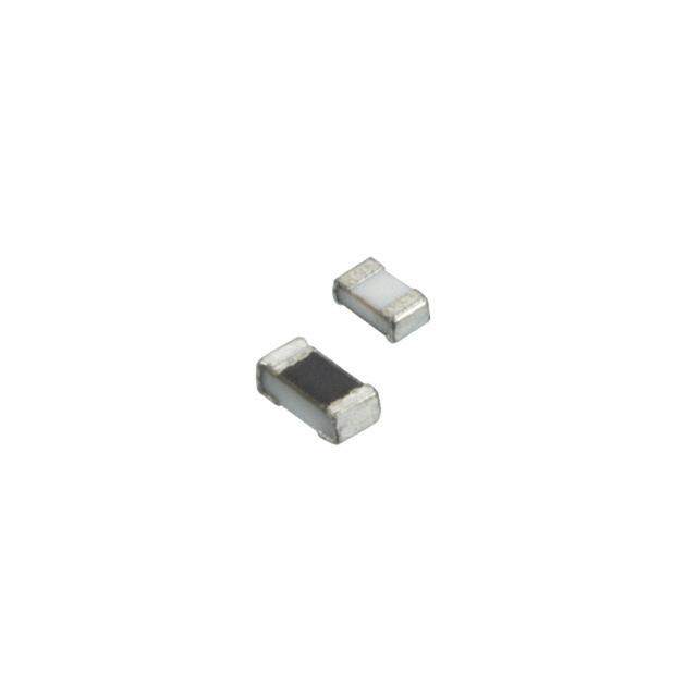
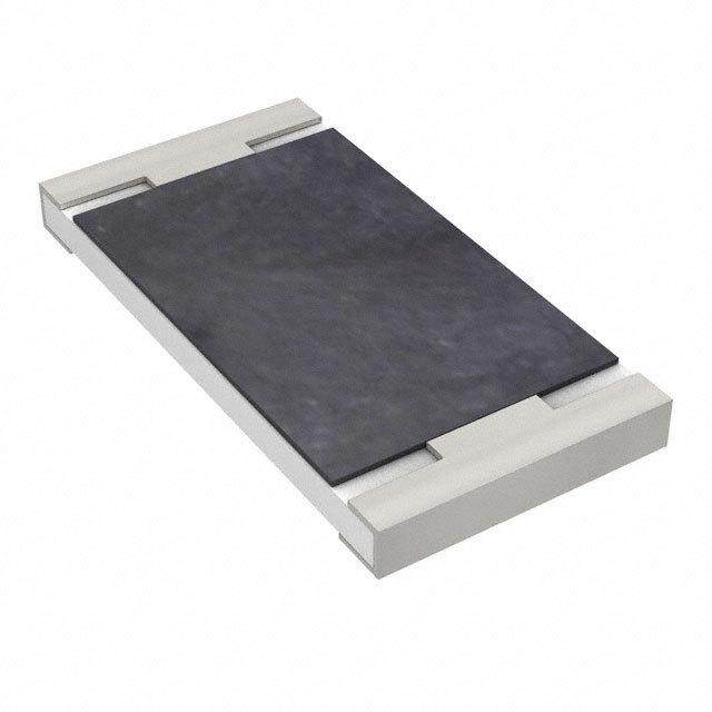
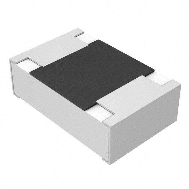
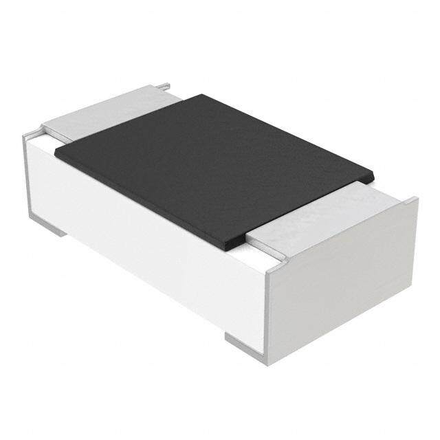
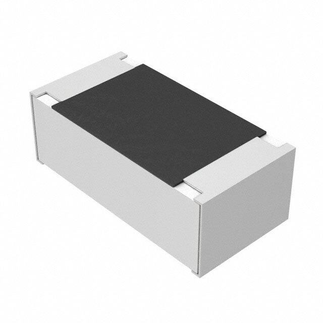
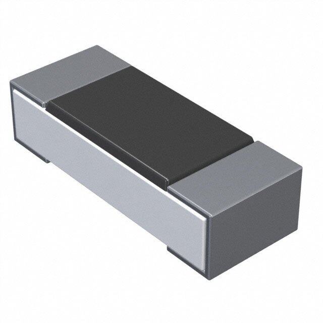
| 产品图片 |
|
| 产品型号 | CRCW040222R0JNEDIF |
| rohs | 无铅 / 符合限制有害物质指令(RoHS)规范要求 |
| 产品系列 | CRCW-IF |
| 供应商器件封装 | 0402(1005 公制) |
| 其它名称 | 541-22ATCT |
| 功率(W) | 0.063W,1/16W |
| 包装 | 剪切带 (CT) |
| 大小/尺寸 | 0.039" 长 x 0.020" 宽(1.00mm x 0.50mm) |
| 容差 | ±5% |
| 封装/外壳 | 0402(1005 公制) |
| 成分 | 厚膜 |
| 标准包装 | 1 |
| 温度系数 | ±200ppm/°C |
| 特性 | 获得 AEC-Q200 汽车认证,防脉冲 |
| 电阻(Ω) | 22 |
| 端子数 | 2 |
| 高度 | 0.016"(0.40mm) |
.jpg)


- 商务部:美国ITC正式对集成电路等产品启动337调查
- 曝三星4nm工艺存在良率问题 高通将骁龙8 Gen1或转产台积电
- 太阳诱电将投资9.5亿元在常州建新厂生产MLCC 预计2023年完工
- 英特尔发布欧洲新工厂建设计划 深化IDM 2.0 战略
- 台积电先进制程称霸业界 有大客户加持明年业绩稳了
- 达到5530亿美元!SIA预计今年全球半导体销售额将创下新高
- 英特尔拟将自动驾驶子公司Mobileye上市 估值或超500亿美元
- 三星加码芯片和SET,合并消费电子和移动部门,撤换高东真等 CEO
- 三星电子宣布重大人事变动 还合并消费电子和移动部门
- 海关总署:前11个月进口集成电路产品价值2.52万亿元 增长14.8%


PDF Datasheet 数据手册内容提取
D/CRCW-IF e3 www.vishay.com Vishay Pulse Proof Thick Film Chip Resistors FEATURES • High pulse performance, up to 10 kW • Stability R/R 1 % for 1000 h at 70 °C • AEC-Q200 qualified • Material categorization: for definitions of compliance please see www.vishay.com/doc?99912 STANDARD ELECTRICAL SPECIFICATIONS LIMITING POWER ELEMENT CASE CASE TEMPERATURE RESISTANCE RATING VOLTAGE TOLERANCE TYPE SIZE SIZE COEFFICIENT RANGE SERIES P U % IMPERIAL METRIC 70 max. ppm/K W AC /DC RMS V ± 5 D10/CRCW0402-IF 0402 RR1005M 0.063 50 ± 200 1.0 to 100K E24 ± 10 ± 5 D11/CRCW0603-IF 0603 RR1608M 0.10 75 ± 200 1.0 to 100K E24 ± 10 ± 5 D12/CRCW0805-IF 0805 RR2012M 0.125 150 ± 200 1.0 to 100K E24 ± 10 ± 5 D25/CRCW1206-IF 1206 RR3216M 0.25 200 ± 200 1.0 to 100K E24 ± 10 ± 5 CRCW1210-IF 1210 RR3225M 0.50 200 ± 200 1.0 to 100K E24 ± 10 ± 5 CRCW2010-IF 2010 RR5025M 0.75 400 ± 200 1.0 to 100K E24 ± 10 ± 5 CRCW2512-IF 2512 RR6332M 1.0 500 ± 200 1.0 to 100K E24 ± 10 Notes • These resistors do not feature a limited lifetime when operated within the limits of rated dissipation, permissible operating voltage, and permissible film temperature. However, the resistance typically increase due to the resistor’s film temperature over operating time, generally known as drift. The drift may exceed the stability requirements of an individual application circuit and thereby limits the functional time. • Marking: See data sheet “Surface Mount Resistor Marking” (document number 20020). • Power rating depends on the max. temperature at the solder point, the component placement density and the substrate material. TECHNICAL SPECIFICATIONS D10/ D11/ D12/ D25/ PARAMETER UNIT CRCW1210-IF CRCW2010-IF CRCW2512-IF CRCW0402-IF CRCW0603-IF CRCW0805-IF CRCW1206-IF Rated dissipation W 0.063 0.1 0.125 0.25 0.5 0.75 1.0 P (1) 70 Operating voltage V 50 75 150 200 200 400 500 U AC /DC max. RMS Insulation voltage V 75 100 200 300 300 300 300 U (1 min) ins Insulation resistance > 109 Operating temperature °C -55 to +155 range Failure rate h-1 < 0.1 x 10⁻⁹ Mass mg 0.65 2 5.5 10 16 25.5 40.5 Note (1) The power dissipation on the resistor generates a temperature rise against the local ambient, depending on the heat flow support of the printe-circuit board (thermal resistance). The rated dissipation applies only if the permitted film temperature of 155 °C is not exceeded. Revision: 17-Mar-15 1 Document Number: 20024 For technical questions, contact: thickfilmchip@vishay.com THIS DOCUMENT IS SUBJECT TO CHANGE WITHOUT NOTICE. THE PRODUCTS DESCRIBED HEREIN AND THIS DOCUMENT ARE SUBJECT TO SPECIFIC DISCLAIMERS, SET FORTH AT www.vishay.com/doc?91000
D/CRCW-IF e3 www.vishay.com Vishay PART NUMBER AND PRODUCT DESCRIPTION Part Number: CRCW08051R00JNEAIF C R C W 0 8 0 5 1 R 0 0 J N E A I F TYPE VALUE TOLERANCE TCR PACKAGING SPECIAL CRCW0402 R = Decimal J = ± 5 % N = ± 200 ppm/K EA, EB, Up to 2 digits CRCW0603 K = Thousand K = ± 10 % EC, ED, IF = Pulse proof CRCW0805 EE, EF, CRCW1206 EG, EH, CRCW1210 EI, EL CRCW2010 CRCW2512 Product Description: D12/CRCW0805-IF 200 1R0 5 % ET1 e3 D12/CRCW0805-IF 200 1R0 5 % ET1 e3 TYPE TCR RESISTANCE VALUE TOLERANCE PACKAGING LEAD (Pb)-FREE D10/CRCW0402-IF ± 200 ppm/K 1R0 = 1 ± 5 % ET1, ET2, e3 = Pure tin D11/CRCW0603-IF 10K = 10 k ± 10 % ET3, ET4, termination finish D12/CRCW0805-IF ET5, ET6, D25/CRCW1206-IF ET7, ET8, CRCW1210-IF ET9, EF4, CRCW2010-IF E02, E67, CRCW2512-IF E82 PACKAGING TYPE CODE QUANTITY CARRIER TAPE WIDTH PITCH REEL DIAMETER ED = ET7 10 000 180 mm/7" D10/CRCW0402-IF 8 mm 2 mm EE = EF4 50 000 330 mm/13" EI = ET2 5000 180 mm/7" ED = ET3 10 000 180 mm/7" 8 mm 2 mm EL = ET4 20 000 285 mm/11.25" D11/CRCW0603-IF EE = ET8 50 000 330 mm/13" EA = ET1 5000 180 mm/7" EB = ET5 10 000 8 mm 4 mm 285 mm/11.25" EC = ET6 20 000 Paper tape acc. to 330 mm/13" IEC 60286-3 EA = ET1 5000 Type 1a 180 mm/7" D12/CRCW0805-IF EB = ET5 10 000 8 mm 4 mm 285 mm/11.25" EC = ET6 20 000 330 mm/13" EA = ET1 5000 180 mm/7" D25/CRCW1206-IF EB = ET5 10 000 8 mm 4 mm 285 mm/11.25" EC = ET6 20 000 330 mm/13" EA = ET1 5000 180 mm/7" CRCW1210-IF EB = ET5 10 000 8 mm 4 mm 285 mm/11.25" EC = ET6 20 000 330 mm/13" CRCW2010-IF EF = E02 4000 Pressed tape 12 mm 4 mm 180 mm/7" acc. to EG = E67 2000 8 mm CRCW2512-IF IEC 60286-3 12 mm 180 mm/7" EH = E82 4000 Type 1b 4 mm Revision: 17-Mar-15 2 Document Number: 20024 For technical questions, contact: thickfilmchip@vishay.com THIS DOCUMENT IS SUBJECT TO CHANGE WITHOUT NOTICE. THE PRODUCTS DESCRIBED HEREIN AND THIS DOCUMENT ARE SUBJECT TO SPECIFIC DISCLAIMERS, SET FORTH AT www.vishay.com/doc?91000
D/CRCW-IF e3 www.vishay.com Vishay DIMENSIONS in millimeters L T2 I b W a H T1 RECOMMENDED SOLDER PAD DIMENSIONS SIZE DIMENSIONS REFLOW WAVE SOLDERING SOLDERING IMPERIAL METRIC L W H T1 T2 a b l a b l 0402 RR1005M 1.0 ± 0.05 0.5 ± 0.05 0.35 ± 0.05 0.25 ± 0.05 0.2 ± 0.1 0.4 0.6 0.5 0603 RR1608M 1.55 + 0.10 0.85 ± 0.1 0.45 ± 0.05 0.3 ± 0.2 0.3 ± 0.2 0.5 0.9 1.0 0.9 0.9 1.0 - 0.05 0805 RR2012M 2.0 + 0.20 1.25 ± 0.15 0.45 ± 0.05 0.3 + 0.20 0.3 ± 0.2 0.7 1.3 1.2 0.9 1.3 1.3 - 0.10 - 0.10 1206 RR3216M 3.2 + 0.10 1.6 ± 0.15 0.55 ± 0.05 0.45 ± 0.2 0.4 ± 0.2 0.9 1.7 2.0 1.1 1.7 2.3 - 0.20 1210 RR3225M 3.2 ± 0.2 2.5 ± 0.2 0.55 ± 0.05 0.45 ± 0.2 0.4 ± 0.2 0.9 2.5 2.0 1.1 2.5 2.2 2010 RR5025M 5.0 ± 0.15 2.5 ± 0.15 0.6 ± 0.1 0.6 ± 0.2 0.6 ± 0.2 1.0 2.5 3.9 1.2 2.5 3.9 2512 RR6332M 6.3 ± 0.2 3.15 ± 0.15 0.6 ± 0.1 0.6 ± 0.2 0.6 ± 0.2 1.0 3.2 5.2 1.2 3.2 5.2 FUNCTIONAL PERFORMANCE Maximum pulse dissipation as a function of the pulse duration, single pulse 100 000 W) wer ( 10 000 221502111200 o P 1206 se 1000 0805 ul 0603 P 0402 100 10 1 0.1 0.01 0.0000010.00001 0.0001 0.001 0.01 0.1 1 10 100 Pulse Duration (s) Maximum pulse load, single pulse; applicable if P 0 and n ≤ 1000 and Û ≤ Ûmax.; for permissible resistance change equivalent to 8000 h operation Revision: 17-Mar-15 3 Document Number: 20024 For technical questions, contact: thickfilmchip@vishay.com THIS DOCUMENT IS SUBJECT TO CHANGE WITHOUT NOTICE. THE PRODUCTS DESCRIBED HEREIN AND THIS DOCUMENT ARE SUBJECT TO SPECIFIC DISCLAIMERS, SET FORTH AT www.vishay.com/doc?91000
D/CRCW-IF e3 www.vishay.com Vishay Maximum pulse dissipation as a function of the pulse duration, continuous pulse loading 100 000 W) wer ( 10 000 221502111200 o P 1206 se 1000 0805 ul 0603 P 0402 100 10 1 0.1 0.01 0.0000010.00001 0.0001 0.001 0.01 0.1 1 10 100 Pulse Duration (s) Maximum pulse load, continuous pulses; applicable if P ≤ P (ϑamb) and Û ≤ Ûmax.; for permissible resistance change equivalent to 8000 h operation V) 2000 (max. 1800 2512 Ûe 1600 ag 2010 olt 1400 V e 1200 s ul P 1000 800 1206/1210 600 400 0805 0603 200 0402 0 10- 6 10- 5 10- 4 10- 3 10- 2 10- 1 1 10 Pulse Duration t (s) i Maximum pulse voltage, single and continuous pulses; applicable if P ≤ Pmax.; for permissible resistance change equivalent to 8000 h operation Revision: 17-Mar-15 4 Document Number: 20024 For technical questions, contact: thickfilmchip@vishay.com THIS DOCUMENT IS SUBJECT TO CHANGE WITHOUT NOTICE. THE PRODUCTS DESCRIBED HEREIN AND THIS DOCUMENT ARE SUBJECT TO SPECIFIC DISCLAIMERS, SET FORTH AT www.vishay.com/doc?91000
D/CRCW-IF e3 www.vishay.com Vishay Single-pulse high voltage overload test 1.2 µs/50 µs EN 140000 4.27 10 000 ge (V) 22501120 k Volta 1000 110228100065 a e 0603 P 0402 100 10 1 1 10 100 1000 10 000 100 000 Resistance Value (Ω) Pulse load rating in accordance to EN 60115-1, 4.27; 1.2 μs/50 μs; 5 pulses at 12 s intervals; for permissible resistance change 1 % Single-pulse high voltage overload test 10 µs/700 µs EN 140000 4.27 10 000 ge (V) 22501120 k Volta 1000 110228100065 a e 0603 P 0402 100 10 1 1 10 100 1000 10 000 100 000 Resistance Value (Ω) Pulse load rating in accordance to EN 60115-1, 4.27; 10 μs/700 μs; 10 pulses at 1 min intervals; for permissible resistance change 1 % Revision: 17-Mar-15 5 Document Number: 20024 For technical questions, contact: thickfilmchip@vishay.com THIS DOCUMENT IS SUBJECT TO CHANGE WITHOUT NOTICE. THE PRODUCTS DESCRIBED HEREIN AND THIS DOCUMENT ARE SUBJECT TO SPECIFIC DISCLAIMERS, SET FORTH AT www.vishay.com/doc?91000
D/CRCW-IF e3 www.vishay.com Vishay Derating %) P(70 n 100 o ati p si s Di d e at R of 50 n o cti a Fr 0 - 50 0 50 70 100 150 Ambient Temperature ϑ (°C) amb TEST PROCEDURES AND REQUIREMENTS REQUIREMENTS PERMISSIBLE IEC PROCEDURE CHANGE (R) EN 60115-1 60082-2 TEST STABILITY CLASS 1 OR BETTER TEST CLAUSE METHOD Stability for product type: 1 to 100 k D/CRCW-IF e3 4.5 - Resistance - ± 5 %; ± 10 % 4.7 - Voltage proof U = 1.4 x U ; 60 s No flashover or breakdown ins 4.13 - Short time overload U = 2.5 x P70 x R 2 x Umax.; ± (0.25 % R + 0.05 ) duration acc. to style Solder bath method; Sn60Pb40; Good tinning ( 95 % covered); non-activated flux; no visible damage (235 ± 5) °C, (2 ± 0.2) s 4.17.2 58 (Td) Solderability Solder bath method; Sn96.5Ag3Cu0.5; Good tinning ( 95 % covered); non-activated flux; no visible damage (245 ± 5) °C, (3 ± 0.3) s (20/- 55/20) °C and 4.8.4.2 - Temperature coefficient ± 200 ppm/K (20/125/20) °C 30 min. at - 55 °C; 30 min. at 125°C 4.19 14 (Na) Rapid change of temperature 5 cycles ± (0.25 % R + 0.05 ) 1000 cycles ± (1 % R + 0.05 ) Revision: 17-Mar-15 6 Document Number: 20024 For technical questions, contact: thickfilmchip@vishay.com THIS DOCUMENT IS SUBJECT TO CHANGE WITHOUT NOTICE. THE PRODUCTS DESCRIBED HEREIN AND THIS DOCUMENT ARE SUBJECT TO SPECIFIC DISCLAIMERS, SET FORTH AT www.vishay.com/doc?91000
D/CRCW-IF e3 www.vishay.com Vishay TEST PROCEDURES AND REQUIREMENTS REQUIREMENTS PERMISSIBLE IEC PROCEDURE CHANGE (R) EN 60115-1 60082-2 TEST STABILITY CLASS 1 OR BETTER TEST CLAUSE METHOD Stability for product type: 1 to 100 k D/CRCW-IF e3 4.23 - Climatic sequence: - 4.23.2 2 (Ba) Dry heat 125 °C; 16 h 55 °C; 90 % RH; 4.23.3 30 (Db) Damp heat, cyclic 24 h; 1 cycle 4.23.4 1 (Aa) Cold - 55 °C; 2 h ± (1 % R + 0.05 ) 4.23.5 13 (M) Low air pressure 1 kPa; (25 ± 10) °C; 1 h 55 °C; 90 % RH; 4.23.6 30 (Db) Damp heat, cyclic 24 h; 5 cycles 4.23.7 - DC load U = P x R 70 U = P70 x R Umax. 1.5 h on; 0.5 h off; 4.25.1 - Endurance at 70 °C 70 °C; 1000 h ± (1 % R + 0.05 ) 70 °C; 8000 h ± (2 % R + 0.1 ) Solder bath method 4.18.2 58 (Td) Resistance to soldering heat ± (0.25 % R + 0.05 ) (260 ± 5) °C; (10 ± 1) s (40 ± 2) °C; 4.24 78 (Cab) Damp heat, steady state ± (1 % R + 0.05 ) (93 ± 3) % RH; 56 days Endurance at upper 4.25.3 - 155 °C; 1000 h ± (1 % R + 0.05 ) category temperature 4.27 - Single pulse high voltage Û = 10 x P70 x R 2 x Umax.; ± (1 % R + 0.05 ) overload, 10 μs/700 μs 10 pulses All tests are carried out in accordance with the following specifications: • EN 60115-1, generic specification • EN 140400, sectional specification • EN 140401-802, detail specification • IEC 60068-2-x, environmental test procedures Packaging of components is done in paper or blister tapes according to IEC 60286-3. Revision: 17-Mar-15 7 Document Number: 20024 For technical questions, contact: thickfilmchip@vishay.com THIS DOCUMENT IS SUBJECT TO CHANGE WITHOUT NOTICE. THE PRODUCTS DESCRIBED HEREIN AND THIS DOCUMENT ARE SUBJECT TO SPECIFIC DISCLAIMERS, SET FORTH AT www.vishay.com/doc?91000
Legal Disclaimer Notice www.vishay.com Vishay Disclaimer ALL PRODUCT, PRODUCT SPECIFICATIONS AND DATA ARE SUBJECT TO CHANGE WITHOUT NOTICE TO IMPROV E RELIABILITY, FUNCTION OR DESIGN OR OTHERWISE. Vishay Intertechnology, Inc., its affiliates, agents, and employees, and all persons acting on its or their behalf (collectively, “Vishay”), disclaim any and all liability for any errors, inaccuracies or incompleteness contained in any datasheet or in any other disclosure relating to any product. Vishay makes no warranty, representation or guarantee regarding the suitability of the products for any particular purpose o r the continuing production of any product. To the maximum extent permitted by applicable law, Vishay disclaims (i) any and all liability arising out of the application or use of any product, (ii) any and all liability, including without limitation special, consequential or incidental damages, and (iii) any and all implied warranties, including warranties of fitness for particular purpose, non-infringement and merchantability. Statements regarding the suitability of products for certain types of applications are based on Vishay’s knowledge of typical requirements that are often placed on Vishay products in generic applications. Such statements are not binding statements about the suitability of products for a particular application. It is the customer’s responsibility to validate that a particular product with the properties described in the product specification is suitable for use in a particular application. Parameters provided in datasheets and / or specifications may vary in different applications and performance may vary over time. All operating parameters, including typical parameters, must be validated for each customer application by the customer’s technical experts. Product specifications do not expand or otherwise modify Vishay’s terms and conditions of purchase, including but not limited to the warranty expressed therein. Except as expressly indicated in writing, Vishay products are not designed for use in medical, life-saving, or life-sustainin g applications or for any other application in which the failure of the Vishay product could result in personal injury or death. Customers using or selling Vishay products not expressly indicated for use in such applications do so at their own risk . Please contact authorized Vishay personnel to obtain written terms and conditions regarding products designed for such applications. No license, express or implied, by estoppel or otherwise, to any intellectual property rights is granted by this documen t or by any conduct of Vishay. Product names and markings noted herein may be trademarks of their respective owners. © 2019 VISHAY INTERTECHNOLOGY, INC. ALL RIGHTS RESERVED Revision: 01-Jan-2019 1 Document Number: 91000