ICGOO在线商城 > 电阻器 > 芯片电阻 - 表面安装 > CR0402-J/-000GLF

 Datasheet下载
- 型号: CR0402-J/-000GLF
- 制造商: Bourns
- 库位|库存: xxxx|xxxx
- 要求:
| 数量阶梯 | 香港交货 | 国内含税 |
| +xxxx | $xxxx | ¥xxxx |
查看当月历史价格
查看今年历史价格
CR0402-J/-000GLF产品简介:
ICGOO电子元器件商城为您提供CR0402-J/-000GLF由Bourns设计生产,在icgoo商城现货销售,并且可以通过原厂、代理商等渠道进行代购。 CR0402-J/-000GLF价格参考¥0.01-¥0.01。BournsCR0402-J/-000GLF封装/规格:芯片电阻 - 表面安装, 0 Ohms 跳接器 0.063W,1/16W 厚膜 芯片电阻 0402(1005 公制) 厚膜。您可以下载CR0402-J/-000GLF参考资料、Datasheet数据手册功能说明书,资料中有CR0402-J/-000GLF 详细功能的应用电路图电压和使用方法及教程。
Bourns Inc. 的 CR0402-J/-000GLF 型号属于芯片电阻 - 表面安装(Surface Mount Resistor)类别,具有以下典型应用场景:

 1. 信号调节与匹配
   - 该型号的芯片电阻常用于电子电路中的信号调节和阻抗匹配。例如,在射频(RF)电路中,它可用于调整输入/输出阻抗以减少信号反射,确保高效传输。
   - 在音频设备中,它可以用来平衡信号电平或作为分压器。

 2. 电源管理
   - 在电源电路中,CR0402-J/-000GLF 可用作分流电阻,帮助监测电流大小。其小尺寸适合紧凑型设计,同时满足低功率应用需求。
   - 它还可以用于稳压器电路中的反馈网络,确保输出电压稳定。

 3. 滤波与去耦
   - 该电阻适用于 RC 滤波器或 LC 滤波器的设计,用于去除噪声或平滑信号。
   - 在去耦电路中,它与电容配合使用,为敏感元件提供稳定的电源环境。

 4. 保护功能
   - 在过流保护电路中,该电阻可以用作限流元件,防止后续电路因电流过大而损坏。
   - 它还可用作保险丝电阻,在短路或过载情况下通过烧毁自身来切断电路。

 5. 传感器接口
   - 在传感器信号调理电路中,CR0402-J/-000GLF 能够充当负载电阻或偏置电阻,确保传感器输出信号的线性和稳定性。

 6. 消费电子与物联网设备
   - 由于其小型化设计(0402 尺寸),该型号非常适合应用于智能手机、平板电脑、可穿戴设备等空间受限的消费电子产品。
   - 在物联网(IoT)模块中,它可用于信号处理、通信接口和能量管理等方面。

 7. 测试与测量设备
   - 在精密测试仪器中,这种电阻可以作为参考电阻或校准元件,提供高精度和可靠性。

 总结
CR0402-J/-000GLF 凭借其小巧的封装、高可靠性和广泛的工作温度范围,适用于多种场景,包括通信、工业控制、汽车电子、医疗设备等领域。具体应用取决于其阻值、公差、功率等级等参数的选择。
| 参数 | 数值 |
| 产品目录 | |
| 描述 | RES 0.0 OHM 1/16W JUMP 0402 SMD厚膜电阻器 - SMD Zero Ohm 5% |
| 产品分类 | |
| 品牌 | Bourns |
| 产品手册 | |
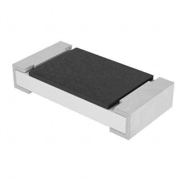
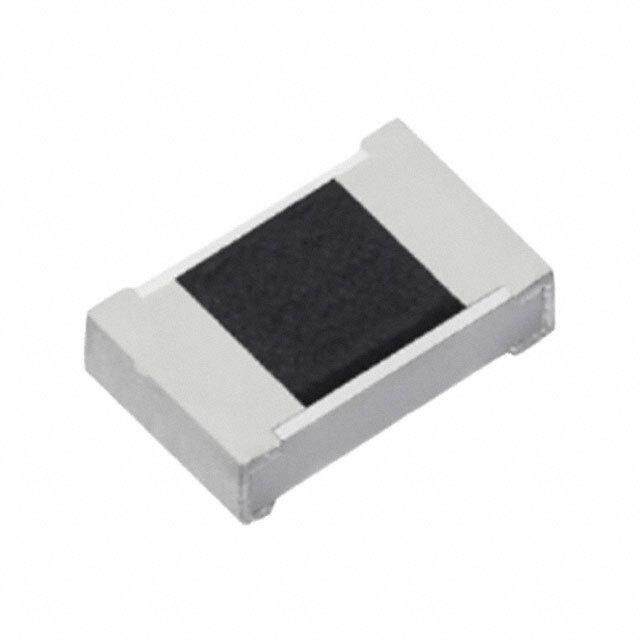
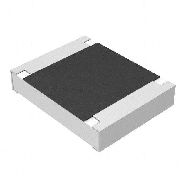
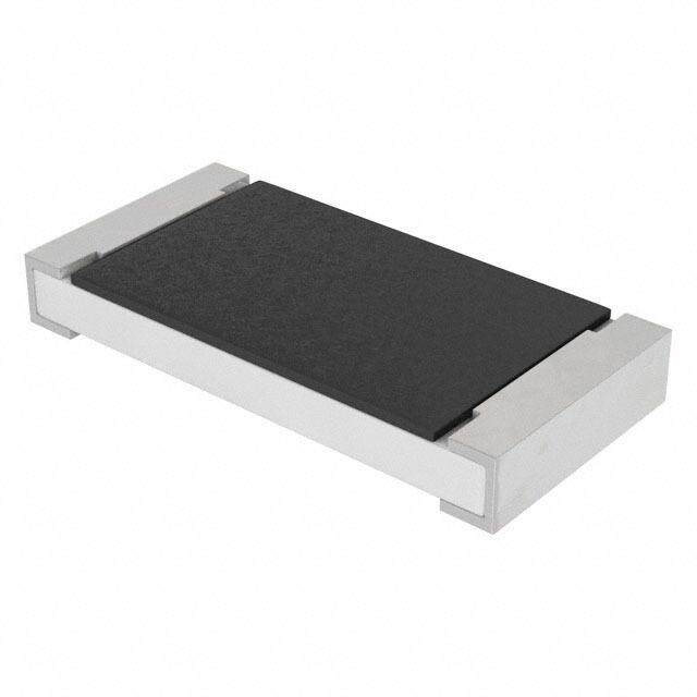
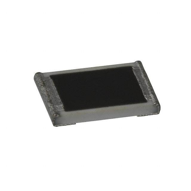
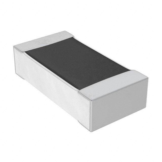
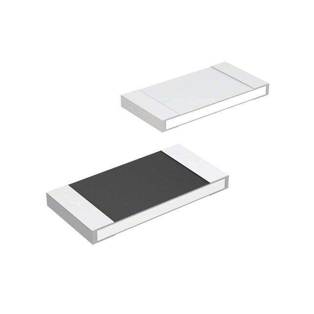
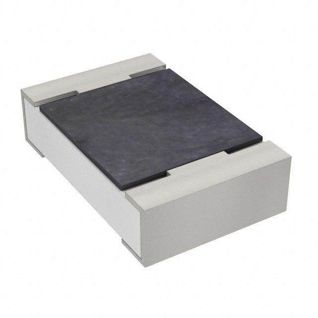
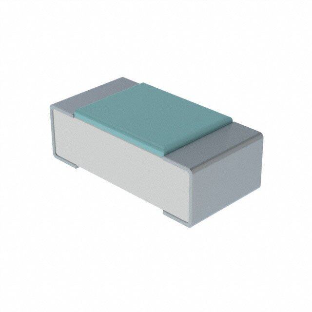
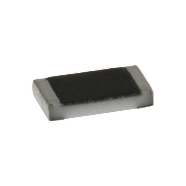
| 产品图片 |
|
| rohs | RoHS 合规性豁免无铅 / 不受限制有害物质指令(RoHS)规范要求限制 |
| 产品系列 | 薄膜电阻器,厚膜电阻器 - SMD,Bourns CR0402-J/-000GLFCR0402 |
| 数据手册 | |
| 产品型号 | CR0402-J/-000GLF |
| 产品 | Thick Film Resistors Zero-Ohm |
| 产品种类 | 厚膜电阻器 - SMD |
| 供应商器件封装 | 0402 |
| 其它名称 | CR0402-J/-000GLFCT |
| 功率(W) | 0.063W,1/16W |
| 功率额定值 | - |
| 包装 | 剪切带 (CT) |
| 商标 | Bourns |
| 外壳代码-in | 0402 |
| 外壳代码-mm | 1005 |
| 外壳宽度 | 0.5 mm |
| 外壳长度 | 1 mm |
| 外壳高度 | 0.35 mm |
| 大小/尺寸 | 0.039" 长 x 0.020" 宽(1.00mm x 0.50mm) |
| 容差 | - |
| 封装 | Reel |
| 封装/外壳 | 0402(1005 公制) |
| 封装/箱体 | 0402 (1005 metric) |
| 工作温度范围 | - 55 C to + 125 C |
| 工厂包装数量 | 10000 |
| 成分 | 厚膜 |
| 标准包装 | 1 |
| 温度系数 | - |
| 特性 | - |
| 电压额定值 | - |
| 电阻 | 0 Ohms |
| 电阻(Ω) | 0.0 |
| 端子数 | 2 |
| 类型 | Chip Resistors |
| 系列 | CR0402 |
| 高度 | 0.016"(0.40mm) |

.jpg)


- 商务部:美国ITC正式对集成电路等产品启动337调查
- 曝三星4nm工艺存在良率问题 高通将骁龙8 Gen1或转产台积电
- 太阳诱电将投资9.5亿元在常州建新厂生产MLCC 预计2023年完工
- 英特尔发布欧洲新工厂建设计划 深化IDM 2.0 战略
- 台积电先进制程称霸业界 有大客户加持明年业绩稳了
- 达到5530亿美元!SIA预计今年全球半导体销售额将创下新高
- 英特尔拟将自动驾驶子公司Mobileye上市 估值或超500亿美元
- 三星加码芯片和SET,合并消费电子和移动部门,撤换高东真等 CEO
- 三星电子宣布重大人事变动 还合并消费电子和移动部门
- 海关总署:前11个月进口集成电路产品价值2.52万亿元 增长14.8%

PDF Datasheet 数据手册内容提取
NT *RoHS VCEOARVMSIAPILOLINAASB LE Features NT MPLIA n Small package dimensions n Suitable for most types of soldering HS CO n RoHS compliant* processes *Ro n Power rating at 70 °C = 1/16 W n Standard packaging on paper tape and reel n Tight dimensional tolerances n Three layer termination process with nickel barrier prevents leaching and REE provides excellent solderability D F LEA CR0402 - Chip Resistor Electrical Characteristics Derating Curve PO DMMoepaa .wre.xxa.iire.mmta.er.t. uudi.Rn.mm .agt.o. t .WOTi .n0.e.vg o.mL.e r.@o.krp.lai.oen. d.a7rg.a .d0 a.Vt. ut.V° o..Cr..ole..t-. la ..5tR..ag..5..gae.. ..°en ...C... g........ e....t....o........ ...++...1..11..1/.551.5055600 °° WCCVVLVEREAoRDH SISF ORCNEOSE MAPRLIE ANT* er (%) 10800 w 60 Resistance Range o 1 %, E-96 d P 40 and E-24 ......10 ohms to 10 megohms e at 5 %, E-24 ........1 ohm to 20 megohms R 20 Zero Ohm Jumper ............<0.05 ohms Temperature Coefficient 0 1 % ........10 Ω ≤ R ≤ 1 MΩ ±100 ppm/℃ -55 0 70 155 1 MΩ < R ≤ 10 MΩ ±200 ppm/℃ Ambient Temperature (°C) 5 % ......10 Ω ≤ R ≤ 10 MΩ ±200 ppm/℃ 10 MΩ < R ≤ 20 MΩ ±400 ppm/℃ Standard Values Part Marking System 1 Ω ≤ R < 10 Ω -200 to +500 ppm/°C AEC-Q200 .....................Contact Bourns For Standard Values Used in Capac- No Marking on the CR0402 Chip to confirm availability itors, Inductors, and Resistors, click Resistors. here. Dimensional Drawings 0.20 ± 0.10 0.20 ± 0.10 Resistor (Ru02) Overcoat (0.008 ± 0.004) (0.008 ± 0.004) (Jumper chip is a conductor) 0.35 ± 0.05 (0.014 ± 0.002) 0.50 ± 0.05 0.25 ± 0.10 0.25 ± 0.10 (0.020 ± 0.002) (0.010 ± 0.004) (0.010 ± 0.004) 1.00 ± 0.10 Alumina Substrate (0.040 ± 0.004) Internal Electrode (Ag) Secondary Electrode (Nickel Plated) MM D IMENSIONS: (INCHES) External Electrode (tin-plated) Performance Characteristics Test Limits DR Test Procedure Method 1 % 5 % -55 ℃ for 30 minutes, +155 ℃ for 30 minutes, Thermal Shock IEC60115-1-4.19 ≤±(0.5 % + 0.05 Ω) ≤±(1 % + 0.05 Ω) 5 cycles Short Time Overload 2.5 X rated voltage for 5 seconds IEC60115-1-4.13 ≤±(2 % + 0.1 Ω) Resistance to Solder Heat 270 ±5 ℃ for 10 ±1 seconds IEC60115-1-4.18 ≤±(0.5 % + 0.05 Ω) ≤±(1 % + 0.05 Ω) Resistance to Dry Heat 125 ±5 ℃ for 96 ±4 hours IEC60115-1-4.23.2 ≤±(1 % + 0.05 Ω) ≤±(2 % + 0.1 Ω) Rated voltage for 1000 hours, 70 ℃, Load Life IEC60115-1-4.25.1 ≤±(3 % + 0.1 Ω) 1.5 hours “ON“, 0.5 hours “OFF” Rated voltage for 1000 hours, 40 ±2 ℃, Load Life with Humidity IEC60115-1-4.24 ≤±(3 % + 0.1 Ω) 90~95 % RH, 1.5 hours “ON“, 0.5 hours “OFF” Solderability 245 ±5 ℃, 2 ±0.5 seconds IEC60115-1-4.17 ≥95 % of area covered Bending 3 mm IEC60115-1-4.33 ≤±(0.5 % + 0.05 Ω) ≤±(1 % + 0.05 Ω) Dielectric Withstanding -- IEC60115-1-4.7 >100 V Voltage Insulation Resistance 100 V IEC60115-1-4.6 ≥1 GΩ *RoHS Directive 2002/95/EC Jan. 27, 2003 including annex and RoHS Recast 2011/65/EU June 8, 2011. Specifications are subject to change without notice. The device characteristics and parameters in this data sheet can and do vary in different applications and actual device performance may vary over time. Users should verify actual device performance in their specific applications.
CR0402 - Chip Resistor Soldering Profile for RoHS Compliant Chip Resistors and Arrays 275 <1>Maximum of 20 seconds between 260 °C peak +255 °C and +260 °C < 1 > 255 °C 225 220 °C e (°C)175 190 °C s6e0c o- n9d0s ur 150 °C Ramp Down erat 6 °C/second p m Te125 60 - 120 seconds 10 seconds minimum 75 Ramp Up 3 °C/second maximum 25 0 50 100 150 200 250 300 Time (seconds) Packaging Dimensions (Conforms to EIA RS-481A) 1.0 ± 0.2 1.5 + 0.1/-0 DIA. (.040 ± .020) (0.059 + 0.004/-0) 0.45 ± 0.1 (0.018 ± 0.004) 4.0 ± 0.1 1.75 ± 0.1 (0.157 ± 0.004) (0.069 ± 0.004) 2.0 (.080) 13.0 ± 0.5 0.65 ± 0.1 (0.026 ± 0.004) 3.5 ± 0.05 (.512 ± .020) (0.138 ± 0.002) 80.0 ± 1.0 1.15 ± 0.1 8.0 ± 0.2 (3.150 ± .040) (0.045 ± 0.004) (0.315 ± 0.008) 2.0 ± 0.1 Paper 20.5 (0.079 ± 0.004) (Punched) (.807) 178.0 ± 2.0 Direction of Feeding (7.008 ± .080) MM DIMENSIONS: (INCHES) 10.0 ± 1.5 (.394 ± .059) Specifications are subject to change without notice. The device characteristics and parameters in this data sheet can and do vary in different applications and actual device performance may vary over time. Users should verify actual device performance in their specific applications.
CR0402 - Chip Resistor How to Order CR 0402 - F X - 8252 G LF Model (CR = Chip Resistor) Size • 0402 Resistance Tolerance F = ±1 % ..............Used with “X” TCR code only for values from 10 ohms through 1 megohm; and Used with “W” TCR code only for values above 1 megohm. through 10 megohms. J = ±5 % ...............Used with “W” TCR code for values from 10 ohms through 10 megohms; Used with “Z” TCR code for values above 10 megohms through 20 megohms; Used with “/” TCR code for zero ohm (jumper); and for values from 1 ohm through 9.1 ohms. TCR (ppm/°C) X = ±100 W = ±200 Z = ±400 / = -200 to +500 Resistance Value For 1 % Tolerance: <100 ohms ...........“R” designates decimal point (example: 24R3 = 24.3 ohms) ≥100 ohms ............First three digits are significant, fourth digit represents number of zeros to follow (example: 8252 = 82.5k ohms). For 5 % Tolerance: <10 ohms .............“R” designates decimal point (example: 4R7 = 4.7 ohms) ≥10 ohms ..............First two digits are significant, third digit represents number of zeros to follow (example: 474 = 470k ohms; 000 = Jumper). Packaging G = Paper Tape (10,000 pcs.) on 7 ” Plastic Reel Termination LF = Tin-plated (RoHS compliant) REV. 11/16 Specifications are subject to change without notice. The device characteristics and parameters in this data sheet can and do vary in different applications and actual device performance may vary over time. Users should verify actual device performance in their specific applications.