
 Datasheet下载
- 型号: CPC1907B
- 制造商: IXYS
- 库位|库存: xxxx|xxxx
- 要求:
| 数量阶梯 | 香港交货 | 国内含税 |
| +xxxx | $xxxx | ¥xxxx |
查看当月历史价格
查看今年历史价格
CPC1907B产品简介:
ICGOO电子元器件商城为您提供CPC1907B由IXYS设计生产,在icgoo商城现货销售,并且可以通过原厂、代理商等渠道进行代购。 CPC1907B价格参考。IXYSCPC1907B封装/规格:固态继电器, 固体继电器 继电器 SPST-NO(1 Form A) 8-SOP (0.400",10.16mm 宽)。您可以下载CPC1907B参考资料、Datasheet数据手册功能说明书,资料中有CPC1907B 详细功能的应用电路图电压和使用方法及教程。
IXYS Integrated Circuits Division生产的固态继电器型号CPC1907B是一种高性能的光电耦合固态继电器,适用于多种工业和商业应用场景。以下是其主要的应用领域及特点:

 1. 工业自动化控制
   - 应用:CPC1907B广泛用于工业自动化设备中,如PLC(可编程逻辑控制器)、机器人控制系统、电机驱动器等。
   - 优势:它能够实现高电压负载的开关控制,同时提供良好的电气隔离性能,确保控制电路的安全性和稳定性。

 2. 家用电器
   - 应用:在家电产品中,如洗衣机、空调、冰箱等,用于控制压缩机、风扇电机或其他大功率组件的启停。
   - 优势:无机械触点设计,避免了传统继电器因触点磨损导致的故障问题,延长了使用寿命。

 3. 照明系统
   - 应用:用于LED灯具、舞台灯光、广告牌照明等场景中的电源切换。
   - 优势:支持快速开关操作,适合需要频繁切换的照明环境,同时减少电磁干扰(EMI)。

 4. 医疗设备
   - 应用:在医疗仪器中,如监护仪、超声波设备等,用于控制电源或信号传输。
   - 优势:具有高可靠性、低漏电流特性,满足医疗设备对安全性和精度的严格要求。

 5. 通信设备
   - 应用:在通信基站、网络设备中,用于电源管理或信号隔离。
   - 优势:能够在恶劣环境下稳定工作,具备较强的抗干扰能力。

 6. 汽车电子
   - 应用:应用于车载电子系统中,如车灯控制、电动座椅调节、发动机管理等。
   - 优势:耐高温、抗震性强,适应汽车运行中的复杂工况。

 7. 测试与测量设备
   - 应用:用于数据采集系统、示波器等测试设备中,实现信号的隔离与切换。
   - 优势:提供精确的开关控制,确保测试结果的准确性。

 总结
CPC1907B凭借其高绝缘耐压(3750Vrms)、低导通电阻(典型值为0.8Ω)以及宽工作温度范围(-40°C至+85°C),成为许多需要高可靠性和长寿命应用的理想选择。无论是工业级还是消费级市场,该型号都能提供卓越的性能表现。
| 参数 | 数值 |
| 产品目录 | |
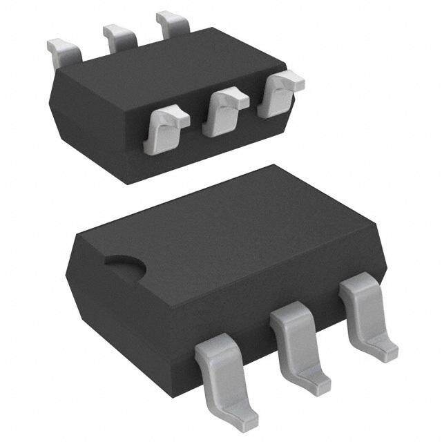
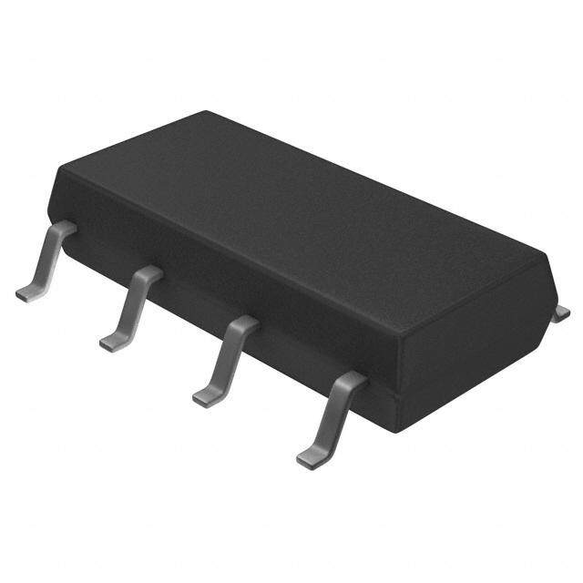
| 描述 | RELAY OPTOMOS SP-NO 6A 8-SOP固态继电器-PCB安装 8Pin Single Pole NOR Mally Open SS Relay |
| 产品分类 | |
| 品牌 | IXYS Integrated Circuits DivisionIXYS Integrated Circuits |
| 产品手册 | |
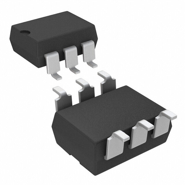
| 产品图片 |
|
| rohs | 符合RoHS无铅 / 符合限制有害物质指令(RoHS)规范要求 |
| 产品系列 | 固态继电器,固态继电器-PCB安装,IXYS Integrated Circuits CPC1907BCPC, OptoMOS® |
| mouser_ship_limit | 该产品可能需要其他文件才能进口到中国。 |
| 数据手册 | |
| 产品型号 | CPC1907BCPC1907B |
| 产品 | Automation Relays |
| 产品种类 | 固态继电器-PCB安装 |
| 产品类型 | PCB Mount |
| 供应商器件封装 | 8-SOIC |
| 其它名称 | CLA394 |
| 包装 | 管件 |
| 商标 | IXYS Integrated Circuits |
| 安装类型 | 表面贴装 |
| 安装风格 | Through Hole |
| 导通电阻 | 60 毫欧 |
| 导通电阻—最大值 | 0.06 Ohms |
| 封装 | Tube |
| 封装/外壳 | 8-SOP (0.400", 10.16mm) |
| 封装/箱体 | ISOPLUS-264 |
| 工厂包装数量 | 25 |
| 最大工作温度 | + 85 C |
| 最小工作温度 | - 40 C |
| 标准包装 | 25 |
| 电压-负载 | 0 ~ 60 V |
| 电压-输入 | 1.2VDC |
| 电路 | SPST-NO(1 Form A) |
| 端子类型 | 鸥翼型 |
| 端接类型 | Solder Pin |
| 系列 | CPC1907 |
| 继电器类型 | |
| 触点形式 | SPST (1 Form A) |
| 负载电流 | 6A |
| 负载电流额定值 | 6 A |
| 输入转输出绝缘方法 | Optocoupler |
| 输出类型 | AC,DC |
| 输出设备 | MOSFET |


- 商务部:美国ITC正式对集成电路等产品启动337调查
- 曝三星4nm工艺存在良率问题 高通将骁龙8 Gen1或转产台积电
- 太阳诱电将投资9.5亿元在常州建新厂生产MLCC 预计2023年完工
- 英特尔发布欧洲新工厂建设计划 深化IDM 2.0 战略
- 台积电先进制程称霸业界 有大客户加持明年业绩稳了
- 达到5530亿美元!SIA预计今年全球半导体销售额将创下新高
- 英特尔拟将自动驾驶子公司Mobileye上市 估值或超500亿美元
- 三星加码芯片和SET,合并消费电子和移动部门,撤换高东真等 CEO
- 三星电子宣布重大人事变动 还合并消费电子和移动部门
- 海关总署:前11个月进口集成电路产品价值2.52万亿元 增长14.8%
.jpg)
PDF Datasheet 数据手册内容提取
CPC1907B Single-Pole, Normally Open Power SOIC OptoMOS® Relay I C D NTEGRATED IRCUITS IVISION Parameter Rating Units Description Blocking Voltage 60 V The CPC1907B is a single-pole, normally open P Load Current ±6 A (1-Form-A) solid state relay that employs optically DC On-Resistance 0.06 coupled MOSFET technology to provide 5000V of rms input to output isolation. Features Switching of the efficient MOSFET switches is controlled by the photovoltaic die using the patented (cid:129) Handle Load Currents Up to ±6A or 6A DC rms OptoMOS architecture while activation of the output (cid:129) 5000V Input/Output Isolation rms is controlled by a highly efficient GaAlAs infrared (cid:129) Power SOIC Package LED. The combination of low on-resistance and high (cid:129) 12.5mm External Creepage Distance load current handling capabilities makes the relay with Appropriate Layout suitable for a variety of high-performance switching (cid:129) High Reliability applications. (cid:129) No Moving Parts (cid:129) Low Drive Power Requirements (TTL/CMOS Compatible) (cid:129) Arc-Free With No Snubbing Circuits Approvals (cid:129) No EMI/RFI Generation (cid:129) UL 508 Certified Component: File E69938 (cid:129) CSA Industrial Control Switches Approval: Pending Applications Ordering Information (cid:129) Industrial Controls (cid:129) Security: Door Latches, Solenoids, Annunciators Part # Description (cid:129) Motor Control CPC1907B 8-Pin Power SOIC Package (25 per tube) (cid:129) Heating, Ventilation, and Air Conditioning Control (HVAC) (cid:129) Robotics Pin Configuration (cid:129) Starter Ignition Circuits 8 7 6 5 (cid:129) Medical Equipment—Patient/Equipment Isolation (cid:129) Instrumentation (cid:129) Multiplexers (cid:129) Electronic Switching (cid:129) I/O Subsystems (cid:129) Home Appliances (cid:129) DC Power Supplies 1 2 3 4 (cid:129) Aerospace N/C + LED – LED N/C Switching Characteristics of Normally Open Devices Form-A I F 90% I 10% LOAD t t e on off Pb 3 DS-CPC1907B-R02 www.ixysic.com 1
I C D CPC1907B NTEGRATED IRCUITS IVISION Absolute Maximum Ratings @ 25ºC (Unless Otherwise Noted) Parameter Ratings Units Absolute Maximum Ratings are stress ratings. Stresses in Blocking Voltage 60 V excess of these ratings can cause permanent damage to the device. Functional operation of the device at conditions beyond Reverse Input Voltage 5 V those indicated in the operational sections of this data sheet is Input control Current 50 mA not implied. Peak (10ms) 1 A Input Power Dissipation 1 150 mW Total Power Dissipation 2 2400 mW Isolation Voltage, Input to Output 5000 V (60 Seconds Maximum) rms ESD, Human Body Model 8 kV Operational Temperature -40 to +85 °C Storage Temperature -40 to +125 °C 1 Derate linearly 3.33mW / ºC 2 Derate linearly 20mW / ºC Electrical Characteristics @ 25ºC (Unless Otherwise Noted) Parameter Conditions Symbol Min Typ Max Units Output Characteristics Load Current, Continuous free air I - - 6 ±A , A L DC rms Peak Load Current t = 10ms I - - 20 ±A LPK P On-Resistance1 I=1A R - - 0.06 L ON Off-State Leakage Current V=60V I - - 1 µA L P LEAK Switching Speeds Turn-On t - 2.7 5 I =5mA, I=100mA on ms Turn-Off F L t - 0.14 1 off Output Capacitance V=50V, f=1MHz C - 340 - pF L OUT Input Characteristics LED Current to Activate 2 I=1A I - 1.5 5 mA L F LED Current to Deactivate - I 0.6 - - mA F Input Voltage Drop I =5mA V 0.9 1.2 1.4 V F F Reverse Input Current V =5V I - - 10 µA R R Input/Output Characteristics Capacitance, Input/Output f=1MHz I - 2 - pF I/O 1 Measurement taken within 1 second of on-time. 2 For high temperature operation (T>60ºC), a LED current of 10mA is recommended. A 2 www.ixysic.com R02
I C D CPC1907B NTEGRATED IRCUITS IVISION PERFORMANCE DATA @25ºC (Unless Otherwise Noted)* Typical LED Forward Voltage Drop Typical Turn-On Time Typical Turn-Off Time (N=50, I=5mA) (N=50, I=5mA, I=100mA) (N=50, I=5mA, I=100mA) 30 F 25 F L 20 F L 25 20 N) N) N)15 nt ( 20 nt (15 nt ( u u u Co 15 Co Co10 Device 150 Device 150 Device 5 0 0 0 1.235 1.240 1.245 1.250 1.255 1.260 1.265 2.10 2.40 2.70 3.00 3.30 3.60 3.90 0.105 0.115 0.125 0.135 0.145 0.155 0.165 LED Forward Voltage (V) Turn-On Time (ms) Turn-Off Time (ms) Typical I for Switch Operation Typical On-Resistance Distribution Typical Blocking Voltage Distribution F (N=50, I=100mA) (N=50, I=5mA, I=1A) (N=50, I=0mA) 25 L 20 F L 25 F 20 20 N) N) 15 N) unt ( 15 unt ( unt (15 Co Co 10 Co Device 150 Device 5 Device 105 0 0 0 1.30 1.45 1.60 1.75 1.90 2.05 2.20 54.5 55.0 55.5 56.0 56.5 57.0 57.5 81.75 82.50 83.25 84.00 84.75 85.50 LED Forward Current (mA) On-Resistance (m(cid:58)) Blocking Voltage (VP) Typical Turn-On Time Typical Turn-Off Time Typical LED Forward Voltage Drop vs. LED Forward Current vs. LED Forward Current vs. Temperature (I=100mA) (I=100mA) 1.6 7 L 150 L I=50mA V) IF=20mA 6 Voltage (11..45 IIFFF==51m0mAA me (ms) 45 me (s)(cid:80)145 ward 1.3 On Ti 3 Off Ti140 D For1.2 Turn- 2 Turn-135 E 1 L 1.1 0 130 -40 -20 0 20 40 60 80 100 0 10 20 30 40 50 0 10 20 30 40 50 Temperature (ºC) LED Forward Current (mA) LED Forward Current (mA) Typical Turn-On Time Typical Turn-Off Time Typical I for Switch Operation vs. Temperature vs. Temperature F (I=1A) (I=100mA) (I=100mA) 2.2 L 3.5 L 170 L I=5mA nt (mA)12..80 me (ms)23..50 F me (s)(cid:80)115600 LED Curre11..46 Turn-On Ti12..50 IF=10mA Turn-Off Ti111234000 IF=5mA IF=10mA 1.2 1.0 110 -40 -20 0 20 40 60 80 100 -40 -20 0 20 40 60 80 100 -40 -20 0 20 40 60 80 100 Temperature (ºC) Temperature (ºC) Temperature (ºC) *The Performance data shown in the graphs above is typical of device performance. For guaranteed parameters not indicated in the written specifi cations, please contact our application department. R02 www.ixysic.com 3
I C D CPC1907B NTEGRATED IRCUITS IVISION PERFORMANCE DATA @25ºC (Unless Otherwise Noted)* Typical On-Resistance Maximum Load Current vs. Temperature Typical Load Current vs. Load Voltage vs. Temperature (I=5mA, I=1A) (I=5mA) (I=5mA) 70 F L 6 F 7 F 65 4 6 n-Resistance (m)(cid:58)45565050 Load Current (A) -202 Load Current (A) 2345 O40 -4 1 35 -6 0 -40 -20 0 20 40 60 80 100 -0.3 -0.2 -0.1 0.0 0.1 0.2 0.3 -40 -20 0 20 40 60 80 100 Temperature (ºC) Load Voltage (V) Temperature (ºC) Leakage Current vs. Temperature Typical Blocking Voltage Across Pins 5&6, 7&8 Output Capacitance vs. Load Voltage vs. Temperature (V=60V) (I=0mA, f=1MHz) L F 90 1.0 1000 Blocking Voltage (V)P 8888802468 Leakage Current (A)(cid:80)0000....2468 Output Capacitance (pF)456789000000000000 78 0 300 -40 -20 0 20 40 60 80 100 -40 -20 0 20 40 60 80 100 0 10 20 30 40 50 Temperature (ºC) Temperature (ºC) Load Voltage (V) Energy Rating Curve 35 30 A) nt ( 25 e urr 20 C ad 15 o L 10 5 10(cid:80)s 100(cid:80)s 1ms 10ms100ms 1s 10s 100s Time *The Performance data shown in the graphs above is typical of device performance. For guaranteed parameters not indicated in the written specifi cations, please contact our application department. 4 www.ixysic.com R02
I C D CPC1907B NTEGRATED IRCUITS IVISION Manufacturing Information Moisture Sensitivity All plastic encapsulated semiconductor packages are susceptible to moisture ingression. IXYS Integrated Circuits Division classified all of its plastic encapsulated devices for moisture sensitivity according to the latest version of the joint industry standard, IPC/JEDEC J-STD-020, in force at the time of product evaluation. We test all of our products to the maximum conditions set forth in the standard, and guarantee proper operation of our devices when handled according to the limitations and information in that standard as well as to any limitations set forth in the information or standards referenced below. Failure to adhere to the warnings or limitations as established by the listed specifications could result in reduced product performance, reduction of operable life, and/or reduction of overall reliability. This product carries a Moisture Sensitivity Level (MSL) rating as shown below, and should be handled according to the requirements of the latest version of the joint industry standard IPC/JEDEC J-STD-033. Device Moisture Sensitivity Level (MSL) Rating CPC1907B MSL 1 ESD Sensitivity This product is ESD Sensitive, and should be handled according to the industry standard JESD-625. Reflow Profile This product has a maximum body temperature and time rating as shown below. All other guidelines of J-STD-020 must be observed. Device Maximum Temperature x Time CPC1907B 245ºC for 30 seconds Board Wash IXYS Integrated Circuits Division recommends the use of no-clean flux formulations. However, board washing to remove flux residue is acceptable. Since IXYS Integrated Circuits Division employs the use of silicone coating as an optical waveguide in many of its optically isolated products, the use of a short drying bake could be necessary if a wash is used after solder reflow processes. Chlorine- or Fluorine-based solvents or fluxes should not be used. Cleaning methods that employ ultrasonic energy should not be used. e Pb 3 R02 www.ixysic.com 5
I C D CPC1907B NTEGRATED IRCUITS IVISION MECHANICAL DIMENSIONS CPC1907B Recommended PCB Pattern 21.082 ± 0.381 (0.830 ± 0.015) 3.302 ± 0.051 (0.130 ± 0.002) Pin 8 0.127 ± 0.076 (0.005 ± 0.003) 2.00 16.764 ± 0.381 10.160 ± 0.254 15.90 (0.079) (0.660 ± 0.015) (0.400 ± 0.010) (0.626) 0.889 ± 0.127 Pin 1 (0.035 ± 0.005) 1.016 ± 0.127 0.762 ± 0.102 (0.040 ± 0.005) 0.381 ± 0.025 5.080 (0.030 ± 0.004) 1.651 ± 0.102 (0.015 ± 0.001) (0.200) 0.95 5.080 ± 0.127 1(.05.2046 0ty)p (0.065 ± 0.004) 7.622 (0.037) (0.200 ± 0.005) 5.080 ± 0.127 Dimensions (0.300) 7.620 ± 0.127 (0.200 ± 0.005) Unless Otherwise Noted (50..028000) (0.300 ± 0.005) mm Note: Pin-to-pin tolerances are non-cumulative. (inches) For additional information please visit our website at: www.ixysic.com IXYS Integrated Circuits Division makes no representations or warranties with respect to the accuracy or completeness of the contents of this publication and reserves the right to make changes to specifications and product descriptions at any time without notice. Neither circuit patent licenses nor indemnity are expressed or implied. Except as set forth in IXYS Integrated Circuits Division’s Standard Terms and Conditions of Sale, IXYS Integrated Circuits Division assumes no liability whatsoever, and disclaims any express or implied warranty, relating to its products including, but not limited to, the implied warranty of merchantability, fitness for a particular purpose, or infringement of any intellectual property right. The products described in this document are not designed, intended, authorized or warranted for use as components in systems intended for surgical implant into the body, or in other applications intended to support or sustain life, or where malfunction of IXYS Integrated Circuits Division’s product may result in direct physical harm, injury, or death to a person or severe property or environmental damage. IXYS Integrated Circuits Division reserves the right to discontinue or make changes to its products at any time without notice. Specification: DS-CPC1907B-R02 ©Copyright 2013, IXYS Integrated Circuits Division OptoMOS® is a registered trademark of IXYS Integrated Circuits Division All rights reserved. Printed in USA. 6 2/12/2013
Mouser Electronics Authorized Distributor Click to View Pricing, Inventory, Delivery & Lifecycle Information: I XYS: CPC1907B