 Datasheet下载
- 型号: CM1293A-04SO
- 制造商: ON Semiconductor
- 库位|库存: xxxx|xxxx
- 要求:
| 数量阶梯 | 香港交货 | 国内含税 |
| +xxxx | $xxxx | ¥xxxx |
查看当月历史价格
查看今年历史价格
CM1293A-04SO产品简介:
ICGOO电子元器件商城为您提供CM1293A-04SO由ON Semiconductor设计生产,在icgoo商城现货销售,并且可以通过原厂、代理商等渠道进行代购。 CM1293A-04SO价格参考¥0.24-¥0.44。ON SemiconductorCM1293A-04SO封装/规格:TVS - 二极管, 9.9V (Typ) Clamp 1A (8/20µs) Ipp Tvs Diode Surface Mount SC-74。您可以下载CM1293A-04SO参考资料、Datasheet数据手册功能说明书,资料中有CM1293A-04SO 详细功能的应用电路图电压和使用方法及教程。
ON Semiconductor(安森美)的CM1293A-04SO是一款瞬态电压抑制(TVS)二极管阵列,主要用于保护敏感电子元件免受静电放电(ESD)、浪涌电压和瞬态干扰的损害。该器件采用小型SO-8封装,集成多个TVS二极管,适用于高速数据线和接口电路的过压保护。

典型应用场景包括:

1. USB接口保护:广泛用于USB 2.0或USB OTG接口中,防止人体静电或连接过程中产生的高压损坏主控芯片。
2. 便携式电子设备:如智能手机、平板电脑、可穿戴设备等,保护其内部精密电路不受日常使用中频繁插拔或环境静电影响。
3. 通信端口防护:适用于HDMI、音频/视频接口、串行数据线等信号线路,提供低电容特性以确保信号完整性。
4. 消费类电子产品:在机顶盒、数码相机、移动电源等产品中,用于提升系统可靠性和抗干扰能力。

CM1293A-04SO具有低工作电压(约5.0V)、高ESD耐受能力(可达±15kV接触放电)、响应速度快和低漏电流等特点,能够在不影响正常信号传输的前提下提供高效保护。其设计符合IEC 61000-4-2 Level 4等国际电磁兼容标准,适合对空间和性能要求较高的应用场合。
| 参数 | 数值 |
| 产品目录 | |
| 描述 | TVS DIODE 3.3VWM 9.9VC SC74 |
| 产品分类 | |
| 品牌 | ON Semiconductor |
| 数据手册 | |
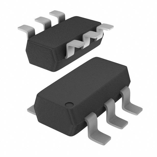
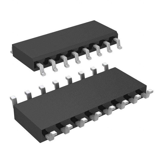
| 产品图片 |
|
| 产品型号 | CM1293A-04SO |
| rohs | 无铅 / 符合限制有害物质指令(RoHS)规范要求 |
| 产品系列 | - |
| 不同频率时的电容 | - |
| 供应商器件封装 | SC-74 |
| 其它名称 | CM1293A-04SOOSDKR |
| 功率-峰值脉冲 | - |
| 包装 | Digi-Reel® |
| 单向通道 | - |
| 双向通道 | 4 |
| 安装类型 | 表面贴装 |
| 封装/外壳 | SC-74,SOT-457 |
| 工作温度 | -40°C ~ 85°C (TA) |
| 应用 | 通用 |
| 标准包装 | 1 |
| 电压-击穿(最小值) | - |
| 电压-反向关态(典型值) | 3.3V |
| 电压-箝位(最大值)@Ipp | 9.9V (标准) |
| 电流-峰值脉冲(10/1000µs) | 1A (8/20µs) |
| 电源线路保护 | 是 |
| 类型 | 转向装置(轨至轨) |


- 商务部:美国ITC正式对集成电路等产品启动337调查
- 曝三星4nm工艺存在良率问题 高通将骁龙8 Gen1或转产台积电
- 太阳诱电将投资9.5亿元在常州建新厂生产MLCC 预计2023年完工
- 英特尔发布欧洲新工厂建设计划 深化IDM 2.0 战略
- 台积电先进制程称霸业界 有大客户加持明年业绩稳了
- 达到5530亿美元!SIA预计今年全球半导体销售额将创下新高
- 英特尔拟将自动驾驶子公司Mobileye上市 估值或超500亿美元
- 三星加码芯片和SET,合并消费电子和移动部门,撤换高东真等 CEO
- 三星电子宣布重大人事变动 还合并消费电子和移动部门
- 海关总署:前11个月进口集成电路产品价值2.52万亿元 增长14.8%


PDF Datasheet 数据手册内容提取
CM1293A-04SO 4-Channel Low Capacitance ESD Protection Array Product Description CM1293A−04SO has been designed to provide ESD protection for http://onsemi.com electronic components or subsystems requiring minimal capacitive loading. This device is ideal for protecting systems with high data and clock rates or for circuits requiring low capacitive loading. Each ESD channel consists of a pair of diodes in series that steer the positive or SC−74 negative ESD current pulse to either the positive (V ) or negative (V ) SO SUFFIX P N CASE 318F supply rail. A Zener diode is embedded between VP and VN which helps protect the V rail against ESD strikes. This device protects CC BLOCK DIAGRAM against ESD pulses up to 8 kV contact discharge) per the IEC61000−4−2 Level 4 standard. VP This device is particularly well−suited for protecting systems using CH1 CH2 CH3 CH4 high−speed ports such as USB2.0, IEEE1394 (FireWire, i.LINK(cid:2)), Serial ATA, DVI, HDMI, and corresponding ports in removable storage, digital camcorders, DVD−RW drives and other applications where extremely low loading capacitance with ESD protection are required in a small package footprint. VN CM1293A−04SO Features Four Channels of ESD Protection MARKING DIAGRAM Provides ESD Protection to IEC61000−4−2 8 kV Contact Discharge Low Loading Capacitance of 2.0 pF Max XXXM(cid:3) (cid:3) Low Clamping Voltage 1 Channel I/O to I/O Capacitance 1.5 pF Typical Zener Diode Protects Supply Rail and Eliminates the Need for External By−Pass Capacitors XXX = Specific Device Code M = Date Code Each I/O Pin Can Withstand over 1000 ESD Strikes* (cid:3) = Pb−Free Package This Device is Pb−Free and is RoHS Compliant** (Note: Microdot may be in either location) Applications ORDERING INFORMATION DVI Ports, HDMI Ports in Notebooks, Set Top Boxes, Digital TVs, LCD Displays Device Package Shipping† Serial ATA Ports in Desktop PCs and Hard Disk Drives CM1293A−04SO SC−74 3,000 / (Pb−Free) Tape & Reel PCI Express Ports General Purpose High−Speed Data Line ESD Protection †For information on tape and reel specifications, including part orientation and tape sizes, please refer to our Tape and Reel Packaging Specification Brochure, BRD8011/D. **Standard test condition is IEC61000−4−2 level 4 test circuit with each pin subjected to 8 kV contact discharge for 1000 pulses. Discharges are timed at 1 second intervals and all 1000 strikes are completed in one continuous test run. The part is then subjected to standard production test to verify that all of the tested parameters are within spec after the 1000 strikes. **For additional information on our Pb−Free strategy and soldering details, please download the ON Semiconductor Soldering and Mounting Techniques Reference Manual, SOLDERRM/D. Semiconductor Components Industries, LLC, 2012 1 Publication Order Number: January, 2012 − Rev. 0 CM1293A−04SO/D
CM1293A−04SO PACKAGE/PINOUT DIAGRAM Table 1. PIN DESCRIPTIONS Pin Name Type Description Top View 1 CH1 I/O ESD Channel CH1 CH4 2 VN GND Negative Voltage Supply Rail VN 63 VP 3 CH2 I/O ESD Channel 5 CH2 CH3 4 CH3 I/O ESD Channel 4−Channel SC−74 5 VP PWR Positive Voltage Supply Rail 6 CH4 I/O ESD Channel SPECIFICATIONS Table 2. ABSOLUTE MAXIMUM RATINGS Parameter Rating Units Operating Supply Voltage (VP − VN) 6.0 V Operating Temperature Range –40 to +85 C Storage Temperature Range –65 to +150 C DC Voltage at any Channel Input (VN − 0.5) to (VP + 0.5) V Stresses exceeding Maximum Ratings may damage the device. Maximum Ratings are stress ratings only. Functional operation above the Recommended Operating Conditions is not implied. Extended exposure to stresses above the Recommended Operating Conditions may affect device reliability. Table 3. STANDARD OPERATING CONDITIONS Parameter Rating Units Operating Temperature Range –40 to +85 C Package Power Rating 225 mW Table 4. ELECTRICAL OPERATING CHARACTERISTICS (Note 1) Symbol Parameter Conditions Min Typ Max Units VP Operating Supply Voltage (VP−VN) 3.3 5.5 V IP Operating Supply Current (VP−VN) = 3.3 V 8.0 (cid:2)A VF Diode Forward Voltage IF = 8 mA, TA = 25C 0.90 V ILEAK Channel Leakage Current TA = 25C, VP = 5 V, VN = 0 V 0.1 1.0 (cid:2)A CIN Channel Input Capacitance At 1 MHz, VP = 3.3 V, VN = 0 V, VIN = 1.65 V 2.0 pF (cid:3)CIO Channel I/O to I/O Capacitance 1.5 pF VESD ESD Protection kV Peak Discharge Voltage at any Channel Input, in System Contact Discharge per TA = 25C (Notes 2 and 3) 8 IEC 61000−4−2 Standard VCL Channel Clamp Voltage TA = 25C, IPP = 1A, tP = 8/20 (cid:2)S V Positive Transients (Note 3) +9.9 Negative Transients –1.6 RDYN Dynamic Resistance TA = 25C, IPP = 1A, tP = 8/20 (cid:2)S (cid:4) Positive Transients (Note 3) 0.96 Negative Transients 0.5 1. All parameters specified at TA = –40C to +85C unless otherwise noted. 2. Standard IEC 61000−4−2 with CDischarge = 150 pF, RDischarge = 330 (cid:4), VP = 3.3 V, VN grounded. 3. These measurements performed with no external capacitor on VP. http://onsemi.com 2
CM1293A−04SO PERFORMANCE INFORMATION Input Channel Capacitance Performance Curves Figure 1. Typical Variation of C vs. V IN IN (f = 1 MHz, V = 3.3 V, V = 0 V, 0.1 (cid:2)F Chip Capacitor between V and V , 25(cid:2)C) P N P N Figure 2. Typical Variation of C vs. Temp IN (f = 1 MHz, V = 30 mV, V = 3.3 V, V = 0 V, 0.1 (cid:2)F Chip Capacitor between V and V ) IN P N P N http://onsemi.com 3
CM1293A−04SO PERFORMANCE INFORMATION (Cont’d) Typical Filter Performance (nominal conditions unless specified otherwise, 50 (cid:3) Environment) Figure 3. Insertion Loss (S21) vs. Frequency (0 V DC Bias, VP = 3.3 V) Figure 4. Insertion Loss (S21) vs. Frequency (2.5 V DC Bias, VP = 3.3 V) http://onsemi.com 4
CM1293A−04SO APPLICATION INFORMATION Design Considerations In order to realize the maximum protection against ESD pulses, care must be taken in the PCB layout to minimize parasitic series inductances on the Supply/Ground rails as well as the signal trace segment between the signal input (typically a connector) and the ESD protection device. Refer to Figure 5, which illustrates an example of apositive ESD pulse striking an input channel. The parasitic series inductance back to the power supply is represented by L1 and L2. The voltage VCL on the line being protected is: VCL = Fwd voltage drop of D1 + VSUPPLY + L1 x d(IESD) / dt+ L2 x d(IESD) / dt where I is the ESD current pulse, and V is the positive supply voltage. ESD SUPPLY An ESD current pulse can rise from zero to its peak value in a very short time. As an example, a level 4 contact discharge per the IEC61000−4−2 standard results in a current pulse that rises from zero to 30 Amps in 1 ns. Here d(I )/dt can be ESD approximated by (cid:3)IESD/(cid:3)t, or 30/(1x10−9). So just 10 nH of series inductance (L1 and L2 combined) will lead to a 300V increment in V ! CL Similarly for negative ESD pulses, parasitic series inductance from the V pin to the ground rail will lead to drastically N increased negative voltage on the line being protected. The CM1293 has an integrated Zener diode between V and V . This greatly reduces the effect of supply rail inductance P N L on V by clamping V at the breakdown voltage of the Zener diode. However, for the lowest possible V , especially when 2 CL P CL VP is biased at a voltage significantly below the Zener breakdown voltage, it is recommended that a 0.22 F ceramic chip capacitor be connected between V and the ground plane. P As a general rule, the ESD Protection Array should be located as close as possible to the point of entry of expected electrostatic discharges. The power supply bypass capacitor mentioned above should be as close to the V pin of the Protection P Array as possible, with minimum PCB trace lengths to the power supply, ground planes and between the signal input and the ESD device to minimize stray series inductance. L2 POSITIVE SUPPLY RAIL VCC VP PATH OF ESD CURRENT PULSE IESO ÇÇÇÇÇÇ ÇÇÇÇÇÇ ÇÇÇÇÇÇ LINE BEING ÇÇDÇ1 ÇÇÇ L1 PROTECTED ÇÇSYÇSTEMÇ ORÇÇ 0.22 (cid:2)F ÇÇÇÇÇÇ ÇÇCIRÇCUITÇRYÇÇ BEING ONE CHANNEL ÇÇÇCHÇANNÇEL Ç INPUT ÇÇPRÇOTEÇCTEÇD Ç D2 25 A VCL ÇÇÇÇÇÇ ÇÇÇÇÇÇ 0 A GROUND RAIL VN CHASSIS GROUND Figure 5. Application of Positive ESD Pulse between Input Channel and Ground http://onsemi.com 5
CM1293A−04SO PACKAGE DIMENSIONS SC−74 CASE 318F−05 ISSUE M NOTES: D 1. DIMENSIONING AND TOLERANCING PER ANSI Y14.5M, 1982. 2. CONTROLLING DIMENSION: INCH. 3. MAXIMUM LEAD THICKNESS INCLUDES LEAD FINISH THICKNESS. MINIMUM LEAD 6 5 4 THICKNESS IS THE MINIMUM THICKNESS HE E 4. 3O1F8 FB−A0S1E, −M0A2T, E−R03IA, −L.04 OBSOLETE. NEW 1 2 3 STANDARD 318F−05. MILLIMETERS INCHES b DIM MIN NOM MAX MIN NOM MAX A 0.90 1.00 1.10 0.035 0.039 0.043 e A1 0.01 0.06 0.10 0.001 0.002 0.004 b 0.25 0.37 0.50 0.010 0.015 0.020 c 0.10 0.18 0.26 0.004 0.007 0.010 (cid:4) D 2.90 3.00 3.10 0.114 0.118 0.122 C E 1.30 1.50 1.70 0.051 0.059 0.067 0.05 (0.002) A e 0.85 0.95 1.05 0.034 0.037 0.041 L 0.20 0.40 0.60 0.008 0.016 0.024 L HE 2.50 2.75 3.00 0.099 0.108 0.118 A1 (cid:4) 0 − 10 0 − 10 SOLDERING FOOTPRINT* 2.4 0.094 0.95 1.9 0.037 0.074 0.95 0.7 0.037 0.028 1.0 0.039 (cid:2) mm (cid:3) SCALE 10:1 inches *For additional information on our Pb−Free strategy and soldering details, please download the ON Semiconductor Soldering and Mounting Techniques Reference Manual, SOLDERRM/D. FireWire is a registered trademark of Apple Computer, Inc. i.LINK is a trademark of Sony Corporation. ON Semiconductor and are registered trademarks of Semiconductor Components Industries, LLC (SCILLC). SCILLC reserves the right to make changes without further notice to any products herein. SCILLC makes no warranty, representation or guarantee regarding the suitability of its products for any particular purpose, nor does SCILLC assume any liability arising out of the application or use of any product or circuit, and specifically disclaims any and all liability, including without limitation special, consequential or incidental damages. “Typical” parameters which may be provided in SCILLC data sheets and/or specifications can and do vary in different applications and actual performance may vary over time. All operating parameters, including “Typicals” must be validated for each customer application by customer’s technical experts. SCILLC does not convey any license under its patent rights nor the rights of others. SCILLC products are not designed, intended, or authorized for use as components in systems intended for surgical implant into the body, or other applications intended to support or sustain life, or for any other application in which the failure of the SCILLC product could create a situation where personal injury or death may occur. Should Buyer purchase or use SCILLC products for any such unintended or unauthorized application, Buyer shall indemnify and hold SCILLC and its officers, employees, subsidiaries, affiliates, and distributors harmless against all claims, costs, damages, and expenses, and reasonable attorney fees arising out of, directly or indirectly, any claim of personal injury or death associated with such unintended or unauthorized use, even if such claim alleges that SCILLC was negligent regarding the design or manufacture of the part. SCILLC is an Equal Opportunity/Affirmative Action Employer. This literature is subject to all applicable copyright laws and is not for resale in any manner. PUBLICATION ORDERING INFORMATION LITERATURE FULFILLMENT: N. American Technical Support: 800−282−9855 Toll Free ON Semiconductor Website: www.onsemi.com Literature Distribution Center for ON Semiconductor USA/Canada P.O. Box 5163, Denver, Colorado 80217 USA Europe, Middle East and Africa Technical Support: Order Literature: http://www.onsemi.com/orderlit Phone: 303−675−2175 or 800−344−3860 Toll Free USA/Canada Phone: 421 33 790 2910 Fax: 303−675−2176 or 800−344−3867 Toll Free USA/Canada Japan Customer Focus Center For additional information, please contact your local Email: orderlit@onsemi.com Phone: 81−3−5817−1050 Sales Representative http://onsemi.com CM1293A−04SO/D 6
Mouser Electronics Authorized Distributor Click to View Pricing, Inventory, Delivery & Lifecycle Information: O N Semiconductor: CM1293A-04SO