ICGOO在线商城 > CM1233-08DE
 Datasheet下载
- 型号: CM1233-08DE
- 制造商: ON Semiconductor
- 库位|库存: xxxx|xxxx
- 要求:
| 数量阶梯 | 香港交货 | 国内含税 |
| +xxxx | $xxxx | ¥xxxx |
查看当月历史价格
查看今年历史价格
CM1233-08DE产品简介:
ICGOO电子元器件商城为您提供CM1233-08DE由ON Semiconductor设计生产,在icgoo商城现货销售,并且可以通过原厂、代理商等渠道进行代购。 提供CM1233-08DE价格参考以及ON SemiconductorCM1233-08DE封装/规格参数等产品信息。 你可以下载CM1233-08DE参考资料、Datasheet数据手册功能说明书, 资料中有CM1233-08DE详细功能的应用电路图电压和使用方法及教程。
CM1233-08DE是安森美(ON Semiconductor)推出的8通道TVS二极管阵列,专为高速数据接口的静电放电(ESD)防护设计。其典型应用场景包括:智能手机、平板电脑、笔记本电脑等便携式电子设备中USB 2.0、HDMI、MIPI D-PHY、SD卡接口、按键/触摸屏引脚等低压、高速信号线的ESD保护;工业控制面板、车载信息娱乐系统(IVI)中的人机交互接口;以及物联网终端设备的传感器总线(如I²C、SPI)防护。该器件具有低钳位电压(典型值约10V @ 1A)、超低漏电流(<0.1μA)、0.5pF超低结电容(每通道),确保对高速信号完整性影响极小,满足IEC 61000-4-2 Level 4(±15kV接触放电)防护要求。采用2.5mm × 1.0mm DFN-10封装,节省PCB空间,适用于高密度小型化设计。简言之,CM1233-08DE主要用于多路、低电压、高带宽数字接口的集成化、高性能ESD防护。
| 参数 | 数值 |
| 产品目录 | |
| 描述 | TVS DIODE 5.5VWM 10VC 16WDFNESD 抑制器 8-CH HDMI DISPLAY |
| 产品分类 | |
| 品牌 | ON Semiconductor |
| 产品手册 | |
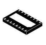
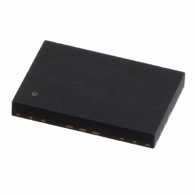
| 产品图片 |
|
| rohs | 符合RoHS无铅 / 符合限制有害物质指令(RoHS)规范要求 |
| 产品系列 | ON Semiconductor CM1233-08DE- |
| 数据手册 | |
| 产品型号 | CM1233-08DE |
| 不同频率时的电容 | - |
| 产品种类 | ESD 抑制器 |
| 供应商器件封装 | 16-WDFN(6x4) |
| 其它名称 | CM1233-08DEOSCT |
| 击穿电压 | 6 V |
| 功率-峰值脉冲 | - |
| 包装 | 剪切带 (CT) |
| 单向通道 | - |
| 双向通道 | 4 |
| 商标 | ON Semiconductor |
| 安装类型 | 表面贴装 |
| 封装 | Reel |
| 封装/外壳 | 16-WDFN 裸露焊盘 |
| 封装/箱体 | TDFN-16 |
| 工作温度 | -40°C ~ 85°C (TA) |
| 工作温度范围 | - 40 C to + 85 C |
| 工作电压 | 5.5 V |
| 工厂包装数量 | 3000 |
| 应用 | 通用 |
| 标准包装 | 1 |
| 电压-击穿(最小值) | 6V |
| 电压-反向关态(典型值) | 5.5V(最小值) |
| 电压-箝位(最大值)@Ipp | 10V (标准) |
| 电流-峰值脉冲(10/1000µs) | 1A (8/20µs) |
| 电流额定值 | 3.2 A |
| 电源线路保护 | 是 |
| 端接类型 | Solder Pad |
| 类型 | 转向装置(轨至轨) |
| 系列 | CM1233 |
| 通道 | 8 Channels |


- 商务部:美国ITC正式对集成电路等产品启动337调查
- 曝三星4nm工艺存在良率问题 高通将骁龙8 Gen1或转产台积电
- 太阳诱电将投资9.5亿元在常州建新厂生产MLCC 预计2023年完工
- 英特尔发布欧洲新工厂建设计划 深化IDM 2.0 战略
- 台积电先进制程称霸业界 有大客户加持明年业绩稳了
- 达到5530亿美元!SIA预计今年全球半导体销售额将创下新高
- 英特尔拟将自动驾驶子公司Mobileye上市 估值或超500亿美元
- 三星加码芯片和SET,合并消费电子和移动部门,撤换高东真等 CEO
- 三星电子宣布重大人事变动 还合并消费电子和移动部门
- 海关总署:前11个月进口集成电路产品价值2.52万亿元 增长14.8%


PDF Datasheet 数据手册内容提取
CM1233 ESD Clamp Array for High Speed Data Line Protection Product Description The CM1233 is ideal for protecting systems with high data and clock rates or for circuits requiring low capacitive loading and tightly http://onsemi.com controlled signal skews (with channel−to−channel matching at 2% max deviation). The device is particularly well−suited for protecting systems using 16 high−speed ports such as DVI or HDMI, along with corresponding ports in removable storage, digital camcorders, DVD−RW drives and 1 other applications where extremely low loading capacitance with ESD protection are required. WDFN16 DE SUFFIX The CM1233 also features easily routed “pass−through” pinouts in a CASE 511AY RoHS compliant (lead−free), 16−lead WDFN, small footprint package. Features PINOUT DIAGRAM • ESD Protection for 4 Pairs of Differential Channels Out_1+ 1 In_1+ • ESD Protection toIEC61000−4−2 Level 4 at ±8 kV Contact Out_1− In_1− Discharge Out_2+ In_2+ • Pass−through Impedance Matched Clamp Architecture Out_2− In_2− GND • Out_3+ In_3+ Flow−through Routing for High−speed Signal Integrity Out_3− In_3− • Minimal Line Capacitance Change with Temperature and Voltage Out_4+ In_4+ • 100 (cid:2) Matched Impedance for Each Paired Differential Channel Out_4− In_4− • Each I/O Pin can Withstand Over 1000 ESD Strikes* (Bottom View) • RoHS Compliant (lead−free) WDFN−16 Package Applications ORDERING INFORMATION • DVI Ports, HDMI Ports in Notebooks, Set Top Boxes, Digital TVs, See detailed ordering and shipping information in the package dimensions section on page 8 of this data sheet. and LCD Displays • General Purpose High−speed Data Line ESD Protection *Standard test condition is IEC61000−4−2 level 4 test circuit with each pin subjected to ±8 kV contact discharge for 1000 pulses. Discharges are timed at 1 second intervals and all 1000 strikes are completed in one continuous test run. The part is then subjected to standard production test to verify that all of the tested parameters are within spec after the 1000 strikes. © Semiconductor Components Industries, LLC, 2014 1 Publication Order Number: January, 2014 − Rev. 4 CM1233/D
CM1233 Figure 1. Electrical Schematic ESD Protection Architecture characteristic impedance that helps optimize 100(cid:2) load Conceptually, an ESD protection device performs the impedance applications such as the HDMI high speed data following actions upon an ESD strike discharge into a lines. protected ASIC (see Figure 2): NOTE: When each of the channels are used individually 1.When an ESD potential is applied to the system for single−ended signal lines protection, the under test (contact or air−discharge), Kirchoff’s individual channel provides 50(cid:2) characteristic Current Law (KCL) dictates that the Electrical impedance matching. Overstress (EOS) currents will immediately divide The load impedance matching feature of the CM1233 throughout the circuit, based on the dynamic helps to simplify system designer’s PCB layout impedance of each path. considerations in impedance matching and also eliminates associated passive components. 2.Ideally, the classic shunt ESD clamp will switch The route through the architecture enables the CM1233 to within 1 ns to a low−impedance path and return provide matched impedance for the signal path between the the majority of the EOS current to the chassis connector and the ASIC. Besides this function, this circuit shield/reference ground. In actuality, if the ESD arrangement also changes the way the parasitic inductance component’s response time (t ) is slower CLAMP interacts with the ESD protection circuit and helps reduce than the ASIC it is protecting, or if the Dynamic the I current to the ASIC. RESIDUAL Clamping Resistance (R ) is not significantly DYN lower than the ASIC’s I/O cell circuitry, then the ASIC will have to absorb a large amount of the EOS energy, and be more likely to fail. 3.Subsequent to the ESD/EOS event, both devices must immediately return to their original specifications, and be ready for an additional strike. Any deterioration in parasitics or clamping capability should be considered a failure, since it can then affect signal integrity or subsequent protection capability. (This is known as “multi−strike” capability.) In the CM1233 architecture, the signal line leading the Figure 2. Standard ESD Protection Device Block connector to the ASIC routes through the CM1233 chip Diagram which provides 100 (cid:2) matched differential channel http://onsemi.com 2
CM1233 The Architecture Advantages leading to the ESD protection element. This limits the speed Figure 3 illustrates a standard ESD protection device. The that the ESD pulse can discharge through the ESD protection inductor element represents the parasitic inductance arising element. from the bond wire and the PCB trace leading to the ESD In the architecture, the inductive elements are in series to protection diodes. the conduction path leading to the protected device. The elements actually help to limit the current and voltage striking the protected device. First the reactance of the inductive element, L1, on the connector side when an ESD strike occurs, acts in the opposite direction of the ESD striking current. This helps limit the peak striking voltage. Then the reactance of the inductive element, L2, on the ASIC side forces this limited ESD strike current to be shunted through the ESD protection diodes. At the same time, the voltage drop across both series element acts to lower the clamping voltage at the protected device terminal. Through this arrangement, the inductive elements also tune the impedance of the ESD protection element by cancelling the capacitive load presented by the ESD diodes Figure 3. Standard ESD Protection Model to the signal line. This improves the signal integrity and Figure 4 illustrates one of the channels. Similarly, the makes the overall ESD protection device more transparent inductor elements represent the parasitic inductance arising to the high bandwidth data signals passing through the from the bond wire and PCB traces leading to the ESD channel. protection diodes as well. The innovative architecture turns the disadvantages of the parasitic inductive elements into useful components that help to limit the ESD current strike to the protected device and also improves the signal integrity of the system by balancing the capacitive loading effects of the ESD diodes. At the same time, this architecture provides an impedance matched signal path for 50 (cid:2) loading applications. Board designs can take advantage of precision internal component matching for improved signal integrity, which is not otherwise possible with discrete components at the system level. This helps to simplify the PCB layout considerations by the system designer and eliminates the Figure 4. CM1233 ESD Protection Model associated passive components for load matching that is normally required with standard ESD protection circuits. CM1233 Inductor Elements In the CM1233 architecture, the inductor elements and Each ESD channel consists of a pair of diodes in series ESD protection diodes interact differently compared to the which steer the positive or negative ESD current pulse to standard ESD model. either the Zener diode or to ground. This embedded Zener In the standard ESD protection device model, the diode also serves to eliminate the need for a separate bypass inductive element presents high impedance against high capacitor to absorb positive ESD strikes to ground. The slew rate strike voltage, i.e. during an ESD strike. The CM1233 protects against ESD pulses up to ±8 kV contact impedance increases the resistance of the conduction path per the IEC 61000−4−2 standard. http://onsemi.com 3
CM1233 PIN DESCRIPTIONS Pin Name Description 1 In_1+ Bidirectional Clamp to ASIC (inside system) 2 In_1− Bidirectional Clamp to ASIC (inside system) 3 In_2+ Bidirectional Clamp to ASIC (inside system) 4 In_2− Bidirectional Clamp to ASIC (inside system) 5 In_3+ Bidirectional Clamp to ASIC (inside system) 6 In_3− Bidirectional Clamp to ASIC (inside system) 7 In_4+ Bidirectional Clamp to ASIC (inside system) 8 In_4− Bidirectional Clamp to ASIC (inside system) 9 Out_4− Bidirectional Clamp to Connector (outside system) 10 Out_4+ Bidirectional Clamp to Connector (outside system) 11 Out_3− Bidirectional Clamp to Connector (outside system) 12 Out_3+ Bidirectional Clamp to Connector (outside system) 13 Out_2− Bidirectional Clamp to Connector (outside system) 14 Out_2+ Bidirectional Clamp to Connector (outside system) 15 Out_1− Bidirectional Clamp to Connector (outside system) 16 Out_1+ Bidirectional Clamp to Connector (outside system) PAD GND Ground return to shield http://onsemi.com 4
CM1233 Specifications Table 1. ABSOLUTE MAXIMUM RATINGS Parameter Rating Units Operating Temperature Range −40 to +85 °C Storage Temperature Range −65 to +150 °C Breakdown Voltage (Positive) 6 V Stresses exceeding those listed in the Maximum Ratings table may damage the device. If any of these limits are exceeded, device functionality should not be assumed, damage may occur and reliability may be affected. Table 2. ELECTRICAL OPERATING CHARACTERISTICS (All parameters specified at TA = –40°C to +85°C unless otherwise noted.) Symbol Parameter Conditions Min Typ Max Units VIN I/O Voltage Relative to GND −0.5 5.5 V IIN Continuous Current through signal pins 100 mA (IN to OUT) 1000 Hr IF Channel Leakage Current TA = 25°C; VN = 5 V ±0.1 ±1.0 (cid:3)A VESD ESD Protection − Peak Discharge Voltage TA = 25°C ±8 kV at any channel input, in system: Contact discharge per IEC 61000−4−2 Standard IRES Residual ESD Peak Current on RDUP IEC 61000−4−2 8 kV; 3.2 A (Resistance of Device Under Protection) RDUP = 5 (cid:2), TA = 25°C; See Figure 7 VCL Channel Clamp Voltage IPP = 1 A, TA = 25°C, V (Channel clamp voltage per tP = 8/20 (cid:3)S IEC 61000−4−5 Standard) Positive Transients +10 Negative Transients −1.8 RDYN Dynamic Resistance IPP = 1 A, TA = 25°C, (cid:2) Positive Transients tP = 8/20 (cid:3)S 0.9 Negative Transients 0.55 Zo Differential Channels pair TR = 200 ps 100 (cid:2) characteristic impedance (cid:4)Zo Channel−to−Channel Impedance Match TR = 200 ps 2 % (Differential) ZCHANNEL Individual Channel Characteristic Imped- TR = 200 ps 50 (cid:2) ance in Single−ended Connection (cid:4)ZCHANNEL Channel−to−Channel Impedance Match TR = 200 ps 2 % (Individual) Product parametric performance is indicated in the Electrical Characteristics for the listed test conditions, unless otherwise noted. Product performance may not be indicated by the Electrical Characteristics if operated under different conditions. http://onsemi.com 5
CM1233 Performance Information Graphical Comparison and Test Setup Figure 5 shows that the CM1233 (ESD protector) lowers the peak voltage and clamping voltage by 45% across a wide range of loading conditions in comparison to a standard ESD protection device. Figure 6 also indicates that the DUP/ASIC protected by the CM1233 dissipates less energy than a standard ESD protection device. This data was derived using the test setups shown in Figure 7. VPEAK Energy (0−50 ns) 1.2 0.6 STD ESD Device 1.0 0.5 STD ESD Device d) d) e e aliz 0.8 aliz 0.4 m m Nor 0.6 CM1233 Nor 0.3 CM1233 E ( Y ( G G LTA 0.4 ER 0.2 O N V E 0.2 0.1 0 0 5 10 20 5 10 20 RDUP ((cid:2)) RDUP ((cid:2)) Figure 5. VPeak (8KV IEC−61000 4−2 ESD Figure 6. Energy Dissipated in DUP vs. RDUP* Contact Strike) and VClamp vs. Loading (RDUP)* *RDUP is the emulated Dynamic Resistance (load) of the Device Under Protection (DUP). See Figure 7. Voltage IEC 61000−4−2 Voltage IEC 61000−4−2 Probe Test Standards Probe Test Standards CM1233 Device Under Device Under Standard Protection (DUP) Protection (DUP) ESD Device RVARIABLE RVARIABLE Current IRESIDUAL Current IRESIDUAL Standard ESD Probe CM1233 Test Setup Probe Device Test Setup Figure 7. Test Setups: Standard Device (Left) and CM1233 (Right) http://onsemi.com 6
CM1233 100.0 (cid:2) Figure 8. Typical Channel TDR Measured Across Out_x and In_x Per Each Differential Channels Pair (Typical 200 ps Incident Rise Time) Application Information CM1233 Application and Guidelines As a general rule, the CM1233 ESD protection array should be located as close as possible to the point of entry of expected electrostatic discharges with minimum PCB trace lengths to the ground planes and between the signal input and the ESD device to minimize stray series inductance. Figure 9. Application of Positive ESD Pulse Between Input Channel and Ground Additional Information See also ON Semiconductor Application Note “Design Considerations for ESD Protection,” in the Applications section at www.onsemi.com. Figure 10. Typical PCB Layout http://onsemi.com 7
CM1233 Ordering Information PART NUMBERING INFORMATION Ordering Part Number Pin Package (Lead−Free Finish) Part Marking 16 WDFN−16 CM1233−08DE CM1233−08 NOTE: Parts are shipped in Tape & Reel form unless otherwise specified. TAPE AND REEL SPECIFICATIONS † Pocket Size (mm) Tape Width Reel Qty per Part Number Package Size (mm) B0 X A0 X K0 W Diameter Reel P0 P1 CM1233 6.00 X 4.00 X 0.75 6.30 X 4.30 X 1.10 12 mm 330 mm (13″) 3000 4 mm 8 mm †For information on tape and reel specifications, including part orientation and tape sizes, please refer to our Tape and Reel Packaging Specifications Brochure, BRD8011/D. http://onsemi.com 8
CM1233 PACKAGE DIMENSIONS WDFN16, 6x4, 0.75P CASE 511AY−01 ISSUE O D A B L L NOTES: 1. DIMENSIONING AND TOLERANCING PER ASME Y14.5M, 1994. 2. CONTROLLING DIMENSION: MILLIMETERS. L1 3. DIMENSION b APPLIES TO PLATED REFEPRINE ONCNEE ÉÉ E DETAIL A T0.E1R5 MAINNDA L0 .A30N DM MIS FMREOAMS UTREERDM IBNEATLW TEIPE.N ÉÉ ALTERNATE TERMINAL 4. COPLANARITY APPLIES TO THE EXPOSED 2X 0.10 C CONSTRUCTIONS PAD AS WELL AS THE TERMINALS. ÉÉ MILLIMETERS DIM MIN MAX 2X 0.10 C TOP VIEW A3 A 0.70 0.80 EXPOSED Cu MOLD CMPD A1 0.00 0.05 ÉÇÉÇÉÇ ÉÇÉÇ A3 0.20 REF 0.10 C DETAIL B (A3) A ÇÇÇ DDb2 50..602.5000 BS05C..3105 A1 E 4.00 BSC DETAIL B E2 1.75 1.85 0.08 C ALTERNATE e 0.75 BSC NOTE 4 SIDE VIEW A1 C SPELAATNIENG CONSTRUCTIONS KL 0.03.570 RE0F.45 L1 −−− 0.15 DETAIL A D2 16XL 1 8 RECOMMENDED E2 SOLDERING FOOTPRINT* 5.26 16X 0.63 K 16 9 16Xb e 0.10 C A B e/2 0.05 C NOTE 3 BOTTOM VIEW 1.96 4.30 16X0.32 0.75 PITCH DIMENSION: MILLIMETERS *For additional information on our Pb−Free strategy and soldering details, please download the ON Semiconductor Soldering and Mounting Techniques Reference Manual, SOLDERRM/D. ON Semiconductor and are registered trademarks of Semiconductor Components Industries, LLC (SCILLC). SCILLC owns the rights to a number of patents, trademarks, copyrights, trade secrets, and other intellectual property. A listing of SCILLC’s product/patent coverage may be accessed at www.onsemi.com/site/pdf/Patent−Marking.pdf. SCILLC reserves the right to make changes without further notice to any products herein. SCILLC makes no warranty, representation or guarantee regarding the suitability of its products for any particular purpose, nor does SCILLC assume any liability arising out of the application or use of any product or circuit, and specifically disclaims any and all liability, including without limitation special, consequential or incidental damages. “Typical” parameters which may be provided in SCILLC data sheets and/or specifications can and do vary in different applications and actual performance may vary over time. All operating parameters, including “Typicals” must be validated for each customer application by customer’s technical experts. SCILLC does not convey any license under its patent rights nor the rights of others. SCILLC products are not designed, intended, or authorized for use as components in systems intended for surgical implant into the body, or other applications intended to support or sustain life, or for any other application in which the failure of the SCILLC product could create a situation where personal injury or death may occur. Should Buyer purchase or use SCILLC products for any such unintended or unauthorized application, Buyer shall indemnify and hold SCILLC and its officers, employees, subsidiaries, affiliates, and distributors harmless against all claims, costs, damages, and expenses, and reasonable attorney fees arising out of, directly or indirectly, any claim of personal injury or death associated with such unintended or unauthorized use, even if such claim alleges that SCILLC was negligent regarding the design or manufacture of the part. SCILLC is an Equal Opportunity/Affirmative Action Employer. This literature is subject to all applicable copyright laws and is not for resale in any manner. PUBLICATION ORDERING INFORMATION LITERATURE FULFILLMENT: N. American Technical Support: 800−282−9855 Toll Free ON Semiconductor Website: www.onsemi.com Literature Distribution Center for ON Semiconductor USA/Canada P.O. Box 5163, Denver, Colorado 80217 USA Europe, Middle East and Africa Technical Support: Order Literature: http://www.onsemi.com/orderlit Phone: 303−675−2175 or 800−344−3860 Toll Free USA/Canada Phone: 421 33 790 2910 Fax: 303−675−2176 or 800−344−3867 Toll Free USA/Canada Japan Customer Focus Center For additional information, please contact your local Email: orderlit@onsemi.com Phone: 81−3−5817−1050 Sales Representative http://onsemi.com CM1233/D 9
Mouser Electronics Authorized Distributor Click to View Pricing, Inventory, Delivery & Lifecycle Information: O N Semiconductor: CM1233-08DE