ICGOO在线商城 > 射频/IF 和 RFID > RFID,RF 接入,监控 IC > CLRC63201T/0FE,112

 Datasheet下载
- 型号: CLRC63201T/0FE,112
- 制造商: NXP Semiconductors
- 库位|库存: xxxx|xxxx
- 要求:
| 数量阶梯 | 香港交货 | 国内含税 |
| +xxxx | $xxxx | ¥xxxx |
查看当月历史价格
查看今年历史价格
CLRC63201T/0FE,112产品简介:
ICGOO电子元器件商城为您提供CLRC63201T/0FE,112由NXP Semiconductors设计生产,在icgoo商城现货销售,并且可以通过原厂、代理商等渠道进行代购。 CLRC63201T/0FE,112价格参考。NXP SemiconductorsCLRC63201T/0FE,112封装/规格:RFID,RF 接入,监控 IC, RFID Reader IC 13.56MHz ISO 14443, ISO 15693, MIFARE SPI 3.3 V ~ 5 V 32-SOIC (0.295", 7.50mm Width)。您可以下载CLRC63201T/0FE,112参考资料、Datasheet数据手册功能说明书,资料中有CLRC63201T/0FE,112 详细功能的应用电路图电压和使用方法及教程。
| 参数 | 数值 |
| 产品目录 | |
| 描述 | IC I.CODE HS READER 32SORFID应答器 I.CODE HS READER |
| 产品分类 | RFID IC集成电路 - IC |
| 品牌 | NXP Semiconductors |
| 产品手册 | |
| 产品图片 |
|
| rohs | 符合RoHS无铅 / 符合限制有害物质指令(RoHS)规范要求 |
| 产品系列 | RF集成电路,RFID应答器,NXP Semiconductors CLRC63201T/0FE,112I-Code |
| 数据手册 | |
| 产品型号 | CLRC63201T/0FE,112 |
| PCN封装 | |
| RF类型 | 只读 |
| 产品目录页面 | |
| 产品种类 | RFID应答器 |
| 供应商器件封装 | 32-SO |
| 其它名称 | 568-2199-5 |
| 其它有关文件 | |
| 功能 | Read Only |
| 包装 | 管件 |
| 商标 | NXP Semiconductors |
| 存储容量 | 3072 bit |
| 安装风格 | SMD/SMT |
| 封装 | Tube |
| 封装/外壳 | 32-SOIC(0.295",7.50mm 宽) |
| 封装/箱体 | SOIC-32 |
| 工作温度范围 | - 25 C to + 85 C |
| 工厂包装数量 | 960 |
| 最大工作温度 | + 85 C |
| 最小工作温度 | - 25 C |
| 标准包装 | 24 |
| 特性 | ISO14443-A,ISO14443-B,ISO15693,ISO18000-3 |
| 系列 | CLRC632 |
| 零件号别名 | CLRC63201TD |
| 频率 | 13.56 MHz |


- 商务部:美国ITC正式对集成电路等产品启动337调查
- 曝三星4nm工艺存在良率问题 高通将骁龙8 Gen1或转产台积电
- 太阳诱电将投资9.5亿元在常州建新厂生产MLCC 预计2023年完工
- 英特尔发布欧洲新工厂建设计划 深化IDM 2.0 战略
- 台积电先进制程称霸业界 有大客户加持明年业绩稳了
- 达到5530亿美元!SIA预计今年全球半导体销售额将创下新高
- 英特尔拟将自动驾驶子公司Mobileye上市 估值或超500亿美元
- 三星加码芯片和SET,合并消费电子和移动部门,撤换高东真等 CEO
- 三星电子宣布重大人事变动 还合并消费电子和移动部门
- 海关总署:前11个月进口集成电路产品价值2.52万亿元 增长14.8%


PDF Datasheet 数据手册内容提取
CLRC632 Standard multi-protocol reader solution Rev. 3.7 — 27 February 2014 Product data sheet 073937 COMPANY PUBLIC 1. Introduction This data sheet describes the functionality of the CLRC632 Integrated Circuit (IC). It includes the functional and electrical specifications and from a system and hardware viewpoint gives detailed information on how to design-in the device. Remark: The CLRC632 supports all variants of the MIFARE Mini, MIFARE 1K, MIFARE4K and MIFARE Ultralight RF identification protocols. To aid readability throughout this data sheet, the MIFARE Mini, MIFARE 1K, MIFARE 4K and MIFAREUltralight products and protocols have the generic name MIFARE. 2. General description The CLRC632 is a highly integrated reader IC for contactless communication at 13.56MHz. The CLRC632 reader IC provides: • outstanding modulation and demodulation for passive contactless communication • a wide range of methods and protocols • a small, fully integrated package • pin compatibility with the MFRC500, MFRC530, MFRC531 and SLRC400 All protocol layers of the ISO/IEC 14443A and ISO/IEC 14443B communication standards are supported provided: • additional components, such as the oscillator, power supply, coil etc. are correctly applied. • standardized protocols, such as ISO/IEC 14443-4 and/or ISO/IEC 14443 B anticollision are correctly implemented The CLRC632 supports contactless communication using MIFARE higher baud rates (see Section9.12 on page40). The receiver module provides a robust and efficient demodulation/decoding circuitry implementation for compatible transponder signals (see Section9.10 on page34). The digital module, manages the complete ISO/IEC 14443 standard framing and error detection (parity and CRC). In addition, it supports the fast MIFARE security algorithm for authenticating the MIFARE products (see Section9.14 on page42). All layers of the I-CODE1 and ISO/IEC 15693 protocols are supported by the CLRC632. The receiver module provides a robust and efficient demodulation/decoding circuitry implementation for I-CODE1 and ISO/IEC 15693 compatible transponder signals. The digital module handles I-CODE1 and ISO/IEC 15693 framing and error detection (CRC).
CLRC632 NXP Semiconductors Standard multi-protocol reader solution The internal transmitter module (Section9.9 on page31) can directly drive an antenna designed for a proximity operating distance up to 100 mm without any additional active circuitry. A parallel interface can be directly connected to any 8-bit microprocessor to ensure reader/terminal design flexibility. In addition, Serial Peripheral Interface (SPI) compatibility is supported (see Section9.1.4 on page9). 3. Features and benefits 3.1 General Highly integrated analog circuitry for demodulating and decoding card/label response Buffered output drivers enable antenna connection using the minimum of external components Proximity operating distance up to 100 mm Supports both ISO/IEC 14443 A and ISO/IEC 14443 B standards Supports MIFARE dual-interface card ICs and the MIFAREMini, MIFARE1K, MIFARE4K protocols Contactless communication at MIFARE higher baud rates (up to 424 kBd) Supports both I-CODE1 and ISO/IEC 15693 protocols Crypto1 and secure non-volatile internal key memory Pin-compatible with the MFRC500, MFRC530, MFRC531 and the SLRC400 Parallel microprocessor interface with internal address latch and IRQ line SPI compatibility Flexible interrupt handling Automatic detection of parallel microprocessor interface type 64-byte send and receive FIFO buffer Hard reset with low power function Software controlled Power-down mode Programmable timer Unique serial number User programmable start-up configuration Bit-oriented and byte oriented framing Independent power supply pins for analog, digital and transmitter modules Internal oscillator buffer optimized for low phase jitter enables 13.56 MHz quartz connection Clock frequency filtering 3.3 V to 5 V operation for transmitter in short range and proximity applications 3.3 V or 5 V operation for the digital module 4. Applications Electronic payment systems Identification systems Access control systems CLRC632 All information provided in this document is subject to legal disclaimers. © NXP Semiconductors N.V. 2014. All rights reserved. Product data sheet Rev. 3.7 — 27 February 2014 COMPANY PUBLIC 073937 2 of 127
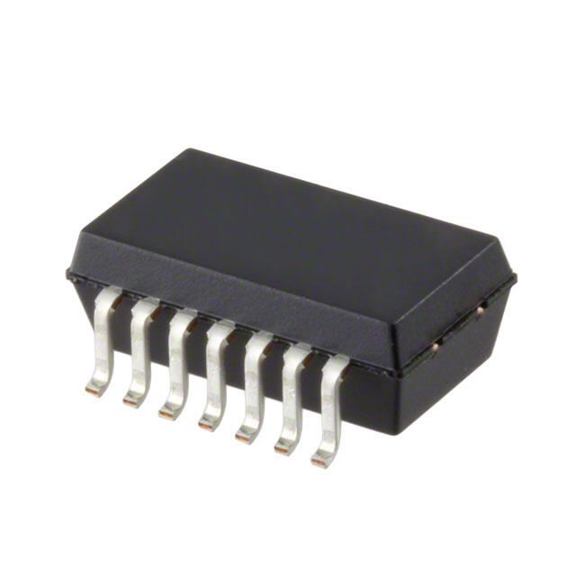
CLRC632 NXP Semiconductors Standard multi-protocol reader solution Subscriber services Banking systems Digital content systems 5. Quick reference data Table 1. Quick refere nce data Symbol Parameter Conditions Min Typ Max Unit T ambient temperature 40 - +150 C amb T storage temperature 40 - +150 C stg V digital supply voltage 0.5 5 6 V DDD V analog supply voltage 0.5 5 6 V DDA V TVDD supply voltage 0.5 5 6 V DD(TVDD) V input voltage (absolute on any digital pin to DVSS 0.5 - V + 0.5 V i DDD value) on pin RX to AVSS 0.5 - V + 0.5 V DDA I input leakage current 1.0 - 1.0 mA LI I TVDD supply current continuous wave - - 150 mA DD(TVDD) 6. Ordering information Table 2. Ordering info rmation Type number Package Name Description Version CLRC63201T/0FE SO32 plastic small outline package; 32 leads; body width 7.5 mm SOT287-1 CLRC632 All information provided in this document is subject to legal disclaimers. © NXP Semiconductors N.V. 2014. All rights reserved. Product data sheet Rev. 3.7 — 27 February 2014 COMPANY PUBLIC 073937 3 of 127
CLRC632 NXP Semiconductors Standard multi-protocol reader solution 7. Block diagram NWR NRD NCS ALE A0 A1 A2 AD0 to AD7/D0 to D7 10 11 9 21 22 23 24 13 14 15 16 17 18 19 20 PARALLEL INTERFACE CONTROL VOLTAGE 25 DVDD (INCLUDING AUTOMATIC INTERFACE DETECTION AND SYNCHRONISATION) MONITOR AND POWER ON 12 DVSS DETECT FIFO CONTROL STATE MACHINE 64-BYTE FIFO COMMAND REGISTER RESET CONTROL PROGRAMMABLE TIMER POWER DOWN 31 CONTROL REGISTER RSTPD CONTROL BANK 2 INTERRUPT CONTROL IRQ CRC16/CRC8 32 × 16-BYTE EEPROM GENERATION AND CHECK ACCESS EEPROM CONTROL PARALLEL/SERIAL CONVERTER BIT COUNTER MASTER KEY BUFFER PARITY GENERATION AND CHECK FRAME GENERATION AND CHECK CRYPTO1 UNIT BIT DECODING BIT ENCODING 32-BIT PSEUDO 3 RANDOM GENERATOR MFIN SERIAL DATA SWITCH 4 MFOUT LEVEL SHIFTERS 1 AMPLITUDE CLOCK OSCIN RATING CORRELATION GENERATION, OSCILLATOR AND FILTERING AND 32 REFERENCE BIT DECODING DISTRIBUTION OSCOUT VOLTAGE 26 Q-CLOCK POWER ON AVDD 28 I-CHANNEL Q-CHANNEL GENERATION DETECT AVSS ANALOG AMPLIFIER AMPLIFIER TEST MULTIPLEXER I-CHANNEL Q-CHANNEL TRANSMITTER CONTROL DEMODULATOR DEMODULATOR GND V GND V 30 27 29 8 5 7 6 VMID AUX RX TVSS TX1 TX2 TVDD 001aaj629 Fig 1. CLRC632 block diagram CLRC632 All information provided in this document is subject to legal disclaimers. © NXP Semiconductors N.V. 2014. All rights reserved. Product data sheet Rev. 3.7 — 27 February 2014 COMPANY PUBLIC 073937 4 of 127
CLRC632 NXP Semiconductors Standard multi-protocol reader solution 8. Pinning information OSCIN 1 32 OSCOUT IRQ 2 31 RSTPD MFIN 3 30 VMID MFOUT 4 29 RX TX1 5 28 AVSS TVDD 6 27 AUX TX2 7 26 AVDD TVSS 8 25 DVDD CLRC632 NCS 9 24 A2/SCK NWR/R/NW/nWrite 10 23 A1 NRD/NDS/nDStrb 11 22 A0/nWait/MOSI DVSS 12 21 ALE/AS/nAStrb/NSS AD0/D0 13 20 D7/AD7 AD1/D1 14 19 D6/AD6 AD2/D2 15 18 D5/AD5 AD3/D3 16 17 D4/AD4 001aaj630 Fig 2. CLRC632 pin configuration 8.1 Pin description Table 3. Pin descripti on Pin Symbol Type[1] Description 1 OSCIN I oscillator/clock inputs: crystal oscillator input to the oscillator’s inverting amplifier externally generated clock input; f = 13.56 MHz osc 2 IRQ O interrupt request generates an output signaling an interrupt event 3 MFIN I ISO/IEC14443A MIFARE serial data interface input 4[2] MFOUT O interface outputs used as follows: MIFARE: generates serial data ISO/IEC14443A I-CODE: generates serial data based on I-CODE1 and ISO/IEC15693 5 TX1 O transmitter 1 modulated carrier output; 13.56 MHz 6 TVDD P transmitter power supply for the TX1 and TX2 output stages 7 TX2 O transmitter 2 modulated carrier output; 13.56 MHz 8 TVSS G transmitter ground for the TX1 and TX2 output stages 9 NCS I not chip select input is used to select and activate the CLRC632’s microprocessor interface 10[3] NWR I not write input generates the strobe signal for writing data to the CLRC632 registers when applied to pins D0 to D7 R/NW I read not write input is used to switch between read or write cycles nWrite I not write input selects the read or write cycle to be performed CLRC632 All information provided in this document is subject to legal disclaimers. © NXP Semiconductors N.V. 2014. All rights reserved. Product data sheet Rev. 3.7 — 27 February 2014 COMPANY PUBLIC 073937 5 of 127
CLRC632 NXP Semiconductors Standard multi-protocol reader solution Table 3. Pin description …continued Pin Symbol Type[1] Description 11[3] NRD I not read input generates the strobe signal for reading data from the CLRC632 registers when applied to pins D0 to D7 NDS I not data strobe input generates the strobe signal for the read and write cycles nDStrb I not data strobe input generates the strobe signal for the read and write cycles 12 DVSS G digital ground 13 D0 O SPI master in, slave out output 13 to 20[3] D0 to D7 I/O 8-bit bidirectional data bus input/output on pins D0 to D7 AD0 to AD7 I/O 8-bit bidirectional address and data bus input/output on pins AD0 to AD7 21[3] ALE I address latch enable input for pins AD0 to AD5; HIGH latches the internal address AS I address strobe input for pins AD0 to AD5; HIGH latches the internal address nAStrb I not address strobe input for pins AD0 to AD5; LOW latches the internal address NSS I not slave select strobe input for SPI communication 22[3] A0 I address line 0 is the address register bit 0 input nWait O not wait output: LOW starts an access cycle HIGH ends an access cycle MOSI I SPI master out, slave in 23 A1 I address line 1 is the address register bit 1 input 24[3] A2 I address line 2 is the address register bit 2 input SCK I SPI serial clock input 25 DVDD P digital power supply 26 AVDD P analog power supply for pins OSCIN, OSCOUT, RX, VMID and AUX 27 AUX O auxiliary output is used to generate analog test signals. The output signal is selected using the TestAnaSelect register’s TestAnaOutSel[4:0] bits 28 AVSS G analog ground 29 RX I receiver input is used as the card response input. The carrier is load modulated at 13.56 MHz, drawn from the antenna circuit 30 VMID P internal reference voltage pin provides the internal reference voltage as a supply Remark: It must be connected to a 100 nF block capacitor connected between pin VMID and ground 31 RSTPD I reset and power-down input: HIGH: the internal current sinks are switched off, the oscillator is inhibited and the input pads are disconnected LOW (negative edge): start internal reset phase 32 OSCOUT O crystal oscillator output for the oscillator’s inverting amplifier [1] Pin types: I=Input, O=Output, I/O=Input/Output, P=Power and G=Ground. [2] The SLRC400 uses pin name SIGOUT for pin MFOUT. The CLRC632 functionality includes test functions for the SLRC400 using pin MFOUT. [3] These pins provide different functionality depending on the selected microprocessor interface type (see Section9.1 on page7 for detailed information). CLRC632 All information provided in this document is subject to legal disclaimers. © NXP Semiconductors N.V. 2014. All rights reserved. Product data sheet Rev. 3.7 — 27 February 2014 COMPANY PUBLIC 073937 6 of 127
CLRC632 NXP Semiconductors Standard multi-protocol reader solution 9. Functional description 9.1 Digital interface 9.1.1 Overview of supported microprocessor interfaces The CLRC632 supports direct interfacing to various 8-bit microprocessors. Alternatively, the CLRC632 can be connected to a PC’s Enhanced Parallel Port (EPP). Table4 shows the parallel interface signals supported by the CLRC632. Table 4. Supported microprocessor and EPP interface signals Bus control signals Bus Separated address Multiplexed address and data bus and data bus Separated read and control NRD, NWR, NCS NRD, NWR, NCS, ALE write strobes address A0, A1, A2 AD0, AD1, AD2, AD3, AD4, AD5 data D0 to D7 AD0 to AD7 Common read and write control R/NW, NDS, NCS R/NW, NDS, NCS, AS strobe address A0, A1, A2 AD0, AD1, AD2, AD3, AD4, AD5 data D0 to D7 AD0 to AD7 Common read and write control - nWrite, nDStrb, nAStrb, nWait strobe with handshake (EPP) address - AD0, AD1, AD2, AD3, AD4, AD5 data - AD0 to AD7 9.1.2 Automatic microprocessor interface detection After a Power-On or Hard reset, the CLRC632 resets parallel microprocessor interface mode and detects the microprocessor interface type. The CLRC632 identifies the microprocessor interface using the logic levels on the control pins. This is performed using a combination of fixed pin connections and the dedicated Initialization routine (see Section9.7.4 on page30). CLRC632 All information provided in this document is subject to legal disclaimers. © NXP Semiconductors N.V. 2014. All rights reserved. Product data sheet Rev. 3.7 — 27 February 2014 COMPANY PUBLIC 073937 7 of 127
CLRC632 NXP Semiconductors Standard multi-protocol reader solution 9.1.3 Connection to different microprocessor types The connection to various microprocessor types is shown in Table5. Table 5. Connection scheme for detecting the parallel interface type CLRC632 Parallel interface type and signals pins Separated read/write strobe Common read/write strobe Dedicated Multiplexed Dedicated Multiplexed Multiplexed address bus address address bus address bus address bus with bus handshake ALE HIGH ALE HIGH AS nAStrb A2 A2 LOW A2 LOW HIGH A1 A1 HIGH A1 HIGH HIGH A0 A0 HIGH A0 LOW nWait NRD NRD NRD NDS NDS nDStrb NWR NWR NWR R/NW R/NW nWrite NCS NCS NCS NCS NCS LOW D7 to D0 D7 to D0 AD7 to AD0 D7 to D0 AD7 to AD0 AD7 to AD0 9.1.3.1 Separate read and write strobe address bus (A3 to An) DEVICE non-multiplexed address DEVICE ADDRESS ADDRESS NCS NCS DECODER DECODER LOW A2 HIGH address bus (A0 to A2) A1 A0 to A2 HIGH A0 data bus (D0 to D7) multiplexed address/data (AD0 to AD7) D0 to D7 AD0 to AD7 HIGH address latch enable (ALE) ALE ALE Read strobe (NRD) Read strobe (NRD) NRD NRD Write strobe (NWR) Write strobe (NWR) NWR NWR 001aak607 Fig 3. Connection to microprocessor: separate read and write strobes Refer to Section13.4.1 on page102 for timing specification. CLRC632 All information provided in this document is subject to legal disclaimers. © NXP Semiconductors N.V. 2014. All rights reserved. Product data sheet Rev. 3.7 — 27 February 2014 COMPANY PUBLIC 073937 8 of 127
CLRC632 NXP Semiconductors Standard multi-protocol reader solution 9.1.3.2 Common read and write strobe address bus (A3 to An) DEVICE non-multiplexed address DEVICE ADDRESS ADDRESS NCS NCS DECODER DECODER LOW A2 HIGH address bus (A0 to A2) A1 A0 to A2 LOW A0 data bus (D0 to D7) multiplexed address/data (AD0 to AD7) D0 to D7 AD0 to AD7 HIGH Address strobe (AS) ALE ALE Data strobe (NDS) Data strobe (NDS) NRD NRD Read/Write (R/NW) Read/Write (R/NW) NWR NWR 001aak608 Fig 4. Connection to microprocessor: common read and write strobes Refer to Section13.4.2 on page103 for timing specification. 9.1.3.3 Common read and write strobe: EPP with handshake DEVICE LOW NCS HIGH A2 HIGH A1 nWait A0 multiplexed address/data (AD0 to AD7) AD0 to AD7 Address strobe (nAStrb) ALE Data strobe (nDStrb) NRD Read/Write (nWrite) NWR 001aak609 Fig 5. Connection to microprocessor: EPP common read/write strobes and handshake Refer to Section13.4.3 on page104 for timing specification. Remark: In the EPP standard a chip select signal is not defined. To cover this situation, the status of the NCS pin can be used to inhibit the nDStrb signal. If this inhibitor is not used, it is mandatory that pin NCS is connected to pin DVSS. Remark: After each Power-On or Hard reset, the nWait signal on pin A0 is high-impedance. nWait is defined as the first negative edge applied to the nAStrb pin after the reset phase. The CLRC632 does not support Read Address Cycle. 9.1.4 Serial Peripheral Interface The CLRC632 provides compatibility with the 5-wire Serial Peripheral Interface (SPI) standard and acts as a slave during the SPI communication. The SPI clock signal SCK must be generated by the master. Data communication from the master to the slave uses the MOSI line. The MISO line sends data from the CLRC632 to the master. CLRC632 All information provided in this document is subject to legal disclaimers. © NXP Semiconductors N.V. 2014. All rights reserved. Product data sheet Rev. 3.7 — 27 February 2014 COMPANY PUBLIC 073937 9 of 127
CLRC632 NXP Semiconductors Standard multi-protocol reader solution Table 6. SPI compatibility CLRC632 pins SPI pins ALE NSS A2 SCK A1 LOW A0 MOSI NRD HIGH NWR HIGH NCS LOW D7 to D1 do not connect D0 MISO Figure6 shows the microprocessor connection to the CLRC632 using SPI. DEVICE LOW NCS SCK A2 LOW A1 MOSI A0 MISO D0 NSS ALE 001aak610 Fig 6. Connection to microprocessor: SPI Remark: The SPI implementation for CLRC632 conforms to the SPI standard and ensures that the CLRC632 can only be addressed as a slave. 9.1.4.1 SPI read data The structure shown in Table7 must be used to read data using SPI. It is possible to read up to n-data bytes. The first byte sent defines both, the mode and the address. Table 7. SPI read data Pin Byte 0 Byte 1 Byte 2 ... Byte n Byte n + 1 MOSI address 0 address 1 address 2 ... address n 00 MISO XX data 0 data 1 ... data n 1 data n The address byte must meet the following criteria: • the Most Significant Bit (MSB) of the first byte sets the mode. To read data from the CLRC632 the MSB is set to logic 1 • bits [6:1] define the address • the Least Significant Bit (LSB) should be set to logic 0. As shown in Table8, all the bits of the last byte sent are set to logic 0. CLRC632 All information provided in this document is subject to legal disclaimers. © NXP Semiconductors N.V. 2014. All rights reserved. Product data sheet Rev. 3.7 — 27 February 2014 COMPANY PUBLIC 073937 10 of 127
CLRC632 NXP Semiconductors Standard multi-protocol reader solution Table 8. SPI read address Address Bit 7 Bit 6 Bit 5 Bit 4 Bit 3 Bit 2 Bit 1 Bit 0 (MOSI) (MSB) (LSB) byte 0 1 address address address address address address reserved byte 1 to byte n reserved address address address address address address reserved byte n + 1 0 0 0 0 0 0 0 0 [1] All reserved bits must be set to logic 0. 9.1.4.2 SPI write data The structure shown in Table9 must be used to write data using SPI. It is possible to write up to n-data bytes. The first byte sent defines both the mode and the address. Table 9. SPI write data Byte 0 Byte 1 Byte 2 ... Byte n Byte n + 1 MOSI address data 0 data 1 ... data n 1 data n MISO XX XX XX ... XX XX The address byte must meet the following criteria: • the MSB of the first byte sets the mode. To write data to the CLRC632, the MSB is set to logic 0 • bits [6:1] define the address • the LSB should be set to logic 0. SPI write mode writes all data to the address defined in byte 0 enabling effective write cycles to the FIFO buffer. T able 10. SPI write address Address line Bit 7 Bit 6 Bit 5 Bit 4 Bit 3 Bit 2 Bit 1 Bit 0 (MOSI) (MSB) (LSB) byte 0 0 address address address address address address reserved byte 1 to byte data data data data data data data data n+1 [1] All reserved bits must be set to logic 0. Remark: The data bus pins D7 to D0 must be disconnected. Refer to Section13.4.4 on page106 for the timing specification. CLRC632 All information provided in this document is subject to legal disclaimers. © NXP Semiconductors N.V. 2014. All rights reserved. Product data sheet Rev. 3.7 — 27 February 2014 COMPANY PUBLIC 073937 11 of 127
CLRC632 NXP Semiconductors Standard multi-protocol reader solution 9.2 Memory organization of the EEPROM Table 11. EEPROM memory organization diagram Block Byte Access Memory content Refer to address Position Address 0 0 00h to 0Fh R product Section9.2.1 on page13 information field 1 1 10h to 1Fh R/W StartUp register Section9.2.2.1 on page14 initialization file 2 2 20h to 2Fh R/W 3 3 30h to 3Fh R/W register Section 9.2.2.3 “Register initialization file initialization file (read/write)” 4 4 40h to 4Fh R/W on page 16 user data or 5 5 50h to 5Fh R/W second 6 6 60h to 6Fh R/W initialization 7 7 70h to 7Fh R/W 8 8 80h to 8Fh W keys for Crypto1 Section9.2.3 on page18 9 9 90h to 9Fh W 10 A A0h to AFh W 11 B B0h to BFh W 12 C C0h to CFh W 13 D D0h to DFh W 14 E E0h to EFh W 15 F F0h to FFh W 16 10 100h to 10Fh W 17 11 110h to 11Fh W 18 12 120h to 12Fh W 19 13 130h to 13Fh W 20 14 140h to 14Fh W 21 15 150h to 15Fh W 22 16 160h to 16Fh W 23 17 170h to 17Fh W 24 18 180h to 18Fh W 25 19 190h to 19Fh W 26 1A 1A0h to W 1AFh 27 1B 1B0h to W 1BFh 28 1C 1C0h to W 1CFh 29 1D 1D0h to W 1DFh 30 1E 1E0h to W 1EFh 31 1F 1F0h to W 1FFh CLRC632 All information provided in this document is subject to legal disclaimers. © NXP Semiconductors N.V. 2014. All rights reserved. Product data sheet Rev. 3.7 — 27 February 2014 COMPANY PUBLIC 073937 12 of 127
CLRC632 NXP Semiconductors Standard multi-protocol reader solution 9.2.1 Product information field (read only) Table 12. Product information field Byte Symbol Access Value Description 15 CRC R - the content of the product information field is secured using a CRC byte which is checked during start-up 14 RsMaxP R - maximum source resistance for the p-channel driver transistor on pins TX1 and TX2 The source resistance of the p-channel driver transistors of pin TX1 and TX2 can be adjusted using the value GsCfgCW[5:0] in the CwConductance register (see Section9.9.3 on page32). The mean value of the maximum adjustable source resistance for pins TX1 and TX2 is stored as an integer value in in this byte. Typical values for RsMaxP are between 60 to 140. This value is denoted as maximum adjustable source resistance R and S(ref)maxP is measured by setting the CwConductance register’s GsCfgCW[5:0] bits to 01h. 13 to 12 Internal R - two bytes for internal trimming parameters 11 to 8 Product Serial Number R - a unique four byte serial number for the device 7 to 5 reserved R - 4 to 0 Product Type R - the CLRC632 is a member of a new family Identification of highly integrated reader ICs. Each member of the product family has a unique product type identification. The value of the product type identification is shown in Table13. Table 13. Product type identification definition Definition Product type identification bytes Byte 0 1 2 3 4[1] Value 30h FFh FFh 0Fh XXh [1] Byte 4 contains the current version number. 9.2.2 Register initialization files (read/write) Register initialization from address 10h to address 2Fh is performed automatically during the initializing phase (see Section9.7.3 on page30) using the StartUp register initialization file. In addition, the CLRC632 registers can be initialized using values from the register initialization file when the LoadConfig command is executed (see Section11.5.1 on page95). CLRC632 All information provided in this document is subject to legal disclaimers. © NXP Semiconductors N.V. 2014. All rights reserved. Product data sheet Rev. 3.7 — 27 February 2014 COMPANY PUBLIC 073937 13 of 127
CLRC632 NXP Semiconductors Standard multi-protocol reader solution Remark: The following points apply to initialization: • the Page register (addressed using 10h, 18h, 20h, 28h) is skipped and not initialized. • make sure that all PreSetxx registers are not changed. • make sure that all register bits that are reserved are set to logic 0. 9.2.2.1 StartUp register initialization file (read/write) The EEPROM memory block address 1 and 2 contents are used to automatically set the register subaddresses 10h to 2Fh during the initialization phase. The default values stored in the EEPROM during production are shown in Section 9.2.2.2 “Factory default StartUp register initialization file”. The byte assignment is shown in Table14. Table 14. Byte assignment for register initialization at start-up EEPROM byte address Register address Remark 10h (block 1, byte 0) 10h skipped 11h 11h copied … … … 2Fh (block 2, byte 15) 2Fh copied 9.2.2.2 Factory default StartUp register initialization file During the production tests, the StartUp register initialization file is initialized using the default values shown in Table15. During each power-up and initialization phase, these values are written to the CLRC632’s registers. CLRC632 All information provided in this document is subject to legal disclaimers. © NXP Semiconductors N.V. 2014. All rights reserved. Product data sheet Rev. 3.7 — 27 February 2014 COMPANY PUBLIC 073937 14 of 127
CLRC632 NXP Semiconductors Standard multi-protocol reader solution Table 15. Shipment co ntent of StartUp configuration file EEPROM Register Value Symbol Description byte address address 10h 10h 00h Page free for user 11h 11h 58h TxControl transmitter pins TX1 and TX2 are switched off, bridge driver configuration, modulator driven from internal digital circuitry 12h 12h 3Fh CwConductance source resistance of TX1 and TX2 is set to minimum 13h 13h 3Fh ModConductance defines the output conductance 14h 14h 19h CoderControl ISO/IEC 14443A coding is set 15h 15h 13h ModWidth pulse width for Miller pulse coding is set to standard configuration 16h 16h 3Fh ModWidthSOF pulse width of Start Of Frame (SOF) 17h 17h 3Bh TypeFraming ISO/IEC 14443A framing is set 18h 18h 00h Page free for user 19h 19h 73h RxControl1 ISO/IEC 14443A is set and internal amplifier gain is maximum 1Ah 1Ah 08h DecoderControl bit-collisions always evaluate to HIGH in the data bit stream 1Bh 1Bh ADh BitPhase BitPhase[7:0] is set to standard configuration 1Ch 1Ch FFh RxThreshold MinLevel[3:0] and CollLevel[3:0] are set to maximum 1Dh 1Dh 1Eh BPSKDemControl ISO/IEC 14443A is set 1Eh 1Eh 41h RxControl2 use Q-clock for the receiver, automatic receiver off is switched on, decoder is driven from internal analog circuitry 1Fh 1Fh 00h ClockQControl automatic Q-clock calibration is switched on 20h 20h 00h Page free for user 21h 21h 06h RxWait frame guard time is set to six bit-clocks 22h 22h 03h ChannelRedundancy channel redundancy is set using ISO/IEC14443A 23h 23h 63h CRCPresetLSB CRC preset value is set using ISO/IEC 14443A 24h 24h 63h CRCPresetMSB CRC preset value is set using ISO/IEC 14443A 25h 25h 00h TimeSlotPeriod defines the time for the I-CODE1 time slots 26h 26h 00h MFOUTSelect pin MFOUT is set LOW 27h 27h 00h PreSet27 - 28h 28h 00h Page free for user 29h 29h 08h FIFOLevel WaterLevel[5:0] FIFO buffer warning level is set to standard configuration 2Ah 2Ah 07h TimerClock TPreScaler[4:0] is set to standard configuration, timer unit restart function is switched off 2Bh 2Bh 06h TimerControl Timer is started at the end of transmission, stopped at the beginning of reception 2Ch 2Ch 0Ah TimerReload TReloadValue[7:0]: the timer unit preset value is set to standard configuration 2Dh 2Dh 02h IRQPinConfig pin IRQ is set to high-impedance 2Eh 2Eh 00h PreSet2E - 2Fh 2Fh 00h PreSet2F - Remark: The CLRC632 default configuration supports the MIFARE and ISO/IEC14443 A communication scheme. Memory addresses 3 to 7 may be used for user-specific initialization files such as I-CODE1, ISO/IEC 15693 or ISO/IEC 14443 B. CLRC632 All information provided in this document is subject to legal disclaimers. © NXP Semiconductors N.V. 2014. All rights reserved. Product data sheet Rev. 3.7 — 27 February 2014 COMPANY PUBLIC 073937 15 of 127
CLRC632 NXP Semiconductors Standard multi-protocol reader solution 9.2.2.3 Register initialization file (read/write) The EEPROM memory content from block address 3 to 7 can initialize register sub addresses 10h to 2Fh when the LoadConfig command is executed (see Section11.5.1 on page95). This command requires the EEPROM starting byte address as a two byte argument for the initialization procedure. The byte assignment is shown in Table16. Table 16. Byte assignment for register initialization at startup EEPROM byte address Register address Remark EEPROM starting byte address 10h skipped EEPROM + 1 starting byte address 11h copied … … EEPROM + 31 starting byte address 2Fh copied The register initialization file is large enough to hold values for two initialization sets and up to one block (16-byte) of user data. The startup configuration could be adapted to the I-CODE1 StartUp configuration and stored in register block address 3 and 4, providing additional flexibility. Remark: The register initialization file can be read/written by users and these bytes can be used to store other user data. After each power-up, the default configuration enables the MIFARE and ISO/IEC 14443A protocol. 9.2.2.4 Content of I-CODE1 and ISO/IEC 15693 StartUp register values Table17 gives an overview of the StartUp values for I-CODE1 and ISO/IEC15693 communication. CLRC632 All information provided in this document is subject to legal disclaimers. © NXP Semiconductors N.V. 2014. All rights reserved. Product data sheet Rev. 3.7 — 27 February 2014 COMPANY PUBLIC 073937 16 of 127
CLRC632 NXP Semiconductors Standard multi-protocol reader solution Table 17. Content of I- CODE1 startup configuration EEPROM Register Value Symbol Description byte address address 30h 10h 00h Page free for user 31h 11h 58h TxControl transmitter pins TX1 and TX2 switched off, bridge driver configuration, modulator driven from internal digital circuitry 32h 12h 3Fh CwConductance source resistance (R ) of TX1 and TX2 to minimum S 33h 13h 05h ModGsCfgh source resistance (R ) of TX1 and TX2 at the time of S modulation, to determine the modulation index 34h 14h 2Ch CoderControl selects the bit coding mode and the framing during transmission 35h 15h 3Fh ModWidth pulse width for code used (1 out of 256, NRZ or 1 out of 4) pulse coding is set to standard configuration 36h 16h 3Fh ModWidthSOF pulse width of SOF 37h 17h 00h TypeBFraming - 38h 18h 00h Page free for user 39h 19h 8Bh RxControl1 amplifier gain is maximum 3Ah 1Ah 00h DecoderControl bit-collisions always evaluate to HIGH in the data bit stream 3Bh 1Bh 54h BitPhase BitPhase[7:0] is set to standard configuration 3Ch 1Ch 68h RxThreshold: MinLevel[3:0] and CollLevel[3:0] are set to maximum 3Dh 1Dh 00h BPSKDemControl - 3Eh 1Eh 41h RxControl2 use Q-clock for the receiver, automatic receiver off is switched on, decoder is driven from internal analog circuitry 3Fh 1Fh 00h ClockQControl automatic Q-clock calibration is switched on 40h 20h 00h Page free for user 41h 21h 08h RxWait frame guard time is set to eight bit-clocks 42h 22h 0Ch ChannelRedundancy channel redundancy is set using I-CODE1 43h 23h FEh CRCPresetLSB CRC preset value is set using I-CODE1 44h 24h FFh CRCPresetMSB CRC preset value is set using I-CODE1 45h 25h 00h TimeSlot Period defines the time for the I-CODE1 time slots 46h 26h 00h MFOUTSelect pin MFOUT is set LOW 47h 27h 00h PreSet27 - 48h 28h 00h Page free for user 49h 29h 3Eh FIFOLevel WaterLevel[5:0] FIFO buffer warning level is set to standard configuration 4Ah 2Ah 0Bh TimerClock TPreScaler[4:0] is set to standard configuration, timer unit restart function is switched off 4Bh 2Bh 02h TimerControl Timer is started at the end of transmission, stopped at the beginning of reception 4Ch 2Ch 00h TimerReload the timer unit preset value is set to standard configuration 4Dh 2Dh 02h IRQPinConfig pin IRQ is set to high-impedance 4Eh 2Eh 00h PreSet2E - 4Fh 2Fh 00h PreSet2F - CLRC632 All information provided in this document is subject to legal disclaimers. © NXP Semiconductors N.V. 2014. All rights reserved. Product data sheet Rev. 3.7 — 27 February 2014 COMPANY PUBLIC 073937 17 of 127
CLRC632 NXP Semiconductors Standard multi-protocol reader solution 9.2.3 Crypto1 keys (write only) MIFARE security requires specific cryptographic keys to encrypt data stream communication on the contactless interface. These keys are called Crypto1 keys. 9.2.3.1 Key format Keys stored in the EEPROM are written in a specific format. Each key byte must be split into lower four bits k0 to k3 (lower nibble) and the higher four bits k4 to k7 (higher nibble). Each nibble is stored twice in one byte and one of the two nibbles is bit-wise inverted. This format is a precondition for successful execution of the LoadKeyE2 (see Section11.7.1 on page97) and LoadKey commands (see Section11.7.2 on page97). Using this format, 12 bytes of EEPROM memory are needed to store a 6-byte key. This is shown in Figure7. Master key byte 0 (LSB) 1 5 (MSB) Master key bits k7 k6 k5 k4 k7 k6 k5 k4 k3 k2 k1 k0 k3 k2 k1 k0 k7 k6 k5 k4 k7 k6 k5 k4 k3 k2 k1 k0 k3 k2 k1 k0 k7 k6 k5 k4 k7 k6 k5 k4 k3 k2 k1 k0 k3 k2 k1 k0 EEPROM byte n n + 1 n + 2 n + 3 n + 10 n + 11 address Example 5Ah F0h 5Ah E1h 5Ah A5h 001aak640 Fig 7. Key storage format Example: The value for the key must be written to the EEPROM. • If the key was: A0hA1hA2hA3hA4hA5h then • 5AhF0h5AhE1h5AhD2h5AhC3h5AhB4h5AhA5h would be written. Remark: It is possible to load data for other key formats into the EEPROM key storage location. However, it is not possible to validate card authentication with data which will cause the LoadKeyE2 command (see Section11.7.1 on page97) to fail. 9.2.3.2 Storage of keys in the EEPROM The CLRC632 reserves 384 bytes of memory in the EEPROM for the Crypto1 keys. No memory segmentation is used to mirror the 12-byte structure of key storage. Thus, every byte of the dedicated memory area can be the start of a key. Example: If the key loading cycle starts at the last byte address of an EEPROM block, (for example, key byte 0 is stored at 12Fh), the next bytes are stored in the next EEPROM block, for example, key byte 1 is stored at 130h, byte 2 at 131h up to byte 11 at 13Ah. Based on the 384 bytes of memory and a single key needing 12 bytes, then up to 32 different keys can be stored in the EEPROM. Remark: It is not possible to load a key exceeding the EEPROM byte location 1FFh. CLRC632 All information provided in this document is subject to legal disclaimers. © NXP Semiconductors N.V. 2014. All rights reserved. Product data sheet Rev. 3.7 — 27 February 2014 COMPANY PUBLIC 073937 18 of 127
CLRC632 NXP Semiconductors Standard multi-protocol reader solution 9.3 FIFO buffer An 864 bit FIFO buffer is used in the CLRC632 to act as a parallel-to-parallel converter. It buffers both the input and output data streams between the microprocessor and the internal circuitry of the CLRC632. This makes it possible to manage data streams up to 64 bytes long without needing to take timing constraints into account. 9.3.1 Accessing the FIFO buffer 9.3.1.1 Access rules The FIFO buffer input and output data bus is connected to the FIFOData register. Writing to this register stores one byte in the FIFO buffer and increments the FIFO buffer write pointer. Reading from this register shows the FIFO buffer contents stored at the FIFO buffer read pointer and increments the FIFO buffer read pointer. The distance between the write and read pointer can be obtained by reading the FIFOLength register. When the microprocessor starts a command, the CLRC632 can still access the FIFO buffer while the command is running. Only one FIFO buffer has been implemented which is used for input and output. Therefore, the microprocessor must ensure that there are no inadvertent FIFO buffer accesses. Table18 gives an overview of FIFO buffer access during command processing. Table 18. FIFO buffer access Active FIFO buffer Remark command p Write p Read StartUp - - Idle - - Transmit yes - Receive - yes Transceive yes yes the microprocessor has to know the state of the command (transmitting or receiving) WriteE2 yes - ReadE2 yes yes the microprocessor has to prepare the arguments, afterwards only reading is allowed LoadKeyE2 yes - LoadKey yes - Authent1 yes - Authent2 - - LoadConfig yes - CalcCRC yes - 9.3.2 Controlling the FIFO buffer In addition to writing to and reading from the FIFO buffer, the FIFO buffer pointers can be reset using the FlushFIFO bit. This changes the FIFOLength[6:0] value to zero, bit FIFOOvfl is cleared and the stored bytes are no longer accessible. This enables the FIFO buffer to be written with another 64 bytes of data. CLRC632 All information provided in this document is subject to legal disclaimers. © NXP Semiconductors N.V. 2014. All rights reserved. Product data sheet Rev. 3.7 — 27 February 2014 COMPANY PUBLIC 073937 19 of 127
CLRC632 NXP Semiconductors Standard multi-protocol reader solution 9.3.3 FIFO buffer status information The microprocessor can get the following FIFO buffer status data: • the number of bytes stored in the FIFO buffer: bits FIFOLength[6:0] • the FIFO buffer full warning: bit HiAlert • the FIFO buffer empty warning: bit LoAlert • the FIFO buffer overflow warning: bit FIFOOvfl. Remark: Setting the FlushFIFO bit clears the FIFOOvfl bit. The CLRC632 can generate an interrupt signal when: • bit LoAlertIRq is set to logic 1 and bit LoAlert=logic 1, pin IRQ is activated. • bit HiAlertIRq is set to logic 1 and bit HiAlert=logic 1, pin IRQ activated. The HiAlert flag bit is set to logic 1 only when the WaterLevel[5:0] bits or less can be stored in the FIFO buffer. The trigger is generated by Equation1: HiAlert = 64–FIFOLengthWaterLevel (1) The LoAlert flag bit is set to logic 1 when the FIFOLevel register’s WaterLevel[5:0] bits or less are stored in the FIFO buffer. The trigger is generated by Equation2: LoAlert = FIFOLengthWaterLevel (2) 9.3.4 FIFO buffer registers and flags Table18 shows the related FIFO buffer flags in alphabetic order. Table 19. Associated FIFO buffer registersand flags Flags Register name Bit Register address FIFOLength[6:0] FIFOLength 6 to 0 04h FIFOOvfl ErrorFlag 4 0Ah FlushFIFO Control 0 09h HiAlert PrimaryStatus 1 03h HiAlertIEn InterruptEn 1 06h HiAlertIRq InterruptRq 1 07h LoAlert PrimaryStatus 0 03h LoAlertIEn InterruptEn 0 06h LoAlertIRq InterruptRq 0 07h WaterLevel[5:0] FIFOLevel 5 to 0 29h 9.4 Interrupt request system The CLRC632 indicates interrupt events by setting the PrimaryStatus register bit IRq (see Section 10.5.1.4 “PrimaryStatus register” on page 51) and activating pin IRQ. The signal on pin IRQ can be used to interrupt the microprocessor using its interrupt handling capabilities ensuring efficient microprocessor software. CLRC632 All information provided in this document is subject to legal disclaimers. © NXP Semiconductors N.V. 2014. All rights reserved. Product data sheet Rev. 3.7 — 27 February 2014 COMPANY PUBLIC 073937 20 of 127
CLRC632 NXP Semiconductors Standard multi-protocol reader solution 9.4.1 Interrupt sources overview Table20 shows the integrated interrupt flags, related source and setting condition. The interrupt TimerIRq flag bit indicates an interrupt set by the timer unit. Bit TimerIRq is set when the timer decrements from one down to zero (bit TAutoRestart disabled) or from one to the TReLoadValue[7:0] with bit TAutoRestart enabled. Bit TxIRq indicates interrupts from different sources and is set as follows: • the transmitter automatically sets the bit TxIRq interrupt when it is active and its state changes from sending data to transmitting the end of frame pattern • the CRC coprocessor sets the bit TxIRq after all data from the FIFO buffer has been processed indicated by bit CRCReady=logic 1 • when EEPROM programming is finished, the bit TxIRq is set and is indicated by bit E2Ready=logic 1 The RxIRq flag bit indicates an interrupt when the end of the received data is detected. The IdleIRq flag bit is set when a command finishes and the content of the Command register changes to Idle. When the FIFO buffer reaches the HIGH-level indicated by the WaterLevel[5:0] value (see Section9.3.3 on page20) and bit HiAlert=logic 1, then the HiAlertIRq flag bit is set to logic1. When the FIFO buffer reaches the LOW-level indicated by the WaterLevel[5:0] value (see Section9.3.3 on page20) and bit LoAlert=logic 1, then LoAlertIRq flag bit is set to logic1. Table 20. Interrupt sources Interrupt flag Interrupt source Trigger action TimerIRq timer unit timer counts from 1 to 0 TxIRq transmitter a data stream, transmitted to the card, ends CRC coprocessor all data from the FIFO buffer has been processed EEPROM all data from the FIFO buffer has been programmed RxIRq receiver a data stream, received from the card, ends IdleIRq Command register command execution finishes HiAlertIRq FIFO buffer FIFO buffer is full LoAlertIRq FIFO buffer FIFO buffer is empty 9.4.2 Interrupt request handling 9.4.2.1 Controlling interrupts and getting their status The CLRC632 informs the microprocessor about the interrupt request source by setting the relevant bit in the InterruptRq register. The relevance of each interrupt request bit as source for an interrupt can be masked by the InterruptEn register interrupt enable bits. Table 21. Interrupt co ntrol registers Register Bit 7 Bit 6 Bit 5 Bit 4 Bit 3 Bit 2 Bit 1 Bit 0 InterruptEn SetIEn reserved TimerIEn TxIEn RxIEn IdleIEn HiAlertIEn LoAlertIEn InterruptRq SetIRq reserved TimerIRq TxIRq RxIRq IdleIRq HiAlertIRq LoAlertIRq CLRC632 All information provided in this document is subject to legal disclaimers. © NXP Semiconductors N.V. 2014. All rights reserved. Product data sheet Rev. 3.7 — 27 February 2014 COMPANY PUBLIC 073937 21 of 127
CLRC632 NXP Semiconductors Standard multi-protocol reader solution If any interrupt request flag is set to logic1 (showing that an interrupt request is pending) and the corresponding interrupt enable flag is set, the PrimaryStatus register IRq flag bit is set to logic1. Different interrupt sources can activate simultaneously because all interrupt request bits are OR’ed, coupled to the IRq flag and then forwarded to pin IRQ. 9.4.2.2 Accessing the interrupt registers The interrupt request bits are automatically set by the CLRC632’s internal state machines. In addition, the microprocessor can also set or clear the interrupt request bits as required. A special implementation of the InterruptRq and InterruptEn registers enables changing an individual bit status without influencing any other bits. If an interrupt register is set to logic1, bit SetIxx and the specific bit must both be set to logic1 at the same time. Vice versa, if a specific interrupt flag is cleared, zero must be written to the SetIxx and the interrupt register address must be set to logic1 at the same time. If a content bit is not changed during the setting or clearing phase, zero must be written to the specific bit location. Example: Writing 3Fh to the InterruptRq register clears all bits. SetIRq is set to logic 0 while all other bits are set to logic1. Writing 81h to the InterruptRq register sets LoAlertIRq to logic1 and leaves all other bits unchanged. 9.4.3 Configuration of pin IRQ The logic level of the IRq flag bit is visible on pin IRQ. The signal on pin IRQ can also be controlled using the following IRQPinConfig register bits. • bit IRQInv: the signal on pin IRQ is equal to the logic level of bit IRq when this bit is set to logic 0. When set to logic1, the signal on pin IRQ is inverted with respect to bit IRq. • bit IRQPushPull: when set to logic1, pin IRQ has CMOS output characteristics. When it is set to logic 0, it is an open-drain output which requires an external resistor to achieve a HIGH-level at pin IRQ. Remark: During the reset phase (see Section9.7.2 on page29) bit IRQInv is set to logic1 and bit IRQPushPull is set to logic 0. This results in a high-impedance on pin IRQ. CLRC632 All information provided in this document is subject to legal disclaimers. © NXP Semiconductors N.V. 2014. All rights reserved. Product data sheet Rev. 3.7 — 27 February 2014 COMPANY PUBLIC 073937 22 of 127
CLRC632 NXP Semiconductors Standard multi-protocol reader solution 9.4.4 Register overview interrupt request system Table22 shows the related interrupt request system flags in alphabetic order. Table 22. Associated Interrupt request system registers and flags Flags Register name Bit Register address HiAlertIEn InterruptEn 1 06h HiAlertIRq InterruptRq 1 07h IdleIEn InterruptEn 2 06h IdleIRq InterruptRq 2 07h IRq PrimaryStatus 3 03h IRQInv IRQPinConfig 1 07h IRQPushPull IRQPinConfig 0 07h LoAlertIEn InterruptEn 0 06h LoAlertIRq InterruptRq 0 07h RxIEn InterruptEn 3 06h RxIRq InterruptRq 3 07h SetIEn InterruptEn 7 06h SetIRq InterruptRq 7 07h TimerIEn InterruptEn 5 06h TimerIRq InterruptRq 5 07h TxIEn InterruptEn 4 06h TxIRq InterruptRq 4 07h 9.5 Timer unit The timer derives its clock from the 13.56 MHz on-board chip clock. The microprocessor can use this timer to manage timing-relevant tasks. The timer unit may be used in one of the following configurations: • Timeout counter • WatchDog counter • Stopwatch • Programmable one shot • Periodical trigger The timer unit can be used to measure the time interval between two events or to indicate that a specific timed event occurred. The timer is triggered by events but does not influence any event (e.g. a time-out during data receiving does not automatically influence the receiving process). Several timer related flags can be set and these flags can be used to generate an interrupt. CLRC632 All information provided in this document is subject to legal disclaimers. © NXP Semiconductors N.V. 2014. All rights reserved. Product data sheet Rev. 3.7 — 27 February 2014 COMPANY PUBLIC 073937 23 of 127
CLRC632 NXP Semiconductors Standard multi-protocol reader solution 9.5.1 Timer unit implementation 9.5.1.1 Timer unit block diagram Figure8 shows the block diagram of the timer module. TStartTxBegin TReloadValue[7:0] TxBegin Event TStartTxEnd TxEnd Event PARALLEL IN START COUNTER/ TAutoRestart PARALLEL LOAD TStartNow Q S COUNTER MODULE (x ≤ x − 1) TRunning Q R TStopNow STOP COUNTER RxEnd Event TStopRxEnd RxBegin Event TStopRxBegin TPreScaler[4:0] CLOCK DIVIDER 13.56 MHz PARALLEL OUT to parallel interface TimerValue[7:0] Counter = 0 ? to interrupt logic: TimerIRq 001aak611 Fig 8. Timer module block diagram The timer unit is designed, so that events when combined with enabling flags start or stop the counter. For example, setting bit TStartTxBegin=logic 1 enables control of received data with the timer unit. In addition, the first received bit is indicated by the TxBegin event. This combination starts the counter at the defined TReloadValue[7:0]. The timer stops automatically when the counter value is equal to zero or if a defined stop event happens. 9.5.1.2 Controlling the timer unit The main part of the timer unit is a down-counter. As long as the down-counter value is not zero, it decrements its value with each timer clock cycle. If the TAutoRestart flag is enabled, the timer does not decrement down to zero. On reaching value1, the timer reloads the next clock function with the TReloadValue[7:0]. CLRC632 All information provided in this document is subject to legal disclaimers. © NXP Semiconductors N.V. 2014. All rights reserved. Product data sheet Rev. 3.7 — 27 February 2014 COMPANY PUBLIC 073937 24 of 127
CLRC632 NXP Semiconductors Standard multi-protocol reader solution The timer is started immediately by loading a value from the TimerReload register into the counter module. This is activated by one of the following events: • transmission of the first bit to the card (TxBegin event) with bit TStartTxBegin= logic1 • transmission of the last bit to the card (TxEnd event) with bit TStartTxEnd=logic1 • bit TStartNow is set to logic1 by the microprocessor Remark: Every start event reloads the timer from the TimerReload register. Thus, the timer unit is re-triggered. The timer can be configured to stop on one of the following events: • receipt of the first valid bit from the card (RxBegin event) with bit TStopRxBegin=logic1 • receipt of the last bit from the card (RxEnd event) with bit TStopRxEnd=logic1 • the counter module has decremented down to zero and bit TAutoRestart=logic0 • bit TStopNow is set to logic1 by the microprocessor. Loading a new value, e.g. zero, into the TimerReload register or changing the timer unit while it is counting will not immediately influence the counter. In both cases, this is because this register only affects the counter content after a start event. If the counter is stopped when bit TStopNow is set, no TimerIRq is flagged. 9.5.1.3 Timer unit clock and period The timer unit clock is derived from the 13.56 MHz on-board chip clock using the programmable divider. Clock selection is made using the TimerClock register TPreScaler[4:0] bits based on Equation3: TPreScaler 1 2 f = --------------------------- = --------------------------MHz (3) TimerClock T 13.56 TimerClock The values for the TPreScaler[4:0] bits are between 0 and 21 which results in a minimum periodic time (T ) of between 74 ns and 150 ms. TimerClock The time period elapsed since the last start event is calculated using Equation4: TReLoadValue–TimerValue t = -----------------------------------------------------------------------------s (4) Timer f TimerClock This results in a minimum time period (t ) of between 74 ns and 40 s. Timer 9.5.1.4 Timer unit status The SecondaryStatus register’s TRunning bit shows the timer’s status. Configured start events start the timer at the TReloadValue[7:0] and changes the status flag TRunning to logic1. Conversely, configured stop events stop the timer and sets the TRunning status flag to logic 0. As long as status flag TRunning is set to logic1, the TimerValue register changes on the next timer unit clock cycle. The TimerValue[7:0] bits can be read directly from the TimerValue register. CLRC632 All information provided in this document is subject to legal disclaimers. © NXP Semiconductors N.V. 2014. All rights reserved. Product data sheet Rev. 3.7 — 27 February 2014 COMPANY PUBLIC 073937 25 of 127
CLRC632 NXP Semiconductors Standard multi-protocol reader solution 9.5.1.5 TimeSlotPeriod When sending I-CODE1 Quit frames, it is necessary to generate the exact chronological relationship to the start of the command frame. If at the end of command execution TimeSlotPeriod > 0, the TimeSlotPeriod starts. If the FIFO buffer contains data when the end of TimeSlotPeriod is reached, the data is sent. If the FIFO buffer is empty nothing happens. As long as the TimeSlotPeriod is > 0, the TimeSlotPeriod counter automatically starts on reaching the end. This forms the exact time relationship between the start and finish of the command frame used to generate and send I-CODE1 Quit frames. When the TimeSlotPeriod > 0, the next Frame starts with exactly the same interval TimeSlotPeriod/CoderRate delayed after each previous send frame. CoderRate defines the clock frequency of the encoder. If TimeSlotPeriod[7:0] = 0, the send function is not automatically triggered. The content of the TimeSlotPeriod register can be changed while it is running but the change is only effective after the next TimeSlotPeriod restart. Example: • CoderRate = 00.5 (~52.97kHz) • The interval should be 8.458 ms for I-CODE1 standard mode TimeSlotPeriod = CoderRateInterval = 52.97 kHz8.458 ms–1 = 447 = 1BFh Remark: The TimeSlotPeriodMSB bit is contained in the MFOUTSelect register. COMMAND QUIT1 QUIT2 RESPONSE1 RESPONSE2 TSP1 TSP2 001aak612 Fig 9. TimeSlotPeriod T able 23. TimeSlotPeriod I-CODE1 mode TimeSlotPeriod for TSP1 TimeSlotPeriod for TSP2 standard mode BFh 1BFh fast mode 5Fh 67h Remark: Set bit TxCRCEn to logic 0 before the Quit frame is sent. If TxCRCEn is not set to logic 0, the Quit frame is sent with a calculated CRC value. Use the CRC8 algorithm to calculate the Quit value. CLRC632 All information provided in this document is subject to legal disclaimers. © NXP Semiconductors N.V. 2014. All rights reserved. Product data sheet Rev. 3.7 — 27 February 2014 COMPANY PUBLIC 073937 26 of 127
CLRC632 NXP Semiconductors Standard multi-protocol reader solution 9.5.2 Using the timer unit functions 9.5.2.1 Time-out and WatchDog counters After starting the timer using TReloadValue[7:0], the timer unit decrements the TimerValue register beginning with a given start event. If a given stop event occurs, such as a bit being received from the card, the timer unit stops without generating an interrupt. If a stop event does not occur, such as the card not answering within the expected time, the timer unit decrements down to zero and generates a timer interrupt request. This signals to the microprocessor the expected event has not occurred within the given time (t ). Timer 9.5.2.2 Stopwatch The time (t ) between a start and stop event is measured by the microprocessor using Timer the timer unit. Setting the TReloadValue register triggers the timer which in turn, starts to decrement. If the defined stop event occurs, the timer stops. The time between start and stop is calculated by the microprocessor using Equation5, when the timer does not decrement down to zero. t = TReLoad –TimerValuet (5) value Timer 9.5.2.3 Programmable one shot timer and periodic trigger Programmable one shot timer: The microprocessor starts the timer unit and waits for the timer interrupt. The interrupt occurs after the time specified by t . Timer Periodic trigger: If the microprocessor sets the TAutoRestart bit, it generates an interrupt request after every t cycle. Timer 9.5.3 Timer unit registers Table24 shows the related flags of the timer unit in alphabetical order. Table 24. Associated timer unit registers and flags Flags Register name Bit Register address TAutoRestart TimerClock 5 2Ah TimerValue[7:0] TimerValue 7 to 0 0Ch TReloadValue[7:0] TimerReload 7 to 0 2Ch TPreScaler[4:0] TimerClock 4 to 0 2Ah TRunning SecondaryStatus 7 05h TStartNow Control 1 09h TStartTxBegin TimerControl 0 2Bh TStartTxEnd TimerControl 1 2Bh TStopNow Control 2 09h TStopRxBegin TimerControl 2 2Bh TStopRxEnd TimerControl 3 2Bh CLRC632 All information provided in this document is subject to legal disclaimers. © NXP Semiconductors N.V. 2014. All rights reserved. Product data sheet Rev. 3.7 — 27 February 2014 COMPANY PUBLIC 073937 27 of 127
CLRC632 NXP Semiconductors Standard multi-protocol reader solution 9.6 Power reduction modes 9.6.1 Hard power-down Hard power-down is enabled when pin RSTPD is HIGH. This turns off all internal current sinks including the oscillator. All digital input buffers are separated from the input pads and defined internally (except pin RSTPD itself). The output pins are frozen at a given value. The status of all pins during a hard power-down is shown in Table25. Table 25. Signal on pins during Hard power-down Symbol Pin Type Description OSCIN 1 I not separated from input, pulled to AVSS IRQ 2 O high-impedance MFIN 3 I separated from input MFOUT 4 O LOW TX1 5 O HIGH, if bit TX1RFEn = logic 1 LOW, if bit TX1RFEn = logic 0 TX2 7 O HIGH, only if bit TX2RFEn = logic 1 and bit TX2Inv=logic 0 otherwise LOW NCS 9 I separated from input NWR 10 I separated from input NRD 11 I separated from input D0 to D7 13 to 20 I/O separated from input ALE 21 I separated from input A0 22 I/O separated from input A1 23 I separated from input A2 24 I separated from input AUX 27 O high-impedance RX 29 I not changed VMID 30 A pulled to V DDA RSTPD 31 I not changed OSCOUT 32 O HIGH 9.6.2 Soft power-down mode Soft power-down mode is entered immediately using the Control register bit PowerDown. All internal current sinks, including the oscillator buffer, are switched off. The digital input buffers are not separated from the input pads and keep their functionality. In addition, the digital output pins do not change their state. After resetting the Control register bit PowerDown, the bit indicating Soft power-down mode is only cleared after 512 clock cycles. Resetting it does not immediately clear it. The PowerDown bit is automatically cleared when the Soft power-down mode is exited. Remark: When the internal oscillator is used, time (t ) is required for the oscillator to osc become stable. This is because the internal oscillator is supplied by V and any clock DDA cycles will not be detected by the internal logic until V is stable. DDA CLRC632 All information provided in this document is subject to legal disclaimers. © NXP Semiconductors N.V. 2014. All rights reserved. Product data sheet Rev. 3.7 — 27 February 2014 COMPANY PUBLIC 073937 28 of 127
CLRC632 NXP Semiconductors Standard multi-protocol reader solution 9.6.3 Standby mode The Standby mode is immediately entered when the Control register StandBy bit is set. All internal current sinks, including the internal digital clock buffer are switched off. However, the oscillator buffer is not switched off. The digital input buffers are not separated by the input pads, keeping their functionality and the digital output pins do not change their state. In addition, the oscillator does not need time to wake-up. After resetting the Control register StandBy bit, it takes four clock cycles on pin OSCIN for Standby mode to exit. Resetting bit StandBy does not immediately clear it. It is automatically cleared when the Standby mode is exited. 9.6.4 Automatic receiver power-down It is a power saving feature to switch off the receiver circuit when it is not needed. Setting bit RxAutoPD=logic 1, automatically powers down the receiver when it is not in use. Setting bit RxAutoPD=logic 0, keeps the receiver continuously powered up. 9.7 StartUp phase The events executed during the StartUp phase are shown in Figure10. StartUp phase tRSTPD treset tinit Hard power- Initialising states Reset phase ready down phase phase 001aak613 Fig 10. The StartUp procedure 9.7.1 Hard power-down phase The hard power-down phase is active during the following cases: • a Power-On Reset (POR) caused by power-up on pins DVDD or AVDD activated when V or V is below the digital reset threshold. DDD DDA • a HIGH-level on pin RSTPD which is active while pin RSTPD is HIGH. The HIGH level period on pin RSTPD must be at least 100 s (t 100 s). Shorter phases will not PD necessarily result in the reset phase (t ). The rising or falling edge slew rate on pin reset RSTPD is not critical because pin RSTPD is a Schmitt trigger input. 9.7.2 Reset phase The reset phase automatically follows the Hard power-down. Once the oscillator is running stably, the reset phase takes 512 clock cycles. During the reset phase, some register bits are preset by hardware. The respective reset values are given in the description of each register (see Section10.5 on page50). Remark: When the internal oscillator is used, time (t ) is required for the oscillator to osc become stable. This is because the internal oscillator is supplied by V and any clock DDA cycles will not be detected by the internal logic until V is stable. DDA CLRC632 All information provided in this document is subject to legal disclaimers. © NXP Semiconductors N.V. 2014. All rights reserved. Product data sheet Rev. 3.7 — 27 February 2014 COMPANY PUBLIC 073937 29 of 127
CLRC632 NXP Semiconductors Standard multi-protocol reader solution 9.7.3 Initialization phase The initialization phase automatically follows the reset phase and takes 128 clock cycles. During the initializing phase the content of the EEPROM blocks 1 and 2 is copied into the register subaddresses 10h to 2Fh (see Section9.2.2 on page13). Remark: During the production test, the CLRC632 is initialized with default configuration values. This reduces the microprocessor’s configuration time to a minimum. 9.7.4 Initializing the parallel interface type A different initialization sequence is used for each microprocessor. This enables detection of the correct microprocessor interface type and synchronization of the microprocessor’s and the CLRC632’s start-up. See Section9.1.3 on page8 for detailed information on the different connections for each microprocessor interface type. During StartUp phase, the command value is set to 3Fh once the oscillator attains clock frequency stability at an amplitude of > 90 % of the nominal 13.56 MHz clock frequency. At the end of the initialization phase, the CLRC632 automatically switches to idle and the command value changes to 00h. To ensure correct detection of the microprocessor interface, the following sequence is executed: • the Command register is read until the 6-bit register value is 00h. On reading the 00h value, the internal initialization phase is complete and the CLRC632 is ready to be controlled • write 80h to the Page register to initialize the microprocessor interface • read the Command register. If it returns a value of 00h, the microprocessor interface was successfully initialized • write 00h to the Page registers to activate linear addressing mode. 9.8 Oscillator circuit DEVICE OSCOUT OSCIN 13.56 MHz 15 pF 15 pF 001aak614 Fig 11. Quartz clock connection The clock applied to the CLRC632 acts as a time basis for the synchronous system encoder and decoder. The stability of the clock frequency is an important factor for correct operation. To obtain highest performance, clock jitter must be as small as possible. This is best achieved by using the internal oscillator buffer with the recommended circuitry. CLRC632 All information provided in this document is subject to legal disclaimers. © NXP Semiconductors N.V. 2014. All rights reserved. Product data sheet Rev. 3.7 — 27 February 2014 COMPANY PUBLIC 073937 30 of 127
CLRC632 NXP Semiconductors Standard multi-protocol reader solution If an external clock source is used, the clock signal must be applied to pin OSCIN. In this case, be very careful in optimizing clock duty cycle and clock jitter. Ensure the clock quality has been verified. It must meet the specifications described in Section13.4.5 on page106. Remark: We do not recommend using an external clock source. 9.9 Transmitter pins TX1 and TX2 The signal on pins TX1 and TX2 is the 13.56 MHz energy carrier modulated by an envelope signal. It can be used to drive an antenna directly, using minimal passive components for matching and filtering (see Section15.1 on page107). To enable this, the output circuitry is designed with a very low-impedance source resistance. The TxControl register is used to control the TX1 and TX2 signals. 9.9.1 Configuring pins TX1 and TX2 TX1 pin configurations are described in Table26. Table 26. Pin TX1 configurations TxControl register configuration Envelope TX1 signal TX1RFEn FORCE100ASK 0 X X LOW (GND) 1 0 0 13.56 MHz carrier frequency modulated 1 0 1 13.56 MHz carrier frequency 1 1 0 LOW 1 1 1 13.56 MHz energy carrier TX2 pin configurations are described in Table27. CLRC632 All information provided in this document is subject to legal disclaimers. © NXP Semiconductors N.V. 2014. All rights reserved. Product data sheet Rev. 3.7 — 27 February 2014 COMPANY PUBLIC 073937 31 of 127
CLRC632 NXP Semiconductors Standard multi-protocol reader solution Table 27. Pin TX2 configurations TxControl register configuration Envelope TX2 signal TX2RFEn FORCE100ASK TX2CW TX2Inv 0 X X X X LOW 1 0 0 0 0 13.56 MHz carrier frequency modulated 1 0 0 0 1 13.56 MHz carrier frequency 1 0 0 1 0 13.56 MHz carrier frequency modulated, 180 phase-shift relative to TX1 1 0 0 1 1 13.56 MHz carrier frequency, 180 phase-shift relative to TX1 1 0 1 0 X 13.56 MHz carrier frequency 1 0 1 1 X 13.56 MHz carrier frequency, 180 phase-shift relative to TX1 1 1 0 0 0 LOW 1 1 0 0 1 13.56 MHz carrier frequency 1 1 0 1 0 HIGH 1 1 0 1 1 13.56 MHz carrier frequency, 180 phase-shift relative to TX1 1 1 1 0 X 13.56 MHz carrier frequency 1 1 1 1 X 13.56 MHz carrier frequency, 180 phase-shift relative to TX1 9.9.2 Antenna operating distance versus power consumption Using different antenna matching circuits (by varying the supply voltage on the antenna driver supply pin TVDD), it is possible to find the trade-off between maximum effective operating distance and power consumption. Different antenna matching circuits are described in the Application note “MIFARE Design of MFRC500 Matching Circuit and Antennas”. 9.9.3 Antenna driver output source resistance The output source conductance of pins TX1 and TX2 can be adjusted between 1 and 100 using the CwConductance register GsCfgCW[5:0] bits. The output source conductance of pins TX1 and TX2 during the modulation phase can be adjusted between 1 and 100 using the ModConductance register GsCfgMod[5:0] bits. The values are relative to the reference resistance (R ) which is measured during the S(ref) production test and stored in the CLRC632 EEPROM. It can be read from the product information field (see Section9.2.1 on page13). The electrical specification can be found in Section13.3.3 on page101. CLRC632 All information provided in this document is subject to legal disclaimers. © NXP Semiconductors N.V. 2014. All rights reserved. Product data sheet Rev. 3.7 — 27 February 2014 COMPANY PUBLIC 073937 32 of 127
CLRC632 NXP Semiconductors Standard multi-protocol reader solution 9.9.3.1 Source resistance table Table 28. TX1 and TX2 source resistance of n-channel driver transistor against GsCfgCW or GsCfgMod MANT = Mantissa; EXP= Exponent. GsCfgCW, EXP , MANT , R GsCfgCW, EXP , MANT , R GsCfgCW GsCfgCW S(ref) GsCfgCW GsCfgCW S(ref) GsCfgMod EXP MANT () GsCfgMod EXP MANT () GsCfgMod GsCfgMod GsCfgMod GsCfgMod (decimal) (decimal) (decimal) (decimal) (decimal) (decimal) 0 0 0 - 24 1 8 0.0652 16 1 0 - 25 1 9 0.0580 32 2 0 - 37 2 5 0.0541 48 3 0 - 26 1 10 0.0522 1 0 1 1.0000 27 1 11 0.0474 17 1 1 0.5217 51 3 3 0.0467 2 0 2 0.5000 38 2 6 0.0450 3 0 3 0.3333 28 1 12 0.0435 33 2 1 0.2703 29 1 13 0.0401 18 1 2 0.2609 39 2 7 0.0386 4 0 4 0.2500 30 1 14 0.0373 5 0 5 0.2000 52 3 4 0.0350 19 1 3 0.1739 31 1 15 0.0348 6 0 6 0.1667 40 2 8 0.0338 7 0 7 0.1429 41 2 9 0.0300 49 3 1 0.1402 53 3 5 0.0280 34 2 2 0.1351 42 2 10 0.0270 20 1 4 0.1304 43 2 11 0.0246 8 0 8 0.1250 54 3 6 0.0234 9 0 9 0.1111 44 2 12 0.0225 21 1 5 0.1043 45 2 13 0.0208 10 0 10 0.1000 55 3 7 0.0200 11 0 11 0.0909 46 2 14 0.0193 35 2 3 0.0901 47 2 15 0.0180 22 1 6 0.0870 56 3 8 0.0175 12 0 12 0.0833 57 3 9 0.0156 13 0 13 0.0769 58 3 10 0.0140 23 1 7 0.0745 59 3 11 0.0127 14 0 14 0.0714 60 3 12 0.0117 50 3 2 0.0701 61 3 13 0.0108 36 2 4 0.0676 62 3 14 0.0100 15 0 15 0.0667 63 3 15 0.0093 CLRC632 All information provided in this document is subject to legal disclaimers. © NXP Semiconductors N.V. 2014. All rights reserved. Product data sheet Rev. 3.7 — 27 February 2014 COMPANY PUBLIC 073937 33 of 127
CLRC632 NXP Semiconductors Standard multi-protocol reader solution 9.9.3.2 Calculating the relative source resistance The reference source resistance R can be calculated using Equation6. S(ref) 1 R = -------------------------------------------------------------------------------- (6) Sref EXP MANT 7---7--- GsCfgCW GsCfgCW 40 The reference source resistance (R ) during the modulation phase can be calculated S(ref) using ModConductance register’s GsCfgMod[5:0]. 9.9.3.3 Calculating the effective source resistance Wiring resistance (R ): Wiring and bonding add a constant offset to the driver S(wire) resistance that is relevant when pins TX1 and TX2 are switched to low-impedance. The additional resistance for pin TX1 (R ) can be set approximately as shown in S(wire)TX1 Equation7. R 500 m (7) SwireTX1 Effective resistance (R ): The source resistances of the driver transistors (RsMaxP Sx byte) read from the Product Information Field (see Section9.2.1 on page13) are measured during the production test with CwConductance register’s GsCfgCW[5:0]=01h. To calculate the driver resistance for a specific value set in GsCfgMod[5:0], use Equation8. R = R –R R +R (8) Sx SrefmaxP SwireTX1 Srel SwireTX1 9.9.4 Pulse width The envelope carries the data signal information that is transmitted to the card. It is an encoded data signal based on the Miller code. In addition, each pause of the Miller encoded signal is again encoded as a pulse of a fixed width. The width of the pulse is adjusted using the ModWidth register. The pulse width (t ) is calculated using Equation9 w where the frequency constant (f )=13.56 MHz. clk ModWidth+1 t = 2------------------------------------- (9) w f c 9.10 Receiver circuitry The CLRC632 uses an integrated quadrature demodulation circuit enabling it to detect an ISO/IEC 14443 A or ISO/IEC 14443 B compliant subcarrier signal on pin RX. • ISO/IEC 14443A subcarrier signal: defined as a Manchester coded ASK modulated signal • ISO/IEC 14443B subcarrier signal: defined as an NRZ-L coded BPSK modulated ISO/IEC 14443B subcarrier signal CLRC632 All information provided in this document is subject to legal disclaimers. © NXP Semiconductors N.V. 2014. All rights reserved. Product data sheet Rev. 3.7 — 27 February 2014 COMPANY PUBLIC 073937 34 of 127
CLRC632 NXP Semiconductors Standard multi-protocol reader solution The quadrature demodulator uses two different clocks (Q-clock and I-clock) with a phase-shift of 90 between them. Both resulting subcarrier signals are amplified, filtered and forwarded to the correlation circuitry. The correlation results are evaluated, digitized and then passed to the digital circuitry. Various adjustments can be made to obtain optimum performance for all processing units. 9.10.1 Receiver circuit block diagram Figure12 shows the block diagram of the receiver circuit. The receiving process can be broken down in to several steps. Quadrature demodulation of the 13.56 MHz carrier signal is performed. To achieve the optimum performance, automatic Q-clock calibration is recommended (see Section9.10.2.1 on page35). The demodulated signal is amplified by an adjustable amplifier. A correlation circuit calculates the degree of similarity between the expected and the received signal. The BitPhase register enables correlation interval position alignment with the received signal’s bit grid. In the evaluation and digitizer circuitry, the valid bits are detected and the digital results are sent to the FIFO buffer. Several tuning steps are possible for this circuit. ClkQDelay[4:0] ClkQ180Deg ClkQCalib I TO Q Gain[1:0] CollLevel[3:0] RcvClkSell CONVERSION clock BitPhase[7:0] MinLevel[3:0] RxWait[7:0] I-clock Q-clock s_valid EVALUATION 13.56 MHz CORRELATION AND s_data RX DEMODULATOR CIRCUITRY DIGITIZER s_coll CIRCUITRY s_clock VRxFollQ VRxAmpQ VCorrDI VCorrDQ VEvalR VRxFollI VRxAmpI VCorrNI VCorrNQ VEvalL to TestAnaOutSel 001aak615 Fig 12. Receiver circuit block diagram The signal can be observed on its way through the receiver as shown in Figure12. One signal at a time can be routed to pin AUX using the TestAnaSelect register as described in Section15.2.2 on page112. 9.10.2 Receiver operation In general, the default settings programmed in the StartUp initialization file are suitable for use with the CLRC632 to MIFARE card data communication. However, in some environments specific user settings will achieve better performance. 9.10.2.1 Automatic Q-clock calibration The quadrature demodulation concept of the receiver generates a phase signal (I-clock) and a 90 phase-shifted quadrature signal (Q-clock). To achieve the optimum demodulator performance, the Q-clock and the I-clock must be phase-shifted by 90. After the reset phase, a calibration procedure is automatically performed. CLRC632 All information provided in this document is subject to legal disclaimers. © NXP Semiconductors N.V. 2014. All rights reserved. Product data sheet Rev. 3.7 — 27 February 2014 COMPANY PUBLIC 073937 35 of 127
CLRC632 NXP Semiconductors Standard multi-protocol reader solution Automatic calibration can be set-up to execute at the end of each Transceive command if bit ClkQCalib=logic 0. Setting bit ClkQCalib=logic 1 disables all automatic calibrations except after the reset sequence. Automatic calibration can also be triggered by the software when bit ClkQCalib has a logic 0 to logic1 transition. calibration impulse a rising edge initiates from reset sequence Q-clock calibration calibration impulse from end of Transceive command ClkQCalib bit 001aak616 Fig 13. Automatic Q-clock calibration Remark: The duration of the automatic Q-clock calibration is 65 oscillator periods or approximately 4.8 s. The ClockQControl register’s ClkQDelay[4:0] value is proportional to the phase-shift between the Q-clock and the I-clock. The ClkQ180Deg status flag bit is set when the phase-shift between the Q-clock and the I-clock is greater than 180. Remark: • The StartUp configuration file enables automatic Q-clock calibration after a reset • If bit ClkQCalib=logic1, automatic calibration is not performed. Leaving this bit set to logic1 can be used to permanently disable automatic calibration. • It is possible to write data to the ClkQDelay[4:0] bits using the microprocessor. The aim could be to disable automatic calibration and set the delay using the software. Configuring the delay value using the software requires bit ClkQCalib to have been previously set to logic1 and a time interval of at least 4.8 s has elapsed. Each delay value must be written with bit ClkQCalib set to logic1. If bit ClkQCalib is logic 0, the configured delay value is overwritten by the next automatic calibration interval. 9.10.2.2 Amplifier The demodulated signal must be amplified by the variable amplifier to achieve the best performance. The gain of the amplifiers can be adjusted using the RxControl1 register Gain[1:0] bits; see Table29. Table 29. Gain factors for the internal amplifier See Table 86 “RxControl1 register bit descriptions” on page 64 for additional information. Register setting Gain factor [dB] (simulation results) 00 20 01 24 10 31 11 35 CLRC632 All information provided in this document is subject to legal disclaimers. © NXP Semiconductors N.V. 2014. All rights reserved. Product data sheet Rev. 3.7 — 27 February 2014 COMPANY PUBLIC 073937 36 of 127
CLRC632 NXP Semiconductors Standard multi-protocol reader solution 9.10.2.3 Correlation circuitry The correlation circuitry calculates the degree of matching between the received and an expected signal. The output is a measure of the amplitude of the expected signal in the received signal. This is done for both, the Q and I-channels. The correlator provides two outputs for each of the two input channels, resulting in a total of four output signals. The correlation circuitry needs the phase information for the incoming card signal for optimum performance. This information is defined for the microprocessor using the BitPhase register. This value defines the phase relationship between the transmitter and receiver clock in multiples of the BitPhase time (t )=1/13.56MHz. BitPhase 9.10.2.4 Evaluation and digitizer circuitry The correlation results are evaluated for each bit-half of the Manchester coded signal. The evaluation and digitizer circuit decides from the signal strengths of both bit-halves, if the current bit is valid • If the bit is valid, its value is identified • If the bit is not valid, it is checked to identify if it contains a bit-collision Select the following levels for optimal using RxThreshold register bits: • MinLevel[3:0]: defines the minimum signal strength of the stronger bit-halve’s signal which is considered valid. • CollLevel[3:0]: defines the minimum signal strength relative to the amplitude of the stronger half-bit that has to be exceeded by the weaker half-bit of the Manchester coded signal to generate a bit-collision. If the signal’s strength is below this value, logic1 and logic 0 can be determined unequivocally. After data transmission, the card is not allowed to send its response before a preset time period which is called the frame guard time in the ISO/IEC 14443 standard. The length of this time period is set using the RxWait register’s RxWait[7:0] bits. The RxWait register defines when the receiver is switched on after data transmission to the card in multiples of one bit duration. If bit RcvClkSelI is set to logic1, the I-clock is used to clock the correlator and evaluation circuits. If bit RcvClkSelI is set to logic 0, the Q-clock is used. Remark: It is recommended to use the Q-clock. 9.11 Serial signal switch The CLRC632 comprises two main blocks: • digital circuitry: comprising the state machines, encoder and decoder logic etc. • analog circuitry: comprising the modulator, antenna drivers, receiver and amplification circuitry The interface between these two blocks can be configured so that the interface signals are routed to pins MFIN and MFOUT. This makes it possible to connect the analog part of one CLRC632 to the digital part of another device. The serial signal switch can be used to measure MIFARE and ISO/IEC 14443A as well as related I-CODE1 and ISO/IEC 15693 signals. CLRC632 All information provided in this document is subject to legal disclaimers. © NXP Semiconductors N.V. 2014. All rights reserved. Product data sheet Rev. 3.7 — 27 February 2014 COMPANY PUBLIC 073937 37 of 127
CLRC632 NXP Semiconductors Standard multi-protocol reader solution Remark: Pin MFIN can only be accessed at 106 kBd based on ISO/IEC14443A. The Manchester signal and the Manchester signal with subcarrier can only be accessed on pin MFOUT at 106 kBd based on ISO/IEC14443A. 9.11.1 Serial signal switch block diagram Figure14 shows the serial signal switches. Three different switches are implemented in the serial signal switch enabling the CLRC632 to be used in different configurations. The serial signal switch can also be used to check the transmitted and received data during the design-in phase or for test purposes. Section15.2.1 on page110 describes the analog test signals and measurements at the serial signal switch. Remark: The SLR400 uses pin name SIGOUT for pin MFOUT. The CLRC632 functionality includes the test modes for the SLRC400 using pin MFOUT. 0 0 1 1 MILLER CODER TX1 1 OUT OF 256 envelope 2 MODULATOR DRIVER serial data out NRZ OR MFIN 3 TX2 1 OUT OF 4 2 (part of) (part of) analog circuitry serial data processing Modulator Source[1:0] 0 0 1 internal Manchester out SUBCARRIER CARRIER RX serial data in MANCHESTER 2 Manchester with subcarrier DEMODULATOR DEMODULATOR DECODER 3 Manchester er 2 SUBCARRIER bcarri SDouerccoed[1e:r0] DEMODULATOR 0 1 envelope transmit NRZ Manchester with su Manchester reserved reserved 0 1 2 3 4 5 6 7 SERIAL SIGNAL SWITCH 3 MFOUTSelect[2:0] digital test signal 0 1 signal to MFOUT MFIN MFOUT 001aak617 Fig 14. Serial signal switch block diagram Section9.11.2, Section9.11.2.1 and Section9.11.2.2 describe the relevant registers and settings used to configure and control the serial signal switch. 9.11.2 Serial signal switch registers The RxControl2 register DecoderSource[1:0] bits define the input signal for the internal Manchester decoder and are described in Table30. CLRC632 All information provided in this document is subject to legal disclaimers. © NXP Semiconductors N.V. 2014. All rights reserved. Product data sheet Rev. 3.7 — 27 February 2014 COMPANY PUBLIC 073937 38 of 127
CLRC632 NXP Semiconductors Standard multi-protocol reader solution Table 30. DecoderSource[1:0] values See Table96 on page67 for additional information. Number DecoderSource Input signal to decoder [1:0] 0 00 constant 0 1 01 output of the analog part. This is the default configuration 2 10 direct connection to pin MFIN; expects an 847.5 kHz subcarrier signal modulated by a Manchester encoded signal 3 11 direct connection to pin MFIN; expects a Manchester encoded signal The TxControl register ModulatorSource[1:0] bits define the signal used to modulate the transmitted 13.56MHz energy carrier. The modulated signal drives pins TX1 and TX2. Table 31. ModulatorSource[1:0] values See Table96 on page67 for additional information. Number ModulatorSource Input signal to modulator [1:0] 0 00 constant 0 (energy carrier off on pins TX1 and TX2) 1 01 constant 1 (continuous energy carrier on pins TX1 and TX2) 2 10 modulation signal (envelope) from the internal encoder. This is the default configuration. 3 11 direct connection to MFIN; expects a Miller pulse coded signal The MFOUTSelect register MFOUTSelect[2:0] bits select the output signal which is to be routed to pin MFOUT. T able 32. MFOUTSelect[2:0] values See Table110 on page70 for additional information. Number MFOUTSelect Signal routed to pin MFOUT [2:0] 0 000 constant LOW 1 001 constant HIGH 2 010 modulation signal (envelope) from the internal encoder 3 011 serial data stream to be transmitted; the same as for MFOUTSelect[2:0]=001 but not encoded by the selected pulse encoder 4 100 output signal of the receiver circuit; card modulation signal regenerated and delayed 5 101 output signal of the subcarrier demodulator; Manchester coded card signal 6 110 reserved 7 111 reserved To use the MFOUTSelect[2:0] bits, the TestDigiSelect register SignalToMFOUT bit must be logic 0. 9.11.2.1 Active antenna concept The CLRC632 analog and digital circuitry is accessed using pins MFIN and MFOUT. Table33 lists the required settings. CLRC632 All information provided in this document is subject to legal disclaimers. © NXP Semiconductors N.V. 2014. All rights reserved. Product data sheet Rev. 3.7 — 27 February 2014 COMPANY PUBLIC 073937 39 of 127
CLRC632 NXP Semiconductors Standard multi-protocol reader solution Table 33. Register settings to enable use of the analog circuitry Register Number[1] Signal CLRC632 pin Analog circuitry settings ModulatorSource 3 Miller pulse encoded MFIN MFOUTSelect 4 Manchester encoded with subcarrier MFOUT DecoderSource X - - Digital circuitry settings ModulatorSource X - - MFOUTSelect 2 Miller pulse encoded MFOUT DecoderSource 2 Manchester encoded with subcarrier MFIN [1] The number column refers to the value in the number column of Table30, Table31 and Table32. Two CLRC632 devices configured as described in Table33 can be connected to each other using pins MFOUT and MFIN. Remark: The active antenna concept can only be used at 106kBd based on ISO/IEC14443A. 9.11.2.2 Driving both RF parts It is possible to connect both passive and active antennas to a single IC. The passive antenna pins TX1, TX2 and RX are connected using the appropriate filter and matching circuit. At the same time an active antenna is connected to pins MFOUT and MFIN. In this configuration, two RF parts can be driven, one after another, by one microprocessor. 9.12 MIFARE higher baud rates The MIFARE system is specified with a fixed baud rate of 106kBd for communication on the RF interface. The current version of ISO/IEC14443A also defines 106 kBd for the initial phase of a communication between Proximity Integrated Circuit Cards (PICC) and Proximity Coupling Devices (PCD). To cover requirements of large data transmissions and to speed up terminal to card communication, the CLRC632 supports communication at MIFARE higher baud rates in combination with a microcontroller IC such as the MIFARE ProX. Table 34. MIFARE higher baud rates Communication direction Baud rates (kBd) CLRC632 based PCD microcontroller PICC supporting higher baud rates 106, 212, 424 Microcontroller PICC supporting higher baud rates CLRC632 based PCD 106, 212, 424 The MIFARE higher baud rates concept is described in the application note: MIFARE Implementation of Higher Baud rates Ref.5. This application covers the integration of the MIFARE higher baud rates communication concept in current applications. CLRC632 All information provided in this document is subject to legal disclaimers. © NXP Semiconductors N.V. 2014. All rights reserved. Product data sheet Rev. 3.7 — 27 February 2014 COMPANY PUBLIC 073937 40 of 127
CLRC632 NXP Semiconductors Standard multi-protocol reader solution 9.13 ISO/IEC 14443 B communication scheme The international standard ISO/IEC 14443 covers two communication schemes; ISO/IEC 14443A and ISO/IEC 14443B. The CLRC632 reader IC fully supports both ISO/IEC 14443 variants. Table35 describes the registers and flags covered by the ISO/IEC14443B communication protocol. Table 35. ISO/IEC 14443Bregisters and flags Flag Register Bit Register address CharSpacing[2:0] TypeBFraming 4 to 2 17h CoderRate[2:0] CoderControl 5 to 3 14h EOFWidth TypeBFraming 5 17h FilterAmpDet BPSKDemControl 4 1Dh Force100ASK TxControl 4 11h GsCfgCW[5:0] CwConductance 5 to 0 12h GsCfgMod[5:0] ModConductance 5 to 0 13h MinLevel[3:0] RxThreshold 7 to 4 1Ch NoTxEOF TypeBFraming 6 17h NoTxSOF TypeBFraming 7 17h NoRxEGT BPSKDemControl 6 1Dh NoRxEOF BPSKDemControl 5 1Dh NoRxSOF BPSKDemControl 7 1Dh RxCoding DecoderControl 0 1Ah RxFraming[1:0] DecoderControl 4 to 3 1Ah SOFWidth[1:0] TypeBFraming 1 to 0 17h SubCPulses[2:0] RxControl1 7 to 5 19h TauB[1:0] BPSKDemControl 1 to 0 1Dh TauD[1:0] BPSKDemControl 3 to 2 1Dh TxCoding[2:0] CoderControl 2 to 0 14h As reference documentation, the international standard ISO/IEC 14443 Identification cards - Contactless integrated circuit(s) cards - Proximity cards, part 1-4 (Ref.4) can be used. Remark: NXP Semiconductors does not offer a basic function library to design-in the ISO/IEC 14443 B protocol. CLRC632 All information provided in this document is subject to legal disclaimers. © NXP Semiconductors N.V. 2014. All rights reserved. Product data sheet Rev. 3.7 — 27 February 2014 COMPANY PUBLIC 073937 41 of 127
CLRC632 NXP Semiconductors Standard multi-protocol reader solution 9.14 MIFARE authentication and Crypto1 The security algorithm used in the MIFARE products is called Crypto1. It is based on a proprietary stream cipher with a 48-bit key length. To access data on MIFARE cards, knowledge of the key format is needed. The correct key must be available in the CLRC632 to enable successful card authentication and access to the card’s data stored in the EEPROM. After a card is selected as defined in ISO/IEC 14443A standard, the user can continue with the MIFARE protocol. It is mandatory that card authentication is performed. Crypto1 authentication is a 3-pass authentication which is automatically performed when the Authent1 and Authent2 commands are executed (see Section11.7.3 on page98 and Section11.7.4 on page98). During the card authentication procedure, the security algorithm is initialized. After a successful authentication, communication with the MIFARE card is encrypted. 9.14.1 Crypto1 key handling On execution of the authentication command, the CLRC632 reads the key from the key buffer. The key is always read from the key buffer and ensures Crypto1 authentication commands do not require addressing of a key. The user must ensure the correct key is prepared in the key buffer before triggering card authentication. The key buffer can be loaded from: • the EEPROM using the LoadKeyE2 command (see Section11.7.1 on page97) • the microprocessor’s FIFO buffer using the LoadKey command (see Section11.7.2 on page97). This is shown in Figure15. WriteE2 EEPROM KEYS from the microcontroller FIFO BUFFER LoadKey LoadKeyE2 KEY BUFFER during Authent1 serial data stream in CRYPTO1 serial data stream out (plain) MODULE (encrypted) 001aak624 Fig 15. Crypto1 key handling block diagram CLRC632 All information provided in this document is subject to legal disclaimers. © NXP Semiconductors N.V. 2014. All rights reserved. Product data sheet Rev. 3.7 — 27 February 2014 COMPANY PUBLIC 073937 42 of 127
CLRC632 NXP Semiconductors Standard multi-protocol reader solution 9.14.2 Authentication procedure The Crypto1 security algorithm enables authentication of MIFARE cards. To obtain valid authentication, the correct key has to be available in the key buffer of the CLRC632. This can be ensured as follows: 1. Load the internal key buffer by using the LoadKeyE2 (see Section11.7.1 on page97) or the LoadKey (see Section11.7.2 on page97) commands. 2. Start the Authent1 command (see Section11.7.3 on page98). When finished, check the error flags to obtain the command execution status. 3. Start the Authent2 command (see Section11.7.4 on page98). When finished, check the error flags and bit Crypto1On to obtain the command execution status. 10. CLRC632 registers 10.1 Register addressing modes Three methods can be used to operate the CLRC632: • initiating functions and controlling data by executing commands • configuring the functional operation using a set of configuration bits • monitoring the state of the CLRC632 by reading status flags The commands, configuration bits and flags are accessed using the microprocessor interface. The CLRC632 can internally address 64 registers using six address lines. 10.1.1 Page registers The CLRC632 register set is segmented into eight pages contain eight registers each. A Page register can always be addressed, irrespective of which page is currently selected. 10.1.2 Dedicated address bus When using the CLRC632 with the dedicated address bus, the microprocessor defines three address lines using address pins A0, A1 and A2. This enables addressing within a page. To switch between registers in different pages a paging mechanism needs to be used. Table36 shows how the register address is assembled. Table 36. Dedicated address bus: assembling the register address Register bit: UsePageSelect Register address 1 PageSelect2 PageSelect1 PageSelect0 A2 A1 A0 10.1.3 Multiplexed address bus The microprocessor may define all six address lines at once using the CLRC632 with a multiplexed address bus. In this case either the paging mechanism or linear addressing can be used. Table37 shows how the register address is assembled. CLRC632 All information provided in this document is subject to legal disclaimers. © NXP Semiconductors N.V. 2014. All rights reserved. Product data sheet Rev. 3.7 — 27 February 2014 COMPANY PUBLIC 073937 43 of 127
CLRC632 NXP Semiconductors Standard multi-protocol reader solution Table 37. Multiplexed address bus: assembling the register address Multiplexed UsePage Register address address bus Select type Paging mode 1 PageSelect2 PageSelect1 PageSelect0 AD2 AD1 AD0 Linear 0 AD5 AD4 AD3 AD2 AD1 AD0 addressing 10.2 Register bit behavior Bits and flags for different registers behave differently, depending on their functions. In principle, bits with same behavior are grouped in common registers. Table38 describes the function of the Access column in the register tables. Table 38. Behavior and designation of register bits Abbreviation Behavior Description R/W read and write These bits can be read and written by the microprocessor. Since they are only used for control, their content is not influenced by internal state machines. Example: TimerReload register may be read and written by the microprocessor. It will also be read by internal state machines but never changed by them. D dynamic These bits can be read and written by the microprocessor. Nevertheless, they may also be written automatically by internal state machines. Example: the Command register changes its value automatically after the execution of the command. R read only These registers hold flags which have a value determined by internal states only. Example: the ErrorFlag register cannot be written externally but shows internal states. W write only These registers are used for control only. They may be written by the microprocessor but cannot be read. Reading these registers returns an undefined value. Example: The TestAnaSelect register is used to determine the signal on pin AUX however, it is not possible to read its content. CLRC632 All information provided in this document is subject to legal disclaimers. © NXP Semiconductors N.V. 2014. All rights reserved. Product data sheet Rev. 3.7 — 27 February 2014 COMPANY PUBLIC 073937 44 of 127
CLRC632 NXP Semiconductors Standard multi-protocol reader solution 10.3 Register overview Table 39. CLRC632 reg ister overview Sub Register name Function Refer to address (Hex) Page 0: Command and status 00h Page selects the page register Table41 on page50 01h Command starts and stops command execution Table43 on page50 02h FIFOData input and output of 64-byte FIFO buffer Table45 on page51 03h PrimaryStatus receiver and transmitter and FIFO buffer status flags Table47 on page51 04h FIFOLength number of bytes buffered in the FIFO buffer Table49 on page52 05h SecondaryStatus secondary status flags Table51 on page53 06h InterruptEn enable and disable interrupt request control bits Table53 on page53 07h InterruptRq interrupt request flags Table55 on page54 Page 1: Control and status 08h Page selects the page register Table41 on page50 09h Control control flags for timer unit, power saving etc Table57 on page55 0Ah ErrorFlag show the error status of the last command executed Table59 on page55 0Bh CollPos bit position of the first bit-collision detected on the RF interface Table61 on page56 0Ch TimerValue value of the timer Table63 on page57 0Dh CRCResultLSB LSB of the CRC coprocessor register Table65 on page57 0Eh CRCResultMSB MSB of the CRC coprocessor register Table67 on page57 0Fh BitFraming adjustments for bit oriented frames Table69 on page58 Page 2: Transmitter and coder control 10h Page selects the page register Table41 on page50 11h TxControl controls the operation of the antenna driver pins TX1 and TX2 Table71 on page59 12h CwConductance selects the conductance of the antenna driver pins TX1 and TX2 Table73 on page60 13h ModConductance defines the driver output conductance Table75 on page60 14h CoderControl sets the clock frequency and the encoding Table77 on page61 15h ModWidth selects the modulation pulse width Table79 on page62 16h ModWidthSOF selects the SOF pulse-width modulation (I-CODE1 fast mode) Table81 on page62 17h TypeBFraming defines the framing for ISO/IEC14443B communication Table83 on page63 Page 3: Receiver and decoder control 18 Page selects the page register Table41 on page50 19 RxControl1 controls receiver behavior Table85 on page64 1A DecoderControl controls decoder behavior Table87 on page65 1B BitPhase selects the bit-phase between transmitter and receiver clock Table89 on page65 1C RxThreshold selects thresholds for the bit decoder Table91 on page66 1D BPSKDemControl controls BPSK receiver behavior Table93 on page66 1Eh RxControl2 controls decoder and defines the receiver input source Table95 on page67 1Fh ClockQControl clock control for the 90 phase-shifted Q-channel clock Table97 on page67 CLRC632 All information provided in this document is subject to legal disclaimers. © NXP Semiconductors N.V. 2014. All rights reserved. Product data sheet Rev. 3.7 — 27 February 2014 COMPANY PUBLIC 073937 45 of 127
CLRC632 NXP Semiconductors Standard multi-protocol reader solution Table 39. CLRC632 register overview …continued Sub Register name Function Refer to address (Hex) Page 4: RF Timing and channel redundancy 20h Page selects the page register Table41 on page50 21h RxWait selects the interval after transmission before the receiver starts Table99 on page68 22h ChannelRedundancy selects the method and mode used to check data integrity on Table101 on page68 the RF channel 23h CRCPresetLSB preset LSB value for the CRC register Table103 on page69 24h CRCPresetMSB preset MSB value for the CRC register Table105 on page69 25h TimeSlotPeriod selects the time between automatically transmitted frames Table107 on page69 26h MFOUTSelect selects internal signal applied to pin MFOUT, includes the MSB Table109 on page70 of value TimeSlotPeriod; see Table107 on page69 27h PreSet27 these values are not changed Table111 on page70 Page 5: FIFO, timer and IRQ pin configuration 28h Page selects the page register Table41 on page50 29h FIFOLevel defines the FIFO buffer overflow and underflow warning levels Table49 on page52 2Ah TimerClock selects the timer clock divider Table114 on page71 2Bh TimerControl selects the timer start and stop conditions Table116 on page72 2Ch TimerReload defines the timer preset value Table118 on page72 2Dh IRQPinConfig configures pin IRQ output stage Table120 on page73 2Eh PreSet2E these values are not changed Table122 on page73 2Fh PreSet2F these values are not changed Table123 on page73 Page 6: reserved registers 30h Page selects the page register Table41 on page50 31h reserved reserved Table124 on page73 32h reserved reserved 33h reserved reserved 34h reserved reserved 35h reserved reserved 36h reserved reserved 37h reserved reserved Page 7: Test control 38h Page selects the page register Table41 on page50 39h reserved reserved Table125 on page74 3Ah TestAnaSelect selects analog test mode Table126 on page74 3Bh reserved reserved Table128 on page75 3Ch reserved reserved Table129 on page75 3Dh TestDigiSelect selects digital test mode Table130 on page75 3Eh reserved reserved Table132 on page76 3Fh reserved reserved CLRC632 All information provided in this document is subject to legal disclaimers. © NXP Semiconductors N.V. 2014. All rights reserved. Product data sheet Rev. 3.7 — 27 February 2014 COMPANY PUBLIC 073937 46 of 127
CLRC632 NXP Semiconductors Standard multi-protocol reader solution 10.4 CLRC632 register flags overview Table 40. CLRC632 register flags overview Flag(s) Register Bit Address AccessErr ErrorFlag 5 0Ah BitPhase[7:0] BitPhase 7 to 0 1Bh CharSpacing[2:0] TypeBFraming 4 to 2 17h, ClkQ180Deg ClockQControl 7 1Fh ClkQCalib ClockQControl 6 1Fh ClkQDelay[4:0] ClockQControl 4 to 0 1Fh CoderRate[2:0] CoderControl 5 to 3 14h CollErr ErrorFlag 0 0Ah CollLevel[3:0] RxThreshold 3 to 0 1Ch CollPos[7:0] CollPos 7 to 0 0Bh Command[5:0] Command 5 to 0 01h CRC3309 ChannelRedundancy 5 22h CRC8 ChannelRedundancy 4 22h CRCErr ErrorFlag 3 0Ah CRCPresetLSB[7:0] CRCPresetLSB 7 to 0 23h CRCPresetMSB[7:0] CRCPresetMSB 7 to 0 24h CRCReady SecondaryStatus 5 05h CRCResultMSB[7:0] CRCResultMSB 7 to 0 0Eh CRCResultLSB[7:0] CRCResultLSB 7 to 0 0Dh Crypto1On Control 3 09h DecoderSource[1:0] RxControl2 1 to 0 1Eh E2Ready SecondaryStatus 6 05h EOFWidth TypeBFraming 5 17h Err PrimaryStatus 2 03h FIFOData[7:0] FIFOData 7 to 0 02h FIFOLength[6:0] FIFOLength 6 to 0 04h FIFOOvfl ErrorFlag 4 0Ah FilterAmpDet BPSKDemControl 4 1Dh FlushFIFO Control 0 09h Force100ASK TxControl 4 11h FramingErr ErrorFlag 2 0Ah Gain[1:0] RxControl1 1 to 0 19h GsCfgCW[5:0] CwConductance 5 to 0 12h GsCfgMod[5:0] ModConductance 5 to 0 13h HiAlert PrimaryStatus 1 03h HiAlertIEn InterruptEn 1 06h HiAlertIRq InterruptRq 1 07h IdleIEn InterruptEn 2 06h IdleIRq InterruptRq 2 07h CLRC632 All information provided in this document is subject to legal disclaimers. © NXP Semiconductors N.V. 2014. All rights reserved. Product data sheet Rev. 3.7 — 27 February 2014 COMPANY PUBLIC 073937 47 of 127
CLRC632 NXP Semiconductors Standard multi-protocol reader solution Table 40. CLRC632 register flags overview …continued Flag(s) Register Bit Address IFDetectBusy Command 7 01h IRq PrimaryStatus 3 03h IRQInv IRQPinConfig 1 2Dh IRQPushPull IRQPinConfig 0 2Dh ISO Selection[1:0] RxControl1 4 to 3 19h KeyErr ErrorFlag 6 0Ah LoAlert PrimaryStatus 0 03h LoAlertIEn InterruptEn 0 06h LoAlertIRq InterruptRq 0 07h LPOff RxControl1 2 19h MFOUTSelect[2:0] MFOUTSelect 2 to 0 26h MinLevel[3:0] RxThreshold 7 to 4 1Ch ModemState[2:0] PrimaryStatus 6 to 4 03h ModulatorSource[1:0] TxControl 6 to 5 11h ModWidth[7:0] ModWidth 7 to 0 15h NoRxEGT BPSKDemControl 6 1Dh NoRxEOF BPSKDemControl 5 1Dh NoRxSOF BPSKDemControl 7 1Dh NoTxEOF TypeBFraming 6 17h NoTxSOF TypeBFraming 7 17h PageSelect[2:0] Page 2 to 0 00h, 08h, 10h, 18h, 20h, 28h, 30h and 38h ParityEn ChannelRedundancy 0 22h ParityErr ErrorFlag 1 0Ah ParityOdd ChannelRedundancy 1 22h PowerDown Control 4 09h RcvClkSelI RxControl2 7 1Eh RxAlign[2:0] BitFraming 6 to 4 0Fh RxAutoPD RxControl2 6 1Eh RxCRCEn ChannelRedundancy 3 22h RxCoding DecoderControl 0 1Ah RxFraming[1:0] DecoderControl 4 to 3 1Ah RxIEn InterruptEn 3 06h RxIRq InterruptRq 3 07h RxLastBits[2:0] SecondaryStatus 2 to 0 05h RxMultiple DecoderControl 6 1Ah RxWait[7:0] RxWait 7 to 0 21h SetIEn InterruptEn 7 06h SetIRq InterruptRq 7 07h SignalToMFOUT TestDigiSelect 7 3Dh SOFWidth[1:0] TypeBFraming 1 to 0 17h CLRC632 All information provided in this document is subject to legal disclaimers. © NXP Semiconductors N.V. 2014. All rights reserved. Product data sheet Rev. 3.7 — 27 February 2014 COMPANY PUBLIC 073937 48 of 127
CLRC632 NXP Semiconductors Standard multi-protocol reader solution Table 40. CLRC632 register flags overview …continued Flag(s) Register Bit Address StandBy Control 5 09h SubCPulses[2:0] RxControl1 7 to 5 19h TauB[1:0] BPSKDemControl 1 to 0 1Dh TauD[1:0] BPSKDemControl 3 to 2 1Dh TAutoRestart TimerClock 5 2Ah TestAnaOutSel[4:0] TestAnaSelect 3 to 0 3Ah TestDigiSignalSel[6:0] TestDigiSelect 6 to 0 3Dh TimerIEn InterruptEn 5 06h TimerIRq InterruptRq 5 07h TimerValue[7:0] TimerValue 7 to 0 0Ch TimeSlotPeriod[7:0] TimeSlotPeriod 7 to 0 25h TimeSlotPeriodMSB MFOUTSelect 4 26h TPreScaler[4:0] TimerClock 4 to 0 2Ah TReloadValue[7:0] TimerReload 7 to 0 2Ch TRunning SecondaryStatus 7 05h TStartTxBegin TimerControl 0 2Bh TStartTxEnd TimerControl 1 2Bh TStartNow Control 1 09h TStopRxBegin TimerControl 2 2Bh TStopRxEnd TimerControl 3 2Bh TStopNow Control 2 09h TX1RFEn TxControl 0 11h TX2Cw TxControl 3 11h TX2Inv TxControl 3 11h TX2RFEn TxControl 1 11h TxCoding[2:0] CoderControl 2 to 0 14h TxCRCEn ChannelRedundancy 2 22h TxIEn InterruptEn 4 06h TxIRq InterruptRq 4 07h TxLastBits[2:0] BitFraming 2 to 0 0Fh UsePageSelect Page 7 00h, 08h, 10h, 18h, 20h, 28h, 30h and 38h WaterLevel[5:0] FIFOLevel 5 to 0 29h ZeroAfterColl DecoderControl 7 1Ah, bit 5 CLRC632 All information provided in this document is subject to legal disclaimers. © NXP Semiconductors N.V. 2014. All rights reserved. Product data sheet Rev. 3.7 — 27 February 2014 COMPANY PUBLIC 073937 49 of 127
CLRC632 NXP Semiconductors Standard multi-protocol reader solution 10.5 Register descriptions 10.5.1 Page 0: Command and status 10.5.1.1 Page register Selects the page register. Table 41. Page register (address: 00h, 08h, 10h, 18h, 20h, 28h, 30h, 38h) resetvalue:10000000b, 80h bit allocation Bit 7 6 5 4 3 2 1 0 Symbol UsePageSelect 0000 PageSelect[2:0] Access R/W R/W R/W R/W R/W Table 42. Page register bit descriptions Bit Symbol Value Description 7 UsePageSelect 1 the value of PageSelect[2:0] is used as the register address A5, A4, and A3. The LSBs of the register address are defined using the address pins or the internal address latch, respectively. 0 the complete content of the internal address latch defines the register address. The address pins are used as described in Table5 on page8. 6 to 3 0000 - reserved 2 to 0 PageSelect[2:0] - when UsePageSelect=logic1, the value of PageSelect is used to specify the register page (A5, A4 and A3 of the register address) 10.5.1.2 Command register Starts and stops the command execution. Table 43. Command register (address: 01h) reset value: x000 0000b, x0h bit allocation Bit 7 6 5 4 3 2 1 0 Symbol IFDetectBusy 0 Command[5:0] Access R R D Table 44. Command register bit descriptions Bit Symbol Value Description 7 IFDetectBusy - shows the status of interface detection logic 0 interface detection finished successfully 1 interface detection ongoing 6 0 - reserved 5 to 0 Command[5:0] - activates a command based on the Command code. Reading this register shows which command is being executed. CLRC632 All information provided in this document is subject to legal disclaimers. © NXP Semiconductors N.V. 2014. All rights reserved. Product data sheet Rev. 3.7 — 27 February 2014 COMPANY PUBLIC 073937 50 of 127
CLRC632 NXP Semiconductors Standard multi-protocol reader solution 10.5.1.3 FIFOData register Input and output of the 64 byte FIFO buffer. Table 45. FIFOData register (address: 02h) reset value: xxxx xxxxb, 05h bit allocation Bit 7 6 5 4 3 2 1 0 Symbol FIFOData[7:0] Access D T able 46. FIFOData register bit descriptions Bit Symbol Description 7 to 0 FIFOData[7:0] data input and output port for the internal 64-byte FIFO buffer. The FIFO buffer acts as a parallel in to parallel out converter for all data streams. 10.5.1.4 PrimaryStatus register Bits relating to receiver, transmitter and FIFO buffer status flags. Table 47. PrimaryStatus register (address: 03h) reset value: 0000 0101b, 05h bit allocation Bit 7 6 5 4 3 2 1 0 Symbol 0 ModemState[2:0] IRq Err HiAlert LoAlert Access R R R R R R T able 48. PrimaryStatus register bit descriptions Bit Symbol Value Status Description 7 0 - reserved 6 to 4 ModemState[2:0] shows the state of the transmitter and receiver state machines: 000 Idle neither the transmitter or receiver are operating; neither of them are started or have input data 001 TxSOF transmit start of frame pattern 010 TxData transmit data from the FIFO buffer (or redundancy CRC check bits) 011 TxEOF transmit End Of Frame (EOF) pattern 100 GoToRx1 intermediate state 1; receiver starts GoToRx2 intermediate state 2; receiver finishes 101 PrepareRx waiting until the RxWait register time period expires 110 AwaitingRx receiver activated; waiting for an input signal on pin RX 111 Receiving receiving data 3 IRq - shows any interrupt source requesting attention based on the InterruptEn register flag settings CLRC632 All information provided in this document is subject to legal disclaimers. © NXP Semiconductors N.V. 2014. All rights reserved. Product data sheet Rev. 3.7 — 27 February 2014 COMPANY PUBLIC 073937 51 of 127
CLRC632 NXP Semiconductors Standard multi-protocol reader solution Table 48. PrimaryStatus register bit descriptions …continued Bit Symbol Value Status Description 2 Err 1 any error flag in the ErrorFlag register is set 1 HiAlert 1 the alert level for the number of bytes in the FIFO buffer (FIFOLength[6:0]) is: HiAlert = 64–FIFOLengthWaterLevel otherwise value=logic0 Example: FIFOLength = 60, WaterLevel = 4 then HiAlert=logic1 FIFOLength = 59, WaterLevel = 4 then HiAlert=logic0 0 LoAlert 1 the alert level for number of bytes in the FIFO buffer (FIFOLength[6:0]) is: LoAlert = FIFOLengthWaterLevel otherwise value=logic0 Example: FIFOLength = 4, WaterLevel = 4 then LoAlert=logic1 FIFOLength = 5, WaterLevel = 4 then LoAlert=logic0 10.5.1.5 FIFOLength register Number of bytes in the FIFO buffer. Table 49. FIFOLength register (address: 04h) reset value: 0000 0000b, 00h bit allocation Bit 7 6 5 4 3 2 1 0 Symbol 0 FIFOLength[6:0] Access R R Table 50. FIFOLength bit descriptions Bit Symbol Description 7 0 reserved 6 to 0 FIFOLength[6:0] gives the number of bytes stored in the FIFO buffer. Writing increments the FIFOLength register value while reading decrements the FIFOLength register value CLRC632 All information provided in this document is subject to legal disclaimers. © NXP Semiconductors N.V. 2014. All rights reserved. Product data sheet Rev. 3.7 — 27 February 2014 COMPANY PUBLIC 073937 52 of 127
CLRC632 NXP Semiconductors Standard multi-protocol reader solution 10.5.1.6 SecondaryStatus register Various secondary status flags. Table 51. SecondaryStatus register (address: 05h) reset value: 01100 000b, 60h bit allocation Bit 7 6 5 4 3 2 1 0 Symbol TRunning E2Ready CRCReady 00 RxLastBits[2:0] Access R R R R R Table 52. SecondaryStatus register bit descriptions Bit Symbol Value Description 7 TRunning 1 the timer unit is running and the counter decrements the TimerValue register on the next timer clock cycle 0 the timer unit is not running 6 E2Ready 1 EEPROM programming is finished 0 EEPROM programming is ongoing 5 CRCReady 1 CRC calculation is finished 0 CRC calculation is ongoing 4 to 3 00 - reserved 2 to 0 RxLastBits - shows the number of valid bits in the last received byte. If zero, [2:0] the whole byte is valid 10.5.1.7 InterruptEn register Control bits to enable and disable passing of interrupt requests. Table 53. InterruptEn register (address: 06h) reset value: 0000 0000b, 00h bit allocation Bit 7 6 5 4 3 2 1 0 Symbol SetIEn 0 TimerIEn TxIEn RxIEn IdleIEn HiAlertIEn LoAlertIEn Access W R/W R/W R/W R/W R/W R/W R/W T able 54. InterruptEn register bit descriptions Bit Symbol Value Description 7 SetIEn 1 indicates that the marked bits in the InterruptEn register are set 0 clears the marked bits 6 0 - reserved 5 TimerIEn - sends the TimerIRq timer interrupt request to pin IRQ[1] 4 TxIEn - sends the TxIRq transmitter interrupt request to pin IRQ[1] 3 RxIEn - sends the RxIRq receiver interrupt request to pin IRQ[1] 2 IdleIEn - sends the IdleIRq idle interrupt request to pin IRQ[1] 1 HiAlertIEn - sends the HiAlertIRq high alert interrupt request to pin IRQ[1] 0 LoAlertIEn - sends the LoAlertIRq low alert interrupt request to pin IRQ[1] [1] This bit can only be set or cleared using bit SetIEn. CLRC632 All information provided in this document is subject to legal disclaimers. © NXP Semiconductors N.V. 2014. All rights reserved. Product data sheet Rev. 3.7 — 27 February 2014 COMPANY PUBLIC 073937 53 of 127
CLRC632 NXP Semiconductors Standard multi-protocol reader solution 10.5.1.8 InterruptRq register Interrupt request flags. Table 55. InterruptRq register (address: 07h) reset value: 0000 0000b, 00h bit allocation Bit 7 6 5 4 3 2 1 0 Symbol SetIRq 0 TimerIRq TxIRq RxIRq IdleIRq HiAlertIRq LoAlertIRq Access W R/W D D D D D D Table 56. InterruptRq register bit descriptions Bit Symbol Value Description 7 SetIRq 1 sets the marked bits in the InterruptRq register 0 clears the marked bits in the InterruptRq register 6 0 - reserved 5 TimerIRq 1 timer decrements the TimerValue register to zero 0 timer decrements are still greater than zero 4 TxIRq 1 TxIRq is set to logic 1 if one of the following events occurs: Transceive command; all data transmitted Authent1 and Authent2 commands; all data transmitted WriteE2 command; all data is programmed CalcCRC command; all data is processed 0 when not acted on by Transceive, Authent1, Authent2, WriteE2 or CalcCRC commands 3 RxIRq 1 the receiver terminates 0 reception still ongoing 2 IdleIRq 1 command terminates correctly. For example; when the Command register changes its value from any command to the Idle command. If an unknown command is started the IdleIRq bit is set. Microprocessor start-up of the Idle command does not set the IdleIRq bit. 0 IdleIRq=logic0 in all other instances 1 HiAlertIRq 1 PrimaryStatus register HiAlert bit is set[1] 0 PrimaryStatus register HiAlert bit is not set 0 LoAlertIRq 1 PrimaryStatus register LoAlert bit is set[1] 0 PrimaryStatus register LoAlert bit is not set [1] PrimaryStatus register Bit HiAlertIRq stores this event and it can only be reset using bit SetIRq. CLRC632 All information provided in this document is subject to legal disclaimers. © NXP Semiconductors N.V. 2014. All rights reserved. Product data sheet Rev. 3.7 — 27 February 2014 COMPANY PUBLIC 073937 54 of 127
CLRC632 NXP Semiconductors Standard multi-protocol reader solution 10.5.2 Page 1: Control and status 10.5.2.1 Page register Selects the page register; see Section 10.5.1.1 “Page register” on page 50. 10.5.2.2 Control register Various control flags, for timer, power saving, etc. Table 57. Control register (address: 09h) reset value: 0000 0000b, 00h bit allocation Bit 7 6 5 4 3 2 1 0 Symbol 00 StandBy PowerDown Crypto1On TStopNow TStartNow FlushFIFO Access R/W D D D D D D T able 58. Control register bit descriptions Bit Symbol Value Description 7 to 6 00 - reserved 5 StandBy 1 activates Standby mode. The current consuming blocks are switched off but the clock keeps running 4 PowerDown 1 activates Power-down mode. The current consuming blocks are switched off including the clock 3 Crypto1On 1 Crypto1 unit is switched on and all data communication with the card is encrypted. This bit can only be set to logic 1 by successful execution of the Authent2 command 0 Crypto1 unit is switched off. All data communication with the card is unencrypted (plain) 2 TStopNow 1 immediately stops the timer. Reading this bit always returns logic 0 1 TStartNow 1 immediately starts the timer. Reading this bit will always returns logic 0 0 FlushFIFO 1 immediately clears the internal FIFO buffer’s read and write pointer, the FIFOLength[6:0] bits are set to logic0 and the FIFOOvfl flag. Reading this bit always returns logic 0 10.5.2.3 ErrorFlag register Error flags show the error status of the last executed command. Table 59. ErrorFlag register (address: 0Ah)reset value: 0100 0000b, 40h bit allocation Bit 7 6 5 4 3 2 1 0 Symbol 0 KeyErr AccessErr FIFOOvfl CRCErr FramingErr ParityErr CollErr Access R R R R R R R R Table 60. ErrorFlag register bit descriptions Bit Symbol Value Description 7 0 - reserved 6 KeyErr 1 set when the LoadKeyE2 or LoadKey command recognize that the input data is not encoded based on the Key format definition 0 set when the LoadKeyE2 or the LoadKey command starts CLRC632 All information provided in this document is subject to legal disclaimers. © NXP Semiconductors N.V. 2014. All rights reserved. Product data sheet Rev. 3.7 — 27 February 2014 COMPANY PUBLIC 073937 55 of 127
CLRC632 NXP Semiconductors Standard multi-protocol reader solution Table 60. ErrorFlag register bit descriptions …continued Bit Symbol Value Description 5 AccessErr 1 set when the access rights to the EEPROM are violated 0 set when an EEPROM related command starts 4 FIFOOvfl 1 set when the microprocessor or CLRC632 internal state machine (e.g. receiver) tries to write data to the FIFO buffer when it is full 3 CRCErr 1 set when RxCRCEn is set and the CRC fails 0 automatically set during the PrepareRx state in the receiver start phase 2 FramingErr 1 set when the SOF is incorrect 0 automatically set during the PrepareRx state in the receiver start phase 1 ParityErr 1 set when the parity check fails 0 automatically set during the PrepareRx state in the receiver start phase 0 CollErr 1 set when a bit-collision is detected[1] 0 automatically set during the PrepareRx state in the receiver start phase[1] [1] Only valid for communication using ISO/IEC 14443 A. 10.5.2.4 CollPos register Bit position of the first bit-collision detected on the RF interface. Table 61. CollPos register (address: 0Bh) reset value: 0000 0000b, 00h bit allocation Bit 7 6 5 4 3 2 1 0 Symbol CollPos[7:0] Access R Table 62. CollPos register bit descriptions Bit Symbol Description 7 to 0 CollPos[7:0] this register shows the bit position of the first detected collision in a received frame. Example: 00h indicates a bit collision in the start bit 01h indicates a bit collision in the 1st bit ... 08h indicates a bit collision in the 8th bit Remark: A bit collision is not indicated in the CollPos register when using the ISO/IEC14443B protocol standard. CLRC632 All information provided in this document is subject to legal disclaimers. © NXP Semiconductors N.V. 2014. All rights reserved. Product data sheet Rev. 3.7 — 27 February 2014 COMPANY PUBLIC 073937 56 of 127
CLRC632 NXP Semiconductors Standard multi-protocol reader solution 10.5.2.5 TimerValue register Value of the timer. Table 63. TimerValue register (address: 0Ch) reset value: xxxx xxxxb, xxh bit allocation Bit 7 6 5 4 3 2 1 0 Symbol TimerValue[7:0] Access R Table 64. TimerValue register bit descriptions Bit Symbol Description 7 to 0 TimerValue[7:0] this register shows the timer counter value 10.5.2.6 CRCResultLSB register LSB of the CRC coprocessor register. Table 65. CRCResultLSB register (address: 0Dh) reset value: xxxx xxxxb, xxh bit allocation Bit 7 6 5 4 3 2 1 0 Symbol CRCResultLSB[7:0] Access R Table 66. CRCResultLSB register bit descriptions Bit Symbol Description 7 to 0 CRCResultLSB[7:0] gives the CRC register’s least significant byte value; only valid if CRCReady=logic1 10.5.2.7 CRCResultMSB register MSB of the CRC coprocessor register. Table 67. CRCResultMSB register (address: 0Eh) reset value: xxxx xxxxb, xxh bit allocation Bit 7 6 5 4 3 2 1 0 Symbol CRCResultMSB[7:0] Access R Table 68. CRCResultMSB register bit descriptions Bit Symbol Description 7 to 0 CRCResultMSB[7:0] gives the CRC register’s most significant byte value; only valid if CRCReady=logic1. The register’s value is undefined for 8-bit CRC calculation. CLRC632 All information provided in this document is subject to legal disclaimers. © NXP Semiconductors N.V. 2014. All rights reserved. Product data sheet Rev. 3.7 — 27 February 2014 COMPANY PUBLIC 073937 57 of 127
CLRC632 NXP Semiconductors Standard multi-protocol reader solution 10.5.2.8 BitFraming register Adjustments for bit oriented frames. Table 69. BitFraming register (address: 0Fh) reset value: 0000 0000b, 00h bit allocation Bit 7 6 5 4 3 2 1 0 Symbol 0 RxAlign[2:0] 0 TxLastBits[2:0] Access R/W D R/W D Table 70. BitFraming register bit descriptions Bit Symbol Value Description 7 0 - reserved 6 to 4 RxAlign[2:0] defines the bit position for the first bit received to be stored in the FIFO buffer. Additional received bits are stored in the next subsequent bit positions. After reception, RxAlign[2:0] is automatically cleared. For example: 000 the LSB of the received bit is stored in bit position 0 and the second received bit is stored in bit position 1 001 the LSB of the received bit is stored in bit position 1, the second received bit is stored in bit position 2 ... 111 the LSB of the received bit is stored in bit position 7, the second received bit is stored in the next byte in bit position 0 3 0 - reserved 2 to 0 TxLastBits[2:0] - defines the number of bits of the last byte that shall be transmitted. 000 indicates that all bits of the last byte will be transmitted. TxLastBits[2:0] is automatically cleared after transmission. CLRC632 All information provided in this document is subject to legal disclaimers. © NXP Semiconductors N.V. 2014. All rights reserved. Product data sheet Rev. 3.7 — 27 February 2014 COMPANY PUBLIC 073937 58 of 127
CLRC632 NXP Semiconductors Standard multi-protocol reader solution 10.5.3 Page 2: Transmitter and control 10.5.3.1 Page register Selects the page register; see Section 10.5.1.1 “Page register” on page 50. 10.5.3.2 TxControl register Controls the logical behavior of the antenna pin TX1 and TX2. Table 71. TxControl register (address: 11h) reset value: 0101 1000b, 58h bit allocation Bit 7 6 5 4 3 2 1 0 Symbol 0 ModulatorSource Force TX2Inv TX2Cw TX2RFEn TX1RFEn [1:0] 100ASK Access R/W R/W R/W R/W R/W R/W R/W T able 72. TxControl register bit descriptions Bit Symbol Value Description 7 0 - this value must not be changed 6 to 5 ModulatorSource[1:0] selects the source for the modulator input: 00 modulator input is LOW 01 modulator input is HIGH 10 modulator input is the internal encoder 11 modulator input is pin MFIN 4 Force100ASK - forces a 100% ASK modulation independent ModConductance register setting 3 TX2Inv 0 delivers an inverted 13.56MHz energy carrier output signal on pin TX2 2 TX2Cw 1 delivers a continuously unmodulated 13.56MHz energy carrier output signal on pin TX2 0 enables modulation of the 13.56MHz energy carrier 1 TX2RFEn 1 the output signal on pin TX2 is the 13.56 MHz energy carrier modulated by the transmission data 0 TX2 is driven at a constant output level 0 TX1RFEn 1 the output signal on pin TX1 is the 13.56 MHz energy carrier modulated by the transmission data 0 TX1 is driven at a constant output level CLRC632 All information provided in this document is subject to legal disclaimers. © NXP Semiconductors N.V. 2014. All rights reserved. Product data sheet Rev. 3.7 — 27 February 2014 COMPANY PUBLIC 073937 59 of 127
CLRC632 NXP Semiconductors Standard multi-protocol reader solution 10.5.3.3 CwConductance register Selects the conductance of the antenna driver pins TX1 and TX2. Table 73. CwConductance register (address: 12h) reset value: 0011 1111b, 3Fh bit allocation Bit 7 6 5 4 3 2 1 0 Symbol 00 GsCfgCW[5:0] Access R/W R/W R/W T able 74. CwConductance register bit descriptions Bit Symbol Description 7 to 6 00 these values must not be changed 5 to 0 GsCfgCW[5:0] defines the conductance register value for the output driver. This can be used to regulate the output power/current consumption and operating distance. See Section9.9.3 on page32 for detailed information about GsCfgCW[5:0]. 10.5.3.4 ModConductance register Defines the driver output conductance. Table 75. ModConductance register (address: 13h) reset value: 0011 1111b, 3Fh bit allocation Bit 7 6 5 4 3 2 1 0 Symbol 00 GsCfgMod[5:0] Access R/W R/W R/W Table 76. ModConductance register bit descriptions Bit Symbol Description 7 to 6 00 these values must not be changed 5 to 0 GsCfgMod[5:0] defines the ModConductance register value for the output driver during modulation. This is used to regulate the modulation index. Remark: When Force100ASK=logic1, the GsCfgMod[5:0] value has no effect. See Section9.9.3 on page32 for detailed information about GsCfgMod[5:0]. CLRC632 All information provided in this document is subject to legal disclaimers. © NXP Semiconductors N.V. 2014. All rights reserved. Product data sheet Rev. 3.7 — 27 February 2014 COMPANY PUBLIC 073937 60 of 127
CLRC632 NXP Semiconductors Standard multi-protocol reader solution 10.5.3.5 CoderControl register Sets the clock rate and the coding mode. Table 77. CoderControl register (address: 14h) reset value: 0001 1001b, 19h bit allocation Bit 7 6 5 4 3 2 1 0 Symbol SendOnePulse 0 CoderRate[2:0] TxCoding[2:0] Access R/W R/W R/W R/W Table 78. CoderControl register bit descriptions Bit Symbol Value Description 7 SendOnePulse 1 forced ISO/IEC 15693 modulation. This is used to switch to the next TimeSlot if the Inventory command is used. 0 this bit is not cleared automatically, it must be reset by the user to logic0 6 0 - this value must not be changed 5 to 3 CoderRate[2:0] this register defines the clock rate for the encoder circuit 000 MIFARE 848 kBd 001 MIFARE 424 kBd 010 MIFARE 212 kBd 011 MIFARE 106 kBd; ISO/IEC 14443 A 100 ISO/IEC 14443B 101 I-CODE1 standard mode and ISO/IEC 15693 (~52.97kHz) 110 I-CODE1 fast mode (~26.48kHz) 111 reserved 2 to 0 TxCoding[2:0] this register defines the bit coding mode and framing during transmission 000 NRZ according to ISO/IEC 14443B 001 MIFARE, ISO/IEC 14443A, (Miller coded) 010 reserved 011 reserved 100 I-CODE1 standard mode (1 out of 256 coding) 101 I-CODE1 fast mode (NRZ coding) 110 ISO/IEC 15693 standard mode (1 out of 256 coding) 111 ISO/IEC 15693 fast mode (1 out of 4 coding) CLRC632 All information provided in this document is subject to legal disclaimers. © NXP Semiconductors N.V. 2014. All rights reserved. Product data sheet Rev. 3.7 — 27 February 2014 COMPANY PUBLIC 073937 61 of 127
CLRC632 NXP Semiconductors Standard multi-protocol reader solution 10.5.3.6 ModWidth register Selects the pulse-modulation width. Table 79. ModWidth register (address: 15h) reset value: 0001 0011b, 13h bit allocation Bit 7 6 5 4 3 2 1 0 Symbol ModWidth[7:0] Access R/W T able 80. ModWidth register bit descriptions Bit Symbol Description 7 to 0 ModWidth[7:0] defines the width of the modulation pulse based on t =2(ModWidth + 1)/f mod clk 10.5.3.7 ModWidthSOF register Table 81. ModWidthSOF register (address: 16h) reset value: 0011 1111b, 3Fh bit allocation Bit 7 6 5 4 3 2 1 0 Symbol ModWidthSOF[7:0] Access R/W Table 82. ModWidthSOF register bit descriptions Bit Symbol Value Description 7 to 0 ModWidthSOF defines the width of the modulation pulse for SOF as t =2(ModWidth + 1)/f the register settings are: mod clk 3Fh MIFARE and ISO/IEC 14443; modulation width SOF=9.44s 3Fh I-CODE1 standard mode; modulation width SOF=9.44 s 73h I-CODE1 fast mode; modulation width SOF=18.88 s 3Fh ISO/IEC 15693; modulation width SOF=9.44 s CLRC632 All information provided in this document is subject to legal disclaimers. © NXP Semiconductors N.V. 2014. All rights reserved. Product data sheet Rev. 3.7 — 27 February 2014 COMPANY PUBLIC 073937 62 of 127
CLRC632 NXP Semiconductors Standard multi-protocol reader solution 10.5.3.8 TypeBFraming Defines the framing for ISO/IEC 14443 B communication. Table 83. TypeBFraming register (address: 17h) reset value: 0011 1011b, 3Bh bit allocation Bit 7 6 5 4 3 2 1 0 Symbol NoTxSOF NoTxEOF EOFWidth CharSpacing[2:0] SOFWidth[1:0] Access R/W R/W R/W R/W R/W Table 84. TypeBFraming register bit descriptions Bit Symbol Value Description 7 NoTxSOF 1 TxCoder suppresses the SOF 0 TxCoder does not suppress SOF 6 NoTxEOF 1 TxCoder suppresses the EOF 0 TxCoder does not suppress the EOF 5 EOFWidth 1 set the EOF to a length to 11 ETU 0 set the EOF to a length of 10 ETU 4 to 2 CharSpacing[2:0] set the EGT length between 0 and 7 ETU 1 to 0 SOFWidth[1:0] 00 sets the SOF to a length to 10 ETU LOW and 2 ETU HIGH 01 sets the SOF to a length of 10 ETU LOW and 3 ETU HIGH 10 sets the SOF to a length of 11 ETU LOW and 2 ETU HIGH 11 sets the SOF to a length of 11 ETU LOW and 3 ETU HIGH CLRC632 All information provided in this document is subject to legal disclaimers. © NXP Semiconductors N.V. 2014. All rights reserved. Product data sheet Rev. 3.7 — 27 February 2014 COMPANY PUBLIC 073937 63 of 127
CLRC632 NXP Semiconductors Standard multi-protocol reader solution 10.5.4 Page 3: Receiver and decoder control 10.5.4.1 Page register Selects the page register; see Section 10.5.1.1 “Page register” on page 50. 10.5.4.2 RxControl1 register Controls receiver operation. Table 85. RxControl1 register (address: 19h) reset value: 0111 0011b, 73h bit allocation Bit 7 6 5 4 3 2 1 0 Symbol SubCPulses[2:0] ISOSelection[1:0] LPOff Gain[1:0] Access R/W R/W R/W R/W Table 86. RxControl1 register bit descriptions Bit Symbol Value Description 7 to 5 SubCPulses[2:0] defines the number of subcarrier pulses for each bit 000 1 pulse for each bit 001 2 pulses for each bit 010 4 pulses for each bit 011 8 pulses for each bit ISO/IEC 14443 A and ISO/IEC14443B 100 16 pulses for each bit I-CODE1, ISO/IEC 15693 101 reserved 110 reserved 111 reserved 4 to 3 ISOSelection[1:0] used to select the communication protocol 00 reserved 10 ISO/IEC 14443 A and ISO/IEC 14443 B 01 I-CODE1, ISO/IEC 15693 11 reserved 2 LPOff switches off a low-pass filter at the internal amplifier 1 to 0 Gain[1:0] defines the receiver’s signal voltage gain factor 00 20 dB gain factor 01 24 dB gain factor 10 31 dB gain factor 11 35 dB gain factor CLRC632 All information provided in this document is subject to legal disclaimers. © NXP Semiconductors N.V. 2014. All rights reserved. Product data sheet Rev. 3.7 — 27 February 2014 COMPANY PUBLIC 073937 64 of 127
CLRC632 NXP Semiconductors Standard multi-protocol reader solution 10.5.4.3 DecoderControl register Controls decoder operation. Table 87. DecoderControl register (address: 1Ah) reset value: 0000 1000b, 08h bit allocation Bit 7 6 5 4 3 2 1 0 Symbol 0 RxMultiple ZeroAfterColl RxFraming[1:0] RxInvert 0 RxCoding Access R/W R/W R/W R/W R/W R/W R/W Table 88. DecoderControl register bit descriptions Bit Symbol Value Description 7 0 - this value must not be changed 6 RxMultiple 0 after receiving one frame, the receiver is deactivated 1 enables reception of more than one frame 5 ZeroAfterColl 1 any bits received after a bit-collision are masked to zero. This helps to resolve the anti-collision procedure as defined in ISO/IEC 14443A 4 to 3 RxFraming[1:0] 00 I-CODE1 01 MIFARE or ISO/IEC 14443A 10 ISO/IEC 15693 11 ISO/IEC 14443B 2 RxInvert 0 modulation at the first half-bit results in logic 1 (I-CODE1) 1 modulation at the first half-bit results in logic 0 (ISO/IEC15693) 1 0 - this value must not be changed 0 RxCoding 0 Manchester encoding 1 BPSK encoding 10.5.4.4 BitPhase register Selects the bit-phase between transmitter and receiver clock. Table 89. BitPhase register (address: 1Bh) reset value: 1010 1101b, ADh bit allocation Bit 7 6 5 4 3 2 1 0 Symbol BitPhase[7:0] Access R/W Table 90. BitPhase register bit descriptions Bit Symbol Description 7 to 0 BitPhase defines the phase relationship between transmitter and receiver clock Remark: The correct value of this register is essential for proper operation. CLRC632 All information provided in this document is subject to legal disclaimers. © NXP Semiconductors N.V. 2014. All rights reserved. Product data sheet Rev. 3.7 — 27 February 2014 COMPANY PUBLIC 073937 65 of 127
CLRC632 NXP Semiconductors Standard multi-protocol reader solution 10.5.4.5 RxThreshold register Selects thresholds for the bit decoder. Table 91. RxThreshold register (address: 1Ch) reset value: 1111 1111b, FFh bit allocation Bit 7 6 5 4 3 2 1 0 Symbol MinLevel[3:0] CollLevel[3:0] Access R/W R/W Table 92. RxThreshold register bit descriptions Bit Symbol Description 7 to 4 MinLevel[3:0] the minimum signal strength the decoder will accept. If the signal strength is below this level, it is not evaluated. 3 to 0 CollLevel[3:0] the minimum signal strength the decoder input that must be reached by the weaker half-bit of the Manchester encoded signal to generate a bit-collision (relative to the amplitude of the stronger half-bit) 10.5.4.6 BPSKDemControl Controls BPSK demodulation. Table 93. BPSKDemControl register (address: 1Dh) reset value: 0001 1110b, 1Eh bit allocation Bit 7 6 5 4 3 2 1 0 Symbol NoRxSOF NoRxEGT NoRxEOF FilterAmpDet TauD[1:0] TauB[1:0] Access R/W R/W R/W R/W R/W R/W T able 94. BPSKDemControl register bit descriptions Bit Symbol Value Description 7 NoRxSOF 1 a missing SOF in the received data stream is ignored and no framing errors are indicated 0 a missing SOF in the received data stream generates framing errors 6 NoRxEGT 1 an EGT which is too short or too long in the received data stream is ignored and no framing errors are indicated 0 an EGT which is too short or too long in the received data stream will cause framing errors 5 NoRxEOF 1 a missing EOF in the received data stream is ignored and no framing errors indicated 0 a missing EOF in the receiving data stream produces framing errors 4 FilterAmpDet - switches on a high-pass filter for amplitude detection 3 to 2 TauD[1:0] - changes the time constant of the internal PLL whilst receiving data 1 to 0 TauB[1:0] - changes the time constant of the internal PLL during data bursts CLRC632 All information provided in this document is subject to legal disclaimers. © NXP Semiconductors N.V. 2014. All rights reserved. Product data sheet Rev. 3.7 — 27 February 2014 COMPANY PUBLIC 073937 66 of 127
CLRC632 NXP Semiconductors Standard multi-protocol reader solution 10.5.4.7 RxControl2 register Controls decoder behavior and defines the input source for the receiver. Table 95. RxControl2 register (address: 1Eh) reset value: 0100 0001b, 41h bit allocation Bit 7 6 5 4 3 2 1 0 Symbol RcvClkSelI RxAutoPD 0000 DecoderSource[1:0] Access R/W R/W R/W R/W T able 96. RxControl2 register bit descriptions Bit Symbol Value Description 7 RcvClkSelI 1 I-clock is used as the receiver clock[1] 0 Q-clock is used as the receiver clock[1] 6 RxAutoPD 1 receiver circuit is automatically switched on before receiving and switched off afterwards. This can be used to reduce current consumption. 0 receiver is always activated 5 to 2 0000 - these values must not be changed 1 to 0 DecoderSource[1:0] selects the source for the decoder input 00 LOW 01 internal demodulator 10 a subcarrier modulated Manchester encoded signal on pin MFIN 11 a baseband Manchester encoded signal on pin MFIN [1] I-clock and Q-clock are 90 phase-shifted from each other. 10.5.4.8 ClockQControl register Controls clock generation for the 90 phase-shifted Q-clock. Table 97. ClockQControl register (address: 1Fh) reset value: 000x xxxxb, xxh bit allocation Bit 7 6 5 4 3 2 1 0 Symbol ClkQ180Deg ClkQCalib 0 ClkQDelay[4:0] Access R R/W R/W D T able 98. ClockQControl register bit descriptions Bit Symbol Value Description 7 ClkQ180Deg 1 Q-clock is phase-shifted more than 180 compared to the I-clock 0 Q-clock is phase-shifted less than 180 compared to the I-clock 6 ClkQCalib 0 Q-clock is automatically calibrated after the reset phase and after data reception from the card 1 no calibration is performed automatically 5 0 - this value must not be changed 4 to 0 ClkQDelay[4:0] - this register shows the number of delay elements used to generate a 90 phase-shift of the I-clock to obtain the Q-clock. It can be written directly by the microprocessor or by the automatic calibration cycle. CLRC632 All information provided in this document is subject to legal disclaimers. © NXP Semiconductors N.V. 2014. All rights reserved. Product data sheet Rev. 3.7 — 27 February 2014 COMPANY PUBLIC 073937 67 of 127
CLRC632 NXP Semiconductors Standard multi-protocol reader solution 10.5.5 Page 4: RF Timing and channel redundancy 10.5.5.1 Page register Selects the page register; see Section 10.5.1.1 “Page register” on page 50. 10.5.5.2 RxWait register Selects the time interval after transmission, before the receiver starts. Table 99. RxWait register (address: 21h) reset value: 0000 0101b, 06h bit allocation Bit 7 6 5 4 3 2 1 0 Symbol RxWait[7:0] Access R/W Table 100. RxWait register bit descriptions Bit Symbol Function 7 to 0 RxWait[7:0] after data transmission, the activation of the receiver is delayed for RxWait bit-clock cycles. During this frame guard time any signal on pin RX is ignored. 10.5.5.3 ChannelRedundancy register Selects kind and mode of checking the data integrity on the RF channel. Table 101. ChannelRedundancy register (address: 22h) reset value: 0000 0011b, 03h bit allocation Bit 7 6 5 4 3 2 1 0 Symbol 00 CRC3309 CRC8 RxCRCEn TxCRCEn ParityOdd ParityEn Access R/W R/W R/W R/W R/W R/W R/W R/W Table 102. ChannelRedundancy bit descriptions Bit Symbol Value Function 7 to 6 00 - this value must not be changed 5 CRC3309 1 CRC calculation is performed using ISO/IEC3309 (ISO/IEC14443B) and ISO/IEC15693 0 CRC calculation is performed using ISO/IEC 14443 A and I-CODE1 4 CRC8 1 an 8-bit CRC is calculated 0 a 16-bit CRC is calculated 3 RxCRCEn 1 the last byte(s) of a received frame are interpreted as CRC bytes. If the CRC is correct, the CRC bytes are not passed to the FIFO. If the CRC bytes are incorrect, the CRCErr flag is set. 0 no CRC is expected 2 TxCRCEn 1 a CRC is calculated over the transmitted data and the CRC bytes are appended to the data stream 0 no CRC is transmitted CLRC632 All information provided in this document is subject to legal disclaimers. © NXP Semiconductors N.V. 2014. All rights reserved. Product data sheet Rev. 3.7 — 27 February 2014 COMPANY PUBLIC 073937 68 of 127
CLRC632 NXP Semiconductors Standard multi-protocol reader solution Table 102. ChannelRedundancy bit descriptions …continued Bit Symbol Value Function 1 ParityOdd 1 odd parity is generated or expected[1] 0 even parity is generated or expected 0 ParityEn 1 a parity bit is inserted in the transmitted data stream after each byte and expected in the received data stream after each byte (MIFARE, ISO/IEC 14443 A) 0 no parity bit is inserted or expected (ISO/IEC 14443 B) [1] When used with ISO/IEC 14443A, this bit must be set to logic1. 10.5.5.4 CRCPresetLSB register LSB of the preset value for the CRC register. Table 103. CRCPresetLSB register (address: 23h) reset value: 0101 0011b, 63h bit allocation Bit 7 6 5 4 3 2 1 0 Symbol CRCPresetLSB[7:0] Access R/W Table 104. CRCPresetLSB register bit descriptions Bit Symbol Description 7 to 0 CRCPresetLSB[7:0] defines the start value for CRC calculation. This value is loaded into the CRC at the beginning of transmission, reception and the CalcCRC command (if CRC calculation is enabled)[1]. [1] To use the ISO/IEC 15693 functionality, the CRCPresetLSB register has to be set to FFh. 10.5.5.5 CRCPresetMSB register MSB of the preset value for the CRC register. Table 105. CRCPresetMSB register (address: 24h) reset value: 0101 0011b, 63h bit allocation Bit 7 6 5 4 3 2 1 0 Symbol CRCPresetMSB[7:0] Access R/W Table 106. CRCPresetMSB bit descriptions Bit Symbol Description 7 to 0 CRCPresetMSB[7:0] defines the starting value for CRC calculation. This value is loaded into the CRC at the beginning of transmission, reception and the CalcCRC command (if the CRC calculation is enabled) Remark: This register is not relevant if CRC8 is set to logic1. 10.5.5.6 TimeSlotPeriod register Defines the time-slot period for I-CODE1 protocol. Table 107. TimeSlotPeriod register (address: 25h) reset value: 0000 0000b, 00h bit allocation Bit 7 6 5 4 3 2 1 0 Symbol TimeSlotPeriod[7:0] Access R/W CLRC632 All information provided in this document is subject to legal disclaimers. © NXP Semiconductors N.V. 2014. All rights reserved. Product data sheet Rev. 3.7 — 27 February 2014 COMPANY PUBLIC 073937 69 of 127
CLRC632 NXP Semiconductors Standard multi-protocol reader solution Table 108. TimeSlotPeriod register bit descriptions Bit Symbol Description 7 to 0 TimeSlotPeriod[7:0] defines the time between automatically transmitted frames. To send a Quit frame using the I-CODE1 protocol it is necessary to relate to the beginning of the command frame. The TimeSlotPeriod starts at the end of the command transmission. See Section9.5.1.5 on page26 for additional information. 10.5.5.7 MFOUTSelect register Selects the internal signal applied to pin MFOUT. Table 109. MFOUTSelect register (address: 26h) reset value: 0000 0000b, 00h bit allocation Bit 7 6 5 4 3 2 1 0 Symbol 000 TimeSlotPeriodMSB 0 MFOUTSelect[2:0] Access R/W R/W R/W R/W R/W R/W T able 110. MFOUTSelect register bit descriptions Bit Symbol Value Description 7 to 5 000 - these values must not be changed 4 TimeSlotPeriodMSB - MSB of value TimeSlotPeriod; see Table107 on page69 for more detailed information 3 0 - this value must not be changed 2 to 0 MFOUTSelect[2:0] defines which signal is routed to pin MFOUT: 000 constant LOW 001 constant HIGH 010 modulation signal (envelope) from the internal encoder, (Miller coded) 011 serial data stream, not Miller encoded 100 output signal of the energy carrier demodulator (card modulation signal)[1] 101 output signal of the subcarrier demodulator (Manchester encoded card signal)[1] 110 reserved 111 reserved [1] Only valid for MIFARE and ISO/IEC 14443 A communication at 106 kBd. 10.5.5.8 PreSet27 register Table 111. PreSet27 (address: 27h) reset value: xxxx xxxxb, xxh bit allocation Bit 7 6 5 4 3 2 1 0 Symbol x x x x x x x x Access W W W W W W W W CLRC632 All information provided in this document is subject to legal disclaimers. © NXP Semiconductors N.V. 2014. All rights reserved. Product data sheet Rev. 3.7 — 27 February 2014 COMPANY PUBLIC 073937 70 of 127
CLRC632 NXP Semiconductors Standard multi-protocol reader solution 10.5.6 Page 5: FIFO, timer and IRQ pin configuration 10.5.6.1 Page register Selects the page register; see Section 10.5.1.1 “Page register” on page 50. 10.5.6.2 FIFOLevel register Defines the levels for FIFO underflow and overflow warning. Table 112. FIFOLevel register (address: 29h) reset value: 0000 1000b, 08h bit allocation Bit 7 6 5 4 3 2 1 0 Symbol 00 WaterLevel[5:0] Access R/W R/W R/W Table 113. FIFOLevel register bit descriptions Bit Symbol Description 7 to 6 00 these values must not be changed 5 to 0 WaterLevel[5:0] defines, the warning level of a FIFO buffer overflow or underflow: HiAlert is set to logic1 if the remaining FIFO buffer space is equal to, or less than, WaterLevel[5:0] bits in the FIFO buffer. LoAlert is set to logic1 if equal to, or less than, WaterLevel[5:0] bits in the FIFO buffer. 10.5.6.3 TimerClock register Selects the divider for the timer clock. Table 114. TimerClock register (address: 2Ah) reset value: 0000 0111b, 07h bit allocation Bit 7 6 5 4 3 2 1 0 Symbol 00 TAutoRestart TPreScaler[4:0] Access RW RW RW RW Table 115. TimerClock register bit descriptions Bit Symbol Value Function 7 to 6 00 - these values must not be changed 5 TAutoRestart 1 the timer automatically restarts its countdown from the TReloadValue[7:0] instead of counting down to zero 0 the timer decrements to zero and register InterruptIrq TimerIRq bit is set to logic1 4 to 0 TPreScaler[4:0] - defines the timer clock frequency (f ). The TimerClock TPreScaler[4:0] can be adjusted from 0 to 21. The following formula is used to calculate the TimerClock frequency (f ): TimerClock f = 13.56 MHz/2TPreScaler [MHz] TimerClock CLRC632 All information provided in this document is subject to legal disclaimers. © NXP Semiconductors N.V. 2014. All rights reserved. Product data sheet Rev. 3.7 — 27 February 2014 COMPANY PUBLIC 073937 71 of 127
CLRC632 NXP Semiconductors Standard multi-protocol reader solution 10.5.6.4 TimerControl register Selects start and stop conditions for the timer. Table 116. TimerControl register (address: 2Bh) reset value: 0000 0110b, 06h bit allocation Bit 7 6 5 4 3 2 1 0 Symbol 0000 TStopRxEnd TStopRxBegin TStartTxEnd TStartTxBegin Access R/W R/W R/W R/W R/W T able 117. TimerControl register bit descriptions Bit Symbol Value Description 7 to 4 0000 - these values must not be changed 3 TStopRxEnd 1 the timer automatically stops when data reception ends 0 the timer is not influenced by this condition 2 TStopRxBegin 1 the timer automatically stops when the first valid bit is received 0 the timer is not influenced by this condition 1 TStartTxEnd 1 the timer automatically starts when data transmission ends. If the timer is already running, the timer restarts by loading TReloadValue[7:0] into the timer. 0 the timer is not influenced by this condition 0 TStartTxBegin 1 the timer automatically starts when the first bit is transmitted. If the timer is already running, the timer restarts by loading TReloadValue[7:0] into the timer. 0 the timer is not influenced by this condition 10.5.6.5 TimerReload register Defines the preset value for the timer. Table 118. TimerReload register (address: 2Ch) reset value: 0000 1010b, 0Ah bit allocation Bit 7 6 5 4 3 2 1 0 Symbol TReloadValue[7:0] Access R/W Table 119. TimerReload register bit descriptions Bit Symbol Description 7 to 0 TReloadValue[7:0] on a start event, the timer loads the TReloadValue[7:0] value. Changing this register only affects the timer on the next start event. If TReloadValue[7:0] is set to logic 0 the timer cannot start. CLRC632 All information provided in this document is subject to legal disclaimers. © NXP Semiconductors N.V. 2014. All rights reserved. Product data sheet Rev. 3.7 — 27 February 2014 COMPANY PUBLIC 073937 72 of 127
CLRC632 NXP Semiconductors Standard multi-protocol reader solution 10.5.6.6 IRQPinConfig register Configures the output stage for pin IRQ. Table 120. IRQPinConfig register (address: 2Dh) reset value: 0000 0010b, 02h bit allocation Bit 7 6 5 4 3 2 1 0 Symbol 000000 IRQInv IRQPushPull Access R/W R/W R/W T able 121. IRQPinConfig register bit descriptions Bit Symbol Value Description 7 to 2 000000 - these values must not be changed 1 IRQInv 1 inverts the signal on pin IRQ with respect to bit IRq 0 the signal on pin IRQ is not inverted and is the same as bit IRq 0 IRQPushPull 1 pin IRQ functions as a standard CMOS output pad 0 pin IRQ functions as an open-drain output pad 10.5.6.7 PreSet2E register Table 122. PreSet2E register (address: 2Eh) reset value: xxxx xxxxb, xxh bit allocation Bit 7 6 5 4 3 2 1 0 Symbol x x x x x x x x Access W W W W W W W W 10.5.6.8 PreSet2F register Table 123. PreSet2F register (address: 2Fh) reset value: xxxx xxxxb, xxh bit allocation Bit 7 6 5 4 3 2 1 0 Symbol x x x x x x x x Access W W W W W W W W 10.5.7 Page 6: reserved 10.5.7.1 Page register Selects the page register; see Section 10.5.1.1 “Page register” on page 50. 10.5.7.2 Reserved registers 31h, 32h, 33h, 34h, 35h, 36h and 37h Table 124. Reserved registers (address: 31h, 32h, 33h, 34h, 35h, 36h, 37h) resetvalue:xxxxxxxxb, xxh bit allocation Bit 7 6 5 4 3 2 1 0 Symbol x x x x x x x x Access R/W R/W R/W R/W R/W R/W R/W R/W Remark: These registers are reserved for future use. CLRC632 All information provided in this document is subject to legal disclaimers. © NXP Semiconductors N.V. 2014. All rights reserved. Product data sheet Rev. 3.7 — 27 February 2014 COMPANY PUBLIC 073937 73 of 127
CLRC632 NXP Semiconductors Standard multi-protocol reader solution 10.5.8 Page 7: Test control 10.5.8.1 Page register Selects the page register; see Section 10.5.1.1 “Page register” on page 50. 10.5.8.2 Reserved register 39h Table 125. Reserved register (address: 39h) reset value: xxxx xxxxb, xxh bit allocation Bit 7 6 5 4 3 2 1 0 Symbol x x x x x x x x Access W W W W W W W W Remark: This register is reserved for future use. 10.5.8.3 TestAnaSelect register Selects analog test signals. Table 126. TestAnaSelect register (address: 3Ah) reset value: 0000 0000b, 00h bit allocation Bit 7 6 5 4 3 2 1 0 Symbol 0000 TestAnaOutSel[4:0] Access W W Table 127. TestAnaSelect bit descriptions Bit Symbol Value Description 7 to 4 0000 - these values must not be changed 3 to 0 TestAnaOutSel[4:0] selects the internal analog signal to be routed to pin AUX. See Section15.2.2 on page112 for detailed information. The settings are as follows: 0 VMID 1 Vbandgap 2 VRxFollI 3 VRxFollQ 4 VRxAmpI 5 VRxAmpQ 6 VCorrNI 7 VCorrNQ 8 VCorrDI 9 VCorrDQ A VEvalL B VEvalR C VTemp D reserved E reserved F reserved CLRC632 All information provided in this document is subject to legal disclaimers. © NXP Semiconductors N.V. 2014. All rights reserved. Product data sheet Rev. 3.7 — 27 February 2014 COMPANY PUBLIC 073937 74 of 127
CLRC632 NXP Semiconductors Standard multi-protocol reader solution 10.5.8.4 Reserved register 3Bh Table 128. Reserved register (address: 3Bh) reset value: xxxx xxxxb, xxh bit allocation Bit 7 6 5 4 3 2 1 0 Symbol x x x x x x x x Access W W W W W W W W Remark: This register is reserved for future use. 10.5.8.5 Reserved register 3Ch Table 129. Reserved register (address: 3Ch) reset value: xxxx xxxxb, xxh bit allocation Bit 7 6 5 4 3 2 1 0 Symbol x x x x x x x x Access W W W W W W W W Remark: This register is reserved for future use. 10.5.8.6 TestDigiSelect register Selects digital test mode. Table 130. TestDigiSelect register (address: 3Dh) reset value: xxxx xxxxb, xxh bit allocation Bit 7 6 5 4 3 2 1 0 Symbol SignalToMFOUT TestDigiSignalSel[6:0] Access W W T able 131. TestDigiSelect register bit descriptions Bit Symbol Value Description 7 SignalToMFOUT 1 overrules the MFOUTSelect[2:0] setting and routes the digital test signal defined with the TestDigiSignalSel[6:0] bits to pin MFOUT 0 MFOUTSelect[2:0] defines the signal on pin MFOUT 6 to 0 TestDigiSignalSel[6:0] - selects the digital test signal to be routed to pin MFOUT. Refer to Section15.2.3 on page113 for detailed information. The following lists the signal names for the TestDigiSignalSel[6:0] addresses: F4h s_data E4h s_valid D4h s_coll C4h s_clock B5h rd_sync A5h wr_sync 96h int_clock 83h BPSK_out E2h BPSK_sig CLRC632 All information provided in this document is subject to legal disclaimers. © NXP Semiconductors N.V. 2014. All rights reserved. Product data sheet Rev. 3.7 — 27 February 2014 COMPANY PUBLIC 073937 75 of 127
CLRC632 NXP Semiconductors Standard multi-protocol reader solution 10.5.8.7 Reserved registers 3Eh, 3Fh Table 132. Reserved register (address: 3Eh, 3Fh) reset value: xxxx xxxxb, xxh bit allocation Bit 7 6 5 4 3 2 1 0 Symbol x x x x x x x x Access W W W W W W W W Remark: This register is reserved for future use. 11. CLRC632 command set CLRC632 operation is determined by an internal state machine capable of performing a command set. The commands can be started by writing the command code to the Command register. Arguments and/or data necessary to process a command are mainly exchanged using the FIFO buffer. • Each command needing a data stream (or data byte stream) as an input immediately processes the data in the FIFO buffer • Each command that requires arguments only starts processing when it has received the correct number of arguments from the FIFO buffer • The FIFO buffer is not automatically cleared at the start of a command. It is, therefore, possible to write command arguments and/or the data bytes into the FIFO buffer before starting a command. • Each command (except the StartUp command) can be interrupted by the microprocessor writing a new command code to the Command register e.g. the Idle command. 11.1 CLRC632 command overview Table 133. CLRC632 co mmands overview Command Value Action FIFO communication Arguments and data Data received sent StartUp 3Fh runs the reset and initialization phase. See - - Section11.1.2 on page78. Remark: This command can only be activated by Power-On or Hard resets. Idle 00h no action; cancels execution of the current command. - - See Section11.1.3 on page78 Transmit 1Ah transmits data from the FIFO buffer to the card. See data stream - Section11.2.1 on page79 Receive 16h activates receiver circuitry. Before the receiver starts, - data stream the state machine waits until the time defined in the RxWait register has elapsed. See Section11.2.2 on page82. Remark: This command may be used for test purposes only, since there is no timing relationship to the Transmit command. CLRC632 All information provided in this document is subject to legal disclaimers. © NXP Semiconductors N.V. 2014. All rights reserved. Product data sheet Rev. 3.7 — 27 February 2014 COMPANY PUBLIC 073937 76 of 127
CLRC632 NXP Semiconductors Standard multi-protocol reader solution Table 133. CLRC632 commands overview …continued Command Value Action FIFO communication Arguments and data Data received sent Transceive[1] 1Eh transmits data from FIFO buffer to the card and data stream data stream automatically activates the receiver after transmission. The receiver waits until the time defined in the RxWait register has elapsed before starting. See Section11.2.3 on page85. WriteE2 01h reads data from the FIFO buffer and writes it to the start address LSB - EEPROM. See Section11.4.1 on page93. start address MSB data byte stream ReadE2 03h reads data from the EEPROM and sends it to the start address LSB data bytes FIFO buffer. See Section11.4.2 on page95. start address MSB Remark: Keys cannot be read back number of data bytes LoadKeyE2 0Bh copies a key from the EEPROM into the key buffer[2] start address LSB - See Section11.7.1 on page97. start address MSB LoadKey 19h reads a key from the FIFO buffer and loads it into the byte 0 LSB - key buffer[2]. See Section11.7.2 on page97. byte 1 Remark: The key has to be prepared in a specific … format (refer to Section 9.2.3.1 “Key format” on page 18) byte 10 byte 11 MSB Authent1 0Ch performs the first part of card authentication using the card Authent1 command - Crypto1 algorithm[2]. See Section11.7.3 on page98. card block address card serial number LSB card serial number byte 1 card serial number byte 2 card serial number MSB Authent2 14h performs the second part of card authentication using - - the Crypto1 algorithm[2]. See Section11.7.4 on page98. LoadConfig 07h reads data from EEPROM and initializes the start address LSB - CLRC632 registers. See Section11.5.1 on page95. start address MSB CalcCRC 12h activates the CRC coprocessor data byte stream - Remark: The result of the CRC calculation is read from the CRCResultLSB and CRCResultMSB registers. See Section11.5.2 on page96. [1] This command is the combination of the Transmit and Receive commands. [2] Relates to MIFAREMini/MIFARE 1K/MIFARE4K security. CLRC632 All information provided in this document is subject to legal disclaimers. © NXP Semiconductors N.V. 2014. All rights reserved. Product data sheet Rev. 3.7 — 27 February 2014 COMPANY PUBLIC 073937 77 of 127
CLRC632 NXP Semiconductors Standard multi-protocol reader solution 11.1.1 Basic states 11.1.2 StartUp command 3Fh Table 134. StartUp command 3Fh Command Value Action Arguments Returned and data data StartUp 3Fh runs the reset and initialization phase - - Remark: This command can only be activated by a Power-On or Hard reset. The StartUp command runs the reset and initialization phases. It does not need or return, any data. It cannot be activated by the microprocessor but is automatically started after one of the following events: • Power-On Reset (POR) caused by power-up on pin DVDD • POR caused by power-up on pin AVDD • Negative edge on pin RSTPD The reset phase comprises an asynchronous reset and configuration of certain register bits. The initialization phase configures several registers with values stored in the EEPROM. When the StartUp command finishes, the Idle command is automatically executed. Remark: • The microprocessor must not write to the CLRC632 while it is still executing the StartUp command. To avoid this, the microprocessor polls for the Idle command to determine when the initialization phase has finished; see Section9.7.4 on page30. • When the StartUp command is active, it is only possible to read from the Page 0 register. • The StartUp command cannot be interrupted by the microprocessor. 11.1.3 Idle command 00h Table 135. Idle command 00h Command Value Action Arguments Returned and data data Idle 00h no action; cancels current command - - execution The Idle command switches the CLRC632 to its inactive state where it waits for the next command. It does not need or return, any data. The device automatically enters the idle state when a command finishes. When this happens, the CLRC632 sends an interrupt request by setting bit IdleIRq. When triggered by the microprocessor, the Idle command can be used to stop execution of all other commands (except the StartUp command) but this does not generate an interrupt request (IdleIRq). Remark: Stopping command execution with the Idle command does not clear the FIFO buffer. CLRC632 All information provided in this document is subject to legal disclaimers. © NXP Semiconductors N.V. 2014. All rights reserved. Product data sheet Rev. 3.7 — 27 February 2014 COMPANY PUBLIC 073937 78 of 127
CLRC632 NXP Semiconductors Standard multi-protocol reader solution 11.2 Commands for ISO/IEC 14443 A card communication The CLRC632 is a fully ISO/IEC 14443 A, ISO/IEC 14443 B, ISO/IEC 15693 and I-CODE1 compliant reader IC. This enables the command set to be more flexible and generalized when compared to dedicated MIFARE or I-CODE1 reader ICs. Section11.2.1 to Section11.2.5 describe the command set for ISO/IEC 14443 A card communication and related communication protocols. 11.2.1 Transmit command 1Ah Table 136. Transmit command 1Ah Command Value Action Arguments Returned and data data Transmit 1Ah transmits data from FIFO buffer to card data stream - The Transmit command reads data from the FIFO buffer and sends it to the transmitter. It does not return any data. The Transmit command can only be started by the microprocessor. 11.2.1.1 Using the Transmit command To transmit data, one of the following sequences can be used: 1. All data to be transmitted to the card is written to the FIFO buffer while the Idle command is active. Then the command code for the Transmit command is written to the Command register. Remark: This is possible for transmission of a data stream up to 64 bytes. 2. The command code for the Transmit command is stored in the Command register. Since there is not any data available in the FIFO buffer, the command is only enabled but transmission is not activated. Data transmission starts when the first data byte is written to the FIFO buffer. To generate a continuous data stream on the RF interface, the microprocessor must write the subsequent data bytes into the FIFO buffer in time. Remark: This allows transmission of any data stream length but it requires data to be written to the FIFO buffer in time. 3. Part of the data transmitted to the card is written to the FIFO buffer while the Idle command is active. Then the command code for the Transmit command is written to the Command register. While the Transmit command is active, the microprocessor can send further data to the FIFO buffer. This is then appended by the transmitter to the transmitted data stream. Remark: This allows transmission of any data stream length but it requires data to be written to the FIFO buffer in time. When the transmitter requests the next data byte to ensure the data stream on the RF interface is continuous and the FIFO buffer is empty, the Transmit command automatically terminates. This causes the internal state machine to change its state from transmit to idle. When the data transmission to the card is finished, the TxIRq flag is set by the CLRC632 to indicate to the microprocessor transmission is complete. Remark: If the microprocessor overwrites the transmit code in the Command register with another command, transmission stops immediately on the next clock cycle. This can produce output signals that are not in accordance with ISO/IEC 14443A. CLRC632 All information provided in this document is subject to legal disclaimers. © NXP Semiconductors N.V. 2014. All rights reserved. Product data sheet Rev. 3.7 — 27 February 2014 COMPANY PUBLIC 073937 79 of 127
CLRC632 NXP Semiconductors Standard multi-protocol reader solution 11.2.1.2 RF channel redundancy and framing Each ISO/IEC 14443A transmitted frame consists of a Start Of Frame (SOF) pattern, followed by the data stream and is closed by an End Of Frame (EOF) pattern. These different phases of the transmission sequence can be monitored using the PrimaryStatus register ModemState[2:0] bit; see Section11.2.4 on page85. Depending on the setting of the ChannelRedundancy register bit TxCRCEn, the CRC is calculated and appended to the data stream. The CRC is calculated according to the settings in the ChannelRedundancy register. Parity generation is handled according to the ChannelRedundancy register ParityEn and ParityOdd bits settings. 11.2.1.3 Transmission of bit oriented frames The transmitter can be configured to send an incomplete last byte. To achieve this the BitFraming register’s TxLastBits[2:0] bits must be set at above zero (for example, 1). This is shown in Figure16. TxLastBits = 0 SOF 0 7 P 0 7 P EOF TxLastBits = 7 SOF 0 7 P 0 6 EOF TxLastBits = 1 SOF 0 7 P 0 EOF 001aak618 Fig 16. Transmitting bit oriented frames Figure16 shows the data stream if bit ParityEn is set in the ChannelRedundancy register. All fully transmitted bytes are followed by a parity check bit but the incomplete byte is not followed by a parity check bit. After transmission, the TxLastBits[2:0] bits are automatically cleared. Remark: If the TxLastBits[2:0] bits are not equal to zero, CRC generation must be disabled. This is done by clearing the ChannelRedundancy register TxCRCEn bit. 11.2.1.4 Transmission of frames with more than 64 bytes To generate frames of more than 64bytes, the microprocessor must write data to the FIFO buffer while the Transmit command is active. The state machine checks the FIFO buffer status when it starts transmitting the last bit of the data stream; the check time is marked in Figure17 with arrows. CLRC632 All information provided in this document is subject to legal disclaimers. © NXP Semiconductors N.V. 2014. All rights reserved. Product data sheet Rev. 3.7 — 27 February 2014 COMPANY PUBLIC 073937 80 of 127
CLRC632 NXP Semiconductors Standard multi-protocol reader solution TxLastBits[2:0] TxLastBits = 0 FIFOLength[6:0] 01h 00h FIFO empty TxData 7 0 7 0 7 check FIFO empty accept further data 001aak619 Fig 17. Timing for transmitting byte oriented frames As long as the internal accept further data signal is logic1, further data can be written to the FIFO buffer. The CLRC632 appends this data to the data stream transmitted using the RF interface. If the internal accept further data signal is logic 0, the transmission terminates. All data written to the FIFO buffer after accept further data signal was set to logic 0 is not transmitted, however, it remains in the FIFO buffer. Remark: If parity generation is enabled (ParityEn=logic1), the parity bit is the last bit transmitted. This delays the accept further data signal by a duration of one bit. If the TxLastBits[2:0] bits are not zero, the last byte is not transmitted completely. Only the number of bits set by TxLastBits[2:0], starting with the least significant bit are transmitted. This means that the internal state machine has to check the FIFO buffer status at an earlier point in time; see Figure18. NWR (FIFO data) TxLastBits[2:0] TxLastBits = 4 FIFOLength[6:0] 01h 00h 01h 00h FIFO empty TxData 4 7 0 3 4 7 0 3 check FIFO empty accept further data 001aak620 Fig 18. Timing for transmitting bit oriented frames Since in this example TxLastBits[2:0] = 4, transmission stops after bit 3 is transmitted and the frame is completed with an EOF, if configured. CLRC632 All information provided in this document is subject to legal disclaimers. © NXP Semiconductors N.V. 2014. All rights reserved. Product data sheet Rev. 3.7 — 27 February 2014 COMPANY PUBLIC 073937 81 of 127
CLRC632 NXP Semiconductors Standard multi-protocol reader solution Figure18 also shows write access to the FIFOData register just before the FIFO buffer’s status is checked. This leads to FIFO empty state being held LOW which keeps the accept further data active. The new byte written to the FIFO buffer is transmitted using the RF interface. Accept further data is only changed by the check FIFO empty function. This function verifies FIFO empty for one bit duration before the last expected bit transmission. Table 137. Transmission of frames of more than 64 bytes Frame definition Verification at: 8-bit with parity 8th bit 8-bit without parity 7th bit x-bit without parity (x 1)th bit 11.2.2 Receive command 16h Table 138. Receive command 16h Command Value Action Arguments Returned and data data Receive 16h activates receiver circuitry - data stream The Receive command activates the receiver circuitry. All data received from the RF interface is written to the FIFO buffer. The Receive command can be started either using the microprocessor or automatically during execution of the Transceive command. Remark: This command can only be used for test purposes since there is no timing relationship to the Transmitcommand. 11.2.2.1 Using the Receive command After starting the Receive command, the internal state machine decrements to the RxWait register value on every bit-clock. The analog receiver circuitry is prepared and activated from 3 down to 1. When the counter reaches 0, the receiver starts monitoring the incoming signal at the RF interface. When the signal strength reaches a level higher than the RxThreshold register MinLevel[3:0] bits value, it starts decoding. The decoder stops when the signal can longer be detected on the receiver input pin RX. The decoder sets bit RxIRq indicating receive termination. The different phases of the receive sequence are monitored using the PrimaryStatus register ModemState[2:0] bits; see Section11.2.4 on page85. Remark: Since the counter values from 3 to 0 are needed to initialize the analog receiver circuitry, the minimum value for RxWait[7:0] is 3. 11.2.2.2 RF channel redundancy and framing The decoder expects the SOF pattern at the beginning of each data stream. When the SOF is detected, it activates the serial-to-parallel converter and gathers the incoming data bits. Every completed byte is forwarded to the FIFO buffer. CLRC632 All information provided in this document is subject to legal disclaimers. © NXP Semiconductors N.V. 2014. All rights reserved. Product data sheet Rev. 3.7 — 27 February 2014 COMPANY PUBLIC 073937 82 of 127
CLRC632 NXP Semiconductors Standard multi-protocol reader solution If an EOF pattern is detected or the signal strength falls below the RxThreshold register MinLevel[3:0] bits setting, both the receiver and the decoder stop. Then the Idle command is entered and an appropriate response for the microprocessor is generated (interrupt request activated, status flags set). When the ChannelRedundancy register bit RxCRCEn is set, a CRC block is expected. The CRC block can be one byte or two bytes depending on the ChannelRedundancy register CRC8 bit setting. Remark: If the CRC block received is correct, it is not sent to the FIFO buffer. This is realized by shifting the incoming data bytes through an internal buffer of either one or two bytes (depending on the defined CRC). The CRC block remains in this internal buffer. Consequently, all data bytes in the FIFO buffer are delayed by one or two bytes. If the CRC fails, all received bytes are sent to the FIFO buffer including the faulty CRC. If ParityEn is set in the ChannelRedundancy register, a parity bit is expected after each byte. If ParityOdd=logic1, the expected parity is odd, otherwise even parity is expected. 11.2.2.3 Collision detection If more than one card is within the RF field during the card selection phase, they both respond simultaneously. The CLRC632 supports the algorithm defined in ISO/IEC14443A to resolve card serial number data collisions by performing the anti-collision procedure. The basis for this procedure is the ability to detect bit-collisions. Bit-collision detection is supported by the Manchester coding bit encoding scheme used in the CLRC632. If in the first and second half-bit of a subcarrier, modulation is detected, instead of forwarding a 1-bit or 0-bit, a bit-collision is indicated. The CLRC632 uses the RxThreshold register CollLevel[3:0] bits setting to distinguish between a 1-bit or 0-bit and a bit-collision. If the amplitude of the half-bit with smaller amplitude is larger than that defined by the CollLevel[3:0] bits, the CLRC632 flags a bit-collision using the error flag CollErr. If a bit-collision is detected in a parity bit, the ParityErr flag is set. On a detected collision, the receiver continues receiving the incoming data stream. In the case of a bit-collision, the decoder sends logic 1 at the collision position. Remark: As an exception, if bit ZeroAfterColl is set, all bits received after the first bit-collision are forced to zero, regardless whether a bit-collision or an unequivocal state has been detected. This feature makes it easier for the control software to perform the anti-collision procedure as defined in ISO/IEC 14443A. When the first bit collision in a frame is detected, the bit-collision position is stored in the CollPos register. Table139 shows the collision positions. CLRC632 All information provided in this document is subject to legal disclaimers. © NXP Semiconductors N.V. 2014. All rights reserved. Product data sheet Rev. 3.7 — 27 February 2014 COMPANY PUBLIC 073937 83 of 127
CLRC632 NXP Semiconductors Standard multi-protocol reader solution Table 139. Return values for bit-collision positions Collision in bit CollPos register value (Decimal) SOF 0 Least Significant Bit (LSB) of the Least Significant Byte (LSByte) 1 … … Most Significant Bit (MSB) of the LSByte 8 LSB of second byte 9 … … MSB of second byte 16 LSB of third byte 17 … … Parity bits are not counted in the CollPos register because bit-collisions in parity bit occur after bit-collisions in the data bits. If a collision is detected in the SOF, a frame error is flagged and no data is sent to the FIFO buffer. In this case, the receiver continues to monitor the incoming signal. It generates the correct notifications to the microprocessor when the end of the faulty input stream is detected. This helps the microprocessor to determine when it is next allowed to send data to the card. 11.2.2.4 Receiving bit oriented frames The receiver can manage byte streams with incomplete bytes which result in bit-oriented frames. To support this, the following values may be used: • BitFraming register’s RxAlign[2:0] bits select a bit offset for the first incoming byte. For example, if RxAlign[2:0]=3, the first 5 bits received are forwarded to the FIFO buffer. Further bits are packed into bytes and forwarded. After reception, RxAlign[2:0] is automatically cleared. If RxAlign[2:0]=logic0, all incoming bits are packed into one byte. • RxLastBits[2:0] returns the number of bits valid in the last received byte. For example, if RxLastBits[2:0] evaluates to 5 bits at the end of the received command, the 5 least significant bits are valid. If the last byte is complete, RxLastBits[2:0] evaluates to zero. RxLastBits[2:0] is only valid if a frame error is not indicated by the FramingErr flag. If RxAlign[2:0] is not zero and ParityEn is active, the first parity bit is ignored and not checked. 11.2.2.5 Communication errors The events which can set error flags are shown in Table140. Table 140. Communication error table Cause Flag bit Received data did not start with the SOF pattern FramingErr CRC block is not equal to the expected value CRCErr Received data is shorter than the CRC block CRCErr The parity bit is not equal to the expected value (i.e. a bit-collision, not parity) ParityErr A bit-collision is detected CollErr CLRC632 All information provided in this document is subject to legal disclaimers. © NXP Semiconductors N.V. 2014. All rights reserved. Product data sheet Rev. 3.7 — 27 February 2014 COMPANY PUBLIC 073937 84 of 127
CLRC632 NXP Semiconductors Standard multi-protocol reader solution 11.2.3 Transceive command 1Eh Table 141. Transceive command 1Eh Command Value Action Arguments Returned and data data Transceive 1Eh transmits data from FIFO buffer to the card data stream data stream and then automatically activates the receiver The Transceive command first executes the Transmit command (see Section11.2.1 on page79) and then starts the Receive command (see Section11.2.2 on page82). All data transmitted is sent using the FIFO buffer and all data received is written to the FIFO buffer. The Transceive command can only be started by the microprocessor. Remark: To adjust the timing relationship between transmitting and receiving, use the RxWait register. This register is used to define the time delay between the last bit transmitted and activation of the receiver. In addition, the BitPhase register determines the phase-shift between the transmitter and receiver clock. 11.2.4 States of the card communication The status of the transmitter and receiver state machine can be read from bits ModemState[2:0] in the PrimaryStatus register. The assignment of ModemState[2:0] to the internal action is shown in Table142. Table 142. Meaning of ModemState ModemState State Description [2:0] 000 Idle transmitter and/or receiver are not operating 001 TxSOF transmitting the SOF pattern 010 TxData transmitting data from the FIFO buffer (or redundancy CRC check bits) 011 TxEOF transmitting the EOF pattern 100 GoToRx1 intermediate state passed, when receiver starts GoToRx2 intermediate state passed, when receiver finishes 101 PrepareRx waiting until the RxWait register time period expires 110 AwaitingRx receiver activated; waiting for an input signal on pin RX CLRC632 All information provided in this document is subject to legal disclaimers. © NXP Semiconductors N.V. 2014. All rights reserved. Product data sheet Rev. 3.7 — 27 February 2014 COMPANY PUBLIC 073937 85 of 127
CLRC632 NXP Semiconductors Standard multi-protocol reader solution 11.2.5 Card communication state diagram COMMAND = TRANSMIT, RECEIVE OR TRANSCEIVE IDLE (000) FIFO not empty and command = command = Receive Transmit or Transceive TxSOF GoToRx1 (001) (100) SOF transmitted next bit clock TxData Prepare Rx (010) EOF transmitted and (101) command = Transceive data transmitted RxWaitC[7:0] = 0 TxEOF Awaiting Rx (011) (110) RxMultiple = 1 signal strength > MinLevel[3:0] EOF transmitted and command = Transmit RECEIVING (111) frame received end of receive frame GoToRx2 and (100) RxMultiple = 0 SET COMMAND REGISTER = IDLE (000) 001aak621 Fig 19. Card communication state diagram CLRC632 All information provided in this document is subject to legal disclaimers. © NXP Semiconductors N.V. 2014. All rights reserved. Product data sheet Rev. 3.7 — 27 February 2014 COMPANY PUBLIC 073937 86 of 127
CLRC632 NXP Semiconductors Standard multi-protocol reader solution 11.3 I-CODE1 and ISO/IEC 15693 label communication commands The CLRC632 is a fully ISO/IEC 14443 A, ISO/IEC 14443 B, ISO/IEC 15693 and I-CODE1 compliant reader IC. This enables the command set to be more flexible and generalized when compared to dedicated MIFARE or I-CODE1 reader ICs. Section11.3.1 to Section11.3.5 give an overview of the command set for I-CODE1 and ISO/IEC15693 card communication and related communication protocols. 11.3.1 Transmit command 1Ah Table 143. Transmit command 1Ah Command Value Action Arguments Returned and data data Transmit 1Ah transmits data from FIFO buffer to the label data stream - The Transmit command reads data from the FIFO buffer and sends it to the transmitter. It does not return any data. The Transmit command can only be started by the microprocessor. 11.3.1.1 Using the Transmit command To transmit data, one of the following sequences can be used: 1. All data to be transmitted to the label is written to the FIFO buffer while the Idle command is active. Then the command code for the Transmit command is written to the Command register. Remark: This is possible for transmission of a data stream up to 64 bytes long. 2. The command code for the Transmit command is stored in the Command register. Since there is not any data available in the FIFO buffer, the command is only enabled but transmission is not triggered. Data transmission starts when the first data byte is written to the FIFO buffer. To generate a continuous data stream on the RF interface, the microprocessor must write the subsequent data bytes into the FIFO buffer in time. Remark: This allows transmission of any data stream length but it requires data to be written to the FIFO buffer in time. 3. Part of the data transmitted to the label is written to the FIFO buffer while the Idle command is active. Then the command code for the Transmit command is written to the Command register. While the Transmit command is active, the microprocessor can send further data to the FIFO buffer. This is then appended by the transmitter to the transmitted data stream. Remark: This allows transmission of any data stream length but it requires data to be written to the FIFO buffer in time. When the transmitter requests the next data byte, to ensure that the data stream on the RF interface is continuous and the FIFO buffer is empty, the Transmit command automatically terminates. This causes the internal state machine to change its state from transmit to idle. When the data transmission to the label is finished, the TxIRq flag is set by the CLRC632 to indicate transmission is complete to the microprocessor. Remark: If the microprocessor overwrites the transmit code in the Command register with another command, transmission stops immediately on the next clock cycle. This can produce output signals that do not comply with the ISO/IEC 15693 standard or the I-CODE1 protocol. CLRC632 All information provided in this document is subject to legal disclaimers. © NXP Semiconductors N.V. 2014. All rights reserved. Product data sheet Rev. 3.7 — 27 February 2014 COMPANY PUBLIC 073937 87 of 127
CLRC632 NXP Semiconductors Standard multi-protocol reader solution 11.3.1.2 RF channel redundancy and framing Each transmitted ISO/IEC 15693 frame consists of a Start Of Frame (SOF) pattern, followed by the data stream and is closed by an End Of Frame (EOF) pattern. All I-CODE1 command frames consists of a start pulse followed by the data stream. The I-CODE1 commands have a fixed length and do not need an EOF. The phases of the transmission sequence are monitored using the PrimaryStatus register’s ModemState[2:0] bits; see Section11.2.4 on page85. Depending on the ChannelRedundancy register TxCRCEn bit setting, the CRC is calculated and appended to the data stream. The CRC is calculated using the ChannelRedundancy register settings. 11.3.1.3 Transmission of frames of more than 64 bytes To generate frames of more than 64bytes of data, the microprocessor has to write data to the FIFO buffer while the Transmit command is active. The state machine checks the FIFO buffer status when it starts transmitting the last bit of the data stream (the check time is shown in Figure20 with arrows). TxLastBits[2:0] TxLastBits = 0 FIFOLength[6:0] 01h 00h FIFO empty TxData 7 0 7 0 7 check FIFO empty accept further data 001aak619 Fig 20. Timing for transmitting byte oriented frames As long as the internal accept further data signal is logic1 further data can be written to the FIFO buffer. The CLRC632 appends this data to the data stream transmitted using the RF interface. If the internal accept further data signal is logic 0 the transmission terminates. All data written to the FIFO buffer after accept further data signal was set to logic 0 is not transmitted, however, it remains in the FIFO buffer. 11.3.2 Receive command 16h Table 144. Receive command 16h Command Value Action Arguments Returned data and data Receive 16h activates receiver circuitry - data stream The Receive command activates the receiver circuitry. All data received from the RF interface is written to the FIFO buffer. The Receive command can be started either by the microprocessor or automatically during execution of the Transceive command. CLRC632 All information provided in this document is subject to legal disclaimers. © NXP Semiconductors N.V. 2014. All rights reserved. Product data sheet Rev. 3.7 — 27 February 2014 COMPANY PUBLIC 073937 88 of 127
CLRC632 NXP Semiconductors Standard multi-protocol reader solution Remark: This command may be used for test purposes only, since there is no timing relation to the Transmit command. 11.3.2.1 Using the Receive command After starting the Receive command the internal state machine decrements the RxWait register value on every bit-clock. The analog receiver circuitry is prepared and activated from 3 down to 1. When the counter reaches 0, the receiver starts monitoring the incoming signal using the RF interface. If the signal strength reaches a level above the value set in the RxThreshold register’s MinLevel[3:0] bits, the receiver starts decoding. The decoder stops when the signal cannot be detected on the receiver input pin RX. The decoder sets the RxIRq flag bit to indicate that the operation has finished. The receive sequence phases can be monitored using bits ModemStatus[2:0] in the PrimaryStatus register; see Section11.2.4 on page85. Remark: The minimum value for RxWait[7:0] is 3 because counter values from 3 to 0 are needed to initialize the analog receiver circuitry. 11.3.2.2 RF channel redundancy and framing In ISO/IEC 15693 mode, the decoder expects a SOF pattern at the beginning of each data stream. When a SOF is detected, it activates the serial-to-parallel converter and gathers the incoming data bits. If an EOF pattern (ISO/IEC 15693) is detected or the signal strength falls below the MinLevel value, the receiver and the decoder stop, the Idle command is entered and an appropriate response for the microprocessor is generated (interrupt request activated, status flags set). In I-CODE1 mode, the decoder does not expect a SOF pattern at the beginning of each data stream. It activates the serial-to-parallel converter on the first received bit of the data. Every full byte is then sent to the FIFO buffer. If ChannelRedundancy register bit RxCRCEn is set a CRC block is expected. The CRC block may be one byte or two bytes based on the ChannelRedundancy register’s CRC8 bit. Remark: If it is correct, the CRC block is not forwarded to the FIFO buffer. The CRC is realized by shifting the incoming data bytes through an internal buffer of one or two bytes (depending on the defined CRC). The CRC block remains in this internal buffer. Consequently, all data bytes in the FIFO buffer are delayed by one or two bytes. If the CRC fails, all bytes received are forwarded to the FIFO buffer (including the faulty CRC). 11.3.2.3 Collision detection If more than one label is within the RF field during the label selection phase, they will respond simultaneously. The CLRC632 supports the algorithm defined in ISO/IEC 15693 as well as the I-CODE1 anti-collision algorithm to resolve label serial number data collisions using the anti-collision procedure. The basis for this procedure is the ability to detect bit-collisions. Bit-collision detection is supported by the Manchester coding bit encoding scheme used. If in the first and second half-bit of a bit a subcarrier modulation is detected, instead of forwarding a 1-bit or a 0-bit, a bit-collision is flagged. CLRC632 All information provided in this document is subject to legal disclaimers. © NXP Semiconductors N.V. 2014. All rights reserved. Product data sheet Rev. 3.7 — 27 February 2014 COMPANY PUBLIC 073937 89 of 127
CLRC632 NXP Semiconductors Standard multi-protocol reader solution To distinguish between a 1-bit or 0-bit from a bit-collision, the RxThreshold register’s CollLevel[3:0] value is used. If the amplitude of the half-bit with smaller amplitude is larger than defined by CollLevel[3:0], a bit-collision is flagged by setting the CollErr error flag. The receiver continues receiving the incoming data stream independently from the detected collision. In case of a bit-collision, the decoder forwards logic 1 at the collision position. Remark: As an exception, if bit ZeroAfterColl is set, all bits received after the first bit-collision are forced to zero, regardless of whether a bit-collision or an unequivocal state has been detected. This feature makes it easier for the software to carry out the anti-collision procedure as defined in ISO/IEC 15693. When the first bit-collision in a frame is detected, the bit position of the collision is stored in the CollPos register. The collision positions are shown in Table145. Table 145. Return values for bit-collision positions Collision in bit CollPos register value (Decimal) SOF 0 Least Significant Bit (LSB) of the Least Significant Byte (LSByte) 1 … … Most Significant Bit (MSB) of the LSByte 8 LSB of second byte 9 … … MSB of second byte 16 LSB of third byte 17 … … If a collision is detected in the SOF, a frame error is reported and no data is sent to the FIFO buffer. In this case the receiver continues to monitor the incoming signal and generates the correct notifications to the microprocessor when the end of the faulty input stream is detected. This helps the microprocessor to determine the time when it is next allowed to send data to the label. 11.3.2.4 Communication errors Table146 shows the events that set error flags. Table 146. Communication error table Cause Bit set Received data did not start with a SOF pattern FramingErr CRC block is not equal to the expected value CRCErr Received data is shorter than the CRC block CRCErr A collision is detected CollErr CLRC632 All information provided in this document is subject to legal disclaimers. © NXP Semiconductors N.V. 2014. All rights reserved. Product data sheet Rev. 3.7 — 27 February 2014 COMPANY PUBLIC 073937 90 of 127
CLRC632 NXP Semiconductors Standard multi-protocol reader solution 11.3.3 Transceive command 1Eh Table 147. Transceive command 1Eh Command Value Action Arguments Returned and data data Transceive 1Eh transmits data from FIFO buffer to the data stream data stream label and then activates the receiver The Transceive command first executes the Transmit command (see Section11.2.1 on page79) and then starts the Receive command (see Section11.2.2 on page82). All data to be transmitted is sent using the FIFO buffer and all received data is written to the FIFO buffer. The Transceive command can be started only by the microprocessor. Remark: To adjust the timing relationship between transmitting and receiving, use the RxWait register. This enables the time delay from the last bit transmitted until the receiver is activated to be defined. The BitPhase register is used to set-up the phase-shift between the transmitter and the receiver clock. 11.3.4 Label communication states The status of the transmitter and receiver state machine can be read from the PrimaryStatus register ModemState[2:0] bits. The assignment of ModemState[2:0] to the internal action is shown in Table148. Table 148. ModemState values ModemState Name Description [2:0] 000 Idle transmitter and/or receiver are not operating 001 TxSOF transmitting the start of frame pattern 010 TxData transmitting data from the FIFO buffer (or CRC check bits) 011 TxEOF transmitting the end of frame pattern 100 GoToRx1 intermediate state passed, when receiver starts GoToRx2 intermediate state passed, when receiver finishes 101 PrepareRx waiting until the RxWait register wait time has elapsed 110 AwaitingRx receiver activated; awaiting an input signal on pin RX 111 Receiving receiving data CLRC632 All information provided in this document is subject to legal disclaimers. © NXP Semiconductors N.V. 2014. All rights reserved. Product data sheet Rev. 3.7 — 27 February 2014 COMPANY PUBLIC 073937 91 of 127
CLRC632 NXP Semiconductors Standard multi-protocol reader solution 11.3.5 Label communication state diagram COMMAND = TRANSMIT, RECEIVE OR TRANSCEIVE IDLE (000) FIFO not empty and command = command = Receive Transmit or Transceive TxSOF GoToRx1 (001) (100) SOF transmitted next bit clock TxData Prepare Rx (010) EOF transmitted and (101) command = Transceive data transmitted RxWaitC[7:0] = 0 RxMultiple = 1 TxEOF Awaiting Rx time slot period > 0 (011) (110) time slot trigger and data FIFO signal strength > MinLevel[3:0] EOF transmitted and command = Transmit RECEIVING (111) frame received end of receive frame and GoToRx2 RxMultiple = 0 (100) time slot period = 0 RxMultiple = 0 time slot period > 0 SET time slot trigger and COMMAND REGISTER = IDLE FIFO data (000) IDLE (000) preparing to send the quit value 001aak622 (1) I-CODE1 does not have a SOF and an EOF. Fig 21. Label communication state diagram CLRC632 All information provided in this document is subject to legal disclaimers. © NXP Semiconductors N.V. 2014. All rights reserved. Product data sheet Rev. 3.7 — 27 February 2014 COMPANY PUBLIC 073937 92 of 127
CLRC632 NXP Semiconductors Standard multi-protocol reader solution 11.4 EEPROM commands 11.4.1 WriteE2 command 01h Table 149. WriteE2 command 01h Command Value Action FIFO Arguments and Returned data data WriteE2 01h get data from FIFO buffer and write it start address LSB - to the EEPROM start address MSB - data byte stream - The WriteE2 command interprets the first two bytes in the FIFO buffer as the EEPROM start byte address. Any further bytes are interpreted as data bytes and are programmed into the EEPROM, starting from the given EEPROM start byte address. This command does not return any data. The WriteE2 command can only be started by the microprocessor. It will not stop automatically but has to be stopped explicitly by the microprocessor by issuing the Idle command. 11.4.1.1 Programming process One byte up to 16-byte can be programmed into the EEPROM during a single programming cycle. The time needed is approximately 5.8 ms. The state machine copies all the prepared data bytes to the FIFO buffer and then to the EEPROM input buffer. The internal EEPROM input buffer is 16 bytes long which is equal to the block size of the EEPROM. A programming cycle is started if the last position of the EEPROM input buffer is written or if the last byte of the FIFO buffer has been read. The E2Ready flag remains logic 0 when there are unprocessed bytes in the FIFO buffer or the EEPROM programming cycle is still in progress. When all the data from the FIFO buffer are programmed into the EEPROM, the E2Ready flag is set to logic 1. Together with the rising edge of E2Ready the TxIRq interrupt request flag shows logic 1. This can be used to generate an interrupt when programming of all data is finished. Remark: During the E2PROM programming indicated by E2Ready = logic0, the WriteE2 command cannot be stopped using any other command. Once E2Ready=logic1, the WriteE2 command can be stopped by the microprocessor by sending the Idle command. CLRC632 All information provided in this document is subject to legal disclaimers. © NXP Semiconductors N.V. 2014. All rights reserved. Product data sheet Rev. 3.7 — 27 February 2014 COMPANY PUBLIC 073937 93 of 127
CLRC632 NXP Semiconductors Standard multi-protocol reader solution 11.4.1.2 Timing diagram Figure22 shows programming five bytes into the EEPROM. tprog,del NWR write addr addr Idle data byte 0 byte 1 byte 2 byte 3 byte 4 E2 LSB MSB command WriteE2 command active tprog tprog tprog EEPROM programming programming programming byte 0 byte 1, byte 2 and byte 3 programming byte 4 E2Ready TxIRq 001aak623 Fig 22. EEPROM programming timing diagram Assuming that the CLRC632 finds and reads byte 0 before the microprocessor is able to write byte 1 (t =300ns). This causes the CLRC632 to start the programming cycle prog,del (t ), which takes approximately 5.8 ms to complete. In the meantime, the prog microprocessor stores byte 1 to byte 4 in the FIFO buffer. If the EEPROM start byte address is 16Ch then byte 0 is stored at that address. The CLRC632 copies the subsequent data bytes into the EEPROM input buffer. Whilst copying byte 3, it detects that this data byte has to be programmed at the EEPROM byte address 16Fh. As this is the end of the memory block, the CLRC632 automatically starts a programming cycle. Next, byte 4 is programmed at the EEPROM byte address 170h. As this is the last data byte, the E2Ready and TxIRq flags are set indicating the end of the EEPROM programming activity. Although all data has been programmed into the E2PROM, the CLRC632 stays in the WriteE2 command. Writing more data to the FIFO buffer would lead to another EEPROM programming cycle continuing from EEPROM byte address 171h. The command is stopped using the Idle command. 11.4.1.3 WriteE2 command error flags Programming is restricted for EEPROM block 0 (EEPROM byte address 00h to 0Fh). If you program these addresses, the AccessErr flag is set and a programming cycle is not started. Addresses above 1FFh are taken modulo 200h; see Section9.2 on page12 for the EEPROM memory organization. CLRC632 All information provided in this document is subject to legal disclaimers. © NXP Semiconductors N.V. 2014. All rights reserved. Product data sheet Rev. 3.7 — 27 February 2014 COMPANY PUBLIC 073937 94 of 127
CLRC632 NXP Semiconductors Standard multi-protocol reader solution 11.4.2 ReadE2 command 03h Table 150. ReadE2 command 03h Command Value Action Arguments Returned data ReadE2 03h reads EEPROM data and start address LSB data bytes stores it in the FIFO buffer start address MSB number of data bytes The ReadE2 command interprets the first two bytes stored in the FIFO buffer as the EEPROM starting byte address. The next byte specifies the number of data bytes returned. When all three argument bytes are available in the FIFO buffer, the specified number of data bytes is copied from the EEPROM into the FIFO buffer, starting from the given EEPROM starting byte address. The ReadE2 command can only be triggered by the microprocessor and it automatically stops when all data has been copied. 11.4.2.1 ReadE2 command error flags Reading is restricted to EEPROM blocks 8h to 1Fh (key memory area). Reading from these addresses sets the flag AccessErr=logic1. Addresses above 1FFh are taken as modulo 200h; see Section9.2 on page12 for the EEPROM memory organization. 11.5 Diverse commands 11.5.1 LoadConfig command 07h Table 151. LoadConfig command 07h Command Value Action Arguments and Returned data data LoadConfig 07h reads data from EEPROM and start address LSB - initializes the registers start address MSB - The LoadConfig command interprets the first two bytes found in the FIFO buffer as the EEPROM starting byte address. When the two argument bytes are available in the FIFO buffer, 32 bytes from the EEPROM are copied into the Control and other relevant registers, starting at the EEPROM starting byte address. The LoadConfig command can only be started by the microprocessor and it automatically stops when all relevant registers have been copied. 11.5.1.1 Register assignment The 32 bytes of EEPROM content are written to the CLRC632 registers 10h to register 2Fh; see Section9.2 on page12 for the EEPROM memory organization. Remark: The procedure for the register assignment is the same as it is for the startup initialization (see Section9.7.3 on page30). The difference is, the EEPROM starting byte address for the startup initialization is fixed to 10h (block 1, byte 0). However, it can be chosen with the LoadConfig command. CLRC632 All information provided in this document is subject to legal disclaimers. © NXP Semiconductors N.V. 2014. All rights reserved. Product data sheet Rev. 3.7 — 27 February 2014 COMPANY PUBLIC 073937 95 of 127
CLRC632 NXP Semiconductors Standard multi-protocol reader solution 11.5.1.2 Relevant LoadConfig command error flags Valid EEPROM starting byte addresses are between 10h and 60h. Copying from block 8h to 1Fh (keys) is restricted. Reading from these addresses sets the flag AccessErr=logic1. Addresses above 1FFh are taken as modulo 200h; see Section9.2 on page12 for the EEPROM memory organization. 11.5.2 CalcCRC command 12h Table 152. CalcCRC command 12h Command Value Action Arguments and Returned data data CalcCRC 12h activates the CRC coprocessor data byte stream - The CalcCRC command takes all the data from the FIFO buffer as the input bytes for the CRC coprocessor. All data stored in the FIFO buffer before the command is started is processed. This command does not return any data to the FIFO buffer but the content of the CRC can be read using the CRCResultLSB and CRCResultMSB registers. The CalcCRC command can only be started by the microprocessor and it does not automatically stop. It must be stopped by the microprocessor sending the Idle command. If the FIFO buffer is empty, the CalcCRC command waits for further input before proceeding. 11.5.2.1 CRC coprocessor settings Table153 shows the parameters that can be configured for the CRC coprocessor. Table 153. CRC coprocessor parameters Parameter Value Bit Register CRC register 8-bit or 16-bit CRC CRC8 ChannelRedundancy length CRC algorithm ISO/IEC14443A or ISO/IEC 3309 CRC3309 ChannelRedundancy CRC preset value any CRCPresetLSB CRCPresetLSB CRCPresetMSB CRCPresetMSB The CRC polynomial for the 8-bit CRC is fixed to x8 + x4 + x3 + x2 + 1. The CRC polynomial for the 16-bit CRC is fixed to x16 + x12 + x5 + 1. 11.5.2.2 CRC coprocessor status flags The CRCReady status flag indicates that the CRC coprocessor has finished processing all the data bytes in the FIFO buffer. When the CRCReady flag is set to logic1, an interrupt is requested which sets the TxIRq flag. This supports interrupt driven use of the CRC coprocessor. When CRCReady and TxIRq flags are set to logic1 the content of the CRCResultLSB and CRCResultMSB registers and the CRCErr flag are valid. The CRCResultLSB and CRCResultMSB registers hold the content of the CRC, the CRCErr flag indicates CRC validity for the processed data. CLRC632 All information provided in this document is subject to legal disclaimers. © NXP Semiconductors N.V. 2014. All rights reserved. Product data sheet Rev. 3.7 — 27 February 2014 COMPANY PUBLIC 073937 96 of 127
CLRC632 NXP Semiconductors Standard multi-protocol reader solution 11.6 Error handling during command execution If an error is detected during command execution, the PrimaryStatus register Err flag is set. The microprocessor can evaluate the status flags in the ErrorFlag register to get information about the cause of the error. Table 154. ErrorFlag register error flags overview Error flag Related commands KeyErr LoadKeyE2, LoadKey AccessErr WriteE2, ReadE2, LoadConfig FIFOOvlf no specific commands CRCErr Receive, Transceive, CalcCRC FramingErr Receive, Transceive ParityErr Receive, Transceive CollErr Receive, Transceive 11.7 MIFARE security commands 11.7.1 LoadKeyE2 command 0Bh Table 155. LoadKeyE2 command 0Bh Command Value Action Arguments and Returned data data LoadKeyE2 0Bh reads a key from the EEPROM and start address LSB - puts it into the internal key buffer start address MSB - The LoadKeyE2 command interprets the first two bytes found in the FIFO buffer as the EEPROM starting byte address. The EEPROM bytes starting from the given starting byte address are interpreted as the key when stored in the correct key format as described in Section 9.2.3.1 “Key format” on page 18. When both argument bytes are available in the FIFO buffer, the command executes. The LoadKeyE2 command can only be started by the microprocessor and it automatically stops after copying the key from the EEPROM to the key buffer. 11.7.1.1 Relevant LoadKeyE2 command error flags If the key format is incorrect (see Section 9.2.3.1 “Key format” on page 18) an undefined value is copied into the key buffer and the KeyErr flag is set. 11.7.2 LoadKey command 19h Table 156. LoadKey command 19h Command Value Action Arguments and Returned data data LoadKey 19h reads a key from the FIFO buffer and puts it byte0 (LSB) - into the key buffer byte1 - … - byte10 - byte11 (MSB) - CLRC632 All information provided in this document is subject to legal disclaimers. © NXP Semiconductors N.V. 2014. All rights reserved. Product data sheet Rev. 3.7 — 27 February 2014 COMPANY PUBLIC 073937 97 of 127
CLRC632 NXP Semiconductors Standard multi-protocol reader solution The LoadKey command interprets the first twelve bytes it finds in the FIFO buffer as the key when stored in the correct key format as described in Section 9.2.3.1 “Key format” on page 18. When the twelve argument bytes are available in the FIFO buffer they are checked and, if valid, are copied into the key buffer. The LoadKey command can only be started by the microprocessor and it automatically stops after copying the key from the FIFO buffer to the key buffer. 11.7.2.1 Relevant LoadKey command error flags All bytes requested are copied from the FIFO buffer to the key buffer. If the key format is not correct (see Section 9.2.3.1 “Key format” on page 18) an undefined value is copied into the key buffer and the KeyErr flag is set. 11.7.3 Authent1 command 0Ch Table 157. Authent1 command 0Ch Command Value Action Arguments and data Returned data Authent1 0Ch performs the first part of the Crypto1 card Authent1 command - card authentication card block address - card serial number LSB - card serial number byte1 - card serial number byte2 - card serial number MSB - The Authent1 command is a special Transceive command; it sends six argument bytes to the card. The card’s response is not sent to the microprocessor, it is used instead to authenticate the card to the CLRC632 and vice versa. The Authent1 command can be triggered only by the microprocessor. The sequence of states for this command are the same as those for the Transceive command; see Section11.2.3 on page85. 11.7.4 Authent2 command 14h Table 158. Authent2 command 14h Command Value Action Arguments Returned and data data Authent2 14h performs the second part of the card - - authentication using the Crypto1 algorithm The Authent2 command is a special Transceive command. It does not need any argument byte, however all the data needed to be sent to the card is assembled by the CLRC632. The card response is not sent to the microprocessor but is used to authenticate the card to the CLRC632 and vice versa. The Authent2 command can only be started by the microprocessor. The sequence of states for this command are the same as those for the Transceive command; see Section11.2.3 on page85. CLRC632 All information provided in this document is subject to legal disclaimers. © NXP Semiconductors N.V. 2014. All rights reserved. Product data sheet Rev. 3.7 — 27 February 2014 COMPANY PUBLIC 073937 98 of 127
CLRC632 NXP Semiconductors Standard multi-protocol reader solution 11.7.4.1 Authent2 command effects If the Authent2 command is successful, the authenticity of card and the CLRC632 are proved. This automatically sets the Crypto1On control bit. When bit Crypto1On=logic1, all further card communication is encrypted using the Crypto1 security algorithm. If the Authent2 command fails, bit Crypto1On is cleared (Crypto1On=logic0). Remark: The Crypto1On flag can only be set by a successfully executed Authent2 command and not by the microprocessor. The microprocessor can clear bit Crypto1On to continue with unencrypted (plain) card communication. Remark: The Authent2 command must be executed immediately after a successful Authent1 command; see Section 11.7.3 “Authent1 command 0Ch”. In addition, the keys stored in the key buffer and those on the card must match. 12. Limiting values Table 159. Limiting valu es In accordance with the Absolute Maximum Rating System (IEC 60134). Symbol Parameter Conditions Min Max Unit T ambient temperature 40 +150 C amb T storage temperature 40 +150 C stg V digital supply voltage 0.5 +6 V DDD V analog supply voltage 0.5 +6 V DDA V TVDD supply voltage 0.5 +6 V DD(TVDD) V input voltage (absolute value) on any digital pin to DVSS 0.5 V + 0.5 V i DDD on pin RX to AVSS 0.5 V + 0.5 V DDA 13. Characteristics 13.1 Operating condition range Table 160. Operating co ndition range Symbol Parameter Conditions Min Typ Max Unit T ambient temperature - 25 +25 +85 C amb V digital supply voltage DVSS = AVSS = TVSS = 0V 3.0 3.3 3.6 V DDD 4.5 5.0 5.5 V V analog supply voltage DVSS = AVSS = TVSS = 0V 4.5 5.0 5.5 V DDA V TVDD supply voltage DVSS = AVSS = TVSS = 0V 3.0 5.0 5.5 V DD(TVDD) V electrostatic discharge voltage Human Body Model (HBM); 1.5k, - - 1000 V ESD 100 pF Machine Model (MM); 0.75 H, - - 100 V 200pF CLRC632 All information provided in this document is subject to legal disclaimers. © NXP Semiconductors N.V. 2014. All rights reserved. Product data sheet Rev. 3.7 — 27 February 2014 COMPANY PUBLIC 073937 99 of 127
CLRC632 NXP Semiconductors Standard multi-protocol reader solution 13.2 Current consumption Table 161. Current cons umption Symbol Parameter Conditions Min Typ Max Unit I digital supply current Idle command - 8 11 mA DDD Standby mode - 3 5 mA Soft power-down mode - 800 1000 A Hard power-down mode - 1 10 A I analog supply current Idle command; receiver on - 25 40 mA DDA Idle command; receiver off - 12 15 mA Standby mode - 10 13 mA Soft power-down mode - 1 10 A Hard power-down mode - 1 10 A I TVDD supply current continuous wave - - 150 mA DD(TVDD) pins TX1 and TX2 unconnected; - 5.5 7 mA TX1RFEn and TX2RFEn = logic 1 pins TX1 and TX2 unconnected; - 65 130 A TX1RFEn and TX2RFEn = logic 0 13.3 Pin characteristics 13.3.1 Input pin characteristics Pins D0 to D7, A0, and A1 have TTL input characteristics and behave as defined in Table162. Table 162. Standard inp ut pin characteristics Symbol Parameter Conditions Min Typ Max Unit I input leakage current 1.0 - +1.0 A LI V threshold voltage CMOS: V < 3.6 V 0.35V - 0.65V V th DDD DDD DDD TTL: 4.5 < V 0.8 - 2.0 V DDD The digital input pins NCS, NWR, NRD, ALE, A2, and MFIN have Schmitt trigger characteristics, and behave as defined in Table163. Table 163. Schmitt trigg er input pin characteristics Symbol Parameter Conditions Min Typ Max Unit I input leakage current 1.0 - +1.0 A LI V threshold voltage positive-going threshold; 1.4 - 2.0 V th TTL=4.5 < V DDD CMOS= V < 3.6 V 0.65V - 0.75V V DDD DDD DDD negative-going threshold; 0.8 - 1.3 V TTL= 4.5 < V DDD CMOS=V < 3.6 V 0.25V - 0.4V V DDD DDD DDD CLRC632 All information provided in this document is subject to legal disclaimers. © NXP Semiconductors N.V. 2014. All rights reserved. Product data sheet Rev. 3.7 — 27 February 2014 COMPANY PUBLIC 073937 100 of 127
CLRC632 NXP Semiconductors Standard multi-protocol reader solution Pin RSTPD has Schmitt trigger CMOS characteristics. In addition, it is internally filtered by a RC low-pass filter which causes a propagation delay on the reset signal. Table 164. RSTPD input pin characteristics Symbol Parameter Conditions Min Typ Max Unit I input leakage current 1.0 - +1.0 A LI V threshold voltage positive-going threshold; 0.65V - 0.75V V th DDD DDD CMOS=V < 3.6 V DDD negative-going threshold; 0.25V - 0.4V V DDD DDD CMOS=V < 3.6 V DDD t propagation delay - - 20 s PD The analog input pin RX has the input capacitance and input voltage range shown in Table165. T able 165. RX input capacitance and input voltage range Symbol Parameter Conditions Min Typ Max Unit C input capacitance - - 15 pF i V dynamic input voltage V = 5 V; T = 25 C 1.1 - 4.4 V i(dyn) DDA amb 13.3.2 Digital output pin characteristics Pins D0 to D7, MFOUT and IRQ have CMOS output characteristics and behave as defined in Table166. Table 166. Digital output pin characteristics Symbol Parameter Conditions Min Typ Max Unit V HIGH-level output V = 5 V; I = 1 mA 2.4 4.9 - V OH DDD OH voltage V = 5 V; I = 10mA 2.4 4.2 - V DDD OH V LOW-level output V = 5 V; I = 1 mA - 25 400 mV OL DDD OL voltage V = 5 V; I = 10 mA - 250 400 mV DDD OL I output current source or sink; V =5V - - 10 mA O DDD Remark: Pin IRQ can be configured as open collector which causes the V values to be OH no longer applicable. 13.3.3 Antenna driver output pin characteristics The source conductance of the antenna driver pins TX1 and TX2 for driving the HIGH-level can be configured using the CwConductance register’s GsCfgCW[5:0] bits, while their source conductance for driving the LOW-level is constant. The antenna driver default configuration output characteristics are specified in Table167. CLRC632 All information provided in this document is subject to legal disclaimers. © NXP Semiconductors N.V. 2014. All rights reserved. Product data sheet Rev. 3.7 — 27 February 2014 COMPANY PUBLIC 073937 101 of 127
CLRC632 NXP Semiconductors Standard multi-protocol reader solution Table 167. Antenna driver output pin characteristics Symbol Parameter Conditions Min Typ Max Unit V HIGH-level output V = 5.0 V; I = 20 mA - 4.97 - V OH DD(TVDD) OL voltage V = 5.0 V; I = 100 mA - 4.85 - V DD(TVDD) OL V LOW-level output V = 5.0 V; I = 20 mA - 30 - mV OL DD(TVDD) OL voltage V = 5.0 V; I = 100 mA - 150 - mV DD(TVDD) OL I output current transmitter; continuous wave; - - 200 mA O peak-to-peak 13.4 AC electrical characteristics 13.4.1 Separate read/write strobe bus timing Table 168. Timing specification for separate read/write strobe Symbol Parameter Conditions Min Typ Max Unit t ALE HIGH time 20 - - ns LHLL t address valid to ALE LOW time 15 - - ns AVLL t address hold after ALE LOW 8 - - ns LLAX time t ALE LOW to read/write LOW ALE LOW to NRD or 15 - - ns LLRWL time NWR LOW t chip select LOW to read/write NCS LOW to NRD or 0 - - ns SLRWL LOW time NWR LOW t read/write HIGH to chip select NRD or NWR HIGH to 0 - - ns RWHSH HIGH time NCS HIGH t read LOW to data input valid NRD LOW to data valid - - 65 ns RLDV time t read HIGH to data input high NRD HIGH to data - - 20 ns RHDZ impedance time high-impedance t write LOW to data output valid NWR LOW to data valid - - 35 ns WLQV time t data output hold after write data hold time after 8 - - ns WHDX HIGH time NWR HIGH t read/write LOW time NRD or NWR 65 - - ns RWLRWH t address valid to read/write NRD or NWR LOW 30 - - ns AVRWL LOW time (set-up time) t address hold after write HIGH NWR HIGH (hold time) 8 - - ns WHAX time t read/write HIGH time 150 - - ns RWHRWL CLRC632 All information provided in this document is subject to legal disclaimers. © NXP Semiconductors N.V. 2014. All rights reserved. Product data sheet Rev. 3.7 — 27 February 2014 COMPANY PUBLIC 073937 102 of 127
CLRC632 NXP Semiconductors Standard multi-protocol reader solution tLHLL ALE tSLRWL tRWHSH NCS tLLRWL tRWHRWL tRWLRWH tRWHRWL NWR NRD tAVLL tLLAX ttWRLLDQVV ttWRHHDDZX D0 to D7 A0 to A2 D0 to D7 Multiplexed address bus tAVRWL tWHAX A0 to A2 A0 to A2 Separated address bus 001aaj638 Fig 23. Separate read/write strobe timing diagram Remark: The signal ALE is not relevant for separate address/data bus and the multiplexed addresses on the data bus do not care. The multiplexed address and data bus address lines (A0 to A2) must be connected as described in Section9.1.3 on page8. 13.4.2 Common read/write strobe bus timing Table 169. Common read/write strobe timing specification Symbol Parameter Conditions Min Typ Max Unit t ALE HIGH time 20 - - ns LHLL t address valid to ALE LOW time 15 - - ns AVLL t address hold after ALE LOW time 8 - - ns LLAX t ALE LOW to data strobe LOW time NWR or NRD 15 - - ns LLDSL LOW t chip select LOW to data strobe NCS LOW to 0 - - ns SLDSL LOW time NDS LOW t data strobe HIGH to chip select 0 - - ns DSHSH HIGH time t data strobe LOW to data input valid - - 65 ns DSLDV time t data strobe HIGH to data input high - - 20 ns DSHDZ impedance time t data strobe LOW to data output NDS/NCS LOW - - 35 ns DSLQV valid time t data output hold after data strobe NDS HIGH (write 8 - - ns DSHQX HIGH time cycle hold time) t RW hold after data strobe HIGH after NDS HIGH 8 - - ns DSHRWX time t data strobe LOW time NDS/NCS 65 - - ns DSLDSH CLRC632 All information provided in this document is subject to legal disclaimers. © NXP Semiconductors N.V. 2014. All rights reserved. Product data sheet Rev. 3.7 — 27 February 2014 COMPANY PUBLIC 073937 103 of 127
CLRC632 NXP Semiconductors Standard multi-protocol reader solution Table 169. Common read/write strobe timing specification …continued Symbol Parameter Conditions Min Typ Max Unit t address valid to data strobe LOW 30 - - ns AVDSL time t address hold after read HIGH time 8 - - ns RHAX t data strobe HIGH time period between 150 - - ns DSHDSL write sequences t write LOW to data strobe LOW time R/NW valid to 8 - - ns WLDSL NDS LOW tLHLL ALE tSLDSL tDSHSH NCS/NDS tWLDSL tDSHRWX R/NW tLLDSL tDSHDSL tDSLDSH tDSHDSL NRD tAVLL tLLAX ttDDSSLLQDVV ttDDSSHHQDXZ D0 to D7 A0 to A2 D0 to D7 Multiplexed address bus tAVDSL tRHAX A0 to A2 A0 to A2 Separated address bus 001aaj639 Fig 24. Common read/write strobe timing diagram 13.4.3 EPP bus timing Table 170. Common read/write strobe timing specification for EPP Symbol Parameter Conditions Min Typ Max Unit t address strobe LOW time nAStrb 20 - - ns ASLASH t address valid to address strobe multiplexed address 15 - - ns AVASH HIGH time bus set-up time t address valid after address strobe multiplexed address 8 - - ns ASHAV HIGH time bus hold time t chip select LOW to data strobe NCS LOW to nDStrb 0 - - ns SLDSL LOW time LOW t data strobe HIGH to chip select nDStrb HIGH to 0 - - ns DSHSH HIGH time NCS HIGH t data strobe LOW to data input valid read cycle - - 65 ns DSLDV time CLRC632 All information provided in this document is subject to legal disclaimers. © NXP Semiconductors N.V. 2014. All rights reserved. Product data sheet Rev. 3.7 — 27 February 2014 COMPANY PUBLIC 073937 104 of 127
CLRC632 NXP Semiconductors Standard multi-protocol reader solution Table 170. Common read/write strobe timing specification for EPP …continued Symbol Parameter Conditions Min Typ Max Unit t data strobe HIGH to data input high read cycle - - 20 ns DSHDZ impedance time t data strobe LOW to data output nDStrb LOW - - 35 ns DSLQV valid time t data output hold after data strobe NCS HIGH 8 - - ns DSHQX HIGH time t write hold after data strobe HIGH nWrite 8 - - ns DSHWX time t data strobe LOW time nDStrb 65 - - ns DSLDSH t write LOW to data strobe LOW time nWrite valid to 8 - - ns WLDSL nDStrb LOW t data strobe LOW to WAIT HIGH nDStrb LOW to - - 75 ns DSL-WAITH time nWrite HIGH t data strobe HIGH to WAIT LOW nDStrb HIGH to - - 75 ns DSH-WAITL time nWrite LOW tDSHSH tSLDSL NCS tWLDSL tDSHWX nWrite tDSLDSH nDStrb nAStrb tDSLDV tDSHQX tDSLQV tDSHDZ D0 to D7 D0 to D7 A0 to A7 tDSL-WAITH tDSH-WAITL nWait 001aaj640 Fig 25. Timing diagram for common read/write strobe; EPP Remark: Figure25 does not distinguish between the address write cycle and a data write cycle. The timings for the address write and data write cycle are different. In EPP mode, the address lines (A0 to A2) must be connected as described in Section9.1.3 on page8. CLRC632 All information provided in this document is subject to legal disclaimers. © NXP Semiconductors N.V. 2014. All rights reserved. Product data sheet Rev. 3.7 — 27 February 2014 COMPANY PUBLIC 073937 105 of 127
CLRC632 NXP Semiconductors Standard multi-protocol reader solution 13.4.4 SPI timing Table 171. SPI timing specification Symbol Parameter Conditions Min Typ Max Unit t SCK LOW time 100 - - ns SCKL t SCK HIGH time 100 - - ns SCKH t data output hold after data strobe 20 - - ns DSHQX HIGH time t data input/output changing to clock 20 - - ns DQXCH HIGH time t SCK LOW to data output hold time - - 15 ns h(SCKL-Q) t SCK LOW to NSS HIGH time 20 - - ns (SCKL-NSSH) tNSSH tSCKL tSCKH tSCKL SCK th(SCKL-Q) th(SCKH-D) tsu(D-SCKH) th(SCKL-Q) OSI MSB LSB ISO MSB LSB t(SCKL-NSSH) NSS 001aaj64 Fig 26. Timing diagram for SPI Remark: To send more bytes in one data stream the NSS signal must be LOW during the send process. To send more than one data stream the NSS signal must be HIGH between each data stream. 13.4.5 Clock frequency The clock input is pin OSCIN. Table 172. Clock frequency Symbol Parameter Conditions Min Typ Max Unit f clock frequency checked by the clock - 13.56 - MHz clk filter clock duty cycle 40 50 60 % clk t jitter time of clock edges - - 10 ps jit The clock applied to the CLRC632 acts as a time constant for the synchronous system’s encoder and decoder. The stability of the clock frequency is an important factor for ensuring proper performance. To obtain highest performance, clock jitter must be as small as possible. This is best achieved using the internal oscillator buffer and the recommended circuitry; see Section9.8 on page30. CLRC632 All information provided in this document is subject to legal disclaimers. © NXP Semiconductors N.V. 2014. All rights reserved. Product data sheet Rev. 3.7 — 27 February 2014 COMPANY PUBLIC 073937 106 of 127
CLRC632 NXP Semiconductors Standard multi-protocol reader solution 14. EEPROM characteristics The EEPROM size is 32 168 = 4096 bit. Table 173. EEPROM characteristics Symbol Parameter Conditions Min Typ Max Unit N write or erase endurance erase/write cycles 100.000 - - Hz endu(W_ER) t retention time T 55 C 10 - - year ret amb t erase time - - 2.9 ms er t write access time - - 2.9 ms a(W) 15. Application information 15.1 Typical application 15.1.1 Circuit diagram Figure27 shows a typical application where the antenna is directly matched to the CLRC632: DVDD Reset AVDD TVDD DVDD RSTPD AVDD TVDD control lines L0 C1 TX1 MICROPROCESSOR data bus BUS C0 C2a MICROPROCESSOR TVSS C0 C2b L0 C1 DEVICE TX2 IRQ IRQ C3 R1 RX R2 VMID DVSS OSCIN OSCOUT AVSS 13.56 MHz C4 100 nF 15 pF 15 pF 001aak625 Fig 27. Application example circuit diagram: directly matched antenna CLRC632 All information provided in this document is subject to legal disclaimers. © NXP Semiconductors N.V. 2014. All rights reserved. Product data sheet Rev. 3.7 — 27 February 2014 COMPANY PUBLIC 073937 107 of 127
CLRC632 NXP Semiconductors Standard multi-protocol reader solution 15.1.2 Circuit description The matching circuit consists of an EMC low-pass filter (L0 and C0), matching circuitry (C1 and C2), a receiver circuit (R1, R2, C3 and C4) and the antenna itself. Refer to the following application notes for more detailed information about designing and tuning an antenna. • MICORE reader IC family; Directly Matched Antenna Design Ref.1 • MIFARE (14443A) 13.56 MHz RFID Proximity Antennas Ref.2. 15.1.2.1 EMC low-pass filter The MIFARE system operates at a frequency of 13.56 MHz. This frequency is generated by a quartz oscillator to clock the CLRC632. It is also the basis for driving the antenna using the 13.56 MHz energy carrier. This not only causes power emissions at 13.56 MHz, it also emits power at higher harmonics. International EMC regulations define the amplitude of the emitted power over a broad frequency range. To meet these regulations, appropriate filtering of the output signal is required. A multilayer board is recommended to implement a low-pass filter as shown in Figure27. The low-pass filter consists of the components L0 and C0. The recommended values are given in Application notes MICORE reader IC family; Directly Matched Antenna Design Ref.1 and MIFARE (14443A) 13.56 MHz RFID Proximity Antennas Ref.2. Remark: To achieve best performance, all components must be at least equal in quality to those recommended. Remark: The layout has a major influence on the overall performance of the filter. 15.1.2.2 Antenna matching Due to the impedance transformation of the low-pass filter, the antenna coil has to be matched to a given impedance. The matching elements C1 and C2 can be estimated and have to be fine tuned depending on the design of the antenna coil. The correct impedance matching is important to ensure optimum performance. The overall quality factor has to be considered to guarantee a proper ISO/IEC14443A and ISO/IEC14443B communication schemes. Environmental influences have to considered and common EMC design rules. Refer to Application notes MICORE reader IC family; Directly Matched Antenna Design Ref.1 and MIFARE (14443A) 13.56 MHz RFID Proximity Antennas Ref.2 for details. Remark: Do not exceed the current limits (I ), otherwise the chip might be DD(TVDD) destroyed. Remark: The overall 13.56MHz RFID proximity antenna design in combination with the CLRC632 IC does not require any specialist RF knowledge. However, all relevant parameters have to be considered to guarantee optimum performance and international EMC compliance. 15.1.2.3 Receiver circuit The internal receiver of the CLRC632 makes use of both subcarrier load modulation side-bands. No external filtering is required. CLRC632 All information provided in this document is subject to legal disclaimers. © NXP Semiconductors N.V. 2014. All rights reserved. Product data sheet Rev. 3.7 — 27 February 2014 COMPANY PUBLIC 073937 108 of 127
CLRC632 NXP Semiconductors Standard multi-protocol reader solution It is recommended to use the internally generated VMID potential as the input potential for pin RX. This VMID DC voltage level has to be coupled to pin RX using resistor (R2). To provide a stable DC reference voltage, a capacitor (C4) must be connected between VMID and ground. The AC voltage divider of R1 + C3 and R2 has to be designed taking in to account the AC voltage limits on pin RX. Depending on the antenna coil design and the impedance, matching the voltage at the antenna coil will differ. Therefore the recommended way to design the receiver circuit is to use the given values for R1, R2, and C3; refer to Application note; MIFARE (14443A) 13.56 MHz RFID Proximity Antennas Ref.2. The voltage on pin RX can be altered by varying R1 within the given limits. Remark: R2 is AC connected to ground using C4. 15.1.2.4 Antenna coil The precise calculation of the antenna coil’s inductance is not practicable but the inductance can be estimated using Equation10. We recommend designing an antenna that is either circular or rectangular. I L nH = 2I cmln----1-- –KN 1.8 (10) 1 1 D 1 1 • l =length of one turn of the conductor loop 1 • D =diameter of the wire or width of the PCB conductor, respectively 1 • K=antenna shape factor (K = 1.07 for circular antennas and K = 1.47 for square antennas) • N =number of turns 1 • ln=natural logarithm function The values of the antenna inductance, resistance, and capacitance at 13.56MHz depend on various parameters such as: • antenna construction (type of PCB) • thickness of conductor • distance between the windings • shielding layer • metal or ferrite in the near environment Therefore a measurement of these parameters under real life conditions or at least a rough measurement and a tuning procedure is highly recommended to guarantee a reasonable performance. Refer to Application notes MICORE reader IC family; Directly Matched Antenna Design Ref.1 and MIFARE (14443A) 13.56 MHz RFID Proximity Antennas Ref.2 for details. CLRC632 All information provided in this document is subject to legal disclaimers. © NXP Semiconductors N.V. 2014. All rights reserved. Product data sheet Rev. 3.7 — 27 February 2014 COMPANY PUBLIC 073937 109 of 127
CLRC632 NXP Semiconductors Standard multi-protocol reader solution 15.2 Test signals The CLRC632 allows different kinds of signal measurements. These measurements can be used to check the internally generated and received signals using the serial signal switch as described in Section9.11 on page37. In addition, the CLRC632 enables users to select between: • internal analog signals for measurement on pin AUX • internal digital signals for observation on pin MFOUT (based on register selections) These measurements can be helpful during the design-in phase to optimize the receiver’s behavior, or for test purposes. 15.2.1 Measurements using the serial signal switch Using the serial signal switch on pin MFOUT, data is observed that is sent to the card or received from the card. Table174 gives an overview of the different signals available. Table 174. Signal routed to pin MFOUT SignalToMFOUT MFOUTSelect Signal routed to pin MFOUT 0 0 LOW 0 1 HIGH 0 2 envelope 0 3 transmit NRZ 0 4 Manchester with subcarrier 0 5 Manchester 0 6 reserved 0 7 reserved 1 X digital test signal Remark: The routing of the Manchester or the Manchester with subcarrier signal to pin MFOUT is only possible at 106 kBd based on ISO/IEC 14443A. 15.2.1.1 TX control Figure28 shows as an example of an ISO/IEC 14443 A communication. The signal is measured on pin MFOUT using the serial signal switch to control the data sent to the card. Setting the flag MFOUTSelect[2:0]=3 sends the data to the card coded as NRZ. Setting MFOUTSelect[2:0]=2 shows the data as a Miller coded signal. The RFOut signal is measured directly on the antenna and gives the RF signal pulse shape. Refer to Application note Directly matched Antenna - Excel calculation (Ref.3) for detail information on the RF signal pulse. CLRC632 All information provided in this document is subject to legal disclaimers. © NXP Semiconductors N.V. 2014. All rights reserved. Product data sheet Rev. 3.7 — 27 February 2014 COMPANY PUBLIC 073937 110 of 127
CLRC632 NXP Semiconductors Standard multi-protocol reader solution (1) (2) (3) 10 μs per division 001aak626 (1) MFOUTSelect[2:0]=3; serial data stream; 2V per division. (2) MFOUTSelect[2:0]=2; serial data stream; 2V per division. (3) RFOut; 1V per division. Fig 28. TX control signals 15.2.1.2 RX control Figure29 shows an example of ISO/IEC 14443 A communication which represents the beginning of a card’s answer to a request signal. The RF signal shows the RF voltage measured directly on the antenna so that the card’s load modulation is visible. Setting MFOUTSelect[2:0]=4 shows the Manchester decoded signal with subcarrier. Setting MFOUTSelect[2:0]=5 shows the Manchester decoded signal. CLRC632 All information provided in this document is subject to legal disclaimers. © NXP Semiconductors N.V. 2014. All rights reserved. Product data sheet Rev. 3.7 — 27 February 2014 COMPANY PUBLIC 073937 111 of 127
CLRC632 NXP Semiconductors Standard multi-protocol reader solution (1) (2) (3) 10 μs per division 001aak627 (1) RFOut; 1V per division. (2) MFOUTSelect[2:0]=4; Manchester with subcarrier; 2V per division. (3) MFOUTSelect[2:0]=5; Manchester; 2V per division. Fig 29. RX control signals 15.2.2 Analog test signals The analog test signals can be routed to pin AUX by selecting them using the TestAnaSelect register TestAnaOutSel[4:0] bits. Table 175. Analog test signal selection Value Signal Name Description 0 VMID voltage at internal node VMID 1 Vbandgap internal reference voltage generated by the bandgap 2 VRxFollI output signal from the demodulator using the I-clock 3 VRxFollQ output signal from the demodulator using the Q-clock 4 VRxAmpI I-channel subcarrier signal amplified and filtered 5 VRxAmpQ Q-channel subcarrier signal amplified and filtered 6 VCorrNI output signal of N-channel correlator fed by the I-channel subcarrier signal 7 VCorrNQ output signal of N-channel correlator fed by the Q-channel subcarrier signal 8 VCorrDI output signal of D-channel correlator fed by the I-channel subcarrier signal 9 VCorrDQ output signal of D-channel correlator fed by the Q-channel subcarrier signal A VEvalL evaluation signal from the left half-bit CLRC632 All information provided in this document is subject to legal disclaimers. © NXP Semiconductors N.V. 2014. All rights reserved. Product data sheet Rev. 3.7 — 27 February 2014 COMPANY PUBLIC 073937 112 of 127
CLRC632 NXP Semiconductors Standard multi-protocol reader solution Table 175. Analog test signal selection …continued Value Signal Name Description B VEvalR evaluation signal from the right half-bit C VTemp temperature voltage derived from band gap D reserved reserved for future use E reserved reserved for future use F reserved reserved for future use 15.2.3 Digital test signals Digital test signals can be routed to pin MFOUT by setting bit SignalToMFOUT=logic1. A digital test signal is selected using the TestDigiSelect register TestDigiSignalSel[6:0] bits. The signals selected by the TestDigiSignalSel[6:0] bits are shown in Table176. Table 176. Digital test signal selection TestDigiSignalSel Signal name Description [6:0] F4h s_data data received from the card E4h s_valid when logic 1 is returned the s_data and s_coll signals are valid D4h s_coll when logic 1 is returned a collision has been detected in the current bit C4h s_clock internal serial clock: during transmission, this is the encoder clock during reception this is the receiver clock B5h rd_sync internal synchronized read signal which is derived from the parallel microprocessor interface A5h wr_sync internal synchronized write signal which is derived from the parallel microprocessor interface 96h int_clock internal 13.56 MHz clock 83h BPSK_out BPSK output signal E2h BPSK_sig BPSK signal’s amplitude detected 00h no test signal output as defined by the MFOUTSelect register MFOUTSelect[2:0] bits routed to pin MFOUT If test signals are not used, the TestDigiSelect register address value must be 00h. Remark: All other values for TestDigiSignalSel[6:0] are for production test purposes only. 15.2.4 Examples of ISO/IEC 14443 A analog and digital test signals Figure30 shows a MIFARE card’s answer to a request command using the Q-clock receiving path. RX reference is given to show the Manchester modulated signal on pin RX. The signal is demodulated and amplified in the receiver circuitry. Signal VRXAmpQ is the amplified side-band signal using the Q-clock for demodulation. The signals VCorrDQ and VCorrNQ were generated in the correlation circuitry. They are processed further in the evaluation and digitizer circuitry. CLRC632 All information provided in this document is subject to legal disclaimers. © NXP Semiconductors N.V. 2014. All rights reserved. Product data sheet Rev. 3.7 — 27 February 2014 COMPANY PUBLIC 073937 113 of 127
CLRC632 NXP Semiconductors Standard multi-protocol reader solution Signals VEvalR and VEvalL show the evaluation of the signal’s right and left half-bit. Finally, the digital test signal s_data shows the received data. This is then sent to the internal digital circuit and s_valid which indicates the received data stream is valid. RX reference VRxAmpQ VCorrDQ VCorrNQ VEvalR VEvalL s_data s_valid 50 μs per division 001aak628 Fig 30. ISO/IEC 14443A receiving path Q-clock 15.2.5 Examples of I-CODE1 analog and digital test signals Figure31 shows the answer of an I-CODE1 label IC to an unselected read command using the Q-clock receiving path. RX reference is given to show the Manchester modulated signal on pin RX. The signal is demodulated and amplified in the receiver circuitry. Signal VRXAmpQ is the amplified side-band signal using the Q-clock for demodulation. The signals VCorrDQ and VCorrNQ generated in the correlation circuitry are processed further in the evaluation and digitizer circuitry. Signals VEvalR and VEvalL are the evaluation signal of the right and left half-bit. Finally, the digital test-signal s_data shows the received data. This is then routed to the internal digital circuit and s_valid indicates that the received data stream is valid. CLRC632 All information provided in this document is subject to legal disclaimers. © NXP Semiconductors N.V. 2014. All rights reserved. Product data sheet Rev. 3.7 — 27 February 2014 COMPANY PUBLIC 073937 114 of 127
CLRC632 NXP Semiconductors Standard multi-protocol reader solution receiving path Q-Clock VRxAmpQ VCorrDQ VCorrNQ VEvalR VEvalL s_data 50 μs per division s_valid 500 μs per division 001aak629 Fig 31. I-CODE1 receiving path Q-clock CLRC632 All information provided in this document is subject to legal disclaimers. © NXP Semiconductors N.V. 2014. All rights reserved. Product data sheet Rev. 3.7 — 27 February 2014 COMPANY PUBLIC 073937 115 of 127
CLRC632 NXP Semiconductors Standard multi-protocol reader solution 16. Package outline SO32: plastic small outline package; 32 leads; body width 7.5 mm SOT287-1 D E A X c y HE v M A Z 32 17 Q A2 A A1 (A 3 ) pin 1 index θ Lp 1 16 L w M detail X e bp 0 5 10 mm scale DIMENSIONS (inch dimensions are derived from the original mm dimensions) A UNIT max. A1 A2 A3 bp c D(1) E(1) e HE L Lp Q v w y Z(1) θ 0.3 2.45 0.49 0.27 20.7 7.6 10.65 1.1 1.2 0.95 mm 2.65 0.25 1.27 1.4 0.25 0.25 0.1 0.1 2.25 0.36 0.18 20.3 7.4 10.00 0.4 1.0 0.55 8o 0.012 0.096 0.02 0.011 0.81 0.30 0.419 0.043 0.047 0.037 0o inches 0.1 0.01 0.05 0.055 0.01 0.01 0.004 0.004 0.089 0.01 0.007 0.80 0.29 0.394 0.016 0.039 0.022 Note 1. Plastic or metal protrusions of 0.15 mm (0.006 inch) maximum per side are not included. OUTLINE REFERENCES EUROPEAN ISSUE DATE VERSION IEC JEDEC JEITA PROJECTION 00-08-17 SOT287-1 MO-119 03-02-19 Fig 32. Package outline SOT287-1 CLRC632 All information provided in this document is subject to legal disclaimers. © NXP Semiconductors N.V. 2014. All rights reserved. Product data sheet Rev. 3.7 — 27 February 2014 COMPANY PUBLIC 073937 116 of 127
CLRC632 NXP Semiconductors Standard multi-protocol reader solution 17. Abbreviations Table 177. Abbreviations and acronyms Acronym Description ASK Amplitude-Shift Keying BPSK Binary Phase-Shift Keying CMOS Complementary Metal-Oxide Semiconductor CRC Cyclic Redundancy Check EOF End Of Frame EPP Enhanced Parallel Port ETU Elementary Time Unit FIFO First In, First Out HBM Human Body Model LSB Least Significant Bit MM Machine Model MSB Most Significant Bit NRZ None Return to Zero POR Power-On Reset PCD Proximity Coupling Device PICC Proximity Integrated Circuit Card SOF Start Of Frame SPI Serial Peripheral Interface 18. References [1] Application note — MICORE reader IC family; Directly Matched Antenna Design. [2] Application note — MIFARE (14443A) 13.56MHz RFID Proximity Antennas. [3] Application note — Directly matched Antenna - Excel calculation. [4] ISO standard — ISO/IEC 14443 Identification cards - Contactless integrated circuit(s) cards - Proximity cards, part 1-4. [5] Application note — MIFARE Implementation of Higher Baud rates. CLRC632 All information provided in this document is subject to legal disclaimers. © NXP Semiconductors N.V. 2014. All rights reserved. Product data sheet Rev. 3.7 — 27 February 2014 COMPANY PUBLIC 073937 117 of 127
CLRC632 NXP Semiconductors Standard multi-protocol reader solution 19. Revision history Table 178. Revision history Document ID Release date Data sheet status Change notice Supersedes CLRC632 v. 3.7 20140227 Product data sheet - CLRC632 v. 3.6 Modifications: • Section 2 “General description”: 1st paragraph updated CLRC632 v. 3.6 20140130 Product data sheet - CLRC632_35 Modifications: • Section 2 “General description”: updated • Change of descriptive title CLRC632_35 20091110 Product data sheet - CLRC632_34 Modifications: • Data sheet security status changed from COMPANY CONFIDENTIAL to COMPANY PUBLIC • RATP/Innovatron Technologies license statement added to the legal page CLRC632_34 20091014 Product data sheet - 073933 Modifications: • The format of this data sheet has been redesigned to comply with the new identity guidelines of NXPSemiconductors • Legal texts have been adapted to the new company name where appropriate • The symbols for electrical characteristics and their parameters have been updated to meet the NXPSemiconductors’ guidelines • A number of inconsistencies in pin, register and bit names have been eliminated from the data sheet • All drawings have been updated • Several symbol changes made to drawings in Figure23 on page103 to Figure26 on page106 • Section 5 “Quick reference data” on page 3: section added • Section 6 “Ordering information” on page 3: updated • Section 15.1.2.4 “Antenna coil” on page 109: added missing formula and updated the last clause • Section 16 “Package outline” on page 116: updated • Section 18 “References” on page 117: added section and updated the references in the document 073933 December 2005 Product data sheet 073932 073932 April 2005 Product data sheet 073931 073931 May 2004 Product data sheet 073930 073930 November 2002 Product data sheet 073920 073920 June 2002 Preliminary data sheet 073910 073910 January 2002 internal version - CLRC632 All information provided in this document is subject to legal disclaimers. © NXP Semiconductors N.V. 2014. All rights reserved. Product data sheet Rev. 3.7 — 27 February 2014 COMPANY PUBLIC 073937 118 of 127
CLRC632 NXP Semiconductors Standard multi-protocol reader solution 20. Legal information 20.1 Data sheet status Document status[1][2] Product status[3] Definition Objective [short] data sheet Development This document contains data from the objective specification for product development. Preliminary [short] data sheet Qualification This document contains data from the preliminary specification. Product [short] data sheet Production This document contains the product specification. [1] Please consult the most recently issued document before initiating or completing a design. [2] The term ‘short data sheet’ is explained in section “Definitions”. [3] The product status of device(s) described in this document may have changed since this document was published and may differ in case of multiple devices. The latest product status information is available on the Internet at URLhttp://www.nxp.com. 20.2 Definitions Suitability for use — NXP Semiconductors products are not designed, authorized or warranted to be suitable for use in life support, life-critical or safety-critical systems or equipment, nor in applications where failure or Draft — The document is a draft version only. The content is still under malfunction of an NXP Semiconductors product can reasonably be expected internal review and subject to formal approval, which may result in to result in personal injury, death or severe property or environmental modifications or additions. NXP Semiconductors does not give any damage. NXP Semiconductors and its suppliers accept no liability for representations or warranties as to the accuracy or completeness of inclusion and/or use of NXP Semiconductors products in such equipment or information included herein and shall have no liability for the consequences of applications and therefore such inclusion and/or use is at the customer’s own use of such information. risk. Short data sheet — A short data sheet is an extract from a full data sheet Applications — Applications that are described herein for any of these with the same product type number(s) and title. A short data sheet is intended products are for illustrative purposes only. NXP Semiconductors makes no for quick reference only and should not be relied upon to contain detailed and representation or warranty that such applications will be suitable for the full information. For detailed and full information see the relevant full data specified use without further testing or modification. sheet, which is available on request via the local NXP Semiconductors sales office. In case of any inconsistency or conflict with the short data sheet, the Customers are responsible for the design and operation of their applications full data sheet shall prevail. and products using NXP Semiconductors products, and NXP Semiconductors accepts no liability for any assistance with applications or customer product Product specification — The information and data provided in a Product design. It is customer’s sole responsibility to determine whether the NXP data sheet shall define the specification of the product as agreed between Semiconductors product is suitable and fit for the customer’s applications and NXP Semiconductors and its customer, unless NXP Semiconductors and products planned, as well as for the planned application and use of customer have explicitly agreed otherwise in writing. In no event however, customer’s third party customer(s). Customers should provide appropriate shall an agreement be valid in which the NXP Semiconductors product is design and operating safeguards to minimize the risks associated with their deemed to offer functions and qualities beyond those described in the applications and products. Product data sheet. NXP Semiconductors does not accept any liability related to any default, damage, costs or problem which is based on any weakness or default in the 20.3 Disclaimers customer’s applications or products, or the application or use by customer’s third party customer(s). Customer is responsible for doing all necessary testing for the customer’s applications and products using NXP Limited warranty and liability — Information in this document is believed to Semiconductors products in order to avoid a default of the applications and be accurate and reliable. However, NXP Semiconductors does not give any the products or of the application or use by customer’s third party representations or warranties, expressed or implied, as to the accuracy or customer(s). NXP does not accept any liability in this respect. completeness of such information and shall have no liability for the consequences of use of such information. NXP Semiconductors takes no Limiting values — Stress above one or more limiting values (as defined in responsibility for the content in this document if provided by an information the Absolute Maximum Ratings System of IEC60134) will cause permanent source outside of NXP Semiconductors. damage to the device. Limiting values are stress ratings only and (proper) operation of the device at these or any other conditions above those given in In no event shall NXP Semiconductors be liable for any indirect, incidental, the Recommended operating conditions section (if present) or the punitive, special or consequential damages (including - without limitation - lost Characteristics sections of this document is not warranted. Constant or profits, lost savings, business interruption, costs related to the removal or repeated exposure to limiting values will permanently and irreversibly affect replacement of any products or rework charges) whether or not such the quality and reliability of the device. damages are based on tort (including negligence), warranty, breach of contract or any other legal theory. Terms and conditions of commercial sale — NXP Semiconductors products are sold subject to the general terms and conditions of commercial Notwithstanding any damages that customer might incur for any reason whatsoever, NXP Semiconductors’ aggregate and cumulative liability towards sale, as published at http://www.nxp.com/profile/terms, unless otherwise customer for the products described herein shall be limited in accordance agreed in a valid written individual agreement. In case an individual with the Terms and conditions of commercial sale of NXP Semiconductors. agreement is concluded only the terms and conditions of the respective agreement shall apply. NXP Semiconductors hereby expressly objects to Right to make changes — NXP Semiconductors reserves the right to make applying the customer’s general terms and conditions with regard to the changes to information published in this document, including without purchase of NXP Semiconductors products by customer. limitation specifications and product descriptions, at any time and without notice. This document supersedes and replaces all information supplied prior No offer to sell or license — Nothing in this document may be interpreted or to the publication hereof. construed as an offer to sell products that is open for acceptance or the grant, conveyance or implication of any license under any copyrights, patents or other industrial or intellectual property rights. CLRC632 All information provided in this document is subject to legal disclaimers. © NXP Semiconductors N.V. 2014. All rights reserved. Product data sheet Rev. 3.7 — 27 February 2014 COMPANY PUBLIC 073937 119 of 127
CLRC632 NXP Semiconductors Standard multi-protocol reader solution Export control — This document as well as the item(s) described herein 20.4 Licenses may be subject to export control regulations. Export might require a prior authorization from competent authorities. Purchase of NXP ICs with ISO/IEC 14443 type B functionality Quick reference data — The Quick reference data is an extract of the product data given in the Limiting values and Characteristics sections of this This NXP Semiconductors IC is ISO/IEC 14443 Type B document, and as such is not complete, exhaustive or legally binding. software enabled and is licensed under Innovatron’s Contactless Card patents license for ISO/IEC 14443 B. Non-automotive qualified products — Unless this data sheet expressly states that this specific NXP Semiconductors product is automotive qualified, The license includes the right to use the IC in systems the product is not suitable for automotive use. It is neither qualified nor tested and/or end-user equipment. in accordance with automotive testing or application requirements. NXP RATP/Innovatron Semiconductors accepts no liability for inclusion and/or use of Technology non-automotive qualified products in automotive equipment or applications. In the event that customer uses the product for design-in and use in 20.5 Trademarks automotive applications to automotive specifications and standards, customer (a) shall use the product without NXP Semiconductors’ warranty of the product for such automotive applications, use and specifications, and (b) Notice: All referenced brands, product names, service names and trademarks whenever customer uses the product for automotive applications beyond are the property of their respective owners. NXP Semiconductors’ specifications such use shall be solely at customer’s MIFARE — is a trademark of NXP Semiconductors N.V. own risk, and (c) customer fully indemnifies NXP Semiconductors for any ICODE and I-CODE — are trademarks of NXP Semiconductors N.V. liability, damages or failed product claims resulting from customer design and use of the product for automotive applications beyond NXP Semiconductors’ MIFARE Ultralight — is a trademark of NXP Semiconductors N.V. standard warranty and NXP Semiconductors’ product specifications. Translations — A non-English (translated) version of a document is for reference only. The English version shall prevail in case of any discrepancy between the translated and English versions. 21. Contact information For more information, please visit: http://www.nxp.com For sales office addresses, please send an email to: salesaddresses@nxp.com CLRC632 All information provided in this document is subject to legal disclaimers. © NXP Semiconductors N.V. 2014. All rights reserved. Product data sheet Rev. 3.7 — 27 February 2014 COMPANY PUBLIC 073937 120 of 127
CLRC632 NXP Semiconductors Standard multi-protocol reader solution 22. Tables Table 1. Quick reference data . . . . . . . . . . . . . . . . . . . . .3 Table 44. Command register bit descriptions . . . . . . . . .50 Table 2. Ordering information . . . . . . . . . . . . . . . . . . . . .3 Table 45. FIFOData register (address: 02h) reset value: Table 3. Pin description . . . . . . . . . . . . . . . . . . . . . . . . . .5 xxxx xxxxb, 05h bit allocation . . . . . . . . . . . . .51 Table 4. Supported microprocessor and EPP interface Table 46. FIFOData register bit descriptions . . . . . . . . .51 signals . . . . . . . . . . . . . . . . . . . . . . . . . . . . . . . .7 Table 47. PrimaryStatus register (address: 03h) reset Table 5. Connection scheme for detecting the parallel value: 0000 0101b, 05h bit allocation . . . . . . .51 interface type . . . . . . . . . . . . . . . . . . . . . . . . . . .8 Table 48. PrimaryStatus register bit descriptions . . . . . .51 Table 6. SPI compatibility . . . . . . . . . . . . . . . . . . . . . . .10 Table 49. FIFOLength register (address: 04h) reset Table 7. SPI read data . . . . . . . . . . . . . . . . . . . . . . . . . .10 value: 0000 0000b, 00h bit allocation . . . . . . .52 Table 8. SPI read address . . . . . . . . . . . . . . . . . . . . . . .11 Table 50. FIFOLength bit descriptions . . . . . . . . . . . . . .52 Table 9. SPI write data . . . . . . . . . . . . . . . . . . . . . . . . .11 Table 51. SecondaryStatus register (address: 05h) Table 10. SPI write address . . . . . . . . . . . . . . . . . . . . . .11 reset value: 01100 000b, 60h bit allocation. . .53 Table 11. EEPROM memory organization diagram. . . . .12 Table 52. SecondaryStatus register bit descriptions . . . .53 Table 12. Product information field . . . . . . . . . . . . . . . . .13 Table 53. InterruptEn register (address: 06h) reset Table 13. Product type identification definition . . . . . . . .13 value: 0000 0000b, 00h bit allocation . . . . . . .53 Table 14. Byte assignment for register initialization at Table 54. InterruptEn register bit descriptions . . . . . . . .53 start-up. . . . . . . . . . . . . . . . . . . . . . . . . . . . . . .14 Table 55. InterruptRq register (address: 07h) reset Table 15. Shipment content of StartUp configuration file.15 value: 0000 0000b, 00h bit allocation . . . . . . .54 Table 16. Byte assignment for register initialization at Table 56. InterruptRq register bit descriptions . . . . . . . .54 startup. . . . . . . . . . . . . . . . . . . . . . . . . . . . . . . .16 Table 57. Control register (address: 09h) reset value: Table 17. Content of I-CODE1 startup configuration . . . .17 0000 0000b, 00h bit allocation . . . . . . . . . . . .55 Table 18. FIFO buffer access . . . . . . . . . . . . . . . . . . . . .19 Table 58. Control register bit descriptions . . . . . . . . . . .55 Table 19. Associated FIFO buffer registersand flags . . .20 Table 59. ErrorFlag register (address: 0Ah)reset value: Table 20. Interrupt sources . . . . . . . . . . . . . . . . . . . . . . .21 0100 0000b, 40h bit allocation . . . . . . . . . . . .55 Table 21. Interrupt control registers . . . . . . . . . . . . . . . .21 Table 60. ErrorFlag register bit descriptions . . . . . . . . . .55 Table 22. Associated Interrupt request system registers Table 61. CollPos register (address: 0Bh) reset value: and flags . . . . . . . . . . . . . . . . . . . . . . . . . . . . .23 0000 0000b, 00h bit allocation . . . . . . . . . . . .56 Table 23. TimeSlotPeriod . . . . . . . . . . . . . . . . . . . . . . . .26 Table 62. CollPos register bit descriptions . . . . . . . . . . .56 Table 24. Associated timer unit registers and flags . . . . .27 Table 63. TimerValue register (address: 0Ch) reset Table 25. Signal on pins during Hard power-down . . . . .28 value: xxxx xxxxb, xxh bit allocation . . . . . . . .57 Table 26. Pin TX1 configurations . . . . . . . . . . . . . . . . . .31 Table 64. TimerValue register bit descriptions . . . . . . . .57 Table 27. Pin TX2 configurations . . . . . . . . . . . . . . . . . .32 Table 65. CRCResultLSB register (address: 0Dh) reset Table 28. TX1 and TX2 source resistance of n-channel value: xxxx xxxxb, xxh bit allocation . . . . . . . .57 driver transistor against GsCfgCW or Table 66. CRCResultLSB register bit descriptions . . . . .57 GsCfgMod . . . . . . . . . . . . . . . . . . . . . . . . . . . .33 Table 67. CRCResultMSB register (address: 0Eh) reset Table 29. Gain factors for the internal amplifier. . . . . . . .36 value: xxxx xxxxb, xxh bit allocation . . . . . . . .57 Table 30. DecoderSource[1:0] values . . . . . . . . . . . . . . .39 Table 68. CRCResultMSB register bit descriptions . . . .57 Table 31. ModulatorSource[1:0] values . . . . . . . . . . . . . .39 Table 69. BitFraming register (address: 0Fh) reset value: Table 32. MFOUTSelect[2:0] values . . . . . . . . . . . . . . . .39 0000 0000b, 00h bit allocation . . . . . . . . . . . .58 Table 33. Register settings to enable use of the analog Table 70. BitFraming register bit descriptions. . . . . . . . .58 circuitry . . . . . . . . . . . . . . . . . . . . . . . . . . . . . .40 Table 71. TxControl register (address: 11h) reset value: Table 34. MIFARE higher baud rates . . . . . . . . . . . . . . .40 0101 1000b, 58h bit allocation . . . . . . . . . . . .59 Table 35. ISO/IEC 14443Bregisters and flags. . . . . . . .41 Table 72. TxControl register bit descriptions . . . . . . . . .59 Table 36. Dedicated address bus: assembling the Table 73. CwConductance register (address: 12h) reset register address . . . . . . . . . . . . . . . . . . . . . . . .43 value: 0011 1111b, 3Fh bit allocation . . . . . . .60 Table 37. Multiplexed address bus: assembling the Table 74. CwConductance register bit descriptions . . . .60 register address . . . . . . . . . . . . . . . . . . . . . . . .44 Table 75. ModConductance register (address: 13h) reset Table 38. Behavior and designation of register bits. . . . .44 value: 0011 1111b, 3Fh bit allocation . . . . . . .60 Table 39. CLRC632 register overview. . . . . . . . . . . . . . .45 Table 76. ModConductance register bit descriptions . . .60 Table 40. CLRC632 register flags overview . . . . . . . . . .47 Table 77. CoderControl register (address: 14h) reset value: Table 41. Page register (address: 00h, 08h, 10h, 18h, 0001 1001b, 19h bit allocation . . . . . . . . . . . .61 20h, 28h, 30h, 38h) resetvalue:10000000b, Table 78. CoderControl register bit descriptions. . . . . . .61 80h bit allocation . . . . . . . . . . . . . . . . . . . . . . .50 Table 79. ModWidth register (address: 15h) reset value: Table 42. Page register bit descriptions . . . . . . . . . . . . .50 0001 0011b, 13h bit allocation . . . . . . . . . . . .62 Table 43. Command register (address: 01h) reset Table 80. ModWidth register bit descriptions . . . . . . . . .62 value: x000 0000b, x0h bit allocation . . . . . . .50 Table 81. ModWidthSOF register (address: 16h) reset CLRC632 All information provided in this document is subject to legal disclaimers. © NXP Semiconductors N.V. 2014. All rights reserved. Product data sheet Rev. 3.7 — 27 February 2014 COMPANY PUBLIC 073937 121 of 127
CLRC632 NXP Semiconductors Standard multi-protocol reader solution value: 0011 1111b, 3Fh bit allocation . . . . . . . .62 Table 120. IRQPinConfig register (address: 2Dh) reset Table 82. ModWidthSOF register bit descriptions . . . . . .62 value: 0000 0010b, 02h bit allocation . . . . . . .73 Table 83. TypeBFraming register (address: 17h) reset Table 121. IRQPinConfig register bit descriptions . . . . . .73 value: 0011 1011b, 3Bh bit allocation . . . . . . .63 Table 122. PreSet2E register (address: 2Eh) reset Table 84. TypeBFraming register bit descriptions . . . . . .63 value: xxxx xxxxb, xxh bit allocation . . . . . . . .73 Table 85. RxControl1 register (address: 19h) reset value: Table 123. PreSet2F register (address: 2Fh) reset 0111 0011b, 73h bit allocation . . . . . . . . . . . . .64 value: xxxx xxxxb, xxh bit allocation . . . . . . . .73 Table 86. RxControl1 register bit descriptions . . . . . . . . .64 Table 124. Reserved registers (address: 31h, 32h, Table 87. DecoderControl register (address: 1Ah) reset 33h, 34h, 35h, 36h, 37h) resetvalue: value: 0000 1000b, 08h bit allocation . . . . . . .65 xxxxxxxxb, xxh bit allocation . . . . . . . . . . . . .73 Table 88. DecoderControl register bit descriptions . . . . .65 Table 125. Reserved register (address: 39h) reset Table 89. BitPhase register (address: 1Bh) reset value: value: xxxx xxxxb, xxh bit allocation . . . . . . . .74 1010 1101b, ADh bit allocation . . . . . . . . . . . .65 Table 126. TestAnaSelect register (address: 3Ah) reset Table 90. BitPhase register bit descriptions . . . . . . . . . .65 value: 0000 0000b, 00h bit allocation . . . . . . .74 Table 91. RxThreshold register (address: 1Ch) reset value: Table 127. TestAnaSelect bit descriptions . . . . . . . . . . . .74 1111 1111b, FFh bit allocation . . . . . . . . . . . . .66 Table 128. Reserved register (address: 3Bh) reset value: Table 92. RxThreshold register bit descriptions . . . . . . .66 xxxx xxxxb, xxh bit allocation . . . . . . . . . . . . .75 Table 93. BPSKDemControl register (address: 1Dh) reset Table 129. Reserved register (address: 3Ch) reset value: value: 0001 1110b, 1Eh bit allocation . . . . . . .66 xxxx xxxxb, xxh bit allocation . . . . . . . . . . . . .75 Table 94. BPSKDemControl register bit descriptions . . .66 Table 130. TestDigiSelect register (address: 3Dh) reset Table 95. RxControl2 register (address: 1Eh) reset value: value: xxxx xxxxb, xxh bit allocation . . . . . . . .75 0100 0001b, 41h bit allocation. . . . . . . . . . . . .67 Table 131. TestDigiSelect register bit descriptions . . . . .75 Table 96. RxControl2 register bit descriptions . . . . . . . . .67 Table 132. Reserved register (address: 3Eh, 3Fh) reset Table 97. ClockQControl register (address: 1Fh) reset value: xxxx xxxxb, xxh bit allocation . . . . . . . .76 value: 000x xxxxb, xxh bit allocation . . . . . . . .67 Table 133. CLRC632 commands overview . . . . . . . . . . .76 Table 98. ClockQControl register bit descriptions . . . . . .67 Table 134. StartUp command 3Fh . . . . . . . . . . . . . . . . . .78 Table 99. RxWait register (address: 21h) reset value: Table 135. Idle command 00h . . . . . . . . . . . . . . . . . . . . .78 0000 0101b, 06h bit allocation. . . . . . . . . . . . .68 Table 136. Transmit command 1Ah . . . . . . . . . . . . . . . . .79 Table 100. RxWait register bit descriptions . . . . . . . . . . .68 Table 137. Transmission of frames of more than Table 101. ChannelRedundancy register (address: 22h) 64 bytes . . . . . . . . . . . . . . . . . . . . . . . . . . . . .82 reset value: 0000 0011b, 03h bit allocation . . .68 Table 138. Receive command 16h . . . . . . . . . . . . . . . . .82 Table 102. ChannelRedundancy bit descriptions . . . . . . .68 Table 139. Return values for bit-collision positions . . . . .84 Table 103. CRCPresetLSB register (address: 23h) reset Table 140. Communication error table . . . . . . . . . . . . . . .84 value: 0101 0011b, 63h bit allocation . . . . . . .69 Table 141. Transceive command 1Eh . . . . . . . . . . . . . . .85 Table 104. CRCPresetLSB register bit descriptions . . . . .69 Table 142. Meaning of ModemState . . . . . . . . . . . . . . . .85 Table 105. CRCPresetMSB register (address: 24h) reset Table 143. Transmit command 1Ah . . . . . . . . . . . . . . . . .87 value: 0101 0011b, 63h bit allocation . . . . . . .69 Table 144. Receive command 16h . . . . . . . . . . . . . . . . .88 Table 106. CRCPresetMSB bit descriptions . . . . . . . . . . .69 Table 145. Return values for bit-collision positions . . . . .90 Table 107. TimeSlotPeriod register (address: 25h) reset Table 146. Communication error table . . . . . . . . . . . . . . .90 value: 0000 0000b, 00h bit allocation . . . . . . .69 Table 147. Transceive command 1Eh . . . . . . . . . . . . . . .91 Table 108. TimeSlotPeriod register bit descriptions . . . . .70 Table 148. ModemState values. . . . . . . . . . . . . . . . . . . .91 Table 109. MFOUTSelect register (address: 26h) reset Table 149. WriteE2 command 01h. . . . . . . . . . . . . . . . . .93 value: 0000 0000b, 00h bit allocation . . . . . . .70 Table 150. ReadE2 command 03h . . . . . . . . . . . . . . . . .95 Table 110. MFOUTSelect register bit descriptions . . . . . .70 Table 151. LoadConfig command 07h . . . . . . . . . . . . . . .95 Table 111. PreSet27 (address: 27h) reset value: Table 152. CalcCRC command 12h . . . . . . . . . . . . . . . .96 xxxx xxxxb, xxh bit allocation. . . . . . . . . . . . . .70 Table 153. CRC coprocessor parameters . . . . . . . . . . . .96 Table 112. FIFOLevel register (address: 29h) reset Table 154. ErrorFlag register error flags overview . . . . . .97 value: 0000 1000b, 08h bit allocation . . . . . . .71 Table 155. LoadKeyE2 command 0Bh . . . . . . . . . . . . . .97 Table 113. FIFOLevel register bit descriptions . . . . . . . . .71 Table 156. LoadKey command 19h . . . . . . . . . . . . . . . . .97 Table 114. TimerClock register (address: 2Ah) reset Table 157. Authent1 command 0Ch . . . . . . . . . . . . . . . .98 value: 0000 0111b, 07h bit allocation. . . . . . . .71 Table 158. Authent2 command 14h . . . . . . . . . . . . . . . . .98 Table 115. TimerClock register bit descriptions . . . . . . . .71 Table 159. Limiting values . . . . . . . . . . . . . . . . . . . . . . . .99 Table 116. TimerControl register (address: 2Bh) reset Table 160. Operating condition range . . . . . . . . . . . . . . .99 value: 0000 0110b, 06h bit allocation . . . . . . .72 Table 161. Current consumption . . . . . . . . . . . . . . . . . .100 Table 117. TimerControl register bit descriptions . . . . . . .72 Table 162. Standard input pin characteristics . . . . . . . .100 Table 118. TimerReload register (address: 2Ch) reset Table 163. Schmitt trigger input pin characteristics . . . .100 value: 0000 1010b, 0Ah bit allocation . . . . . . .72 Table 164. RSTPD input pin characteristics . . . . . . . . .101 Table 119. TimerReload register bit descriptions . . . . . . .72 Table 165. RX input capacitance and input voltage CLRC632 All information provided in this document is subject to legal disclaimers. © NXP Semiconductors N.V. 2014. All rights reserved. Product data sheet Rev. 3.7 — 27 February 2014 COMPANY PUBLIC 073937 122 of 127
CLRC632 NXP Semiconductors Standard multi-protocol reader solution range . . . . . . . . . . . . . . . . . . . . . . . . . . . . . . .101 Table 166. Digital output pin characteristics . . . . . . . . . .101 Table 167. Antenna driver output pin characteristics . . .102 Table 168. Timing specification for separate read/write strobe. . . . . . . . . . . . . . . . . . . . . . . . . . . . . . .102 Table 169. Common read/write strobe timing specification . . . . . . . . . . . . . . . . . . . . . . . . . .103 Table 170. Common read/write strobe timing specification for EPP . . . . . . . . . . . . . . . . . . .104 Table 171. SPI timing specification. . . . . . . . . . . . . . . . .106 Table 172. Clock frequency . . . . . . . . . . . . . . . . . . . . . .106 Table 173. EEPROM characteristics . . . . . . . . . . . . . . .107 Table 174. Signal routed to pin MFOUT . . . . . . . . . . . . .110 Table 175. Analog test signal selection . . . . . . . . . . . . .112 Table 176. Digital test signal selection . . . . . . . . . . . . . .113 Table 177. Abbreviations and acronyms. . . . . . . . . . . . .117 Table 178. Revision history. . . . . . . . . . . . . . . . . . . . . . .118 CLRC632 All information provided in this document is subject to legal disclaimers. © NXP Semiconductors N.V. 2014. All rights reserved. Product data sheet Rev. 3.7 — 27 February 2014 COMPANY PUBLIC 073937 123 of 127
CLRC632 NXP Semiconductors Standard multi-protocol reader solution 23. Figures Fig 1. CLRC632 block diagram . . . . . . . . . . . . . . . . . . . .4 Fig 2. CLRC632 pin configuration . . . . . . . . . . . . . . . . . .5 Fig 3. Connection to microprocessor: separate read and write strobes. . . . . . . . . . . . . . . . . . . . . . . . . .8 Fig 4. Connection to microprocessor: common read and write strobes. . . . . . . . . . . . . . . . . . . . . . . . . .9 Fig 5. Connection to microprocessor: EPP common read/write strobes and handshake. . . . . . . . . . . . .9 Fig 6. Connection to microprocessor: SPI. . . . . . . . . . .10 Fig 7. Key storage format . . . . . . . . . . . . . . . . . . . . . . .18 Fig 8. Timer module block diagram . . . . . . . . . . . . . . . .24 Fig 9. TimeSlotPeriod . . . . . . . . . . . . . . . . . . . . . . . . . .26 Fig 10. The StartUp procedure. . . . . . . . . . . . . . . . . . . . .29 Fig 11. Quartz clock connection . . . . . . . . . . . . . . . . . . .30 Fig 12. Receiver circuit block diagram. . . . . . . . . . . . . . .35 Fig 13. Automatic Q-clock calibration . . . . . . . . . . . . . . .36 Fig 14. Serial signal switch block diagram. . . . . . . . . . . .38 Fig 15. Crypto1 key handling block diagram . . . . . . . . . .42 Fig 16. Transmitting bit oriented frames . . . . . . . . . . . . .80 Fig 17. Timing for transmitting byte oriented frames . . . .81 Fig 18. Timing for transmitting bit oriented frames. . . . . .81 Fig 19. Card communication state diagram. . . . . . . . . . .86 Fig 20. Timing for transmitting byte oriented frames . . . .88 Fig 21. Label communication state diagram . . . . . . . . . .92 Fig 22. EEPROM programming timing diagram. . . . . . . .94 Fig 23. Separate read/write strobe timing diagram . . . .103 Fig 24. Common read/write strobe timing diagram . . . .104 Fig 25. Timing diagram for common read/write strobe; EPP . . . . . . . . . . . . . . . . . . . . . . . . . . . . . . . . . .105 Fig 26. Timing diagram for SPI . . . . . . . . . . . . . . . . . . .106 Fig 27. Application example circuit diagram: directly matched antenna. . . . . . . . . . . . . . . . . . . . . . . .107 Fig 28. TX control signals . . . . . . . . . . . . . . . . . . . . . . .111 Fig 29. RX control signals . . . . . . . . . . . . . . . . . . . . . . .112 Fig 30. ISO/IEC 14443A receiving path Q-clock. . . . . .114 Fig 31. I-CODE1 receiving path Q-clock . . . . . . . . . . . .115 Fig 32. Package outline SOT287-1 . . . . . . . . . . . . . . . .116 CLRC632 All information provided in this document is subject to legal disclaimers. © NXP Semiconductors N.V. 2014. All rights reserved. Product data sheet Rev. 3.7 — 27 February 2014 COMPANY PUBLIC 073937 124 of 127
CLRC632 NXP Semiconductors Standard multi-protocol reader solution 24. Contents 1 Introduction . . . . . . . . . . . . . . . . . . . . . . . . . . . . 1 9.4.3 Configuration of pin IRQ . . . . . . . . . . . . . . . . 22 2 General description. . . . . . . . . . . . . . . . . . . . . . 1 9.4.4 Register overview interrupt request system. . 23 9.5 Timer unit. . . . . . . . . . . . . . . . . . . . . . . . . . . . 23 3 Features and benefits . . . . . . . . . . . . . . . . . . . . 2 9.5.1 Timer unit implementation . . . . . . . . . . . . . . . 24 3.1 General. . . . . . . . . . . . . . . . . . . . . . . . . . . . . . . 2 9.5.1.1 Timer unit block diagram . . . . . . . . . . . . . . . . 24 4 Applications. . . . . . . . . . . . . . . . . . . . . . . . . . . . 2 9.5.1.2 Controlling the timer unit . . . . . . . . . . . . . . . . 24 5 Quick reference data. . . . . . . . . . . . . . . . . . . . . 3 9.5.1.3 Timer unit clock and period . . . . . . . . . . . . . . 25 6 Ordering information. . . . . . . . . . . . . . . . . . . . . 3 9.5.1.4 Timer unit status. . . . . . . . . . . . . . . . . . . . . . . 25 7 Block diagram . . . . . . . . . . . . . . . . . . . . . . . . . . 4 9.5.1.5 TimeSlotPeriod. . . . . . . . . . . . . . . . . . . . . . . . 26 9.5.2 Using the timer unit functions. . . . . . . . . . . . . 27 8 Pinning information. . . . . . . . . . . . . . . . . . . . . . 5 9.5.2.1 Time-out and WatchDog counters . . . . . . . . . 27 8.1 Pin description . . . . . . . . . . . . . . . . . . . . . . . . . 5 9.5.2.2 Stopwatch . . . . . . . . . . . . . . . . . . . . . . . . . . . 27 9 Functional description . . . . . . . . . . . . . . . . . . . 7 9.5.2.3 Programmable one shot timer and periodic 9.1 Digital interface. . . . . . . . . . . . . . . . . . . . . . . . . 7 trigger. . . . . . . . . . . . . . . . . . . . . . . . . . . . . . . 27 9.1.1 Overview of supported microprocessor 9.5.3 Timer unit registers . . . . . . . . . . . . . . . . . . . . 27 interfaces . . . . . . . . . . . . . . . . . . . . . . . . . . . . . 7 9.6 Power reduction modes. . . . . . . . . . . . . . . . . 28 9.1.2 Automatic microprocessor interface detection . 7 9.6.1 Hard power-down. . . . . . . . . . . . . . . . . . . . . . 28 9.1.3 Connection to different microprocessor types . 8 9.6.2 Soft power-down mode . . . . . . . . . . . . . . . . . 28 9.1.3.1 Separate read and write strobe . . . . . . . . . . . . 8 9.6.3 Standby mode . . . . . . . . . . . . . . . . . . . . . . . . 29 9.1.3.2 Common read and write strobe . . . . . . . . . . . . 9 9.6.4 Automatic receiver power-down. . . . . . . . . . . 29 9.1.3.3 Common read and write strobe: EPP with 9.7 StartUp phase . . . . . . . . . . . . . . . . . . . . . . . . 29 handshake . . . . . . . . . . . . . . . . . . . . . . . . . . . . 9 9.7.1 Hard power-down phase . . . . . . . . . . . . . . . . 29 9.1.4 Serial Peripheral Interface . . . . . . . . . . . . . . . . 9 9.7.2 Reset phase. . . . . . . . . . . . . . . . . . . . . . . . . . 29 9.1.4.1 SPI read data . . . . . . . . . . . . . . . . . . . . . . . . . 10 9.7.3 Initialization phase. . . . . . . . . . . . . . . . . . . . . 30 9.1.4.2 SPI write data. . . . . . . . . . . . . . . . . . . . . . . . . 11 9.7.4 Initializing the parallel interface type . . . . . . . 30 9.2 Memory organization of the EEPROM . . . . . . 12 9.8 Oscillator circuit . . . . . . . . . . . . . . . . . . . . . . . 30 9.2.1 Product information field (read only). . . . . . . . 13 9.9 Transmitter pins TX1 and TX2. . . . . . . . . . . . 31 9.2.2 Register initialization files (read/write) . . . . . . 13 9.9.1 Configuring pins TX1 and TX2. . . . . . . . . . . . 31 9.2.2.1 StartUp register initialization file (read/write) . 14 9.9.2 Antenna operating distance versus power 9.2.2.2 Factory default StartUp register initialization consumption. . . . . . . . . . . . . . . . . . . . . . . . . . 32 file. . . . . . . . . . . . . . . . . . . . . . . . . . . . . . . . . . 14 9.9.3 Antenna driver output source resistance. . . . 32 9.2.2.3 Register initialization file (read/write) . . . . . . . 16 9.9.3.1 Source resistance table . . . . . . . . . . . . . . . . . 33 9.2.2.4 Content of I-CODE1 and ISO/IEC 15693 9.9.3.2 Calculating the relative source resistance. . . 34 StartUp register values. . . . . . . . . . . . . . . . . . 16 9.9.3.3 Calculating the effective source resistance . . 34 9.2.3 Crypto1 keys (write only) . . . . . . . . . . . . . . . . 18 9.9.4 Pulse width. . . . . . . . . . . . . . . . . . . . . . . . . . . 34 9.2.3.1 Key format . . . . . . . . . . . . . . . . . . . . . . . . . . . 18 9.10 Receiver circuitry. . . . . . . . . . . . . . . . . . . . . . 34 9.2.3.2 Storage of keys in the EEPROM . . . . . . . . . . 18 9.10.1 Receiver circuit block diagram. . . . . . . . . . . . 35 9.3 FIFO buffer. . . . . . . . . . . . . . . . . . . . . . . . . . . 19 9.10.2 Receiver operation. . . . . . . . . . . . . . . . . . . . . 35 9.3.1 Accessing the FIFO buffer . . . . . . . . . . . . . . . 19 9.10.2.1 Automatic Q-clock calibration . . . . . . . . . . . . 35 9.3.1.1 Access rules. . . . . . . . . . . . . . . . . . . . . . . . . . 19 9.10.2.2 Amplifier. . . . . . . . . . . . . . . . . . . . . . . . . . . . . 36 9.3.2 Controlling the FIFO buffer. . . . . . . . . . . . . . . 19 9.10.2.3 Correlation circuitry . . . . . . . . . . . . . . . . . . . . 37 9.3.3 FIFO buffer status information . . . . . . . . . . . . 20 9.10.2.4 Evaluation and digitizer circuitry . . . . . . . . . . 37 9.3.4 FIFO buffer registers and flags. . . . . . . . . . . . 20 9.11 Serial signal switch . . . . . . . . . . . . . . . . . . . . 37 9.4 Interrupt request system. . . . . . . . . . . . . . . . . 20 9.11.1 Serial signal switch block diagram. . . . . . . . . 38 9.4.1 Interrupt sources overview. . . . . . . . . . . . . . . 21 9.11.2 Serial signal switch registers . . . . . . . . . . . . . 38 9.4.2 Interrupt request handling. . . . . . . . . . . . . . . . 21 9.11.2.1 Active antenna concept . . . . . . . . . . . . . . . . . 39 9.4.2.1 Controlling interrupts and getting their status. 21 9.11.2.2 Driving both RF parts. . . . . . . . . . . . . . . . . . . 40 9.4.2.2 Accessing the interrupt registers . . . . . . . . . . 22 9.12 MIFARE higher baud rates. . . . . . . . . . . . . . . 40 continued >> CLRC632 All information provided in this document is subject to legal disclaimers. © NXP Semiconductors N.V. 2014. All rights reserved. Product data sheet Rev. 3.7 — 27 February 2014 COMPANY PUBLIC 073937 125 of 127
CLRC632 NXP Semiconductors Standard multi-protocol reader solution 9.13 ISO/IEC 14443 B communication scheme. . . 41 10.5.5.1 Page register . . . . . . . . . . . . . . . . . . . . . . . . . 68 9.14 MIFARE authentication and Crypto1 . . . . . . . 42 10.5.5.2 RxWait register. . . . . . . . . . . . . . . . . . . . . . . . 68 9.14.1 Crypto1 key handling . . . . . . . . . . . . . . . . . . . 42 10.5.5.3 ChannelRedundancy register . . . . . . . . . . . . 68 9.14.2 Authentication procedure . . . . . . . . . . . . . . . . 43 10.5.5.4 CRCPresetLSB register. . . . . . . . . . . . . . . . . 69 10 CLRC632 registers. . . . . . . . . . . . . . . . . . . . . . 43 10.5.5.5 CRCPresetMSB register . . . . . . . . . . . . . . . . 69 10.1 Register addressing modes . . . . . . . . . . . . . . 43 10.5.5.6 TimeSlotPeriod register . . . . . . . . . . . . . . . . . 69 10.1.1 Page registers . . . . . . . . . . . . . . . . . . . . . . . . 43 10.5.5.7 MFOUTSelect register. . . . . . . . . . . . . . . . . . 70 10.1.2 Dedicated address bus. . . . . . . . . . . . . . . . . . 43 10.5.5.8 PreSet27 register. . . . . . . . . . . . . . . . . . . . . . 70 10.1.3 Multiplexed address bus. . . . . . . . . . . . . . . . . 43 10.5.6 Page 5: FIFO, timer and IRQ pin 10.2 Register bit behavior. . . . . . . . . . . . . . . . . . . . 44 configuration . . . . . . . . . . . . . . . . . . . . . . . . . 71 10.3 Register overview. . . . . . . . . . . . . . . . . . . . . . 45 10.5.6.1 Page register . . . . . . . . . . . . . . . . . . . . . . . . . 71 10.4 CLRC632 register flags overview. . . . . . . . . . 47 10.5.6.2 FIFOLevel register. . . . . . . . . . . . . . . . . . . . . 71 10.5 Register descriptions . . . . . . . . . . . . . . . . . . . 50 10.5.6.3 TimerClock register . . . . . . . . . . . . . . . . . . . . 71 10.5.1 Page 0: Command and status . . . . . . . . . . . . 50 10.5.6.4 TimerControl register. . . . . . . . . . . . . . . . . . . 72 10.5.1.1 Page register . . . . . . . . . . . . . . . . . . . . . . . . . 50 10.5.6.5 TimerReload register . . . . . . . . . . . . . . . . . . . 72 10.5.1.2 Command register . . . . . . . . . . . . . . . . . . . . . 50 10.5.6.6 IRQPinConfig register . . . . . . . . . . . . . . . . . . 73 10.5.1.3 FIFOData register. . . . . . . . . . . . . . . . . . . . . . 51 10.5.6.7 PreSet2E register. . . . . . . . . . . . . . . . . . . . . . 73 10.5.1.4 PrimaryStatus register . . . . . . . . . . . . . . . . . . 51 10.5.6.8 PreSet2F register. . . . . . . . . . . . . . . . . . . . . . 73 10.5.1.5 FIFOLength register. . . . . . . . . . . . . . . . . . . . 52 10.5.7 Page 6: reserved . . . . . . . . . . . . . . . . . . . . . . 73 10.5.1.6 SecondaryStatus register . . . . . . . . . . . . . . . . 53 10.5.7.1 Page register . . . . . . . . . . . . . . . . . . . . . . . . . 73 10.5.1.7 InterruptEn register. . . . . . . . . . . . . . . . . . . . . 53 10.5.7.2 Reserved registers 31h, 32h, 33h, 34h, 10.5.1.8 InterruptRq register. . . . . . . . . . . . . . . . . . . . . 54 35h, 36h and 37h. . . . . . . . . . . . . . . . . . . . . . 73 10.5.2 Page 1: Control and status. . . . . . . . . . . . . . . 55 10.5.8 Page 7: Test control. . . . . . . . . . . . . . . . . . . . 74 10.5.2.1 Page register . . . . . . . . . . . . . . . . . . . . . . . . . 55 10.5.8.1 Page register . . . . . . . . . . . . . . . . . . . . . . . . . 74 10.5.2.2 Control register. . . . . . . . . . . . . . . . . . . . . . . . 55 10.5.8.2 Reserved register 39h . . . . . . . . . . . . . . . . . . 74 10.5.2.3 ErrorFlag register . . . . . . . . . . . . . . . . . . . . . . 55 10.5.8.3 TestAnaSelect register. . . . . . . . . . . . . . . . . . 74 10.5.2.4 CollPos register . . . . . . . . . . . . . . . . . . . . . . . 56 10.5.8.4 Reserved register 3Bh. . . . . . . . . . . . . . . . . . 75 10.5.2.5 TimerValue register. . . . . . . . . . . . . . . . . . . . . 57 10.5.8.5 Reserved register 3Ch. . . . . . . . . . . . . . . . . . 75 10.5.2.6 CRCResultLSB register . . . . . . . . . . . . . . . . . 57 10.5.8.6 TestDigiSelect register. . . . . . . . . . . . . . . . . . 75 10.5.2.7 CRCResultMSB register. . . . . . . . . . . . . . . . . 57 10.5.8.7 Reserved registers 3Eh, 3Fh. . . . . . . . . . . . . 76 10.5.2.8 BitFraming register. . . . . . . . . . . . . . . . . . . . . 58 11 CLRC632 command set . . . . . . . . . . . . . . . . . 76 10.5.3 Page 2: Transmitter and control. . . . . . . . . . . 59 11.1 CLRC632 command overview. . . . . . . . . . . . 76 10.5.3.1 Page register . . . . . . . . . . . . . . . . . . . . . . . . . 59 11.1.1 Basic states . . . . . . . . . . . . . . . . . . . . . . . . . . 78 10.5.3.2 TxControl register. . . . . . . . . . . . . . . . . . . . . . 59 11.1.2 StartUp command 3Fh. . . . . . . . . . . . . . . . . . 78 10.5.3.3 CwConductance register . . . . . . . . . . . . . . . . 60 11.1.3 Idle command 00h. . . . . . . . . . . . . . . . . . . . . 78 10.5.3.4 ModConductance register. . . . . . . . . . . . . . . . 60 11.2 Commands for ISO/IEC 14443 A card 10.5.3.5 CoderControl register. . . . . . . . . . . . . . . . . . . 61 communication. . . . . . . . . . . . . . . . . . . . . . . . 79 10.5.3.6 ModWidth register. . . . . . . . . . . . . . . . . . . . . . 62 11.2.1 Transmit command 1Ah. . . . . . . . . . . . . . . . . 79 10.5.3.7 ModWidthSOF register. . . . . . . . . . . . . . . . . . 62 11.2.1.1 Using the Transmit command . . . . . . . . . . . . 79 10.5.3.8 TypeBFraming . . . . . . . . . . . . . . . . . . . . . . . . 63 11.2.1.2 RF channel redundancy and framing. . . . . . . 80 10.5.4 Page 3: Receiver and decoder control. . . . . . 64 11.2.1.3 Transmission of bit oriented frames. . . . . . . . 80 10.5.4.1 Page register . . . . . . . . . . . . . . . . . . . . . . . . . 64 11.2.1.4 Transmission of frames with more than 10.5.4.2 RxControl1 register. . . . . . . . . . . . . . . . . . . . . 64 64 bytes. . . . . . . . . . . . . . . . . . . . . . . . . . . . . 80 10.5.4.3 DecoderControl register. . . . . . . . . . . . . . . . . 65 11.2.2 Receive command 16h . . . . . . . . . . . . . . . . . 82 10.5.4.4 BitPhase register . . . . . . . . . . . . . . . . . . . . . . 65 11.2.2.1 Using the Receive command. . . . . . . . . . . . . 82 10.5.4.5 RxThreshold register . . . . . . . . . . . . . . . . . . . 66 11.2.2.2 RF channel redundancy and framing. . . . . . . 82 10.5.4.6 BPSKDemControl. . . . . . . . . . . . . . . . . . . . . . 66 11.2.2.3 Collision detection . . . . . . . . . . . . . . . . . . . . . 83 10.5.4.7 RxControl2 register. . . . . . . . . . . . . . . . . . . . . 67 11.2.2.4 Receiving bit oriented frames . . . . . . . . . . . . 84 10.5.4.8 ClockQControl register. . . . . . . . . . . . . . . . . . 67 11.2.2.5 Communication errors . . . . . . . . . . . . . . . . . . 84 10.5.5 Page 4: RF Timing and channel redundancy. 68 11.2.3 Transceive command 1Eh. . . . . . . . . . . . . . . 85 continued >> CLRC632 All information provided in this document is subject to legal disclaimers. © NXP Semiconductors N.V. 2014. All rights reserved. Product data sheet Rev. 3.7 — 27 February 2014 COMPANY PUBLIC 073937 126 of 127
CLRC632 NXP Semiconductors Standard multi-protocol reader solution 11.2.4 States of the card communication. . . . . . . . . . 85 13.4.2 Common read/write strobe bus timing. . . . . 103 11.2.5 Card communication state diagram . . . . . . . . 86 13.4.3 EPP bus timing . . . . . . . . . . . . . . . . . . . . . . 104 11.3 I-CODE1 and ISO/IEC 15693 label 13.4.4 SPI timing. . . . . . . . . . . . . . . . . . . . . . . . . . . 106 communication commands. . . . . . . . . . . . . . . 87 13.4.5 Clock frequency. . . . . . . . . . . . . . . . . . . . . . 106 11.3.1 Transmit command 1Ah . . . . . . . . . . . . . . . . . 87 14 EEPROM characteristics . . . . . . . . . . . . . . . 107 11.3.1.1 Using the Transmit command. . . . . . . . . . . . . 87 15 Application information . . . . . . . . . . . . . . . . 107 11.3.1.2 RF channel redundancy and framing. . . . . . . 88 15.1 Typical application . . . . . . . . . . . . . . . . . . . . 107 11.3.1.3 Transmission of frames of more than 15.1.1 Circuit diagram. . . . . . . . . . . . . . . . . . . . . . . 107 64 bytes . . . . . . . . . . . . . . . . . . . . . . . . . . . . . 88 15.1.2 Circuit description . . . . . . . . . . . . . . . . . . . . 108 11.3.2 Receive command 16h. . . . . . . . . . . . . . . . . . 88 15.1.2.1 EMC low-pass filter . . . . . . . . . . . . . . . . . . . 108 11.3.2.1 Using the Receive command . . . . . . . . . . . . . 89 15.1.2.2 Antenna matching . . . . . . . . . . . . . . . . . . . . 108 11.3.2.2 RF channel redundancy and framing. . . . . . . 89 15.1.2.3 Receiver circuit . . . . . . . . . . . . . . . . . . . . . . 108 11.3.2.3 Collision detection . . . . . . . . . . . . . . . . . . . . . 89 15.1.2.4 Antenna coil. . . . . . . . . . . . . . . . . . . . . . . . . 109 11.3.2.4 Communication errors . . . . . . . . . . . . . . . . . . 90 15.2 Test signals . . . . . . . . . . . . . . . . . . . . . . . . . . 110 11.3.3 Transceive command 1Eh . . . . . . . . . . . . . . . 91 15.2.1 Measurements using the serial signal 11.3.4 Label communication states. . . . . . . . . . . . . . 91 switch. . . . . . . . . . . . . . . . . . . . . . . . . . . . . . . 110 11.3.5 Label communication state diagram. . . . . . . . 92 15.2.1.1 TX control. . . . . . . . . . . . . . . . . . . . . . . . . . . . 110 11.4 EEPROM commands. . . . . . . . . . . . . . . . . . . 93 15.2.1.2 RX control . . . . . . . . . . . . . . . . . . . . . . . . . . . 111 11.4.1 WriteE2 command 01h. . . . . . . . . . . . . . . . . . 93 15.2.2 Analog test signals. . . . . . . . . . . . . . . . . . . . . 112 11.4.1.1 Programming process . . . . . . . . . . . . . . . . . . 93 15.2.3 Digital test signals . . . . . . . . . . . . . . . . . . . . . 113 11.4.1.2 Timing diagram. . . . . . . . . . . . . . . . . . . . . . . . 94 15.2.4 Examples of ISO/IEC 14443A analog 11.4.1.3 WriteE2 command error flags. . . . . . . . . . . . . 94 and digital test signals . . . . . . . . . . . . . . . . . . 113 11.4.2 ReadE2 command 03h. . . . . . . . . . . . . . . . . . 95 15.2.5 Examples of I-CODE1 analog and digital 11.4.2.1 ReadE2 command error flags. . . . . . . . . . . . . 95 test signals. . . . . . . . . . . . . . . . . . . . . . . . . . . 114 11.5 Diverse commands. . . . . . . . . . . . . . . . . . . . . 95 16 Package outline. . . . . . . . . . . . . . . . . . . . . . . . 116 11.5.1 LoadConfig command 07h. . . . . . . . . . . . . . . 95 11.5.1.1 Register assignment. . . . . . . . . . . . . . . . . . . . 95 17 Abbreviations . . . . . . . . . . . . . . . . . . . . . . . . . 117 11.5.1.2 Relevant LoadConfig command error flags . . 96 18 References. . . . . . . . . . . . . . . . . . . . . . . . . . . . 117 11.5.2 CalcCRC command 12h. . . . . . . . . . . . . . . . . 96 19 Revision history . . . . . . . . . . . . . . . . . . . . . . . 118 11.5.2.1 CRC coprocessor settings . . . . . . . . . . . . . . . 96 20 Legal information . . . . . . . . . . . . . . . . . . . . . . 119 11.5.2.2 CRC coprocessor status flags . . . . . . . . . . . . 96 20.1 Data sheet status. . . . . . . . . . . . . . . . . . . . . . 119 11.6 Error handling during command execution. . . 97 20.2 Definitions . . . . . . . . . . . . . . . . . . . . . . . . . . . 119 11.7 MIFARE security commands . . . . . . . . . . . . . 97 20.3 Disclaimers . . . . . . . . . . . . . . . . . . . . . . . . . . 119 11.7.1 LoadKeyE2 command 0Bh. . . . . . . . . . . . . . . 97 20.4 Licenses. . . . . . . . . . . . . . . . . . . . . . . . . . . . 120 11.7.1.1 Relevant LoadKeyE2 command error flags . . 97 20.5 Trademarks . . . . . . . . . . . . . . . . . . . . . . . . . 120 11.7.2 LoadKey command 19h . . . . . . . . . . . . . . . . . 97 21 Contact information . . . . . . . . . . . . . . . . . . . 120 11.7.2.1 Relevant LoadKey command error flags . . . . 98 11.7.3 Authent1 command 0Ch. . . . . . . . . . . . . . . . . 98 22 Tables. . . . . . . . . . . . . . . . . . . . . . . . . . . . . . . 121 11.7.4 Authent2 command 14h. . . . . . . . . . . . . . . . . 98 23 Figures. . . . . . . . . . . . . . . . . . . . . . . . . . . . . . 124 11.7.4.1 Authent2 command effects. . . . . . . . . . . . . . . 99 24 Contents. . . . . . . . . . . . . . . . . . . . . . . . . . . . . 125 12 Limiting values. . . . . . . . . . . . . . . . . . . . . . . . . 99 13 Characteristics. . . . . . . . . . . . . . . . . . . . . . . . . 99 13.1 Operating condition range . . . . . . . . . . . . . . . 99 13.2 Current consumption . . . . . . . . . . . . . . . . . . 100 13.3 Pin characteristics . . . . . . . . . . . . . . . . . . . . 100 13.3.1 Input pin characteristics . . . . . . . . . . . . . . . . 100 13.3.2 Digital output pin characteristics. . . . . . . . . . 101 13.3.3 Antenna driver output pin characteristics . . . 101 13.4 AC electrical characteristics . . . . . . . . . . . . . 102 13.4.1 Separate read/write strobe bus timing . . . . . 102 Please be aware that important notices concerning this document and the product(s) described herein, have been included in section ‘Legal information’. © NXP Semiconductors N.V. 2014. All rights reserved. For more information, please visit: http://www.nxp.com For sales office addresses, please send an email to: salesaddresses@nxp.com Date of release: 27 February 2014 073937
Mouser Electronics Authorized Distributor Click to View Pricing, Inventory, Delivery & Lifecycle Information: N XP: CLRC63201T/0FE,112