ICGOO在线商城 > 集成电路(IC) > 时钟/计时 - 实时时钟 > CDP68HC68T1MZ
 Datasheet下载
- 型号: CDP68HC68T1MZ
- 制造商: Intersil
- 库位|库存: xxxx|xxxx
- 要求:
| 数量阶梯 | 香港交货 | 国内含税 |
| +xxxx | $xxxx | ¥xxxx |
查看当月历史价格
查看今年历史价格
CDP68HC68T1MZ产品简介:
ICGOO电子元器件商城为您提供CDP68HC68T1MZ由Intersil设计生产,在icgoo商城现货销售,并且可以通过原厂、代理商等渠道进行代购。 CDP68HC68T1MZ价格参考。IntersilCDP68HC68T1MZ封装/规格:时钟/计时 - 实时时钟, 实时时钟 (RTC) IC 时钟/日历 32B SPI 20-SOIC(0.295",7.50mm 宽)。您可以下载CDP68HC68T1MZ参考资料、Datasheet数据手册功能说明书,资料中有CDP68HC68T1MZ 详细功能的应用电路图电压和使用方法及教程。
型号为CDP68HC68T1MZ的芯片由品牌Renesas Electronics America Inc.生产,属于时钟/计时 - 实时时钟分类。该芯片主要设计用于需要精确时间管理的应用场景,例如工业控制系统、通信设备以及测试仪器等。它能够提供准确的日期和时间信息,并且通常用于需要长时间运行并保持时间连续性的系统中。此外,该芯片也适用于嵌入式系统,为设备提供可靠的时钟源。
| 参数 | 数值 |
| 产品目录 | 集成电路 (IC) |
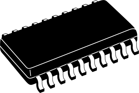
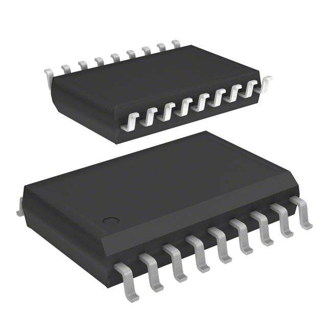
| 描述 | IC RTC CLK/CALENDAR SPI 20-SOIC |
| 产品分类 | |
| 品牌 | Intersil |
| 数据手册 | |
| 产品图片 |
|
| 产品型号 | CDP68HC68T1MZ |
| rohs | 无铅 / 符合限制有害物质指令(RoHS)规范要求 |
| 产品系列 | - |
| 供应商器件封装 | 20-SOIC W |
| 包装 | 管件 |
| 存储容量 | 32B |
| 安装类型 | 表面贴装 |
| 封装/外壳 | 20-SOIC(0.295",7.50mm 宽) |
| 工作温度 | -40°C ~ 85°C |
| 接口 | SPI |
| 日期格式 | YY-MM-DD-dd |
| 时间格式 | HH:MM:SS(12/24 小时) |
| 标准包装 | 38 |
| 特性 | 警报器,闰年,方波输出,监视计时器 |
| 电压-电源 | 3 V ~ 6 V |
| 电压-电源,电池 | 2.2 V ~ 6 V |
| 电流-计时(最大) | 20µA ~ 500µA @ 5V |
| 类型 | 时钟/日历 |


- 商务部:美国ITC正式对集成电路等产品启动337调查
- 曝三星4nm工艺存在良率问题 高通将骁龙8 Gen1或转产台积电
- 太阳诱电将投资9.5亿元在常州建新厂生产MLCC 预计2023年完工
- 英特尔发布欧洲新工厂建设计划 深化IDM 2.0 战略
- 台积电先进制程称霸业界 有大客户加持明年业绩稳了
- 达到5530亿美元!SIA预计今年全球半导体销售额将创下新高
- 英特尔拟将自动驾驶子公司Mobileye上市 估值或超500亿美元
- 三星加码芯片和SET,合并消费电子和移动部门,撤换高东真等 CEO
- 三星电子宣布重大人事变动 还合并消费电子和移动部门
- 海关总署:前11个月进口集成电路产品价值2.52万亿元 增长14.8%


PDF Datasheet 数据手册内容提取
DATASHEET CDP68HC68T1 FN1547 CMOS Serial Real-Time Clock With RAM and Power Sense/Control Rev 9.00 Decemember 8, 2015 The CDP68HC68T1 Real-Time Clock provides a Features time/calendar function, a 32 byte static RAM, and a 3 wire • SPI (Serial Peripheral Interface) Serial Peripheral Interface (SPI Bus). The primary function of the clock is to divide down a frequency input that can be • Full Clock Features supplied by the on-board oscillator in conjunction with an - Seconds, Minutes, Hours (12/24, AM/PM), Day of external crystal or by an external clock source. The internal Week, Date, Month, Year (0 to 99), Automatic Leap Year oscillator can operate with a 32kHz, 1MHz, 2MHz, or 4MHz • 32 Wordx8-Bit RAM crystal. An external clock source with a 32kHz, 1MHz, 2MHz, • Seconds, Minutes, Hours Alarm 4MHz, 50Hz or 60Hz frequency can be used to drive the CDP68HC68T1. The time registers hold seconds, minutes, • Automatic Power Loss Detection and hours, while the calendar registers hold day-of-week, • Low Minimum Standby (Timekeeping) Voltage . . . . . 2.2V date, month, and year information. The data is stored in BCD format. In addition, 12 or 24 hour operation can be selected. • Selectable Crystal or 50/60Hz Line Input In 12 hour mode, an AM/PM indicator is provided. The T1 • Buffered Clock Output has a programmable output which can provide one of seven • Battery Input Pin that Powers Oscillator and also outputs for use elsewhere in the system. Connects to VDD Pin When Power Fails Computer handshaking is controlled with a “wired-OR” interrupt • Three Independent Interrupt Modes output. The interrupt can be programmed to provide a signal as - Alarm the result of: - Periodic 1. An alarm programmed to occur at a predetermined - Power-Down Sense combination of seconds, minutes, and hours. • Pb-Free Available (RoHS Compliant) 2. One of 15 periodic interrupts ranging from sub-second to once per day frequency. 3. A power fail detect. The PSE output and the VSYS input are used for external power control. The CPUR output is available to reset the processor under power-down conditions. CPUR is enabled under software control and can also be activated via the CDP68HC68T1’s watchdog. If enabled, the watchdog requires a periodic toggle of the CE pin without a serial transfer. Pinouts CDP68HC68T1 CDP68HC68T1 (16 LD PDIP, SOIC) (20 LD SOIC) TOP VIEW TOP VIEW CLKOUT 1 16 VDD CLK OUT 1 20 VDD CPUR 2 15 XTAL OUT CPUR 2 19 XTAL OUT INT 3 14 XTAL IN INT 3 18 XTAL IN SCK 4 13 VBATT NC 4 17 NC MOSI 5 12 VSYS SCK 5 16 VBATT MISO 6 11 LINE MOSI 6 15 VSYS CE 7 10 POR MISO 7 14 NC VSS 8 9 PSE CE 8 13 NC VSS 9 12 LINE PSE 10 11 POR FN1547 Rev 9.00 Page 1 of 24 Decemember 8, 2015
CDP68HC68T1 Ordering Information PART NUMBER PART MARKING TEMP RANGE (°C) PACKAGE PKG DWG. # CDP68HC68T1E CDP68HC68T1E -40 to +85 16 Ld PDIP E16.3 (No longer available,recommended replacement: CDP68HC68T1EZ) CDP68HC68T1EZ (Note) CDP68HC68T1EZ -40 to +85 16 Ld PDIP** E16.3 (Pb-free) CDP68HC68T1M* 68HC68T1M -40 to +85 20 Ld SOIC M20.3 (No longer available,recommended Tape and Reel replacement: CDP68HC68T1MZ) CDP68HC68T1MZ* (Note) 68HC68T1MZ -40 to +85 20 Ld SOIC (Pb-free) M20.3 Tapeand Reel CDP68HC68T1M2* HC68T1M2 -40 to +85 16 Ld SOIC M16.3 (No longer available,recommended Tape and Reel replacement: CDP68HC68T1M2Z) CDP68HC68T1M2Z* (Note) HC68T1M2Z -40 to +85 16 Ld SOIC (Pb-free) M16.3 Tape and Reel *Add “96” suffix for tape and reel. Please refer to TB347 for details on reel specifications. **Pb-free PDIPs can be used for through hole wave solder processing only. They are not intended for use in Reflow solder processing applications. NOTE: These Intersil Pb-free plastic packaged products employ special Pb-free material sets; molding compounds/die attach materials and 100% matte tin plate PLUS ANNEAL - e3 termination finish, which is RoHS compliant and compatible with both SnPb and Pb-free soldering operations. Intersil Pb-free products are MSL classified at Pb-free peak reflow temperatures that meet or exceed the Pb-free requirements of IPC/JEDEC J STD-020. FN1547 Rev 9.00 Page 2 of 24 Decemember 8, 2015
CDP68HC68T1 Absolute Maximum Ratings Thermal Information Supply Voltage (VDD) . . . . . . . . . . . . . . . . . . . . . . . . . .-0.5V to +7V Thermal Resistance (Typical) JA (°C/W) JC (°C/W) Input Voltage (VIN). . . . . . . . . . . . . . . . . . . VSS -0.3V to VDD +0.3V 16 Ld PDIP* (Notes1, 3) . . . . . . . . . . . 85 35 Current Drain Per Input Pin (Excluding VDD and VSS I) . . . . . 10mA 16 Ld SOIC (Notes2, 3). . . . . . . . . . . . 65 26 Current Drain Per Output Pin I. . . . . . . . . . . . . . . . . . . . . . . . . 40mA 20 Ld SOIC (Notes2, 3). . . . . . . . . . . . 60 26 Maximum Junction Temperature (Plastic) . . . . . . . . . . . . . . .+150°C Operating Conditions Maximum Storage Temperature Range (TSTG). . . .-65°C to +150°C Pb-free Reflow Profile . . . . . . . . . . . . . . . . . . . . . . . . . . . see TB493 Voltage Range. . . . . . . . . . . . . . . . . . . . . . . . . . . . . .+3.0V to +6.0V *Pb-free PDIPs can be used for through hole wave solder processing Standby (Timekeeping) Voltage. . . . . . . . . . . . . . . . .+2.2V to +6.0V only. They are not intended for use in Reflow solder processing Temperature Range applications. CDP68HC68T1E (PDIP Package). . . . . . . . . . . . .-40°C to +85°C CDP68HC68T1M/M2 (SOIC Packages) . . . . . . . .-40°C to +85°C Input Voltage Input High. . . . . . . . . . . . . . . . . . . . . . . . . . . . .(0.7 x VDD) to VDD Input Low . . . . . . . . . . . . . . . . . . . . . . . . . . . . . .0V to (0.3 x VDD) Serial Clock Frequency (fSCK). . . . . . . . . . . . . . . . . .+3.0V to +6.0V CAUTION: Do not operate at or near the maximum ratings listed for extended periods of time. Exposure to such conditions may adversely impact product reliability and result in failures not covered by warranty. NOTES: 1. JA is measured with the component mounted on a low effective thermal conductivity test board in free air. See Tech Brief TB379 for details. 2. JA is measured with the component mounted on a high effective thermal conductivity test board in free air. See Tech Brief TB379 for details. 3. For JC, the “case temp” location is taken at the package top center. Static Electrical Specifications At TA = -40°C to +85°C, VDD = VBATT = 5V ±5%, Unless Otherwise Specified. CDP68HC68T1 TYP PARAMETER SYMBOL TEST CONDITIONS MIN (Note 4) MAX UNITS Quiescent Device Current IDD - 1 10 µA Output Voltage High Level VOH IOH = -1.6mA, VDD = 4.5V 3.7 - - V Output Voltage Low Level VOL IOL = 1.6mA, VDD = 4.5V - - 0.4 V Output Voltage High Level VOH IOH 10µA, VDD = 4.5V 4.4 - - V Output Voltage Low Level VOL IOL 10µA, VDD = 4.5V - - 0.1 V Input Leakage Current IIN - - ±1 µA Three-State Output Leakage Current IOUT - - ±10 µA Operating Current (Note 5) 32kHz - 0.08 - mA (ID + IB) VDD = VB = 5V 1MHz - 0.5 - mA Crystal Operation 2MHz - 0.7 - mA 4MHz - 1 - mA XTAL IN Clock (Squarewave) (Note 5) 32kHz - 0.02 0.024 mA (ID + IB) VDD = VS = 5V 1MHz - 0.1 0.12 mA 2MHz - 0.2 0.24 mA 4MHz - 0.4 0.5 mA Standby Current (Note 5) IB 32kHz - 20 - µA VS = 3V 1MHz - 200 - µA Crystal Operation 2MHz - 300 - µA 4MHz - 500 - µA FN1547 Rev 9.00 Page 3 of 24 Decemember 8, 2015
CDP68HC68T1 Static Electrical Specifications At TA = -40°C to +85°C, VDD = VBATT = 5V ±5%, Unless Otherwise Specified. (Continued) CDP68HC68T1 TYP PARAMETER SYMBOL TEST CONDITIONS MIN (Note 4) MAX UNITS Operating Current (Note 5) ID IB - mA VDD = 5V, VB = 3V 32kHz - 0.025 0.015 - mA Crystal Operation 1MHz - 0.08 0.15 - mA 2MHz - 0.15 0.25 - mA 4MHz - 0.3 0.4 - mA Standby Current (Note 5) IB 32kHz - 10 - µA VB = 2.2V Crystal Operation Input Capacitance CIN VIN = 0, TA = +25°C - - 2 pF Maximum Rise and Fall Times tr, tf - - 2 µs (Except XTAL Input and POR Pin 10) - - µs Input Voltage (Line Input Pin Only, Power Sense 0 10 12 V Mode) VSYS > VBVT - 1.0 - V (For VB Not Internally Connected to VDD) Power-On Reset (POR) Pulse Width 100 75 - ns NOTES: 4. Typical values are for TA = +25°C and nominal VDD. 5. Clock out (Pin 1) disabled, outputs open circuited. No serial access cycles. Dynamic Electrical Specifications Bus Timing VDD ±10%, VSS = 0VDC, TA = -40°C to +85°C LIMITS (ALL TYPES) VDD = 3.3V VDD = 5V IDENTIFICATION NUMBER PARAMETER SYMBOL MIN MAX MIN MAX UNITS 1 Chip Enable Setup Time tEVCV 200 - 100 - ns 2 Chip Enable After Clock Hold Time tCVEX 250 - 125 - ns 3 Clock Width High tWH 400 - 200 - ns 4 Clock Width Low tWL 400 - 200 - ns 5 Data In to Clock Setup Time tDVCV 200 - 100 - ns 7 Clock to Data Propagation Delay tCVDV - 200 - 100 ns 8 Chip Disable to Output High Z tEXQZ - 200 - 100 ns 11 Output Rise Time tr - 200 - 100 ns 12 Output Fall Time tf - 200 - 100 ns A Data in After Clock Hold Time tCVDX 200 - 100 - ns B Clock to Data Out Active tCVQX - 200 - 100 ns C Clock Recovery Time tREC 200 - 200 - ns FN1547 Rev 9.00 Page 4 of 24 Decemember 8, 2015
DF Functional Block Diagram C eN D cememb1547Re CE CFRIRECEUZIET AHMOU - RP MLO AGNIDC CALLOEGNIDCAR P68HC6 ev 8 r 8, 2 9.00 LINE 50/60Hz T1 0 1 XTAL IN 5 DAY/DAY XTAL OUT OSCILLATOR PRESCALE SECOND MINUTE HOUR OF WEEK MONTH VBATT PRESCALE CLOCK SELECT SELECT CLOCK OUT CLOCK CONTROL 8-BIT DATA BUS REGISTER INT CLOCK AND VDD INT INTERRUPT YEAR C VSS LOGIC RCEOGNITSRTOERL DP COMPARATOR 6 8 H SECOND MINUTE HOUR C LATCH LATCH LATCH 6 8 T LINE 1 VSYS POWER INT STATUS SENSE POR CONTROL REGISTER PSE 32x8 RAM CPUR SCK MISO MOSI SERIAL INTERFACE P a g e FIGURE 1. REAL TIME CLOCK FUNCTIONAL DIAGRAM 5 o f 2 4
CDP68HC68T1 0 $00 32 SECONDS R, W $20 33 MINUTES R, W $21 34 HOURS R, W $22 32 RAM LOCATIONS 35 DAY OF WEEK R, W $23 36 DATE R, W $24 37 MONTH R, W $25 31 $1F 38 YEARS R, W $26 32 $20 39 NOT USED $27 40 SEC ALARM W $28 CLOCK/CALENDAR 41 MIN ALARM W $29 50 $32 42 HRS ALARM W $2A 51 $33 43 NOT USED $2B 44 NOT USED $2C 45 NOT USED $2D 13 BYTES UNUSED 46 NOT USED $2E 47 NOT USED $2F 48 STATUS REGISTER R $30 63 $3F 49 CONTROL REGISTER R, W $31 85 TEST MODE $55 50 INTERRUPT CONTROL REGISTER R, W $32 R = READABLE W = WRITABLE FIGURE 2. ADDRESS MAP TABLE 1. CLOCK/CALENDAR AND ALARM DATA MODES BCD DATE EXAMPLE ADDRESS LOCATION (H) FUNCTION DECIMAL RANGE BCD DATA RANGE (Note 6) 20 Seconds 0 to 59 00 to 59 18 21 Minutes 0 to 59 00 to 59 49 22 Hours 1 to 12 81 to 92 (AM) A3 12 Hour Mode A1 to B2 (PM) (Note 7) Hours 0 to 23 00 to 23 15 24 Hour Mode 23 Day of the Week 1 to 7 01 to 07 03 (Sunday = 1) 24 Day of the Month 1 to 31 01 to 31 29 (Date) 25 Month 1 to 12 01 to 12 10 Jan = 1, Dec = 12 26 Years 0 to 99 00 to 99 85 28 Alarm Seconds 0 to 59 00 to 59 18 29 Alarm Minutes 0 to 59 00 to 59 49 2A Alarm Hours (Note 8) 1 to 12 01 to 12 (AM) 23 12 Hour Mode 21 to 32 (PM) Alarm Hours 0 to 23 00 to 23 15 24 Hour Mode NOTES: 6. Example: 3:49:18, Tuesday. Oct. 29,1985. 7. Most significant Bit, D7, is “0” for 24 hours, and “1” for 12 hour mode. Data Bit D5 is “1” for PM and ‘0” for AM in 12 hour mode. 8. Alarm hours. Data Bit D5 is “1” for PM and “0” for AM in 12 hour mode. Data Bits D7 and D6 are DON’T CARE. FN1547 Rev 9.00 Page 6 of 24 Decemember 8, 2015
CDP68HC68T1 Programmers Model - Clock Registers HEX ADDRESS WRITE/READ REGISTERS NAME DB7 DB0 TENS 0 TO 5 UNITS 0 TO 9 SECONDS (00 TO 59) 20 TENS 0 TO 5 UNITS 0 TO 9 MINUTES (00 TO 59) 21 12 DB7, 1 = 12 HR, 0 = 24 HR PM/AM HR X UNITS 0 TO 9 DB = 1 PM, 0 = AM TENS 0 TO 2 22 24 HOURS (01 TO 12 OR 00 TO 23 X X X X X UNITS 1 TO 7 DAY OF WK (01 TO 07) SUNDAY = 1 23 01 TO 28 DATE 29 TENS 0 TO 3 UNITS 0 TO 9 DAY OF MONTH 30 24 31 MONTH (01 TO 12) JAN = 1 TENS 0 TO 1 UNITS 0 TO 9 DEC = 12 25 TENS 0 TO 9 UNITS 0 TO 9 YEARS (00 TO 99) 26 7 6 5 4 3 2 1 0 CONTROL 31 7 6 5 4 3 2 1 0 INTERRUPT 32 WRITE ONLY REGISTERS TENS 0 TO 5 UNITS 0 TO 9 ALARM SECONDS (00 TO 59) 28 TENS 0 TO 5 UNITS 0 TO 9 ALARM MINUTES (00 TO 59) 29 ALARM HOURS (01 TO 12 OR 00 TO 23) X X PM/AM UNITS 0 TO 9 PLUS AM/PM IN 12 HR MODE 2A TENS 0 TO 2 PM = 1, AM = 0 READ ONLY REGISTERS 30 7 6 5 4 3 2 1 0 STATUS BIT 7 6 5 4 3 2 1 0 D7 D6 D5 D4 D3 D2 D1 D0 RAM DATA BYTE HEX ADDRESS 00-1F NOTE: X = Don’t care writes, X = 0 when read. FN1547 Rev 9.00 Page 7 of 24 Decemember 8, 2015
CDP68HC68T1 Functional Description years information. Data in the counters is in BCD format. The hours counter utilizes BCD for hour data plus bits for 12/24 hour The SPI real-time clock consists of a clock/calendar and a and AM/PM. The seven time counters are accessed serially at 32x8 RAM. Communications is established via the SPI addresses 20H through 26H. SeeTable1. (Serial Peripheral Interface) bus. In addition to the clock/calendar data from seconds to years, and system RAM flexibility provided by the 32-byte RAM, the clock features The real-time clock also has a static 32x8 RAM that is located computer handshaking with an interrupt output and a at addresses 00-1FH. Transmitting the address/control word separate squarewave clock output that can be one of seven with Bit 5 low selects RAM access. Bits 0 through 4 select the different frequencies. An alarm circuit is available that RAM location. compares the alarm latches with the seconds, minutes and Alarm hours time counters and activates the interrupt output when they are equal. The clock is specifically designed to aid in The alarm is set by accessing the three alarm latches and loading the required data. The alarm latches consist of power-down/power-up applications and offers several pins seconds, minutes and hours registers. When their outputs to aid the designer of battery backup systems. equal the values in the seconds, minutes and hours time Mode Select counters, an interrupt is generated. The interrupt output will go low if the alarm bit in the Interrupt Control Register is set high. The voltage level that is present at the VSYS input pin at the The alarm interrupt bit in the Status Register is set when the end of power-on-reset selects the device to be in the single interrupt occurs (see "Functional Description", INT Pin on supply or battery backup mode. page10). To preclude a false interrupt when loading the time Single-Supply Mode counters, the alarm interrupt bit should be set low in the Interrupt Control Register. This procedure is not required when If VSYS is a logic high when power-on-reset is completed, CLK the alarm time is set. OUT, PSE and CPUR will be enabled and the device will be completely operational. CPUR will be placed low if the logic Watchdog Function (See Figure 6) level at the VSYS pin goes low. If the output signals CLK OUT, When Bit 7 in the Interrupt Control Register is set high, the PSE and CPUR are disabled due to a power-down instruction, Clock’s CE (chip enable) pin must be toggled at a regular VSYS brought to a logic low and then to a logic high will re- interval without a serial data transfer. If the CE is not toggled, enable these outputs. An example of the single-supply mode is the clock will supply a CPU reset pulse and Bit 6 in the Status Register will be set. Typical service and reset times are listed in where only one supply is available and VDD, VBATT and VSYS Table 2. are tied together to the supply. TABLE 2. Battery Backup Mode 50Hz 60Hz XTAL If VSYS is a logic low at the end of power-on-reset, CLK MIN MAX MIN MAX MIN MAX OUT, PSE and CPUR will be disabled (CLK OUT, PSE and CPUR low). This condition will be held until VSYS rises to a Service Time - 10ms - 8.3ms - 7.8ms threshold (about 1.0V) above VBATT. The outputs CLK OUT, Reset Time 20 40ms 16.7 33.3ms 15.6 31.3ms PSE and CPUR will then be enabled and the device will be Clock Out operational. If VSYS falls below a threshold above VBATT the outputs CLK OUT, PSE and CPUR will be disabled. An The value in the three least significant bits of the Clock Control example of battery backup operation occurs if VSYS is tied to Register selects one of seven possible output frequencies. VDD and VDD is not connected to a supply when a battery is (See “Clock Control Register” on page11). This squarewave signal is available at the CLK OUT pin. When power-down connected to the VBATT pin. (See "Functional Description", operation is initiated, the output is set low. VBATT for Battery Backup Operation on page11.) Control Registers and Status Registers Clock/Calendar (See Figures 1 and 2) The operation of the Real-Time Clock is controlled by the Clock The clock/calendar portion of this device consists of a long Control and Interrupt Control Registers. Both registers are string of counters that is toggled by a 1Hz input. The 1Hz Read-Write Registers. Another register, the Status Register, is input is generated by a prescaler driven by an on-board available to indicate the operating conditions. The Status oscillator that utilizes one of four possible external crystals or Register is a Read only Register. that can be driven by an external clock source. The 1Hz Power Control trigger to the counters can also be supplied by a 50Hz or 60Hz input source that is connected to the LINE input pin. Power control is composed of two operations, Power Sense and Power-Down/Power-Up. Two pins are involved in power The time counters offer seconds, minutes and hours data in sensing, the LINE input pin and the INT output pin. Two 12 hour or 24 hour format. An AM/PM indicator is available additional pins are utilized during power-down/power-up that once set, toggles every 12 hours. The calendar counters operation. They are the PSE (Power Supply Enable) output consist of day (day of week), date (day of month), month and pin and VSYS input pin. FN1547 Rev 9.00 Page 8 of 24 Decemember 8, 2015
CDP68HC68T1 XTAL IN INT INT XTAL OUT VDD 0V LINE CPU CDP68HC05C16B VDD REAL-TIME CLOCK CDP68HC68T1 I STATUS REGISTER FIGURE 3. POWER-SENSING FUNCTIONAL DIAGRAM FROM SYSTEM TO SYSTEM POWER POWER CONTROL POWER-UP PSE VSYS PSE POWER SENSE OR I ALARM CPUR INTERRUPT CLK OSC CIRCUIT CONTROL OUT CLK REGISTER OUT CPUR RESET PERIODIC INTERRUPT MISO SIGNAL SERIAL INT INTERFACE MOSI MISO SERIAL INTERFACE REAL-TIME CLOCK CPU MOSI CDP68HC68T1 CDP68HC05C4B REAL-TIME CLOCK CDP68HC68T1 FIGURE 4. POWER-DOWN FUNCTIONAL DIAGRAM FIGURE 5. POWER-UP FUNCTIONAL DIAGRAM (INITIATED BY INTERRUPT SIGNAL Power Sensing (See Figure 3) signal to present at the LINE input pin to setup the power When Power Sensing is enabled (Bit 5 = 1 in Interrupt sense function. Control Register), AC transitions are sensed at the LINE input Power-Down (See Figure 4) pin. Threshold detectors determine when transitions cease. Power-down is a processor-directed operation. A bit is set in After a delay of 2.68ms to 4.64ms, plus the external input the Interrupt Control Register to initiate operation. Three pins circuit RC time constant, an interrupt is generated and a bit is are affected. The PSE (Power Supply Enable) output, set in the Status Register. This bit can then be sampled to see normally high, is placed low. The CLK OUT is placed low. if system power has turned back on. See "Functional The CPUR output, connected to the processors reset input Description", Line pin on page10. The power-sense circuitry is also placed low. In addition, the Serial Interface is operates by sensing the level of the voltage presented at the disabled. line input pin. This voltage is centered around VDD and as long as it is either plus or minus a threshold (about 1V) from Power-Up (See Figures 5 and 6) VDD a power-sense failure will not be indicated. With an AC Two conditions will terminate the Power-Down mode. signal present, remaining in this VDD window longer than a minimum of 2.68ms will activate the power-sense circuit. The 1. The first condition (see Figure 5) requires an interrupt. The interrupt can be generated by the alarm circuit, the larger the amplitude of the AC signal, the less time it spends programmable periodic interrupt signal, or the power in the VDD window, and the less likely a power failure will be sense circuit. detected. A 60Hz, 10VP-P sinewave voltage is an applicable FN1547 Rev 9.00 Page 9 of 24 Decemember 8, 2015
CDP68HC68T1 2. The second condition that releases Power-Down occurs SCK, MOSI, MISO when the level on the VSYS pin rises about 1.0V above See “Serial Peripheral Interface (SPI)” on page8. the level at the VBATT input, after previously falling to the level of VBATT (see Figure 6) in the Battery Backup Mode CE or VSYS falls to logic low and returns high in the Single A positive chip-enable input. A low level at this input holds Supply Mode. the serial interface logic in a reset state. This pin is also used for the watchdog function. V SS VBATT The negative power-supply pin that is connected to ground. VSYS PSE PSE CPUR Power-supply enable output pin. This pin is used to control power to the system. The pin is set high when: CLK OUT 1. VSYS rises above the VBATT voltage after VSYS was MISO placed low by a system failure. SERIAL INTERFACE 2. An interrupt occurs. MOSI REAL-TIME CLOCK 3. A power-on reset (if VSYS is a logic high). CDP68HC68T1 The PSE pin is set low by writing a high into bit 6 (power-down bit) in the Interrupt Control Register. FIGURE 6. POWER-UP FUNCTIONAL DIAGRAM (INITIATED BY A RISE IN VOLTAGE ON THE “VSYS” PIN) POR CLK OUT Power-on reset. A Schmitt-trigger input that generates a Clock output pin. One of seven frequencies can be selected power-on internal reset signal using an external RC (or this output can be set low) by the levels of the three network. Both control registers and frequency dividers for LSB’s in the Clock-Control Register. If a frequency is the oscillator and line input are reset. The Status Register selected, it will toggle with a 50% duty cycle except 2Hz in is reset except for the first time up bit (B4), which is set. the 50Hz time base mode. (e.g. if 1Hz is selected, the output Single supply or battery backup operation is selected at the will be high for 500ms and low for the same period). During end of POR. power-down operation (Bit 6 in Interrupt Control Register is LINE set to “1”), the clock-output pin will be set low. This input is used for two functions. When not used it CPUR should be connected to VDD via a 10k resistor. The first CPU reset output pin. This pin functions as an N-Channel function utilizes the input signal as the frequency source for only, open-drain output and requires an external pull-up the timekeeping counters. This function is selected by resistor. setting Bit 6 in the Clock Control Register. The second function enables the line input to sense a power failure. INT Threshold detectors operating above and below VDD sense Interrupt output pin. This output is driven from a single NFET an AC voltage loss. Bit 5 must be set to “1” in the Interrupt pulldown transistor and must be tied to an external pull-up Control Register and crystal or external clock source resistor. The output is activated to a low level when: operation is required. Bit 6 in the Clock Control Register must be low to select XTAL operation. 1. Power-sense operation is selected (B5 = 1 in Interrupt Control Register) and a power failure occurs. Oscillator Circuit 2. A previously set alarm time occurs. The alarm bit in the The CDP68HC68T1 has an on-board 150k resistor that is Status Register and interrupt-out signal are delayed switched in series with its internal inverter when 32kHz is 30.5µs when 32kHz operation is selected and 15.3µs for selected via the Clock Control Register. Note: When first 2MHz and 7.6µs for 4MHz. powered up the series resistor is not part of the oscillator 3. A previously selected periodic interrupt signal activates. circuit. (The CDP68HC68T1 sets up for a 4MHz oscillator). The Status Register must be read to set the Interrupt output high after the selected periodic interval occurs. This is also true when conditions 1 and 2 activate the interrupt. If power-down had been previously selected, the interrupt will also reset the power-down functions. FN1547 Rev 9.00 Page 10 of 24 Decemember 8, 2015
CDP68HC68T1 Line-XTAL 5pF TO 30pF XTAL When this bit is set high, clock operation will use the IN 8) L C1 50-cycle or 60-cycle input present at the LINE input pin. T1 22M NOTE RYSTA Wtimhee nu pthdea tbei.t is low, the crystal input will generate the 1Hz R ( C XTAL XTAL Select OUT 10pF TO 40pF C2 One of 4 possible crystals is selected by value in these two bits: 0 = 4.194304MHz 2 = 1.048576MHz NOTES: 9. All frequencies recommended oscillator circuit. C1, C2 values 1 = 2.097152MHz 3 = 32,768Hz crystal dependent. 50Hz to 60Hz 10. R is used for 32KHz operation only. 100k to 300k range as specified by crystal manufacturer. 50Hz is selected as the line input frequency when this bit is FIGURE 7. OSCILLATOR CIRCUIT set high. A low will select 60Hz. The power-sense bit in the Interrupt Control Register must be set low for line frequency V operation. SYS This input is connected to the system voltage. After the CPU Clock Out initiates power down by setting Bit 6 in the Interrupt Control The three bits specify one of the 7 frequencies to be used as Register to “1”, the level on this pin will terminate power the squarewave clock output: down if it rises about 1.0V above the level at the VBATT input pin after previously falling below VBATT +1.0V. When 0 = XTAL 4 = Disable (low output) power-down is terminated, the PSE pin will return high and 1 = XTAL/2 5 = 1Hz the Clock Output will be enabled. The CPUR output pin will 2 = XTAL/4 6 = 2Hz also return high. The logic level present at this pin at the end 3 = XTAL/8 7 = 50Hz or 60Hz of POR determines the CDP68HC68T1’s operating mode. XTAL Operation = 64Hz V All bits are reset by a power-on reset. Therefore, the XTAL is BATT selected as the clock output at this time. The oscillator power source. The positive terminal of the battery should be connected to this pin. When the level on Interrupt Control Register the VSYS pin falls below VBATT +1.0V, the VBATT pin will be internally connected to the VDD pin. When the voltage on Watchdog VSYS rises a threshold above (1.0V) the voltage on VBATT, When this bit is set high, the watchdog operation will be the connection from VBATT to the VDD pin is opened. When enabled. This function requires the CPU to toggle the CE pin the “LINE” input is used as the frequency source, VBATT periodically without a serial-transfer requirement. In the may be tied to VDD or VSS. The “XTAL IN” pin must be at event this does not occur, a CPU reset will be issued. Status VSS if VBATT is at VSS. If VBATT is connected to VDD, the Register must be read before re-enabling watchdog. “XTAL IN” pin can be tied to VSS or VDD. Power-Down XTAL IN, XTAL OUT A high in this location will initiate a power down. A CPU reset These pins are connected to a 32,768Hz. 1.048576MHz, will occur, the CLK OUT and PSE output pins will be set low 2.097152MHz or 4.194304MHz crystal. If an external clock and the serial interface will be disabled. is used, it should be connected to “XTAL IN” with ‘XTAL OUT” left open. Power Sense V This bit is used to enable the line input pin to sense a power DD failure. It is set high for this function. When power sense is The positive power-supply pin. selected, the input to the 50Hz to 60Hz prescaler is Clock Control Register disconnected. Therefore, crystal operation is required when power sense is enabled. An interrupt is generated when a Start-Stop power failure is sensed and the power sense and Interrupt A high written into this bit will enable the counter stages of True bit in the Status Register are set. When power sense is the clock circuitry. A low will hold all bits reset in the divider activated, a “0” must be written to this location followed by a chain from 32Hz to 1Hz. A clock out selected by Bit 0, Bit 1 “1” to re-enable power sense. and Bit 2 will not be affected by the stop function except the 1Hz and 2Hz outputs. FN1547 Rev 9.00 Page 11 of 24 Decemember 8, 2015
CDP68HC68T1 Alarm Periodic Select The output of the alarm comparator is enabled when this bit The value in these 4 bits will select the frequency of the is set high. When a comparison occurs between the periodic output. (See Table 3). seconds, minutes and hours time and alarm counters, the interrupt output is activated. When loading the time counters, this bit should be set low to avoid a false interrupt. This is not required when loading the alarm counters. See "Functional Description", INT for explanation of alarm delay on page10. CLOCK CONTROL REGISTER (Write/Read) - Address 31H D7 D6 D5 D4 D3 D2 D1 D0 START LINE XTAL XTAL 50Hz CLK OUT CLK OUT CLK OUT SEL SEL STOP XTAL 1 0 60Hz 2 1 0 INTERRUPT CONTROL REGISTER (Write/Read) - Address 32H D7 D6 D5 D4 D3 D2 D1 D0 WATCHDOG POWER POWER ALARM PERIODIC SELECT DOWN SENSE NOTE: All bits are reset by power-on reset. TABLE 3. PERIODIC INTERRUPT OUTPUT FREQUENCY TIME BASE PERIODIC INTERRUPT D0 - D3 VALUE OUTPUT FREQUENCY XTAL LINE 0 Disable 1 2048Hz X 2 1024Hz X 3 512Hz X 4 256Hz X 5 128Hz X 6 64Hz X 50Hz or 60Hz X 7 32Hz X 8 16Hz X 9 8Hz X 10 4Hz X 11 2Hz X X 12 1Hz X X 13 Minute X X 14 Hour X X 15 Day X X FN1547 Rev 9.00 Page 12 of 24 Decemember 8, 2015
CDP68HC68T1 STATUS REGISTER (Read Only) - Address 30H D7 D6 D5 D4 D3 D2 D1 D0 0 WATCHDOG TEST FIRST INTERRUPT POWER ALARM CLOCK MODE TIME TRUE SENSE INTERRUPT INTERRUPT UP INTERRUPT TRUTH TABLE SIGNAL MODE CE SCK (Note 11) MOSI MISO DISABLE L INPUT DISABLED INPUT DISABLED HIGH Z RESET WRITE H CPOL = 1 DATA BIT LATCH HIGH Z CPOL = 0 READ H CPOL = 1 X NEXT DATA BIT SHIFTED OUT (Note 12) CPOL = 0 NOTES: 11. When interfacing to CDP68HC05 microcontrollers, serial clock phase bit, CPHA, must be set = 1 in the microcomputer’s Control Register. 12. MISO remains at a high Z until 8-bits of data are ready to be shifted out during a READ. It remains at a high Z during the entire WRITE cycle. Watchdog Pin Signal Description If this bit is set high, the watchdog circuit has detected a SCK (Serial Clock Input) (Note 13) CPU failure. This input causes serial data to be latched from the MOSI Test Mode input and shifted out on the MISO output. When this bit is set high, the device is in the TEST MODE. MOSI (Master Out/Slave In) (Note 13) First-time Up Data bytes are shifted in at this pin, most significant bit Power-on reset sets this bit high. This signifies that data in (MSB) first. the RAM and Clock is not valid and should be initialized. MISO (Master In/Slave Out) Interrupt True Data bytes are shifted out at this pin, most significant bit A high in this bit signifies that one of the three interrupts (MSB) first. (Power Sense, Alarm, and Clock) is valid. CE (Chip Enable) (Note 14) Power-sense Interrupt A positive chip-enable input. A low level at this input holds This bit set high signifies that the power-sense circuit has the serial interface logic in a reset state, and disables the generated an interrupt. output driver at the MISO pin. Alarm Interrupt NOTES: When the seconds, minutes and hours time and alarm 13. These inputs will retain their previous state if the line driving them goes into a High-Z state. counter are equal, this bit will be set high. Status Register 14. The CE input has as internal pull-down device, if the input is in a must be read before loading Interrupt Control Register for low state before going to High Z, the input can be left in a High Z. valid alarm indication after alarm activates. Clock Interrupt A periodic interrupt will set this bit high. All bits are reset by a power-on reset except the “FIRST- TIME UP” which is set. All bits except the power-sense bit are reset after a read of this register. FN1547 Rev 9.00 Page 13 of 24 Decemember 8, 2015
CDP68HC68T1 Functional Description Address and Data Format The Serial Peripheral Interface (SPI) utilized by the There are three types of serial transfer: CDP68HC68T1 is a serial synchronous bus for address and 1. Address Control - Figure 9. data transfers. The clock, which is generated by the 2. READ or WRITE Data - Figure 10. microcomputer is active only during address and data transfers. In systems using the CDP68HC05C4 or 3. Watchdog Reset (actually a non-transfer) Figure 11. CDP68HC05D2, the inactive clock polarity is determined by The Address/Control and Data bytes are shifted MSB first, the CPOL bit in the microcomputer’s Control Register. A Into the serial data input (MOSI) and out of the serial data unique feature of the CDP68HC68T1 is that it automatically output (MISO). determines the level of the inactive clock by sampling SCK Any transfer of data requires an Address/Control byte to when CE becomes active (see Figure 8). Input data (MOSI) specify a Write or Read operation and to select a Clock or is latched internally on the internal strobe edge and output RAM location, followed by one or more bytes of data. data (MISO) is shifted out on the shift edge, as defined by Figure 8. There is one clock for each data bit transferred Data is transferred out of MISO for a Read and into MOSI for (address, as well as data bits are transferred in groups of 8). a Write operation. Address/Control Byte - (see Figure 9) INTERNAL CE SHIFT STROBE It is always the first byte received after CE goes true. To CPOL = 1 transmit a new address, CE must first go false and then true again. Bit 5 is used to select between Clock and RAM SCK locations. CE INTERNAL SHIFT STROBE CPOL = 0 SCK MOSI MSB MSB -1 NOTE: “CPOL” is a bit that is set in the microcomputer’s Control Register. FIGURE 8. SERIAL RAM CLOCK (SCK) AS A FUNCTION OF MCU CLOCK POLARITY (CPOL) BIT 7 6 5 4 3 2 1 0 W/R 0 CLK RAM A4 A3 A2 A1 A0 04 A0 through A4 Selects 5-bit HEX Address of RAM or specifies Clock Register. Most Significant Address Bit. If equal to “1”, A0 through A4 selects a Clock Register. If equal to “0”, A0 through A4 5 CLK RAM selects one of 32 RAM locations. Must be set to ”0” when not in Test Mode 7W/R W/R = “1” 6 0 initiates one or more WRITE cycles.W/R = “0”, initiates one or more READ cycles. 7 W/R CE SCK (NOTE) CLOCK MOSI W/R 0 A4 A3 A2 A1 A0 RAM NOTE: SCK can be either polarity. FIGURE 9. ADDRESS/CONTROL BYTE-TRANSFER WAVEFORMS FN1547 Rev 9.00 Page 14 of 24 Decemember 8, 2015
CDP68HC68T1 Read/Write Data (See Figure 10) Read/Write data follows the Address/Control byte. BIT 7 6 5 4 3 2 1 0 D7 D6 D5 D4 D3 D2 D1 D0 CE SCK (NOTE) MOSI D7 D6 D5 D4 D3 D2 D1 D0 MISO D7 D6 D5 D4 D3 D2 D1 D0 NOTE: SCK can be either polarity. FIGURE 10. READ/WRITE DATA TRANSFER WAVEFORMS Watchdog Reset (See Figure 11) Address and Data When watchdog operation is selected, CE must be toggled Data transfers can occur one byte at a time (Figure 12) or in periodically or a CPU reset will be outputted. a multibyte burst mode (Figure 13). After the Real-Time Clock enabled, an Address/Control word is sent to set the SERVICE SERVICE CLOCK or RAM and select the type of operation (i.e., Read TIME TIME or Write). For a single-byte Read or Write, one byte is CE transferred to or from the Clock Register or RAM location specified in the Address/Control byte and the Real-Time SCK Clock is then disabled. Write cycle causes the latched Clock CPUR Register or RAM address to automatically increment. Incrementing continues after each transfer until the device is FIGURE 11. WATCHDOG OPERATION WAVEFORMS disabled. After incrementing to 1FH the address will “wrap” to 00H and continue. Therefore, when the RAM is selected the address will “wrap” to 00H and when the clock is selected the address will “wrap” 20H. FN1547 Rev 9.00 Page 15 of 24 Decemember 8, 2015
CDP68HC68T1 CE SCK WRITE MOSI ADDRESS BYTE WRITE DATA MOSI ADDRESS BYTE READ MISO READ DATA FIGURE 12. SINGLE-BYTE TRANSFER WAVEFORMS CE SCK WRITE MOSI ADDRESS BYTE DATA BYTE DATA BYTE DATA BYTE MOSI ADDRESS BYTE READ MISO DATA BYTE DATA BYTE DATA BYTE DATA BYTE W/R ADDRESS DATA BYTE +1 DATA BYTE + (n-1) FIGURE 13. MULTIPLE-BYTE TRANSFER WAVEFORMS FN1547 Rev 9.00 Page 16 of 24 Decemember 8, 2015
CDP68HC68T1 Timing Diagrams 5 A 5 MOSI W/R A6 A0 D7O D6O D1N DON CE I C 2 SCK 4 3 FIGURE 14. WRITE-CYCLE TIMING WAVEFORMS 5 A MOSI W/R A6 A0 8 11 12 MISO D7O D6O DIN DON 7 8 CE I C 2 SCK 4 3 FIGURE 15. READ-CYCLE TIMING WAVEFORMS System Diagrams AC BRIDGE LINE REGULATOR VDDPOR VDD INT IRQ VSYS LINE VDD CDP68HC68T1 CDP68HC05C8B VBATT CPUR RESET CE PORT SCK SCK MOSI MOSI MISO MISO XTAL IN NOTE: Example of a system in which power is always on. Clock circuit driven by line input frequency. FIGURE 16. POWER-ON ALWAYS SYSTEM DIAGRAM FN1547 Rev 9.00 Page 17 of 24 Decemember 8, 2015
CDP68HC68T1 System Diagrams (Continued) BRIDGE AC GENERATOR LINE VBATT VDD VDD POR VSYS INT IRQ VDD CDP68HC68T1 CDP68HC05C8B LINE CPUR RESET CLK OUT OSC 1 CE PORT (e.g., PCO) MISO MISO VDD MOSI MOSI SCK SCK NOTE: Example of a system in which the power is controlled by an external source. The LINE input pin can sense when the switch opens by use of the POWER-SENSE INTERRUPT. The CDP68HC68T1 crystal drives the clock input to the CPU using the CLK OUT pin. On power down when VSYS < VBATT + 1.0V. VBATT will power the CDP68HC68T1. A threshold detect activates a P-Channel switch, connecting VBATT to VDD. VBATT always supplies power to the oscillator, keeping voltage frequency variation to a minimum. FIGURE 17. EXTERNALLY CONTROLLED POWER SYSTEM DIAGRAM A Procedure for Power-Down Operation might consist of the following: 1. Set power sense operation by writing Bit 5 high in the Interrupt Control Register. 2. When an interrupt occurs, the CPU reads the Status Register to determine the interrupt source. 3. Sensing a power failure, the CPU does the necessary housekeeping to prepare for shutdown. 4. The CPU reads the Status Register again after several milliseconds to determine validity of power failure. 5. The CPU sets power-down Bit 6 and disables all interrupts in the Interrupt Control Register when power down is verified. This causes the CPU reset and clock out to be held low and disconnects the serial interface. 6. When power returns and VSYS rises above VBATT, power-down is terminated. The CPU reset is released and serial communication is established. FN1547 Rev 9.00 Page 18 of 24 Decemember 8, 2015
CDP68HC68T1 System Diagrams (Continued) (EPS) AC ENABLED LINE REGULATOR POWER SUPPLY NC 0.1 R CHARGE 100k 0.047 POR VDD VSYS VDD VBATT 1k PSE M XTAL 22 CPUR RESET VDD CDP68HC05C4B LINE INT IRQ CLK 20k OUT OSC1 CE PORT RTC VDD SPI SPI VSS 3 VSS FIGURE 18. EXAMPLE OF A SYSTEM WITH A BATTERY BACKUP FN1547 Rev 9.00 Page 19 of 24 Decemember 8, 2015
CDP68HC68T1 System Diagrams (Continued) CLOCK BUTTON ENABLED POWER IGNITION 5V REG + 12V - LINE VDD VSYS VDD VBATT POR PORT PSE XTAL 2MHz CPUR RESET T1 CDP68HC05C4B CLK OUT OSC1 INT IRQ SPI SPI 3 VSS CE PORT VSS Example of an automotive system. The VSYS and LINE inputs can be used to sense the ignition turning on and off. An external switch is included to activate the system without turning on the ignition. Also, the CMOS CPU is not powered down with the system VDD, but is held in a low power reset mode during power down. When restoring power the CDP68HC68T1 will enable the CLK OUT pin and set the PSE and CPUR high. Important Application Note: Those units with a code of 6PG have delayed alarm interrupts of 8.3ms regardless of CDP68HC68T1’s operating frequency. (See "Functional Description", INT on page10.) In addition, reading the Status Register before delayed alarm activates will disable alarm signal. FIGURE 19. AUTOMOTIVE SYSTEM DIAGRAM FN1547 Rev 9.00 Page 20 of 24 Decemember 8, 2015
CDP68HC68T1 Revision History The revision history provided is for informational purposes only and is believed to be accurate, but not warranted. Please go to the web to make sure that you have the latest revision. DATE REVISION CHANGE December 8, 2015 FN1547.9 Updated Ordering Information Table on page2. Page 3: Changed Theta JA values and added Theta JC values: 16ld PDIP Theta Ja from 90 to 85. Theta Jc 35 (Notes 1,3) 16ld SOIC Theta Ja from 100 to 65. Theta Jc 26 (Notes 2,3) 20ld SOIC Theta Ja from 95 to 60. Theta Jc 26 (Notes 2,3) Added Notes 2 and 3 Updated Pb-free Reflow Profile link Added Revision History and About Intersil sections. Updated POD M20.3 to latest revision. Changes: Top View: Corrected "7.50 BSC" to "7.60/7.40" (no change from rev 2; error was introduced in conversion) Changed "10.30 BSC" to "10.65/10.00" (no change from rev 2; error was introduced in conversion) Side View: Changed "12.80 BSC" to "13.00/12.60" (no change from rev 2; error was introduced in conversion) Changed "2.65 max" to "2.65/2.35" (no change from rev 2; error was introduced in conversion) Changed Note 1 from "ANSI Y14.5M-1982." to "ASME Y14.5M-1994" Updated to new POD format by moving dimensions from table onto drawing and adding land pattern About Intersil Intersil Corporation is a leading provider of innovative power management and precision analog solutions. The company's products address some of the largest markets within the industrial and infrastructure, mobile computing and high-end consumer markets. For the most updated datasheet, application notes, related documentation and related parts, please see the respective product information page found at www.intersil.com. You may report errors or suggestions for improving this datasheet by visiting www.intersil.com/ask. Reliability reports are also available from our website at www.intersil.com/support FN1547 Rev 9.00 Page 21 of 24 Decemember 8, 2015
CDP68HC68T1 Dual-In-Line Plastic Packages (PDIP) N E16.3 (JEDEC MS-001-BB ISSUE D) E1 16 LEAD DUAL-IN-LINE PLASTIC PACKAGE INDEX AREA 1 2 3 N/2 INCHES MILLIMETERS -B- SYMBOL MIN MAX MIN MAX NOTES -A- A - 0.210 - 5.33 4 D E A1 0.015 - 0.39 - 4 BASE PLANE -C- A2 A A2 0.115 0.195 2.93 4.95 - SEATING B 0.014 0.022 0.356 0.558 - PLANE L CL B1 0.045 0.070 1.15 1.77 8, 10 DB11 e D1 A1 eC eAC C 0.008 0.014 0.204 0.355 - B D 0.735 0.775 18.66 19.68 5 e B 0.010 (0.25) M C A B S D1 0.005 - 0.13 - 5 NOTES: E 0.300 0.325 7.62 8.25 6 1. Controlling Dimensions: INCH. In case of conflict between English and E1 0.240 0.280 6.10 7.11 5 Metric dimensions, the inch dimensions control. e 0.100 BSC 2.54 BSC - 2. Dimensioning and tolerancing per ANSI Y14.5M-1982. 3. Symbols are defined in the “MO Series Symbol List” in Section 2.2 of eA 0.300 BSC 7.62 BSC 6 Publication No. 95. eB - 0.430 - 10.92 7 4. Dimensions A, A1 and L are measured with the package seated in JE- L 0.115 0.150 2.93 3.81 4 DEC seating plane gauge GS-3. N 16 16 9 5. D, D1, and E1 dimensions do not include mold flash or protrusions. Mold flash or protrusions shall not exceed 0.010 inch (0.25mm). Rev. 0 12/93 6. E and eA are measured with the leads constrained to be perpendic- ular to datum -C- . 7. eB and eC are measured at the lead tips with the leads unconstrained. eC must be zero or greater. 8. B1 maximum dimensions do not include dambar protrusions. Dambar protrusions shall not exceed 0.010 inch (0.25mm). 9. N is the maximum number of terminal positions. 10. Corner leads (1, N, N/2 and N/2 + 1) for E8.3, E16.3, E18.3, E28.3, E42.6 will have a B1 dimension of 0.030 - 0.045 inch (0.76 - 1.14mm). FN1547 Rev 9.00 Page 22 of 24 Decemember 8, 2015
CDP68HC68T1 Small Outline Plastic Packages (SOIC) M16.3 (JEDEC MS-013-AA ISSUE C) N 16 LEAD WIDE BODY SMALL OUTLINE PLASTIC PACKAGE INDEX AREA H 0.25(0.010) M B M INCHES MILLIMETERS E SYMBOL MIN MAX MIN MAX NOTES -B- A 0.0926 0.1043 2.35 2.65 - 1 2 3 A1 0.0040 0.0118 0.10 0.30 - L B 0.013 0.0200 0.33 0.51 9 SEATING PLANE C 0.0091 0.0125 0.23 0.32 - -A- D 0.3977 0.4133 10.10 10.50 3 D A h x 45° E 0.2914 0.2992 7.40 7.60 4 -C- e 0.050 BSC 1.27 BSC - H 0.394 0.419 10.00 10.65 - e A1 C h 0.010 0.029 0.25 0.75 5 B 0.10(0.004) L 0.016 0.050 0.40 1.27 6 0.25(0.010) M C A M B S N 16 16 7 NOTES: 0° 8° 0° 8° - 1. Symbols are defined in the “MO Series Symbol List” in Section 2.2 of Rev. 1 6/05 Publication Number 95. 2. Dimensioning and tolerancing per ANSI Y14.5M-1982. 3. Dimension “D” does not include mold flash, protrusions or gate burrs. Mold flash, protrusion and gate burrs shall not exceed 0.15mm (0.006 inch) per side. 4. Dimension “E” does not include interlead flash or protrusions. Interlead flash and protrusions shall not exceed 0.25mm (0.010 inch) per side. 5. The chamfer on the body is optional. If it is not present, a visual index feature must be located within the crosshatched area. 6. “L” is the length of terminal for soldering to a substrate. 7. “N” is the number of terminal positions. 8. Terminal numbers are shown for reference only. 9. The lead width “B”, as measured 0.36mm (0.014 inch) or greater above the seating plane, shall not exceed a maximum value of 0.61mm (0.024 inch) 10. Controlling dimension: MILLIMETER. Converted inch dimensions are not necessarily exact. © Copyright Intersil Americas LLC 2002-2015. All Rights Reserved. All trademarks and registered trademarks are the property of their respective owners. For additional products, see www.intersil.com/en/products.html Intersil products are manufactured, assembled and tested utilizing ISO9001 quality systems as noted in the quality certifications found at www.intersil.com/en/support/qualandreliability.html Intersil products are sold by description only. Intersil may modify the circuit design and/or specifications of products at any time without notice, provided that such modification does not, in Intersil's sole judgment, affect the form, fit or function of the product. Accordingly, the reader is cautioned to verify that datasheets are current before placing orders. Information furnished by Intersil is believed to be accurate and reliable. However, no responsibility is assumed by Intersil or its subsidiaries for its use; nor for any infringements of patents or other rights of third parties which may result from its use. No license is granted by implication or otherwise under any patent or patent rights of Intersil or its subsidiaries. For information regarding Intersil Corporation and its products, see www.intersil.com FN1547 Rev 9.00 Page 23 of 24 Decemember 8, 2015
CDP68HC68T1 CDP68HC68T1 Package Outline Drawing M20.3 20 LEAD WIDE BODY SMALL OUTLINE PLASTIC PACKAGE (SOIC) Rev 3, 2/11 20 INDEX AREA 10.65 0.25 (0.10) M B M 10.00 7.60 3 7.40 1 2 3 TOP VIEW 2 SEATING PLANE 1132..0600 2.65 5 1.27 2.35 0.40 0.75 x 45° 1.27 7 0.49 0.30 0.25 BSC 0.35 MAX 8° 0.25 (0.10) M C A M B S MAX 0.10 (0.004) 0.32 SIDE VIEW DETAIL "X" 0.23 NOTES: 1. Dimensioning and tolerancing per ASME Y14.5M-1994. (0.60) 1.27 BSC 2. Dimension does not include mold flash, protrusions or gate burrs. Mold flash, protrusion and gate burrs shall not exceed 20 0.15mm (0.006 inch) per side. (2.00) 3. Dimension does not include interlead lash or protrusions. Interlead flash and protrusions shall not exceed 0.25mm (0.010 inch) per side. 4. The chamfer on the body is optional. If it is not present, a visual index feature must be located within the crosshatched area. (9.40mm) 5. Dimension is the length of terminal for soldering to a substrate. 6. Terminal numbers are shown for reference only. 7. The lead width as measured 0.36mm (0.14 inch) or greater above the seating plane, shall not exceed a maximum value of 0.61mm (0.024 inch) 8. Controlling dimension: MILLIMETER. 1 2 3 9. Dimensions in ( ) for reference only. TYPICAL RECOMMENDED LAND PATTERN 10. JEDEC reference drawing number: MS-013-AC. FN1547 Rev 9.00 Page 24 of 24 Decemember 8, 2015