ICGOO在线商城 > 开发板,套件,编程器 > 评估和演示板和套件 > CDCE949PERF-EVM
 Datasheet下载
- 型号: CDCE949PERF-EVM
- 制造商: Texas Instruments
- 库位|库存: xxxx|xxxx
- 要求:
| 数量阶梯 | 香港交货 | 国内含税 |
| +xxxx | $xxxx | ¥xxxx |
查看当月历史价格
查看今年历史价格
CDCE949PERF-EVM产品简介:
ICGOO电子元器件商城为您提供CDCE949PERF-EVM由Texas Instruments设计生产,在icgoo商城现货销售,并且可以通过原厂、代理商等渠道进行代购。 CDCE949PERF-EVM价格参考¥1130.14-¥1130.14。Texas InstrumentsCDCE949PERF-EVM封装/规格:评估和演示板和套件, CDCE949PERF Clock Generator Timing Evaluation Board。您可以下载CDCE949PERF-EVM参考资料、Datasheet数据手册功能说明书,资料中有CDCE949PERF-EVM 详细功能的应用电路图电压和使用方法及教程。
Texas Instruments(德州仪器)的CDCE949PERF-EVM是一款评估模块,主要用于评估CDCE949高性能时钟发生器和 jitter cleaner 的性能。该器件适用于需要高精度、低抖动时钟信号的各种应用场景,以下是其主要的应用领域:

1. 通信基础设施
   - 用于基站、路由器、交换机和其他网络设备中,提供稳定的时钟源以支持高速数据传输和同步。
   - 支持多种通信标准(如以太网、光纤通道等),确保系统在复杂环境中保持低抖动和高可靠性。

2. 数据转换器时钟
   - 为模数转换器(ADC)和数模转换器(DAC)提供低相位噪声和低抖动的时钟信号,从而提升数据转换的精度和性能。
   - 广泛应用于音频处理、雷达系统和医疗成像等领域。

3. 测试与测量设备
   - 在示波器、频谱分析仪和信号发生器等精密测量设备中,提供高稳定性和低抖动的参考时钟。
   - 确保测量结果的准确性和一致性。

4. 工业自动化
   - 为工业控制和自动化系统中的实时数据采集和处理提供精确的时钟同步。
   - 支持多通道同步操作,提高系统的整体效率和可靠性。

5. 汽车电子
   - 在高级驾驶辅助系统(ADAS)、信息娱乐系统和车载网络中,提供可靠的时钟信号。
   - 满足汽车级应用对温度范围和抗干扰能力的严格要求。

6. 消费类电子产品
   - 用于高清电视、流媒体设备和游戏主机等,提供高质量的音视频同步时钟。
   - 改善用户体验,减少音频和视频失真。

CDCE949PERF-EVM通过灵活的配置选项和出色的性能表现,能够满足上述场景中对时钟信号的高精度需求,同时帮助设计工程师快速验证设计方案并加速产品开发进程。
| 参数 | 数值 |
| 产品目录 | 编程器,开发系统嵌入式解决方案 |
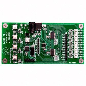
| 描述 | EVAL MOD PERFORMANCE FOR CDCE949时钟和定时器开发工具 Perf Eval Mod |
| 产品分类 | |
| 品牌 | Texas Instruments |
| 产品手册 | http://focus.ti.com/docs/toolsw/folders/print/cdce949perf-evm.html |
| 产品图片 |
|
| rohs | 否库存产品核实请求 / 库存产品核实请求 |
| 产品系列 | 模拟与数字IC开发工具,时钟和定时器开发工具,Texas Instruments CDCE949PERF-EVM- |
| 数据手册 | |
| 产品型号 | CDCE949PERF-EVM |
| 主要属性 | - |
| 主要用途 | 计时,时钟发生器 |
| 产品 | Evaluation Boards |
| 产品种类 | 时钟和定时器开发工具 |
| 使用的IC/零件 | CDCE949PERF |
| 其它名称 | 296-30832 |
| 制造商产品页 | http://www.ti.com/general/docs/suppproductinfo.tsp?distId=10&orderablePartNumber=CDCE949PERF-EVM |
| 商标 | Texas Instruments |
| 嵌入式 | - |
| 工作电源电压 | 1.8 V |
| 工作电源电流 | 2 mA |
| 工具用于评估 | CDCE949 |
| 工厂包装数量 | 1 |
| 所含物品 | 板 |
| 接口类型 | Serial |
| 标准包装 | 1 |
| 相关产品 | /product-detail/zh/CDCE949PW/296-21984-ND/1642942/product-detail/zh/CDCE949PWG4/CDCE949PWG4-ND/1897891/product-detail/zh/CDCE949PWR/CDCE949PWR-ND/1897892/product-detail/zh/CDCE949PWRG4/CDCE949PWRG4-ND/1897893 |
| 类型 | PLL Synthesizers / Multipliers / Dividers |
| 辅助属性 | - |
| 频率 | 230 MHz |


- 商务部:美国ITC正式对集成电路等产品启动337调查
- 曝三星4nm工艺存在良率问题 高通将骁龙8 Gen1或转产台积电
- 太阳诱电将投资9.5亿元在常州建新厂生产MLCC 预计2023年完工
- 英特尔发布欧洲新工厂建设计划 深化IDM 2.0 战略
- 台积电先进制程称霸业界 有大客户加持明年业绩稳了
- 达到5530亿美元!SIA预计今年全球半导体销售额将创下新高
- 英特尔拟将自动驾驶子公司Mobileye上市 估值或超500亿美元
- 三星加码芯片和SET,合并消费电子和移动部门,撤换高东真等 CEO
- 三星电子宣布重大人事变动 还合并消费电子和移动部门
- 海关总署:前11个月进口集成电路产品价值2.52万亿元 增长14.8%

PDF Datasheet 数据手册内容提取
Product Sample & Technical Tools & Support & Folder Buy Documents Software Community CDCE949,CDCEL949 SCAS844F–AUGUST2007–REVISEDOCTOBER2016 CDCE(L)913: Flexible Low Power LVCMOS Clock Generator With SSC Support for EMI Reduction 1 Features 2 Applications • MemberofProgrammableClockGenerator D-TVs, STBs, IP-STBs, DVD Players, DVD 1 Family Recorders,andPrinters – CDCEx913:1PLLs,3Outputs 3 Description – CDCEx925:2PLLs,5Outputs The CDCE949 and CDCEL949 are modular PLL- – CDCEx937:3PLLs,7Outputs based low cost, high-performance, programmable – CDCEx949:4PLLs,9Outputs clock synthesizers, multipliers and dividers. They generate up to 9 output clocks from a single input • In-SystemProgrammabilityandEEPROM frequency. Each output can be programmed in- – SerialProgrammableVolatileRegister system for any clock frequency up to 230 MHz, using – NonvolatileEEPROMtoStoreCustomer uptofourindependentconfigurablePLLs. Settings The CDCEx949 has separate output supply pins, • FlexibleInputClockingConcept V , 1.8 V for the CDCEL949, and 2.5 V to 3.3 V DDOUT – ExternalCrystal:8to32MHz forCDCE949. – On-ChipVCXO:Pull-Range ±150ppm The input accepts an external crystal or LVCMOS – Single-EndedLVCMOSUpto160MHz clock signal. If an external crystal is used, an on-chip load capacitor is adequate for most applications. The • FreeSelectableOutputFrequencyUpto230MHz value of the load capacitor is programmable from 0 to • Low-NoisePLLCore 20 pF. Additionally, an on-chip VCXO is selectable, – PLLLoopFilterComponentsIntegrated allowingsynchronizationoftheoutputfrequencytoan externalcontrolsignal,thatis,aPWMsignal. – LowPeriodJitter(Typical60ps) • SeparateOutputSupplyPins DeviceInformation(1) – CDCE949:3.3Vand2.5V PARTNUMBER PACKAGE BODYSIZE(NOM) – CDCEL949:1.8V CDCE949 TSSOP(24) 7.80mm×4.40mm • FlexibleClockDriver CDCEL949 – ThreeUser-DefinableControlInputs (1) For all available packages, see the orderable addendum at theendofthedatasheet. [S0/S1/S2],forExample,SSCSelection, FrequencySwitching,OutputEnableorPower TypicalApplicationSchematic Down – GeneratesHighlyAccurateClocksforVideo, Ethernet CDCE(L)9xx Audio,USB,IEEE1394,RFID, Bluetooth®, WiFi PHY Clock WLAN,Ethernet™,andGPS – GeneratesCommonClockFrequenciesUsed With TI-DaVinci™,OMAP™,DSPs 25 – ProgrammableSSCModulation USB MHz FPGA – Enables0-PPMClockGeneration Controller • 1.8-VDeviceCoreSupply • WideTemperatureRange:–40°Cto85°C Copyright © 2016, Texas Instruments Incorporated • PackagedinTSSOP • DevelopmentandProgrammingKitforEasyPLL DesignandProgramming(TIPro-Clock™) 1 An IMPORTANT NOTICE at the end of this data sheet addresses availability, warranty, changes, use in safety-critical applications, intellectualpropertymattersandotherimportantdisclaimers.PRODUCTIONDATA.
CDCE949,CDCEL949 SCAS844F–AUGUST2007–REVISEDOCTOBER2016 www.ti.com Table of Contents 1 Features.................................................................. 1 9.4 DeviceFunctionalModes........................................16 2 Applications........................................................... 1 9.5 Programming...........................................................17 3 Description............................................................. 1 9.6 RegisterMaps.........................................................18 4 RevisionHistory..................................................... 2 10 ApplicationandImplementation........................ 27 10.1 ApplicationInformation..........................................27 5 Description(continued)......................................... 4 10.2 TypicalApplication................................................27 6 PinConfigurationandFunctions......................... 4 11 PowerSupplyRecommendations..................... 31 7 Specifications......................................................... 5 12 Layout................................................................... 31 7.1 AbsoluteMaximumRatings......................................5 12.1 LayoutGuidelines.................................................31 7.2 ESDRatings..............................................................5 12.2 LayoutExample....................................................32 7.3 RecommendedOperatingConditions.......................6 13 DeviceandDocumentationSupport................. 33 7.4 ThermalInformation..................................................6 7.5 ElectricalCharacteristics...........................................7 13.1 DeviceSupport......................................................33 7.6 EEPROMSpecification.............................................8 13.2 RelatedDocumentation.........................................33 7.7 TimingRequirements:CLK_IN.................................9 13.3 RelatedLinks........................................................33 7.8 TimingRequirements:SDA/SCL..............................9 13.4 ReceivingNotificationofDocumentationUpdates33 7.9 TypicalCharacteristics............................................10 13.5 CommunityResources..........................................33 13.6 Trademarks...........................................................33 8 ParameterMeasurementInformation................11 13.7 ElectrostaticDischargeCaution............................34 9 DetailedDescription............................................ 12 13.8 Glossary................................................................34 9.1 Overview.................................................................12 14 Mechanical,Packaging,andOrderable 9.2 FunctionalBlockDiagram.......................................13 Information........................................................... 34 9.3 FeatureDescription.................................................13 4 Revision History NOTE:Pagenumbersforpreviousrevisionsmaydifferfrompagenumbersinthecurrentversion. ChangesfromRevisionE(August2016)toRevisionF Page • Changeddatasheettitlefrom:CDCEx949Programmable4-PLLVCXOClockSynthesizerWith1.8-V,2.5-V,and 3.3-VLVCMOSOutputsto:CDCE(L)913:FlexibleLowPowerLVCMOSClockGeneratorWithSSCSupportforEMI Reduction................................................................................................................................................................................ 1 ChangesfromRevisionD(March2010)toRevisionE Page • AddedDeviceInformationtable,ESDRatingstable,FeatureDescriptionsection,DeviceFunctionalModes, ApplicationandImplementationsection,PowerSupplyRecommendationssection,Layoutsection,Deviceand DocumentationSupportsection,andMechanical,Packaging,andOrderableInformationsection....................................... 1 • CondenseddownbulletsinFeatures..................................................................................................................................... 1 • Deleted'GeneralPurposeFrequencySynthesizing'fromApplications................................................................................. 1 • UpdatedvaluesintheThermalInformationtabletoalignwithJEDECstandards................................................................ 6 • ChangedByteReadProtocolimage,secondStoSr.......................................................................................................... 18 • Changed100MHz<ƒ >200MHz;TO80MHz≤ƒ ≤230MHz;andchanged0≤p≤7TO0≤p≤4...................29 VCO VCO • ChangedunderExample,fifthrow,N",2placesTON'....................................................................................................... 29 ChangesfromRevisionC(October2009)toRevisionD Page • AddedPLLsettingslimits:16≤q≤63,0≤p≤7,0≤r≤511,0<N<4096foottoPLL1,PLL2,PLL3,&PLL4 ConfigureRegisterTable...................................................................................................................................................... 22 2 SubmitDocumentationFeedback Copyright©2007–2016,TexasInstrumentsIncorporated ProductFolderLinks:CDCE949 CDCEL949
CDCE949,CDCEL949 www.ti.com SCAS844F–AUGUST2007–REVISEDOCTOBER2016 ChangesfromRevisionB(September2009)toRevisionC Page • Deletedsentence-Adifferentdefaultsettingcanbeprogrammedoncustomerrequest.ContactTexasInstruments salesormarketingrepresentativeformoreinformation....................................................................................................... 15 ChangesfromRevisionA(December2007)toRevisionB Page • AddedNote3:SDAandSCLcangoupto3.6VasstatedintheRecommendedOperatingConditionstable...................6 ChangesfromOriginal(August2007)toRevisionA Page • ChangedtheTHERMALRESISTANCEFORTSSOPtable.................................................................................................. 6 • ChangedGenericConfigurationRegistertableRIDFrom:0hTo:Xb................................................................................. 19 • AddednotetothePWDNdescription,GenericConfigurationRegistertable...................................................................... 19 Copyright©2007–2016,TexasInstrumentsIncorporated SubmitDocumentationFeedback 3 ProductFolderLinks:CDCE949 CDCEL949
CDCE949,CDCEL949 SCAS844F–AUGUST2007–REVISEDOCTOBER2016 www.ti.com 5 Description (continued) The deep M/N divider ratio allows the generation of zero-ppm audio or video, networking (WLAN, BlueTooth™, Ethernet, GPS) or Interface (USB, IEEE1394, Memory Stick) clocks from a reference input frequency, such as 27MHz. All PLLs support SSC (Spread-Spectrum Clocking). SSC can be Center-Spread or Down-Spread clocking. This isacommontechniquetoreduceelectro-magneticinterference(EMI). Based on the PLL frequency and the divider settings, the internal loop-filter components are automatically adjustedtoachievehighstability,andtooptimizethejitter-transfercharacteristicsofeachPLL. The device supports non-volatile EEPROM programming for easy customization of the device to the application. It is preset to a factory-default configuration. It can be reprogrammed to a different application configuration before PCB assembly, or reprogrammed by in-system programming. All device settings are programmable throughtheSDAandSCLbus,a2-wireserialinterface. Threeprogrammablecontrolinputs,S0,S1andS2,canbeusedtocontrolvariousaspectsofoperationincluding frequency selection, changing the SSC parameters to lower EMI, PLL bypass, power down, and choosing betweenlowlevelor3-statefortheoutput-disablefunction. TheCDCEx949operatesina1.8-Venvironment.Itoperateswithinatemperaturerangeof –40°Cto85°C. 6 Pin Configuration and Functions PWPackage 24-PinTSSOP (TopView) Xin/CLK 1 24 Xout S0 2 23 SDA/S1 VDD 3 22 SCL/S2 VCtrl 4 21 Y1 GND 5 20 GND VDDOUT 6 19 Y2 Y4 7 18 Y3 Y5 8 17 VDDOUT GND 9 16 Y6 VDDOUT 10 15 Y7 Y8 11 14 GND Y9 12 13 VDD Not to scale PinFunctions PIN TYPE(1) DESCRIPTION NAME NO. GND 5,9,14,20 G Ground SCL:Serialclockinput(defaultconfiguration),LVCMOS;internalpullup500kΩ;or SCL/S2 22 I S2:User-programmablecontrolinput;LVCMOSinputs;internalpullup500kΩ (1) G=Ground,I=Input,O=Output,P=Power 4 SubmitDocumentationFeedback Copyright©2007–2016,TexasInstrumentsIncorporated ProductFolderLinks:CDCE949 CDCEL949
CDCE949,CDCEL949 www.ti.com SCAS844F–AUGUST2007–REVISEDOCTOBER2016 PinFunctions(continued) PIN TYPE(1) DESCRIPTION NAME NO. SDA:Bidirectionalserialdatainput/output(defaultconfiguration),LVCMOS;internal SDA/S1 23 I/O pullup500kΩ;or S1:User-programmablecontrolinput;LVCMOSinputs;internalpullup500kΩ S0 2 I User-programmablecontrolinputS0;LVCMOSinputs;internalpullup500kΩ V 4 I VCXOcontrolvoltage(leaveopenorpullupwhennotused) Ctrl V 3,13 P 1.8-Vpowersupplyforthedevice DD CDCEL949:1.8-Vsupplyforalloutputs V 6,10,17 P DDOUT CDCE949:3.3-Vor2.5-Vsupplyforalloutputs Xin/CLK 1 I CrystaloscillatorinputorLVCMOSclockinput(selectablethroughSDA/SCLbus) Xout 24 O Crystaloscillatoroutput(leaveopenorpullupwhennotused) Y1 21 Y2 19 Y3 18 Y4 7 Y5 8 O LVCMOSoutput Y6 16 Y7 15 Y8 11 Y9 12 7 Specifications 7.1 Absolute Maximum Ratings overoperatingfree-airtemperaturerange(unlessotherwisenoted)(1) MIN MAX UNIT V Supplyvoltage –0.5 2.5 V DD V Inputvoltage(2) (3) –0.5 V +0.5 V I DD V Outputvoltage(2) –0.5 V +0.5 V O DDOUT I Inputcurrent(V <0,V >V ) 20 mA I I I DD I Continuousoutputcurrent 50 mA O T Junctiontemperature 125 °C J T Storagetemperature –65 150 °C stg (1) StressesbeyondthoselistedunderAbsoluteMaximumRatingsmaycausepermanentdamagetothedevice.Thesearestressratings onlyandfunctionaloperationofthedeviceattheseoranyotherconditionsbeyondthoseindicatedunderRecommendedOperating Conditionsisnotimplied.Exposuretoabsolute–maximum–ratedconditionsforextendedperiodsmayaffectdevicereliability. (2) Theinputandoutputnegativevoltageratingsmaybeexceedediftheinputandoutputclamp–currentratingsareobserved. (3) SDAandSCLcangoupto3.6VasstatedintheRecommendedOperatingConditionstable. 7.2 ESD Ratings VALUE UNIT Human-bodymodel(HBM),perANSI/ESDA/JEDECJS-001(1) ±2000 V Electrostaticdischarge V (ESD) Charged-devicemodel(CDM),perJEDECspecificationJESD22-C101(2) ±1500 (1) JEDECdocumentJEP155statesthat500-VHBMallowssafemanufacturingwithastandardESDcontrolprocess. (2) JEDECdocumentJEP157statesthat250-VCDMallowssafemanufacturingwithastandardESDcontrolprocess. Copyright©2007–2016,TexasInstrumentsIncorporated SubmitDocumentationFeedback 5 ProductFolderLinks:CDCE949 CDCEL949
CDCE949,CDCEL949 SCAS844F–AUGUST2007–REVISEDOCTOBER2016 www.ti.com 7.3 Recommended Operating Conditions MIN NOM MAX UNIT V Devicesupplyvoltage 1.7 1.8 1.9 V DD CDCE949 2.3 3.6 V OutputYxsupplyvoltage V DD(OUT) CDCEL949 1.7 1.9 V LowlevelinputvoltageLVCMOS 0.3×V V IL DD V HighlevelinputvoltageLVCMOS 0.7×V V IH DD V InputvoltagethresholdLVCMOS 0.5×V V I(thresh) DD S0 0 1.9 VIS Inputvoltage S1,S2,SDA,SCL, V 0 3.6 V =0.5×V Ithresh DD V InputvoltageCLK 0 1.9 V ICLK V =3.3V ±12 mA DDout I /I Outputcurrent V =2.5V ±10 mA OH OL DDout V =1.8V ±8 mA DDout C OutputloadLVCMOS 10 pF L T Operatingfree-airtemperature –40 85 °C A CRYSTALANDVCXO(1) f CrystalInputfrequency(fundamentalmode) 8 27 32 MHz Xtal ESR Effectiveseriesresistance 100 Ω f Pulling(0V≤V ≤1.8V)(2) ±120 ±150 ppm PR Ctrl V Frequencycontrolvoltage 0 V V (Ctrl) DD C /C Pullabilityratio 220 0 1 C On-chiploadcapacitanceatXinandXout 0 20 pF L (1) FormoreinformationaboutVCXOconfigurationandcrystalrecommendation,seeVCXOApplicationGuidelineforCDCE(L)9xxFamily (SCAA085). (2) Pullingrangedependsoncrystaltype,on-chipcrystalloadcapacitanceandPCBstraycapacitance;pullingrangeofmin±120ppm appliesforcrystallistedinVCXOApplicationGuidelineforCDCE(L)9xxFamily(SCAA085). 7.4 Thermal Information CDCEx949 THERMALMETRIC(1) PW(TSSOP) UNIT 24PINS Airflow0(LFM) 91 Airflow150(LFM) 75 θ Junction-to-ambientthermalresistance(2) Airflow200(LFM) 74 °C/W JA Airflow250(LFM) 73 Airflow500(LFM) 65 θ Junction-to-case(top)thermalresistance 0.5 °C/W JCtop θ Junction-to-boardthermalresistance 52 °C/W JB ψ Junction-to-topcharacterizationparameter 0.5 °C/W JT ψ Junction-to-boardcharacterizationparameter 50.1 °C/W JB θ Junction-to-case(bottom)thermalresistance 50 °C/W JCbot (1) Formoreinformationabouttraditionalandnewthermalmetrics,seetheSemiconductorandICPackageThermalMetricsapplication report. (2) ThepackagethermalimpedanceiscalculatedinaccordancewithJESD51andJEDEC2S2P(high-kboard). 6 SubmitDocumentationFeedback Copyright©2007–2016,TexasInstrumentsIncorporated ProductFolderLinks:CDCE949 CDCEL949
CDCE949,CDCEL949 www.ti.com SCAS844F–AUGUST2007–REVISEDOCTOBER2016 7.5 Electrical Characteristics overrecommendedoperatingfree-airtemperaturerange(unlessotherwisenoted) PARAMETER TESTCONDITIONS MIN TYP(1) MAX UNIT Alloutputsoff,f =27 AllPLLson 38 I Supplycurrent(seeFigure1) CLK mA DD MHz,fVCO=135MHz PerPLL 9 CDCE949 4 Supplycurrent Noload,alloutputson, VDDOUT=3.3V I mA DD(OUT) (seeFigure2andFigure3) fout=27MHz CDCEL949 2 V =1.8V DDOUT EverycircuitpowereddownexceptSDA/SCL, I Powerdowncurrent 50 µA DD(PD) f =0MHz,V =1.9V IN DD SupplyvoltageV threshold V DD 0.85 1.45 V (PUC) forpowerupcontrolcircuit f VCOfrequencyrangeofPLL 80 230 MHz VCO f LVCMOSoutputfrequency 230 MHz OUT LVCMOS V LVCMOSinputvoltage V =1.7V,I =–18mA –1.2 V IK DD I I LVCMOSinputcurrent V =0VorV ,V =1.9V ±5 µA I I DD DD LVCMOSinputcurrentfor I V =V ,V =1.9V 5 µA IH S0/S1/S2 I DD DD LVCMOSinputcurrentfor I V =0V,V =1.9V –4 µA IL S0/S1/S2 I DD InputcapacitanceatXin/Clk V =0VorV 6 ICLK DD InputcapacitanceatXout V =0VorV 2 C IXout DD pF I Inputcapacitanceat V =0VorV 3 S0/S1/S2 IS DD CDCE949–LVCMOSFORV =3.3V DDOUT V =3V,I =–0.1mA 2.9 DDOUT OH LVCMOShigh-leveloutput V V =3V,I =–8mA 2.4 V OH voltage DDOUT OH V =3V,I =–12mA 2.2 DDOUT OH V =3V,I =0.1mA 0.1 DDOUT OL LVCMOSlow-leveloutput V V =3V,I =8mA 0.5 V OL voltage DDOUT OL V =3V,I =12mA 0.8 DDOUT OL t , PLH Propagationdelay PLLbypass 3.2 ns t PHL t/t Riseandfalltime V =3.3V(20%–80%) 0.6 ns r f DDOUT 1PLLswitching,Y2-to-Y3 60 90 t Cycle-to-cyclejitter(2)(3) ps jit(cc) 4PLLsswitching,Y2-to-Y9 120 170 Peak-to-peakperiod 1PLLswitching,Y2-to-Y3 70 100 tjit(per) jitter(2)(3) 4PLLsswitching,Y2-to-Y9 130 180 ps f =50MHz,Y1-to-Y3 60 t Outputskew(4) OUT ps sk(o) f =50MHz,Y2-to-Y5orY6-to-Y9 160 OUT odc Outputdutycycle(5) f =100MHz,Pdiv=1 45% 55% VCO CDCE949–LVCMOSFORV =2.5V DDOUT V =2.3V,I =–0.1mA 2.2 DDOUT OH LVCMOShigh-leveloutput V V =2.3V,I =–6mA 1.7 V OH voltage DDOUT OH V =2.3V,I =–10mA 1.6 DDOUT OH (1) AlltypicalvaluesareatrespectivenominalV . DD (2) 10000cycles. (3) Jitterdependsondeviceconfiguration.Dataistakenunderthefollowingconditions:1-PLL:f =27MHz,Y2/3=27MHz,(measuredat IN Y2),4-PLL:f =27MHz,Y2/3=27MHz,(manuredatY2),Y4/5=16.384MHz,Y6/7=74.25MHz,Y8/9=48MHz. IN (4) Thet specificationisonlyvalidforequalloadingofeachbankofoutputsandoutputsaregeneratedfromthesamedivider;data sk(o) sampledonrisingedge(t). r (5) odcdependsonoutputrise-andfall-time(t/t). r f Copyright©2007–2016,TexasInstrumentsIncorporated SubmitDocumentationFeedback 7 ProductFolderLinks:CDCE949 CDCEL949
CDCE949,CDCEL949 SCAS844F–AUGUST2007–REVISEDOCTOBER2016 www.ti.com Electrical Characteristics (continued) overrecommendedoperatingfree-airtemperaturerange(unlessotherwisenoted) PARAMETER TESTCONDITIONS MIN TYP(1) MAX UNIT V =2.3V,I =0.1mA 0.1 DDOUT OL LVCMOSlow-leveloutput V V =2.3V,I =6mA 0.5 V OL voltage DDOUT OL V =2.3V,I =10mA 0.7 DDOUT OL t , PLH Propagationdelay PLLbypass 3.4 ns t PHL t/t Riseandfalltime V =2.5V(20%–80%) 0.8 ns r f DDOUT 1PLLswitching,Y2-to-Y3 60 90 ps t Cycle-to-cyclejitter(2)(3) jit(cc) 4PLLsswitching,Y2-to-Y9 120 170 Peak-to-peakperiod 1PLLswitching,Y2-to-Y3 70 100 ps tjit(per) jitter(2)(3) 4PLLsswitching,Y2-to-Y9 130 180 f =50MHz,Y1-to-Y3 60 t Outputskew(4) OUT ps sk(o) f =50MHz,Y2-to-Y5orY6-to-Y9 160 OUT odc Outputdutycycle(5) f =100MHz,Pdiv=1 45% 55% VCO CDCEL949–LVCMOSFORV =1.8V DDOUT V =1.7V,I =–0.1mA 1.6 DDOUT OH LVCMOShigh-leveloutput V V =1.7V,I =–4mA 1.4 V OH voltage DDOUT OH V =1.7V,I =–8mA 1.1 DDOUT OH V =1.7V,I =0.1mA 0.1 DDOUT OL LVCMOSlow-leveloutput V V =1.7V,I =4mA 0.3 V OL voltage DDOUT OL V =1.7V,I =8mA 0.6 DDOUT OL t , PLH Propagationdelay PLLbypass 2.6 ns t PHL t/t Riseandfalltime V =1.8V(20%–80%) 0.7 ns r f DDOUT 1PLLswitching,Y2-to-Y3 70 120 ps t Cycle-to-cyclejitter(2)(3) jit(cc) 4PLLsswitching,Y2-to-Y9 120 170 Peak-to-peakperiod 1PLLswitching,Y2-to-Y3 90 140 ps tjit(per) jitter(2)(3) 4PLLsswitching,Y2-to-Y9 130 190 f =50MHz,Y1-to-Y3 60 ps t Outputskew(4) OUT sk(o) f =50MHz,Y2-to-Y5orY6-to-Y9 160 OUT odc Outputdutycycle(5) f =100MHz,Pdiv=1 45% 55% VCO SDAANDSCL SCLandSDAinputclamp V V =1.7V,I =–18mA –1.2 V IK voltage DD I I SCLandSDAinputcurrent V =V ,V =1.9V ±10 µA IH I DD DD SDA/SCLinputhigh VIH voltage(6) 0.7×VDD V V SDA/SCLinputlowvoltage(6) 0.3×V V IL DD V SDAlow-leveloutputvoltage I =3mA,V =1.7V 0.2×V V OL OL DD DD C SCL/SDAinputcapacitance V =0VorV 3 10 pF I I DD (6) SDAandSCLpinsare3.3-Vtolerant. 7.6 EEPROM Specification MIN TYP MAX UNIT EEcyc ProgrammingcyclesofEEPROM 1000 cycles EEret Dataretention 10 years 8 SubmitDocumentationFeedback Copyright©2007–2016,TexasInstrumentsIncorporated ProductFolderLinks:CDCE949 CDCEL949
CDCE949,CDCEL949 www.ti.com SCAS844F–AUGUST2007–REVISEDOCTOBER2016 7.7 Timing Requirements: CLK_IN MIN NOM MAX UNIT PLLbypassmode 0 160 f LVCMOSclockinputfrequency MHz (CLK) PLLmode 8 160 t /t RiseandfalltimeCLKsignal(20%to80%) 3 ns r f duty DutycycleCLKatV /2 40% 60% CLK DD 7.8 Timing Requirements: SDA/SCL overoperatingfree-airtemperaturerange(unlessotherwisenoted;seeFigure14) MIN NOM MAX UNIT Standardmode 0 100 f SCLclockfrequency kHz (SCL) Fastmode 0 400 STARTsetuptime(SCLhighbefore Standardmode 4.7 t µs su(START) SDAlow) Fastmode 0.6 STARTholdtime(SCLlowafter Standardmode 4 t µs h(START) SDAlow) Fastmode 0.6 Standardmode 4.7 t SCLlow-pulseduration µs w(SCLL) Fastmode 1.3 Standardmode 4 t SCLhigh-pulseduration µs w(SCLH) Fastmode 0.6 SDAholdtime(SDAvalidafterSCL Standardmode 0 3.45 t µs h(SDA) low) Fastmode 0 0.9 Standardmode 250 t SDAsetuptime ns su(SDA) Fastmode 100 Standardmode 1000 t SCL/SDAinputrisetime ns r Fastmode 300 t SCL/SDAinputfalltime 300 ns f Standardmode 4 t STOPsetuptime µs su(STOP) Fastmode 0.6 BusfreetimebetweenaSTOPand Standardmode 4.7 t µs BUF STARTcondition Fastmode 1.3 Copyright©2007–2016,TexasInstrumentsIncorporated SubmitDocumentationFeedback 9 ProductFolderLinks:CDCE949 CDCEL949
CDCE949,CDCEL949 SCAS844F–AUGUST2007–REVISEDOCTOBER2016 www.ti.com 7.9 Typical Characteristics 100 35 90 VDD= 1.8 V VVDDDDO=U 1T.8= V3,.3 V, 9 outputs on 30 No Load 7 outputs on mA 80 4 PLLon 5 outputs on nt - 70 3 PLLon 25 3 outputs on e ply Curr 5600 1 PLL2o PnLLon - mAUT20 1 output on p O Su 40 all PLLoff DD15 all outputs off - I D ID 30 10 20 5 10 0 0 10 60 110 160 210 10 30 50 70 90 110 130150 170 190 210 230 PLL- Frequency - MHz fOUT- Output Frequency - MHz Figure1.CDCEx949SupplyCurrentvsPLLFrequency Figure2.CDCE949OutputCurrentvsOutputFrequency 12 VDD= 1.8 V, VDDOUT= 1.8 V, 9 outputs on 10 No Load 7 outputs on 5 outputs on 8 3 outputs on A m 1 output on - UT 6 O DD all outputs off I 4 2 0 10 30 50 70 90 110 130 150 170 190 210 230 fOUT- Output Frequency - MHz Figure3.CDCEL949OutputCurrentvsOutputFrequency 10 SubmitDocumentationFeedback Copyright©2007–2016,TexasInstrumentsIncorporated ProductFolderLinks:CDCE949 CDCEL949
CDCE949,CDCEL949 www.ti.com SCAS844F–AUGUST2007–REVISEDOCTOBER2016 8 Parameter Measurement Information Copyright © 2016,Texas Instruments Incorporated Figure4. TestLoad CDCE949 CDCEL949 LVCMOS LVCMOS Series Typical Driver Termination Line Impedance Impedance ~ 18 W Zo = 50W ~ 32W Copyright © 2016,Texas Instruments Incorporated Figure5. TestLoadfor50-ΩBoardEnvironment Copyright©2007–2016,TexasInstrumentsIncorporated SubmitDocumentationFeedback 11 ProductFolderLinks:CDCE949 CDCEL949
CDCE949,CDCEL949 SCAS844F–AUGUST2007–REVISEDOCTOBER2016 www.ti.com 9 Detailed Description 9.1 Overview The CDCE949 and CDCEL949 devices are modular PLL-based, low-cost, high-performance, programmable clock synthesizers, multipliers, and dividers. They generate up to nine output clocks from a single input frequency. Each output can be programmed in-system for any clock frequency up to 230 MHz, using one of the fourintegratedconfigurablePLLs. The CDCEx949 has separate output supply pins, V , which is 1.8 V for CDCEL949 and 2.5 V to 3.3 V for DDOUT CDCE949. The input accepts an external crystal or LVCMOS clock signal. If an external crystal is used, an on-chip load capacitor is adequate for most applications. The value of the load capacitor is programmable from 0 to 20 pF. Additionally, a selectable on-chip VCXO allows synchronization of the output frequency to an external control signal,thatis,thePWMsignal. The deep M/N divider ratio allows the generation of 0-ppm audio and video, networking (WLAN, Bluetooth, Ethernet, GPS), or Interface (USB, IEEE1394, memory stick) clocks from a reference input frequency such as 27MHz. All PLLs support spread-spectrum clocking (SSC). SSC can be center-spread or down-spread clocking. This is a commontechniquetoreduceelectro-magneticinterference(EMI). Based on the PLL frequency and the divider settings, the internal loop filter components are automatically adjustedtoachievehighstability,andtooptimizethejitter-transfercharacteristicsofeachPLL. The device supports non-volatile EEPROM programming for easy customization of the device to the application. It is preset to a factory-default configuration (see Default Device Setting). It can be reprogrammed to a different application configuration before PCB assembly, or reprogrammed by in-system programming. All device settings areprogrammablethroughtheSDAandSCLbus,a2-wireserialinterface. Threeprogrammablecontrolinputs,S0,S1andS2,canbeusedtocontrolvariousaspectsofoperationincluding frequency selection, changing the SSC parameters to lower EMI, PLL bypass, power down, and choosing betweenlowlevelor3-statefortheoutput-disablefunction. TheCDCEx949operatesina1.8-Venvironment.Itoperateswithinatemperaturerangeof –40°Cto85°C. 12 SubmitDocumentationFeedback Copyright©2007–2016,TexasInstrumentsIncorporated ProductFolderLinks:CDCE949 CDCEL949
CDCE949,CDCEL949 www.ti.com SCAS844F–AUGUST2007–REVISEDOCTOBER2016 9.2 Functional Block Diagram VDD GND VDDOUT Vctr Input Clock Xin/CLK M1 P1d0-iBvi1t CMLVOS Y1 VCXO XO LVCMOS PLL1 P7d-Bivit2 M2 CMLVOS Y2 Xout with SSC UX1 M EEPROM PLLBypass P7d-Bivit3 M3 CMLVOS Y3 Programming S0 and SS12//SSDCAL SRDeAg/iSstCerL PLL2 P7d-Bivit4 M4 CMLVOS Y4 with SSC X2 U M PLLBypass P7d-Bivit5 M5 CMLVOS Y5 PLL3 Pdiv6 M6 CMLVOS Y6 7-Bit with SSC X3 U M PLLBypass P7d-Bivit7 M7 CMLVOS Y7 PLL4 Pdiv8 M8 CMLVOS Y8 7-Bit with SSC X4 U M PLLBypass P7d-Bivit9 M9 CMLVOS Y9 Copyright © 2016,Texas Instruments Incorporated 9.3 Feature Description 9.3.1 ControlTerminalSetting The CDCEx949 has three user-definable control terminals (S0, S1, and S2) which allow external control of devicesettings.Theycanbeprogrammedtoanyofthefollowingsetting: • Spreadspectrumclockingselection→spreadtypeandspreadamountselection • Frequencyselection →switchingbetweenanyoftwouser-definedfrequencies • Outputstateselection→outputconfigurationandpowerdowncontrol Theusercanpredefineuptoeightdifferentcontrolsettings.Table1 andTable2explainthesesettings. Copyright©2007–2016,TexasInstrumentsIncorporated SubmitDocumentationFeedback 13 ProductFolderLinks:CDCE949 CDCEL949
CDCE949,CDCEL949 SCAS844F–AUGUST2007–REVISEDOCTOBER2016 www.ti.com Feature Description (continued) Table1.ControlTerminalDefinition EXTERNAL CONTROL PLL1SETTING PLL2SETTING PLL3SETTING PLL4SETTING Y1SETTING BITS n o cti e n n n n el o n o n o n o n S FCuonncttrioonl quencySelecti CSelection Y2/Y3Selectio quencySelecti CSelection Y4/Y5Selectio quencySelecti CSelection Y6/Y7Selectio quencySelecti CSelection Y8/Y9Selectio PowerDown Fre SS put Fre SS put Fre SS put Fre SS put and PLL Out PLL Out PLL Out PLL Out Y1 ut p ut O Table2.PLLxSetting(CanBeSelectedforEachPLLIndividual) SSCSELECTION(CENTER/DOWN)(1) SSCx[3-bits] CENTER DOWN 0 0 0 0%(off) 0%(off) 0 0 1 ±0.25% –0.25% 0 1 0 ±0.5% –0.5% 0 1 1 ±0.75% –0.75% 1 0 0 ±1% –1% 1 0 1 ±1.25% –1.25% 1 1 0 ±1.5% –1.5% 1 1 1 ±2% –2% FREQUENCYSELECTION(2) FSx FUNCTION 0 Frequency0 1 Frequency1 OUTPUTSELECTION(3)(Y2...Y9) YxYx FUNCTION 0 State0 1 State1 (1) Center/Down-Spread,Frequency0/1andState0/1areuser-definableinPLLxConfigurationRegister (2) Frequency0andFrequency1canbeanyfrequencywithinthespecifiedf range VCO (3) State0/1selectionisvalidforbothoutputsofthecorrespondingPLLmoduleandcanbepowerdown, 3-state,low,oractive Table3.Y1Setting(1) Y1SELECTION Y1 FUNCTION 0 State0 1 State1 (1) State0andState1areuserdefinableinGenericConfiguration Registerandcanbepowerdown,3-state,low,oractive. 14 SubmitDocumentationFeedback Copyright©2007–2016,TexasInstrumentsIncorporated ProductFolderLinks:CDCE949 CDCEL949
CDCE949,CDCEL949 www.ti.com SCAS844F–AUGUST2007–REVISEDOCTOBER2016 S1/SDA and S2/SCL pins of the CDCEx949 are dual function pins. In default configuration they are defined as SDA/SCL for the serial interface. They can be programmed as control-pins (S1/S2) by setting the relevant bits in the EEPROM. Note that the changes to the Control register (Bit [6] of Byte [02]) have no effect until they are writtenintotheEEPROM. Once they are set as control pins, the serial programming interface is no longer available. However, if V is DDOUT forcedtoGND,thetwocontrol-pins,S1andS2,temporallyactasserialprogrammingpins(SDA/SCL). S0isnotamulti-usepin,itisacontrolpinonly. 9.3.2 DefaultDeviceSetting The internal EEPROM of CDCEx949 is preconfigured as shown in Figure 6 (the input frequency is passed throughtotheoutputasadefault).Thisallowsthedevicetooperateindefaultmodewithouttheextraproduction step of program it. The default setting appears after power is supplied or after power-down or power-up sequence until it is re-programmed by the user to a different application configuration. A new register setting is programmedthroughtheserialSDA/SCLInterface. VDD GND Vddout Input Clock Xin M1 Pdiv1=1 CMLVOS Y1 = 27MHz 27MHz Crystal X-tal PLL1 Pdiv2 = 1 M2 CMLVOS Y2 = 27 MHz Xout power down MUX1 “1”=outputs enabled EEPROM PLLBypass Pdiv3 = 1 M3 CMLVOS Y3 = 27 MHz S0 Programming “0”= outputs 3-State and Programming Bus SSDCAL SRDeAg/iSstCeAr PLL2 Pdiv4 = 1 M4 CMLVOS Y4 = 27 MHz power down MUX2 PLLBypass Pdiv5 = 1 M5 CMLVOS Y5 = 27 MHz PLL3 Pdiv6 = 1 M6 CMLVOS Y6 = 27 MHz power down MUX3 PLLBypass Pdiv7 = 1 M7 CMLVOS Y7 = 27 MHz Figure6. DefaultDeviceSetting Table 4 shows the factory default setting for the Control Terminal Register (external control pins). In normal operation, all 8 register settings are available, but in the default configuration only the first two settings (0 and 1) canbeselectedwithS0,asS1andS2configuredasprogrammingpinsindefaultmode. Table4.FactoryDefaultSettingforControlTerminalRegister Y1 PLL1SETTING PLL2SETTING PLL3SETTING PLL3SETTING EXTERNAL OUTPUT FREQ. SSC OUTPUT FREQ. SSC OUTPUT FREQ. SSC OUTPUT FREQ. SSC OUTPUT CONTROLPINS(1) SELECT SELECT SEL. SELECT SELECT SEL. SELECT SELECT SEL. SELECT SELECT SEL. SELECT S2 S1 S0 Y1 FS1 SSC1 Y2Y3 FS2 SSC2 Y4Y5 FS3 SSC3 Y6Y7 FS4 SSC4 Y8Y9 SCL SDA (I2C) (I2C) 0 3-state fVCO1_0 off 3-state fVCO2_0 off 3-state fVCO3_0 off 3-state fVCO4_0 off 3-state SCL SDA (I2C) (I2C) 1 enabled fVCO1_0 off enabled fVCO2_0 off enabled fVCO3_0 off enabled fVCO4_0 off enabled (1) Indefaultmodeorwhenprogrammedrespectively,S1andS2actasserialprogramminginterface,SDA/SCL.Theydonothaveany control-pinfunctionbuttheyareinternallyinterpretedasifS1=0andS2=0.However,S0isacontrol-pinwhichinthedefaultmode switchesalloutputsONorOFF(aspreviouslypredefined). Copyright©2007–2016,TexasInstrumentsIncorporated SubmitDocumentationFeedback 15 ProductFolderLinks:CDCE949 CDCEL949
CDCE949,CDCEL949 SCAS844F–AUGUST2007–REVISEDOCTOBER2016 www.ti.com 9.3.3 SDA/SCLSerialInterface The CDCEx949 operates as a slave device of the 2-wire serial SDA/SCL bus, compatible with the popular SMBus or I2C Bus specification. It operates in the standard-mode transfer (up to 100 kbps) and fast-mode transfer(upto400kbps)andsupports7-bitaddressing. TheS1/SDAandS2/SCLpinsoftheCDCEx949aredualfunctionpins.Inthedefaultconfigurationtheyareused as SDA/SCL serial programming interface. They can be re-programmed as general-purpose control pins, S1 and S2,bychangingthecorrespondingEEPROMsetting,Byte02,Bit[6]. P S tw(SCLL) tBw(itS 7C L(HM)SB) Bit 6 Bit 0 (LSB) A P tr tf VIH SCL VIL tsu(START) th(START) tsu(SDA) th(SDA) tsu(STOP) t(BUS) tr tf VIH SDA VIL Figure7. TimingDiagramforSDA/SCLSerialControlInterface 9.3.4 DataProtocol ThedevicesupportsByteWriteandByteRead andBlockWriteandBlockRead operations. For ByteWrite/Read operations,thesystemcontrollercanindividuallyaccessaddressedbytes. For Block Write/Read operations, the bytes are accessed in sequential order from lowest to highest byte (with most significant bit first) with the ability to stop after any complete byte has been transferred. The numbers of Bytes read-out are defined by Byte Count in the Generic Configuration Register. At Block Read instruction all bytesdefinedintheByteCounthastobereadouttocorrectlyfinishthereadcycle. Once a byte has been sent, it is written into the internal register and is effective immediately. This applies to eachtransferredbyteindependentofwhetherthisisa ByteWriteoraBlockWritesequence. If the EEPROM Write Cycle is initiated, the internal SDA register contents are written into the EEPROM. During this write cycle, data is not accepted at the SDA/SCL bus until the write cycle is completed. However, data can be read during the programming sequence (Byte Read or Block Read). The programming status can be monitoredbyreadingEEPIP,Byte01–Bit[6]. Theoffsetoftheindexedbyteisencodedinthecommandcode,asdescribedinTable5. Table5.SlaveReceiverAddress(7Bits) DEVICE A6 A5 A4 A3 A2 A1(1) A0(1) R/W CDCEx913 1 1 0 0 1 0 1 1/0 CDCEx925 1 1 0 0 1 0 0 1/0 CDCEx937 1 1 0 1 1 0 1 1/0 CDCEx949 1 1 0 1 1 0 0 1/0 (1) AddressbitsA0andA1areprogrammablethroughtheSDA/SCLbus(Byte01,Bit[1:0]).Thisallowsaddressingupto4devices connectedtothesameSDA/SCLbus.Theleast-significantbitoftheaddressbytedesignatesawriteorreadoperation. 9.4 Device Functional Modes 9.4.1 SDA/SCLHardwareInterface Figure 8 shows how the CDCEx949 clock synthesizer is connected to the SDA/SCL serial interface bus. Multiple devices can be connected to the bus but the speed may need to be reduced (400 kHz is the maximum) if many devicesareconnected. 16 SubmitDocumentationFeedback Copyright©2007–2016,TexasInstrumentsIncorporated ProductFolderLinks:CDCE949 CDCEL949
CDCE949,CDCEL949 www.ti.com SCAS844F–AUGUST2007–REVISEDOCTOBER2016 Device Functional Modes (continued) Note that the pullup resistor value (R ) depends on the supply voltage, bus capacitance and number of P connected devices. The recommended pullup value is 4.7 kΩ. It must meet the minimum sink current of 3 mA at V =0.4Vfortheoutputstages(formoredetails,seeSMBus orI2CBusspecification). OLmax CDCE949 CDCEL949 RP RP Master Slave SDA SCL CBUS CBUS Copyright © 2016,Texas Instruments Incorporated Figure8. SDA/SCLHardwareInterface 9.5 Programming Table6.CommandCodeDefinition BIT DESCRIPTION 0=BlockReadorBlockWriteoperation 7 1=ByteReadorByteWriteoperation (6:0) ByteOffsetforByteRead,BlockRead,ByteWriteandBlockWriteoperation. 1 7 1 1 8 1 1 S SlaveAddress R/W A Data Byte A P MSB LSB MSB LSB S Start Condition Sr Repeated Start Condition R/W 1 = Read (Rd) from CDCE9xx device; 0 = Write (Wr) to the CDCE9xxx A Acknowledg (ACK = 0 and NACK =1) P Stop Condition Master to SlaveTransmission Slave to MasterTransmission Figure9. GenericProgrammingSequence 1 7 1 1 8 1 8 1 1 S SlaveAddress Wr A CommandCode A Data Byte A P Figure10. ByteWriteProtocol Copyright©2007–2016,TexasInstrumentsIncorporated SubmitDocumentationFeedback 17 ProductFolderLinks:CDCE949 CDCEL949
CDCE949,CDCEL949 SCAS844F–AUGUST2007–REVISEDOCTOBER2016 www.ti.com 1 7 1 1 8 1 1 7 1 1 S SlaveAddress Wr A CommandCode A Sr SlaveAddress Rd A 8 1 1 Data Byte A P Figure11. ByteReadProtocol 1 7 1 1 8 1 8 1 S SlaveAddress Wr A CommandCode A Byte Count = N A 8 1 8 1 8 1 1 Data Byte 0 A Data Byte 1 A … Data Byte N-1 A P NOTE: DataByte0Bits[7:0]isreservedforRevisionCodeandVendorIdentification.Alsoitisusedforinternaltestpurpose andmustnotbeoverwritten. Figure12. BlockWriteProgramming 1 7 1 1 8 1 1 7 1 1 S SlaveAddress Wr A CommandCode A Sr SlaveAddress Rd A 8 1 8 1 8 1 1 Byte Count N A Data Byte 0 A … Data Byte N-1 A P Figure13. BlockReadProtocol P S Bit 7 (MSB) Bit 6 Bit 0 (LSB) A P tw(SCLL) tw(SCLH) tr tf VIH SCL VIL tSU(START) th(START) tSU(SDA) th(SDA) tSU(STOP) t(BUS) tr tf VIH SDA VIL Figure14. TimingDiagramfortheSDA/SCLSerialControlInterface 9.6 Register Maps 9.6.1 SDA/SCLConfigurationRegisters The clock input, control pins, PLLs, and output stages are user configurable. The following tables and explanations describe the programmable functions of the CDCEx949. All settings can be manually written to the device through the SDA/SCL bus, or are easily programmable by using the TI Pro Clock software. TI Pro Clock software allows the user to quickly make all settings and automatically calculates the values for optimized performanceatlowestjitter. 18 SubmitDocumentationFeedback Copyright©2007–2016,TexasInstrumentsIncorporated ProductFolderLinks:CDCE949 CDCEL949
CDCE949,CDCEL949 www.ti.com SCAS844F–AUGUST2007–REVISEDOCTOBER2016 Table7.SDA/SCLRegisters ADDRESSOFFSET REGISTERDESCRIPTION TABLE 00h Genericconfigurationregister Table9 10h PLL1configurationregister Table10 20h PLL2configurationregister Table11 30h PLL3configurationregister Table12 40h PLL4configurationregister Table13 The grey-highlighted Bits described in the configuration registers tables on the following pages, belong to the Control Pin Register. The user can predefine up to eight different control settings. These settings can then be selectedbytheexternalcontrolpins,S0,S1,andS2(seeControlTerminalSetting). Table8.ConfigurationRegister,ExternalControlPins EXTERNAL Y1 PLL1SETTING PLL2SETTING PLL3SETTING PLL4SETTING CONTROL OUTPUT FREQ SSC OUTPUT FREQ SSC OUTPUT FREQ SSC OUTPUT FREQ SSC OUTPUT PINS SELECT SELECT SELECT SELECT SELECT SELECT SELECT SELECT SELECT SELECT SELECT SELECT SELECT S2 S1 S0 Y1 FS1 SSC1 Y2Y3 FS2 SSC2 Y4Y5 FS3 SSC3 Y6Y7 FS4 SSC4 Y8Y9 0 0 0 Y1_0 FS1_0 SSC1_0 Y2Y3_0 FS2_0 SSC2_0 Y4Y5_0 FS3_0 SSC3_0 Y6Y7_0 FS4_0 SSC4_0 Y8Y9_0 0 0 1 Y1_1 FS1_1 SSC1_1 Y2Y3_1 FS2_1 SSC2_1 Y4Y5_1 FS3_1 SSC3_1 Y6Y7_1 FS4_1 SSC4_1 Y8Y9_1 0 1 0 Y1_2 FS1_2 SSC1_2 Y2Y3_2 FS2_2 SSC2_2 Y4Y5_2 FS3_2 SSC3_2 Y6Y7_2 FS4_2 SSC4_2 Y8Y9_2 0 1 1 Y1_3 FS1_3 SSC1_3 Y2Y3_3 FS2_3 SSC2_3 Y4Y5_3 FS3_3 SSC3_3 Y6Y7_3 FS4_3 SSC4_3 Y8Y9_3 1 0 0 Y1_4 FS1_4 SSC1_4 Y2Y3_4 FS2_4 SSC2_4 Y4Y5_4 FS3_4 SSC3_4 Y6Y7_4 FS4_4 SSC4_4 Y8Y9_4 1 0 1 Y1_5 FS1_5 SSC1_5 Y2Y3_5 FS2_5 SSC2_5 Y4Y5_5 FS3_5 SSC3_5 Y6Y7_5 FS4_5 SSC4_5 Y8Y9_5 1 1 0 Y1_6 FS1_6 SSC1_6 Y2Y3_6 FS2_6 SSC2_6 Y4Y5_6 FS3_6 SSC3_6 Y6Y7_6 FS4_6 SSC4_6 Y8Y9_6 1 1 1 Y1_7 FS1_7 SSC1_7 Y2Y3_7 FS2_7 SSC2_7 Y4Y5_7 FS3_7 SSC3_7 Y6Y7_7 FS4_7 SSC4_7 Y8Y9_7 Addr. Offset(1) 04h 13h 10h-12h 15h 23h 20h-22h 25h 33h 30h-32h 35h 43h 40h-42h 45h (1) AddressOffsetreferstothebyteaddressintheConfigurationRegisteronfollowingpages. Table9.GenericConfigurationRegister OFFSET(1) BIT(2) ACRONYM DEFAULT(3) DESCRIPTION 00h 7 E_EL xb DeviceIdentification(readonly):‘1’isCDCE949(3.3V),‘0’isCDCEL949(1.8V) 6:4 RID Xb RevisionIdentificationNumber(readonly) 3:0 VID 1h VendorIdentificationNumber(readonly) 01h 7 – 0b Reserved-alwayswrite0 EEPROMProgramming 0–EEPROMprogrammingiscompleted 6 EEPIP 0b Status(4):(readonly) 1–EEPROMisinprogrammingmode PermanentlyLockEEPROM 0–EEPROMisnotlocked 5 EELOCK 0b Data(5): 1–EEPROMispermanentlylocked Devicepowerdown(overwritesS0/S1/S2setting;configurationregistersettingsareunchanged) Note:PWDNcannotbesetto1intheEEPROM. 4 PWDN 0b 0–deviceactive(allPLLsandalloutputsareenabled) 1–devicepowerdown(allPLLsinpowerdownandalloutputsin3-State) Inputclockselection: 00–X-tal 10–LVCMOS 3:2 INCLK 00b 01–VCXO 11–reserved 1:0 SLAVE_ADR 00b ProgrammableAddressBitsA0andA1oftheSlaveReceiverAddress (1) Writingdatabeyond50hmayadverselyaffectdevicefunction. (2) AlldataistransferredMSB-first. (3) Unlesscustomsettingisused. (4) DuringEEPROMprogramming,nodataisallowedtobesenttothedevicethroughtheSDA/SCLbusuntiltheprogrammingsequenceis completed.Data,however,canbereadduringtheprogrammingsequence(ByteReadorBlockRead). (5) IfthisbitissethighintheEEPROM,theactualdataintheEEPROMispermanentlylocked,andnofurtherprogrammingispossible. Data,howevercanstillbewrittenthroughtheSDA/SCLbustotheinternalregistertochangedevicefunctiononthefly.Butnewdata cannolongerbesavedtotheEEPROM.EELOCKiseffectiveonlyifwrittenintotheEEPROM Copyright©2007–2016,TexasInstrumentsIncorporated SubmitDocumentationFeedback 19 ProductFolderLinks:CDCE949 CDCEL949
CDCE949,CDCEL949 SCAS844F–AUGUST2007–REVISEDOCTOBER2016 www.ti.com Table9.GenericConfigurationRegister (continued) OFFSET(1) BIT(2) ACRONYM DEFAULT(3) DESCRIPTION 02h ClocksourceselectionforoutputY1: 0–inputclock 7 M1 1b 1–PLL1clock Operationmodeselectionforpin22/23(6) 6 SPICON 0b 0–serialprogramminginterfaceSDA(pin23)andSCL(pin22) 1–controlpinsS1(pin23)andS2(pin22) 5:4 Y1_ST1 11b Y1-State0/1Definition(appliestoY1_ST1andY1_ST0) 00–devicepowerdown(allPLLsinpowerdownandalloutputsin3-state) 01–Y1disabledto3-state 3:2 Y1_ST0 01b 10–Y1disabledtolow 11–Y1enabled(normaloperation) 1:0 Pdiv1[9:8] 10-BitY1-Output-Divider 0–dividerresetandstand-by 001h Pdiv1: 1-to-1023–dividervalue 03h 7:0 Pdiv1[7:0] 04h 7 Y1_7 0b Y1_xStateSelection(7) 6 Y1_6 0b 0–State0(predefinedbyY1-State0Definition[Y1_ST0]) 1–State1(predefinedbyY1-State1Definition[Y1_ST1]) 5 Y1_5 0b 4 Y1_4 0b 3 Y1_3 0b 2 Y1_2 0b 1 Y1_1 1b 0 Y1_0 0b 05h Crystalloadcapacitor 00h→0pF Vctr selection(8): 01h→1pF Xin 7:3 XCSEL 0Ah 02h→2pF i.e. 20pF VCXO 14h-to-1Fh→20pF XCSEL= 10pF XO Xout 20pF 2:0 — 0b Reserved-donotwriteothersthan0 06h 7-BitByteCount(DefinesthenumberofByteswhichissentfromthisdeviceatthenextBlockRead 7:1 BCOUNT 50h transfer;allbytesmustbereadouttocorrectlyfinishthereadcycle.) InitiateEEPROMWriteCycle(4)(9) 0 EEWRITE 0b 0–noEEPROMwritecycle 1–startEEPROMwritecycle(internalconfigurationregisterissavedtotheEEPROM) 07h-0Fh — — 0h Reserved–donotwriteothersthan0 (6) Selectionofcontrol-pinsiseffectiveonlyifwrittenintotheEEPROM.OncewrittenintotheEEPROM,theserialprogrammingpinsare nolongeravailable.However,ifV isforcedtoGND,thetwocontrol-pins,S1andS2,temporallyactasserialprogrammingpins DDOUT (SDA/SCL),andthetwoslavereceiveraddressbitsareresettoA0=0andA1=0. (7) ThesearethebitsoftheControlPinRegister.Theusercanpredefineuptoeightdifferentcontrolsettings.Thesesettingscanthenbe selectedbytheexternalcontrolpins,S0,S1,andS2. (8) Theinternalloadcapacitor(C ,C )mustbeusedtoachievethebestclockperformance.Externalcapacitorsmustbeusedonlytodoa 1 2 fineadjustmentofC byfewpF.ThevalueofC canbeprogrammedwitharesolutionof1pFforatotalcrystalloadrangeof0pFto20 L L pF.ForC >20pFuseadditionalexternalcapacitors.Also,thedeviceinputcapacitancemustbeconsidered;thisadds1.5pF(6pF,2 L pF)totheselectedC .FormoreinformationaboutVCXOconfigurationandcrystalrecommendations,seeVCXOApplicationGuideline L forCDCE(L)9xxFamily(SCAA085). (9) NOTE:TheEEPROMWRITEbitmustbesentlast.ThisensuresthatthecontentofallinternalregistersarewrittenintotheEEPROM. TheEEWRITEcycleisinitiatedbytherisingedgeoftheEEWRITE-Bit.AstaticlevelhighdoesnottriggeranEEPROMWRITEcycle. TheEEWRITE-Bitmustberesetlowaftertheprogrammingiscompleted.TheprogrammingstatuscanbemonitoredbyreadoutEEPIP. IfEELOCKissethigh,noEEPROMprogrammingispossible. 20 SubmitDocumentationFeedback Copyright©2007–2016,TexasInstrumentsIncorporated ProductFolderLinks:CDCE949 CDCEL949
CDCE949,CDCEL949 www.ti.com SCAS844F–AUGUST2007–REVISEDOCTOBER2016 Table10.PLL1ConfigurationRegister OFFSET(1) BIT(2) ACRONYM DEFAULT(3) DESCRIPTION 10h 7:5 SSC1_7[2:0] 000b SSC1:PLL1SSCSelection(ModulationAmount)(4) 4:2 SSC1_6[2:0] 000b Down Center 000(off) 000(off) 1:0 SSC1_5[2:1] 000b 001–0.25% 001±0.25% 11h 7 SSC1_5[0] 010–0.5% 010±0.5% 011–0.75% 011±0.75% 6:4 SSC1_4[2:0] 000b 100–1.0% 100±1.0% 3:1 SSC1_3[2:0] 000b 101–1.25% 101±1.25% 110–1.5% 110±1.5% 0 SSC1_2[2] 111–2.0% 111±2.0% 000b 12h 7:6 SSC1_2[1:0] 5:3 SSC1_1[2:0] 000b 2:0 SSC1_0[2:0] 000b 13h 7 FS1_7 0b FS1_x:PLL1FrequencySelection(4) 6 FS1_6 0b 0–fVCO1_0(predefinedbyPLL1_0–Multiplier/Dividervalue) 5 FS1_5 0b 1–fVCO1_1(predefinedbyPLL1_1–Multiplier/Dividervalue) 4 FS1_4 0b 3 FS1_3 0b 2 FS1_2 0b 1 FS1_1 0b 0 FS1_0 0b 14h PLL1Multiplexer: 0–PLL1 7 MUX1 1b 1–PLL1Bypass(PLL1isinpowerdown) OutputY2Multiplexer: 0–Pdiv1 6 M2 1b 1–Pdiv2 OutputY3Multiplexer: 00–Pdiv1-Divider 01–Pdiv2-Divider 5:4 M3 10b 10–Pdiv3-Divider 11–reserved 3:2 Y2Y3_ST1 11b Y2,Y3- 00–Y2/Y3disabledto3-State(PLL1isinpowerdown) State0/1definition: 01–Y2/Y3disabledto3-State(PLL1on) 1:0 Y2Y3_ST0 01b 10–Y2/Y3disabledtolow(PLL1on) 11–Y2/Y3enabled(normaloperation,PLL1on) 15h 7 Y2Y3_7 0b Y2Y3_xOutputStateSelection(4) 6 Y2Y3_6 0b 0–state0(predefinedbyY2Y3_ST0) 1–state1(predefinedbyY2Y3_ST1) 5 Y2Y3_5 0b 4 Y2Y3_4 0b 3 Y2Y3_3 0b 2 Y2Y3_2 0b 1 Y2Y3_1 1b 0 Y2Y3_0 0b 16h PLL1SSCdown/centerselection: 0–down 7 SSC1DC 0b 1–center 7-BitY2-Output-DividerPdiv2: 0–resetandstand-by 6:0 Pdiv2 01h 1-to-127–dividervalue 17h 7 — 0b Reserved–donotwriteothersthan0 7-BitY3-Output-DividerPdiv3: 0–resetandstand-by 6:0 Pdiv3 01h 1-to-127–dividervalue (1) Writingdatabeyond50hmayadverselyaffectdevicefunction. (2) AlldataistransferredMSB-first. (3) Unlessacustomsettingisused (4) Theusercanpredefineuptoeightdifferentcontrolsettings.Innormaldeviceoperation,thesesettingscanbeselectedbytheexternal controlpins,S0,S1,andS2. Copyright©2007–2016,TexasInstrumentsIncorporated SubmitDocumentationFeedback 21 ProductFolderLinks:CDCE949 CDCEL949
CDCE949,CDCEL949 SCAS844F–AUGUST2007–REVISEDOCTOBER2016 www.ti.com Table10.PLL1ConfigurationRegister (continued) OFFSET(1) BIT(2) ACRONYM DEFAULT(3) DESCRIPTION 18h 7:0 PLL1_0N[11:4 PLL1_0(5):30-BitMultiplier/DividervalueforfrequencyfVCO1_0 004h (formoreinformation,seePLLFrequencyPlanning) 19h 7:4 PLL1_0N[3:0] 3:0 PLL1_0R[8:5] 000h 1Ah 7:3 PLL1_0R[4:0] 2:0 PLL1_0Q[5:3] 10h 1Bh 7:5 PLL1_0Q[2:0] 4:2 PLL1_0P[2:0] 010b fVCO1_0rangeselection: 00–fVCO1_0<125MHz 1:0 VCO1_0_RANGE 00b 01–125MHz≤fVCO1_0<150MHz 10–150MHz≤fVCO1_0<175MHz 11–fVCO1_0≥175MHz 1Ch 7:0 PLL1_1N[11:4] PLL1_1(5):30-BitMultiplier/DividervalueforfrequencyfVCO1_1 004h (formoreinformation,seePLLFrequencyPlanning). 1Dh 7:4 PLL1_1N[3:0] 3:0 PLL1_1R[8:5] 000h 1Eh 7:3 PLL1_1R[4:0] 2:0 PLL1_1Q[5:3] 10h 1Fh 7:5 PLL1_1Q[2:0] 4:2 PLL1_1P[2:0] 010b fVCO1_1rangeselection: 00–fVCO1_1<125MHz 1:0 VCO1_1_RANGE 00b 01–125MHz≤fVCO1_1<150MHz 10–150MHz≤fVCO1_1<175MHz 11–fVCO1_1≥175MHz (5) PLLsettingslimits:16≤q≤63,0≤p≤7,0≤r≤511,0<N<4096 Table11.PLL2ConfigurationRegister OFFSET(1) BIT(2) ACRONYM DEFAULT(3) DESCRIPTION 20h 7:5 SSC2_7[2:0] 000b SSC2:PLL2SSCSelection(ModulationAmount)(4) 4:2 SSC2_6[2:0] 000b Down Center 000(off) 000(off) 1:0 SSC2_5[2:1] 000b 001–0.25% 001±0.25% 21h 7 SSC2_5[0] 010–0.5% 010±0.5% 011–0.75% 011±0.75% 6:4 SSC2_4[2:0] 000b 100–1.0% 100±1.0% 3:1 SSC2_3[2:0] 000b 101–1.25% 101±1.25% 110–1.5% 110±1.5% 0 SSC2_2[2] 111–2.0% 111±2.0% 000b 22h 7:6 SSC2_2[1:0] 5:3 SSC2_1[2:0] 000b 2:0 SSC2_0[2:0] 000b 23h 7 FS2_7 0b FS2_x:PLL2FrequencySelection(4) 6 FS2_6 0b 0–fVCO2_0(predefinedbyPLL2_0–Multiplier/Dividervalue) 5 FS2_5 0b 1–fVCO2_1(predefinedbyPLL2_1–Multiplier/Dividervalue) 4 FS2_4 0b 3 FS2_3 0b 2 FS2_2 0b 1 FS2_1 0b 0 FS2_0 0b (1) Writingdatabeyond50hmayadverselyaffectdevicefunction. (2) AlldataistransferredMSB-first. (3) Unlessacustomsettingisused (4) Theusercanpredefineuptoeightdifferentcontrolsettings.Innormaldeviceoperation,thesesettingscanbeselectedbytheexternal controlpins,S0,S1,andS2. 22 SubmitDocumentationFeedback Copyright©2007–2016,TexasInstrumentsIncorporated ProductFolderLinks:CDCE949 CDCEL949
CDCE949,CDCEL949 www.ti.com SCAS844F–AUGUST2007–REVISEDOCTOBER2016 Table11.PLL2ConfigurationRegister (continued) OFFSET(1) BIT(2) ACRONYM DEFAULT(3) DESCRIPTION 24h PLL2Multiplexer: 0–PLL2 7 MUX2 1b 1–PLL2Bypass(PLL2isinpowerdown) OutputY4Multiplexer: 0–Pdiv2 6 M4 1b 1–Pdiv4 OutputY5Multiplexer: 00–Pdiv2-Divider 01–Pdiv4-Divider 5:4 M5 10b 10–Pdiv5-Divider 11–reserved 3:2 Y4Y5_ST1 11b Y4,Y5- 00–Y4/Y5disabledto3-State(PLL2isinpowerdown) State0/1definition: 01–Y4/Y5disabledto3-State(PLL2on) 1:0 Y4Y5_ST0 01b 10–Y4/Y5disabledtolow(PLL2on) 11–Y4/Y5enabled(normaloperation,PLL2on) 25h 7 Y4Y5_7 0b Y4Y5_xOutputStateSelection(4) 6 Y4Y5_6 0b 0–state0(predefinedbyY4Y5_ST0) 1–state1(predefinedbyY4Y5_ST1) 5 Y4Y5_5 0b 4 Y4Y5_4 0b 3 Y4Y5_3 0b 2 Y4Y5_2 0b 1 Y4Y5_1 1b 0 Y4Y5_0 0b 26h PLL2SSCdown/centerselection: 0–down 7 SSC2DC 0b 1–center 7-BitY4-Output-DividerPdiv4: 0–resetandstand-by 6:0 Pdiv4 01h 1-to-127–dividervalue 27h 7 — 0b Reserved–donotwriteothersthan0 7-BitY5-Output-DividerPdiv5: 0–resetandstand-by 6:0 Pdiv5 01h 1-to-127–dividervalue 28h 7:0 PLL2_0N[11:4 PLL2_0(5):30-BitMultiplier/DividervalueforfrequencyfVCO2_0 004h (formoreinformation,seePLLFrequencyPlanning). 29h 7:4 PLL2_0N[3:0] 3:0 PLL2_0R[8:5] 000h 2Ah 7:3 PLL2_0R[4:0] 2:0 PLL2_0Q[5:3] 10h 2Bh 7:5 PLL2_0Q[2:0] 4:2 PLL2_0P[2:0] 010b fVCO2_0rangeselection: 00–fVCO2_0<125MHz 1:0 VCO2_0_RANGE 00b 01–125MHz≤fVCO2_0<150MHz 10–150MHz≤fVCO2_0<175MHz 11–fVCO2_0≥175MHz 2Ch 7:0 PLL2_1N[11:4] PLL2_1(5):30-BitMultiplier/DividervalueforfrequencyfVCO1_1 004h (formoreinformation,seePLLFrequencyPlanning). 2Dh 7:4 PLL2_1N[3:0] 3:0 PLL2_1R[8:5] 000h 2Eh 7:3 PLL2_1R[4:0] 2:0 PLL2_1Q[5:3] 10h 2Fh 7:5 PLL2_1Q[2:0] 4:2 PLL2_1P[2:0] 010b fVCO2_1rangeselection: 00–fVCO2_1<125MHz 1:0 VCO2_1_RANGE 00b 01–125MHz≤fVCO2_1<150MHz 10–150MHz≤fVCO2_1<175MHz 11–fVCO2_1≥175MHz (5) PLLsettingslimits:16≤q≤63,0≤p≤7,0≤r≤511,0<N<4096 Copyright©2007–2016,TexasInstrumentsIncorporated SubmitDocumentationFeedback 23 ProductFolderLinks:CDCE949 CDCEL949
CDCE949,CDCEL949 SCAS844F–AUGUST2007–REVISEDOCTOBER2016 www.ti.com Table12.PLL3ConfigurationRegister OFFSET(1) BIT(2) ACRONYM DEFAULT(3) DESCRIPTION 30h 7:5 SSC3_7[2:0] 000b SSC3:PLL3SSCSelection(ModulationAmount)(4) 4:2 SSC3_6[2:0] 000b Down Center 000(off) 000(off) 1:0 SSC3_5[2:1] 000b 001–0.25% 001±0.25% 31h 7 SSC3_5[0] 010–0.5% 010±0.5% 011–0.75% 011±0.75% 6:4 SSC3_4[2:0] 000b 100–1.0% 100±1.0% 3:1 SSC3_3[2:0] 000b 101–1.25% 101±1.25% 110–1.5% 110±1.5% 0 SSC3_2[2] 111–2.0% 111±2.0% 000b 32h 7:6 SSC3_2[1:0] 5:3 SSC3_1[2:0] 000b 2:0 SSC3_0[2:0] 000b 33h 7 FS3_7 0b FS3_x:PLL3FrequencySelection(4) 6 FS3_6 0b 0–fVCO3_0(predefinedbyPLL3_0–Multiplier/Dividervalue) 5 FS3_5 0b 1–fVCO3_1(predefinedbyPLL3_1–Multiplier/Dividervalue) 4 FS3_4 0b 3 FS3_3 0b 2 FS3_2 0b 1 FS3_1 0b 0 FS3_0 0b 34h PLL3Multiplexer: 0–PLL3 7 MUX3 1b 1–PLL3Bypass(PLL3isinpowerdown) OutputY6Multiplexer: 0–Pdiv4 6 M6 1b 1–Pdiv6 OutputY7Multiplexer: 00–Pdiv4-Divider 01–Pdiv6-Divider 5:4 M7 10b 10–Pdiv7-Divider 11–reserved 3:2 Y6Y7_ST1 11b Y6,Y7- 00–Y6/Y7disabledto3-State(PLL3isinpowerdown) State0/1definition: 01–Y6/Y7disabledto3-State(PLL3on) 1:0 Y6Y7_ST0 01b 10–Y6/Y7disabledtolow(PLL3on) 11–Y6/Y7enabled(normaloperation,PLL3on) 35h 7 Y6Y7_7 0b Y6Y7_xOutputStateSelection(4) 6 Y6Y7_6 0b 0–state0(predefinedbyY6Y7_ST0) 1–state1(predefinedbyY6Y7_ST1) 5 Y6Y7_5 0b 4 Y6Y7_4 0b 3 Y6Y7_3 0b 2 Y6Y7_2 0b 1 Y6Y7_1 1b 0 Y6Y7_0 0b 36h PLL3SSCdown/centerselection: 0–down 7 SSC3DC 0b 1–center 7-BitY6-Output-DividerPdiv6: 0–resetandstand-by 6:0 Pdiv6 01h 1-to-127–dividervalue 37h 7 — 0b Reserved–donotwriteothersthan0 7-BitY7-Output-DividerPdiv7: 0–resetandstand-by 6:0 Pdiv7 01h 1-to-127–dividervalue (1) Writingdatabeyond50hmayadverselyaffectdevicefunction. (2) AlldataistransferredMSB-first. (3) Unlessacustomsettingisused (4) Theusercanpredefineuptoeightdifferentcontrolsettings.Innormaldeviceoperation,thesesettingscanbeselectedbytheexternal controlpins,S0,S1,andS2. 24 SubmitDocumentationFeedback Copyright©2007–2016,TexasInstrumentsIncorporated ProductFolderLinks:CDCE949 CDCEL949
CDCE949,CDCEL949 www.ti.com SCAS844F–AUGUST2007–REVISEDOCTOBER2016 Table12.PLL3ConfigurationRegister (continued) OFFSET(1) BIT(2) ACRONYM DEFAULT(3) DESCRIPTION 38h 7:0 PLL3_0N[11:4 PLL3_0(5):30-BitMultiplier/DividervalueforfrequencyfVCO3_0 004h (formoreinformation,seePLLFrequencyPlanning). 39h 7:4 PLL3_0N[3:0] 3:0 PLL3_0R[8:5] 000h 3Ah 7:3 PLL3_0R[4:0] 2:0 PLL3_0Q[5:3] 10h 3Bh 7:5 PLL3_0Q[2:0] 4:2 PLL3_0P[2:0] 010b fVCO3_0rangeselection: 00–fVCO3_0<125MHz 1:0 VCO3_0_RANGE 00b 01–125MHz≤fVCO3_0<150MHz 10–150MHz≤fVCO3_0<175MHz 11–fVCO3_0≥175MHz 3Ch 7:0 PLL3_1N[11:4] PLL3_1(5):30-BitMultiplier/DividervalueforfrequencyfVCO3_1 004h (formoreinformation,seePLLFrequencyPlanning). 3Dh 7:4 PLL3_1N[3:0] 3:0 PLL3_1R[8:5] 000h 3Eh 7:3 PLL3_1R[4:0] 2:0 PLL3_1Q[5:3] 10h 3Fh 7:5 PLL3_1Q[2:0] 4:2 PLL3_1P[2:0] 010b fVCO3_1rangeselection: 00–fVCO3_1<125MHz 1:0 VCO3_1_RANGE 00b 01–125MHz≤fVCO3_1<150MHz 10–150MHz≤fVCO3_1<175MHz 11–fVCO3_1≥175MHz (5) PLLsettingslimits:16≤q≤63,0≤p≤7,0≤r≤511,0<N<4096 Table13.PLL4ConfigurationRegister OFFSET(1) BIT(2) ACRONYM DEFAULT(3) DESCRIPTION 40h 7:5 SSC4_7[2:0] 000b SSC4:PLL4SSCSelection(ModulationAmount)(4) 4:2 SSC4_6[2:0] 000b Down Center 000(off) 000(off) 1:0 SSC4_5[2:1] 000b 001–0.25% 001±0.25% 41h 7 SSC4_5[0] 010–0.5% 010±0.5% 011–0.75% 011±0.75% 6:4 SSC4_4[2:0] 000b 100–1.0% 100±1.0% 3:1 SSC4_3[2:0] 000b 101–1.25% 101±1.25% 110–1.5% 110±1.5% 0 SSC4_2[2] 111–2.0% 111±2.0% 000b 42h 7:6 SSC4_2[1:0] 5:3 SSC4_1[2:0] 000b 2:0 SSC4_0[2:0] 000b 43h 7 FS4_7 0b FS4_x:PLL4FrequencySelection(4) 6 FS4_6 0b 0–fVCO4_0(predefinedbyPLL4_0–Multiplier/Dividervalue) 5 FS4_5 0b 1–fVCO4_1(predefinedbyPLL4_1–Multiplier/Dividervalue) 4 FS4_4 0b 3 FS4_3 0b 2 FS4_2 0b 1 FS4_1 0b 0 FS4_0 0b (1) Writingdatabeyond50hmayadverselyaffectdevicefunction. (2) AlldataistransferredMSB-first. (3) Unlessacustomsettingisused (4) Theusercanpredefineuptoeightdifferentcontrolsettings.Innormaldeviceoperation,thesesettingscanbeselectedbytheexternal controlpins,S0,S1,andS2. Copyright©2007–2016,TexasInstrumentsIncorporated SubmitDocumentationFeedback 25 ProductFolderLinks:CDCE949 CDCEL949
CDCE949,CDCEL949 SCAS844F–AUGUST2007–REVISEDOCTOBER2016 www.ti.com Table13.PLL4ConfigurationRegister (continued) OFFSET(1) BIT(2) ACRONYM DEFAULT(3) DESCRIPTION 44h PLL4Multiplexer: 0–PLL4 7 MUX4 1b 1–PLL4Bypass(PLL4isinpowerdown) OutputY8Multiplexer: 0–Pdiv6 6 M8 1b 1–Pdiv8 OutputY9Multiplexer: 00–Pdiv6-Divider 01–Pdiv8-Divider 5:4 M9 10b 10–Pdiv9-Divider 11–reserved 3:2 Y8Y9_ST1 11b Y8,Y9- 00–Y8/Y9disabledto3-State(PLL4isinpowerdown) State0/1definition: 01–Y8/Y9disabledto3-State(PLL4on) 1:0 Y8Y9_ST0 01b 10–Y8/Y9disabledtolow(PLL4on) 11–Y8/Y9enabled(normaloperation,PLL4on) 45h 7 Y8Y9_7 0b Y8Y9_xOutputStateSelection(4) 6 Y8Y9_6 0b 0–state0(predefinedbyY8Y9_ST0) 1–state1(predefinedbyY8Y9_ST1) 5 Y8Y9_5 0b 4 Y8Y9_4 0b 3 Y8Y9_3 0b 2 Y8Y9_2 0b 1 Y8Y9_1 1b 0 Y8Y9_0 0b 46h PLL4SSCdown/centerselection: 0–down 7 SSC4DC 0b 1–center 7-BitY8-Output-DividerPdiv8: 0–resetandstand-by 6:0 Pdiv8 01h 1-to-127–dividervalue 47h 7 — 0b Reserved–donotwriteothersthan0 7-BitY9-Output-DividerPdiv9: 0–resetandstand-by 6:0 Pdiv9 01h 1-to-127–dividervalue 48h 7:0 PLL4_0N[11:4 PLL4_0(5):30-BitMultiplier/DividervalueforfrequencyfVCO4_0 004h (formoreinformation,seePLLFrequencyPlanning). 49h 7:4 PLL4_0N[3:0] 3:0 PLL4_0R[8:5] 000h 4Ah 7:3 PLL4_0R[4:0] 2:0 PLL4_0Q[5:3] 10h 4Bh 7:5 PLL4_0Q[2:0] 4:2 PLL4_0P[2:0] 010b fVCO4_0rangeselection: 00–fVCO4_0<125MHz 1:0 VCO4_0_RANGE 00b 01–125MHz≤fVCO4_0<150MHz 10–150MHz≤fVCO4_0<175MHz 11–fVCO4_0≥175MHz 4Ch 7:0 PLL4_1N[11:4] PLL4_1(5):30-BitMultiplier/DividervalueforfrequencyfVCO4_1 004h (formoreinformation,seePLLFrequencyPlanning). 4Dh 7:4 PLL4_1N[3:0] 3:0 PLL4_1R[8:5] 000h 4Eh 7:3 PLL4_1R[4:0] 2:0 PLL4_1Q[5:3] 10h 4Fh 7:5 PLL4_1Q[2:0] 4:2 PLL4_1P[2:0] 010b fVCO4_1rangeselection: 00–fVCO4_1<125MHz 1:0 VCO4_1_RANGE 00b 01–125MHz≤fVCO4_1<150MHz 10–150MHz≤fVCO4_1<175MHz 11–fVCO4_1≥175MHz (5) PLLsettingslimits:16≤q≤63,0≤p≤7,0≤r≤511,0<N<4096 26 SubmitDocumentationFeedback Copyright©2007–2016,TexasInstrumentsIncorporated ProductFolderLinks:CDCE949 CDCEL949
CDCE949,CDCEL949 www.ti.com SCAS844F–AUGUST2007–REVISEDOCTOBER2016 10 Application and Implementation NOTE Information in the following applications sections is not part of the TI component specification, and TI does not warrant its accuracy or completeness. TI’s customers are responsible for determining suitability of components for their purposes. Customers should validateandtesttheirdesignimplementationtoconfirmsystemfunctionality. 10.1 Application Information The CDCEx949 device is an easy-to-use high-performance, programmable CMOS clock synthesizer. it can be used as a crystal buffer, clock synthesizer with separate output supply pin. The CDCEx949 features an on-chip loop filter and Spread-spectrum modulation. Programming can be done through SPI, pin-mode, or using on-chip EEPROM.ThissectionshowssomeexamplesofusingCDCEx949invariousapplications. 10.2 Typical Application Figure 15 shows the use of the CDCEx949 devices for replacement of crystals and crystal oscillators on a GigabitEthernetSwitchapplication. Crystals + Oscillators 1 x Crystal + 1 x Clock Crystals:4 Crystals: 1 Oscillators: 2 Oscillators: None Clock: None Clock: 1 DP838xx 40 MHz WiFi CDCE(L)9xx 10/100 PHY 25 MHz DP838xx Clock WiFi 10/100 PHY 25 MHz 100 MHz 25 MHz FPGA USB FPGA Controller 25 MHz 48 MHz USB Controller Copyright © 2016, Texas Instruments Incorporated Figure15. CrystalandOscillatorReplacementExample 10.2.1 DesignRequirements CDCEx949supportsspreadspectrumclocking(SSC)withmultiplecontrolparameters: • Modulationamount(%) • Modulationfrequency(>20kHz) • Modulationshape(triangular) • Centerspread/downspread(± or –) Copyright©2007–2016,TexasInstrumentsIncorporated SubmitDocumentationFeedback 27 ProductFolderLinks:CDCE949 CDCEL949
CDCE949,CDCEL949 SCAS844F–AUGUST2007–REVISEDOCTOBER2016 www.ti.com Typical Application (continued) Figure16. ModulationFrequency(fm)andModulationAmount 10.2.2 DetailedDesignProcedure 10.2.2.1 SpreadSpectrumClock(SSC) Spread spectrum modulation is a method to spread emitted energy over a larger bandwidth. In clocking, spread spectrum can reduce Electromagnetic Interference (EMI) by reducing the level of emission from clock distribution network. CDCS502witha25-MHzCrystal,FS=1,Fout=100MHz,and0%,±0.5,±1%,and±2%SSC Figure17. ComparisonBetweenTypicalClockPowerSpectrumandSpread-SpectrumClock 10.2.2.2 PLLFrequencyPlanning Atagiveninputfrequency(ƒ ),theoutputfrequency(ƒ )oftheCDCEx949arecalculatedwithEquation1. IN OUT ƒ N ƒ = IN ´ OUT Pdiv M where • M(1to511)andN(1to4095)arethemultiplier/dividevaluesofthePLL • Pdiv(1to127)istheoutputdivider (1) ThetargetVCOfrequency(ƒ )ofeachPLLiscalculatedwithEquation2. VCO N ƒ =ƒ ´ VCO IN M (2) 28 SubmitDocumentationFeedback Copyright©2007–2016,TexasInstrumentsIncorporated ProductFolderLinks:CDCE949 CDCEL949
CDCE949,CDCEL949 www.ti.com SCAS844F–AUGUST2007–REVISEDOCTOBER2016 Typical Application (continued) ThePLLinternallyoperatesasfractionaldividerandneedsthefollowingmultiplier/dividersettings: • N • P=4– int(log N/M;ifP<0thenP=0 2 • Q=int(N'/M) • R=N′ – M×Q where N′ =N× 2P N≥ M; 80MHz≤ ƒ ≤ 230MHz VCO 16≤ Q≤ 63 0≤ P ≤ 4 0≤ R≤ 51 Example: forƒ =27MHz;M=1;N=4;Pdiv=2 forƒ =27MHz;M=2;N=11;Pdiv=2 IN IN → f =54MHz → f =74.25MHz OUT OUT → f =108MHz → f =148.50MHz VCO VCO → P=4– int(log 4)=4–2=2 → P=4– int(log 5.5)=4– 2=2 2 2 → N'=4×22=16 → N'=11× 22=44 → Q=int(16)=16 → Q=int(22)=22 → R=16– 16=0 → R=44– 44=0 ThevaluesforP,Q,R,andN’areautomaticallycalculatedwhenusingTIPro-Clock™software. 10.2.2.3 CrystalOscillatorStart-Up When the CDCEx949 is used as a crystal buffer, crystal oscillator start-up dominates the start-up time compared to the internal PLL lock time. The following diagram shows the oscillator start-up sequence for a 27-MHz crystal input with an 8-pF load. The start-up time for the crystal is in the order of approximately 250 µs compared to approximately 10 µs of lock time. In general, lock time is an order of magnitude less compared to the crystal start-uptime. Figure18. CrystalOscillatorStart-UpvsPLLLockTime Copyright©2007–2016,TexasInstrumentsIncorporated SubmitDocumentationFeedback 29 ProductFolderLinks:CDCE949 CDCEL949
CDCE949,CDCEL949 SCAS844F–AUGUST2007–REVISEDOCTOBER2016 www.ti.com Typical Application (continued) 10.2.2.4 FrequencyAdjustmentWithCrystalOscillatorPulling The frequency for the CDCEx949 is adjusted for media and other applications with the VCXO control input V . Ctrl IfaPWMmodulatedsignalisusedasacontrolsignalfortheVCXO,anexternalfilterisneeded. LP Vctrl CDCEx949 PWM Xin/CLK control signal Xout Figure19. FrequencyAdjustmentUsingPWMInputtotheVCXOControl 10.2.2.5 UnusedInputsandOutputs If VCXO pulling functionality is not required, V should be left floating. All other unused inputs should be set to Ctrl GND.Unusedoutputsshouldbeleftfloating. If one output block is not used, TI recommends disabling it. However, TI always recommends providing the supplyforthesecondoutputblockevenifitisdisabled. 10.2.2.6 SwitchingBetweenXOandVCXOMode When the CDCEx949 is in crystal oscillator or in VCXO configuration, the internal capacitors require different internal capacitance. The following steps are recommended to switch to VCXO mode when the configuration for theon-chipcapacitorisstillsetforXOmode.Tocentertheoutputfrequencyto0ppm: 1. WhileinXOmode,putVctrl=Vdd/2 2. SwitchfromX0modetoVCXOmode 3. Programtheinternalcapacitorstoobtain0ppmattheoutput. 10.2.3 ApplicationCurves Figure 20, Figure 21, Figure 22, and Figure 23 show CDCEx949 measurements with the SSC feature enabled. Deviceconfiguration:27-MHzinput,27-MHzoutput. Figure20.f =27MHz,VCOFrequency<125MHz,SSC Figure21.f =27MHz,VCOFrequency>175MHz,SSC OUT OUT (2%Center) (1%,Center) 30 SubmitDocumentationFeedback Copyright©2007–2016,TexasInstrumentsIncorporated ProductFolderLinks:CDCE949 CDCEL949
CDCE949,CDCEL949 www.ti.com SCAS844F–AUGUST2007–REVISEDOCTOBER2016 Typical Application (continued) Figure22.OutputSpectrumWithSSCOff Figure23.OutputSpectrumWithSSCOn,2%Center 11 Power Supply Recommendations There is no restriction on the power-up sequence. In case the V is applied first, TI recommends grounding DDOUT theV .IncasetheV ispoweredwhileV isfloating,thereisariskofhighcurrentflowingontheV . DD DDOUT DD DDOUT The device has a power-up control that is connected to the 1.8-V supply. This keeps the whole device disabled until the 1.8-V supply reaches a sufficient voltage level. Then the device switches on all internal components, includingtheoutputs.Ifthereisa3.3-VV availablebeforethe1.8-V,theoutputsstaydisableduntilthe1.8- DDOUT Vsupplyreachesacertainlevel. 12 Layout 12.1 Layout Guidelines When the CDCEx949 is used as a crystal buffer, any parasitics across the crystal affects the pulling range of the VCXO. Therefore, take care placing the crystal units on the board. Crystals must be placed as close to the device as possible, ensuring that the routing lines from the crystal terminals to XIN and XOUT have the same length. If possible, cut out both ground plane and power plane under the area where the crystal and the routing to the device are placed. In this area, always avoid routing any other signal line, as it could be a source of noise coupling. Additional discrete capacitors can be required to meet the load capacitance specification of certain crystal. For example, a 10.7-pF load capacitor is not fully programmable on the chip, because the internal capacitor can range from 0 pF to 20 pF with steps of 1 pF. The 0.7-pF capacitor therefore can be discretely added on top of an internal10-pFcapacitor. To minimize the inductive influence of the trace, TI recommends placing this small capacitor as close to the deviceaspossibleandsymmetricallywithrespecttoXINandXOUT. Figure 24 shows a conceptual layout detailing recommended placement of power supply bypass capacitors on the basis of CDCEx949. For component side mounting, use 0402 body size capacitors to facilitate signal routing. Keep the connections between the bypass capacitors and the power supply on the device as short as possible. Groundtheothersideofthecapacitorusingalow-impedanceconnectiontothegroundplane. Copyright©2007–2016,TexasInstrumentsIncorporated SubmitDocumentationFeedback 31 ProductFolderLinks:CDCE949 CDCEL949
CDCE949,CDCEL949 SCAS844F–AUGUST2007–REVISEDOCTOBER2016 www.ti.com 12.2 Layout Example 1 4 3 2 1 2 Place crystal with associated load Place series termination resistors at caps as close to the chip Clock outputs to improve signal integrity 3 4 Place bypass caps close to the device Use ferrite beads to isolate the device pins, ensure wide freq. range supply pins from board noise sources Figure24. AnnotatedLayout 32 SubmitDocumentationFeedback Copyright©2007–2016,TexasInstrumentsIncorporated ProductFolderLinks:CDCE949 CDCEL949
CDCE949,CDCEL949 www.ti.com SCAS844F–AUGUST2007–REVISEDOCTOBER2016 13 Device and Documentation Support 13.1 Device Support 13.1.1 Third-PartyProductsDisclaimer TI'S PUBLICATION OF INFORMATION REGARDING THIRD-PARTY PRODUCTS OR SERVICES DOES NOT CONSTITUTE AN ENDORSEMENT REGARDING THE SUITABILITY OF SUCH PRODUCTS OR SERVICES OR A WARRANTY, REPRESENTATION OR ENDORSEMENT OF SUCH PRODUCTS OR SERVICES, EITHER ALONEORINCOMBINATIONWITHANYTIPRODUCTORSERVICE. 13.1.2 DevelopmentSupport Fordevelopmentsupportseethefollowing: • SMBus • I2CBus 13.2 Related Documentation Forrelateddocumentationseethefollowing: VCXOApplicationGuidelineforCDCE(L)9xxFamily (SCAA085) 13.3 Related Links The table below lists quick access links. Categories include technical documents, support and community resources,toolsandsoftware,andquickaccesstosampleorbuy. Table14.RelatedLinks TECHNICAL TOOLS& SUPPORT& PARTS PRODUCTFOLDER SAMPLE&BUY DOCUMENTS SOFTWARE COMMUNITY CDCE949 Clickhere Clickhere Clickhere Clickhere Clickhere CDCEL949 Clickhere Clickhere Clickhere Clickhere Clickhere 13.4 Receiving Notification of Documentation Updates To receive notification of documentation updates, navigate to the device product folder on ti.com. In the upper right corner, click on Alert me to register and receive a weekly digest of any product information that has changed.Forchangedetails,reviewtherevisionhistoryincludedinanyreviseddocument. 13.5 Community Resources The following links connect to TI community resources. Linked contents are provided "AS IS" by the respective contributors. They do not constitute TI specifications and do not necessarily reflect TI's views; see TI's Terms of Use. TIE2E™OnlineCommunity TI'sEngineer-to-Engineer(E2E)Community.Createdtofostercollaboration amongengineers.Ate2e.ti.com,youcanaskquestions,shareknowledge,exploreideasandhelp solveproblemswithfellowengineers. DesignSupport TI'sDesignSupport QuicklyfindhelpfulE2Eforumsalongwithdesignsupporttoolsand contactinformationfortechnicalsupport. 13.6 Trademarks TI-DaVinci,OMAP,Pro-Clock,E2EaretrademarksofTexasInstruments. BluetoothisaregisteredtrademarkofBluetoothSIG,Inc. EthernetisatrademarkofXeroxCorporation. Allothertrademarksarethepropertyoftheirrespectiveowners. Copyright©2007–2016,TexasInstrumentsIncorporated SubmitDocumentationFeedback 33 ProductFolderLinks:CDCE949 CDCEL949
CDCE949,CDCEL949 SCAS844F–AUGUST2007–REVISEDOCTOBER2016 www.ti.com 13.7 Electrostatic Discharge Caution Thesedeviceshavelimitedbuilt-inESDprotection.Theleadsshouldbeshortedtogetherorthedeviceplacedinconductivefoam duringstorageorhandlingtopreventelectrostaticdamagetotheMOSgates. 13.8 Glossary SLYZ022—TIGlossary. Thisglossarylistsandexplainsterms,acronyms,anddefinitions. 14 Mechanical, Packaging, and Orderable Information The following pages include mechanical, packaging, and orderable information. This information is the most current data available for the designated devices. This data is subject to change without notice and revision of thisdocument.Forbrowser-basedversionsofthisdatasheet,refertotheleft-handnavigation. 34 SubmitDocumentationFeedback Copyright©2007–2016,TexasInstrumentsIncorporated ProductFolderLinks:CDCE949 CDCEL949
PACKAGE OPTION ADDENDUM www.ti.com 24-Aug-2018 PACKAGING INFORMATION Orderable Device Status Package Type Package Pins Package Eco Plan Lead/Ball Finish MSL Peak Temp Op Temp (°C) Device Marking Samples (1) Drawing Qty (2) (6) (3) (4/5) CDCE949PW ACTIVE TSSOP PW 24 60 Green (RoHS CU NIPDAU Level-1-260C-UNLIM -40 to 85 CDCE949 & no Sb/Br) CDCE949PWG4 ACTIVE TSSOP PW 24 60 Green (RoHS CU NIPDAU Level-1-260C-UNLIM -40 to 85 CDCE949 & no Sb/Br) CDCE949PWR ACTIVE TSSOP PW 24 2000 Green (RoHS CU NIPDAU Level-1-260C-UNLIM -40 to 85 CDCE949 & no Sb/Br) CDCE949PWRG4 ACTIVE TSSOP PW 24 2000 Green (RoHS CU NIPDAU Level-1-260C-UNLIM -40 to 85 CDCE949 & no Sb/Br) CDCEL949PW ACTIVE TSSOP PW 24 60 Green (RoHS CU NIPDAU Level-1-260C-UNLIM -40 to 85 CDCEL949 & no Sb/Br) CDCEL949PWR ACTIVE TSSOP PW 24 2000 Green (RoHS CU NIPDAU Level-1-260C-UNLIM -40 to 85 CDCEL949 & no Sb/Br) CDCEL949PWRG4 ACTIVE TSSOP PW 24 2000 Green (RoHS CU NIPDAU Level-1-260C-UNLIM -40 to 85 CDCEL949 & no Sb/Br) (1) The marketing status values are defined as follows: ACTIVE: Product device recommended for new designs. LIFEBUY: TI has announced that the device will be discontinued, and a lifetime-buy period is in effect. NRND: Not recommended for new designs. Device is in production to support existing customers, but TI does not recommend using this part in a new design. PREVIEW: Device has been announced but is not in production. Samples may or may not be available. OBSOLETE: TI has discontinued the production of the device. (2) RoHS: TI defines "RoHS" to mean semiconductor products that are compliant with the current EU RoHS requirements for all 10 RoHS substances, including the requirement that RoHS substance do not exceed 0.1% by weight in homogeneous materials. Where designed to be soldered at high temperatures, "RoHS" products are suitable for use in specified lead-free processes. TI may reference these types of products as "Pb-Free". RoHS Exempt: TI defines "RoHS Exempt" to mean products that contain lead but are compliant with EU RoHS pursuant to a specific EU RoHS exemption. Green: TI defines "Green" to mean the content of Chlorine (Cl) and Bromine (Br) based flame retardants meet JS709B low halogen requirements of <=1000ppm threshold. Antimony trioxide based flame retardants must also meet the <=1000ppm threshold requirement. (3) MSL, Peak Temp. - The Moisture Sensitivity Level rating according to the JEDEC industry standard classifications, and peak solder temperature. (4) There may be additional marking, which relates to the logo, the lot trace code information, or the environmental category on the device. (5) Multiple Device Markings will be inside parentheses. Only one Device Marking contained in parentheses and separated by a "~" will appear on a device. If a line is indented then it is a continuation of the previous line and the two combined represent the entire Device Marking for that device. Addendum-Page 1
PACKAGE OPTION ADDENDUM www.ti.com 24-Aug-2018 (6) Lead/Ball Finish - Orderable Devices may have multiple material finish options. Finish options are separated by a vertical ruled line. Lead/Ball Finish values may wrap to two lines if the finish value exceeds the maximum column width. Important Information and Disclaimer:The information provided on this page represents TI's knowledge and belief as of the date that it is provided. TI bases its knowledge and belief on information provided by third parties, and makes no representation or warranty as to the accuracy of such information. Efforts are underway to better integrate information from third parties. TI has taken and continues to take reasonable steps to provide representative and accurate information but may not have conducted destructive testing or chemical analysis on incoming materials and chemicals. TI and TI suppliers consider certain information to be proprietary, and thus CAS numbers and other limited information may not be available for release. In no event shall TI's liability arising out of such information exceed the total purchase price of the TI part(s) at issue in this document sold by TI to Customer on an annual basis. OTHER QUALIFIED VERSIONS OF CDCE949 : •Automotive: CDCE949-Q1 NOTE: Qualified Version Definitions: •Automotive - Q100 devices qualified for high-reliability automotive applications targeting zero defects Addendum-Page 2
PACKAGE MATERIALS INFORMATION www.ti.com 18-Oct-2016 TAPE AND REEL INFORMATION *Alldimensionsarenominal Device Package Package Pins SPQ Reel Reel A0 B0 K0 P1 W Pin1 Type Drawing Diameter Width (mm) (mm) (mm) (mm) (mm) Quadrant (mm) W1(mm) CDCE949PWR TSSOP PW 24 2000 330.0 16.4 6.95 8.3 1.6 8.0 16.0 Q1 CDCEL949PWR TSSOP PW 24 2000 330.0 16.4 6.95 8.3 1.6 8.0 16.0 Q1 PackMaterials-Page1
PACKAGE MATERIALS INFORMATION www.ti.com 18-Oct-2016 *Alldimensionsarenominal Device PackageType PackageDrawing Pins SPQ Length(mm) Width(mm) Height(mm) CDCE949PWR TSSOP PW 24 2000 367.0 367.0 38.0 CDCEL949PWR TSSOP PW 24 2000 367.0 367.0 38.0 PackMaterials-Page2
PACKAGE OUTLINE PW0024A TSSOP - 1.2 mm max height SCALE 2.000 SMALL OUTLINE PACKAGE SEATING PLANE C 6.6 TYP 6.2 A 0.1 C PIN 1 INDEX AREA 22X 0.65 24 1 2X 7.9 7.15 7.7 NOTE 3 12 13 0.30 24X B 4.5 0.19 1.2 MAX 4.3 0.1 C A B NOTE 4 0.25 GAGE PLANE 0.15 0.05 (0.15) TYP SEE DETAIL A 0.75 0 -8 0.50 DETA 20AIL A TYPICAL 4220208/A 02/2017 NOTES: 1. All linear dimensions are in millimeters. Any dimensions in parenthesis are for reference only. Dimensioning and tolerancing per ASME Y14.5M. 2. This drawing is subject to change without notice. 3. This dimension does not include mold flash, protrusions, or gate burrs. Mold flash, protrusions, or gate burrs shall not exceed 0.15 mm per side. 4. This dimension does not include interlead flash. Interlead flash shall not exceed 0.25 mm per side. 5. Reference JEDEC registration MO-153. www.ti.com
EXAMPLE BOARD LAYOUT PW0024A TSSOP - 1.2 mm max height SMALL OUTLINE PACKAGE 24X (1.5) SYMM (R0.05) TYP 1 24X (0.45) 24 22X (0.65) SYMM 12 13 (5.8) LAND PATTERN EXAMPLE EXPOSED METAL SHOWN SCALE: 10X SOLDER MASK METAL METAL UNDER SOLDER MASK OPENING SOLDER MASK OPENING EXPOSED METAL EXPOSED METAL 0.05 MAX 0.05 MIN ALL AROUND ALL AROUND NON-SOLDER MASK SOLDER MASK DEFINED DEFINED (PREFERRED) SOLDE15.000R MASK DETAILS 4220208/A 02/2017 NOTES: (continued) 6. Publication IPC-7351 may have alternate designs. 7. Solder mask tolerances between and around signal pads can vary based on board fabrication site. www.ti.com
EXAMPLE STENCIL DESIGN PW0024A TSSOP - 1.2 mm max height SMALL OUTLINE PACKAGE 24X (1.5) SYMM (R0.05) TYP 1 24X (0.45) 24 22X (0.65) SYMM 12 13 (5.8) SOLDER PASTE EXAMPLE BASED ON 0.125 mm THICK STENCIL SCALE: 10X 4220208/A 02/2017 NOTES: (continued) 8. Laser cutting apertures with trapezoidal walls and rounded corners may offer better paste release. IPC-7525 may have alternate design recommendations. 9. Board assembly site may have different recommendations for stencil design. www.ti.com
IMPORTANTNOTICEANDDISCLAIMER TIPROVIDESTECHNICALANDRELIABILITYDATA(INCLUDINGDATASHEETS),DESIGNRESOURCES(INCLUDINGREFERENCE DESIGNS),APPLICATIONOROTHERDESIGNADVICE,WEBTOOLS,SAFETYINFORMATION,ANDOTHERRESOURCES“ASIS” ANDWITHALLFAULTS,ANDDISCLAIMSALLWARRANTIES,EXPRESSANDIMPLIED,INCLUDINGWITHOUTLIMITATIONANY IMPLIEDWARRANTIESOFMERCHANTABILITY,FITNESSFORAPARTICULARPURPOSEORNON-INFRINGEMENTOFTHIRD PARTYINTELLECTUALPROPERTYRIGHTS. TheseresourcesareintendedforskilleddevelopersdesigningwithTIproducts.Youaresolelyresponsiblefor(1)selectingtheappropriate TIproductsforyourapplication,(2)designing,validatingandtestingyourapplication,and(3)ensuringyourapplicationmeetsapplicable standards,andanyothersafety,security,orotherrequirements.Theseresourcesaresubjecttochangewithoutnotice.TIgrantsyou permissiontousetheseresourcesonlyfordevelopmentofanapplicationthatusestheTIproductsdescribedintheresource.Other reproductionanddisplayoftheseresourcesisprohibited.NolicenseisgrantedtoanyotherTIintellectualpropertyrightortoanythird partyintellectualpropertyright.TIdisclaimsresponsibilityfor,andyouwillfullyindemnifyTIanditsrepresentativesagainst,anyclaims, damages,costs,losses,andliabilitiesarisingoutofyouruseoftheseresources. TI’sproductsareprovidedsubjecttoTI’sTermsofSale(www.ti.com/legal/termsofsale.html)orotherapplicabletermsavailableeitheron ti.comorprovidedinconjunctionwithsuchTIproducts.TI’sprovisionoftheseresourcesdoesnotexpandorotherwisealterTI’sapplicable warrantiesorwarrantydisclaimersforTIproducts. MailingAddress:TexasInstruments,PostOfficeBox655303,Dallas,Texas75265 Copyright©2019,TexasInstrumentsIncorporated