ICGOO在线商城 > 集成电路(IC) > 逻辑 - 栅极和逆变器 > CD74HCU04QPWRQ1
 Datasheet下载
- 型号: CD74HCU04QPWRQ1
- 制造商: Texas Instruments
- 库位|库存: xxxx|xxxx
- 要求:
| 数量阶梯 | 香港交货 | 国内含税 |
| +xxxx | $xxxx | ¥xxxx |
查看当月历史价格
查看今年历史价格
CD74HCU04QPWRQ1产品简介:
ICGOO电子元器件商城为您提供CD74HCU04QPWRQ1由Texas Instruments设计生产,在icgoo商城现货销售,并且可以通过原厂、代理商等渠道进行代购。 CD74HCU04QPWRQ1价格参考¥0.95-¥2.71。Texas InstrumentsCD74HCU04QPWRQ1封装/规格:逻辑 - 栅极和逆变器, Inverter IC 6 Channel 14-TSSOP。您可以下载CD74HCU04QPWRQ1参考资料、Datasheet数据手册功能说明书,资料中有CD74HCU04QPWRQ1 详细功能的应用电路图电压和使用方法及教程。
CD74HCU04QPWRQ1 是由 Texas Instruments(德州仪器)生产的一款逻辑器件,属于“逻辑 - 栅极和逆变器”分类。该型号是一款六反相器(Hex Inverter),采用先进的 CMOS 技术制造,具有低功耗、高开关速度和宽电源电压范围的特点。以下是其主要应用场景:

 1. 信号反相
   CD74HCU04QPWRQ1 的核心功能是信号反相,可将输入信号的逻辑状态取反(例如将高电平转换为低电平,或将低电平转换为高电平)。这种功能广泛应用于数字电路中,用于调整信号极性或实现逻辑操作。

 2. 时钟信号生成与处理
   在数字系统中,反相器常用于生成时钟信号的互补版本(如非时钟信号)。通过级联多个反相器,还可以构建简单的振荡器电路,用于产生周期性信号。

 3. 信号缓冲与驱动
   虽然 CD74HCU04 是反相器,但通过级联两个反相器,可以实现信号缓冲功能。这有助于增强信号驱动能力,尤其是在需要驱动较长线路或高负载的情况下。

 4. 噪声抑制与信号整形
   反相器可用于对输入信号进行整形,去除毛刺或噪声。通过设置适当的阈值电压,CD74HCU04 可以确保输出信号的稳定性和可靠性。

 5. 组合逻辑电路设计
   在复杂数字电路中,反相器是构建其他逻辑门(如 NAND、NOR 等)的基础元件。通过组合多个 CD74HCU04 反相器,可以实现更复杂的逻辑功能。

 6. 低功耗应用
   CD74HCU04QPWRQ1 支持低至 1.5V 的电源电压,同时保持高性能,适用于便携式设备或电池供电系统中的低功耗设计。

 7. 工业与汽车领域
   由于其符合 AEC-Q100 标准,CD74HCU04QPWRQ1 特别适合在恶劣环境下工作,例如汽车电子系统、工业控制设备和通信基础设施。

 总结
CD74HCU04QPWRQ1 的应用场景涵盖了从基础信号处理到复杂逻辑设计的广泛领域。它凭借低功耗、高可靠性和广泛的电源电压支持,成为许多现代电子系统中不可或缺的组件。
| 参数 | 数值 |
| 产品目录 | 集成电路 (IC) |
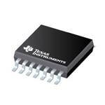
| 描述 | IC INVERTER HEX 14TSSOP |
| 产品分类 | |
| 品牌 | Texas Instruments |
| 数据手册 | |
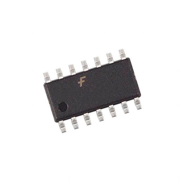
| 产品图片 |
|
| 产品型号 | CD74HCU04QPWRQ1 |
| rohs | 无铅 / 符合限制有害物质指令(RoHS)规范要求 |
| 产品系列 | Automotive, AEC-Q100, 74HCU |
| 不同V、最大CL时的最大传播延迟 | 12ns @ 6V,50pF |
| 供应商器件封装 | 14-TSSOP |
| 其它名称 | 296-27672-1 |
| 包装 | 剪切带 (CT) |
| 安装类型 | 表面贴装 |
| 封装/外壳 | 14-TSSOP(0.173",4.40mm 宽) |
| 工作温度 | -40°C ~ 125°C |
| 标准包装 | 1 |
| 特性 | - |
| 电压-电源 | 2 V ~ 6 V |
| 电流-输出高,低 | 5.2mA,5.2mA |
| 电流-静态(最大值) | 2µA |
| 电路数 | 6 |
| 输入数 | 6 |
| 逻辑电平-低 | 0.3 V ~ 1.1 V |
| 逻辑电平-高 | 1.7 V ~ 4.8 V |
| 逻辑类型 |


- 商务部:美国ITC正式对集成电路等产品启动337调查
- 曝三星4nm工艺存在良率问题 高通将骁龙8 Gen1或转产台积电
- 太阳诱电将投资9.5亿元在常州建新厂生产MLCC 预计2023年完工
- 英特尔发布欧洲新工厂建设计划 深化IDM 2.0 战略
- 台积电先进制程称霸业界 有大客户加持明年业绩稳了
- 达到5530亿美元!SIA预计今年全球半导体销售额将创下新高
- 英特尔拟将自动驾驶子公司Mobileye上市 估值或超500亿美元
- 三星加码芯片和SET,合并消费电子和移动部门,撤换高东真等 CEO
- 三星电子宣布重大人事变动 还合并消费电子和移动部门
- 海关总署:前11个月进口集成电路产品价值2.52万亿元 增长14.8%


PDF Datasheet 数据手册内容提取
Product Order Technical Tools & Support & Folder Now Documents Software Community CD74HCU04-Q1 SCHS381A–JUNE2010–REVISEDAPRIL2020 CD74HCU04-Q1 Automotive Qualified Hex Unbuffered Inverter 1 Features 2 Applications • AEC-Q100Qualifiedforautomotiveapplications: • RCoscillatorcircuit 1 – Devicetemperaturegrade1: • Crystaloscillatorcircuit –40°Cto+125°C,T A 3 Description • Qualifiedforautomotiveapplications The CD74HCU04-Q1 device contains six • Unbufferedlogic independent high-speed CMOS unbuffered inverters. • Positiveandnegativeinputclampdiodes Each inverter performs the Boolean function Y = A in • Wideoperatingvoltagerange:2Vto6V positivelogic. • SignificantpowerreductioncomparedtoLSTTL DeviceInformation(1) logicICs PARTNUMBER PACKAGE BODYSIZE(NOM) CD74HCU04QPWRQ1 TSSOP(14) 5.00mm×4.40mm (1) For all available packages, see the orderable addendum at theendofthedatasheet. FunctionalpinoutoftheCD74HCU04-Q1 VCC (3, 5, 9, 11, 13) 1 2 (4, 6, 8, 10, 12) 1 An IMPORTANT NOTICE at the end of this data sheet addresses availability, warranty, changes, use in safety-critical applications, intellectualpropertymattersandotherimportantdisclaimers.PRODUCTIONDATA.
CD74HCU04-Q1 SCHS381A–JUNE2010–REVISEDAPRIL2020 www.ti.com Table of Contents 1 Features.................................................................. 1 8.3 FeatureDescription...................................................8 2 Applications........................................................... 1 8.4 DeviceFunctionalModes..........................................9 3 Description............................................................. 1 9 ApplicationandImplementation........................ 10 4 RevisionHistory..................................................... 2 9.1 ApplicationInformation............................................10 9.2 TypicalApplication..................................................10 5 PinConfigurationandFunctions......................... 3 10 PowerSupplyRecommendations..................... 13 6 Specifications......................................................... 3 11 Layout................................................................... 13 6.1 AbsoluteMaximumRatings......................................3 6.2 ESDRatings..............................................................4 11.1 LayoutGuidelines.................................................13 6.3 RecommendedOperatingConditions.......................4 11.2 LayoutExample....................................................13 6.4 ThermalInformation..................................................4 12 DeviceandDocumentationSupport................. 14 6.5 ElectricalCharacteristics...........................................5 12.1 DocumentationSupport........................................14 6.6 SwitchingCharacteristics..........................................5 12.2 RelatedLinks........................................................14 6.7 OperatingCharacteristics..........................................5 12.3 CommunityResources..........................................14 6.8 TypicalCharacteristics..............................................6 12.4 Trademarks...........................................................14 7 ParameterMeasurementInformation..................7 12.5 ElectrostaticDischargeCaution............................14 12.6 Glossary................................................................14 8 DetailedDescription.............................................. 8 13 Mechanical,Packaging,andOrderable 8.1 Overview...................................................................8 Information........................................................... 14 8.2 FunctionalBlockDiagram.........................................8 4 Revision History NOTE:Pagenumbersforpreviousrevisionsmaydifferfrompagenumbersinthecurrentversion. ChangesfromRevision(June2010)toRevisionA Page • Updatedtonewdatasheetstandards.................................................................................................................................... 1 • ThermalimpedanceR updatedfrom112.6to121.1°C/W................................................................................................ 4 θJA 2 SubmitDocumentationFeedback Copyright©2010–2020,TexasInstrumentsIncorporated ProductFolderLinks:CD74HCU04-Q1
CD74HCU04-Q1 www.ti.com SCHS381A–JUNE2010–REVISEDAPRIL2020 5 Pin Configuration and Functions PWPackage 14-PinTSSOP TopView 1A 1 14 VCC 1Y 2 13 6A 2A 3 12 6Y 2Y 4 11 5A 3A 5 10 5Y 3Y 6 9 4A GND 7 8 4Y PinFunctions PIN I/O DESCRIPTION NAME NO. 1A 1 Input Channel1,InputA 1Y 2 Output Channel1,OutputY 2A 3 Input Channel2,InputA 2Y 4 Output Channel2,OutputY 3A 5 Input Channel3,InputA 3Y 6 Output Channel3,OutputY GND 7 — Ground 4Y 8 Output Channel4,OutputY 4A 9 Input Channel4,InputA 5Y 10 Output Channel5,OutputY 5A 11 Input Channel5,InputA 6Y 12 Output Channel6,OutputY 6A 13 Input Channel6,InputA V 14 — PositiveSupply CC 6 Specifications 6.1 Absolute Maximum Ratings overoperatingfree-airtemperaturerange(unlessotherwisenoted)(1) MIN MAX UNIT V Supplyvoltage –0.5 7 V CC I Inputclampcurrent(2) V <0orV >V ±20 mA IK I I CC I Outputclampcurrent(2) V <0orV >V ±20 mA OK O O CC I Continuousoutputcurrent V =0toV ±25 mA O O CC ContinuouscurrentthroughV orGND ±50 mA CC T Junctiontemperature(3) 150 °C J T Storagetemperature –65 150 °C stg (1) StressesbeyondthoselistedunderAbsoluteMaximumRatingmaycausepermanentdamagetothedevice.Thesearestressratings only,whichdonotimplyfunctionaloperationofthedeviceattheseoranyotherconditionsbeyondthoseindicatedunderRecommended OperatingCondition.Exposuretoabsolute-maximum-ratedconditionsforextendedperiodsmayaffectdevicereliability. (2) Theinputandoutputvoltageratingsmaybeexceedediftheinputandoutputcurrentratingsareobserved. (3) Guaranteedbydesign. Copyright©2010–2020,TexasInstrumentsIncorporated SubmitDocumentationFeedback 3 ProductFolderLinks:CD74HCU04-Q1
CD74HCU04-Q1 SCHS381A–JUNE2010–REVISEDAPRIL2020 www.ti.com 6.2 ESD Ratings VALUE UNIT Humanbodymodel(HBM),perAECQ100-002(1) ±2000 HBMESDClassificationLevel2 V Electrostaticdischarge V (ESD) Chargeddevicemodel(CDM),perAECQ100- ±1000 011CDMESDClassificationLevelC6 (1) AECQ100-002indicatethatHBMstressingshallbeinaccordancewiththeANSI/ESDA/JEDECJS-001specification. 6.3 Recommended Operating Conditions overoperatingfree-airtemperaturerange(unlessotherwisenoted) MIN NOM MAX UNIT V Supplyvoltage 2 6 V CC V Inputvoltage 0 V V I CC V Outputvoltage 0 V V O CC T Operatingfree-airtemperature –40 125 °C A 6.4 Thermal Information CD74HCU04-Q1 THERMALMETRIC PW(TSSOP) UNIT 14PINS R Junction-to-ambientthermalresistance 121.1 °C/W θJA R Junction-to-case(top)thermalresistance 50.2 °C/W θJC(top) R Junction-to-boardthermalresistance 64.2 °C/W θJB Ψ Junction-to-topcharacterizationparameter 6.1 °C/W JT Ψ Junction-to-boardcharacterizationparameter 63.6 °C/W JB R Junction-to-case(bottom)thermalresistance N/A °C/W θJC(bot) 4 SubmitDocumentationFeedback Copyright©2010–2020,TexasInstrumentsIncorporated ProductFolderLinks:CD74HCU04-Q1
CD74HCU04-Q1 www.ti.com SCHS381A–JUNE2010–REVISEDAPRIL2020 6.5 Electrical Characteristics overoperatingfree-airtemperaturerange;typicalvaluesmeasuredatT =25°C(unlessotherwisenoted). A Operatingfree-airtemperature(T ) A PARAMETER TESTCONDITIONS V 25°C -40°Cto125°C UNIT CC MIN TYP MAX MIN TYP MAX 2V 1.7 1.7 Highlevelinput V 4.5V 3.6 3.6 V IH voltage 6V 4.8 4.8 2V 0.3 0.3 Lowlevelinput V 4.5V 0.8 0.8 V IL voltage 6V 1.1 1.1 2V 1.8 1.8 I =-20µA 4.5V 4.4 4.4 OH High-leveloutput V V =V orV 6V 5.5 5.5 V OH voltage I IH IL I =-4mA 4.5V 3.98 3.7 OH I =-5.2mA 6V 5.48 5.2 OH 2V 0.2 0.2 I =20µA 4.5V 0.5 0.5 OL Low-leveloutput V V =V orV 6V 0.5 0.5 V OL voltage I IH IL I =4mA 4.5V 0.26 0.4 OL I =5.2mA 6V 0.26 0.4 OL Inputleakage I V =V or0 6V ±0.1 ±1 µA I current I CC I Supplycurrent V =V or0 I =0 6V 2 40 µA CC I CC O Input C 2Vto6V 7 pF i capacitance 6.6 Switching Characteristics overoperatingfree-airtemperaturerange(unlessotherwisenoted),C =50pF L Operatingfree-airtemperature(T ) A PARAMETER FROM TO V 25°C –40°Cto125°C UNIT CC MIN TYP MAX MIN TYP MAX 2V 70 105 t Propagationdelay A Y 4.5V 14 21 ns pd 6V 12 18 2V 75 110 t Transition-time Y 4.5V 15 22 ns t 6V 13 19 6.7 Operating Characteristics overoperatingfree-airtemperaturerange;typicalvaluesmeasuredatT =25°C(unlessotherwisenoted). A PARAMETER TESTCONDITIONS MIN TYP MAX UNIT C Powerdissipationcapacitancepergate V =5V,Noload 14 pF pd CC Copyright©2010–2020,TexasInstrumentsIncorporated SubmitDocumentationFeedback 5 ProductFolderLinks:CD74HCU04-Q1
CD74HCU04-Q1 SCHS381A–JUNE2010–REVISEDAPRIL2020 www.ti.com 6.8 Typical Characteristics T =25°C A AMBIENT TEMPERATURE A) 25.0 TA=25oC m 22.5 ( T N 20.0 VCC= 6V E RR 17.5 U C 15.0 ND 12.5 VCC= 4.5V G O 10.0 T CC 7.5 V C, 5.0 C I 2.5 VCC= 2V 0 1 2 3 4 5 6 VI, INPUT VOLTAGE (V) Figure1.TypicalInverterSupplyCurrentasaFunctionofInputVoltage 70 65 AMBIENT TEMPERATURE, TA= 25oC F) 60 VDD= 2V, VI0-2V (p 55 INPUT PIN 5 CONDITIONS CE 50 VDD= 3V, VI0-3V AN 45 VDD= 4V, VI0-4V CIT 40 VDD= 5V, VI0-5V A 35 AP 30 VDD= 6V, VI0-6V C T 25 U P 20 N I 15 C,I 10 5 0 1 2 3 4 5 6 VI,IINPUT VOLTAGE (V) Figure2.InputCapacitanceasaFunctionofInputVoltage 6 SubmitDocumentationFeedback Copyright©2010–2020,TexasInstrumentsIncorporated ProductFolderLinks:CD74HCU04-Q1
CD74HCU04-Q1 www.ti.com SCHS381A–JUNE2010–REVISEDAPRIL2020 7 Parameter Measurement Information • Phase relationships between waveforms were chosen arbitrarily. All input pulses are supplied by generators havingthefollowingcharacteristics:PRR ≤ 1MHz,Z =50 Ω,t < 6ns. O t • Theoutputsaremeasuredoneatatime,withoneinputtransitionpermeasurement. Test 90% 90% VCC Point Input 10% 10% 0 V From Output tr(1) tf(1) Under Test CL(1) 90% 90% VOH Output 10% 10% CL=50pFandincludesprobeandjigcapacitance. tr(1) tf(1) VOL Figure3.LoadCircuit Figure4.VoltageWaveforms TransitionTimes VCC Input 50% 50% 0 V tPLH(1) tPHL(1) VOH Output 50% 50% VOL tPHL(1) tPLH(1) VOH Output 50% 50% VOL Themaximumbetweent andT isusedfort . PLH PHL pd Figure5.VoltageWaveforms PropagationDelays Copyright©2010–2020,TexasInstrumentsIncorporated SubmitDocumentationFeedback 7 ProductFolderLinks:CD74HCU04-Q1
CD74HCU04-Q1 SCHS381A–JUNE2010–REVISEDAPRIL2020 www.ti.com 8 Detailed Description 8.1 Overview TheCD74HCU04-Q1devicecontainssixindependenthigh-speedCMOSunbufferedinverters. 8.2 Functional Block Diagram 1 14 1A VCC 2 13 1Y 6A 3 12 2A 6Y 4 11 2Y 5A 5 10 3A 5Y 6 9 3Y 4A 7 8 GND 4Y 8.3 Feature Description 8.3.1 UnbufferedCMOSLogic Unlike most CMOS logic devices, this device does not include input or output buffers. The input, logic function, andoutputareallcompletedbythesamesetofcomplementaryMOSFETs,asshowninFigure6. VCC (3, 5, 9, 11, 13) 1 2 (4, 6, 8, 10, 12) Figure6. Logicschematicdiagram Each channel of the CD74HCU04-Q1 can drive a load with a total capacitance less than or equal to 50 pF connected to a high-impedance CMOS input while still meeting all of the datasheet specifications. Larger capacitive loads can be applied, however it is not recommended to exceed 70 pF. If larger capacitive loads are required, it is recommended to add a series resistor between the output and the capacitor to limit output current tothevaluesgivenintheAbsoluteMaximumRatings. 8 SubmitDocumentationFeedback Copyright©2010–2020,TexasInstrumentsIncorporated ProductFolderLinks:CD74HCU04-Q1
CD74HCU04-Q1 www.ti.com SCHS381A–JUNE2010–REVISEDAPRIL2020 Feature Description (continued) 8.3.2 ClampDiodeStructure TheinputsandoutputstothisdevicehavebothpositiveandnegativeclampingdiodesasdepictedinFigure7. CAUTION Voltages beyond the values specified in the Absolute Maximum Ratings table can cause damage to the device. The recommended input and output voltage ratings may beexceedediftheinputandoutputclamp-currentratingsareobserved. Device VCC +IIK +IOK Input Logic Output -IIK -IOK GND Figure7. ElectricalPlacementofClampingDiodesforEachInputandOutput 8.4 Device Functional Modes Table1.FunctionTable INPUT OUTPUT A Y L H H L Copyright©2010–2020,TexasInstrumentsIncorporated SubmitDocumentationFeedback 9 ProductFolderLinks:CD74HCU04-Q1
CD74HCU04-Q1 SCHS381A–JUNE2010–REVISEDAPRIL2020 www.ti.com 9 Application and Implementation NOTE Information in the following applications sections is not part of the TI component specification, and TI does not warrant its accuracy or completeness. TI’s customers are responsible for determining suitability of components for their purposes. Customers should validateandtesttheirdesignimplementationtoconfirmsystemfunctionality. 9.1 Application Information In this application, three channels of the CD74HCU04-Q1 are used to create an oscillator circuit as shown in Figure 8. The additional three channels can be used for a second oscillator circuit, used individually for other applications,ortheinputscanbegroundedandthechannelsleftunused. The CD74HCU04-Q1 is used in place of an operational amplifier in an oscillator application. Similar to a conventional inverting amplifier design, this oscillator application depends on factors such as open-loop gain, powerconsumption,andduty-cyclevariation with temperature. Unbuffered inverters have a single inverting stage with an AC signal gain in the range of 10 to 20 dB. Buffered inverters, by definition, have more than one stage of inversion and thus much higher gains, typically in the range of 60 to 70 dB. Due to the lower gain, unbuffered inverters help create a more stable oscillator which is less sensitive to parameter changes. The stability of this typeofoscillatorissufficientforthemajorityofapplicationswithfrequenciesintherangeof100Hzto100kHz. Frequency accuracy is affected by shifts in temperature, manufacturing process, supply voltage, and values of the external timing components. For applications that require an extremely accurate clock, it is recommended to useacrystaloscillatorcircuitoradedicatedoscillatorICinstead. 9.2 Typical Application V CC R C R 2 1 1 V V 0.1 (cid:29)F IN OUT C 2 Figure8. Typicalapplicationschematic 9.2.1 DesignRequirements • Thisdesignutilizesa5-Vsupplyvoltage,resultingina5-Voutputwaveform. • Low variance components should be used for the timing components (R , R , C , C ) as changes in these 1 2 1 2 componentvalueswillcausechangesinoutputfrequency. • ForthisapplicationR musthaveamuchlowervaluethanR (R <<R ). 1 2 1 2 • Shorttracelengthswillimproveoscillatorstabilitybyreducingparasitics. 9.2.1.1 PowerConsiderations Ensure the desired supply voltage is within the range specified in the Recommended Operating Conditions. The supply voltage sets the device's electrical characteristics as described in the Electrical Characteristics. Changes to the supply will change the characteristics of the inverter, which will also change the oscillation frequency slightly. Because the oscillator circuit biases two of the three stages of the device at approximately V /2, both CC MOSFETs in the channels will be turned on and the supply current (I ) through the device will be much larger CC than that shown for operation as a CMOS logic device in the I specification in the Electrical Characteristics. CC Thisvaluewilltypicallybebetween10and30mAperoscillatorcircuit. The supply must be capable of sourcing current equal to the total current to be sourced by all outputs of the CD74HCU04-Q1 plus the maximum supply current, I , listed in the Electrical Characteristics. The logic device CC canonlysourceorsinkasmuchcurrentas it is provided at the supply and ground pins, respectively. Be sure not toexceedthemaximumtotalcurrentthroughGNDorV listedintheAbsoluteMaximumRatings. CC 10 SubmitDocumentationFeedback Copyright©2010–2020,TexasInstrumentsIncorporated ProductFolderLinks:CD74HCU04-Q1
CD74HCU04-Q1 www.ti.com SCHS381A–JUNE2010–REVISEDAPRIL2020 Typical Application (continued) Total power consumption can be calculated using the information provided in CMOS Power Consumption and C Calculation. pd Thermal increase can be calculated using the information provided in Thermal Characteristics of Standard Linear andLogic(SLL)PackagesandDevices. CAUTION The maximum junction temperature, T (max) listed in the Absolute Maximum Ratings, J is an additional limitation to prevent damage to the device. Do not violate any values listed in the Absolute Maximum Ratings. These limits are provided to prevent damage tothedevice. 9.2.1.2 InputConsiderations Although the oscillator circuit described in Application Information does not exactly have an input, the CD74HCU04-Q1 device does have inputs. Be sure to connect all inputs either to a valid logic circuit or as part of the oscillator circuit provided. Attaching oscilloscope probes to nodes of an oscillator circuit can cause shifts in theoperatingfrequency,especiallyifthetimingcapacitorvaluesareverysmall(lessthan100pF). Unused inputs must be terminated to either V or ground. These inputs can be directly terminated if the input is CC completely unused, or they can be connected with a pull-up or pull-down resistor if the input is to be used sometimes,butnotalways.A pull-up resistor is used for a default state of HIGH, and a pull-down resistor is used for a default state of LOW. The resistor size is limited by drive current of the controller, leakage current into the CD74HCU04-Q1, as specified in the Electrical Characteristics, and the desired input transition rate. A 10-kΩ resistorvalueisoftenusedduetothesefactors. RefertotheFeatureDescriptionforadditionalinformationregardingtheinputsforthisdevice. 9.2.1.3 OutputConsiderations The output of the oscillator is a square wave at the supply voltage. This signal can be passed through an additional buffer or inverter stage to add additional drive strength without affecting the operation of the oscillator circuit. The positive supply voltage is used to produce the output HIGH voltage. Drawing current from the output will decrease the output voltage as specified by the V specification in the Electrical Characteristics. Similarly, the OH ground voltage is used to produce the output LOW voltage. Sinking current into the output will increase the output voltage as specified by the V specification in the Electrical Characteristics. Unused outputs can be left OL floating. RefertoFeatureDescriptionforadditionalinformationregardingtheoutputsforthisdevice. 9.2.2 DetailedDesignProcedure 1. Decide the frequency of operation required. Adjustments to the calculated values of the components may be requiredtogetthedesiredfrequency. 2. For the purpose of this design, we will not include C and instead use the internal input capacitance of the 2 buffer which is approximately 15 pF. C should be added to the circuit to reduce overshoot and undershoot 2 conditions on the inputs as shown in Application Curves. Increasing the value of C will slightly decrease the 2 availableoutputfrequency. 3. The simplify the design, R can be set to a large value. 100 kΩ is a good choice. Decreasing R will slightly 2 2 increase the available output frequency but will also increase the overshoot and undershoot on the input of the first buffer as shown in Application Curves. The input signal should never exceed the absolute maximum ratingsofthedevice. 4. Use the equation f = 1/(2.2R C ) to calculate the resistor and capacitor values for the desired frequency. 1 1 KeepinmindtherequirementthatthevalueofR <<R fortheequationtoremainvalid. 1 2 5. Add a decoupling capacitor from V to GND. The capacitor needs to be placed physically close to the CC deviceandelectricallyclosetoboththeV andGNDpins.AnexamplelayoutisshowninLayout. CC Copyright©2010–2020,TexasInstrumentsIncorporated SubmitDocumentationFeedback 11 ProductFolderLinks:CD74HCU04-Q1
CD74HCU04-Q1 SCHS381A–JUNE2010–REVISEDAPRIL2020 www.ti.com Typical Application (continued) 6. Ensure the capacitive load at the output is ≤ 50 pF. This is not a hard limit, however it will ensure optimal performance.Thiscanbeaccomplishedbyproviding short, appropriately sized traces from the CD74HCU04- Q1tothereceivingdevice. 7. Testing this circuit in a simulation tool can be helpful for building confidence in the design, but it is necessary tobuildaprototypetoguaranteeproperoperationasmanyfactorscanimpactthestabilityofthisoscillator. 8. Thermal issues are rarely a concern for logic gates, however the power consumption and thermal increase can be calculated using the steps provided in the application report, CMOS Power Consumption and Cpd Calculation 9.2.3 ApplicationCurves Figure9.Firststageinputwaveformwith Figure10.Firststageinputwaveformwith excessiveovershootandundershoot marginalovershootandundershoot Figure11.Firststageinputwaveformforoptimizedcircuit 12 SubmitDocumentationFeedback Copyright©2010–2020,TexasInstrumentsIncorporated ProductFolderLinks:CD74HCU04-Q1
CD74HCU04-Q1 www.ti.com SCHS381A–JUNE2010–REVISEDAPRIL2020 10 Power Supply Recommendations The power supply can be any voltage between the minimum and maximum supply voltage rating located in the Recommended Operating Conditions. Each V terminal should have a bypass capacitor to prevent power CC disturbance. A 0.1-μF capacitor is recommended for this device. It is acceptable to parallel multiple bypass caps to reject different frequencies of noise. The 0.1-μF and 1-μF capacitors are commonly used in parallel. The bypass capacitor should be installed as close to the power terminal as possible for best results, as shown in Figure12. 11 Layout 11.1 Layout Guidelines When using multiple-input and multiple-channel logic devices inputs must not be left floating. In many cases, functions or parts of functions of digital logic devices are unused; for example, when only two inputs of a triple- input AND gate are used. Such unused input pins must not be left unconnected because the undefined voltages at the outside connections result in undefined operational states. All unused inputs of digital logic devices must be connected to a logic high or logic low voltage, as defined by the input voltage specifications, to prevent them from floating. The logic level that must be applied to any particular unused input depends on the function of the device. Generally, the inputs are tied to GND or V , whichever makes more sense for the logic function or is CC moreconvenient. 11.2 Layout Example Recommend GND flood fill for GND VCC improved signal isolation, noise reduction, and thermal dissipation Bypass capacitor placed close to C2 0.1 (cid:29)F the device R2 1A 1 14 VCC Unused input Short traces 1Y 2 13 6A tied to VCC for oscillator 2A 3 12 6Y Unused output left floating 2Y 4 11 5A C1 3A 5 10 5Y 3Y 6 9 4A R1 GND 7 8 4Y Figure12. ExamplelayoutfortheCD74HCU04-Q1 Copyright©2010–2020,TexasInstrumentsIncorporated SubmitDocumentationFeedback 13 ProductFolderLinks:CD74HCU04-Q1
CD74HCU04-Q1 SCHS381A–JUNE2010–REVISEDAPRIL2020 www.ti.com 12 Device and Documentation Support 12.1 Documentation Support 12.1.1 RelatedDocumentation Forrelateddocumentationseethefollowing: • UseoftheCMOSUnbufferedInverterinOscillatorCircuits • HCMOSDesignConsiderations • CMOSPowerConsumptionandCPDCalculation • DesigningwithLogic 12.2 Related Links The table below lists quick access links. Categories include technical documents, support and community resources,toolsandsoftware,andquickaccesstosampleorbuy. 12.3 Community Resources TI E2E™ support forums are an engineer's go-to source for fast, verified answers and design help — straight fromtheexperts.Searchexistinganswersoraskyourownquestiontogetthequickdesignhelpyouneed. Linked content is provided "AS IS" by the respective contributors. They do not constitute TI specifications and do notnecessarilyreflectTI'sviews;seeTI'sTermsofUse. 12.4 Trademarks E2EisatrademarkofTexasInstruments. Allothertrademarksarethepropertyoftheirrespectiveowners. 12.5 Electrostatic Discharge Caution Thesedeviceshavelimitedbuilt-inESDprotection.Theleadsshouldbeshortedtogetherorthedeviceplacedinconductivefoam duringstorageorhandlingtopreventelectrostaticdamagetotheMOSgates. 12.6 Glossary SLYZ022—TIGlossary. Thisglossarylistsandexplainsterms,acronyms,anddefinitions. 13 Mechanical, Packaging, and Orderable Information The following pages include mechanical, packaging, and orderable information. This information is the most current data available for the designated devices. This data is subject to change without notice and revision of thisdocument.Forbrowser-basedversionsofthisdatasheet,refertotheleft-handnavigation. 14 SubmitDocumentationFeedback Copyright©2010–2020,TexasInstrumentsIncorporated ProductFolderLinks:CD74HCU04-Q1
PACKAGE OPTION ADDENDUM www.ti.com 8-Apr-2020 PACKAGING INFORMATION Orderable Device Status Package Type Package Pins Package Eco Plan Lead/Ball Finish MSL Peak Temp Op Temp (°C) Device Marking Samples (1) Drawing Qty (2) (6) (3) (4/5) CD74HCU04QPWRQ1 ACTIVE TSSOP PW 14 2000 Green (RoHS NIPDAU Level-1-260C-UNLIM -40 to 125 HJU04Q & no Sb/Br) (1) The marketing status values are defined as follows: ACTIVE: Product device recommended for new designs. LIFEBUY: TI has announced that the device will be discontinued, and a lifetime-buy period is in effect. NRND: Not recommended for new designs. Device is in production to support existing customers, but TI does not recommend using this part in a new design. PREVIEW: Device has been announced but is not in production. Samples may or may not be available. OBSOLETE: TI has discontinued the production of the device. (2) RoHS: TI defines "RoHS" to mean semiconductor products that are compliant with the current EU RoHS requirements for all 10 RoHS substances, including the requirement that RoHS substance do not exceed 0.1% by weight in homogeneous materials. Where designed to be soldered at high temperatures, "RoHS" products are suitable for use in specified lead-free processes. TI may reference these types of products as "Pb-Free". RoHS Exempt: TI defines "RoHS Exempt" to mean products that contain lead but are compliant with EU RoHS pursuant to a specific EU RoHS exemption. Green: TI defines "Green" to mean the content of Chlorine (Cl) and Bromine (Br) based flame retardants meet JS709B low halogen requirements of <=1000ppm threshold. Antimony trioxide based flame retardants must also meet the <=1000ppm threshold requirement. (3) MSL, Peak Temp. - The Moisture Sensitivity Level rating according to the JEDEC industry standard classifications, and peak solder temperature. (4) There may be additional marking, which relates to the logo, the lot trace code information, or the environmental category on the device. (5) Multiple Device Markings will be inside parentheses. Only one Device Marking contained in parentheses and separated by a "~" will appear on a device. If a line is indented then it is a continuation of the previous line and the two combined represent the entire Device Marking for that device. (6) Lead/Ball Finish - Orderable Devices may have multiple material finish options. Finish options are separated by a vertical ruled line. Lead/Ball Finish values may wrap to two lines if the finish value exceeds the maximum column width. Important Information and Disclaimer:The information provided on this page represents TI's knowledge and belief as of the date that it is provided. TI bases its knowledge and belief on information provided by third parties, and makes no representation or warranty as to the accuracy of such information. Efforts are underway to better integrate information from third parties. TI has taken and continues to take reasonable steps to provide representative and accurate information but may not have conducted destructive testing or chemical analysis on incoming materials and chemicals. TI and TI suppliers consider certain information to be proprietary, and thus CAS numbers and other limited information may not be available for release. In no event shall TI's liability arising out of such information exceed the total purchase price of the TI part(s) at issue in this document sold by TI to Customer on an annual basis. OTHER QUALIFIED VERSIONS OF CD74HCU04-Q1 : Addendum-Page 1
PACKAGE OPTION ADDENDUM www.ti.com 8-Apr-2020 •Catalog: CD74HCU04 NOTE: Qualified Version Definitions: •Catalog - TI's standard catalog product Addendum-Page 2
None
IMPORTANTNOTICEANDDISCLAIMER TI PROVIDES TECHNICAL AND RELIABILITY DATA (INCLUDING DATASHEETS), DESIGN RESOURCES (INCLUDING REFERENCE DESIGNS), APPLICATION OR OTHER DESIGN ADVICE, WEB TOOLS, SAFETY INFORMATION, AND OTHER RESOURCES “AS IS” AND WITH ALL FAULTS, AND DISCLAIMS ALL WARRANTIES, EXPRESS AND IMPLIED, INCLUDING WITHOUT LIMITATION ANY IMPLIED WARRANTIES OF MERCHANTABILITY, FITNESS FOR A PARTICULAR PURPOSE OR NON-INFRINGEMENT OF THIRD PARTY INTELLECTUAL PROPERTY RIGHTS. These resources are intended for skilled developers designing with TI products. You are solely responsible for (1) selecting the appropriate TI products for your application, (2) designing, validating and testing your application, and (3) ensuring your application meets applicable standards, and any other safety, security, or other requirements. These resources are subject to change without notice. TI grants you permission to use these resources only for development of an application that uses the TI products described in the resource. Other reproduction and display of these resources is prohibited. No license is granted to any other TI intellectual property right or to any third party intellectual property right. TI disclaims responsibility for, and you will fully indemnify TI and its representatives against, any claims, damages, costs, losses, and liabilities arising out of your use of these resources. TI’s products are provided subject to TI’s Terms of Sale (www.ti.com/legal/termsofsale.html) or other applicable terms available either on ti.com or provided in conjunction with such TI products. TI’s provision of these resources does not expand or otherwise alter TI’s applicable warranties or warranty disclaimers for TI products. Mailing Address: Texas Instruments, Post Office Box 655303, Dallas, Texas 75265 Copyright © 2020, Texas Instruments Incorporated