ICGOO在线商城 > 集成电路(IC) > 逻辑 - 信号开关,多路复用器,解码器 > CD74HC147E
 Datasheet下载
- 型号: CD74HC147E
- 制造商: Texas Instruments
- 库位|库存: xxxx|xxxx
- 要求:
| 数量阶梯 | 香港交货 | 国内含税 |
| +xxxx | $xxxx | ¥xxxx |
查看当月历史价格
查看今年历史价格
CD74HC147E产品简介:
ICGOO电子元器件商城为您提供CD74HC147E由Texas Instruments设计生产,在icgoo商城现货销售,并且可以通过原厂、代理商等渠道进行代购。 CD74HC147E价格参考¥1.22-¥3.50。Texas InstrumentsCD74HC147E封装/规格:逻辑 - 信号开关,多路复用器,解码器, Priority Encoder 1 x 10:4 16-PDIP。您可以下载CD74HC147E参考资料、Datasheet数据手册功能说明书,资料中有CD74HC147E 详细功能的应用电路图电压和使用方法及教程。
Texas Instruments(德州仪器)的CD74HC147E是一款逻辑信号开关、多路复用器和解码器,属于74HC系列高速CMOS器件。该芯片主要用于将多个输入信号转换为较少的输出信号,适用于多种应用场景。

 主要功能
CD74HC147E是一个优先编码器(Priority Encoder),能够将8个输入信号中的最高优先级有效输入转换为对应的4位二进制代码输出。它的工作电压范围宽(2V至6V),具有低功耗和高噪声容限的特点,适用于各种数字电路设计。

 应用场景

1. 键盘扫描:
   - 在键盘矩阵中,CD74HC147E可以用于检测按键状态并将其编码为相应的二进制值。由于其优先编码特性,当多个按键同时按下时,它会优先处理较高优先级的按键,确保系统的响应准确性。

2. 多路信号选择:
   - 在需要从多个输入源中选择一个或几个信号进行处理的应用中,如音频切换、视频信号选择等,CD74HC147E可以简化电路设计,减少外部元件数量。

3. 中断请求管理:
   - 在嵌入式系统中,多个外设可能同时产生中断请求。CD74HC147E可以用于管理和优先处理这些中断请求,确保高优先级的中断首先被响应,从而提高系统的实时性和可靠性。

4. 数据采集系统:
   - 在多通道数据采集系统中,CD74HC147E可以帮助识别哪个通道有有效的输入信号,并将其编码为地址信息,供后续的数据处理模块使用。

5. 工业控制:
   - 在工业自动化控制系统中,CD74HC147E可用于监测多个传感器的状态,并将这些状态信息编码后传输给中央控制器,实现高效的状态监控和故障诊断。

6. 通信接口:
   - 在某些通信协议中,CD74HC147E可以用于解析接收到的多路信号,确定哪个通道有有效的数据传输,并进行相应的处理。

总之,CD74HC147E凭借其高效的优先编码功能,在需要处理多个输入信号并进行快速响应的场景中表现出色,广泛应用于各类电子设备和系统中。
| 参数 | 数值 |
| 产品目录 | 集成电路 (IC)半导体 |
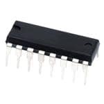
| 描述 | IC 10-4LN PRIORTY ENCODER 16DIP编码器、解码器、复用器和解复用器 Line Priority Encodr |
| 产品分类 | |
| 品牌 | Texas Instruments |
| 产品手册 | |
| 产品图片 |
|
| rohs | 符合RoHS无铅 / 符合限制有害物质指令(RoHS)规范要求 |
| 产品系列 | 逻辑集成电路,编码器、解码器、复用器和解复用器,Texas Instruments CD74HC147E74HC |
| 数据手册 | |
| 产品型号 | CD74HC147E |
| PCN设计/规格 | |
| 产品 | Priority Encoders |
| 产品目录页面 | |
| 产品种类 | 编码器、解码器、复用器和解复用器 |
| 传播延迟时间 | 13 ns |
| 供应商器件封装 | 16-PDIP |
| 其它名称 | 296-14513-5 |
| 包装 | 管件 |
| 单位重量 | 1 g |
| 商标 | Texas Instruments |
| 安装类型 | 通孔 |
| 安装风格 | Through Hole |
| 封装 | Tube |
| 封装/外壳 | 16-DIP(0.300",7.62mm) |
| 封装/箱体 | PDIP-16 |
| 工作温度 | -55°C ~ 125°C |
| 工作温度范围 | - 55 C to + 125 C |
| 工作电压 | 2 V to 6 V |
| 工厂包装数量 | 25 |
| 最大工作温度 | + 125 C |
| 最小工作温度 | - 55 C |
| 标准包装 | 25 |
| 独立电路 | 1 |
| 电压-电源 | 2 V ~ 6 V |
| 电压源 | 单电源 |
| 电流-输出高,低 | 5.2mA,5.2mA |
| 电源电压-最大 | 6 V |
| 电源电压-最小 | 2 V |
| 电路 | 1 x 10:4 |
| 类型 | 优先顺序编码器 |
| 系列 | CD74HC147 |
| 输入/输出线数量 | 10 / 4 |
| 输入线路数量 | 10 |
| 输出线路数量 | 4 |
| 逻辑系列 | HC |


- 商务部:美国ITC正式对集成电路等产品启动337调查
- 曝三星4nm工艺存在良率问题 高通将骁龙8 Gen1或转产台积电
- 太阳诱电将投资9.5亿元在常州建新厂生产MLCC 预计2023年完工
- 英特尔发布欧洲新工厂建设计划 深化IDM 2.0 战略
- 台积电先进制程称霸业界 有大客户加持明年业绩稳了
- 达到5530亿美元!SIA预计今年全球半导体销售额将创下新高
- 英特尔拟将自动驾驶子公司Mobileye上市 估值或超500亿美元
- 三星加码芯片和SET,合并消费电子和移动部门,撤换高东真等 CEO
- 三星电子宣布重大人事变动 还合并消费电子和移动部门
- 海关总署:前11个月进口集成电路产品价值2.52万亿元 增长14.8%


PDF Datasheet 数据手册内容提取
CD54HC147, CD74HC147, CD74HCT147 Data sheet acquired from Harris Semiconductor SCHS149F High-Speed CMOS Logic 10- to 4-Line Priority Encoder September 1997 - Revised November 2003 Features providebinaryrepresentationonthefouractiveLOWinputs [ /Title (Y0toY3).Apriorityisassignedtoeachinputsothatwhen (CD74 • Buffered Inputs and Outputs two or more inputs are simultaneously active, the input with the highest priority is represented on the output, with input HC147 • Typical Propagation Delay: 13ns at VCC = 5V, , CL = 15pF, TA = 25oC line l9 having the highest priority. Thesedevicesprovidethe10-lineto4-linepriorityencoding CD74 • Fanout (Over Temperature Range) function by use of the implied decimal “zero”. The “zero” is HCT14 - Standard Outputs. . . . . . . . . . . . . . .10 LSTTL Loads encodedwhenallninedatainputsareHIGH,forcingallfour 7) - Bus Driver Outputs . . . . . . . . . . . . .15 LSTTL Loads outputs HIGH. /Sub- • Wide Operating Temperature Range . . .-55oC to 125oC Ordering Information ject • Balanced Propagation Delay and Transition Times (High • Significant Power Reduction Compared to LSTTL TEMP. RANGE Speed PART NUMBER (oC) PACKAGE Logic ICs CMOS • HC Types CD54HC147F3A -55 to 125 16 Ld CERDIP Logic - 2V to 6V Operation CD74HC147E -55 to 125 16 Ld PDIP 10-to-4 - High Noise Immunity: NIL = 30%, NIH = 30% of VCC Line at VCC = 5V CD74HC147M -55 to 125 16 Ld SOIC Prior- • HCT Types CD74HC147MT -55 to 125 16 Ld SOIC ity - 4.5V to 5.5V Operation CD74HC147M96 -55 to 125 16 Ld SOIC Encode - Direct LSTTL Input Logic Compatibility, CD74HC147NSR -55 to 125 16 Ld SOP r) VIL= 0.8V (Max), VIH = 2V (Min) /Autho - CMOS Input Compatibility, Il≤1µA at VOL, VOH CD74HC147PW -55 to 125 16 Ld TSSOP r () CD74HC147PWR -55 to 125 16 Ld TSSOP Description /Key- CD74HC147PWT -55 to 125 16 Ld TSSOP words The ’HC147 and CD74HCT147 are high speed silicon-gate (High CMOS devices and are pin-compatible with low power CD74HCT147E -55 to 125 16 Ld PDIP Schottky TTL (LSTTL). Speed NOTE: Whenordering,usetheentirepartnumber.Thesuffixes CMOS The ’HC147 and CD74HCT147 9-input priority encoders 96 and R denote tape and reel. The suffix T denotes a accept data from nine active LOW inputs (l1 to l9) and small-quantity reel of 250. Logic 10-to-4 Line Pinout Prior- CD54HC147 (CERDIP) ity CD74HC147 (PDIP, SOIC, SOP, TSSOP) CD74HCT147 (PDIP, TSSOP) Encode TOP VIEW r,High Speed I4 1 16 VCC CMOS I5 2 15 NC Logic I6 3 14 Y3 10-to-4 I7 4 13 I3 Line I8 5 12 I2 Prior- Y2 6 11 I1 ity Y1 7 10 I9 GND 8 9 Y0 CAUTION: These devices are sensitive to electrostatic discharge. Users should follow proper IC Handling Procedures. Copyright © 2003, Texas Instruments Incorporated 1
CD54HC147, CD74HC147, CD74HCT147 Functional Diagram 11 I1 9 12 I2 Y0 13 I3 1 7 I4 Y1 2 I5 3 6 I6 Y2 4 I7 5 14 I8 Y3 10 I9 GND = 8 VCC = 16 TRUTH TABLE INPUTS OUTPUTS I1 I2 I3 I4 I5 I6 I7 I8 I9 Y3 Y2 Y1 Y0 H H H H H H H H H H H H H X X X X X X X X L L H H L X X X X X X X L H L H H H X X X X X X L H H H L L L X X X X X L H H H H L L H X X X X L H H H H H L H L X X X L H H H H H H L H H X X L H H H H H H H H L L X L H H H H H H H H H L H L H H H H H H H H H H H L H = High Logic Level, L = Low Logic Level, X = Don’t Care 2
CD54HC147, CD74HC147, CD74HCT147 Absolute Maximum Ratings Thermal Information DC Supply Voltage, VCC . . . . . . . . . . . . . . . . . . . . . . . . -0.5V to 7V Package Thermal Impedance,θJA(see Note 1): DC Input Diode Current, IIK E (PDIP) Package . . . . . . . . . . . . . . . . . . . . . . . . . . . . . . .67oC/W For VI < -0.5V or VI > VCC + 0.5V. . . . . . . . . . . . . . . . . . . . . .±20mA M (SOIC) Package. . . . . . . . . . . . . . . . . . . . . . . . . . . . . . .73oC/W DC Output Diode Current, IOK NS (SOP) Package . . . . . . . . . . . . . . . . . . . . . . . . . . . . . 64oC/W For VO < -0.5V or VO > VCC + 0.5V . . . . . . . . . . . . . . . . . . . .±20mA PW (TSSOP) Package . . . . . . . . . . . . . . . . . . . . . . . . . 108oC/W DC Output Source or Sink Current per Output Pin, IO Maximum Junction Temperature. . . . . . . . . . . . . . . . . . . . . . .150oC For VO > -0.5V or VO < VCC + 0.5V . . . . . . . . . . . . . . . . . . . .±25mA Maximum Storage Temperature Range . . . . . . . . . .-65oC to 150oC DC VCC or Ground Current, ICC orIGND. . . . . . . . . . . . . . . . . .±50mA Maximum Lead Temperature (Soldering 10s). . . . . . . . . . . . .300oC (SOIC - Lead Tips Only) Operating Conditions Temperature Range (TA) . . . . . . . . . . . . . . . . . . . . .-55oC to 125oC Supply Voltage Range, VCC HC Types . . . . . . . . . . . . . . . . . . . . . . . . . . . . . . . . . . . . .2V to 6V HCT Types . . . . . . . . . . . . . . . . . . . . . . . . . . . . . . . . .4.5V to 5.5V DC Input or Output Voltage, VI, VO . . . . . . . . . . . . . . . . . 0V to VCC Input Rise and Fall Time 2V . . . . . . . . . . . . . . . . . . . . . . . . . . . . . . . . . . . . . . 1000ns (Max) 4.5V. . . . . . . . . . . . . . . . . . . . . . . . . . . . . . . . . . . . . . 500ns (Max) 6V . . . . . . . . . . . . . . . . . . . . . . . . . . . . . . . . . . . . . . . 400ns (Max) CAUTION:Stressesabovethoselistedin“AbsoluteMaximumRatings”maycausepermanentdamagetothedevice.Thisisastressonlyratingandoperation of the device at these or any other conditions above those indicated in the operational sections of this specification is not implied. NOTE: 1. The package thermal impedance is calculated in accordance with JESD 51-7. DC Electrical Specifications TEST CONDITIONS 25oC -40oC TO 85oC -55oCTO125oC VCC PARAMETER SYMBOL VI(V) IO(mA) (V) MIN TYP MAX MIN MAX MIN MAX UNITS HC TYPES High Level Input VIH - - 2 1.5 - - 1.5 - 1.5 - V Voltage 4.5 3.15 - - 3.15 - 3.15 - V 6 4.2 - - 4.2 - 4.2 - V Low Level Input VIL - - 2 - - 0.5 - 0.5 - 0.5 V Voltage 4.5 - - 1.35 - 1.35 - 1.35 V 6 - - 1.8 - 1.8 - 1.8 V High Level Output VOH VIHorVIL -0.02 2 1.9 - - 1.9 - 1.9 - V Voltage -0.02 4.5 4.4 - - 4.4 - 4.4 - V CMOS Loads -0.02 6 5.9 - - 5.9 - 5.9 - V High Level Output - - - - - - - - - V Voltage -4 4.5 3.98 - - 3.84 - 3.7 - V TTL Loads -5.2 6 5.48 - - 5.34 - 5.2 - V Low Level Output VOL VIHorVIL 0.02 2 - - 0.1 - 0.1 - 0.1 V Voltage 0.02 4.5 - - 0.1 - 0.1 - 0.1 V CMOS Loads 0.02 6 - - 0.1 - 0.1 - 0.1 V Low Level Output - - - - - - - - - V Voltage 4 4.5 - - 0.26 - 0.33 - 0.4 V TTL Loads 5.2 6 - - 0.26 - 0.33 - 0.4 V Input Leakage II VCC or - 6 - - ±0.1 - ±1 - ±1 µA Current GND Quiescent Device ICC VCC or 0 6 - - 8 - 80 - 160 µA Current GND 3
CD54HC147, CD74HC147, CD74HCT147 DC Electrical Specifications (Continued) TEST CONDITIONS 25oC -40oC TO 85oC -55oCTO125oC VCC PARAMETER SYMBOL VI(V) IO(mA) (V) MIN TYP MAX MIN MAX MIN MAX UNITS HCT TYPES High Level Input VIH - - 4.5 to 2 - - 2 - 2 - V Voltage 5.5 Low Level Input VIL - - 4.5 to - - 0.8 - 0.8 - 0.8 V Voltage 5.5 High Level Output VOH VIHorVIL -0.02 4.5 4.4 - - 4.4 - 4.4 - V Voltage CMOS Loads High Level Output -4 4.5 3.98 - - 3.84 - 3.7 - V Voltage TTL Loads Low Level Output VOL VIHorVIL 0.02 4.5 - - 0.1 - 0.1 - 0.1 V Voltage CMOS Loads Low Level Output 4 4.5 - - 0.26 - 0.33 - 0.4 V Voltage TTL Loads Input Leakage II VCCand 0 5.5 - ±0.1 - ±1 - ±1 µA Current GND Quiescent Device ICC VCC or 0 5.5 - - 8 - 80 - 160 µA Current GND Additional Quiescent ∆ICC VCC - 4.5 to - 100 360 - 450 - 490 µA Device Current Per (Note 2) -2.1 5.5 Input Pin: 1 Unit Load NOTE: 2. For dual-supply systems theoretical worst case (VI = 2.4V, VCC = 5.5V) specification is 1.8mA. HCT Input Loading Table INPUT UNIT LOADS I1,I2,I3,I6,I7 1.1 I4,I5,I8,I9 1.5 NOTE: UnitLoadis∆ICClimitspecifiedinDCElectricalTable,e.g., 360µA max at 25oC. Switching SpecificationsInput tr, tf = 6ns 25oC -40oC TO 85oC -55oC TO 125oC TEST PARAMETER SYMBOL CONDITIONS VCC(V) MIN TYP MAX MIN MAX MIN MAX UNITS HC TYPES Propagation Delay, tPLH,tPHL CL= 50pF 2 - - 160 - 200 - 240 ns Input to Output (Figure 1) 4.5 - - 32 - 40 - 48 ns 5 - 13 - - - - - ns 6 - - 27 - 34 - 41 ns Transition Times tTLH, tTHL CL= 50pF 2 - - 75 - 95 - 110 ns (Figure 1) 4.5 - - 15 - 19 - 22 ns 6 - - 13 - 16 - 19 ns Input Capacitance CIN - - - - 10 - 10 - 10 pF 4
CD54HC147, CD74HC147, CD74HCT147 Switching SpecificationsInput tr, tf = 6ns (Continued) 25oC -40oC TO 85oC -55oC TO 125oC TEST PARAMETER SYMBOL CONDITIONS VCC(V) MIN TYP MAX MIN MAX MIN MAX UNITS Power Dissipation Capaci- CPD - 5 - 32 - - - - - pF tance (Notes 3, 4) HCT TYPES Propagation Delay, tPLH, tPHL CL= 50pF 4.5 - - 35 - 44 - 53 ns Input to Output (Figure 2) 5 - 14 - - - - - ns Transition Times (Figure 2) tTLH, tTHL CL= 50pF 4.5 - - 15 - 19 - 22 ns Input Capacitance CIN - - - - 10 - 10 - 10 pF Power Dissipation Capaci- CPD - 5 - 42 - - - - - pF tance (Notes 3, 4) NOTES: 3. CPD is used to determine the dynamic power consumption, per gate. 4. PD = VCC2 fi(CPD + CL) where fi = Input Frequency, CL = Output Load Capacitance, VCC = Supply Voltage. Test Circuits and Waveforms tr = 6ns tf = 6ns tr = 6ns tf = 6ns 90% VCC 2.7V 3V INPUT 50% INPUT 1.3V 10% GND 0.3V GND tTHL tTLH tTHL tTLH 90% 90% 50% INVERTING 10% INVERTING 1.3V OUTPUT OUTPUT 10% tPHL tPLH tPHL tPLH FIGURE6. HCANDHCUTRANSITIONTIMESANDPROPAGA- FIGURE7. HCTTRANSITIONTIMESANDPROPAGATION TION DELAY TIMES, COMBINATION LOGIC DELAY TIMES, COMBINATION LOGIC 5
PACKAGE OPTION ADDENDUM www.ti.com 6-Feb-2020 PACKAGING INFORMATION Orderable Device Status Package Type Package Pins Package Eco Plan Lead/Ball Finish MSL Peak Temp Op Temp (°C) Device Marking Samples (1) Drawing Qty (2) (6) (3) (4/5) 8406401EA ACTIVE CDIP J 16 1 TBD Call TI N / A for Pkg Type -55 to 125 8406401EA CD54HC147F3A CD54HC147F3A ACTIVE CDIP J 16 1 TBD Call TI N / A for Pkg Type -55 to 125 8406401EA CD54HC147F3A CD74HC147E ACTIVE PDIP N 16 25 Green (RoHS NIPDAU N / A for Pkg Type -55 to 125 CD74HC147E & no Sb/Br) CD74HC147M ACTIVE SOIC D 16 40 Green (RoHS NIPDAU Level-1-260C-UNLIM -55 to 125 HC147M & no Sb/Br) CD74HC147M96 ACTIVE SOIC D 16 2500 Green (RoHS NIPDAU Level-1-260C-UNLIM -55 to 125 HC147M & no Sb/Br) CD74HC147M96E4 ACTIVE SOIC D 16 2500 Green (RoHS NIPDAU Level-1-260C-UNLIM -55 to 125 HC147M & no Sb/Br) CD74HC147MT ACTIVE SOIC D 16 250 Green (RoHS NIPDAU Level-1-260C-UNLIM -55 to 125 HC147M & no Sb/Br) CD74HC147PW ACTIVE TSSOP PW 16 90 Green (RoHS NIPDAU Level-1-260C-UNLIM -55 to 125 HJ147 & no Sb/Br) CD74HC147PWR ACTIVE TSSOP PW 16 2000 Green (RoHS NIPDAU Level-1-260C-UNLIM -55 to 125 HJ147 & no Sb/Br) CD74HC147PWT ACTIVE TSSOP PW 16 250 Green (RoHS NIPDAU Level-1-260C-UNLIM -55 to 125 HJ147 & no Sb/Br) CD74HCT147E ACTIVE PDIP N 16 25 Green (RoHS NIPDAU N / A for Pkg Type -55 to 125 CD74HCT147E & no Sb/Br) (1) The marketing status values are defined as follows: ACTIVE: Product device recommended for new designs. LIFEBUY: TI has announced that the device will be discontinued, and a lifetime-buy period is in effect. NRND: Not recommended for new designs. Device is in production to support existing customers, but TI does not recommend using this part in a new design. PREVIEW: Device has been announced but is not in production. Samples may or may not be available. OBSOLETE: TI has discontinued the production of the device. (2) RoHS: TI defines "RoHS" to mean semiconductor products that are compliant with the current EU RoHS requirements for all 10 RoHS substances, including the requirement that RoHS substance do not exceed 0.1% by weight in homogeneous materials. Where designed to be soldered at high temperatures, "RoHS" products are suitable for use in specified lead-free processes. TI may reference these types of products as "Pb-Free". RoHS Exempt: TI defines "RoHS Exempt" to mean products that contain lead but are compliant with EU RoHS pursuant to a specific EU RoHS exemption. Green: TI defines "Green" to mean the content of Chlorine (Cl) and Bromine (Br) based flame retardants meet JS709B low halogen requirements of <=1000ppm threshold. Antimony trioxide based flame retardants must also meet the <=1000ppm threshold requirement. Addendum-Page 1
PACKAGE OPTION ADDENDUM www.ti.com 6-Feb-2020 (3) MSL, Peak Temp. - The Moisture Sensitivity Level rating according to the JEDEC industry standard classifications, and peak solder temperature. (4) There may be additional marking, which relates to the logo, the lot trace code information, or the environmental category on the device. (5) Multiple Device Markings will be inside parentheses. Only one Device Marking contained in parentheses and separated by a "~" will appear on a device. If a line is indented then it is a continuation of the previous line and the two combined represent the entire Device Marking for that device. (6) Lead/Ball Finish - Orderable Devices may have multiple material finish options. Finish options are separated by a vertical ruled line. Lead/Ball Finish values may wrap to two lines if the finish value exceeds the maximum column width. Important Information and Disclaimer:The information provided on this page represents TI's knowledge and belief as of the date that it is provided. TI bases its knowledge and belief on information provided by third parties, and makes no representation or warranty as to the accuracy of such information. Efforts are underway to better integrate information from third parties. TI has taken and continues to take reasonable steps to provide representative and accurate information but may not have conducted destructive testing or chemical analysis on incoming materials and chemicals. TI and TI suppliers consider certain information to be proprietary, and thus CAS numbers and other limited information may not be available for release. In no event shall TI's liability arising out of such information exceed the total purchase price of the TI part(s) at issue in this document sold by TI to Customer on an annual basis. OTHER QUALIFIED VERSIONS OF CD54HC147, CD74HC147 : •Catalog: CD74HC147 •Military: CD54HC147 NOTE: Qualified Version Definitions: •Catalog - TI's standard catalog product •Military - QML certified for Military and Defense Applications Addendum-Page 2
PACKAGE MATERIALS INFORMATION www.ti.com 14-Jul-2012 TAPE AND REEL INFORMATION *Alldimensionsarenominal Device Package Package Pins SPQ Reel Reel A0 B0 K0 P1 W Pin1 Type Drawing Diameter Width (mm) (mm) (mm) (mm) (mm) Quadrant (mm) W1(mm) CD74HC147M96 SOIC D 16 2500 330.0 16.4 6.5 10.3 2.1 8.0 16.0 Q1 CD74HC147PWR TSSOP PW 16 2000 330.0 12.4 6.9 5.6 1.6 8.0 12.0 Q1 CD74HC147PWT TSSOP PW 16 250 330.0 12.4 6.9 5.6 1.6 8.0 12.0 Q1 PackMaterials-Page1
PACKAGE MATERIALS INFORMATION www.ti.com 14-Jul-2012 *Alldimensionsarenominal Device PackageType PackageDrawing Pins SPQ Length(mm) Width(mm) Height(mm) CD74HC147M96 SOIC D 16 2500 333.2 345.9 28.6 CD74HC147PWR TSSOP PW 16 2000 367.0 367.0 35.0 CD74HC147PWT TSSOP PW 16 250 367.0 367.0 35.0 PackMaterials-Page2
None
None
None
None
PACKAGE OUTLINE PW0016A TSSOP - 1.2 mm max height SCALE 2.500 SMALL OUTLINE PACKAGE SEATING PLANE C 6.6 TYP 6.2 A 0.1 C PIN 1 INDEX AREA 14X 0.65 16 1 2X 5.1 4.55 4.9 NOTE 3 8 9 0.30 B 4.5 16X 0.19 1.2 MAX 4.3 0.1 C A B NOTE 4 (0.15) TYP SEE DETAIL A 0.25 GAGE PLANE 0.15 0.05 0.75 0.50 0 -8 DETA 20AIL A TYPICAL 4220204/A 02/2017 NOTES: 1. All linear dimensions are in millimeters. Any dimensions in parenthesis are for reference only. Dimensioning and tolerancing per ASME Y14.5M. 2. This drawing is subject to change without notice. 3. This dimension does not include mold flash, protrusions, or gate burrs. Mold flash, protrusions, or gate burrs shall not exceed 0.15 mm per side. 4. This dimension does not include interlead flash. Interlead flash shall not exceed 0.25 mm per side. 5. Reference JEDEC registration MO-153. www.ti.com
EXAMPLE BOARD LAYOUT PW0016A TSSOP - 1.2 mm max height SMALL OUTLINE PACKAGE 16X (1.5) SYMM (R0.05) TYP 1 16X (0.45) 16 SYMM 14X (0.65) 8 9 (5.8) LAND PATTERN EXAMPLE EXPOSED METAL SHOWN SCALE: 10X SOLDER MASK METAL UNDER SOLDER MASK OPENING METAL SOLDER MASK OPENING EXPOSED METAL EXPOSED METAL 0.05 MAX 0.05 MIN ALL AROUND ALL AROUND NON-SOLDER MASK SOLDER MASK DEFINED DEFINED (PREFERRED) SOLDE15.000R MASK DETAILS 4220204/A 02/2017 NOTES: (continued) 6. Publication IPC-7351 may have alternate designs. 7. Solder mask tolerances between and around signal pads can vary based on board fabrication site. www.ti.com
EXAMPLE STENCIL DESIGN PW0016A TSSOP - 1.2 mm max height SMALL OUTLINE PACKAGE 16X (1.5) SYMM (R0.05) TYP 1 16X (0.45) 16 SYMM 14X (0.65) 8 9 (5.8) SOLDER PASTE EXAMPLE BASED ON 0.125 mm THICK STENCIL SCALE: 10X 4220204/A 02/2017 NOTES: (continued) 8. Laser cutting apertures with trapezoidal walls and rounded corners may offer better paste release. IPC-7525 may have alternate design recommendations. 9. Board assembly site may have different recommendations for stencil design. www.ti.com
IMPORTANTNOTICEANDDISCLAIMER TI PROVIDES TECHNICAL AND RELIABILITY DATA (INCLUDING DATASHEETS), DESIGN RESOURCES (INCLUDING REFERENCE DESIGNS), APPLICATION OR OTHER DESIGN ADVICE, WEB TOOLS, SAFETY INFORMATION, AND OTHER RESOURCES “AS IS” AND WITH ALL FAULTS, AND DISCLAIMS ALL WARRANTIES, EXPRESS AND IMPLIED, INCLUDING WITHOUT LIMITATION ANY IMPLIED WARRANTIES OF MERCHANTABILITY, FITNESS FOR A PARTICULAR PURPOSE OR NON-INFRINGEMENT OF THIRD PARTY INTELLECTUAL PROPERTY RIGHTS. These resources are intended for skilled developers designing with TI products. You are solely responsible for (1) selecting the appropriate TI products for your application, (2) designing, validating and testing your application, and (3) ensuring your application meets applicable standards, and any other safety, security, or other requirements. These resources are subject to change without notice. TI grants you permission to use these resources only for development of an application that uses the TI products described in the resource. Other reproduction and display of these resources is prohibited. No license is granted to any other TI intellectual property right or to any third party intellectual property right. TI disclaims responsibility for, and you will fully indemnify TI and its representatives against, any claims, damages, costs, losses, and liabilities arising out of your use of these resources. TI’s products are provided subject to TI’s Terms of Sale (www.ti.com/legal/termsofsale.html) or other applicable terms available either on ti.com or provided in conjunction with such TI products. TI’s provision of these resources does not expand or otherwise alter TI’s applicable warranties or warranty disclaimers for TI products. Mailing Address: Texas Instruments, Post Office Box 655303, Dallas, Texas 75265 Copyright © 2020, Texas Instruments Incorporated