ICGOO在线商城 > 集成电路(IC) > 时钟/计时 - 可编程计时器和振荡器 > CD4541BNSR
 Datasheet下载
- 型号: CD4541BNSR
- 制造商: Texas Instruments
- 库位|库存: xxxx|xxxx
- 要求:
| 数量阶梯 | 香港交货 | 国内含税 |
| +xxxx | $xxxx | ¥xxxx |
查看当月历史价格
查看今年历史价格
CD4541BNSR产品简介:
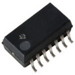
ICGOO电子元器件商城为您提供CD4541BNSR由Texas Instruments设计生产,在icgoo商城现货销售,并且可以通过原厂、代理商等渠道进行代购。 CD4541BNSR价格参考。Texas InstrumentsCD4541BNSR封装/规格:时钟/计时 - 可编程计时器和振荡器, Programmable Timer IC 65536 Count 100kHz 14-SOP。您可以下载CD4541BNSR参考资料、Datasheet数据手册功能说明书,资料中有CD4541BNSR 详细功能的应用电路图电压和使用方法及教程。
Texas Instruments 的 CD4541BNSR 是一款可编程定时器/计时器集成电路,属于时钟和计时器件系列。它广泛应用于需要精确延时或定时控制的电子系统中。

该芯片主要应用于以下场景:

1. 工业控制系统:用于实现设备启动延迟、关闭延时或周期性操作控制,如电机启动延时保护、加热系统定时控制等。

2. 消费电子产品:如家电中的定时功能模块,包括微波炉、洗衣机、电饭煲等,实现按键操作后的延时响应或运行时间控制。

3. 安防系统:在报警系统中用于设置警报触发后的持续时间,或在摄像头系统中用于控制灯光或录像的定时开启与关闭。

4. 汽车电子:用于车灯延时关闭(如“伴我回家”功能)、雨刷间歇控制、风扇定时关闭等功能。

5. 仪器仪表:用于测试设备中的定时采样、数据记录的时间间隔控制等。

CD4541BNSR 采用 16 引脚 SOIC 封装,具有宽电源电压范围(3V 至 18V),适应性强,适合多种应用场景。其通过外部电阻和电容设定时间常数,实现灵活的定时控制,是设计中常用的通用定时器 IC。
| 参数 | 数值 |
| 产品目录 | 集成电路 (IC)半导体 |
| 描述 | IC OSC PROG TIMER 100KHZ 14SO计时器和支持产品 CMOS Programmable Timer-High Voltage |
| 产品分类 | |
| 品牌 | Texas Instruments |
| 产品手册 | |
| 产品图片 |
|
| rohs | 符合RoHS无铅 / 符合限制有害物质指令(RoHS)规范要求 |
| 产品系列 | 时钟和计时器IC,计时器和支持产品,Texas Instruments CD4541BNSR- |
| 数据手册 | |
| 产品型号 | CD4541BNSR |
| 产品种类 | 计时器和支持产品 |
| 传播延迟—最大值 | 10000 ns |
| 供应商器件封装 | 14-SO |
| 其它名称 | 296-28695-1 |
| 内部定时器数量 | 1 |
| 包装 | 剪切带 (CT) |
| 单位重量 | 208.300 mg |
| 商标 | Texas Instruments |
| 安装类型 | 表面贴装 |
| 安装风格 | SMD/SMT |
| 封装 | Reel |
| 封装/外壳 | 14-SOIC(0.209",5.30mm 宽) |
| 封装/箱体 | SOP-14 |
| 工作温度 | -55°C ~ 125°C |
| 工厂包装数量 | 2000 |
| 最大功率耗散 | 100 mW |
| 最大工作温度 | + 125 C |
| 最小工作温度 | - 55 C |
| 标准包装 | 1 |
| 电压-电源 | 3 V ~ 20 V |
| 电流-电源 | - |
| 电源电压-最大 | 18 V |
| 电源电压-最小 | 3 V |
| 电源电流 | 300 uA |
| 类型 | 可编程计时器 |
| 系列 | CD4541B |
| 计数 | 65536 |
| 输出类型 | CMOS |
| 频率 | 100kHz |


PDF Datasheet 数据手册内容提取
CD4541B CMOS Programmable Timer Data sheet acquired from Harris Semiconductor High Voltage Types (20V Rating) SCHS085E – Revised September 2003 Features The output from this timer is the Q or Q output from the 8th, 10th,13th,or16thcounterstage.Thedesiredstageischosen • Low Symmetrical Output Resistance, Typically 100Ω usingtime-selectinputsAandB(seeFrequencySelectTable). at VDD = 15V [ /Title Theoutputisavailableineitheroftwomodesselectableviathe • Built-In Low-Power RC Oscillator MODEinput,pin10(seeTruthTable).WhenthisMODEinputis (CD45 • Oscillator Frequency Range. . . . . . . . . . DC to 100kHz alogic“1”,theoutputwillbeacontinuoussquarewavehaving 41B) • External Clock (Applied to Pin 3) can be Used Instead a frequency equal to the oscillator frequency divided by 2N. /Sub- of Oscillator With the MODE input set to logic “0” and after a MASTER ject • Operates as 2N Frequency Divider or as a Single- RESET is initiated, the output (assuming Q output has been selected)changesfromalowtoahighstateafter2N-1counts (CMO Transition Timer andremainsinthatstateuntilanotherMASTERRESETpulse S Pro- • Q/Q Select Provides Output Logic Level Flexibility is applied or the MODE input is set to a logic “1”. gram- • AUTO or MASTER RESET Disables Oscillator During TimingisinitializedbysettingtheAUTORESETinput(pin5)to Reset to Reduce Power Dissipation mable logic “0” and turning power on. If pin 5 is set to logic “1”, the Timer • Operates With Very Slow Clock Rise and Fall Times AUTORESETcircuitisdisabledandcountingwillnotstartuntil • Capable of Driving Six Low Power TTL Loads, Three afterapositiveMASTERRESETpulseisappliedandreturns High Low-Power Schottky Loads, or Six HTL Loads Over to a low level. The AUTO RESET consumes an appreciable Volt- the Rated Temperature Range amountofpowerandshouldnotbeusediflow-poweroperation age • Symmetrical Output Characteristics is desired. For reliable automatic power-on reset, VDD should Types be greater than 5V. • 100% Tested for Quiescent Current at 20V (20V The RC oscillator, shown in Figure 2, oscillates with a • 5V, 10V, and 15V Parametric Ratings frequency determined by the RC network and is calculated Rat- • Meets All Requirements of JEDEC Standard No. 13B, using: ing)) “Standard Specifications for Description of ‘B’ Series /Autho CMOS Devices” 1 Where f is between 1kHz f =----------------------------------- r () Description 2.3 RTCCTC aanndd 1R0S0k≥H1z0kΩ and≈2RTC /Key- words CD4541B programmable timer consists of a 16-stage binary counter,anoscillatorthatiscontrolledbyexternalR-Ccompo- Ordering Information (Har- nents (2 resistors and a capacitor), an automatic power-on ris reset circuit, and output control logic. The counter increments TEMP.RANGE PART NUMBER (oC) PACKAGE Semi- onpositive-edgeclocktransitionsandcanalsoberesetviathe MASTER RESET input. CD4541BF3A -55 to 125 14 Ld CERDIP con- CD4541BE -55 to 125 14 Ld PDIP ductor, CD4541BM -55 to 125 14 Ld SOIC CD400 Pinout CD4541BMT -55 to 125 14 Ld SOIC 0, CD4541BM96 -55 to 125 14 Ld SOIC CD4541B metal (CERDIP, PDIP, SOIC, SOP, TSSOP) CD4541BNSR -55 to 125 14 Ld SOP gate, CD4541BPW -55 to 125 14 Ld TSSOP TOP VIEW CMOS CD4541BPWR -55 to 125 14 Ld TSSOP , pdip, RTC 1 14 VDD NOTE: Whenordering,usetheentirepartnumber.Thesuffixes96 cerdip, CTC 2 13 B andRdenotetapeandreel.ThesuffixTdenotesasmall-quantity reel of 250. mil, RS 3 12 A mili- NC 4 11 NC tary, AUTO RESET 5 10 MODE mil MASTER RESET 6 9 Q/Q SELECT VSS 7 8 OUTPUT CAUTION: These devices are sensitive to electrostatic discharge. Users should follow proper IC Handling Procedures. Copyright © 2003, Texas Instruments Incorporated 1
CD4541B Functional Diagram 12 A 13 B 1 RTC 2 CTC 3 8 RS Q 5 AR 6 MR MODE 10 VDD = PIN 14 9 VSS = PIN 7 Q/Q SELECT 12 13 †A †B R N 8 P Q 1 OF 3 N MUX 9 216 †Q/Q SELECT P OR 3 210 213 28 †RS 2 8-STAGE 8-STAGE VDD †CTC OSC COUNTER COUNTER 1 †RTC R R 10 R †MODE †5 UTOSET PRWERS EOTN VSS AE R VDD = 14 †All inputs are protected by CMOS Protection Network. 6 VSS = 7 NC = 4, 11 MANUAL RESET† FIGURE 1. FREQUENCY SELECTION TABLE NO. OF A B STAGES N COUNT 2N 0 0 13 8192 3 0 1 10 1024 TO CLOCK CKT 1 0 8 256 RS 1 1 16 65536 INTERNAL RESET CTC 2 TRUTH TABLE STATE 1 PIN 0 1 RTC 5 Auto Reset On Auto Reset Disable 6 Master Reset Off Master Reset On 9 Output Initially Low After Output Initially High After FIGURE 2. RC OSCILLATOR CIRCUIT Reset (Q) Reset (Q) 10 Single Transition Mode Recycle Mode 2
CD4541B Absolute Maximum Ratings Thermal Information DC Supply - Voltage Range, VDD Package Thermal Impedance,θJA(see Note 1) Voltages Referenced to VSSTerminal . . . . . . . . . . -0.5V to +20V PDIP package . . . . . . . . . . . . . . . . . . . . . . . . . . . . . . . . . .80oC/W Input Voltage Range, All Inputs . . . . . . . . . . . . .-0.5V to VDD+0.5V SOIC package. . . . . . . . . . . . . . . . . . . . . . . . . . . . . . . . . .86oC/W DC Input Current, Any One Input. . . . . . . . . . . . . . . . . . . . . ±10mA SOP package . . . . . . . . . . . . . . . . . . . . . . . . . . . . . . . . . .76oC/W Device Dissipation Per Output Transistor TSSOP package . . . . . . . . . . . . . . . . . . . . . . . . . . . . . . .113oC/W For TA = Full Package Temperature Range Maximum Junction Temperature (Plastic Package) . . . . . . . .150oC (All Package Types) . . . . . . . . . . . . . . . . . . . . . . . . . . . . . 100mW Maximum Storage Temperature Range (TSTG) . . . -65oC to 150oC Maximum Lead Temperature (Soldering 10s) Operating Conditions At Distance 1/16in±1/32in (1.59mm±0.79mm) TemperatureRangeTA. . . . . . . . . . . . . . . . . . . . . . .-55oC to 125oC from case for 10s Maximum . . . . . . . . . . . . . . . . . . . . . . . .265oC (SOIC - Lead Tips Only) Supply Voltage Range For TA = Full Package Temperature Range . . . . .3V (Min), 18V (Typ) CAUTION:Stressesabovethoselistedin“AbsoluteMaximumRatings”maycausepermanentdamagetothedevice.Thisisastressonlyratingandoperation of the device at these or any other conditions above those indicated in the operational sections of this specification is not implied. NOTE: 1. The package thermal impedance is calculated in accordance with JESD 51-7. Electrical Specifications CONDITIONS LIMITS AT INDICATED TEMPERATURES (oC) 25 VO VIN VDD PARAMETER (V) (V) (V) -55 -40 85 125 MIN TYP MAX UNITS Quiescent Device - 0, 5 5 5 5 150 150 - 0.04 5 μA Current, (Note 2)IDD (Max) - 0, 10 10 10 10 300 300 - 0.04 10 μA - 0, 15 15 20 20 600 600 - 0.04 20 μA - 0, 20 20 100 100 3000 3000 - 0.08 100 μA Output Low (Sink) 0.4 0, 5 5 1.9 1.85 1.26 1.08 1.55 3.1 - mA Current lOL(Min) 0.5 0, 10 10 5 4.8 3.3 2.8 4 8 - mA 1.5 0, 15 15 12.6 12 8.4 7.2 10 20 - mA Output High (Source) 4.6 0, 5 5 -1.9 -1.85 -1.26 -1.08 -1.55 -3.1 - mA Current, IOH (Min) 2.5 0, 5 5 -6.2 -6 -4.1 -3 -5 -10 - mA 9.5 0, 10 10 -5 -4.8 -3.3 -2.8 -4 -8 - mA 13.5 0, 15 15 -12.6 -12 -8.4 -7.2 -10 -20 - mA Output Voltage: - 0, 5 5 - 0.05 - 0 0.05 V Low-Level, VOL (Max) - 0, 10 10 - 0.05 - 0 0.05 V - 0, 15 15 - 0.05 - 0 0.05 V Output Voltage: - 0, 5 5 - 4.95 4.95 5 - V High-Level, VOH (Min) - 0, 10 10 - 9.95 9.95 10 - V - 0, 15 15 - 14.95 14.95 15 - V Input Low Voltage, 0.5, 4.5 - 5 - 1.5 - - 1.5 V VIL (Max) 1, 9 - 10 - 3 - - 3 V 1.5, 13.5 - 15 - 4 - - 4 V 3
CD4541B Electrical Specifications (Continued) CONDITIONS LIMITS AT INDICATED TEMPERATURES (oC) 25 VO VIN VDD PARAMETER (V) (V) (V) -55 -40 85 125 MIN TYP MAX UNITS Input High Voltage, 0.5, 4.5 - 5 - 3.5 3.5 - - V VIH(Min) 1, 9 - 10 - 7 7 - - V 1.5, 13.5 - 15 - 11 11 - - V Input Current, lIN (Max) - 0, 18 18 ±0.1 ±0.1 ±1 ±1 - ±10-5 ±0.1 μA NOTE: 2. With AUTO RESET enabled, additional currentdrainat 25oC is: 7μA (Typ), 200μA (Max) at 5V; 30μA (Typ), 350μA (Max) at 10V; 80μA (Typ), 500μA (Max) at 15V Dynamic Electrical Specifications TA = 25oC, Input tr, tf = 20ns, CL = 50pF, RL = 200kΩ PARAMETER SYMBOL VDD (V) MIN TYP MAX UNITS Propagation Delay Times (28) tPHL, tPLH 5 - 3.5 10.5 μs Clock to Q 10 - 1.25 3.8 μs 15 - 0.9 2.9 μs (216) tPHL, tPLH 5 - 6.0 18 μs 10 - 3.5 10 μs 15 - 2.5 7.5 μs Transition Time tTHL 5 - 100 200 ns 10 - 50 100 ns 15 - 40 80 ns tTHL 5 - 180 360 ns 10 - 90 180 ns 15 - 65 130 ns MASTER RESET, CLOCK 5 900 300 - ns Pulse Width 10 300 100 - ns 15 225 85 - ns Maximum Clock Pulse Input fCL 5 - 1.5 - MHz Frequency 10 - 4 - MHz 15 - 6 - MHz Maximum Clock Pulse Input tr,tf 5, 10, 15 Unlimited μs Rise or Fall time 4
CD4541B Digital Timer Application A positive pulse on MASTER RESET resets the counters VDD and latch. The output goes high and remains high until the RTC number of pulses, selected by A and B, are counted. This 1 14 circuit is retriggerable and is as accurate as the input fre- 2 13 B quency. If additional accuracy is desired, an external clock CTC 3 12 A 4 11 canbeusedonpin3.Asetuptimeequaltothewidthofthe RS AR 5 10 one-shot output is required immediately following initial MR 6 9 power up, during which time the output will be high. OUTPUT INPUT 7 8 t FIGURE 3. DIGITAL TIMER APPLICATION CIRCUIT 5
PACKAGE OPTION ADDENDUM www.ti.com 6-Feb-2020 PACKAGING INFORMATION Orderable Device Status Package Type Package Pins Package Eco Plan Lead/Ball Finish MSL Peak Temp Op Temp (°C) Device Marking Samples (1) Drawing Qty (2) (6) (3) (4/5) CD4541BE ACTIVE PDIP N 14 25 Green (RoHS NIPDAU | SN N / A for Pkg Type -55 to 125 CD4541BE & no Sb/Br) CD4541BEE4 ACTIVE PDIP N 14 25 Green (RoHS NIPDAU N / A for Pkg Type -55 to 125 CD4541BE & no Sb/Br) CD4541BF ACTIVE CDIP J 14 1 TBD Call TI N / A for Pkg Type -55 to 125 CD4541BF CD4541BF3A ACTIVE CDIP J 14 1 TBD Call TI N / A for Pkg Type -55 to 125 CD4541BF3A CD4541BM ACTIVE SOIC D 14 50 Green (RoHS NIPDAU Level-1-260C-UNLIM -55 to 125 CD4541BM & no Sb/Br) CD4541BM96 ACTIVE SOIC D 14 2500 Green (RoHS NIPDAU | SN Level-1-260C-UNLIM -55 to 125 CD4541BM & no Sb/Br) CD4541BME4 ACTIVE SOIC D 14 50 Green (RoHS NIPDAU Level-1-260C-UNLIM -55 to 125 CD4541BM & no Sb/Br) CD4541BMT ACTIVE SOIC D 14 250 Green (RoHS NIPDAU Level-1-260C-UNLIM -55 to 125 CD4541BM & no Sb/Br) CD4541BMTG4 ACTIVE SOIC D 14 250 Green (RoHS NIPDAU Level-1-260C-UNLIM -55 to 125 CD4541BM & no Sb/Br) CD4541BNSR ACTIVE SO NS 14 2000 Green (RoHS NIPDAU Level-1-260C-UNLIM -55 to 125 CD4541B & no Sb/Br) CD4541BNSRG4 ACTIVE SO NS 14 2000 Green (RoHS NIPDAU Level-1-260C-UNLIM -55 to 125 CD4541B & no Sb/Br) CD4541BPW ACTIVE TSSOP PW 14 90 Green (RoHS NIPDAU Level-1-260C-UNLIM -55 to 125 CM541B & no Sb/Br) CD4541BPWR ACTIVE TSSOP PW 14 2000 Green (RoHS NIPDAU | SN Level-1-260C-UNLIM -55 to 125 CM541B & no Sb/Br) CD4541BPWRG4 ACTIVE TSSOP PW 14 2000 Green (RoHS NIPDAU Level-1-260C-UNLIM -55 to 125 CM541B & no Sb/Br) (1) The marketing status values are defined as follows: ACTIVE: Product device recommended for new designs. LIFEBUY: TI has announced that the device will be discontinued, and a lifetime-buy period is in effect. NRND: Not recommended for new designs. Device is in production to support existing customers, but TI does not recommend using this part in a new design. PREVIEW: Device has been announced but is not in production. Samples may or may not be available. OBSOLETE: TI has discontinued the production of the device. Addendum-Page 1
PACKAGE OPTION ADDENDUM www.ti.com 6-Feb-2020 (2) RoHS: TI defines "RoHS" to mean semiconductor products that are compliant with the current EU RoHS requirements for all 10 RoHS substances, including the requirement that RoHS substance do not exceed 0.1% by weight in homogeneous materials. Where designed to be soldered at high temperatures, "RoHS" products are suitable for use in specified lead-free processes. TI may reference these types of products as "Pb-Free". RoHS Exempt: TI defines "RoHS Exempt" to mean products that contain lead but are compliant with EU RoHS pursuant to a specific EU RoHS exemption. Green: TI defines "Green" to mean the content of Chlorine (Cl) and Bromine (Br) based flame retardants meet JS709B low halogen requirements of <=1000ppm threshold. Antimony trioxide based flame retardants must also meet the <=1000ppm threshold requirement. (3) MSL, Peak Temp. - The Moisture Sensitivity Level rating according to the JEDEC industry standard classifications, and peak solder temperature. (4) There may be additional marking, which relates to the logo, the lot trace code information, or the environmental category on the device. (5) Multiple Device Markings will be inside parentheses. Only one Device Marking contained in parentheses and separated by a "~" will appear on a device. If a line is indented then it is a continuation of the previous line and the two combined represent the entire Device Marking for that device. (6) Lead/Ball Finish - Orderable Devices may have multiple material finish options. Finish options are separated by a vertical ruled line. Lead/Ball Finish values may wrap to two lines if the finish value exceeds the maximum column width. Important Information and Disclaimer:The information provided on this page represents TI's knowledge and belief as of the date that it is provided. TI bases its knowledge and belief on information provided by third parties, and makes no representation or warranty as to the accuracy of such information. Efforts are underway to better integrate information from third parties. TI has taken and continues to take reasonable steps to provide representative and accurate information but may not have conducted destructive testing or chemical analysis on incoming materials and chemicals. TI and TI suppliers consider certain information to be proprietary, and thus CAS numbers and other limited information may not be available for release. In no event shall TI's liability arising out of such information exceed the total purchase price of the TI part(s) at issue in this document sold by TI to Customer on an annual basis. OTHER QUALIFIED VERSIONS OF CD4541B, CD4541B-MIL : •Catalog: CD4541B •Military: CD4541B-MIL NOTE: Qualified Version Definitions: •Catalog - TI's standard catalog product •Military - QML certified for Military and Defense Applications Addendum-Page 2
PACKAGE MATERIALS INFORMATION www.ti.com 13-Dec-2018 TAPE AND REEL INFORMATION *Alldimensionsarenominal Device Package Package Pins SPQ Reel Reel A0 B0 K0 P1 W Pin1 Type Drawing Diameter Width (mm) (mm) (mm) (mm) (mm) Quadrant (mm) W1(mm) CD4541BM96 SOIC D 14 2500 330.0 16.8 6.5 9.5 2.1 8.0 16.0 Q1 CD4541BM96 SOIC D 14 2500 330.0 16.4 6.5 9.0 2.1 8.0 16.0 Q1 CD4541BMT SOIC D 14 250 330.0 16.4 6.5 9.0 2.1 8.0 16.0 Q1 CD4541BNSR SO NS 14 2000 330.0 16.4 8.2 10.5 2.5 12.0 16.0 Q1 CD4541BPWR TSSOP PW 14 2000 330.0 12.4 6.9 5.6 1.6 8.0 12.0 Q1 CD4541BPWR TSSOP PW 14 2000 330.0 12.4 6.9 5.6 1.6 8.0 12.0 Q1 CD4541BPWRG4 TSSOP PW 14 2000 330.0 12.4 6.9 5.6 1.6 8.0 12.0 Q1 PackMaterials-Page1
PACKAGE MATERIALS INFORMATION www.ti.com 13-Dec-2018 *Alldimensionsarenominal Device PackageType PackageDrawing Pins SPQ Length(mm) Width(mm) Height(mm) CD4541BM96 SOIC D 14 2500 364.0 364.0 27.0 CD4541BM96 SOIC D 14 2500 367.0 367.0 38.0 CD4541BMT SOIC D 14 250 210.0 185.0 35.0 CD4541BNSR SO NS 14 2000 367.0 367.0 38.0 CD4541BPWR TSSOP PW 14 2000 367.0 367.0 35.0 CD4541BPWR TSSOP PW 14 2000 364.0 364.0 27.0 CD4541BPWRG4 TSSOP PW 14 2000 367.0 367.0 35.0 PackMaterials-Page2
None
None
PACKAGE OUTLINE J0014A CDIP - 5.08 mm max height SCALE 0.900 CERAMIC DUAL IN LINE PACKAGE PIN 1 ID A 4X .005 MIN (OPTIONAL) [0.13] .015-.060 TYP [0.38-1.52] 1 14 12X .100 [2.54] 14X .014-.026 14X .045-.065 [0.36-0.66] [1.15-1.65] .010 [0.25] C A B .754-.785 [19.15-19.94] 7 8 B .245-.283 .2 MAX TYP .13 MIN TYP [6.22-7.19] [5.08] [3.3] SEATING PLANE C .308-.314 [7.83-7.97] AT GAGE PLANE .015 GAGE PLANE [0.38] 0 -15 14X .008-.014 TYP [0.2-0.36] 4214771/A 05/2017 NOTES: 1. All controlling linear dimensions are in inches. Dimensions in brackets are in millimeters. Any dimension in brackets or parenthesis are for reference only. Dimensioning and tolerancing per ASME Y14.5M. 2. This drawing is subject to change without notice. 3. This package is hermitically sealed with a ceramic lid using glass frit. 4. Index point is provided on cap for terminal identification only and on press ceramic glass frit seal only. 5. Falls within MIL-STD-1835 and GDIP1-T14. www.ti.com
EXAMPLE BOARD LAYOUT J0014A CDIP - 5.08 mm max height CERAMIC DUAL IN LINE PACKAGE (.300 ) TYP [7.62] SEE DETAIL B SEE DETAIL A 1 14 12X (.100 ) [2.54] SYMM 14X ( .039) [1] 7 8 SYMM LAND PATTERN EXAMPLE NON-SOLDER MASK DEFINED SCALE: 5X .002 MAX (.063) [0.05] [1.6] METAL ALL AROUND ( .063) SOLDER MASK [1.6] OPENING METAL .002 MAX SOLDER MASK (R.002 ) TYP [0.05] OPENING [0.05] ALL AROUND DETAIL A DETAIL B SCALE: 15X 13X, SCALE: 15X 4214771/A 05/2017 www.ti.com
None
None
None
None
None
IMPORTANTNOTICEANDDISCLAIMER TI PROVIDES TECHNICAL AND RELIABILITY DATA (INCLUDING DATASHEETS), DESIGN RESOURCES (INCLUDING REFERENCE DESIGNS), APPLICATION OR OTHER DESIGN ADVICE, WEB TOOLS, SAFETY INFORMATION, AND OTHER RESOURCES “AS IS” AND WITH ALL FAULTS, AND DISCLAIMS ALL WARRANTIES, EXPRESS AND IMPLIED, INCLUDING WITHOUT LIMITATION ANY IMPLIED WARRANTIES OF MERCHANTABILITY, FITNESS FOR A PARTICULAR PURPOSE OR NON-INFRINGEMENT OF THIRD PARTY INTELLECTUAL PROPERTY RIGHTS. These resources are intended for skilled developers designing with TI products. You are solely responsible for (1) selecting the appropriate TI products for your application, (2) designing, validating and testing your application, and (3) ensuring your application meets applicable standards, and any other safety, security, or other requirements. These resources are subject to change without notice. TI grants you permission to use these resources only for development of an application that uses the TI products described in the resource. Other reproduction and display of these resources is prohibited. No license is granted to any other TI intellectual property right or to any third party intellectual property right. TI disclaims responsibility for, and you will fully indemnify TI and its representatives against, any claims, damages, costs, losses, and liabilities arising out of your use of these resources. TI’s products are provided subject to TI’s Terms of Sale (www.ti.com/legal/termsofsale.html) or other applicable terms available either on ti.com or provided in conjunction with such TI products. TI’s provision of these resources does not expand or otherwise alter TI’s applicable warranties or warranty disclaimers for TI products. Mailing Address: Texas Instruments, Post Office Box 655303, Dallas, Texas 75265 Copyright © 2020, Texas Instruments Incorporated