ICGOO在线商城 > 分立半导体产品 > 二极管 - 整流器 - 单 > CD0603-B00340
 Datasheet下载
- 型号: CD0603-B00340
- 制造商: Bourns
- 库位|库存: xxxx|xxxx
- 要求:
| 数量阶梯 | 香港交货 | 国内含税 |
| +xxxx | $xxxx | ¥xxxx |
查看当月历史价格
查看今年历史价格
CD0603-B00340产品简介:
ICGOO电子元器件商城为您提供CD0603-B00340由Bourns设计生产,在icgoo商城现货销售,并且可以通过原厂、代理商等渠道进行代购。 CD0603-B00340价格参考。BournsCD0603-B00340封装/规格:二极管 - 整流器 - 单, Diode Schottky 40V 30mA Surface Mount 0603。您可以下载CD0603-B00340参考资料、Datasheet数据手册功能说明书,资料中有CD0603-B00340 详细功能的应用电路图电压和使用方法及教程。
Bourns Inc. 的 CD0603-B00340 是一款表面贴装的瞬态电压抑制二极管(TVS),属于整流器二极管类别,主要用于电路中的静电放电(ESD)和瞬态过压保护。该器件采用微型 0603 封装,适合空间受限的高密度电路设计。

其典型应用场景包括便携式电子设备,如智能手机、平板电脑、可穿戴设备等,用于保护敏感的集成电路(如USB接口、数据线、音频端口)免受人体静电或外部浪涌冲击。此外,CD0603-B00340 也广泛应用于消费类电子产品中的信号线保护,例如 HDMI、SD卡接口和触摸屏控制线路。

由于其快速响应时间(通常在皮秒级)和低钳位电压特性,该二极管可在瞬态过压发生时迅速导通,将多余能量泄放到地,从而有效保护后级元件。同时,其低电容设计确保了对高速信号传输的影响最小,适用于高频信号线路的保护。

工业控制设备、通信模块和汽车电子中的低功率电路也可采用该型号进行 ESD 防护,符合 IEC 61000-4-2 和 IEC 61000-4-5 等国际电磁兼容标准。

总之,CD0603-B00340 凭借小尺寸、高效保护和高可靠性,是现代电子设备中理想的瞬态电压保护解决方案,特别适用于对空间和性能要求较高的应用场景。
| 参数 | 数值 |
| 产品目录 | |
| 描述 | DIODE SCHOTTKY 40V 0.03A 0603肖特基二极管与整流器 IO=30mA VR=40V SMALL SIGNAL |
| 产品分类 | 单二极管/整流器分离式半导体 |
| 品牌 | Bourns |
| 产品手册 | |
| 产品图片 |
|
| rohs | 符合RoHS无铅 / 符合限制有害物质指令(RoHS)规范要求 |
| 产品系列 | 二极管与整流器,肖特基二极管与整流器,Bourns CD0603-B00340- |
| 数据手册 | |
| 产品型号 | CD0603-B00340 |
| RoHS指令信息 | |
| 不同If时的电压-正向(Vf) | 370mV @ 1mA |
| 不同 Vr、F时的电容 | 1.5pF @ 1V,1MHz |
| 不同 Vr时的电流-反向漏电流 | 1µA @ 40V |
| 二极管类型 | |
| 产品 | Schottky Diodes |
| 产品种类 | 肖特基二极管与整流器 |
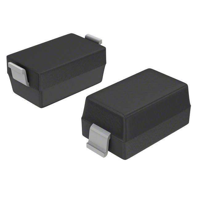
| 供应商器件封装 | 0603 |
| 其它名称 | CD0603-B00340DKR |
| 包装 | Digi-Reel® |
| 反向恢复时间(trr) | - |
| 商标 | Bourns |
| 安装类型 | 表面贴装 |
| 安装风格 | SMD/SMT |
| 封装 | Reel |
| 封装/外壳 | 0603(1608 公制) |
| 封装/箱体 | 0603 |
| 峰值反向电压 | 45 V |
| 工作温度-结 | -40°C ~ 125°C |
| 工作温度范围 | - 40 C to + 125 C |
| 工厂包装数量 | 4000 |
| 技术 | Silicon |
| 最大反向漏泄电流 | 1 uA at 40 V |
| 最大工作温度 | + 125 C |
| 最大浪涌电流 | 0.5 A |
| 最小工作温度 | - 40 C |
| 标准包装 | 1 |
| 正向电压下降 | 0.37 V at 0.001 A |
| 正向连续电流 | 30 mA |
| 热阻 | - |
| 电压-DC反向(Vr)(最大值) | 40V |
| 电流-平均整流(Io) | 30mA |
| 速度 | 小信号 =< 200mA(Io),任意速度 |
| 配置 | Single |

.jpg)


- 商务部:美国ITC正式对集成电路等产品启动337调查
- 曝三星4nm工艺存在良率问题 高通将骁龙8 Gen1或转产台积电
- 太阳诱电将投资9.5亿元在常州建新厂生产MLCC 预计2023年完工
- 英特尔发布欧洲新工厂建设计划 深化IDM 2.0 战略
- 台积电先进制程称霸业界 有大客户加持明年业绩稳了
- 达到5530亿美元!SIA预计今年全球半导体销售额将创下新高
- 英特尔拟将自动驾驶子公司Mobileye上市 估值或超500亿美元
- 三星加码芯片和SET,合并消费电子和移动部门,撤换高东真等 CEO
- 三星电子宣布重大人事变动 还合并消费电子和移动部门
- 海关总署:前11个月进口集成电路产品价值2.52万亿元 增长14.8%


PDF Datasheet 数据手册内容提取
NT Features This series is currently available, but not OMPLIA Lead free as standard r e M coomdeml eCnDd0e6d0 f3o-rB n0exwR Sdeersiiegsn sis. Tthhee HS C RoHS compliant* recommended replacement. Ro * Leadless S 3 Low stored charge CD0603/1005 Schottky Barrier Chip Diode Series General Information The markets of portable communications, computing and video equipment are challenging the semiconductor industry to develop increasingly smaller electronic components. Bourns offers small-signal high-speed Schottky Barrier Diodes for switching and rectification applications, in compact chip package 0603 and 1005 size format, which offer PCB real estate savings and are considerably smaller than most competitive parts. The Schottky Barrier Diodes offer a forward current of 30 mA, 100 mA or 200 mA, a reverse voltage of 30 V and 40 V and also have a low forward voltage option. The diodes are lead free with Cu/Ni/Au plated terminations and are compatible with lead free manufacturing processes, conforming to many industry and government regulations on lead free components. Bourns®Chip Diodes conform to JEDEC standards, easy to handle on standard pick and place equipment and their flat configuration makes roll away much more difficult. Electrical Characteristics (@ TA= 25 °C Unless Otherwise Noted) CDxxxx- CDxxxx- CDxxxx- CDxxxx- CDxxxx- CDxxxx- Parameter Symbol Unit B00340 B0130L B0140L B0140R B0230 B0240 0.37 0.44 0.55 0.45 0.50 0.55 Forward Voltage (Max.) VF (If= 1 mA) (If= 0.1 A) (If= 0.1 A) (If= 0.01 A) (If= 0.2 A) (If= 0.2 A) V Capacitance Between 1.5 9 9 9 12 12 (Tfe =rm 1i nMaHlsz ()Max.) CT (Vr= 1 V) (Vr= 10 V) (Vr= 10 V) (Vr= 10 V) (Vr= 10 V) (Vr= 10 V) pF 1 30 30 1 30 10 Reverse Current (Max.) IR (Vr= 40 V) (Vr= 30 V) (Vr= 10 V) (Vr= 10 V) (Vr= 30 V) (Vr= 30 V) µA How To Order CD 0603 - B 01 30 L Common Code Chip Diode Package • 0603 • 1005 Model B = Schottky Barrier Series Average Forward Current (Io) Code 003 = 30 mA 01 = 100 mA 02 = 200 mA (Code x 1000 mA = Average Forward Current) Reverse Voltage (VR) Code 30 = 30 V 40 = 40 V Forward Voltage Suffix L = Low Forward Voltage Vf(CDxxxx-B0130L) R = Low Reverse Current VR(CDxxxx-B0140R) *RoHS Directive 2002/95/EC Jan. 27, 2003 including annex and RoHS Recast 2011/65/EU June 8, 2011. Specifications are subject to change without notice. Users should verify actual device performance in their specific applications. The products described herein and this document are subject to specific disclaimers as set forth on the last page of this document, and at www.bourns.com/legal/disclaimer.pdf.
CD0603/1005 Schottky Barrier Chip Diode Series Absolute Ratings (@ TA= 25 °C Unless Otherwise Noted) CD0603- CD0603- CD0603- CD0603- CD0603- CD0603- Parameter Symbol Unit B00340 B0130L B0140L B0140R B0230 B0240 Repetitive Peak Reverse Voltage VRRM 45 35 45 45 35 45 V Reverse Voltage VR 40 30 40 40 30 40 V Average Forward Current Io 30 100 100 100 200 200 mA Forward Current, Surge Peak Isurge 500* 1000* 1000* 1000* 2000* 2000* mA Power Dissipation PD 150 mW Storage Temperature TSTG -40 to +125 °C Junction Temperature TJ -40 to +125 °C CD1005- CD1005- CD1005- CD1005- CD1005- CD1005- Parameter Symbol Unit B00340 B0130L B0140L B0140R B0230 B0240 Repetitive Peak Reverse Voltage VRRM 45 35 45 45 35 45 V Reverse Voltage VR 40 30 40 40 30 40 V Average Forward Current Io 30 100 100 100 200 200 mA Forward Current, Surge Peak Isurge 500* 1000* 1000* 1000* 3000* 3000* mA Power Dissipation PD 200 250 250 250 250 250 mW Storage Temperature TSTG -40 to +125 °C Junction Temperature TJ -40 to +125 °C * Condition: 8.3 ms single half sine-wave superimposed on rate load (JEDEC method). Specifications are subject to change without notice. Customers should verify actual device performance in their specific applications.
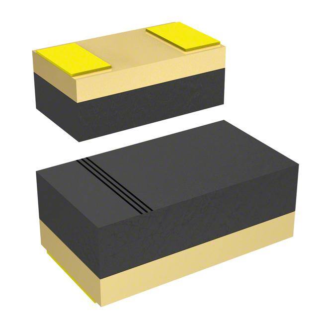
CD0603/1005 Schottky Barrier Chip Diode Series Product Dimensions Recommended Pad Layout A A B B C D Dimension 0603 1005 1.25 2.00 A (Max.) (0.049) (0.079) C B (Min.) 1.00 1.3 (0.039) (0.051) 0.6 0.7 C (Min.) (0.024) (0.028) MM DIMENSIONS: (INCHES) E Dimension 0603 1005 1.60 - 1.80 2.40 - 2.60 Physical Specifications A (0.063 - 0.071) (0.095 - 0.102) 0.80 - 1.00 1.10 - 1.30 Case....................................0603(1608) / 1005(2512) Molded plastic B (0.031 - 0.039) (0.043 - 0.051) Terminals..........................Gold plated, solderable per MIL-STD-750, 0.45 0.50 Method 2026 C Typ. Typ. (0.018) (0.020) Polarity ....................................................Indicated by cathode band 0.70 - 0.85 0.70 - 0.90 Mounting Position ........................................................................Any D (0.027 - 0.033) (0.027 - 0.035) Weight............................................0.000159 ounces / 0.0045 grams 0.70 1.00 E Typ. Typ. (0.028) (0.039) Typical Part Marking CDxxxx-B00340..............................................................................B2 MM DIMENSIONS: (INCHES) CDxxxx-B0130L..............................................................................B3 CDxxxx-B0140L..............................................................................B8 CDxxxx-B0140R..............................................................................B9 CDxxxx-B0230................................................................................B5 CDxxxx-B0240................................................................................B7 Specifications are subject to change without notice. Customers should verify actual device performance in their specific applications.
CD0603/1005 Schottky Barrier Chip Diode Series Rating and Characteristic Curves: CDxxxx-B00340 Forward Characteristics Reverse Characteristics 10 1000000 100000 125 °C 1 10000 ps) mAm nA) 85 °C Forward Current ( 0.1 Reverse Current ( 1000 100 125 °C 25 °C 85 °C 25 °C -25 °C 10 0.01 0 10 20 30 40 0.0 0.1 0.2 0.3 0.4 0.5 Reverse Voltage (Volts) Forward Voltage (Volts) Derating Curve Capacitance Between Terminals 120 16 Mounting on glass epoxy PCBs F = 1 MHz 14 Ta = 25 °C 100 nals (pF) 12 80 Termi 10 I Current (%)0 60 pacitance Between 86 40 Ca 4 20 2 0 0 0 5 10 15 20 25 30 0 25 50 75 100 125 150 Reverse Voltage (Volts) Ambient Temperature (°C) Specifications are subject to change without notice. Customers should verify actual device performance in their specific applications.
CD0603/1005 Schottky Barrier Chip Diode Series Rating and Characteristic Curves: CDxxxx-B0130L Forward Characteristics Reverse Characteristics 1000 1000000 100000 125 °C ps) 100 m mA 10000 Forward Current ( 10 Reverse Current (nA) 1000 85 °C 100 25 °C 125 °C 85 °C 25 °C -25 °C 1 0.0 0.1 0.2 0.3 0.4 0.5 0.6 10 0 5 10 15 20 25 30 Forward Voltage (Volts) Reverse Voltage (Volts) Derating Curve Capacitance Between Terminals 120 16 Mounting on glass epoxy PCBs 14 F = 1 MHz 100 Ta = 25 °C pF) 12 80 minals ( I Current (%)0 60 pacitance Between Ter 1806 40 Ca 4 20 2 0 0 0 5 10 15 20 25 30 0 25 50 75 100 125 150 Reverse Voltage (Volts) Ambient Temperature (°C) Specifications are subject to change without notice. Customers should verify actual device performance in their specific applications.
CD0603/1005 Schottky Barrier Chip Diode Series Rating and Characteristic Curves: CDxxxx-B0140L Forward Characteristics Reverse Characteristics 1000 10m 1m 75 °C 100u 100 A) urrent (mAmps) Reverse Current ( 110uu 25 °C C orward 10 100n -25 °C F 10n 125 °C 75 °C 25 °C -25 °C 1n 1 0 10 20 30 40 0.0 0.1 0.2 0.3 0.4 0.5 0.6 0.7 Reverse Voltage (Volts) Forward Voltage (Volts) Derating Curve Capacitance Between Terminals 120 20 F = 1 MHz Mounting on glass epoxy PCBs 18 Ta = 25 °C 100 16 pF) 80 minals ( 14 urrent (%) 60 Between Ter 1102 I C0 40 Capacitance 86 4 20 2 0 0 5 10 15 20 25 30 35 0 0 25 50 75 100 125 150 Reverse Voltage (Volts) Ambient Temperature (°C) Specifications are subject to change without notice. Customers should verify actual device performance in their specific applications.
CD0603/1005 Schottky Barrier Chip Diode Series Rating and Characteristic Curves: CDxxxx-B0140R Forward Characteristics Reverse Characteristics 1000 1m 125 °C 100u 100 10u 75 °C A) nt ( urrent (mAmps) 10 Reverse Curre 1u 25 °C C 100n d war For 1 10n -25 °C 75 °C -25 °C 125 °C 25 °C 1n 0.1 0 10 20 30 40 0.0 0.2 0.4 0.6 0.8 1.0 Reverse Voltage (Volts) Forward Voltage (Volts) Derating Curve Capacitance Between Terminals 120 20 F = 1 MHz Mounting on glass epoxy PCBs 18 Ta = 25 °C 100 16 pF) 80 minals ( 14 urrent (%) 60 Between Ter 1102 I C0 40 Capacitance 86 4 20 2 0 0 5 10 15 20 25 30 35 0 0 25 50 75 100 125 150 Reverse Voltage (Volts) Ambient Temperature (°C) Specifications are subject to change without notice. Customers should verify actual device performance in their specific applications.
CD0603/1005 Schottky Barrier Chip Diode Series Rating and Characteristic Curves: CDxxxx-B0230 Forward Characteristics Reverse Characteristics 1000 10000000 1000000 125 °C 100 A) 100000 n urrent (mAmps) Reverse Current ( 10000 85 °C C d war 10 1000 or F 25 °C 100 125 °C 85 °C 25 °C -25 °C 1 10 0.0 0.1 0.2 0.3 0.4 0.5 0 5 10 15 20 25 30 35 Forward Voltage (Volts) Reverse Voltage (Volts) Derating Curve Capacitance Between Terminals 120 100.0 Mounting on glass epoxy PCBs 90.0 F = 1 MHz Ta = 25 °C 100 80.0 80 nals (pF) 70.0 I Current (%)0 60 nce Between Termi 456000...000 40 pacita 30.0 Ca 20.0 20 10.0 0.0 0 0 5 10 15 20 25 30 35 0 25 50 75 100 125 150 Reverse Voltage (Volts) Ambient Temperature (°C) Specifications are subject to change without notice. Customers should verify actual device performance in their specific applications.
CD0603/1005 Schottky Barrier Chip Diode Series Rating and Characteristic Curves: CDxxxx-B0240 Forward Characteristics Reverse Characteristics 1000 10m 100 1m 125 °C 100u 10 A) 75 °C ward Current (mAmps) 0.11 125 °C75 °C Reverse Current ( 101010nuu 25 °C For 25 °C -25 °C 0.01 -25 °C 10n 1n 0.001 0 10 20 30 40 0.0 0.1 0.2 0.3 0.4 0.5 0.6 0.7 Forward Voltage (Volts) Reverse Voltage (Volts) Derating Curve Capacitance Between Terminals 120 100 Mounting on glass epoxy PCBs 90 F = 1 MHz 100 Ta = 25 °C 80 I Current (%)0 8600 nce Between Terminals (pF) 45670000 40 pacita 30 Ca 20 20 10 0 0 0 25 50 75 100 125 150 0 5 10 15 20 25 30 35 Ambient Temperature (°C) Reverse Voltage (Volts) Specifications are subject to change without notice. Customers should verify actual device performance in their specific applications.
CD0603/1005 Schottky Barrier Chip Diode Series Packaging Information The product will be dispensed in Tape and Reel format (see diagram below). P 0 P1 E T d Index Hole 120 ° F D2 W B D1 D P A C Trailer Device Leader ....... ....... ....... ....... W1 End ....... ....... ....... ....... Start MM DIMENSIONS: (INCHES) 10 pitches (min.) 10 pitches (min.) Devices are packed in accordance with EIA standard Direction of Feed RS-481-A and specifications shown here. Item Symbol 0603 1005 1.00 ±0.10 1.55 ±0.10 Carrier Width A (0.039 - 0.004) (0.061 - 0.004) 1.85 ±0.10 2.65 ±0.10 Carrier Length B (0.073 - 0.004) (0.104 - 0.004) 1.00 ±0.10 1.05 ±0.10 Carrier Depth C (0.039 - 0.004) (0.041 - 0.004) 1.55 ±0.05 1.55 ±0.10 Sprocket Hole d (0.061 - 0.002) (0.061 - 0.004) 178 178 Reel Outside Diameter D (7.008) (7.008) 60.0 60.0 Reel Inner Diameter D1 (2.362) MIN. (2.362) MIN. 13.0 ±0.20 13.0 ±0.20 Feed Hole Diameter D2 (0.512 - 0.008) (0.512 - 0.008) 1.75 ±0.10 1.75 ±0.10 Sprocket Hole Position E (0.069 - 0.004) (0.069 - 0.004) 3.50 ±0.05 3.50 ±0.05 Punch Hole Position F (0.138 - 0.002) (0.138 - 0.002) 4.00 ±0.10 4.00 ±0.10 Punch Hole Pitch P (0.157 - 0.004) (0.157 - 0.004) 4.00 ±0.10 4.00 ±0.10 Sprocket Hole Pitch P0 (0.157 - 0.004) (0.157 - 0.004) 2.00 ±0.05 2.00 ±0.05 Embossment Center P1 (0.079 - 0.002) (0.079 - 0.002) 0.20 ±0.05 0.25 ±0.05 Overall Tape Thickness T (0.008 - 0.002) (0.010 - 0.002) 8.00 ±0.20 8.00 ±0.20 Tape Width W (0.315 - 0.008) (0.315 - 0.008) 13.5 13.5 Reel Width W1 (0.531)MAX. (0.531)MAX. Quantity per Reel -- 4,000 4,000 REV. 10/17 Specifications are subject to change without notice. Customers should verify actual device performance in their specific applications.
Legal Disclaimer Notice This legal disclaimer applies to purchasers and users of Bourns® products manufactured by or on behalf of Bourns, Inc. and its affiliates (collectively, “Bourns”). Unless otherwise expressly indicated in writing, Bourns® products and data sheets relating thereto are subject to change without notice. Users should check for and obtain the latest relevant information before placing orders and should verify that such information is current and complete. The characteristics and parameters of a Bourns® product set forth in its data sheet are based on laboratory conditions, and statements regarding the suitability of products for certain types of applications are based on Bourns’ knowledge of typical requirements in generic applications. The characteristics and parameters of a Bourns® product in a user application may vary from the data sheet characteristics and parameters due to a combination of the Bourns® product with other components in the user’s application or due to the environment of the user application itself. Such characteristics and parameters also can and do vary in different applications and actual performance may vary over time. Users should always verify actual performance of the Bourns® product in their specific devices and applications, and make their own independent judgments about how much additional test margin to design in to compensate for differences between laboratory and real world conditions. Unless Bourns has explicitly designated an individual Bourns® product as meeting the requirements of a particular industry standard (e.g., ISO/TS 16949) or a particular qualification (e.g., UL listed or recognized), Bourns is not responsible for any failure of an individual Bourns® product to meet requirements of such industry standard or such particular qualification. Users of Bourns® products are responsible for ensuring compliance with safety-related requirements and standards applicable to their applications. Bourns® products are not recommended, authorized or intended for use in nuclear, lifesaving, life-critical or life-sustaining applications, nor in any other applications where failure or malfunction may result in personal injury, death, or severe property or environmental damage. Unless expressly and specifically approved in writing by two authorized Bourns representatives on a case-by-case basis, use of any Bourns® products in such unauthorized applications is at the user’s sole risk. Life-critical applications include devices identified by the U.S. Food and Drug Administration as Class III devices and generally equivalent classifications outside of the United States. Bourns® standard products that are designed and tested for use in automotive applications will be described on the applicable data sheets as compliant with the applicable AEC-Q standard. Unless expressly and specifically approved in writing by two authorized Bourns representatives on a case-by-case basis, use of any other Bourns® standard products in an automotive application is not recommended, authorized or intended and will be at the user’s sole risk. Bourns® standard products are not tested to comply with United States Federal Aviation Administration standards generally or any other generally equivalent governmental organization standard applicable to products designed or manufactured for use in aircraft or space applications. Bourns® standard products that are designed and tested for use in aircraft or space applications will be described on the applicable data sheets as compliant with the RTCA DO-160 standard. Unless expressly and specifically approved in writing by two authorized Bourns representatives on a case-by-case basis, use of any other Bourns® standard product in an aircraft or space application is not recommended, authorized or intended and will be at the user’s sole risk. The use and level of testing applicable to Bourns® custom products shall be negotiated on a case-by-case basis by Bourns and the user for which such Bourns® custom products are specially designed. Absent a written agreement between Bourns and the user regarding the use and level of such testing, the provisions above applicable to Bourns® standard products shall also apply to such Bourns® custom products. Users shall not sell, transfer, export or re-export any Bourns® products or technology for use in activities which involve the design, development, production, use or stockpiling of nuclear, chemical or biological weapons or missiles, nor shall they use Bourns® products or technology in any facility which engages in activities relating to such devices. The foregoing restrictions apply to all uses and applications that violate national or international prohibitions, including embargos or international regulations. Further, Bourns® products, technology or technical data may not under any circumstance be exported or re-exported to countries subject to international sanctions or embargoes, and Bourns® products may not, without prior authorization from Bourns and/or the U.S. Government, be resold, transferred, or re-exported to any party not eligible to receive U.S. commodities, software, and technical data. To the maximum extent permitted by applicable law, Bourns disclaims (i) any and all liability arising out of the application or use of any Bourns® standard product, (ii) any and all liability, including, without limitation, special, punitive, consequential or incidental damages, and (iii) any and all implied warranties, including implied warranties of fitness for particular purpose, non-infringement and merchantability. For your convenience, copies of this Legal Disclaimer Notice with German, Spanish, Japanese, Traditional Chinese and Simplified Chinese bilingual versions are available at: Web Page: http://www.bourns.com/legal/disclaimers-terms-and-policies PDF: http://www.bourns.com/docs/Legal/disclaimer.pdf C1753 10/18/17