
 Datasheet下载
- 型号: CAY10-104J4LF
- 制造商: Bourns
- 库位|库存: xxxx|xxxx
- 要求:
| 数量阶梯 | 香港交货 | 国内含税 |
| +xxxx | $xxxx | ¥xxxx |
查看当月历史价格
查看今年历史价格
CAY10-104J4LF产品简介:
ICGOO电子元器件商城为您提供CAY10-104J4LF由Bourns设计生产,在icgoo商城现货销售,并且可以通过原厂、代理商等渠道进行代购。 CAY10-104J4LF价格参考。BournsCAY10-104J4LF封装/规格:电阻器网络,阵列, 100k Ohm ±5% 62.5mW Power Per Element Isolated 4 Resistor Network/Array ±250ppm/°C 0804, Convex, Long Side Terminals。您可以下载CAY10-104J4LF参考资料、Datasheet数据手册功能说明书,资料中有CAY10-104J4LF 详细功能的应用电路图电压和使用方法及教程。
Bourns Inc.的CAY10-104J4LF是一款电阻器网络/阵列,常用于需要多个精密匹配电阻的电子电路中。该器件广泛应用于工业控制、通信设备、消费电子产品以及汽车电子等领域。其典型应用场景包括信号调节、电压分压、滤波电路、ADC/DAC接口匹配、传感器调理电路等。由于其高精度和良好的温度稳定性,CAY10-104J4LF也适用于要求较高的测试测量仪器和自动化设备中的精密模拟电路设计。
| 参数 | 数值 |
| 产品目录 | |
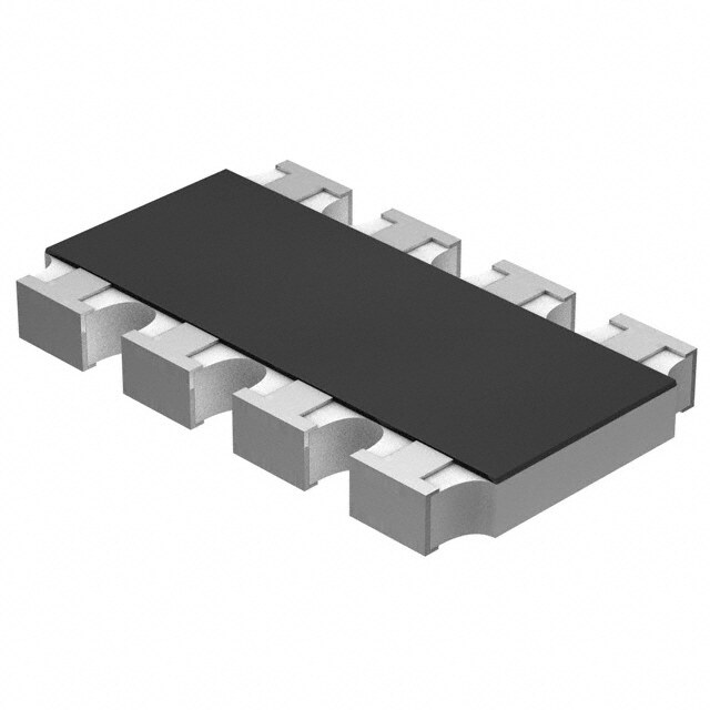
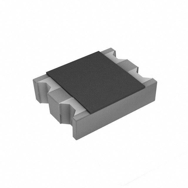
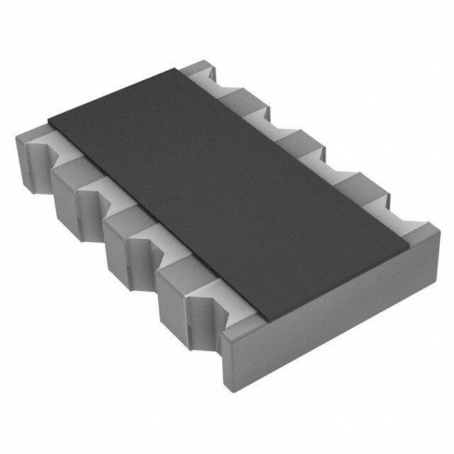
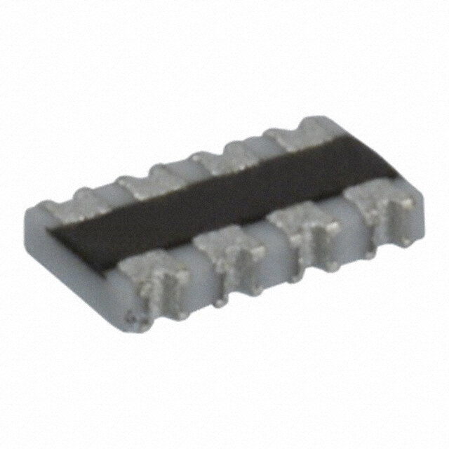
| 描述 | RES ARRAY 100K OHM 4 RES 0804电阻器网络与阵列 100K 5% Convex 4resistors |
| 产品分类 | |
| 品牌 | Bourns Inc. |
| 产品手册 | |
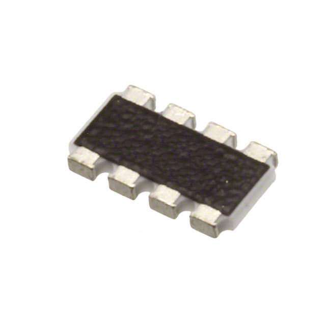
| 产品图片 |
|
| rohs | RoHS 合规性豁免无铅 / 符合限制有害物质指令(RoHS)规范要求 |
| 产品系列 | 电阻器网络与阵列,Bourns CAY10-104J4LFCAY10 |
| 数据手册 | |
| 产品型号 | CAY10-104J4LF |
| RoHS指令信息 | |
| 产品种类 | 电阻器网络与阵列 |
| 产品类型 | Arrays |
| 供应商器件封装 | - |
| 其它名称 | CAY10-104J4LFDKR |
| 包装 | Digi-Reel® |
| 商标 | Bourns |
| 外壳宽度 | 1 mm |
| 外壳长度 | 2 mm |
| 外壳高度 | 0.35 mm |
| 大小/尺寸 | 0.079" 长 x 0.039" 宽(2.00mm x 1.00mm) |
| 安装类型 | 表面贴装 |
| 容差 | ±5% |
| 封装 | Reel |
| 封装/外壳 | 0804,凸面,长边端子 |
| 工作温度 | -55°C ~ 125°C |
| 工作温度范围 | - 55 C to + 125 C |
| 工厂包装数量 | 10000 |
| 应用 | - |
| 引脚数 | 8 |
| 标准包装 | 1 |
| 每元件功率 | 62.5mW |
| 温度系数 | ±250ppm/°C |
| 电路类型 | 隔离 |
| 电阻(Ω) | 100k |
| 电阻器数 | 4 |
| 电阻器数量 | 4 |
| 电阻数值 | 100 kOhms |
| 端接类型 | SMD/SMT |
| 系列 | CAY10 |
| 高度 | 0.018"(0.45mm) |

.jpg)


PDF Datasheet 数据手册内容提取
Features n RoHS compliant* n Paper tape on reel for automatic placement n 2/4 isolated resistors in an 0404/0804 size package n E24 series from 10 ohms to 1 megohm n Convex termination style n Resistance tolerance ±5 % n Suitable for all types of soldering processes Model CAY10 - Chip Resistor Array Specifications Requirement Characteristics Test Method Short Time Overload ±2 % Rated Voltage X 2.5, 5 seconds Soldering Heat ±1 % 260 °C ±5 °C, 10 seconds ±1 second Temperature Cycling (5) ±1 % 125 °C (30 minutes) - normal (15 minutes) -30 °C (30 minutes) - normal (15 minutes) Moisture Load Life ±3 % 1000 hours Load Life ±3 % 1000 hours Characteristics How To Order CA Y 10 - 103 J 4 LF Characteristics CAY10-xxxJ2 CAY10-xxxJ4 Chip Arrays Number of Elements (Isolated) 2 4 Type • Y = Convex Power Rating @ 70 °C per Resistor 0.0625 W 0.0625 W Model • 10 = 04 Package Width Package Power Rating @ 70 °C 0.125 W 0.250 W Resistance Code • <10 ohms: “R” represents decimal Resistance Tolerance ±5 % point (example: 4R7 = 4.7 ohms). • ≥10 ohms: First two digits are signifi- Resistance Range (E24) 3 ohms - 1 megohm cant, third digit represents number of plus Zero-ohm Jumper zeros to follow (example: 474 = 470k ohms 3 ohms ~ 9.1 ohms: ±500 ppm/°C T.C.R. • 000 = Zero-ohm Jumper 10 ohms ~ 1 megohm: ±200 ppm/°C Resistance Tolerance • J = ±5 % Max. Overload Voltage 50 V Resistors Max. Working Voltage 25 V • 2 = 2 Resistors • 4 = 4 Resistors Operating Temp. Range -55 °C to +125 °C Terminations • LF = Tin-plated (RoHS compliant) Rating Temperature +70 °C For Standard Values Used in Capacitors, Packaging 10,000 pieces per reel Inductors, and Resistors, click here. Characteristics Derating Curve Environmental Characteristics Protective 70 ϒC 125 ϒC 100 Moisture Sensitivity Level .........................1 Glass Overcoat Thick Film %) 80(cid:31) ESD Classification (HBM) .....................N/A Resistive Element d ( 60 a ed Lo 2400 Isolated Circuit Rat 0 CAY10-xxxJ2 44 33 -55 40 60 80 100 120 140 160 Ambient Temp. (˚C) RR RR Typical Part Marking Termination 11 22 High Purity Alumina None on part. Label on reel will include Substrate part number. CAY10-xxxJ4 88 77 66 55 RR RR RR RR 11 22 33 44 WARNING Cancer and Reproductive Harm - www.P65Warnings.ca.gov *RoHS Directive 2015/863, Mar 31, 2015 and Annex. Specifications are subject to change without notice. Users should verify actual device performance in their specific applications. The products described herein and this document are subject to specific legal disclaimers as set forth on the last page of this document, and at www.bourns.com/docs/legal/disclaimer.pdf.
Model CAY10 - Chip Resistor Array Soldering Profile for RoHS Compliant Chip Resistors and Arrays 275 <1>Maximum of 20 seconds between 260 °C peak +255 °C and +260 °C < 1 > 255 °C 225 220 °C C) e (° 190 °C s6e0c o- n9d0s ur 175 at 150 °C Ramp Down er 6 °C/second p m e T 125 60 - 120 seconds 0.40 ± 0.15 0.40 ± 0.15 (.016 ± .006) (.016 ± .006) 10 seconds minimum 75 R3 a°mC/ps eUcpond maximum (.00.0165 ±± .00.0140) (.104.00 ± ± 0.0.1004) (.00.1205 ±± .00.0140) (.10.400 ± ± 0.0.1004) (.000.728 ± ± 0 ..01004) 0.2 ± 0.10 (.0078 ± .004) 25 0 50 100 150 200 250 300 Time (Seconds)0.5 ± 0.05 0.30 ± 0.15 0.35 ± 0.10 0.5 ± 0.05 0.30 ± 0.15 0.35 ± 0.10 (.020 ± .002) (.012 ± .006) (.014 ± .004) (.020 ± .002) (.012 ± .006) (.014 ± .004) 2.0 ± 0.10 2.0 ± 0.10 (.079 ± .004) (.079 ± .004) Product Dimensions 0.50 0.50 CAY10-xxxJ4 CAY10-xx(.x02J02) (.020) 0.40 ± 0.15 0.40 ± 0.15 00.5.303 ± 0.10 0.33 ± 0.10 (.016 ± .006) (.016 ± .006) (.(0.02103) ± .004) (.013 ± .004) 1.50 (.059) 0.15 ± 0.10 0.25 ± 0.10 0.15 ± 0.10 0.250 .±2 0±. 100.10 0.2 ± 0.15 0.25 ± 0.10 (.006 ± .004) 1.0 ± 0.10 (.010 ± .004) (.006 ± .004) 1.0 ± 0.101.0 ± 0.10 (.0(1.000 ±7 8.0 ±0 4.0) 04) (.0078 ± .006) 1.0 ± 0.20 (.010 ± .004) (.040 ±.004) (.040 ±.00(4.0)4 0 ±.004) (.040 ±.008) 0.2 ± 0.10 (.0078 ± .004) 0.40 0.30 (.016) (.012) 0.5 ± 0.05 0.30 ± 0.15 0.35 ± 0.10 0.5 ± 0.05 0.67 ± 0.10 0.30 ± 0.15 0.305. 3±5 0 ±.1 00.10 0.65 ± 0.10 0.35 ± 0.10 (.020 ± .002) (.012 ± .006) (.014 ± .004) (.020 ± .002) (.026 ± .004) (.012 ± .006) (.01(.40 1±4 . 0±0 .40)0 4) (.025 ± .004) (.014 ± .004) 2.0 ± 0.10 2.10. 0± ±0 .01.010 1.0 ± 0.20 (.079 ± .004) (.0(.7094 0± ±.0 .0040)4 ) (.040 ± .008) Land Pattern 0.33 ± 0.10 0.33 ± 0.10 CAY10-xxx(J.0413 ± .004) (.013 ± .004) CAY10-xxxJ2 0.50 0.50 0.65 (.020) (.020) (.026) 0.15 ± 0.10 0.25 ± 0.10 0.2 ± 0.15 0.25 ± 0.10 DIMENSIONS: MM (.006 ± .(0.000.2450)0 ) (.10.400 ± ± 0.0.1004) (.010 ± .004) (.0078 ± .006) ((.0.010.254.0000 )± ± 0.0.2008) (.010 ± .004) (INCHES) 1.50 1.50 (.059) (.059) 0.67 ± 0.10 0.35 ± 0.10 0.65 ± 0.10 0.35 ± 0.10 (.026 ± .004) (.014 ± .004) (.025 ± .004) (.014 ± .004) 1.0 ± 0.10 1.0 ± 0.20 (.040 ± .004) (.040 ± .008) 0.40 0.30 0.35 MM (.016) (.012) DIMENSIONS: (.014) (INCHES) Specifications are subject to change without notice. Users should verify actual device performance in their specific applications. The products described herein and this document are subject to specific legal disclaimers as set forth on the last page of this document, and at www.bourns.com/docs/legal/disclaimer.pdf. 0.65 (.026) 0.50 (.020) 1.50 (.059) 0.35 (.014)
Model CAY10 - Chip Resistor Array Packaging Dimensions (.00.1485 ±± ..000140) MAX. (.10.5590D +I±A ...000140) (.41.5070 ±± .00.0140) (.10.6795 ±± .00.0140) (.027.90 ±± .00.250) 13.0 ± 0.2 (.511 ± .008) CAY10-xxxJ2:(.10.4270 ±± .00.0140) 3.50 ± 0.05 60 (.138 ± .002) (2.362) 8.00 ± 0.20 (.315 ± .008) CAY10-xxxJ4: 2.20 ± 0.10 9.0 ± 0.3 (.087 ± .004) 21.0 ± 0.8 (.354 ± .012) (.014.00) MAX. (.10.4270 ±± .00.0140) (.20.7090 ±± .00.0140) (71.08807) (.827 ± .031) (.41419.4 ± ± . 014.00) MM DIMENSIONS: (INCHES) REV. 07/20 Specifications are subject to change without notice. Users should verify actual device performance in their specific applications. The products described herein and this document are subject to specific legal disclaimers as set forth on the last page of this document, and at www.bourns.com/docs/legal/disclaimer.pdf.
Legal Disclaimer Notice This legal disclaimer applies to purchasers and users of Bourns® products manufactured by or on behalf of Bourns, Inc. and its affiliates (collectively, “Bourns”). Unless otherwise expressly indicated in writing, Bourns® products and data sheets relating thereto are subject to change without notice. Users should check for and obtain the latest relevant information and verify that such information is current and complete before placing orders for Bourns® products. The characteristics and parameters of a Bourns® product set forth in its data sheet are based on laboratory conditions, and statements regarding the suitability of products for certain types of applications are based on Bourns’ knowledge of typical requirements in generic applications. The characteristics and parameters of a Bourns® product in a user application may vary from the data sheet characteristics and parameters due to (i) the combination of the Bourns® product with other components in the user’s application, or (ii) the environment of the user application itself. The characteristics and parameters of a Bourns® product also can and do vary in different applications and actual performance may vary over time. Users should always verify the actual performance of the Bourns® product in their specific devices and applications, and make their own independent judgments regarding the amount of additional test margin to design into their device or application to compensate for differences between laboratory and real world conditions. Unless Bourns has explicitly designated an individual Bourns® product as meeting the requirements of a particular industry standard (e.g., ISO/TS 16949) or a particular qualification (e.g., UL listed or recognized), Bourns is not responsible for any failure of an individual Bourns® product to meet the requirements of such industry standard or particular qualification. Users of Bourns® products are responsible for ensuring compliance with safety-related requirements and standards applicable to their devices or applications. Bourns® products are not recommended, authorized or intended for use in nuclear, lifesaving, life-critical or life-sustaining ap- plications, nor in any other applications where failure or malfunction may result in personal injury, death, or severe property or environmental damage. Unless expressly and specifically approved in writing by two authorized Bourns representatives on a case-by-case basis, use of any Bourns® products in such unauthorized applications might not be safe and thus is at the user’s sole risk. Life-critical applications include devices identified by the U.S. Food and Drug Administration as Class III devices and generally equivalent classifications outside of the United States. Bourns expressly identifies those Bourns® standard products that are suitable for use in automotive applications on such products’ data sheets in the section entitled “Applications.” Unless expressly and specifically approved in writing by two authorized Bourns representatives on a case-by-case basis, use of any other Bourns® standard products in an automotive application might not be safe and thus is not recommended, authorized or intended and is at the user’s sole risk. If Bourns expressly identifies a sub-category of automotive application in the data sheet for its standard products (such as infotainment or lighting), such identification means that Bourns has reviewed its standard product and has determined that if such Bourns® standard product is considered for potential use in automotive applications, it should only be used in such sub-category of automotive applications. Any reference to Bourns® standard product in the data sheet as compliant with the AEC-Q standard or “automotive grade” does not by itself mean that Bourns has approved such product for use in an automotive application. Bourns® standard products are not tested to comply with United States Federal Aviation Administration standards generally or any other generally equivalent governmental organization standard applicable to products designed or manufactured for use in aircraft or space applications. Bourns expressly identifies Bourns® standard products that are suitable for use in aircraft or space applications on such products’ data sheets in the section entitled “Applications.” Unless expressly and specifically approved in writing by two authorized Bourns representatives on a case-by-case basis, use of any other Bourns® standard product in an aircraft or space application might not be safe and thus is not recommended, authorized or intended and is at the user’s sole risk. The use and level of testing applicable to Bourns® custom products shall be negotiated on a case-by-case basis by Bourns and the user for which such Bourns® custom products are specially designed. Absent a written agreement between Bourns and the user regarding the use and level of such testing, the above provisions applicable to Bourns® standard products shall also apply to such Bourns® custom products. Users shall not sell, transfer, export or re-export any Bourns® products or technology for use in activities which involve the design, development, production, use or stockpiling of nuclear, chemical or biological weapons or missiles, nor shall they use Bourns® products or technology in any facility which engages in activities relating to such devices. The foregoing restrictions apply to all uses and applications that violate national or international prohibitions, including embargos or international regulations. Further, Bourns® products and Bourns technology and technical data may not under any circumstance be exported or re-exported to countries subject to international sanctions or embargoes. Bourns® products may not, without prior authorization from Bourns and/or the U.S. Government, be resold, transferred, or re-exported to any party not eligible to receive U.S. commodities, software, and technical data. To the maximum extent permitted by applicable law, Bourns disclaims (i) any and all liability for special, punitive, consequential, incidental or indirect damages or lost revenues or lost profits, and (ii) any and all implied warranties, including implied warranties of fitness for particular purpose, non-infringement and merchantability. For your convenience, copies of this Legal Disclaimer Notice with German, Spanish, Japanese, Traditional Chinese and Simplified Chinese bilingual versions are available at: Web Page: http://www.bourns.com/legal/disclaimers-terms-and-policies PDF: http://www.bourns.com/docs/Legal/disclaimer.pdf C1753 05/17/18R