ICGOO在线商城 > 集成电路(IC) > PMIC - 监控器 > CAT809STBI-GT3

 Datasheet下载
- 型号: CAT809STBI-GT3
- 制造商: ON Semiconductor
- 库位|库存: xxxx|xxxx
- 要求:
| 数量阶梯 | 香港交货 | 国内含税 |
| +xxxx | $xxxx | ¥xxxx |
查看当月历史价格
查看今年历史价格
CAT809STBI-GT3产品简介:
ICGOO电子元器件商城为您提供CAT809STBI-GT3由ON Semiconductor设计生产,在icgoo商城现货销售,并且可以通过原厂、代理商等渠道进行代购。 CAT809STBI-GT3价格参考。ON SemiconductorCAT809STBI-GT3封装/规格:PMIC - 监控器, 推挽式,图腾柱 监控器 1 通道 SOT-23-3。您可以下载CAT809STBI-GT3参考资料、Datasheet数据手册功能说明书,资料中有CAT809STBI-GT3 详细功能的应用电路图电压和使用方法及教程。
CAT809STBI-GT3 是安森美(ON Semiconductor)推出的一款电源管理集成电路(PMIC),属于监控器类别。其主要应用场景包括但不限于以下几类:

1. 电池供电设备:CAT809STBI-GT3 可用于便携式电子设备中,例如手持终端、无线传感器节点和智能家居控制器等。它能够监测电池电压状态,并提供低功耗模式支持,延长设备续航时间。

2. 工业自动化系统:在工业控制领域,该芯片可用于监控关键电路的电源状态,确保系统的稳定运行。例如,在PLC模块或数据采集单元中,CAT809STBI-GT3可以检测输入电压是否正常,并在异常情况下触发保护机制。

3. 消费类电子产品:适用于各种需要精确电压监测的消费类产品,如可穿戴设备、数码相机和个人健康监测仪等。通过设定不同的阈值电压点,CAT809STBI-GT3可以帮助这些设备实现更高效的电源管理和用户提示功能。

4. 通信设备:在网络路由器、调制解调器或其他通信基础设施中,此监控器可用于保障核心组件的供电安全,防止因电压波动导致的数据丢失或硬件损坏。

5. 汽车电子系统:尽管CAT809STBI-GT3并非专门针对汽车级应用设计,但在某些非关键任务场景下(如车内娱乐系统或环境照明控制),它仍然可以发挥作用,用于监测辅助电源线路的状态。

总之,CAT809STBI-GT3凭借其简单易用的设计和可靠的性能表现,广泛应用于各类需要实时电压监控及故障报告的场合,帮助提高整个系统的可靠性和安全性。
| 参数 | 数值 |
| 产品目录 | 集成电路 (IC)半导体 |
| 描述 | IC SUPERVISOR PP ACT LOW SOT-23监控电路 Push-pull Act low |
| 产品分类 | |
| 品牌 | ON Semiconductor |
| 产品手册 | |
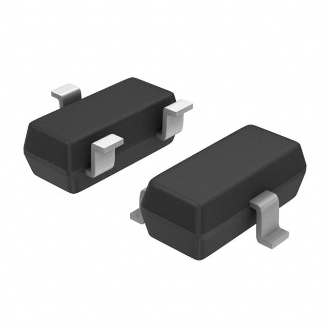
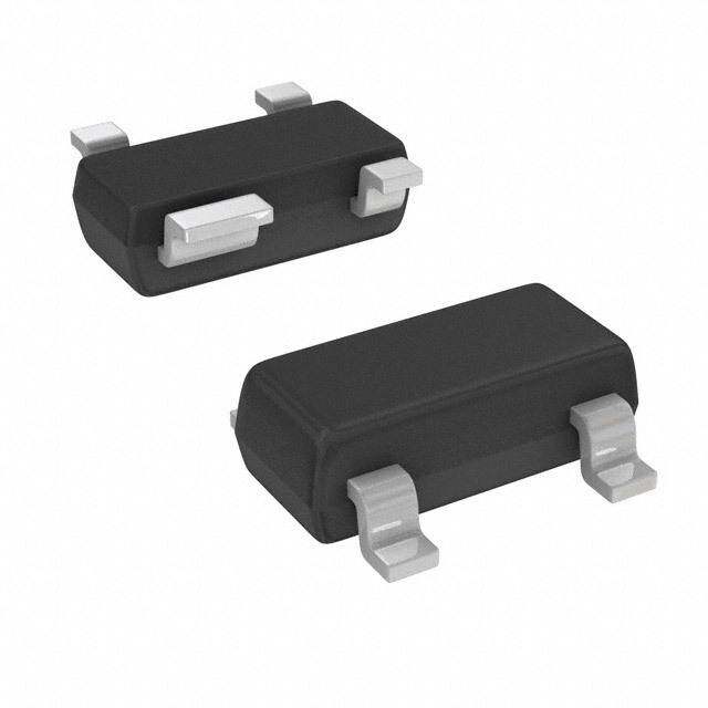
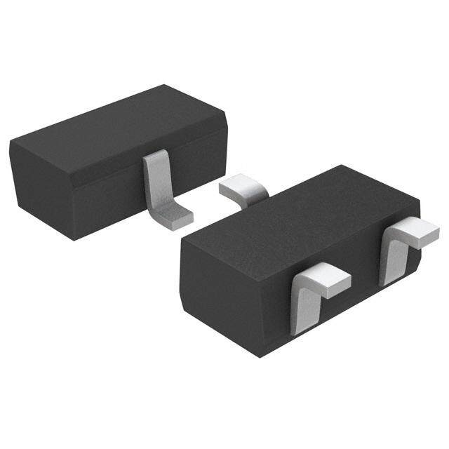
| 产品图片 |
|
| rohs | 符合RoHS无铅 / 符合限制有害物质指令(RoHS)规范要求 |
| 产品系列 | 电源管理 IC,监控电路,ON Semiconductor CAT809STBI-GT3- |
| NumberofInputsMonitored | 1 Input |
| 数据手册 | |
| 产品型号 | CAT809STBI-GT3 |
| 产品种类 | 监控电路 |
| 人工复位 | No Manual Reset |
| 供应商器件封装 | SOT-23-3 |
| 其它名称 | CAT809STBI-GT3OSDKR |
| 功率失效检测 | No |
| 包装 | Digi-Reel® |
| 受监控电压数 | 1 |
| 商标 | ON Semiconductor |
| 复位 | 低有效 |
| 复位超时 | 最小为 140 ms |
| 安装类型 | 表面贴装 |
| 安装风格 | SMD/SMT |
| 封装 | Reel |
| 封装/外壳 | TO-236-3,SC-59,SOT-23-3 |
| 封装/箱体 | SOT-23-3 |
| 工作温度 | -40°C ~ 85°C |
| 工作电源电流 | 15 uA |
| 工厂包装数量 | 3000 |
| 最大功率耗散 | 320 mW |
| 最大工作温度 | + 85 C |
| 最小工作温度 | - 40 C |
| 标准包装 | 1 |
| 欠电压阈值 | 2.89 V |
| 电压-阈值 | 2.93V |
| 电池备用开关 | No Backup |
| 电源电压-最大 | 5.5 V |
| 电源电压-最小 | 1.2 V |
| 监视器 | No Watchdog |
| 类型 | 简单复位/加电复位 |
| 系列 | CAT809 |
| 芯片启用信号 | No Chip Enable |
| 被监测输入数 | 1 Input |
| 输出 | 推挽式,图腾柱 |
| 输出类型 | Active Low, Push-Pull |
| 过电压阈值 | 2.96 V |
| 重置延迟时间 | 240 ms |
| 阈值电压 | 2.5 V, 3 V, 3.3 V, 5 V |


- 商务部:美国ITC正式对集成电路等产品启动337调查
- 曝三星4nm工艺存在良率问题 高通将骁龙8 Gen1或转产台积电
- 太阳诱电将投资9.5亿元在常州建新厂生产MLCC 预计2023年完工
- 英特尔发布欧洲新工厂建设计划 深化IDM 2.0 战略
- 台积电先进制程称霸业界 有大客户加持明年业绩稳了
- 达到5530亿美元!SIA预计今年全球半导体销售额将创下新高
- 英特尔拟将自动驾驶子公司Mobileye上市 估值或超500亿美元
- 三星加码芯片和SET,合并消费电子和移动部门,撤换高东真等 CEO
- 三星电子宣布重大人事变动 还合并消费电子和移动部门
- 海关总署:前11个月进口集成电路产品价值2.52万亿元 增长14.8%


PDF Datasheet 数据手册内容提取
CAT803, CAT809, CAT810 3-Pin Microprocessor Power Supply Supervisors Description The CAT803, CAT809, and CAT810 are supervisory circuits that monitor power supplies in digital systems. The CAT803, CAT809, and http://onsemi.com CAT810 are direct replacements for the MAX803, MAX809 and MAX810 in applications operating over the industrial temperature range. These devices generate a reset signal, which is asserted while the power supply voltage is below a preset threshold level and for at least 140ms after the power supply level has risen above that level. The underlying floating gate technology, Analog EEPROM used by SOT−23 ONSemiconductor, makes it possible to offer any custom reset TB SUFFIX threshold value. Seven industry standard threshold levels are offered CASE 527AG to support +5.0V, +3.3V, +3.0V and +2.5V systems. The CAT803 has an open−drain RESET output (active LOW). The CAT803 requires a pull−up resistor on the reset output. The CAT809 features a push−pull RESET output (active LOW) and the CAT810 features a push−pull RESET output (active HIGH). SC−70 SD SUFFIX Fast transients on the power supply are ignored and the output is CASE 419AB guaranteed to be in the correct state at V levels as low as 1.0 V. CC The CAT803, CAT809, and CAT810 are available in both the compact 3−pin SOT−23 and SC−70 packages. PIN CONFIGURATION Features 1 3−Lead SOT23 • GND 3−Lead SC70 Precision Monitoring of 3 +5.0 V (−5%, −10%, −20%), VCC +3.3 V (−5%, −10%), 2 CAT803 +3.0 V (−10%) and RESET CAT809 +2.5 V (−5%) Power Supplies (RESET) (CAT810) • (Top View) Offered in Three Output Configurations: − CAT803: Open−Drain Active LOW Reset − CAT809: Push−Pull Active LOW Reset MARKING DIAGRAMS − CAT810: Push−Pull Active HIGH Reset • Direct Replacements for the MAX803, MAX809 and MAX810 in XXXM(cid:2) XXXM(cid:2) Applications Operating over the Industrial Temperature Range (cid:2) (cid:2) • Reset Valid down to V = 1.0 V CC • 6 (cid:2)A Power Supply Current • SOT−23 SC−70 Power Supply Transient Immunity • Industrial Temperature Range: −40°C to +85°C XXX = Specific Device Code • M = Month Code Available in SOT−23 and SC−70 Packages (cid:2) = Pb−Free Package • These Devices are Pb−Free and are RoHS Compliant (*Note: Microdot may be in either location) Applications • Computers, Servers, Laptops, Cable Modems ORDERING INFORMATION • Wireless Communications See detailed ordering and shipping information in the package • dimensions section on page 8 of this data sheet. Embedded Control Systems • White Goods, Power Meters • Intelligent Instruments • PDAs and Handheld Equipment © Semiconductor Components Industries, LLC, 2012 1 Publication Order Number: October, 2012 − Rev. 33 CAT803/D
CAT803, CAT809, CAT810 Table 1. THRESHOLD SUFFIX SELECTOR Nominal Threshold Voltage Threshold Suffix Designation 4.63 V L 4.55 V H 4.38 V M 4.00 V J 3.08 V T 2.93 V S 2.63 V R 2.32 V Z 1.60 V V Table 2. PIN DESCRIPTIONS Pin Number CAT803 CAT809 CAT810 Name Description 1 1 1 GND Ground 2 2 − RESET Active LOW reset. RESET is asserted if VCC falls below the reset threshold and remains low for at least 140 ms after VCC rises above the reset threshold. − − 2 RESET Active HIGH reset. RESET is asserted if VCC falls below the reset threshold and remains high for at least 140 ms after VCC rises above the reset threshold. 3 3 3 VCC Power supply voltage that is monitored. Table 3. ABSOLUTE MAXIMUM RATINGS Parameter Rating Units Any pin with respect to ground −0.3 to +6.0 V Input Current, VCC 20 mA Output Current, RESET, RESET 20 mA Rate of Rise, VCC 100 V/(cid:2)s Continuous Power Dissipation mW Derate 2.2 mW/°C above 70°C (SC70) 175 Derate 4 mW/°C above 70°C (SOT23) 320 Operating Temperature Range −40 to +85 °C Storage Temperature Range −65 to +105 °C Lead Soldering Temperature (10 sec) 300 °C Stresses exceeding Maximum Ratings may damage the device. Maximum Ratings are stress ratings only. Functional operation above the Recommended Operating Conditions is not implied. Extended exposure to stresses above the Recommended Operating Conditions may affect device reliability. http://onsemi.com 2
CAT803, CAT809, CAT810 VCC VCC VCC TOLBEIRAASNCE + DIGITAL RESET DELAY – VOLTAGE REFERENCE CAT803 GND VCC VCC VCC TOLERANCE + BIAS DIGITAL RESET – DELAY VOLTAGE REFERENCE CAT809 GND VCC VCC VCC TOLBEIRAASNCE + DIGITAL RESET – DELAY VOLTAGE REFERENCE CAT810 GND Figure 1. Block Diagrams http://onsemi.com 3
CAT803, CAT809, CAT810 Table 4. ELECTRICAL CHARACTERISTICS (VCC = Full range, TA = −40°C to +85°C, unless otherwise specified. Typical values at TA = +25°C and VCC = 5 V for the L/H/M/J versions, VCC = 3.3 V for the T/S versions, VCC = 3 V for the R version and VCC = 2.5 V for the Z/V versions.) Typ Symbol Parameter Conditions Min (Note 1) Max Units VCC Range TA = 0°C to +70°C 1.0 5.5 V TA = −40°C to +85°C 1.2 5.5 ICC Supply Current TA = −40°C VCC < 5.5 V, J/L/M/H 8 20 (cid:2)A to +85°C VCC < 3.6 V, R/S/T/Z/V 6 15 VTH Reset Threshold Voltage L Threshold TA = +25°C 4.56 4.63 4.70 V TA = −40°C to +85°C 4.50 4.75 H Threshold TA = +25°C 4.48 4.55 4.62 TA = −40°C to +85°C 4.43 4.67 M Threshold TA = +25°C 4.31 4.38 4.45 TA = −40°C to +85°C 4.25 4.50 J Threshold TA = +25°C 3.93 4.00 4.06 TA = −40°C to +85°C 3.89 4.10 T Threshold TA = +25°C 3.04 3.08 3.11 TA = −40°C to +85°C 3.00 3.15 S Threshold TA = +25°C 2.89 2.93 2.96 TA = −40°C to +85°C 2.85 3.00 R Threshold TA = +25°C 2.59 2.63 2.66 TA = −40°C to +85°C 2.55 2.70 Z Threshold TA = +25°C 2.28 2.32 2.35 TA = −40°C to +85°C 2.25 2.38 V Threshold TA = +25°C 1.58 1.60 1.62 TA = −40°C to +85°C 1.56 1.64 Reset Threshold Tempco 30 ppm/°C TD VCC to Reset Delay (Note 2) VCC = VTH to (VTH − 100 mV) 20 (cid:2)s TR Reset Active Timeout Period TA = −40°C to +85°C 140 240 460 ms VOL RESET Output Voltage Low VCC = VTH min, ISINK = 1.2 mA 0.3 V (Open−drain active LOW, CAT803R/S/T/Z, CAT809R/S/T/Z/V CAT803 and push−pull, active LOW, CAT809) VCC = VTH min, ISINK = 3.2 mA 0.4 CAT803J/L/M, CAT809J/L/M/H VCC > 1.0 V, ISINK = 50 (cid:2)A 0.3 VOH RESET Output Voltage High VCC = VTH max, ISOURCE = 500 (cid:2)A 0.8 VCC V (Push−pull, active LOW, CAT809R/S/T/Z/V CAT809) VCC = VTH max, ISOURCE = 800 (cid:2)A VCC − 1.5 CAT809J/L/M/H VOL RESET Output Voltage Low VCC > VTH max, ISINK = 1.2 mA 0.3 V (Push−pull, active HIGH, CAT810R/S/T/Z CAT810) VCC > VTH max, ISINK = 3.2 mA 0.4 CAT810J/L/M VOH RESET Output Voltage High 1.8 V < VCC VTH min, 0.8 VCC V (Push−pull, active HIGH, ISOURCE = 150 (cid:2)A CAT810) 1. Production testing done at TA = +25°C; limits over temperature guaranteed by design only. 2. RESET output for the CAT809; RESET output for the CAT810. http://onsemi.com 4
CAT803, CAT809, CAT810 TYPICAL OPERATING CHARACTERISTICS (VCC = Full range, TA = −40°C to +85°C, unless otherwise specified. Typical values at TA = +25°C and VCC = 5 V for the L/M/J versions, VCC = 3.3 V for the T/S versions, VCC = 3 V for the R version and VCC = 2.5 V for the Z version.) 260 12 S) m OUT ( 240 VCC = 5 V (cid:2)A) 10 VCC = 5.5 V E T ( 8 M N TI 220 E ET RR 6 VCC = 3.6 V ES VCC = 2.5 V CU R 200 Y UP PPL 4 R− U WE 180 S 2 O P 160 0 −50 0 50 100 150 −50 0 50 100 150 TEMPERATURE (°C) TEMPERATURE (°C) Figure 2. Power−up Reset Timeout vs. Figure 3. Supply Current vs. Temperature Temperature (No Load, CAT8xxR/S/T/Z) 14 1.0002 S) (cid:2) Y ( 12 D1.0000 A L L O E 10 H0.9998 D S SET 8 HRE0.9996 E T R D N 6 E0.9994 OW ALIZ D 4 M0.9992 R− R E O W 2 N0.9990 O P 0 0.9988 −50 0 50 100 150 0 20 40 60 80 100 120 TEMPERATURE (°C) TEMPERATURE (°C) Figure 4. Power−down Reset Delay vs. Figure 5. Normalized Reset Threshold vs. Temperature (CAT8xxR/S/T/Z) Temperature http://onsemi.com 5
CAT803, CAT809, CAT810 Detailed Descriptions Reset Timing The reset signal is asserted LOW for the CAT803/CAT809 and HIGH for the CAT810 when the power supply voltage falls below the threshold trip voltage and remains asserted for at least 140 ms after the power supply voltage has risen above the threshold. 5 V VTH VCC 0 V TD TR Reset Timeout Period (140 ms minimum) 5 V CAT803, CAT809 RESET 0 V 5 V CAT810 RESET 0 V Figure 6. Reset Timing Diagram V Transient Response 30 CC The CAT803/CAT809/CAT810 protect (cid:2)Ps against TAMB = 25°C brownout failure. Short duration transients of 4 (cid:2)sec or less s) 25 (cid:2) and 100 mV amplitude typically do not cause a false RESET. N ( Figure 7 shows the maximum pulse duration of negative− O 20 TI going VCC transients that do not cause a reset condition. RA U As the amplitude of the transient goes further below the D 15 threshold (increasing V − V ), the maximum pulse T CAT809Z TH CC N duration decreases. In this test, the VCC starts from an initial SIE 10 voltage of 0.5 V above the threshold and drops below it by N CAT809M A the amplitude of the overdrive voltage (VTH − VCC). TR 5 0 1 10 100 1000 RESET OVERDRIVE VTH − VCC (mV) Figure 7. Maximum Transient Duration without Causing a Reset Pulse vs. Reset Comparator Overdrive http://onsemi.com 6
CAT803, CAT809, CAT810 Valid RESET with V Under 1.0 V CC To ensure that the CAT809 RESET pin is in a known state when V is under 1.0 V, a >10 k(cid:3) pull−down resistor between CC RESET pin and GND is recommended. For the CAT810, a pull−up resistor from RESET pin to V is needed. CC Power Power Supply Supply VCC VCC 10 k(cid:3) CAT810 CAT809 RESET RESET GND 10 k(cid:3) GND Figure 8. RESET Valid with V Under 1.0 V Figure 9. RESET Valid with V Under 1.1 V CC CC Bi−directional Reset Pin Interfacing The CAT809/810 can interface with (cid:2)P/(cid:2)C bi−directional reset pins by connecting a 4.7 k(cid:3) resistor in series with the CAT809/810 reset output and the (cid:2)P/(cid:2)C bi−directional reset pin. BUF Buffered RESET Power Supply VCC VCC CAT809 (cid:2)P 4.7 k(cid:3) (For example: RESET RESET 68HC11) INPUT GND GND Bi−directional I/O Pin Figure 10. Bi−directional Reset Pin Interfacing CAT803 Open−Drain RESET Application Power The CAT803 features an open−drain RESET output and Supply therefore needs a pull−up resistor on the output for proper operation, as shown on Figure 11. An advantage of the VCC open−drain output includes the ability to “wire AND” 5 k(cid:3) several outputs together to form an inexpensive logic circuit. VCC CAT803 It is also possible to have the pull−up resistor connected to (cid:2)P a different supply which can be higher than the CAT803 V CC RESET pin. The value of the pull−up resistor is not critical in most RESET INPUT applications, typical values being between 5k(cid:3) and 10k(cid:3). GND GND Figure 11. Typical CAT803 Open−Drain Circuit Configuration http://onsemi.com 7
CAT803, CAT809, CAT810 Table 5. ORDERING PART NUMBER Top Mark Quantity Order Number (Note 4) per Reel NiPdAu (Note 3) Matte−Tin Voltage NiPdAu Matte−Tin Output Reset Package (Note 5) CAT803LSDI−GT3 CAT803LSDI−T3 4.63 V VKA VKL CAT803MSDI−GT3 CAT803MSDI−T3 4.38 V VKA VKL CAT803JSDI−GT3 CAT803JSDI−T3 4.00 V VKA VKL Open CAT803TSDI−GT3 CAT803TSDI−T3 3.08 V VKA VKL LOW SC70−3 Drain CAT803SSDI−GT3 CAT803SSDI−T3 2.93 V VKA VKL CAT803RSDI−GT3 CAT803RSDI−T3 2.63 V VKA VKL CAT803ZSDI−GT3 CAT803ZSDI−T3 2.32 V VKA VKL 3,000 CAT803LTBI−GT3 CAT803LTBI−T3 4.63 V VKA VKL CAT803MTBI−GT3 CAT803MTBI−T3 4.38 V VKA VKL CAT803JTBI−GT3 CAT803JTBI−T3 4.00 V VKA VKL Open CAT803TTBI−GT3 CAT803TTBI−T3 3.08 V VKA VKL LOW SOT−23−3 Drain CAT803STBI−GT3 CAT803STBI−T3 2.93 V VKA VKL CAT803RTBI−GT3 CAT803RTBI−T3 2.63 V VKA VKL CAT803ZTBI−GT3 CAT803ZTBI−T3 2.32 V VKA VKL CAT809LSDI−GT3 CAT809LSDI−T3 4.63 V VLA VLD CAT809MSDI−GT3 CAT809MSDI−T3 4.38 V VLA VLD CAT809JSDI−GT3 CAT809JSDI−T3 4.00 V VLA VLD CMOS / CAT809TSDI−GT3 CAT809TSDI−T3 3.08 V VLA VLD LOW SC70−3 Push−Pull CAT809SSDI−GT3 CAT809SSDI−T3 2.93 V VLA VLD CAT809RSDI−GT3 CAT809RSDI−T3 2.63 V VLA VLD CAT809ZSDI−GT3 CAT809ZSDI−T3 2.32 V VLA VLD CAT809LTBI−GT3 CAT809LTBI−T3 4.63 V VLA VLD 3,000 CAT809HTBI−GT3 CAT809HTBI−T3 4.55 V VLA VLD CAT809MTBI−GT3 CAT809MTBI−T3 4.38 V VLA VLD CAT809JTBI−GT3 CAT809JTBI−T3 4.00 V VLA VLD CMOS / CAT809TTBI−GT3 CAT809TTBI−T3 3.08 V VLA VLD LOW SOT−23−3 Push−Pull CAT809STBI−GT3 CAT809STBI−T3 2.93 V VLA VLD CAT809RTBI−GT3 CAT809RTBI−T3 2.63 V VLA VLD CAT809ZTBI−GT3 CAT809ZTBI−T3 2.32 V VLA VLD CAT809VTBI−GT3 CAT809VTBI−T3 1.60 V VLA VLD 3. Not recommended for new designs. 4. Threshold and full part numbers will be provided on box and reel labels as well as all Shipping documents. 5. For information on tape and reel specifications, including part orientation and tape sizes, please refer to our Tape and Reel Packaging Specifications Brochure, BRD8011/D. 6. For detailed information and a breakdown of device nomenclature and numbering systems, please see the ON Semiconductor Device Nomenclature document, TND310/D, available at www.onsemi.com http://onsemi.com 8
CAT803, CAT809, CAT810 Table 5. ORDERING PART NUMBER Top Mark QQuuaannttiittyy Order Number (Note 4) ppeerr RReeeell NiPdAu (Note 3) Matte−Tin VVoollttaaggee NiPdAu Matte−Tin OOuuttppuutt RReesseett PPaacckkaaggee ((NNoottee 55)) CAT810LSDI−GT3 CAT810LSDI−T3 4.63 V VHA VHT CAT810MSDI−GT3 CAT810MSDI−T3 4.38 V VHA VHT CAT810JSDI−GT3 CAT810JSDI−T3 4.00 V VHA VHT CMOS / CAT810TSDI−GT3 CAT810TSDI−T3 3.08 V VHA VHT HIGH SC70−3 Push−Pull CAT810SSDI−GT3 CAT810SSDI−T3 2.93 V VHA VHT CAT810RSDI−GT3 CAT810RSDI−T3 2.63 V VHA VHT CAT810ZSDI−GT3 CAT810ZSDI−T3 2.32 V VHA VHT 3,000 CAT810LTBI−GT3 CAT810LTBI−T3 4.63 V VHA VHT CAT810MTBI−GT3 CAT810MTBI−T3 4.38 V VHA VHT CAT810JTBI−GT3 CAT810JTBI−T3 4.00 V VHA VHT CMOS / CAT810TTBI−GT3 CAT810TTBI−T3 3.08 V VHA VHT HIGH SOT−23−3 Push−Pull CAT810STBI−GT3 CAT810STBI−T3 2.93 V VHA VHT CAT810RTBI−GT3 CAT810RTBI−T3 2.63 V VHA VHT CAT810ZTBI−GT3 CAT810ZTBI−T3 2.32 V VHA VHT 3. Not recommended for new designs. 4. Threshold and full part numbers will be provided on box and reel labels as well as all Shipping documents. 5. For information on tape and reel specifications, including part orientation and tape sizes, please refer to our Tape and Reel Packaging Specifications Brochure, BRD8011/D. 6. For detailed information and a breakdown of device nomenclature and numbering systems, please see the ON Semiconductor Device Nomenclature document, TND310/D, available at www.onsemi.com http://onsemi.com 9
CAT803, CAT809, CAT810 PACKAGE DIMENSIONS SOT−23, 3 Lead CASE 527AG−01 ISSUE O SYMBOL MIN NOM MAX D A 0.89 1.12 A1 0.013 0.10 3 b 0.37 0.50 c 0.085 0.18 D 2.80 3.04 E1 E E 2.10 2.64 E1 1.20 1.40 e 0.95 BSC 1 2 e1 1.90 BSC e L 0.40 REF e1 L1 0.54 REF θ 0º 8º TOP VIEW A (cid:4) b L1 L A1 c SIDE VIEW END VIEW Notes: (1) All dimensions are in millimeters. Angles in degrees. (2) Complies with JEDEC TO-236. http://onsemi.com 10
CAT803, CAT809, CAT810 PACKAGE DIMENSIONS SC−70, 3 Lead, 1.25x2 CASE 419AB−01 ISSUE O SYMBOL MIN NOM MAX D A 0.80 1.10 A1 0.00 0.10 A2 0.80 0.90 1.00 b 0.15 0.30 c 0.08 0.22 E1 E D 1.80 2.00 2.20 E 1.80 2.10 2.40 E1 1.15 1.25 1.35 e 0.65 BSC L 0.26 0.36 0.46 e e L1 0.42 REF L2 0.15 BSC TOP VIEW θ 0º 8º θ1 4º 10º (cid:4)1 A2 A (cid:4) L b (cid:4)1 A1 L1 c L2 SIDE VIEW END VIEW Notes: (1) All dimensions are in millimeters. Angles in degrees. (2) Complies with JEDEC MO-203. ON Semiconductor and are registered trademarks of Semiconductor Components Industries, LLC (SCILLC). SCILLC reserves the right to make changes without further notice to any products herein. SCILLC makes no warranty, representation or guarantee regarding the suitability of its products for any particular purpose, nor does SCILLC assume any liability arising out of the application or use of any product or circuit, and specifically disclaims any and all liability, including without limitation special, consequential or incidental damages. “Typical” parameters which may be provided in SCILLC data sheets and/or specifications can and do vary in different applications and actual performance may vary over time. All operating parameters, including “Typicals” must be validated for each customer application by customer’s technical experts. SCILLC does not convey any license under its patent rights nor the rights of others. SCILLC products are not designed, intended, or authorized for use as components in systems intended for surgical implant into the body, or other applications intended to support or sustain life, or for any other application in which the failure of the SCILLC product could create a situation where personal injury or death may occur. Should Buyer purchase or use SCILLC products for any such unintended or unauthorized application, Buyer shall indemnify and hold SCILLC and its officers, employees, subsidiaries, affiliates, and distributors harmless against all claims, costs, damages, and expenses, and reasonable attorney fees arising out of, directly or indirectly, any claim of personal injury or death associated with such unintended or unauthorized use, even if such claim alleges that SCILLC was negligent regarding the design or manufacture of the part. SCILLC is an Equal Opportunity/Affirmative Action Employer. This literature is subject to all applicable copyright laws and is not for resale in any manner. PUBLICATION ORDERING INFORMATION LITERATURE FULFILLMENT: N. American Technical Support: 800−282−9855 Toll Free ON Semiconductor Website: www.onsemi.com Literature Distribution Center for ON Semiconductor USA/Canada P.O. Box 5163, Denver, Colorado 80217 USA Europe, Middle East and Africa Technical Support: Order Literature: http://www.onsemi.com/orderlit Phone: 303−675−2175 or 800−344−3860 Toll Free USA/Canada Phone: 421 33 790 2910 Fax: 303−675−2176 or 800−344−3867 Toll Free USA/Canada Japan Customer Focus Center For additional information, please contact your local Email: orderlit@onsemi.com Phone: 81−3−5817−1050 Sales Representative http://onsemi.com CAT803/D 11
Mouser Electronics Authorized Distributor Click to View Pricing, Inventory, Delivery & Lifecycle Information: C atalyst / ON Semiconductor: CAT809STBI-GT3 CAT809TTBI-GT3 CAT809MTBI-GT3 CAT809LTBI-GT3 CAT809JTBI-GT3 CAT809VTBI-GT3 CAT809ZTBI-GT3 CAT809RTBI-GT3