ICGOO在线商城 > 集成电路(IC) > PMIC - LED 驱动器 > CAT4237TD-GT3
 Datasheet下载
- 型号: CAT4237TD-GT3
- 制造商: ON Semiconductor
- 库位|库存: xxxx|xxxx
- 要求:
| 数量阶梯 | 香港交货 | 国内含税 |
| +xxxx | $xxxx | ¥xxxx |
查看当月历史价格
查看今年历史价格
CAT4237TD-GT3产品简介:
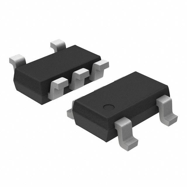
ICGOO电子元器件商城为您提供CAT4237TD-GT3由ON Semiconductor设计生产,在icgoo商城现货销售,并且可以通过原厂、代理商等渠道进行代购。 CAT4237TD-GT3价格参考。ON SemiconductorCAT4237TD-GT3封装/规格:PMIC - LED 驱动器, LED Driver IC 1 Output DC DC Regulator Step-Up (Boost) Analog, PWM Dimming 40mA TSOT-23-5。您可以下载CAT4237TD-GT3参考资料、Datasheet数据手册功能说明书,资料中有CAT4237TD-GT3 详细功能的应用电路图电压和使用方法及教程。
ON Semiconductor(安森美)的CAT4237TD-GT3是一款专用于驱动LED的PMIC(电源管理集成电路),属于LED驱动器类别。该芯片采用恒流降压型拓扑结构,适用于需要高效、稳定LED供电的场景。

主要应用场景包括:便携式照明设备,如LED手电筒、头灯和应急灯,因其高效率和小封装适合电池供电系统;消费类电子产品中的背光驱动,例如小型LCD显示屏、键盘背光等;工业与家用照明中的低功率LED灯具,尤其适用于空间受限、要求高能效的设计;还可用于汽车内部照明,如仪表盘背光、氛围灯等,具备良好的调光性能和稳定性。

CAT4237TD-GT3支持PWM调光功能,可实现精确亮度控制,同时具有过温保护和短路保护等安全特性,提升了系统可靠性。其3mm × 3mm DFN小尺寸封装有利于节省PCB空间,适合高密度布局设计。整体上,该器件在追求小型化、高效率和长电池寿命的应用中表现优异。
| 参数 | 数值 |
| 产品目录 | 集成电路 (IC)光电子产品 |
| 描述 | IC LED DRVR WHT BCKLGHT TSOT23-5LED照明驱动器 LED Driver,Boost 8 LED,series |
| 产品分类 | |
| 品牌 | ON Semiconductor |
| 产品手册 | |
| 产品图片 |
|
| rohs | 符合RoHS无铅 / 符合限制有害物质指令(RoHS)规范要求 |
| 产品系列 | LED照明电子器件,LED照明驱动器,ON Semiconductor CAT4237TD-GT3- |
| 数据手册 | |
| 产品型号 | CAT4237TD-GT3 |
| 产品目录页面 | |
| 产品种类 | LED照明驱动器 |
| 低电平输出电流 | 1 mA |
| 供应商器件封装 | TSOT-23-5 |
| 其它名称 | CAT4237TD-GT3DKR |
| 内部驱动器 | 是 |
| 包装 | Digi-Reel® |
| 商标 | ON Semiconductor |
| 安装类型 | 表面贴装 |
| 安装风格 | SMD/SMT |
| 封装 | Reel |
| 封装/外壳 | SOT-23-5 细型,TSOT-23-5 |
| 封装/箱体 | TSOT-23-5 |
| 工作温度 | -40°C ~ 85°C |
| 工厂包装数量 | 3000 |
| 恒压 | - |
| 恒流 | 是 |
| 拓扑 | PWM,升压(升压) |
| 最大工作温度 | + 85 C |
| 最大电源电流 | 1.5 mA |
| 最小工作温度 | - 40 C |
| 标准包装 | 1 |
| 电压-电源 | 2.8 V ~ 5.5 V |
| 电压-输出 | 30V |
| 类型-初级 | 背光 |
| 类型-次级 | 白色 LED |
| 系列 | CAT4237 |
| 输入电压 | 2.8 V to 5.5 V |
| 输出数 | 1 |
| 频率 | 800kHz ~ 1.3MHz |
| 高电平输出电流 | 40 mA |


- 商务部:美国ITC正式对集成电路等产品启动337调查
- 曝三星4nm工艺存在良率问题 高通将骁龙8 Gen1或转产台积电
- 太阳诱电将投资9.5亿元在常州建新厂生产MLCC 预计2023年完工
- 英特尔发布欧洲新工厂建设计划 深化IDM 2.0 战略
- 台积电先进制程称霸业界 有大客户加持明年业绩稳了
- 达到5530亿美元!SIA预计今年全球半导体销售额将创下新高
- 英特尔拟将自动驾驶子公司Mobileye上市 估值或超500亿美元
- 三星加码芯片和SET,合并消费电子和移动部门,撤换高东真等 CEO
- 三星电子宣布重大人事变动 还合并消费电子和移动部门
- 海关总署:前11个月进口集成电路产品价值2.52万亿元 增长14.8%


PDF Datasheet 数据手册内容提取
CAT4237 High Voltage CMOS Boost White LED Driver Description The CAT4237 is a DC/DC step−up converter that delivers an accurate constant current ideal for driving LEDs. Operation at a http://onsemi.com constant switching frequency of 1 MHz allows the device to be used with small value external ceramic capacitors and inductor. LEDs connected in series are driven with a regulated current set by the 5 external resistor R . LED currents up to 40 mA can be supported over 1 1 a wide range of input supply voltages from 2.8 V to 5.5 V, making the TSOT−23 device ideal for battery−powered applications. The CAT4237 TD SUFFIX high−voltage output stage is perfect for driving six, seven or eight CASE 419AE white LEDs in series with inherent current matching in LCD backlight applications. PIN CONNECTIONS LED dimming can be done by using a DC voltage, a logic signal, or 1 a pulse width modulation (PWM) signal. The shutdown input pin SW VIN allows the device to be placed in power−down mode with “zero” quiescent current. GND In addition to thermal protection and overload current limiting, the FB SHDN device also enters a very low power operating mode during “Open LED” fault conditions. The device is housed in a low profile (1mm (Top View) max height) 5−lead thin SOT23 package for space critical applications. MARKING DIAGRAMS Features • Drives 6 to 8 White LEDs in Series from 3 V LTYM UDYM • Up to 87% Efficiency • Low Quiescent Ground Current 0.6 mA • Adjustable Output Current (up to 40 mA) LT = CAT4237TD−T3 • High Frequency 1 MHz Operation UD = CAT4237TD−GT3 • Y = Production Year (Last Digit) High Voltage Power Switch M = Production Month (1−9, A, B, C) • Shutdown Current Less than 1 (cid:2)A • Open LED Low Power Mode ORDERING INFORMATION (Note 3) • Automatic Shutdown at 1.9 V (UVLO) • Device Package Shipping (Note 4) Thermal Shutdown Protection • CAT4237TD−T3 TSOT−23 3,000/ Thin SOT23 5−lead (1 mm Max Height) (Note 1) (Pb−Free) Tape & Reel • These Devices are Pb−Free, Halogen Free/BFR Free and are RoHS CAT4237TD−GT3 TSOT−23 3,000/ Compliant (Note 2) (Pb−Free) Tape & Reel Applications 1. Matte−Tin Plated Finish (RoHS−compliant). • 2. NiPdAu Plated Finish (RoHS−compliant) Color LCD and Keypad Backlighting • 3. For detailed information and a breakdown of Cellular Phones device nomenclature and numbering systems, • Handheld Devices please see the ON Semiconductor Device No- • menclature document, TND310/D, available at Digital Cameras www.onsemi.com • PDAs 4. For information on tape and reel specifications, in- • Portable Game Machine cluding part orientation and tape sizes, please refer to our Tape and Reel Packaging Specifica- tions Brochure, BRD8011/D. © Semiconductor Components Industries, LLC, 2011 1 Publication Order Number: November, 2011 − Rev. 3 CAT4237/D
CAT4237 VIN L D VOUT 3 V to 33 (cid:2)H 4.2 V C1 C2 4.7 (cid:2)F SW 0.22 (cid:2)F VIN CAT4237 OFF ON SHDN FB VFB = 300 mV 20 mA GND R1 15 (cid:3) L: Sumida CDRH3D16−330 D: Central CMDSH05−4 (rated 40 V) C2: Taiyo Yuden UMK212BJ224 (rated 50 V) Figure 1. Typical Application Circuit Table 1. ABSOLUTE MAXIMUM RATINGS Parameters Ratings Units VIN, FB voltage −0.3 to +7 V SHDN voltage −0.3 to +7 V SW voltage −0.3 to +55 V Storage Temperature Range −65 to +160 (cid:2)C Junction Temperature Range −40 to +150 (cid:2)C Lead Temperature 300 (cid:2)C Stresses exceeding Maximum Ratings may damage the device. Maximum Ratings are stress ratings only. Functional operation above the Recommended Operating Conditions is not implied. Extended exposure to stresses above the Recommended Operating Conditions may affect device reliability. Table 2. RECOMMENDED OPERATING CONDITIONS Parameters Range Units VIN 2.8 to 5.5 V SW pin voltage 0 to 30 V Ambient Temperature Range −40 to +85 (cid:2)C 6, 7 or 8 LEDs 1 to 40 mA NOTE: Typical application circuit with external components is shown above. 5. Thin SOT23−5 package thermal resistance (cid:4)JA = 135°C/W when mounted on board over a ground plane. http://onsemi.com 2
CAT4237 Table 3. DC ELECTRICAL CHARACTERISTICS (VIN = 3.6 V, ambient temperature of 25°C (over recommended operating conditions unless otherwise specified)) Symbol Parameter Conditions Min Typ Max Unit IQ Operating Current VFB = 0.2 V 0.6 1.5 mA VFB = 0.4 V (not switching) 0.1 0.6 ISD Shutdown Current VSHDN = 0 V 0.1 1 (cid:2)A VFB FB Pin Voltage 8 LEDs with ILED = 20 mA 285 300 315 mV IFB FB pin input leakage 1 (cid:2)A ILED Programmed LED Current R1 = 10 (cid:3) 28.5 30 31.5 mA R1 = 15 (cid:3) 19 20 21 R1 = 20 (cid:3) 14.25 15 15.75 VIH SHDN Logic High Enable Threshold Level 0.8 1.5 V VIL SHDN Logic Low Shutdown Threshold Level 0.4 0.7 FSW Switching Frequency 0.8 1.0 1.3 MHz ILIM Switch Current Limit 350 450 600 mA RSW Switch “On” Resistance ISW = 100 mA 1.0 2.0 (cid:3) ILEAK Switch Leakage Current Switch Off, VSW = 5 V 1 5 (cid:2)A Thermal Shutdown 150 °C Thermal Hysteresis 20 °C VUVLO Undervoltage Lockout (UVLO) Threshold 1.9 V VOV-SW Overvoltage Threshold 35 V Pin Description VIN is the supply input for the internal logic. The device is SW pin is connected to the drain of the internal CMOS compatible with supply voltages down to 2.8 V and up to power switch of the boost converter. The inductor and the 5.5V. It is recommended that a small bypass ceramic Schottky diode anode should be connected to the SW pin. capacitor (4.7 (cid:2)F) be placed between the VIN and GND pins Traces going to the SW pin should be as short as possible near the device. If the supply voltage drops below 1.9 V, the with minimum loop area. An over-voltage detection circuit device stops switching. is connected to the SW pin. When the voltage reaches 35V, the device enters a low power operating mode preventing the SHDN is the shutdown logic input. When the pin is tied to SW voltage from exceeding the maximum rating. a voltage lower than 0.4 V, the device is in shutdown mode, drawing nearly zero current. When the pin is connected to a FB feedback pin is regulated at 0.3 V. A resistor connected voltage higher than 1.5 V, the device is enabled. between the FB pin and ground sets the LED current according to the formula: GND is the ground reference pin. This pin should be connected directly to the ground place on the PCB. 0.3V I (cid:2) LED R 1 The lower LED cathode is connected to the FB pin. Table 4. PIN DESCRIPTIONS Pin # Name Function 1 SW Switch pin. This is the drain of the internal power switch. 2 GND Ground pin. Connect the pin to the ground plane. 3 FB Feedback pin. Connect to the last LED cathode. 4 SHDN Shutdown pin (Logic Low). Set high to enable the driver. 5 VIN Power Supply input. http://onsemi.com 3
CAT4237 Block Diagram VIN 33 (cid:2)H SW C1 C2 4.7 (cid:2)F 0.22 (cid:2)F 1 MHz Over Voltage Oscillator Protection 300 mV VIN VREF – A1 + Driver LED PWM & Current + A2 Logic Enable RC – N1 CC Thermal SHDN Shutdown + RS & UVLO GND – Current Sense FB R1 15 (cid:3) Figure 2. Block Diagram Device Operation Thermal overload protection circuitry has been included The CAT4237 is a fixed frequency (1 MHz), low noise, to prevent the device from operating at unsafe junction inductive boost converter that provides a constant current temperatures above 150°C. In the event of a thermal with excellent line and load regulation. The device uses a overload condition the device will automatically shutdown high-voltage CMOS power switch between the SW pin and and wait till the junction temperatures cools to 130°C before ground to energize the inductor. When the switch is turned normal operation is resumed. off, the stored energy in the inductor is released into the load via the Schottky diode. Light Load Operation Under light load condition (under 4 mA) and with input The on/off duty cycle of the power switch is internally voltage above 4.2 V, the CAT4237 driving 6 LEDs, the adjusted and controlled to maintain a constant regulated driver starts pulse skipping. Although the LED current voltage of 0.3 V across the feedback resistor connected to the remains well regulated, some lower frequency ripple may feedback pin (FB). The value of the resistor sets the LED appear. current accordingly (0.3 V/R ). 1 During the initial power-up stage, the duty cycle of the internal power switch is limited to prevent excessive in-rush currents and thereby provide a “soft-start” mode of operation. While in normal operation, the device can deliver up to 40mA of load current into a string of up to 8 white LEDs. In the event of an “Open LED” fault condition, where the feedback control loop becomes open, the output voltage will continue to increase. Once this voltage exceeds 35 V, an internal protection circuit will become active and place the device into a very low power safe operating mode where only a small amount of power is transferred to the output. This is achieved by pulsing the switch once every 60 (cid:2)s and keep it on for about 1 (cid:2)s only. Figure 3. Switching Waveform V = 4.2 V, IN I = 4 mA LED http://onsemi.com 4
CAT4237 TYPICAL CHARACTERISTICS (VIN = 3.6 V, CIN = 4.7 (cid:2)F, COUT = 0.22 (cid:2)F, L = 33 (cid:2)H with 8 LEDs at 20 mA, TAMB = 25°C, unless otherwise specified.) 140 2.0 120 A) mA) 1.5 (cid:2)NT ( 100 NT ( E 80 E R R R R 1.0 U U C 60 C UT VFB = 0.4 V PLY NP 40 (not switching) UP 0.5 I S 20 0 0 2.7 3.0 3.3 3.6 3.9 4.2 4.5 4.8 2.5 3.0 3.5 4.0 4.5 5.0 INPUT VOLTAGE (V) INPUT VOLTAGE (V) Figure 4. Quiescent Current vs. V Figure 5. Quiescent Current vs. V IN IN (Not Switching) (Switching) 315 315 8 LEDs at 20 mA 310 310 VOUT = 26 V V) 8 LEDs mV) 305 E (m 305 K ( AG AC 300 LT 300 B O D V E N FE 295 PI 295 B F 290 290 285 285 2.7 3.0 3.3 3.6 3.9 4.2 4.5 4.8 0 5 10 15 20 25 30 INPUT VOLTAGE (V) OUTPUT CURRENT (mA) Figure 6. FB Pin Voltage vs. Supply Voltage Figure 7. FB Pin Voltage vs. Output Current 1040 SW pin 20V/div z)1020 H k Y ( C Inductor N1000 Current E 100mA/div U Q E R F 980 VOUT AC coupled 200mV/div 960 2.7 3.0 3.3 3.6 3.9 4.2 4.5 4.8 0.5 (cid:2)sec/div INPUT VOLTAGE (V) Figure 8. Switching Frequency vs. Supply Figure 9. Switching Waveforms Voltage http://onsemi.com 5
CAT4237 TYPICAL CHARACTERISTICS (VIN = 3.6 V, CIN = 4.7 (cid:2)F, COUT = 0.22 (cid:2)F, L = 33 (cid:2)H with 8 LEDs at 20 mA, TAMB = 25°C, unless otherwise specified.) 35 1.0 30 RFB = 10 (cid:3) %) A) 25 N ( 0.5 m O ENT ( 20 RFB = 15 (cid:3) RIATI RR RFB = 20 (cid:3) VA 0 U 15 T C N D E E 10 R L R −0.5 U C 5 0 −1.0 2.5 3.0 3.5 4.0 4.5 5.0 3.0 3.3 3.6 3.9 4.2 4.5 4.8 INPUT VOLTAGE (V) INPUT VOLTAGE (V) Figure 10. LED Current vs. Input Voltage Figure 11. LED Current Regulation (20 mA) (8 LEDs) 90 90 VIN = 4.2 V 20 mA 85 85 %) %) 15 mA Y ( 80 VIN = 3.6 V Y ( 80 C C N N E E CI CI FI 75 FI 75 F F E E 8 LEDs 8 LEDs 70 VOUT ~ 27 V at 20 mA 70 VOUT ~ 27 V at 20 mA L = 33 (cid:2)H L = 33 (cid:2)H 65 65 5 10 15 20 25 30 3.0 3.5 4.0 4.5 5.0 LED CURRENT (mA) INPUT VOLTAGE (V) Figure 12. 8 LED Efficiency vs. Load Current Figure 13. 8 LED Efficiency vs. Input Voltage 90 90 VIN = 4.2 V VIN = 4.2 V 85 85 VIN = 3.6 V VIN = 3.6 V %) %) Y ( 80 Y ( 80 C C N N E E CI CI FI 75 FI 75 F F E E 7 LEDs 6 LEDs 70 VOUT ~ 23 V at 20 mA 70 VOUT ~ 20 V at 20 mA L = 33 (cid:2)H L = 33 (cid:2)H 65 65 5 10 15 20 25 30 5 10 15 20 25 30 LED CURRENT (mA) LED CURRENT (mA) Figure 14. 7 LED Efficiency vs. Load Current Figure 15. 6 LED Efficiency vs. Load Current http://onsemi.com 6
CAT4237 TYPICAL CHARACTERISTICS (VIN = 3.6 V, CIN = 4.7 (cid:2)F, COUT = 0.22 (cid:2)F, L = 33 (cid:2)H with 8 LEDs at 20 mA, TAMB = 25°C, unless otherwise specified.) 2.0 EN 5V/div (cid:3)) VOUT E ( 1.5 C 10V/div N A T S SI 1.0 E R Input H C Current T 100mA/ WI 0.5 div S 0 2.5 3.0 3.5 4.0 4.5 50 (cid:2)sec/div INPUT VOLTAGE (V) Figure 16. Power−up with 8 LEDs at 20 mA Figure 17. Switch ON Resistance vs. Input Voltage 303 1.0 GE (mV) 330012 AGE (V) 0.8 −2450°°CC A T LT OL 85°C O 300 V 0.6 K V WN 125°C C O BA 299 D D T E U 0.4 FE 298 VIN = 3.6 V, 8 LEDs SH ILED = 20 mA 297 0.2 −50 0 50 100 150 3.0 3.5 4.0 4.5 5.0 TEMPERATURE (°C) INPUT VOLTAGE (V) Figure 18. FB Pin Voltage vs. Temperature Figure 19. Shutdown Voltage vs. Input Voltage 140 A) 120 m T ( N 100 E VOUT = 15 V R R 80 U C T U 60 P VOUT = 20 V T U 40 O X A M 20 0 2.5 3.0 3.5 4.0 4.5 5.0 INPUT VOLTAGE (V) Figure 20. Maximum Output Current vs. Input Voltage http://onsemi.com 7
CAT4237 Application Information given current. In order to achieve the best efficiency, this forward voltage should be as low as possible. The response External Component Selection time is also critical since the driver is operating at 1MHz. Central Semiconductor Schottky diode CMDSH05−4 Capacitors (500mA rated) is recommended for most applications. The CAT4237 only requires small ceramic capacitors of 4.7(cid:2)F on the input and 0.22 (cid:2)F on the output. Under normal LED Current Setting condition, a 4.7 (cid:2)F input capacitor is sufficient. For The LED current is set by the external resistor R 1 applications with higher output power, a larger input connected between the feedback pin (FB) and ground. The capacitor of 10 (cid:2)F may be appropriate. X5R and X7R formula below gives the relationship between the resistor capacitor types are ideal due to their stability across and the current: temperature range. 0.3V R (cid:2) current Inductor 1 LED A 33 (cid:2)H inductor is recommended for most of the CAT4237 applications. In cases where the efficiency is Table 5. RESISTOR R1 AND LED CURRENT critical, inductances with lower series resistance are LED Current (mA) R1 ((cid:2)) preferred. Inductors with current rating of 300 mA or higher 5 60 are recommended for most applications. Sumida CDRH3D16−330 33 (cid:2)H inductor has a rated current of 10 30 320mA and a series resistance (D.C.R.) of 520 m(cid:3) typical. 15 20 20 15 Schottky Diode The current rating of the Schottky diode must exceed the 25 12 peak current flowing through it. The Schottky diode 30 10 performance is rated in terms of its forward voltage at a http://onsemi.com 8
CAT4237 Open LED Protection In the event of an “Open LED” fault condition, the 2.0 CAT4237 will continue to boost the output voltage with maximum power until the output voltage reaches A) approximately 35 V. Once the output exceeds this level, the m 1.5 internal circuitry immediately places the device into a very T ( N low power mode where the total input power is limited to E R about 4 mW (about 1 mA input current with a 3.6 V supply). R 1.0 U The SW pin clamps at a voltage below its maximum rating C Y of 60 V. There is no need to use an external zener diode PL P between Vout and the FB pin. A 50 V rated C2 capacitor is U 0.5 S required to prevent any overvoltage damage in the open LED condition. 0 Schottky 100 V 2.5 3.0 3.5 4.0 4.5 5.0 (Central CMSH1−100) L INPUT VOLTAGE (V) VIN 33 (cid:2)H VOUT Figure 23. Open LED Supply Current vs. VIN without C1 C2 Zener 4.7 (cid:2)F 0.22 (cid:2)F 50 SW VIN CAT4237 OFF ON SHDN FB VFB = 300 mV E (V) 45 G GND R1 A 15 (cid:3) LT O 40 V T Figure 21. Open LED Protection without Zener U P T U O 35 30 2.5 3.0 3.5 4.0 4.5 5.0 INPUT VOLTAGE (V) Figure 24. Open LED Output Voltage vs. V without IN Zener SW PIN 10 V/div 10 (cid:2)sec/div Figure 22. Open LED Switching Waveforms without Zener http://onsemi.com 9
CAT4237 Dimming Control There are several methods available to control the LED brightness. VIN SW CAT4237 PWM Signal on the SHDN Pin SHDN LED brightness dimming can be done by applying a PWM GND FB signal to the SHDN input. The LED current is repetitively PWN turned on and off, so that the average current is proportional Signal VFB = 300 mV LED 2.5 V 3.73 k(cid:3) 3.1 k(cid:3) 1 k(cid:3) Current to the duty cycle. A 100% duty cycle, with SHDN always high, corresponds to the LEDs at nominal current. Figure25 0 V RA C1 RB i R2 R1 shows a 1kHz signal with a 50% duty cycle applied to the 15 (cid:3) SHDN pin. The recommended PWM frequency range is 0.22 (cid:2)F from 100Hz to 2kHz. Figure 26. Circuit for Filtered PWM Signal A PWM signal at 0 V DC, or a 0% duty cycle, results in a max LED current of about 22 mA. A PWM signal with a 93% duty cycle or more, results in an LED current of 0mA. 25 20 A) m NT ( 15 E R R U C 10 D E L 5 Figure 25. Switching Waveform with 1 kHz PWM on SHDN 0 0 10 20 30 40 50 60 70 80 90 100 Filtered PWM Signal PWM DUTY CYCLE (%) A filtered PWM signal used as a variable DC voltage can Figure 27. Filtered PWM Dimming (0 V to 2.5 V) control the LED current. Figure 26 shows the PWM control circuitry connected to the CAT4237 FB pin. The PWM signal has a voltage swing of 0 V to 2.5 V. The LED current can be dimmed within a range from 0 mA to 20 mA. The PWM signal frequency can vary from very low frequency up to 100 kHz. http://onsemi.com 10
CAT4237 Board Layout The CAT4237 is a high−frequency switching regulator. when the CAT4237 switch is open. Both loop areas should The traces that carry the high−frequency switching current be as small as possible. have to be carefully layout on the board in order to minimize Capacitor C has to be placed as close as possible to the 1 EMI, ripple and noise in general. The thicker lines on V pin and GND. The capacitor C has to be connected IN 2 Figure28 show the switching current path. All these traces separately to the top LED anode. A ground plane under the have to be short and wide enough to minimize the parasitic CAT4237 allows for direct connection of the capacitors to inductance and resistance. The loop shown on Figure28 ground. The resistor R must be connected directly to the 1 corresponds to the current path when the CAT4237 internal GND pin of the CAT4237 and not shared with the switching switch is closed. On Figure 29 is shown the current loop, current loops and any other components. Open Closed Figure 28. Closed−switch Current Loop Figure 29. Open−switch Current Loop http://onsemi.com 11
CAT4237 PACKAGE DIMENSIONS TSOT−23, 5 LEAD CASE 419AE−01 ISSUE O SYMBOL MIN NOM MAX D A 1.00 e A1 0.01 0.05 0.10 A2 0.80 0.87 0.90 b 0.30 0.45 c 0.12 0.15 0.20 D 2.90 BSC E1 E E 2.80 BSC E1 1.60 BSC e 0.95 TYP L 0.30 0.40 0.50 L1 0.60 REF L2 0.25 BSC θ 0º 8º TOP VIEW A2 A (cid:4) L b A1 c L2 L1 SIDE VIEW END VIEW Notes: (1) All dimensions are in millimeters. Angles in degrees. (2) Complies with JEDEC MO-193. ON Semiconductor and are registered trademarks of Semiconductor Components Industries, LLC (SCILLC). SCILLC reserves the right to make changes without further notice to any products herein. SCILLC makes no warranty, representation or guarantee regarding the suitability of its products for any particular purpose, nor does SCILLC assume any liability arising out of the application or use of any product or circuit, and specifically disclaims any and all liability, including without limitation special, consequential or incidental damages. “Typical” parameters which may be provided in SCILLC data sheets and/or specifications can and do vary in different applications and actual performance may vary over time. All operating parameters, including “Typicals” must be validated for each customer application by customer’s technical experts. SCILLC does not convey any license under its patent rights nor the rights of others. SCILLC products are not designed, intended, or authorized for use as components in systems intended for surgical implant into the body, or other applications intended to support or sustain life, or for any other application in which the failure of the SCILLC product could create a situation where personal injury or death may occur. Should Buyer purchase or use SCILLC products for any such unintended or unauthorized application, Buyer shall indemnify and hold SCILLC and its officers, employees, subsidiaries, affiliates, and distributors harmless against all claims, costs, damages, and expenses, and reasonable attorney fees arising out of, directly or indirectly, any claim of personal injury or death associated with such unintended or unauthorized use, even if such claim alleges that SCILLC was negligent regarding the design or manufacture of the part. SCILLC is an Equal Opportunity/Affirmative Action Employer. This literature is subject to all applicable copyright laws and is not for resale in any manner. PUBLICATION ORDERING INFORMATION LITERATURE FULFILLMENT: N. American Technical Support: 800−282−9855 Toll Free ON Semiconductor Website: www.onsemi.com Literature Distribution Center for ON Semiconductor USA/Canada P.O. Box 5163, Denver, Colorado 80217 USA Europe, Middle East and Africa Technical Support: Order Literature: http://www.onsemi.com/orderlit Phone: 303−675−2175 or 800−344−3860 Toll Free USA/Canada Phone: 421 33 790 2910 Fax: 303−675−2176 or 800−344−3867 Toll Free USA/Canada Japan Customer Focus Center For additional information, please contact your local Email: orderlit@onsemi.com Phone: 81−3−5817−1050 Sales Representative http://onsemi.com CAT4237/D 12
Mouser Electronics Authorized Distributor Click to View Pricing, Inventory, Delivery & Lifecycle Information: O N Semiconductor: CAT4237TD-GT3