ICGOO在线商城 > 集成电路(IC) > PMIC - LED 驱动器 > CAT3224HV3-GT2
 Datasheet下载
- 型号: CAT3224HV3-GT2
- 制造商: ON Semiconductor
- 库位|库存: xxxx|xxxx
- 要求:
| 数量阶梯 | 香港交货 | 国内含税 |
| +xxxx | $xxxx | ¥xxxx |
查看当月历史价格
查看今年历史价格
CAT3224HV3-GT2产品简介:
ICGOO电子元器件商城为您提供CAT3224HV3-GT2由ON Semiconductor设计生产,在icgoo商城现货销售,并且可以通过原厂、代理商等渠道进行代购。 CAT3224HV3-GT2价格参考。ON SemiconductorCAT3224HV3-GT2封装/规格:PMIC - LED 驱动器, LED 驱动器 IC 2 输出 DC DC 稳压器 开关电容器(充电泵) 2A(闪存) 16-TQFN(3x3)。您可以下载CAT3224HV3-GT2参考资料、Datasheet数据手册功能说明书,资料中有CAT3224HV3-GT2 详细功能的应用电路图电压和使用方法及教程。
CAT3224HV3-GT2 是一款由 ON Semiconductor 提供的 PMIC - LED 驱动器,适用于多种需要高效、灵活驱动LED的应用场景。以下是其主要应用场景:

1. 便携式设备背光:CAT3224HV3-GT2 可用于驱动小型显示屏(如手机、平板电脑或可穿戴设备)的背光。它支持双通道恒流驱动,能够为多个串联或并联的白光LED提供稳定电流,确保亮度一致。

2. 汽车电子应用:该芯片适用于车内仪表盘、中控屏以及氛围灯的LED驱动。其高耐压能力(最高可达36V)和低EMI特性使其在汽车环境中表现优异,同时支持PWM调光以实现亮度调节。

3. 消费类电子产品:例如数码相机、GPS导航仪等设备中的显示屏背光。CAT3224HV3-GT2 的小尺寸封装(QFN-10)和高效能设计非常适合对空间和功耗敏感的产品。

4. 工业控制与人机界面 (HMI):在工业领域,这款芯片可以用来驱动按钮指示灯、触摸屏或液晶面板的背光源,满足长时间稳定运行的需求。

5. 智能家居设备:如智能音箱、安防摄像头的指示灯或屏幕背光。其内置保护功能(过温、短路保护等)提高了系统可靠性。

6. 医疗设备显示:在便携式健康监测仪器(如血压计、血糖仪)或其他医疗显示设备中,CAT3224HV3-GT2 能够提供精确且稳定的LED驱动能力。

总之,CAT3224HV3-GT2 凭借其高效的转换效率、灵活的配置选项以及强大的保护机制,在需要高性能LED驱动的各种应用中表现出色。
| 参数 | 数值 |
| 产品目录 | 集成电路 (IC)光电子产品 |
| 描述 | IC LED DRIVER PHOTO FLASH 16TQFNLED照明驱动器 LED Driver Charge pump 2 ch |
| 产品分类 | |
| 品牌 | ON Semiconductor |
| 产品手册 | |
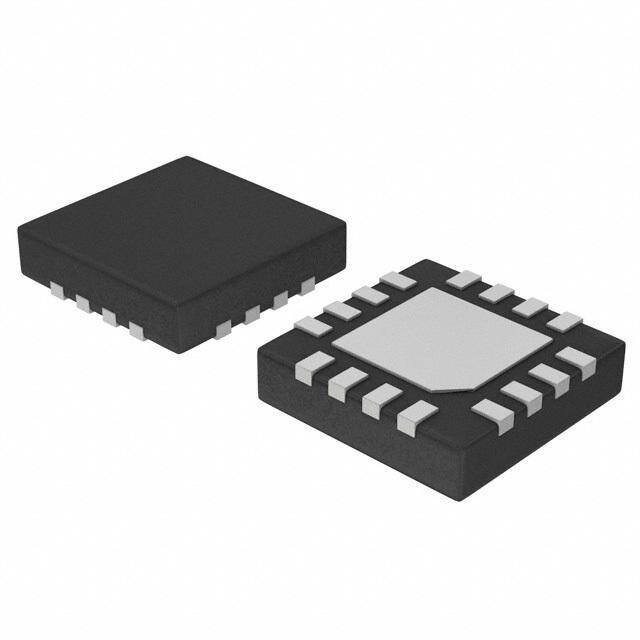
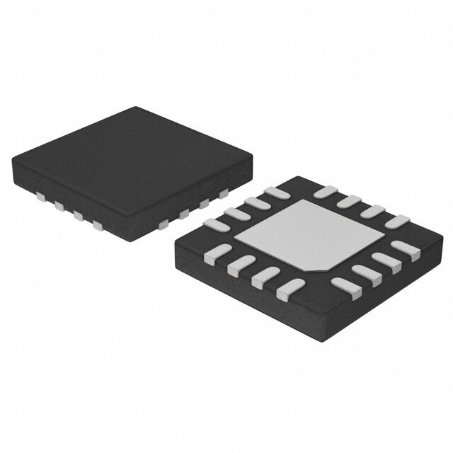
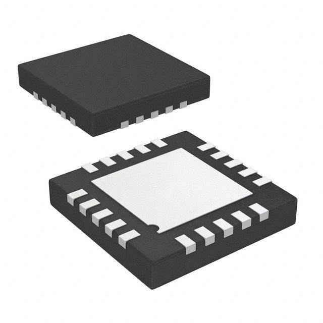
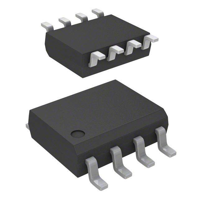
| 产品图片 |
|
| rohs | 符合RoHS无铅 / 符合限制有害物质指令(RoHS)规范要求 |
| 产品系列 | LED照明电子器件,LED照明驱动器,ON Semiconductor CAT3224HV3-GT2- |
| 数据手册 | |
| 产品型号 | CAT3224HV3-GT2 |
| 产品目录页面 | |
| 产品种类 | LED照明驱动器 |
| 供应商器件封装 | 16-TQFN(3x3) |
| 其它名称 | CAT3224HV3-GT2CT |
| 内部驱动器 | 是 |
| 包装 | 剪切带 (CT) |
| 商标 | ON Semiconductor |
| 安装类型 | 表面贴装 |
| 安装风格 | SMD/SMT |
| 封装 | Reel |
| 封装/外壳 | 16-WFQFN 裸露焊盘 |
| 封装/箱体 | TQFN-16 |
| 工作温度 | -40°C ~ 85°C |
| 工厂包装数量 | 2000 |
| 恒压 | - |
| 恒流 | - |
| 拓扑 | 切换式电容器(充电泵) |
| 最大工作温度 | + 85 C |
| 最大电源电流 | 2 A |
| 最小工作温度 | - 40 C |
| 标准包装 | 1 |
| 电压-电源 | 2 V ~ 5.5 V |
| 电压-输出 | - |
| 类型-初级 | 闪灯/白光 |
| 类型-次级 | - |
| 系列 | CAT3224 |
| 输入电压 | 2.5 V to 5.5 V |
| 输出数 | 2 |
| 频率 | 800kHz |


- 商务部:美国ITC正式对集成电路等产品启动337调查
- 曝三星4nm工艺存在良率问题 高通将骁龙8 Gen1或转产台积电
- 太阳诱电将投资9.5亿元在常州建新厂生产MLCC 预计2023年完工
- 英特尔发布欧洲新工厂建设计划 深化IDM 2.0 战略
- 台积电先进制程称霸业界 有大客户加持明年业绩稳了
- 达到5530亿美元!SIA预计今年全球半导体销售额将创下新高
- 英特尔拟将自动驾驶子公司Mobileye上市 估值或超500亿美元
- 三星加码芯片和SET,合并消费电子和移动部门,撤换高东真等 CEO
- 三星电子宣布重大人事变动 还合并消费电子和移动部门
- 海关总署:前11个月进口集成电路产品价值2.52万亿元 增长14.8%


PDF Datasheet 数据手册内容提取
CAT3224 4 Amp Supercapacitor Flash LED Driver Description The CAT3224 is a very high−current integrated flash LED driver which also supports the charging function for a dual−cell http://onsemi.com supercapacitor applications. Ideal for Li−ion battery−powered systems, it delivers up to 4 A LED flash pulses, far beyond the peak current capability of the battery. Dual−mode 1x/2x charge pump charges the stacked supercapacitor to a nominal voltage of 5.4 V, while an active balance control circuit TQFN−16 ensures that both capacitor cell voltages remain matched. The nominal HV3 SUFFIX charging current to be drawn from the battery is set by an external CASE 510AD resistor tied to the RC pin. The driver also features two matched current sources. External resistors provide the adjustment for the maximum flash mode current PIN CONNECTIONS (up to 4 A) and the torch mode current (up to 400 mA). A built−in D N N P N safety timer automatically terminates the flash pulse beyond a G C C VI maximum duration of 300 ms. 1 In addition to thermal shutdown and overvoltage protection, the RF RT device is fully protected against external resistor programming faults BAL RC and fully supports reverse output voltage for all conditions. CAP LEDA The device is packaged in the tiny 16−pad TQFN 3 mm x 3mm package with a max height of 0.8 mm. CAP LEDB Features G H H G • R S C A 2 Channels at 2 A Each in Flash Mode H A R L • 2 Channels at 200 mA Each in Torch Mode C FL TO F • Adjustable Charge Current Limit up to 1000 mA (Top View) • Flash/Torch Current Separate Adjustment • Dual−mode 1x/2x Charge Pump MARKING DIAGRAM • Dual Cell Supercapacitor Balancing • Flash Safety Timer and Ready Flag JAAT • Supercapacitor Continuous Charging • Shutdown CAP Leakage 3 (cid:2)A • JAAT = Specific Device Code “Zero” Current Shutdown Mode • 80 (cid:2)A Standby Current (I ) VIN • Over−voltage, Over−current Limiting ORDERING INFORMATION • Thermal Shutdown Protection Device Package Shipping • Small 3 mm x 3 mm, 16−pad TQFN Package CAT3224HV3−GT2 TQFN−16 2,000/ • This Device is Pb−Free, Halogen Free/BFR Free and RoHS (Pb−Free) Tape & Reel Compliant Note: NiPdAu Plated Finish (RoHS−compliant) Applications • High Power LED Flash • Systems with High Peak Loads © Semiconductor Components Industries, LLC, 2009 1 Publication Order Number: December, 2009 − Rev. 0 CAT3224/D
CAT3224 1 (cid:2)F Dual−Cell VIN (2.5 V to 5.5 V) CP CN Supercapacitor VIN CAP 1 (cid:2)F 1 (cid:2)F CAT3224 CAP + FLAG BAL 0.55 F CHRG LEDA – FLASH LEDB TORCH RC RF RT GND 2A 2A 826 (cid:3) 261 (cid:3) 562 (cid:3) GND Figure 1. Typical Application Circuit Table 1. ABSOLUTE MAXIMUM RATINGS Parameter Rating Unit VIN, RC, RF, RT voltage GND−0.3 to 6 V CAP, CP, CN voltage GND−0.3 to 7 V CHRG, FLASH, TORCH, FLAG voltage (Note 1) GND−0.3 to 6 V BAL, LEDA, LEDB GND−0.3 to CAP+0.3 V Storage Temperature Range −65 to +160 (cid:2)C Junction Temperature Range −40 to +150 (cid:2)C Lead Temperature 300 (cid:2)C ESD Rating HBM (Human Body Model) 2000 V ESD Rating MM (Machine Model) 200 V Stresses exceeding Maximum Ratings may damage the device. Maximum Ratings are stress ratings only. Functional operation above the Recommended Operating Conditions is not implied. Extended exposure to stresses above the Recommended Operating Conditions may affect device reliability. Table 2. RECOMMENDED OPERATING CONDITIONS Parameter Rating Unit VIN 2.0 to 5.5 V Ambient Temperature Range −40 to +85 (cid:2)C LEDA, LEDB current (in flash mode) up to 2 A LEDA, LEDB current (in torch mode) 10 to 200 mA Input Current Limit up to 1 A FLAG pull−up resistor current 0 to 10 mA LED Forward Voltage Range (Vf) 1.3 to 4.2 V Table 3. PACKAGE THERMAL IMPEDANCE Parameter Range Unit TQFN 3 mm x 3 mm 16−Lead (cid:4)JA (Note 2) 42 (cid:2)C/W Table 4. PACKAGE TRANSIENT THERMAL IMPEDANCE Parameter Range Unit TQFN 3 mm x 3 mm 16−Lead Transient (cid:4)JA (Note 3) (100 ms pulse) 7 (cid:2)C/W 1. Pins can be driven above VIN with no leakage current or change in operation. 2. (cid:4)JA (Junction to Ambient thermal resistance) is calculated with 2 square inches of copper connected to package exposed pad. 3. Transient (cid:4)JA is calculated for a 100 ms pulse at 5 watts with 2 square inches of copper connected to package exposed pad. http://onsemi.com 2
CAT3224 Table 5. ELECTRICAL OPERATING CHARACTERISTICS (VIN = 3.6 V, EN = 1.3 V, TAMB = 25°C unless otherwise stated.) Symbol Name Conditions Min Typ Max Units IQVIN Quiescent Current on VIN pin (IIN – 2 x IOUT) CAP Charged & idle 80 (cid:2)A CAP Charging 2x Mode 6 mA IQCAP Quiescent Current on CAP pin CAP Charged & idle 10 (cid:2)A Shutdown mode 3 (cid:2)A Shutdown, VIN = 0 V 3 (cid:2)A IQSHDN Shutdown Current CHRG = FLASH = TORCH = 0 V 1 (cid:2)A GFLASH Flash Gain (IFLASH / IRF) IFLASH = 2 A 900 GTORCH Torch Gain (ITORCH / IRT) ITORCH = 200 mA 120 GCHARGE Input Current Limit Gain (ICHRG / IRC) ICHARGE = 400 mA 400 VRX RSET Regulated Voltage (VRF VRT VRC) IRX = 0.1 mA 0.59 0.6 0.61 V IRX_MAX Rset Current limit (IRF IRT IRC) VRX = 0 V 3.5 mA IIN_MAX Input current limit in charge mode VRC = 0 V 1.4 A VC_OFF CAP Charge off voltage RC = 2 k(cid:3) 5.4 V VC_HYST CAP Charge Hysteresis 0.2 V VF_ON CAP voltage FLAG pulled low 5.2 V VF_HYST CAP voltage FLAG Hysteresis 0.2 V RLEDAB LEDA/B Combined Dropout Resistance IFLASHAB = 4 A 110 m(cid:3) RCP Charge Mode Resistance 1x mode 2 (cid:3) 2x mode, VIN = 3.5 V 4 (cid:3) FOSC Charge Pump Frequency 800 kHz TFLASH Flash Timeout Duration 300 ms VFLAG Flag low voltage threshold (Open Drain) FLAG Driven low 100 (cid:2)A pull−up 0.2 V CHRG, FLASH, TORCH Pin REN Internal Pull−down Resistor 150 k(cid:3) VEHI Logic High Level 1.3 V VELO Logic Low Level 0.4 V VBAL Active Balance Control (VCAP / 2) ±5 mA Load on BAL −2 +2 % TSD Thermal Shutdown 150 °C THYS Thermal Hysteresis 20 °C VUVLO Undervoltage lockout (UVLO) threshold 1.9 V http://onsemi.com 3
CAT3224 Cap Voltage and Flag Output The timing diagram in Figure 2 shows the CAP output voltage and the FLAG output in charge mode (with CHRG input high). CAP VOLTAGE VC OFF VC HYST VF ON VF HYST TIME Charge Current 0 A FLAG FLASH LED Current 0 A Figure 2. Supercapacitor Charge Timing Diagram http://onsemi.com 4
CAT3224 TYPICAL CHARACTERISTICS (VIN = 3.6 V, C = 0.55 F, TAMB = 25°C, typical application circuit unless otherwise specified.) 100 1.0 90 (cid:2)A) (A)E (N 80 RG VI A Q H I C I 70 60 0.1 3.0 3.5 4.0 4.5 5.0 5.5 0.1 1.0 10 INPUT VOLTAGE (V) RC (k(cid:3)) Figure 3. Idle Quiescent Current vs. Input Figure 4. Charge Current vs. R C Voltage 10 1,000 A) mA) (FLASH 1.0 (ORCH 100 I T I 0.1 10 0.1 1.0 10 0.1 1.0 10 RF (k(cid:3)) RT (k(cid:3)) Figure 5. Flash LED Current vs. R Figure 6. Torch LED Current vs. R F T 20 15 (cid:3)) (ON 10 S D R 5 0 3.0 3.5 4.0 4.5 5.0 5.5 INPUT VOLTAGE (V) Figure 7. FLAG R vs. Input Voltage DSON http://onsemi.com 5
CAT3224 TYPICAL CHARACTERISTICS (VIN = 3.6 V, C = 0.55 F, TAMB = 25°C, typical application circuit unless otherwise specified.) 630 630 620 620 610 610 V) V) m m (F 600 (C 600 R R V V 590 590 580 580 570 570 0 0.5 1.0 1.5 2.0 0 0.2 0.4 0.6 0.8 1.0 IFLASH (A) ICHARGE (A) Figure 8. V vs. I Figure 9. V vs. I RF FLASH RC CHARGE 630 6.0 620 5.5 610 mV) (V)F (T 600 OF 5.0 VR VC_ 590 4.5 580 570 4.0 0 50 100 150 200 0 0.5 1.0 1.5 2.0 2.5 3.0 ITORCH (mA) RC (k(cid:3)) Figure 10. V vs. I Figure 11. V idle vs. R RT TORCH CAP C 500 400 A) 300 m (T U O 200 I Vled = 2.9 V 100 0 3.0 3.5 4.0 4.5 5.0 5.5 VCAP (V) Figure 12. Torch Output Current vs. V CAP http://onsemi.com 6
CAT3224 TYPICAL CHARACTERISTICS (VIN = 3.6 V, C = 0.55 F, TAMB = 25°C, typical application circuit unless otherwise specified.) CHRG CHRG 5V/div 5V/div CAP CAP 2V/div 2V/div Input Input Current Current 1A/div 500mA/div 1s/div 2s/div Figure 13. Charge Cycle, 1 A Input Current Figure 14. Charge Cycle, 500 mA Input Current CHRG FLASH 5V/div 5V/div CAP 2V/div LED Current 1A/div Input Current 500mA/ div 4s/div 40 (cid:2)s/div Figure 15. Charge Cycle, 300 mA Input Current Figure 16. FLASH Transient Response CHRG 5V/div Input Current 500mA/div CAP 2V/div FLAG 5V/div 2s/div Figure 17. Charge Cycle with FLAG http://onsemi.com 7
CAT3224 Table 6. PIN DESCRIPTION Pin # Name Function 1 RF Flash Current Setting Resistor terminal 2 BAL Active Supercapacitor Balance Control 3, 4 CAP Supercapacitor Positive Connection 5 CHRG Charge Supercapacitor Enable 6 FLASH Flash Enable 7 TORCH Torch Enable 8 FLAG Flash Ready Flag output, Open drain (Active low) 9 LEDB LED B channel anode (+) connection 10 LEDA LED A channel anode (+) connection 11 RC Charge Current Setting Resistor terminal 12 RT Torch Current Setting Resistor terminal 13 VIN Positive supply connection to battery 14 CP Bucket capacitor Positive terminal 15 CN Bucket capacitor Negative terminal 16 GND Device ground connection TAB TAB Connect to GND on the PCB Pin Function VIN is the supply pin for the device and for the RF is connected to a resistor (R ) to set the current in the F supercapacitor charger circuit. A small 1 (cid:2)F ceramic bypass LED channels in flash mode. The voltage on the pin is capacitor is required between the VIN pin and ground near regulated to 0.6 V in flash mode (FLASH high). the device. RT is connected to a resistor (R ) to set the current in the T GND is the ground reference for the charge pump. This pin LED channels in torch mode. The voltage on the pin is must be connected to the ground plane on the PCB. regulated to 0.6 V in torch mode (TORCH high). TAB is the exposed pad underneath the package. For best RC is connected to a resistor (R ) to set the current limit on C thermal performance, the tab should be soldered to the PCB VIN when charging the supercapacitor. The voltage on the and connected to the ground plane. pin is regulated to 0.6 V in charge mode (CHRG high). CAP is the positive connection to the supercapacitor. CHRG is the charge mode enable pin. When high, the 1x/2x Current sinks or sources from this pin to the capacitor charge pump is enabled and allows to charge the depending on the mode of operation. supercapacitor and monitors its voltage. CP, CN pins are connected to each side of the ceramic FLASH is the flash mode enable pin. When high, the LED bucket capacitor used in the 2x charge pump mode. current sources are enabled in flash mode. If FLASH is kept high for longer then 300 ms typical, the LED channels are LEDA, LEDB are connected internally to the current automatically disabled. sources and must be connected to the LED anodes. Each output is independently current regulated. These pins enter TORCH is the torch mode enable pin. When high, the LED a high−impedance ‘zero’ current state whenever the device current sources are enabled in torch mode. is placed in shutdown mode or FLASH and TORCH are low. FLAG is an active−low open−drain output that notify to the BAL is connected to the center−point between the two microcontroller that the supercapacitor is fully charged by supercapacitor cells. An active circuit forces the BAL pin to pulling the output low. When using the flag, this pin should remain at half of the voltage of the CAP output. be connected to a positive rail via an external pull−up resistor. http://onsemi.com 8
CAT3224 Block Diagram Figure 18. Functional Block Diagram http://onsemi.com 9
CAT3224 Basic Operation The CAT3224 integrates in a single device two main current should be less than half the charging current. If the functions: a dual cell supercapacitor charger and an LED requested torch current is greater than half the input current, driver. Two LED channels provide accurately regulated and the LEDs will dim progressively according to the input matched current up to 2 A per channel. The charging mode current. is activated when the CHRG control input is pulled high and can remain active even during torch or flash mode. This Flash Mode When the FLASH input is set high, the driver is in flash allows continuous torch mode operation. The two modes, mode and the LED channel current is set according to the torch and flash, are activated using separate control inputs external resistor connected between the RF pin and ground. repectively TORCH and FLASH. The flash mode LED channel current can be calculated by Charge Mode the following equation (approximation). When the CHRG input is set high, the driver is in charge V 0.6V mode and the input supply current cannot exceed the current I (cid:2)900(cid:3)I (cid:4)900(cid:3) RF(cid:4)900(cid:3) FLASH RF R R limit set by an external resistor connected between the RC F F Table 7 shows some standard resistor values for R and the pin and ground. The charging current limit is calculated by F corresponding LED channel current. the following equation (approximation). I (cid:2)400(cid:3)I (cid:4)400(cid:3)VRC(cid:4)400(cid:3)0.6V Table 7. RSET Resistor Settings IN RC RC RC LED Current per Channel [A] RF [(cid:2)] If the CAP output voltage is lower than the charge 1 549 threshold, the charging cycle starts. The driver charge pump 1.5 360 initially starts in 1x mode and remains there as long as the supply voltage VIN is high enough to drive the CAP output 2 261 voltage directly. In 1x mode, the output current charging the The maximum flash duration where the LED current is supercapacitor is approximately equal to the input current. regulated depends on the initial CAP voltage, capacitor The driver enters the 2x charge pump mode when the CAP value, LED forward voltage and the LED flash current pin voltage approaches VIN (V ≈ VIN – 0.3 V). In 2x CAP setting. The flash pulse duration can be calculated as mode, the output current is approximately half of the input follows. current. The charge cycle stops when either the CHRG input (cid:5)V is pulled low or when the CAP output reaches the “CAP T (cid:4)C(cid:3) CAP charge off voltage” threshold. As soon as the CAP output FLASH IFLASH reaches the “CAP voltage FLAG pulled low” threshold, the where C is the total supercapacitor value, ΔV is the drop CAP FLAG output is pulled low. There is an hysteresis on the in the CAP voltage during the flash. See the Capacitor FLAG output which is illustrated in the timing diagram on Selection section for more details. Figure2. The RF pin has a current limit of 3.5 mA typical. If the RF The charge time is a function of the input voltage, input pin is shorted to ground, the maximum flash LED current is current setting, supercapacitor value, final CAP voltage. 1000 x 3.5 mA or 3.5 A. The RC pin has a current limit of 3.5 mA typical. If the RC During flash mode, the LEDs stay in regulation as long as pin is shorted to ground, the maximum charge current is 400 their forward voltage does not exceed a maximum voltage x 3.5 mA or 1.4 A. calculated as follows: (cid:6) (cid:8) Torch Mode V (cid:4)V (cid:5)I (cid:3) R (cid:7)R Fmax CAP OUT CAP−ESR LEDAB The torch mode allows the LEDs to run for extended time where I is the CAP total output current, R is the duration but at a lower current than in the flash mode. When OUT CAP−ESR supercapacitor ESR (equivalent series resistance), and the TORCH input is set high, the driver is in torch mode and R is the LEDA/B combined dropout resistance of the the LED channel current is set according to the external LEDAB CAT3224. resistor connected between the RT pin and ground. The torch The transient waveform in Figure 19 shows the CAP mode LED current per channel follows the equation: output voltage during a 4 A flash pulse (2 A per LED V 0.6V I (cid:2)120(cid:3)I (cid:4)120(cid:3) RT(cid:4)120(cid:3) channel) with CHRG low (not in charge mode). The initial TORCH RT R R T T drop on the CAP voltage (Vesr) is due to the supercapacitor How long the LED current is regulated depends on the ESR. In this example, it is calculated as follows. initial CAP voltage, capacitor value, the charge current, Vesr(cid:4)2(cid:3)I (cid:3)R (cid:4)2x2A(cid:3)0.1(cid:3)(cid:4)0.4V LED forward voltage and the LED torch current setting. In LED CAP−ESR order to maintain regulation in 2x mode, the torch output http://onsemi.com 10
CAT3224 To support 4 A flash pulses, we recommend using the 0.55F supercapacitor HS206F from CAP−XX with a voltage rating of 5.5 V and a low ESR of 85 mΩ. In addition to the supercapacitor, a small 1 (cid:2)F ceramic capacitor is recommended on the CAP output in order to filter out the charge pump switching noise due to the ESR of the supercapacitor. If a single cell supercapacitor is used, it is recommended to connect a small 1 (cid:2)F ceramic capacitor between the BAL pin and GND. This will prevent any oscillation on the BAL pin and keep the quiescent current low. Thermal Dissipation Thermal dissipation occurs in the CAT3224 device due to Figure 19. CAP Output Transient during 4 A Flash the high current flowing in charge mode, as well as in torch or flash mode. During charge mode, in case the input voltage Flash Rate is high and the driver operates in 2x charge pump mode, the Between two consecutive flash pulses, the supercapacitor power dissipation may increase significantly. In torch and needs some time to recharge. The supercapacitor time flash modes, the power dissipation is proportional to the needed to fully recharge after a flash pulse is a function of difference between the CAP and LEDA/B pin voltages. If the flash current and duration, and the charging current. the junction temperature exceeds 150°C typical, the device Assuming the driver is in 2x mode, the charging time is goes into thermal shutdown mode and resumes normal calculated as follows. operation as soon as the temperature drops by about 20°C. I To improve the thermal performance, the TQFN exposed T (cid:4)2(cid:3) OUT(cid:3)T CHARGE I FLASH pad should be connected to the PCB ground plane IN underneath. where I is the total LED current, T is the flash OUT FLASH duration and IIN is the input current. Recommended Layout For example, a 60 ms 4 A flash pulse with a charge current The ground side of the three current setting resistors, R , C of 300 mA corresponds to a recharge time: R , R , should be star connected back to the GND of the T F 4A PCB. In charge pump mode, the driver switches internally TCHARGE(cid:4)2(cid:3)0.3A(cid:3)0.06s(cid:4)1.6s at a high frequency. Therefore it is recommended to minimize trace length to all four capacitors. A ground plane Capacitor Selection should cover the area under the driver IC as well as the The supercapacitor size depends on the flash requirement bypass capacitors. Short connection to ground on capacitors including flash duration, LED current and LED forward CIN and COUT can be implemented with the use of multiple voltage. The minimum supercapacitor value is calculated as via. A copper area matching the TQFN exposed pad (TAB) follows. must be connected to the ground plane underneath with a I (cid:3)T via. C(cid:4) (cid:6)OUT FLASH (cid:8) In order to minimize the IR drop in flash mode, the traces V (cid:5)I R (cid:7)R (cid:5)V CAP OUT CAP−ESR LEDAB F between the supercapacitor and the CAP pins, and between LEDA/LEDB pins and the LED(s) should be kept as short where V is the initial CAP voltage (5.2 V typical), and CAP as possible and wide enough to handle the high current V is the LED forward voltage. Any interconnection F peaks. The supercapacitor negative terminal and the LED parasitic resistance is assumed negligible in the calculation. cathodes need to be connected to the ground plane directly. For example, for a 4 A flash with 0.1 s duration and 3.1V LED V , the minimum capacitor value is: F 4A(cid:3)0.1s C(cid:4)5.2V(cid:5)4A(cid:6)0.1(cid:3)(cid:7)0.1(cid:3)(cid:8)(cid:5)3.1V(cid:9)0.3F http://onsemi.com 11
CAT3224 PACKAGE DIMENSIONS TQFN16, 3x3 CASE 510AD−01 ISSUE A D A e b L E E2 PIN#1 ID PIN#1 INDEX AREA A1 D2 TOP VIEW SIDE VIEW BOTTOM VIEW SYMBOL MIN NOM MAX A 0.70 0.75 0.80 A1 0.00 0.02 0.05 A3 0.20 REF b 0.18 0.25 0.30 A D 2.90 3.00 3.10 D2 1.40 −−− 1.80 A3 A1 E 2.90 3.00 3.10 E2 1.40 −−− 1.80 FRONT VIEW e 0.50 BSC L 0.30 0.40 0.50 Notes: (1) All dimensions are in millimeters. (2) Complies with JEDEC MO-220. http://onsemi.com 12
CAT3224 Example of Ordering Information (Note 4) Prefix Device # Suffix CAT 3224 HV3 − G T2 Company ID Product Number Package Lead Finish Tape & Reel (Note 8) (Optional) 3224 HV3: TQFN G: NiPdAu T: Tape & Reel 2: 2,000 / Reel 4. The device used in the above example is a CAT3224HV3−GT2 (TQFN, NiPdAu, Tape & Reel, 2,000 / Reel). 5. All packages are RoHS−compliant (Lead−free, Halogen−free). 6. The standard lead finish is NiPdAu. 7. For additional package and temperature options, please contact your nearest ON Semiconductor sales office. 8. For information on tape and reel specifications, including part orientation and tape sizes, please refer to our Tape and Reel Packaging Specifications Brochure, BRD8011/D. ON Semiconductor and are registered trademarks of Semiconductor Components Industries, LLC (SCILLC). SCILLC reserves the right to make changes without further notice to any products herein. SCILLC makes no warranty, representation or guarantee regarding the suitability of its products for any particular purpose, nor does SCILLC assume any liability arising out of the application or use of any product or circuit, and specifically disclaims any and all liability, including without limitation special, consequential or incidental damages. “Typical” parameters which may be provided in SCILLC data sheets and/or specifications can and do vary in different applications and actual performance may vary over time. All operating parameters, including “Typicals” must be validated for each customer application by customer’s technical experts. SCILLC does not convey any license under its patent rights nor the rights of others. SCILLC products are not designed, intended, or authorized for use as components in systems intended for surgical implant into the body, or other applications intended to support or sustain life, or for any other application in which the failure of the SCILLC product could create a situation where personal injury or death may occur. Should Buyer purchase or use SCILLC products for any such unintended or unauthorized application, Buyer shall indemnify and hold SCILLC and its officers, employees, subsidiaries, affiliates, and distributors harmless against all claims, costs, damages, and expenses, and reasonable attorney fees arising out of, directly or indirectly, any claim of personal injury or death associated with such unintended or unauthorized use, even if such claim alleges that SCILLC was negligent regarding the design or manufacture of the part. SCILLC is an Equal Opportunity/Affirmative Action Employer. This literature is subject to all applicable copyright laws and is not for resale in any manner. PUBLICATION ORDERING INFORMATION LITERATURE FULFILLMENT: N. American Technical Support: 800−282−9855 Toll Free ON Semiconductor Website: www.onsemi.com Literature Distribution Center for ON Semiconductor USA/Canada P.O. Box 5163, Denver, Colorado 80217 USA Europe, Middle East and Africa Technical Support: Order Literature: http://www.onsemi.com/orderlit Phone: 303−675−2175 or 800−344−3860 Toll Free USA/Canada Phone: 421 33 790 2910 Fax: 303−675−2176 or 800−344−3867 Toll Free USA/Canada Japan Customer Focus Center For additional information, please contact your local Email: orderlit@onsemi.com Phone: 81−3−5773−3850 Sales Representative http://onsemi.com CAT3224/D 13