ICGOO在线商城 > 集成电路(IC) > 嵌入式 - 微控制器 > C8051F351-GM
 Datasheet下载
- 型号: C8051F351-GM
- 制造商: Silicon Laboratories
- 库位|库存: xxxx|xxxx
- 要求:
| 数量阶梯 | 香港交货 | 国内含税 |
| +xxxx | $xxxx | ¥xxxx |
查看当月历史价格
查看今年历史价格
C8051F351-GM产品简介:
ICGOO电子元器件商城为您提供C8051F351-GM由Silicon Laboratories设计生产,在icgoo商城现货销售,并且可以通过原厂、代理商等渠道进行代购。 C8051F351-GM价格参考。Silicon LaboratoriesC8051F351-GM封装/规格:嵌入式 - 微控制器, 8051 微控制器 IC C8051F35x 8-位 50MHz 8KB(8K x 8) 闪存 28-MLP(5x5)。您可以下载C8051F351-GM参考资料、Datasheet数据手册功能说明书,资料中有C8051F351-GM 详细功能的应用电路图电压和使用方法及教程。
Silicon Labs的C8051F351-GM是一款高性能、低功耗的8位微控制器,基于增强型8051内核。该型号在嵌入式系统中广泛应用,尤其适合对性能和功耗有较高要求的应用场景。

 1. 工业自动化
C8051F351-GM常用于工业自动化设备中,如传感器节点、数据采集系统、PLC(可编程逻辑控制器)等。其丰富的外设接口(如UART、SPI、I2C等)能够轻松连接各种传感器和执行器,实现精确的数据采集与控制。此外,它具备强大的模拟功能,内置ADC(模数转换器)和DAC(数模转换器),可以处理复杂的模拟信号,适用于工业环境中的温度、压力、湿度等参数的监测与控制。

 2. 智能仪表
在智能电表、水表、气表等计量设备中,C8051F351-GM表现出色。其低功耗特性延长了电池寿命,而高精度的ADC确保了测量结果的准确性。通过内置的RTC(实时时钟),它可以提供稳定的时间基准,支持定时抄表和远程监控功能。此外,该微控制器还支持多种通信协议,便于与后台管理系统进行数据交互。

 3. 医疗设备
对于便携式医疗设备,如血糖仪、血压计、心率监测仪等,C8051F351-GM是一个理想的选择。它的低功耗设计使得设备可以在电池供电的情况下长时间工作,同时保证了数据采集的实时性和准确性。内置的USB接口和串行通信接口方便与PC或其他设备进行数据传输,提高了用户体验。

 4. 消费电子
在消费电子产品中,C8051F351-GM可用于智能家居设备、遥控器、手持终端等。其灵活的外设配置和高效的中断响应机制,使得它可以快速处理用户输入并执行相应的操作。此外,该微控制器支持多种电源管理模式,能够在待机状态下保持极低的功耗,延长设备的续航时间。

总之,C8051F351-GM凭借其高性能、低功耗、丰富的外设资源以及灵活的开发工具链,广泛应用于工业、医疗、消费电子等多个领域,满足不同应用场景的需求。
| 参数 | 数值 |
| A/D位大小 | 24 bit |
| 产品目录 | 集成电路 (IC)半导体 |
| 描述 | IC 8051 MCU 8K FLASH 28MLP8位微控制器 -MCU 24-bit ADC |
| EEPROM容量 | - |
| 产品分类 | |
| I/O数 | 17 |
| 品牌 | Silicon Laboratories IncSilicon Labs |
| 产品手册 | |
| 产品图片 |
|
| rohs | 符合RoHS无铅 / 符合限制有害物质指令(RoHS)规范要求 |
| 产品系列 | 嵌入式处理器和控制器,微控制器 - MCU,8位微控制器 -MCU,Silicon Labs C8051F351-GMC8051F35x |
| 数据手册 | |
| 产品型号 | C8051F351-GMC8051F351-GM |
| RAM容量 | 768 x 8 |
| 产品培训模块 | http://www.digikey.cn/PTM/IndividualPTM.page?site=cn&lang=zhs&ptm=25245 |
| 产品种类 | 8位微控制器 -MCU |
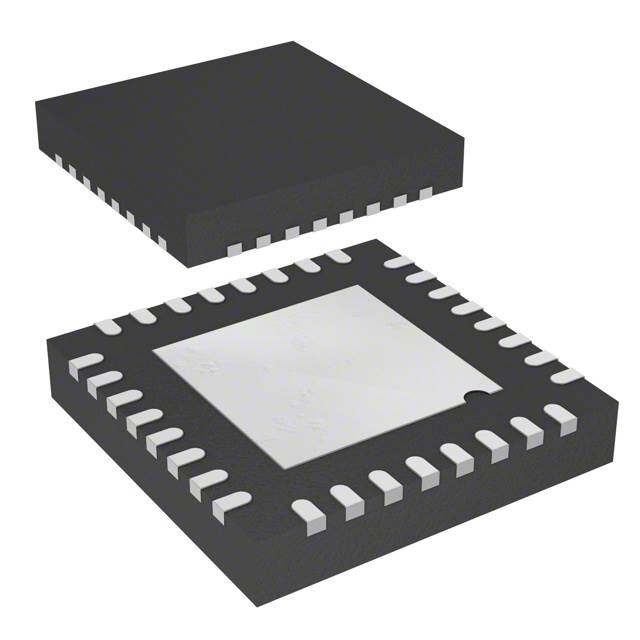
| 供应商器件封装 | 28-MLP-EP(5x5) |
| 其它名称 | 336-1271 |
| 包装 | 管件 |
| 单位重量 | 67.750 mg |
| 可用A/D通道 | 8 |
| 可编程输入/输出端数量 | 17 |
| 商标 | Silicon Labs |
| 处理器系列 | C8051 |
| 外设 | POR,PWM,温度传感器,WDT |
| 安装风格 | SMD/SMT |
| 定时器数量 | 16 Timer |
| 封装 | Tube |
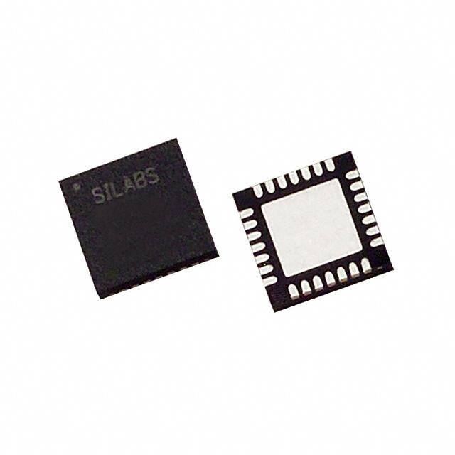
| 封装/外壳 | 28-VFQFN 裸露焊盘 |
| 封装/箱体 | QFN-28 |
| 工作温度 | -40°C ~ 85°C |
| 工作电源电压 | 2.7 V to 3.6 V |
| 工厂包装数量 | 73 |
| 振荡器类型 | 内部 |
| 接口类型 | I2C, SMBus, SPI, UART |
| 数据RAM大小 | 768 B |
| 数据ROM大小 | 128 B |
| 数据Rom类型 | Flash |
| 数据总线宽度 | 8 bit |
| 数据转换器 | A/D 8x24b; D/A 2x8b |
| 最大工作温度 | + 85 C |
| 最大时钟频率 | 50 MHz |
| 最小工作温度 | - 40 C |
| 标准包装 | 73 |
| 核心 | 8051 |
| 核心处理器 | 8051 |
| 核心尺寸 | 8-位 |
| 片上ADC | Yes |
| 片上DAC | With DAC |
| 电压-电源(Vcc/Vdd) | 2.7 V ~ 3.6 V |
| 电源电压-最大 | 3.6 V |
| 电源电压-最小 | 2.7 V |
| 程序存储器大小 | 8 kB |
| 程序存储器类型 | Flash闪存 |
| 程序存储容量 | 8KB(8K x 8) |
| 系列 | C8051F351 |
| 输入/输出端数量 | 17 I/O |
| 连接性 | SMBus(2 线/I²C), SPI, UART/USART |
| 速度 | 50MHz |
| 配用 | /product-detail/zh/C8051F350DK/336-1083-ND/656325 |


- 商务部:美国ITC正式对集成电路等产品启动337调查
- 曝三星4nm工艺存在良率问题 高通将骁龙8 Gen1或转产台积电
- 太阳诱电将投资9.5亿元在常州建新厂生产MLCC 预计2023年完工
- 英特尔发布欧洲新工厂建设计划 深化IDM 2.0 战略
- 台积电先进制程称霸业界 有大客户加持明年业绩稳了
- 达到5530亿美元!SIA预计今年全球半导体销售额将创下新高
- 英特尔拟将自动驾驶子公司Mobileye上市 估值或超500亿美元
- 三星加码芯片和SET,合并消费电子和移动部门,撤换高东真等 CEO
- 三星电子宣布重大人事变动 还合并消费电子和移动部门
- 海关总署:前11个月进口集成电路产品价值2.52万亿元 增长14.8%


PDF Datasheet 数据手册内容提取
C8051F350/1/2/3 8 k ISP Flash MCU Family Analog Peripherals High Speed 8051 µC Core - 24 or 16-Bit ADC - Pipelined Instruction architecture; executes 70% of • No missing codes instructions in 1 or 2 system clocks • 0.0015% nonlinearity - Up to 50 MIPS throughput • Programmable conversion rates up to 1 ksps • 8-Input multiplexer - Expanded interrupt handler • 1x to 128x PGA Memory • Built-in temperature sensor - Two 8-Bit Current Output DACs - 768 Bytes (256 + 512) On-Chip RAM - Comparator - 8 kB Flash; In-system programmable in 512-byte • Programmable hysteresis and response time Sectors • Configurable as interrupt or reset source Digital Peripherals • Low current (0.4 µA) On-chip Debug - 17 Port I/O; All 5 V tolerant with high sink current - On-chip debug circuitry facilitates full speed, non- - Enhanced UART, SMBus™, and SPI™ Serial Ports intrusive in-system debug (No emulator required) - Four general purpose 16-bit counter/timers - Provides breakpoints, single stepping, - 16-bit programmable counter array (PCA) with three inspect/modify memory and registers capture/compare modules - Superior performance to emulation systems using - Real time clock mode using PCA or timer and exter- ICE-Chips, target pods, and sockets nal clock source - Low Cost, Complete Development Kit Clock Sources Supply Voltage 2.7 to 3.6 V - Internal Oscillator: 24.5 MHz with ± 2% accuracy - Typical operating current: 5.8 mA @ 25 MHz; supports UART operation 11 µA @ 32 kHz - External Oscillator: Crystal, RC, C, or clock - Typical stop mode current: 0.1 µA (1 or 2 pin modes) Temperature Range: –40 to +85 °C - Clock multiplier to achieve 50 MHz internal clock - Can switch between clock sources on-the-fly 28-Pin QFN or 32-Pin LQFP Package - 5 x 5 mm PCB footprint with 28-QFN ANALOG DIGITAL I/O PERIPHERALS UART R A Port 0 8-bit SMBus B S A IDAC SPI S M 24/16-bit O 8-bit PCA R Port 1 U ADC C X IDAC Timer 0 + Timer 1 P2.0 TEMP - Timer 2 SENSOR VOLTAGE Timer 3 COMPARATOR 24.5 MHz PRECISION INTERNAL OSCILLATOR WITH CLOCK MULTIPLIER HIGH-SPEED CONTROLLER CORE 8 kB 8051 CPU 768 B SRAM ISP FLASH (50 MIPS) FLEXIBLE DEBUG POR WDT INTERRUPTS CIRCUITRY Rev. 1.1 5/07 Copyright © 2007 by Silicon Laboratories C8051F35x
C8051F350/1/2/3 NOTES: 2 Rev. 1.1
C8051F350/1/2/3 Table of Contents 1. System Overview.................................................................................................... 17 1.1. CIP-51™ Microcontroller................................................................................... 21 1.1.1. Fully 8051 Compatible Instruction Set...................................................... 21 1.1.2. Improved Throughput............................................................................... 21 1.1.3. Additional Features.................................................................................. 21 1.2. On-Chip Debug Circuitry................................................................................... 22 1.3. On-Chip Memory............................................................................................... 23 1.4. 24 or 16-Bit Analog to Digital Converter (ADC0).............................................. 24 1.5. Two 8-bit Current-Mode DACs.......................................................................... 25 1.6. Programmable Comparator.............................................................................. 26 1.7. Serial Ports....................................................................................................... 26 1.8. Port Input/Output............................................................................................... 27 1.9. Programmable Counter Array........................................................................... 28 2. Absolute Maximum Ratings.................................................................................. 29 3. Global DC Electrical Characteristics.................................................................... 30 4. Pinout and Package Definitions............................................................................ 31 5. 24 or 16-Bit Analog to Digital Converter (ADC0)................................................. 41 5.1. Configuration..................................................................................................... 42 5.1.1. Voltage Reference Selection.................................................................... 42 5.1.2. Analog Inputs........................................................................................... 42 5.1.3. Modulator Clock....................................................................................... 43 5.1.4. Decimation Ratio...................................................................................... 43 5.2. Calibrating the ADC.......................................................................................... 44 5.2.1. Internal Calibration................................................................................... 44 5.2.2. System Calibration................................................................................... 44 5.2.3. Calibration Coefficient Storage................................................................. 44 5.3. Performing Conversions................................................................................... 46 5.3.1. Single Conversions.................................................................................. 46 5.3.2. Continuous Conversions.......................................................................... 46 5.3.3. ADC Output.............................................................................................. 46 5.3.4. Error Conditions....................................................................................... 47 5.4. Offset DAC........................................................................................................ 47 5.5. Burnout Current Sources.................................................................................. 47 5.6. Analog Multiplexer............................................................................................ 59 6. 8-Bit Current Mode DACS (IDA0 and IDA1).......................................................... 67 6.1. IDAC Output Scheduling................................................................................... 68 6.1.1. Update Output On-Demand..................................................................... 68 6.1.2. Update Output Based on Timer Overflow................................................ 68 6.1.3. Update Output Based on CNVSTR Edge................................................. 68 6.2. IDAC Output Mapping....................................................................................... 68 6.3. IDAC External Pin Connections........................................................................ 71 7. Voltage Reference.................................................................................................. 73 8. Temperature Sensor............................................................................................... 77 Rev. 1.1 3
C8051F350/1/2/3 9. Comparator0........................................................................................................... 79 9.1. Comparator0 Inputs and Outputs...................................................................... 83 10.CIP-51 Microcontroller........................................................................................... 87 10.1.Instruction Set................................................................................................... 89 10.1.1.Instruction and CPU Timing..................................................................... 89 10.1.2.MOVX Instruction and Program Memory................................................. 89 10.2.Register Descriptions....................................................................................... 93 10.3.Power Management Modes.............................................................................. 96 10.3.1.Idle Mode................................................................................................. 96 10.3.2.Stop Mode................................................................................................ 96 11.Memory Organization and SFRs........................................................................... 99 11.1.Program Memory.............................................................................................. 99 11.2.Data Memory.................................................................................................. 100 11.3.General Purpose Registers............................................................................ 100 11.4.Bit Addressable Locations.............................................................................. 100 11.5.Stack............................................................................................................... 100 11.6.Special Function Registers............................................................................. 101 12.Interrupt Handler.................................................................................................. 105 12.1.MCU Interrupt Sources and Vectors............................................................... 105 12.2.Interrupt Priorities........................................................................................... 105 12.3.Interrupt Latency............................................................................................. 105 12.4.Interrupt Register Descriptions....................................................................... 107 12.5.External Interrupts.......................................................................................... 111 13.Prefetch Engine.................................................................................................... 113 14.Reset Sources....................................................................................................... 115 14.1.Power-On Reset............................................................................................. 116 14.2.Power-Fail Reset / VDD Monitor.................................................................... 117 14.3.External Reset................................................................................................ 118 14.4.Missing Clock Detector Reset........................................................................ 118 14.5.Comparator0 Reset........................................................................................ 118 14.6.PCA Watchdog Timer Reset.......................................................................... 118 14.7.Flash Error Reset........................................................................................... 118 14.8.Software Reset............................................................................................... 118 15.Flash Memory....................................................................................................... 121 15.1.Programming The Flash Memory................................................................... 121 15.1.1.Flash Lock and Key Functions............................................................... 121 15.1.2.Flash Erase Procedure.......................................................................... 121 15.1.3.Flash Write Procedure........................................................................... 122 15.2.Non-volatile Data Storage.............................................................................. 123 15.3.Security Options............................................................................................. 123 16.External RAM........................................................................................................ 127 17.Oscillators............................................................................................................. 129 17.1.Programmable Internal Oscillator................................................................... 129 17.2.External Oscillator Drive Circuit...................................................................... 131 17.2.1.Clocking Timers Directly Through the External Oscillator...................... 131 4 Rev. 1.1
C8051F350/1/2/3 17.2.2.External Crystal Example....................................................................... 131 17.2.3.External RC Example............................................................................. 133 17.2.4.External Capacitor Example................................................................... 133 17.3.Clock Multiplier............................................................................................... 135 17.4.System Clock Selection.................................................................................. 136 18.Port Input/Output.................................................................................................. 137 18.1.Priority Crossbar Decoder.............................................................................. 139 18.2.Port I/O Initialization....................................................................................... 141 18.3.General Purpose Port I/O............................................................................... 144 19.SMBus................................................................................................................... 151 19.1.Supporting Documents................................................................................... 152 19.2.SMBus Configuration...................................................................................... 152 19.3.SMBus Operation........................................................................................... 152 19.3.1.Arbitration............................................................................................... 153 19.3.2.Clock Low Extension.............................................................................. 154 19.3.3.SCL Low Timeout................................................................................... 154 19.3.4.SCL High (SMBus Free) Timeout.......................................................... 154 19.4.Using the SMBus............................................................................................ 155 19.4.1.SMBus Configuration Register............................................................... 156 19.4.2.SMB0CN Control Register..................................................................... 159 19.4.3.Data Register......................................................................................... 162 19.5.SMBus Transfer Modes.................................................................................. 163 19.5.1.Master Transmitter Mode....................................................................... 163 19.5.2.Master Receiver Mode........................................................................... 164 19.5.3.Slave Receiver Mode............................................................................. 165 19.5.4.Slave Transmitter Mode......................................................................... 166 19.6.SMBus Status Decoding................................................................................. 167 20.UART0.................................................................................................................... 171 20.1.Enhanced Baud Rate Generation................................................................... 172 20.2.Operational Modes......................................................................................... 173 20.2.1.8-Bit UART............................................................................................. 173 20.2.2.9-Bit UART............................................................................................. 174 20.3.Multiprocessor Communications.................................................................... 174 21.Serial Peripheral Interface (SPI0)........................................................................ 181 21.1.Signal Descriptions......................................................................................... 182 21.1.1.Master Out, Slave In (MOSI).................................................................. 182 21.1.2.Master In, Slave Out (MISO).................................................................. 182 21.1.3.Serial Clock (SCK)................................................................................. 182 21.1.4.Slave Select (NSS)................................................................................ 182 21.2.SPI0 Master Mode Operation......................................................................... 183 21.3.SPI0 Slave Mode Operation........................................................................... 185 21.4.SPI0 Interrupt Sources................................................................................... 185 21.5.Serial Clock Timing......................................................................................... 186 21.6.SPI Special Function Registers...................................................................... 186 Rev. 1.1 5
C8051F350/1/2/3 22.Timers.................................................................................................................... 195 22.1.Timer 0 and Timer 1....................................................................................... 195 22.1.1.Mode 0: 13-bit Counter/Timer................................................................ 195 22.1.2.Mode 1: 16-bit Counter/Timer................................................................ 196 22.1.3.Mode 2: 8-bit Counter/Timer with Auto-Reload...................................... 197 22.1.4.Mode 3: Two 8-bit Counter/Timers (Timer 0 Only)................................. 198 22.2.Timer 2 .......................................................................................................... 203 22.2.1.16-bit Timer with Auto-Reload................................................................ 203 22.2.2.8-bit Timers with Auto-Reload................................................................ 204 22.3.Timer 3 .......................................................................................................... 207 22.3.1.16-bit Timer with Auto-Reload................................................................ 207 22.3.2.8-bit Timers with Auto-Reload................................................................ 208 23.Programmable Counter Array............................................................................. 211 23.1.PCA Counter/Timer........................................................................................ 212 23.2.Capture/Compare Modules............................................................................ 213 23.2.1.Edge-triggered Capture Mode................................................................ 214 23.2.2.Software Timer (Compare) Mode........................................................... 215 23.2.3.High Speed Output Mode....................................................................... 216 23.2.4.Frequency Output Mode........................................................................ 217 23.2.5.8-Bit Pulse Width Modulator Mode......................................................... 218 23.2.6.16-Bit Pulse Width Modulator Mode....................................................... 219 23.3.Watchdog Timer Mode................................................................................... 220 23.3.1.Watchdog Timer Operation.................................................................... 220 23.3.2.Watchdog Timer Usage......................................................................... 221 23.4.Register Descriptions for PCA........................................................................ 222 24.Revision Specific Behavior................................................................................. 227 24.1.Revision Identification..................................................................................... 227 25.C2 Interface........................................................................................................... 229 25.1.C2 Interface Registers.................................................................................... 229 25.2.C2 Pin Sharing............................................................................................... 231 Document Change List............................................................................................. 232 Contact Information.................................................................................................. 234 6 Rev. 1.1
C8051F350/1/2/3 List of Figures 1. System Overview Figure 1.1. C8051F350 Block Diagram.................................................................... 19 Figure 1.2. C8051F351 Block Diagram.................................................................... 19 Figure 1.3. C8051F352 Block Diagram.................................................................... 20 Figure 1.4. C8051F353 Block Diagram.................................................................... 20 Figure 1.5. Development/In-System Debug Diagram............................................... 22 Figure 1.6. Memory Map.......................................................................................... 23 Figure 1.7. ADC0 Block Diagram............................................................................. 24 Figure 1.8. IDAC Block Diagram.............................................................................. 25 Figure 1.9. Comparator0 Block Diagram.................................................................. 26 Figure 1.10. Port I/O Functional Block Diagram....................................................... 27 Figure 1.11. PCA Block Diagram.............................................................................. 28 2. Absolute Maximum Ratings 3. Global DC Electrical Characteristics 4. Pinout and Package Definitions Figure 4.1. LQFP-32 Pinout Diagram (Top View).................................................... 34 Figure 4.2. QFN-28 Pinout Diagram (Top View)...................................................... 35 Figure 4.3. LQFP-32 Package Diagram................................................................... 36 Figure 4.4. QFN-28 Package Drawing..................................................................... 37 Figure 4.5. Typical QFN-28 Landing Diagram.......................................................... 38 Figure 4.6. Typical QFN-28 Solder Paste Diagram.................................................. 39 5. 24 or 16-Bit Analog to Digital Converter (ADC0) Figure 5.1. ADC0 Block Diagram............................................................................. 41 Figure 5.2. ADC0 Buffer Control.............................................................................. 43 Figure 5.3. ADC0 Offset Calibration Register Coding.............................................. 45 Figure 5.4. ADC0 Gain Calibration Register Coding................................................ 45 Figure 5.5. ADC0 Multiplexer Connections.............................................................. 59 6. 8-Bit Current Mode DACS (IDA0 and IDA1) Figure 6.1. IDAC Functional Block Diagram............................................................. 67 Figure 6.2. IDAC Data Word Mapping...................................................................... 68 Figure 6.3. IDAC Pin Connections........................................................................... 71 7. Voltage Reference Figure 7.1. Reference Circuitry Block Diagram........................................................ 73 8. Temperature Sensor Figure 8.1. Temperature Sensor Block Diagram...................................................... 77 Figure 8.2. Single Channel Transfer Function.......................................................... 78 Figure 8.3. Differential Transfer Function................................................................. 78 9. Comparator0 Figure 9.1. Comparator0 Functional Block Diagram................................................ 79 Figure 9.2. Comparator Hysteresis Plot................................................................... 80 Figure 9.3. Comparator Pin Connections................................................................. 83 10.CIP-51 Microcontroller Figure 10.1. CIP-51 Block Diagram.......................................................................... 87 Rev. 1.1 7
C8051F350/1/2/3 11.Memory Organization and SFRs Figure 11.1. Memory Map........................................................................................ 99 12.Interrupt Handler 13.Prefetch Engine 14.Reset Sources Figure 14.1. Reset Sources.................................................................................... 115 Figure 14.2. Power-On and VDD Monitor Reset Timing........................................ 116 15.Flash Memory Figure 15.1. Flash Memory Map............................................................................. 123 16.External RAM 17.Oscillators Figure 17.1. Oscillator Diagram.............................................................................. 129 Figure 17.2. 32.768 kHz External Crystal Example................................................ 132 18.Port Input/Output Figure 18.1. Port I/O Functional Block Diagram..................................................... 137 Figure 18.2. Port I/O Cell Block Diagram............................................................... 138 Figure 18.3. Crossbar Priority Decoder with No Pins Skipped............................... 139 Figure 18.4. Crossbar Priority Decoder with Crystal Pins Skipped........................ 140 19.SMBus Figure 19.1. SMBus Block Diagram....................................................................... 151 Figure 19.2. Typical SMBus Configuration............................................................. 152 Figure 19.3. SMBus Transaction............................................................................ 153 Figure 19.4. Typical SMBus SCL Generation......................................................... 157 Figure 19.5. Typical Master Transmitter Sequence................................................ 163 Figure 19.6. Typical Master Receiver Sequence.................................................... 164 Figure 19.7. Typical Slave Receiver Sequence...................................................... 165 Figure 19.8. Typical Slave Transmitter Sequence.................................................. 166 20.UART0 Figure 20.1. UART0 Block Diagram....................................................................... 171 Figure 20.2. UART0 Baud Rate Logic.................................................................... 172 Figure 20.3. UART Interconnect Diagram.............................................................. 173 Figure 20.4. 8-Bit UART Timing Diagram............................................................... 173 Figure 20.5. 9-Bit UART Timing Diagram............................................................... 174 Figure 20.6. UART Multi-Processor Mode Interconnect Diagram.......................... 175 21.Serial Peripheral Interface (SPI0) Figure 21.1. SPI Block Diagram............................................................................. 181 Figure 21.2. Multiple-Master Mode Connection Diagram....................................... 184 Figure 21.3. 3-Wire Single Master and Slave Mode Connection Diagram............. 184 Figure 21.4. 4-Wire Single Master and Slave Mode Connection Diagram............. 184 Figure 21.5. Data/Clock Timing Relationship......................................................... 186 Figure 21.6. SPI Master Timing (CKPHA = 0)........................................................ 191 Figure 21.7. SPI Master Timing (CKPHA = 1)........................................................ 191 Figure 21.8. SPI Slave Timing (CKPHA = 0).......................................................... 192 Figure 21.9. SPI Slave Timing (CKPHA = 1).......................................................... 192 8 Rev. 1.1
C8051F350/1/2/3 22.Timers Figure 22.1. T0 Mode 0 Block Diagram.................................................................. 196 Figure 22.2. T0 Mode 2 Block Diagram.................................................................. 197 Figure 22.3. T0 Mode 3 Block Diagram.................................................................. 198 Figure 22.4. Timer 2 16-Bit Mode Block Diagram.................................................. 203 Figure 22.5. Timer 2 8-Bit Mode Block Diagram.................................................... 204 Figure 22.6. Timer 3 16-Bit Mode Block Diagram.................................................. 207 Figure 22.7. Timer 3 8-Bit Mode Block Diagram.................................................... 208 23.Programmable Counter Array Figure 23.1. PCA Block Diagram............................................................................ 211 Figure 23.2. PCA Counter/Timer Block Diagram.................................................... 212 Figure 23.3. PCA Interrupt Block Diagram............................................................. 213 Figure 23.4. PCA Capture Mode Diagram.............................................................. 214 Figure 23.5. PCA Software Timer Mode Diagram.................................................. 215 Figure 23.6. PCA High Speed Output Mode Diagram............................................ 216 Figure 23.7. PCA Frequency Output Mode............................................................ 217 Figure 23.8. PCA 8-Bit PWM Mode Diagram......................................................... 218 Figure 23.9. PCA 16-Bit PWM Mode...................................................................... 219 Figure 23.10. PCA Module 2 with Watchdog Timer Enabled................................. 220 24.Revision Specific Behavior Figure 24.1. Reading Package Marking................................................................. 227 25.C2 Interface Figure 25.1. Typical C2 Pin Sharing....................................................................... 231 Rev. 1.1 9
C8051F350/1/2/3 NOTES: 10 Rev. 1.1
C8051F350/1/2/3 List of Tables 1. System Overview Table 1.1. Product Selection Guide ......................................................................... 18 2. Absolute Maximum Ratings 3. Global DC Electrical Characteristics 4. Pinout and Package Definitions Table 4.1. Pin Definitions for the C8051F350/1/2/3 ................................................. 31 Table 4.2. LQFP-32 Package Dimensions .............................................................. 36 Table 4.3. QFN-28 Package Dimensions ................................................................ 37 5. 24 or 16-Bit Analog to Digital Converter (ADC0) Table 5.1. ADC0 Unipolar Output Word Coding (AD0POL = 0) .............................. 47 Table 5.2. ADC0 Bipolar Output Word Coding (AD0POL = 1) ................................ 47 Table 5.3. ADC0 SINC3 Filter Typical RMS Noise (µV) .......................................... 62 Table 5.4. ADC0 SINC3 Filter Effective Resolution in Unipolar Mode (bits) ......................................................................... 63 Table 5.5. ADC0 SINC3 Filter Flicker-Free (Noise-Free) Resolution in Unipolar Mode (bits) ......................................................................... 63 Table 5.6. ADC0 Fast Filter Typical RMS Noise (µV) ............................................. 64 Table 5.7. ADC0 Fast Filter Effective Resolution1 in Unipolar Mode (bits) ............. 64 Table 5.8. ADC0 Fast Filter Flicker-Free (Noise-Free) Resolution in Unipolar Mode (bits) ......................................................................... 65 6. 8-Bit Current Mode DACS (IDA0 and IDA1) 7. Voltage Reference 8. Temperature Sensor 9. Comparator0 10.CIP-51 Microcontroller Table 10.1. CIP-51 Instruction Set Summary .......................................................... 89 11.Memory Organization and SFRs Table 11.1. Special Function Register (SFR) Memory Map .................................. 101 Table 11.2. Special Function Registers ................................................................. 102 12.Interrupt Handler Table 12.1. Interrupt Summary .............................................................................. 106 13.Prefetch Engine 14.Reset Sources 15.Flash Memory 16.External RAM 17.Oscillators 18.Port Input/Output 19.SMBus Table 19.1. SMBus Clock Source Selection .......................................................... 156 Table 19.2. Minimum SDA Setup and Hold Times ................................................ 157 Table 19.3. Sources for Hardware Changes to SMB0CN ..................................... 161 Table 19.4. SMBus Status Decoding ..................................................................... 167 20.UART0 Rev. 1.1 11
C8051F350/1/2/3 Table 20.1. Timer Settings for Standard Baud Rates Using the Internal Oscillator ............................................................... 178 Table 20.2. Timer Settings for Standard Baud Rates Using an External 25.0 MHz Oscillator ............................................... 178 Table 20.3. Timer Settings for Standard Baud Rates Using an External 22.1184 MHz Oscillator ......................................... 179 Table 20.4. Timer Settings for Standard Baud Rates Using an External 18.432 MHz Oscillator ........................................... 179 Table 20.5. Timer Settings for Standard Baud Rates Using an External 11.0592 MHz Oscillator ......................................... 180 Table 20.6. Timer Settings for Standard Baud Rates Using an External 3.6864 MHz Oscillator ........................................... 180 21.Serial Peripheral Interface (SPI0) Table 21.1. SPI Slave Timing Parameters ............................................................ 193 22.Timers 23.Programmable Counter Array Table 23.1. PCA Timebase Input Options ............................................................. 212 Table 23.2. PCA0CPM Register Settings for PCA Capture/Compare Modules .... 213 Table 23.3. Watchdog Timer Timeout Intervals...................................................... 221 24.Revision Specific Behavior 25.C2 Interface 12 Rev. 1.1
C8051F350/1/2/3 List of Registers SFR Definition 5.1. ADC0CN: ADC0 Control . . . . . . . . . . . . . . . . . . . . . . . . . . . . . . . . 48 SFR Definition 5.2. ADC0CF: ADC0 Configuration . . . . . . . . . . . . . . . . . . . . . . . . . . . 49 SFR Definition 5.3. ADC0MD: ADC0 Mode . . . . . . . . . . . . . . . . . . . . . . . . . . . . . . . . . 50 SFR Definition 5.4. ADC0CLK: ADC0 Modulator Clock Divisor . . . . . . . . . . . . . . . . . . 51 SFR Definition 5.5. ADC0DECH: ADC0 Decimation Ratio Register High Byte . . . . . . 51 SFR Definition 5.6. ADC0DECL: ADC0 Decimation Ratio Register Low Byte . . . . . . . 52 SFR Definition 5.7. ADC0DAC: ADC0 Offset DAC . . . . . . . . . . . . . . . . . . . . . . . . . . . . 52 SFR Definition 5.8. ADC0BUF: ADC0 Input Buffer Control . . . . . . . . . . . . . . . . . . . . . 53 SFR Definition 5.9. ADC0STA: ADC0 Status . . . . . . . . . . . . . . . . . . . . . . . . . . . . . . . . 54 SFR Definition 5.10. ADC0COH: ADC0 Offset Calibration Register High Byte . . . . . . 55 SFR Definition 5.11. ADC0COM: ADC0 Offset Calibration Register Middle Byte . . . . 55 SFR Definition 5.12. ADC0COL: ADC0 Offset Calibration Register Low Byte . . . . . . . 55 SFR Definition 5.13. ADC0CGH: ADC0 Gain Calibration Register High Byte . . . . . . . 56 SFR Definition 5.14. ADC0CGM: ADC0 Gain Calibration Register Middle Byte . . . . . 56 SFR Definition 5.15. ADC0CGL: ADC0 Gain Calibration Register Low Byte . . . . . . . . 56 SFR Definition 5.16. ADC0H: ADC0 Conversion Register (SINC3 Filter) High Byte . . 57 SFR Definition 5.17. ADC0M: ADC0 Conversion Register (SINC3 Filter) Middle Byte 57 SFR Definition 5.18. ADC0L: ADC0 Conversion Register (SINC3 Filter) Low Byte . . . 57 SFR Definition 5.19. ADC0FH: ADC0 Conversion Register (Fast Filter) High Byte . . . 58 SFR Definition 5.20. ADC0FM: ADC0 Conversion Register (Fast Filter) Middle Byte . 58 SFR Definition 5.21. ADC0FL: ADC0 Conversion Register (Fast Filter) Low Byte . . . . 58 SFR Definition 5.22. ADC0MUX: ADC0 Analog Multiplexer Control . . . . . . . . . . . . . . 60 SFR Definition 6.1. IDA0CN: IDA0 Control . . . . . . . . . . . . . . . . . . . . . . . . . . . . . . . . . . 69 SFR Definition 6.2. IDA0: IDA0 Data Word . . . . . . . . . . . . . . . . . . . . . . . . . . . . . . . . . . 69 SFR Definition 6.3. IDA1CN: IDA1 Control . . . . . . . . . . . . . . . . . . . . . . . . . . . . . . . . . 70 SFR Definition 6.4. IDA1: IDA1 Data Word . . . . . . . . . . . . . . . . . . . . . . . . . . . . . . . . . . 70 SFR Definition 7.1. REF0CN: Reference Control . . . . . . . . . . . . . . . . . . . . . . . . . . . . . 74 SFR Definition 9.1. CPT0CN: Comparator0 Control . . . . . . . . . . . . . . . . . . . . . . . . . . . 81 SFR Definition 9.2. CPT0MD: Comparator0 Mode Selection . . . . . . . . . . . . . . . . . . . . 82 SFR Definition 9.3. CPT0MX: Comparator0 MUX Selection . . . . . . . . . . . . . . . . . . . . 84 SFR Definition 10.1. SP: Stack Pointer . . . . . . . . . . . . . . . . . . . . . . . . . . . . . . . . . . . . . 93 SFR Definition 10.2. DPL: Data Pointer Low Byte . . . . . . . . . . . . . . . . . . . . . . . . . . . . 93 SFR Definition 10.3. DPH: Data Pointer High Byte . . . . . . . . . . . . . . . . . . . . . . . . . . . 93 SFR Definition 10.4. PSW: Program Status Word . . . . . . . . . . . . . . . . . . . . . . . . . . . . 94 SFR Definition 10.5. ACC: Accumulator . . . . . . . . . . . . . . . . . . . . . . . . . . . . . . . . . . . . 95 SFR Definition 10.6. B: B Register . . . . . . . . . . . . . . . . . . . . . . . . . . . . . . . . . . . . . . . . 95 SFR Definition 10.7. PCON: Power Control . . . . . . . . . . . . . . . . . . . . . . . . . . . . . . . . . 97 SFR Definition 12.1. IE: Interrupt Enable . . . . . . . . . . . . . . . . . . . . . . . . . . . . . . . . . . 107 SFR Definition 12.2. IP: Interrupt Priority . . . . . . . . . . . . . . . . . . . . . . . . . . . . . . . . . . 108 SFR Definition 12.3. EIE1: Extended Interrupt Enable 1 . . . . . . . . . . . . . . . . . . . . . . 109 SFR Definition 12.4. EIP1: Extended Interrupt Priority 1 . . . . . . . . . . . . . . . . . . . . . . 110 SFR Definition 12.5. IT01CF: INT0/INT1 Configuration . . . . . . . . . . . . . . . . . . . . . . . 112 SFR Definition 13.1. PFE0CN: Prefetch Engine Control . . . . . . . . . . . . . . . . . . . . . . 113 Rev. 1.1 13
C8051F350/1/2/3 SFR Definition 14.1. VDM0CN: VDD Monitor Control . . . . . . . . . . . . . . . . . . . . . . . . 117 SFR Definition 14.2. RSTSRC: Reset Source . . . . . . . . . . . . . . . . . . . . . . . . . . . . . . 119 SFR Definition 15.1. PSCTL: Program Store R/W Control . . . . . . . . . . . . . . . . . . . . . 125 SFR Definition 15.2. FLKEY: Flash Lock and Key . . . . . . . . . . . . . . . . . . . . . . . . . . . 125 SFR Definition 15.3. FLSCL: Flash Scale . . . . . . . . . . . . . . . . . . . . . . . . . . . . . . . . . . 126 SFR Definition 16.1. EMI0CN: External Memory Interface Control . . . . . . . . . . . . . . 127 SFR Definition 17.1. OSCICN: Internal Oscillator Control . . . . . . . . . . . . . . . . . . . . . 130 SFR Definition 17.2. OSCICL: Internal Oscillator Calibration . . . . . . . . . . . . . . . . . . . 130 SFR Definition 17.3. OSCXCN: External Oscillator Control . . . . . . . . . . . . . . . . . . . . 134 SFR Definition 17.4. CLKMUL: Clock Multiplier Control . . . . . . . . . . . . . . . . . . . . . . . 135 SFR Definition 17.5. CLKSEL: Clock Select . . . . . . . . . . . . . . . . . . . . . . . . . . . . . . . . 136 SFR Definition 18.1. XBR0: Port I/O Crossbar Register 0 . . . . . . . . . . . . . . . . . . . . . 142 SFR Definition 18.2. XBR1: Port I/O Crossbar Register 1 . . . . . . . . . . . . . . . . . . . . . 143 SFR Definition 18.3. P0: Port0 . . . . . . . . . . . . . . . . . . . . . . . . . . . . . . . . . . . . . . . . . . 145 SFR Definition 18.4. P0MDIN: Port0 Input Mode . . . . . . . . . . . . . . . . . . . . . . . . . . . . 145 SFR Definition 18.5. P0MDOUT: Port0 Output Mode . . . . . . . . . . . . . . . . . . . . . . . . . 146 SFR Definition 18.6. P0SKIP: Port0 Skip . . . . . . . . . . . . . . . . . . . . . . . . . . . . . . . . . . 146 SFR Definition 18.7. P1: Port1 . . . . . . . . . . . . . . . . . . . . . . . . . . . . . . . . . . . . . . . . . . 147 SFR Definition 18.8. P1MDIN: Port1 Input Mode . . . . . . . . . . . . . . . . . . . . . . . . . . . . 147 SFR Definition 18.9. P1MDOUT: Port1 Output Mode . . . . . . . . . . . . . . . . . . . . . . . . . 148 SFR Definition 18.10. P1SKIP: Port1 Skip . . . . . . . . . . . . . . . . . . . . . . . . . . . . . . . . . 148 SFR Definition 18.11. P2: Port2 . . . . . . . . . . . . . . . . . . . . . . . . . . . . . . . . . . . . . . . . . 149 SFR Definition 18.12. P2MDOUT: Port2 Output Mode . . . . . . . . . . . . . . . . . . . . . . . . 149 SFR Definition 19.1. SMB0CF: SMBus Clock/Configuration . . . . . . . . . . . . . . . . . . . 158 SFR Definition 19.2. SMB0CN: SMBus Control . . . . . . . . . . . . . . . . . . . . . . . . . . . . . 160 SFR Definition 19.3. SMB0DAT: SMBus Data . . . . . . . . . . . . . . . . . . . . . . . . . . . . . . 162 SFR Definition 20.1. SCON0: Serial Port 0 Control . . . . . . . . . . . . . . . . . . . . . . . . . . 176 SFR Definition 20.2. SBUF0: Serial (UART0) Port Data Buffer . . . . . . . . . . . . . . . . . 177 SFR Definition 21.1. SPI0CFG: SPI0 Configuration . . . . . . . . . . . . . . . . . . . . . . . . . . 187 SFR Definition 21.2. SPI0CN: SPI0 Control . . . . . . . . . . . . . . . . . . . . . . . . . . . . . . . . 188 SFR Definition 21.3. SPI0CKR: SPI0 Clock Rate . . . . . . . . . . . . . . . . . . . . . . . . . . . . 189 SFR Definition 21.4. SPI0DAT: SPI0 Data . . . . . . . . . . . . . . . . . . . . . . . . . . . . . . . . . 190 SFR Definition 22.1. TCON: Timer Contro . . . . . . . . . . . . . . . . . . . . . . . . . . . . . . . . . 199 SFR Definition 22.2. TMOD: Timer Mode . . . . . . . . . . . . . . . . . . . . . . . . . . . . . . . . . . 200 SFR Definition 22.3. CKCON: Clock Control . . . . . . . . . . . . . . . . . . . . . . . . . . . . . . . 201 SFR Definition 22.4. TL0: Timer 0 Low Byte . . . . . . . . . . . . . . . . . . . . . . . . . . . . . . . . 202 SFR Definition 22.5. TL1: Timer 1 Low Byte . . . . . . . . . . . . . . . . . . . . . . . . . . . . . . . . 202 SFR Definition 22.6. TH0: Timer 0 High Byte . . . . . . . . . . . . . . . . . . . . . . . . . . . . . . . 202 SFR Definition 22.7. TH1: Timer 1 High Byte . . . . . . . . . . . . . . . . . . . . . . . . . . . . . . . 202 SFR Definition 22.8. TMR2CN: Timer 2 Control . . . . . . . . . . . . . . . . . . . . . . . . . . . . . 205 SFR Definition 22.9. TMR2RLL: Timer 2 Reload Register Low Byte . . . . . . . . . . . . . 206 SFR Definition 22.10. TMR2RLH: Timer 2 Reload Register High Byte . . . . . . . . . . . 206 SFR Definition 22.11. TMR2L: Timer 2 Low Byte . . . . . . . . . . . . . . . . . . . . . . . . . . . . 206 SFR Definition 22.12. TMR2H Timer 2 High Byte . . . . . . . . . . . . . . . . . . . . . . . . . . . . 206 SFR Definition 22.13. TMR3CN: Timer 3 Control . . . . . . . . . . . . . . . . . . . . . . . . . . . . 209 14 Rev. 1.1
C8051F350/1/2/3 SFR Definition 22.14. TMR3RLL: Timer 3 Reload Register Low Byte . . . . . . . . . . . . 210 SFR Definition 22.15. TMR3RLH: Timer 3 Reload Register High Byte . . . . . . . . . . . 210 SFR Definition 22.16. TMR3L: Timer 3 Low Byte . . . . . . . . . . . . . . . . . . . . . . . . . . . . 210 SFR Definition 22.17. TMR3H Timer 3 High Byte . . . . . . . . . . . . . . . . . . . . . . . . . . . . 210 SFR Definition 23.1. PCA0CN: PCA Control . . . . . . . . . . . . . . . . . . . . . . . . . . . . . . . 222 SFR Definition 23.2. PCA0MD: PCA Mode . . . . . . . . . . . . . . . . . . . . . . . . . . . . . . . . 223 SFR Definition 23.3. PCA0CPMn: PCA Capture/Compare Mode . . . . . . . . . . . . . . . 224 SFR Definition 23.4. PCA0L: PCA Counter/Timer Low Byte . . . . . . . . . . . . . . . . . . . 225 SFR Definition 23.5. PCA0H: PCA Counter/Timer High Byte . . . . . . . . . . . . . . . . . . . 225 SFR Definition 23.6. PCA0CPLn: PCA Capture Module Low Byte . . . . . . . . . . . . . . . 226 SFR Definition 23.7. PCA0CPHn: PCA Capture Module High Byte . . . . . . . . . . . . . . 226 C2 Register Definition 25.1. C2ADD: C2 Address . . . . . . . . . . . . . . . . . . . . . . . . . . . 229 C2 Register Definition 25.2. DEVICEID: C2 Device ID . . . . . . . . . . . . . . . . . . . . . . . . 229 C2 Register Definition 25.3. REVID: C2 Revision ID . . . . . . . . . . . . . . . . . . . . . . . . . 230 C2 Register Definition 25.4. FPCTL: C2 Flash Programming Control . . . . . . . . . . . . 230 C2 Register Definition 25.5. FPDAT: C2 Flash Programming Data . . . . . . . . . . . . . . 230 Rev. 1.1 15
C8051F350/1/2/3 NOTES: 16 Rev. 1.1
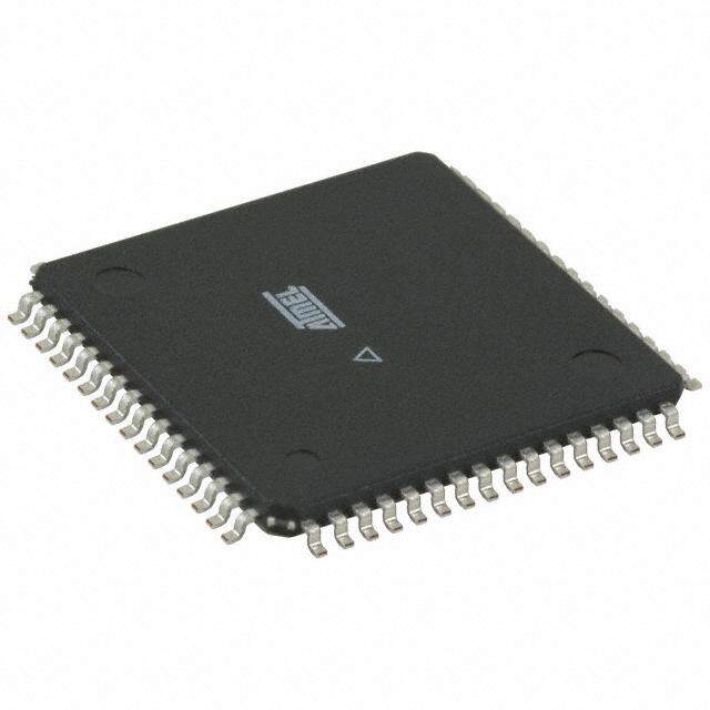
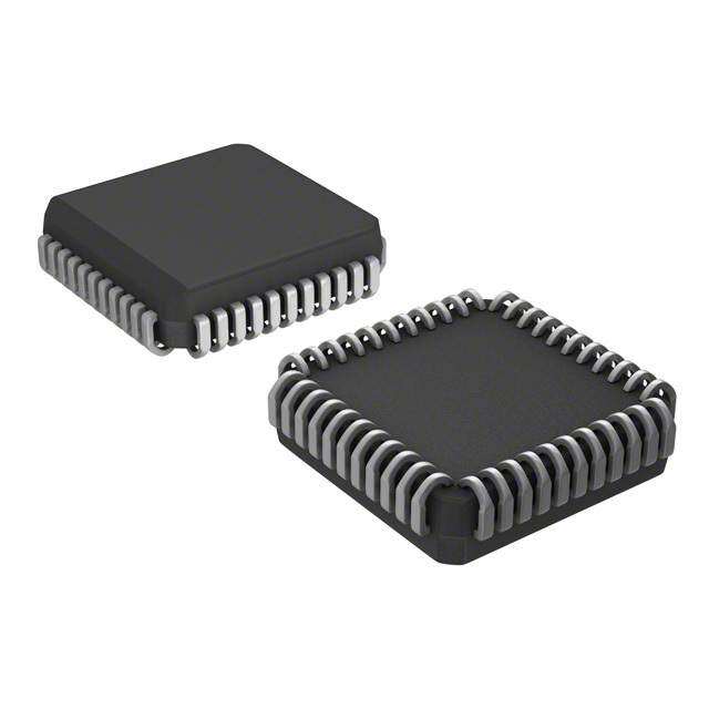
C8051F350/1/2/3 1. System Overview C8051F350/1/2/3 devices are fully integrated mixed-signal System-on-a-Chip MCUs. Highlighted features are listed below. Refer to Table 1.1 for specific product feature selection. • High-speed pipelined 8051-compatible microcontroller core (up to 50 MIPS) • In-system, full-speed, non-intrusive debug interface (on-chip) • 24 or 16-bit single-ended/differential ADC with analog multiplexer • Two 8-bit Current Output DACs • Precision programmable 24.5 MHz internal oscillator • 8 kB of on-chip Flash memory • 768 bytes of on-chip RAM • SMBus/I2C, Enhanced UART, and SPI serial interfaces implemented in hardware • Four general-purpose 16-bit timers • Programmable counter/timer array (PCA) with three capture/compare modules and watchdog timer function • On-chip power-on reset, V monitor, and temperature sensor DD • On-chip voltage comparator • 17 Port I/O (5 V tolerant) With on-chip power-on reset, V monitor, watchdog timer, and clock oscillator, the C8051F350/1/2/3 DD devices are truly stand-alone System-on-a-Chip solutions. The Flash memory can be reprogrammed even in-circuit, providing non-volatile data storage, and also allowing field upgrades of the 8051 firmware. User software has complete control of all peripherals, and may individually shut down any or all peripherals for power savings. The on-chip Silicon Labs 2-Wire (C2) Development Interface allows non-intrusive (uses no on-chip resources), full speed, in-circuit debugging using the production MCU installed in the final application. This debug logic supports inspection and modification of memory and registers, setting breakpoints, single stepping, run and halt commands. All analog and digital peripherals are fully functional while debugging using C2. The two C2 interface pins can be shared with user functions, allowing in-system debugging with- out occupying package pins. Each device is specified for 2.7 to 3.6 V operation over the industrial temperature range (–45 to +85 °C). The Port I/O and /RST pins are tolerant of input signals up to 5 V. The C8051F350/1/2/3 are available in 28-pin QFN (also referred to as MLP or MLF) or 32-pin LQFP packaging, as shown in Figure 1.1 through Figure 1.4. Rev. 1.1 17
C8051F350/1/2/3 Table 1.1. Product Selection Guide r o at cill s O s Ordering Part Number MIPS (Peak) Flash Memory RAM Calibrated Internal 24.5 MHz Clock Multiplier SMBus/I2C SPI UART Timers (16-bit) Programmable Counter Array Digital Port I/Os 24-bit ADC 16-bit ADC Two 8-bit Current Output DAC Internal Voltage Reference Temperature Sensor Analog Comparator Lead-free (RoHS Compliant) Package C8051F350-GQ 50 8 kB 768 4 17 — LQFP-32 C8051F351-GM 50 8 kB 768 4 17 — QFN-28 C8051F352-GQ 50 8 kB 768 4 17 — LQFP-32 C8051F353-GM 50 8 kB 768 4 17 — QFN-28 18 Rev. 1.1
C8051F350/1/2/3 Digital Power VDD GND AGANVD+ APnoawloegr C2D Debug HW 80 F8L AkSBH PP00..01 256 byte P P0.2/XTAL1 /RST/C2CK Reset 5 SRAM PLaotrct h0 0 P0.3/XTAL2 POR BrOowutn- 1 5X12R AbyMte TUimAeRr T0, Dvr PP00..45//TRXX C 1, 2, 3 P0.6/CNVSTR XXTTAALL1224O.I5nsO EtcMeCsixlrHlcitnareizclatlro auln2 rtiat%olr MCulltoipclkie r SCylsotcekm oer SFR Bus S3PWM-CCDBhATun/sl BARX CPC0PA0 +- CCPP00+- P0.7 SPI Bus VREF+ P1.0 VREF– Port 1 P1.1 VREF Latch P P1.2 1 AIN0 P1.3 AIN1 Offset D P1.4/CP0A DAC r AIN2 v P1.5/CP0 AIN3 A + 24-bit 8-bit P1.6/IDAC0 M Buffer + PGA ADC0 IDAC0 AIN4 U P1.7/IDAC1 X AIN5 8-bit AIN6 IDAC1 Temp C2D AIN7 Sensor Port 2 P2.0/C2D Latch Figure 1.1. C8051F350 Block Diagram Digital Power VDD GND AGANVD+ APnoawloegr C2D Debug HW 80 F8L AkSBH PP00..01 256 byte P P0.2/XTAL1 /RST/C2CK Reset 5 SRAM PLaotrct h0 0 P0.3/XTAL2 POR BrOowutn- 1 5X12R AbyMte TUimAeRr T0, Dvr PP00..45//TRXX C 1, 2, 3 P0.6/CNVSTR XXTTAALL1224O.I5nsO EtcMeCsixlrHlcitnareizclatlro ualn2 ritat%olr MCulltoipclkie r SCylsotcekm oer SFR Bus S3PWM-CCDBhATun/sl BARX CPC0PA0 +- CCPP00+- P0.7 SPI Bus VREF+ AIN4-7 P1.0/AIN4 VREF– Port 1 P1.1/AIN5 VREF Latch P P1.2/AIN6 1 AIN0 P1.3/AIN7 AIN1 Offset D P1.4/CP0A DAC r AIN2 v P1.5/CP0 AIN3 MA Buffer ++ PGA A24D-Cbi0t 8ID-bAiCt 0 P1.6/IDAC0 AIN4 U P1.7/IDAC1 X AIN5 8-bit AIN6 IDAC1 Temp C2D AIN7 Sensor Port 2 P2.0/C2D Latch Figure 1.2. C8051F351 Block Diagram Rev. 1.1 19
C8051F350/1/2/3 Digital Power VDD GND AGANVD+ APnoawloegr C2D Debug HW 80 F8L AkSBH PP00..01 256 byte P P0.2/XTAL1 /RST/C2CK Reset 5 SRAM PLaotrct h0 0 P0.3/XTAL2 POR BrOowutn- 1 5X12R AbyMte TUimAeRr T0, Dvr PP00..45//TRXX C 1, 2, 3 P0.6/CNVSTR XXTTAALL1224O.I5nsO EtcMeCsixlrHlcitnareizclatlro ualn2 ritat%olr MCulltoipclkie r SCylsotcekm oer SFR Bus S3PWM-CCDBhATun/sl BARX CPC0PA0 +- CCPP00+- P0.7 SPI Bus VREF+ P1.0 VREF– Port 1 P1.1 VREF Latch P P1.2 1 AIN0 P1.3 AIN1 Offset D P1.4/CP0A DAC r AIN2 v P1.5/CP0 AIN3 A + 16-bit 8-bit P1.6/IDAC0 M Buffer + PGA ADC0 IDAC0 AIN4 U P1.7/IDAC1 X AIN5 8-bit AIN6 IDAC1 Temp C2D AIN7 Sensor Port 2 P2.0/C2D Latch Figure 1.3. C8051F352 Block Diagram Digital Power VDD GND AGANVD+ APnoawloegr C2D Debug HW 80 F8L AkSBH PP00..01 256 byte P P0.2/XTAL1 /RST/C2CK Reset 5 SRAM PLaotrct h0 0 P0.3/XTAL2 POR BrOouwtn- 1 5X12R AbyMte TUimAeRr T0, Dvr PP00..45//TRXX C 1, 2, 3 P0.6/CNVSTR XXTTAALL1224.I5nO EtMeCsxrHcitnreizclalr ualn2 tiat%olr x2 SCylsotcekm oer SFR Bus S3PWM-CCDBhATun/sl BARX CPC0PA0 +- CCPP00+- P0.7 Oscillator SPI Bus VREF+ AIN4-7 P1.0/AIN4 VREF– Port 1 P1.1/AIN5 VREF Latch P P1.2/AIN6 1 AIN0 P1.3/AIN7 AIN1 Offset D P1.4/CP0A DAC r AIN2 v P1.5/CP0 AIN3 A + 16-bit 8-bit P1.6/IDAC0 M Buffer + PGA ADC0 IDAC0 AIN4 U P1.7/IDAC1 X AIN5 8-bit AIN6 IDAC1 Temp C2D AIN7 Sensor Port 2 P2.0/C2D Latch Figure 1.4. C8051F353 Block Diagram 20 Rev. 1.1
C8051F350/1/2/3 1.1. CIP-51™ Microcontroller 1.1.1. Fully 8051 Compatible Instruction Set The C8051F35x devices use Silicon Labs’ proprietary CIP-51 microcontroller core. The CIP-51 is fully compatible with the MCS-51™ instruction set. Standard 803x/805x assemblers and compilers can be used to develop software. The C8051F35x family has a superset of all the peripherals included with a standard 8052. 1.1.2. Improved Throughput The CIP-51 employs a pipelined architecture that greatly increases its instruction throughput over the stan- dard 8051 architecture. In a standard 8051, all instructions except for MUL and DIV take 12 or 24 system clock cycles to execute, and usually have a maximum system clock of 12 to 24 MHz. By contrast, the CIP- 51 core executes 70% of its instructions in one or two system clock cycles, with no instructions taking more than eight system clock cycles. With the CIP-51's system clock running at 50 MHz, it has a peak throughput of 50 MIPS. The CIP-51 has a total of 109 instructions. The table below shows the total number of instructions that require each execution time. Clocks to Execute 1 2 2/3 3 3/4 4 4/5 5 8 Number of Instructions 26 50 5 14 7 3 1 2 1 1.1.3. Additional Features The C8051F350/1/2/3 SoC family includes several key enhancements to the CIP-51 core and peripherals to improve performance and ease of use in end applications. An extended interrupt handler allows the numerous analog and digital peripherals to operate inde- pendently of the controller core and interrupt the controller only when necessary. By requiring less inter- vention from the microcontroller core, an interrupt-driven system is more efficient and allows for easier implementation of multi-tasking, real-time systems. Eight reset sources are available: power-on reset circuitry (POR), an on-chip V monitor, a Watchdog DD Timer, a Missing Clock Detector, a voltage level detection from Comparator0, a forced software reset, an external reset pin, and an illegal Flash access protection circuit. Each reset source except for the POR, Reset Input Pin, or Flash error may be disabled by the user in software. The WDT may be permanently enabled in software after a power-on reset during MCU initialization. The internal oscillator is factory calibrated to 24.5 MHz ±2%. An external oscillator drive circuit is also included, allowing an external crystal, ceramic resonator, capacitor, RC, or CMOS clock source to generate the system clock. A clock multiplier allows for operation at up to 50 MHz. An external oscillator can also be extremely useful in low power applications, allowing the MCU to run from a slow (power saving) source, while periodically switching to the fast internal oscillator as needed. Rev. 1.1 21
C8051F350/1/2/3 1.2. On-Chip Debug Circuitry The C8051F350/1/2/3 devices include on-chip Silicon Labs 2-Wire (C2) debug circuitry that provides non- intrusive, full speed, in-circuit debugging of the production part installed in the end application. Silicon Labs' debugging system supports inspection and modification of memory and registers, break- points, and single stepping. No additional target RAM, program memory, timers, or communications chan- nels are required. All the digital and analog peripherals are functional and work correctly while debugging. All the peripherals (except for the ADC and SMBus) are stalled when the MCU is halted, during single stepping, or at a breakpoint in order to keep them synchronized. The C8051F350DK development kit provides all the hardware and software necessary to develop applica- tion code and perform in-circuit debugging with the C8051F35x MCUs. The kit includes software with a developer's studio and debugger, a C2 debug adapter, a target application board with the associated MCU installed, and the required cables and wall-mount power supply. The development kit requires a computer with Windows 98 SE or later installed. The Silicon Labs IDE interface is a vastly superior developing and debugging configuration, compared to standard MCU emulators that use on-board "ICE Chips" and require the MCU in the application board to be socketed. Silicon Labs' debug paradigm increases ease of use and preserves the performance of the precision analog peripherals. Silicon Labs Integrated Development Environment WINDOWS 98 SE or later Debug Adapter C2 (x2), VDD, GND TARGET PCB VDD GND C8051F350 Figure 1.5. Development/In-System Debug Diagram 22 Rev. 1.1
C8051F350/1/2/3 1.3. On-Chip Memory The CIP-51 has a standard 8051 program and data address configuration. It includes 256 bytes of data RAM, with the upper 128 bytes dual-mapped. Indirect addressing accesses the upper 128 bytes of general purpose RAM, and direct addressing accesses the 128 byte SFR address space. The lower 128 bytes of RAM are accessible via direct and indirect addressing. The first 32 bytes are addressable as four banks of general purpose registers, and the next 16 bytes can be byte addressable or bit addressable. Program memory consists of 8 kB bytes of Flash. This memory may be reprogrammed in-system in 512 byte sectors, and requires no special off-chip programming voltage. PROGRAM/DATA MEMORY DATA MEMORY (RAM) (Flash) INTERNAL DATA ADDRESS SPACE 0x1FFF 0xFF Upper 128 RAM Special Function RESERVED 0x1E00 (Indirect Addressing Register's 0x1DFF 0x80 Only) (Direct Addressing Only) 0x7F (Direct and Indirect Addressing) Lower 128 RAM 8 kB Flash 0x30 (Direct and Indirect 0x2F Addressing) (In-System Bit Addressable 0x20 Programmable in 512 0x1F General Purpose Byte Sectors) 0x00 Registers EXTERNAL DATA ADDRESS SPACE 0x0000 0xFFFF Same 512 bytes as from 0x0000 to 0x01FF, wrapped on 512-byte boundaries 0x0200 0x01FF XRAM - 512 Bytes (accessable using MOVX 0x0000 instruction) Figure 1.6. Memory Map Rev. 1.1 23
C8051F350/1/2/3 1.4. 24 or 16-Bit Analog to Digital Converter (ADC0) The C8051F350/1/2/3 include a fully-differential, 24-bit (C8051F350/1) or 16-bit (C8051F352/3) Sigma- Delta Analog to Digital Converter (ADC) with on-chip calibration capabiliites. Two separate decimation fil- ters can be programmed for throughputs of up to 1 kHz. An internal 2.5 V reference is available, or a differ- ential external reference can be used for ratiometric measurements. A Programmable Gain Amplifier (PGA) is included, with eight gain settings up to 128x. An analog front-end multiplexer connects the differ- ential inputs to eight external pins, the internal temperature sensor, or AGND. The on-chip input buffers can be used to provide a high input impedance for direct connection to sensitive transducers. An 8-bit off- set DAC allows for correction of large input offset voltages. AV+ Internal Burnout 2.5V or Current External Sources VREF Eight AIN+ External Σ SINC3 Filter Inputs PGA Modulator AIN- Temperature Σ Fast Filter Sensor 1x to 128x Input Buffers 8-Bit Offset AGND DAC Figure 1.7. ADC0 Block Diagram 24 Rev. 1.1
C8051F350/1/2/3 1.5. Two 8-bit Current-Mode DACs The C8051F350/1/2/3 devices include two 8-bit current-mode Digital-to-Analog Converters (IDACs). The maximum current output of the IDACs can be adjusted for four different current settings; 0.25 mA, 0.5 mA, 1 mA, and 2 mA. A flexible output update mechanism allows for seamless full-scale changes, and supports jitter-free updates for waveform generation. IDAC updates can be performed on-demand, scheduled on a Timer overflow, or synchronized with an external signal. Figure 1.8 shows a block diagram of the IDAC cir- cuitry. Data Write Timer 0 Timer 1 Timer 2 Timer 3 CNVSTR 8-bit Digital 8 h 8 Current c IDA0 Input at Output L 8-bit Digital 8 h 8 Current c IDA1 Input at Output L Data Write Timer 0 Timer 1 Timer 2 Timer 3 CNVSTR Figure 1.8. IDAC Block Diagram Rev. 1.1 25
C8051F350/1/2/3 1.6. Programmable Comparator C8051F350/1/2/3 devices include a software-configurable voltage comparator with an input multiplexer. The Comparator offers programmable response time and hysteresis and two outputs that are optionally available at the Port pins: a synchronous “latched” output (CP0), or an asynchronous “raw” output (CP0A). Comparator interrupts may be generated on rising, falling, or both edges. When in IDLE mode, these inter- rupts may be used as a “wake-up” source for the processor. Comparator0 may also be configured as a reset source. A block diagram of the Comparator is shown in Figure 1.9. VDD Interrupt Logic r e + x Port I/O e CP0 pl DSETQ DSETQ Pins Multi - CLRQ CLRQ (synchronous output) (SYNCHRONIZER) GND CP0A (asynchronous output) Reset Decision Tree Figure 1.9. Comparator0 Block Diagram 1.7. Serial Ports The C8051F350/1/2/3 Family includes an SMBus/I2C interface, a full-duplex UART with enhanced baud rate configuration, and an Enhanced SPI interface. Each of the serial buses is fully implemented in hard- ware and makes extensive use of the CIP-51's interrupts, thus requiring very little CPU intervention. 26 Rev. 1.1
C8051F350/1/2/3 1.8. Port Input/Output C8051F350/1/2/3 devices include 17 I/O pins. Port pins are organized as two byte-wide ports and one 1-bit port. The port pins behave like typical 8051 ports with a few enhancements. Each port pin can be config- ured as a digital or analog I/O pin. Pins selected as digital I/O can be configured for push-pull or open-drain operation. The “weak pull-ups” that are fixed on typical 8051 devices may be globally disabled to save power. The Digital Crossbar allows mapping of internal digital system resources to port I/O pins. On-chip con- ter/timers, serial buses, hardware interrupts, and other digital signals can be configured to appear on the port pins using the Crossbar control resgiters. This allows the user to select the exact mix of general-pur- pose port I/O, digital, and analog resources needed for the application. XBR0, XBR1, PnMDOUT, PnSKIP Registers PnMDIN Registers Priority Decoder Highest 2 UART Priority CP0 2 s) Outputs al al Sign SPI 4 CDroigssitbaalr 8 P0 P0.0 git I/O al Di SMBus 2 Cells P0.7 n er (Int SYSCLK 8 P1 P1.0 I/O 4 Cells P1.7 PCA Lowest 2 T0, T1 Priority 8 P0 (P0.0-P0.7) es) 8 h c at P1 (P1.0-P1.7) L ort P ( P2 P2 (P2.0) I/O P2.0 Cell Figure 1.10. Port I/O Functional Block Diagram Rev. 1.1 27
C8051F350/1/2/3 1.9. Programmable Counter Array The Programmable Counter Array (PCA0) provides enhanced timer functionality while requiring less CPU intervention than the standard 8051 counter/timers. The PCA consists of a dedicated 16-bit counter/timer and three 16-bit capture/compare modules. The counter/timer is driven by a programmable timebase that can select between six sources: system clock, system clock divided by four, system clock divided by twelve, the external oscillator clock source divided by 8, Timer 0 overflow, or an external clock signal on the External Clock nput (ECI) input pin. Each capture/compare module may be configured to operate independently in one of six modes: Edge- Triggered Capture, Software Timer, High-Speed Output, Frequency Output, 8-Bit PWM, or 16-Bit PWM. Additionally, PCA Module 2 may be used as a watchdog timer (WDT), and is enabled in this mode follow- ing a system reset. The PCA Capture/Compare Module I/O and the External Clock Input may be routed to Port I/O using the digital crossbar. SYSCLK/12 SYSCLK/4 Timer 0 Overflow PCA 16-Bit Counter/Timer ECI CLOCK MUX SYSCLK External Clock/8 Capture/Compare Capture/Compare Capture/Compare Module 0 Module 1 Module 2 / WDT E C C C C E E E I X X X 0 1 2 Crossbar Port I/O Figure 1.11. PCA Block Diagram 28 Rev. 1.1
C8051F350/1/2/3 2. Absolute Maximum Ratings Table 2.1. Absolute Maximum Ratings Parameter Min Typ Max Units Ambient temperature under bias –55 — 125 °C Storage Temperature –65 — 150 °C Voltage on AIN0.0–AIN0.7, VREF+, and VREF– with respect to –0.3 — V + 0.3 V DD DGND Voltage on any Port 0, 1, or 2 Pin or /RST with respect to DGND –0.3 — 5.8 V Voltage on VDD with respect to DGND –0.3 — 4.2 V Voltage on AV+ with respect to AGND –0.3 — 4.2 V Maximum output current sunk by any Port 0, 1, or 2 pin — — 100 mA Maximum output current sunk by any other I/O pin — — 50 mA Maximum output current sourced by any Port 0, 1, or 2 pin — — 100 mA Maximum output current sourced by any other I/O pin — — 50 mA Maximum Total current through VDD, AV+, DGND, and AGND — — 500 mA Note: Stresses above those listed under “Absolute Maximum Ratings” may cause permanent damage to the device. This is a stress rating only and functional operation of the devices at those or any other conditions above those indicated in the operation listings of this specification is not implied. Exposure to maximum rating conditions for extended periods may affect device reliability. Rev. 1.1 29
C8051F350/1/2/3 3. Global DC Electrical Characteristics Table 3.1. Global DC Electrical Characteristics –40 to +85 °C, 25 MHz System Clock unless otherwise specified. Parameter Conditions Min Typ Max Units Analog Supply Voltage1 2.7 3.0 3.6 V Analog Supply Current Internal REF, ADC, IDACs, — 0.75 1.3 mA Comparators all active Analog Supply Current with analog Internal REF, ADC, IDACs, — < 1 — µA sub-systems inactive Comparators all disabled, oscillator disabled Analog-to-Digital Supply Delta — — 0.5 V (|V – AV+|) DD Digital Supply Voltage 2.7 3.0 3.6 V Digital Supply Current with CPU V = 2.7 V; SYSCLK = 25 MHz — 9.9 11.3 mA DD active V = 2.7 V; SYSCLK = 50 MHz — 17.8 20.0 mA DD V = 3.3 V; SYSCLK = 25 MHz — 13.6 15.5 mA DD V = 3.3 V; SYSCLK = 50 MHz — 24.9 27.1 mA DD Digital Supply Current with CPU V = 2.7 V; SYSCLK = 25 MHz — 5.7 6.6 mA DD inactive (not accessing Flash) V = 2.7 V; SYSCLK = 50 MHz — 11.1 12.7 mA DD V = 3.3 V; SYSCLK = 25 MHz — 7.5 8.5 mA DD V = 3.3 V; SYSCLK = 50 MHz — 15.0 16.5 mA DD Digital Supply Current (shutdown) Oscillator not running — < 0.1 — µA Digital Supply RAM Data Retention — 1.5 — V Voltage SYSCLK (System Clock) 2,3 0 — 50 MHz Specified Operating Temperature –40 — +85 °C Range Notes: 1. Analog Supply AV+ must be greater than 1 V for V monitor to operate. DD 2. SYSCLK is the internal device clock. For operational speeds in excess of 25 MHz, SYSCLK must be derived from the internal clock multiplier. 3. SYSCLK must be at least 32 kHz to enable debugging. 30 Rev. 1.1
C8051F350/1/2/3 4. Pinout and Package Definitions Table 4.1. Pin Definitions for the C8051F350/1/2/3 Pin Numbers Name Type Description ‘F350 ‘F351 ‘F352 ‘F353 V 21 17 Power Digital Supply Voltage. Must be tied to +2.7 V to +3.6 V DD power. DGND 22 18 Ground Digital Ground. Must be tied to Ground. AV+ 10 6 Power Analog Supply Voltage. Must be tied to +2.7 V to +3.6 V power. AGND 9 5 Ground Analog Ground. Must be tied to Ground. /RST 12 8 D I/O Device Reset. Open-drain output of internal POR or V DD monitor. An external source can initiate a system reset by driving this pin low for at least 15 µs. A 1kΩ pull-up to V is DD recommended. See Reset Sources Section. C2CK D I/O Clock signal for the C2 Debug Interface. P2.0/ 11 7 D I/O Port 2.0. See Port I/O Section for a complete description. C2D D I/O Bi-directional data signal for the C2 Debug Interface. P0.0 13 9 D I/O or Port 0.0. See Port I/O Section for a complete description. A In P0.1 14 10 D I/O or Port 0.1. See Port I/O Section for a complete description. A In P0.2/ 15 11 D I/O or Port 0.2. See Port I/O Section for a complete description. A In XTAL1 A In This pin is the external oscillator return for a crystal or reso- nator. See Oscillator Section. P0.3/ 16 12 D I/O Port 0.3. See Port I/O Section for a complete description. XTAL2 A I/O or This pin is the excitation driver for an external crystal or res- D In onator, or an external clock input for CMOS, capacitor, or RC oscillator configurations. See Oscillator Section. P0.4 17 13 D I/O or Port 0.4. See Port I/O Section for a complete description. A In P0.5 18 14 D I/O or Port 0.5. See Port I/O Section for a complete description. A In Rev. 1.1 31
C8051F350/1/2/3 Table 4.1. Pin Definitions for the C8051F350/1/2/3 (Continued) Pin Numbers Name Type Description ‘F350 ‘F351 ‘F352 ‘F353 P0.6/ 19 15 D I/O or Port 0.6. See Port I/O Section for a complete description. A In CNVSTR D In External Convert Start Input for IDACs (See IDAC Section for complete description). P0.7 20 16 D I/O or Port 0.7. See Port I/O Section for a complete description. A In P1.0/ 23 19 D I/O or Port 1.0. See Port I/O Section for a complete description. A In AIN0.4 A In ADC0 Input Channel 4 (C8051F351/3 - See ADC0 Section for complete description). P1.1/ 24 20 D I/O or Port 1.1. See Port I/O Section for a complete description. A In AIN0.5 A In ADC0 Input Channel 5 (C8051F351/3 - See ADC0 Section for complete description). P1.2/ 25 21 D I/O or Port 1.2. See Port I/O Section for a complete description. A In AIN0.6 A In ADC0 Input Channel 6 (C8051F351/3 - See ADC0 Section for complete description). P1.3/ 26 22 D I/O or Port 1.3. See Port I/O Section for a complete description. A In AIN0.7 A In ADC0 Input Channel 7 (C8051F351/3 - See ADC0 Section for complete description). P1.4 27 23 D I/O or Port 1.4. See Port I/O Section for a complete description. A In P1.5 28 24 D I/O or Port 1.5. See Port I/O Section for a complete description. A In P1.6/ 29 25 D I/O or Port 1.6. See Port I/O Section for a complete description. A In IDA0 A Out IDAC0 Output (See IDAC Section for complete description). P1.7/ 30 26 D I/O or Port 1.7. See Port I/O Section for a complete description. A In IDA1 A Out IDAC1 Output (See IDAC Section for complete description). 32 Rev. 1.1
C8051F350/1/2/3 Table 4.1. Pin Definitions for the C8051F350/1/2/3 (Continued) Pin Numbers Name Type Description ‘F350 ‘F351 ‘F352 ‘F353 AIN0.0 1 1 A In ADC0 Input Channel 0 (See ADC0 Section for complete description). AIN0.1 2 2 A In ADC0 Input Channel 1 (See ADC0 Section for complete description). AIN0.2 3 3 A In ADC0 Input Channel 2(See ADC0 Section for complete description). AIN0.3 4 4 A In ADC0 Input Channel 3 (See ADC0 Section for complete description). AIN0.4 5 — A In ADC0 Input Channel 4 (C8051F350/2 - See ADC0 Section for complete description). AIN0.5 6 — A In ADC0 Input Channel 5 (C8051F350/2 - See ADC0 Section for complete description). AIN0.6 7 — A In ADC0 Input Channel 6 (C8051F350/2 - See ADC0 Section for complete description). AIN0.7 8 — A In ADC0 Input Channel 7 (C8051F350/2 - See ADC0 Section for complete description). VREF+ 31 27 A I/O VREF Positive Voltage Pin (See VREF Section for complete description). VREF– 32 28 A I/O VREF Negative Voltage Pin (See VREF Section for com- plete description). Rev. 1.1 33
C8051F350/1/2/3 1 0 A A D D EF- EF+ 7 / I 6 / I 5 4 3 2 R R 1. 1. 1. 1. 1. 1. V V P P P P P P 2 1 0 9 8 7 6 5 3 3 3 2 2 2 2 2 AIN0.0 1 24 P1.1 AIN0.1 2 23 P1.0 AIN0.2 3 22 DGND C8051F350 AIN0.3 4 C8051F352 21 VDD AIN0.4 5 Top View 20 P0.7 AIN0.5 6 19 P0.6 AIN0.6 7 18 P0.5 AIN0.7 8 17 P0.4 9 10 11 12 13 14 15 16 D + D K 0 1 1 2 GN AV C2 2C P0. P0. AL AL A P2.0 / RST / C 0.2 / XT 0.3 / XT / P P Figure 4.1. LQFP-32 Pinout Diagram (Top View) 34 Rev. 1.1
C8051F350/1/2/3 7 1 0 0. A A N D D AI F- F+ / I / I / E E 7 6 5 4 3 R R 1. 1. 1. 1. 1. V V P P P P P 8 7 6 5 4 3 2 GND 2 2 2 2 2 2 2 AIN0.0 1 21 P1.2 / AIN0.6 AIN0.1 2 20 P1.1 / AIN0.5 AIN0.2 3 19 P1.0 / AIN0.4 C8051F351 C8051F353 AIN0.3 4 18 DGND Top View AGND 5 17 VDD AV+ 6 16 P0.7 GND P2.0 / C2D 7 15 P0.6 8 9 10 11 12 13 14 K 0 1 1 2 4 5 2C P0. P0. AL AL P0. P0. C T T X X ST / 2 / 3 / R 0. 0. / P P Figure 4.2. QFN-28 Pinout Diagram (Top View) Rev. 1.1 35
C8051F350/1/2/3 Figure 4.3. LQFP-32 Package Diagram Table 4.2. LQFP-32 Package Dimensions MM MIN TYP MAX A — — 1.60 A1 0.05 — 0.15 A2 1.35 1.40 1.45 b 0.30 0.37 0.45 c 0.09 — 0.20 D — 9.00 — D1 — 7.00 — e — 0.80 — E — 9.00 — E1 — 7.00 — L 0.45 0.60 0.75 36 Rev. 1.1
C8051F350/1/2/3 Figure 4.4. QFN-28 Package Drawing Table 4.3. QFN-28 Package Dimensions MM MIN TYP MAX A 0.80 0.90 1.00 A1 0.03 0.07 0.11 A3 0.25 REF b 0.18 0.25 0.30 D 5.00 BSC. D2 2.90 3.15 3.35 e 0.50 BSC. E 5.00 BSC. E2 2.90 3.15 3.35 L 0.45 0.55 0.65 Rev. 1.1 37
C8051F350/1/2/3 Figure 4.5. Typical QFN-28 Landing Diagram 38 Rev. 1.1
C8051F350/1/2/3 Figure 4.6. Typical QFN-28 Solder Paste Diagram Rev. 1.1 39
C8051F350/1/2/3 NOTES: 40 Rev. 1.1
C8051F350/1/2/3 5. 24 or 16-Bit Analog to Digital Converter (ADC0) The C8051F350/1/2/3 include a fully-differential, 24-bit (C8051F350/1) or 16-bit (C8051F352/3) Sigma- Delta Analog to Digital Converter (ADC) with on-chip calibration capabiliites. Two separate decimation fil- ters can be programmed for throughputs of up to 1 kHz. An internal reference is available, or a differential external reference can be used for ratiometric measurements. A Programmable Gain Amplifier (PGA) is included, with eight gain settings up to 128x. The on-chip input buffers can be used to provide a high input impedance for direct connection to sensitive transducers. An 8-bit offset DAC allows for correction of large input offset voltages. ADC0CN ADC0MD ADC0STA EL EF S R ADC0BUF AD0I AD0V ADC0COH:M:L AV+ Control and Calibration ADC0CGH:M:L Voltage Reference AD0BCE AIN+ Σ SINC3 Filter ADC0H:M:L PGA Modulator AIN- Σ Fast Filter ADC0FH:M:L AD0BCE Input K L Buffers C D M SYSCLK ÷ AGND C LE210 A OCNNN D 8-Bit PBGGG C0 ODfAfsCet AD0AD0AD0AD0AD0 D A ADC0CN ADC0CLK ADC0DECH:L Figure 5.1. ADC0 Block Diagram Rev. 1.1 41
C8051F350/1/2/3 5.1. Configuration ADC0 is enabled by setting the AD0EN bit in register ADC0MD (SFR Definition 5.3) to ‘1’. When the ADC is disabled, it is placed in a low-power shutdown mode with all clocks turned off, to minimize unnecessary power consumption. The ADC will retain all of its settings in shutdown mode, with the exception of the AD0SM bits, which are reset to 000b (Idle Mode). 5.1.1. Voltage Reference Selection The ADC’s voltage reference is selected using the AD0VREF bit in register ADC0CF (SFR Definition 5.2). When set to ‘1’, the ADC uses an external voltage reference source. When cleared to ‘0’, the internal refer- ence is used. A more detailed description of the voltage reference options can be found in Section “7. Voltage Reference’ on page 73. 5.1.2. Analog Inputs The ADC’s analog inputs are connected to external device pins or internal voltages as described in Section “5.6. Analog Multiplexer’ on page 59. They can be configured as either single-ended (one independent input measured with respect to AGND) or differential (two independent inputs measured with respect to each other). For accurate measurements, the ADC inputs must remain within the input range specifications found in Table 5.3. To prevent damage to the device, all external ADC inputs must also remain within the Absolute Maximum ratings for the input pin, given in Table 2.1. 5.1.2.1.Programmable Gain Amplifier A programmable gain amplifier (PGA) provides amplification settings of 1, 2, 4, 8, 16, 32, 64, and 128 for the ADC inputs. The PGA gain setting is controlled by the AD0GN bits in register ADC0CN (SFR Definition 5.1). 5.1.2.2.Input Buffers Independent input buffers are included for AIN+ and AIN–, as shown in Figure 5.2. Each input has a set of two buffers that can be used to minimize the input current of the ADC for sensitive measurements. The “low” input buffer can be used when the absolute pin input voltage is in the lower half of the supply range. The “high” input buffer on each pin can be used when the absolute pin input voltage is in the upper half of the supply range. See Table 5.3 for the input buffer range specifications. The input buffers can also be bypassed, for a direct connection to the PGA inputs. The ADC input buffers are controlled with the ADC0BUF register (SFR Definition 5.8). 42 Rev. 1.1
C8051F350/1/2/3 Bypass Buffer High Buffer+ AIN+ To PGA Channel Low Buffer+ AD0BPHE AD0BPLE A AD0BPS1 D AD0BPS0 C AD0BNHE 0B AD0BNLE U AD0BNS1 F AD0BNS0 High Buffer- AIN- To PGA Low Buffer- Channel Bypass Buffer Figure 5.2. ADC0 Buffer Control 5.1.3. Modulator Clock The ADC0CLK register (SFR Definition 5.4) holds the Modulator Clock (MDCLK) divisor value. The modu- lator clock determines the switching frequency for the ADC sampling capacitors. Optimal performance will be achieved when the MDCLK frequency is equal to 2.4576 MHz. The modulator samples the input at a rate of MDCLK / 128. 5.1.4. Decimation Ratio The decimation ratio of the ADC filters is selected by the DECI[10:0] bits in the ADC0DECH and ADC0- DECL registers (SFR Definition 5.5 and SFR Definition 5.6, respectively). The decimation ratio is equal to 1 + DECI[10:0]. The decimation ratio determines how many modulator samples are used to generate a sin- gle output word. The ADC output word rate is equal to the modulator sampling rate divided by the decima- tion ratio. For more information on how the ADC output word rate is derived, see SFR Definition 5.4 and SFR Definition 5.6. Higher decimation ratios will produce lower-noise results over a longer conversion period. The minimum decimation ratio is 20. When using the fast filter output, the decimation ratio must be set to a multiple of 8. Rev. 1.1 43
C8051F350/1/2/3 5.2. Calibrating the ADC ADC0 can be calibrated in-system for both gain and offset, using internal or system calibration modes. To ensure calibration accuracy, offset calibrations must be performed prior to gain calibrations. It is not neces- sary to perform both internal and system calibrations, as a system calibration will also compensate for any internal error sources. Offset calibration is a single-point measurement that sets which input voltage produces a zero at the ADC output. When performing an offset calibration, any deviation from zero in the measurement is stored in the offset register. The offset value is subtracted from all conversions as they take place. Gain calibration is a two-point measurement that sets the slope of the ADC transfer function. When per- formed, a gain calibration takes only a single measurement, which is assumed to be the desired full-scale value in the ADC transfer function. The offset calibration value is used as the other point in the gain calibra- tion measurement, so that a gain factor can be calculated. After offset correction, conversions are multi- plied by the gain factor. Calibrations are initiated by writing the ADC System Mode bits (AD0SM) to one of the calibration options. During a calibration, the AD0CBSY bit is set to ‘1’. Upon completion of a calibration the the AD0SM bits will return to Idle mode, the AD0CBSY bit will be cleared to ‘0’, the AD0CALC bit will be set to ‘1’, and an ADC interrupt will be generated. Calibration results are also written to the appropriate calibration registers when the calibration is complete. 5.2.1. Internal Calibration Internal calibration is performed without requiring a specific voltage on the ADC input pins. Internal calibra- tions can be performed in three different ways: offset only, gain only, or full (offset and gain). A full internal calibration consists of an internal offset calibration followed by an internal gain calibration. If offset and gain calibrations are performed independently, offset calibration must be performed prior to gain calibration. During an internal offset calibration, the ADC inputs are connected internally to AGND. For an internal gain calibration, the ADC inputs are connected internally to a full-scale Voltage that is equal to the selected Volt- age reference divided by the PGA gain. 5.2.2. System Calibration System calibration is performed using voltages which are applied to the ADC inputs. There are two system calibration options: offset calibration and gain calibration. For accurate calibration results, offset calibration must be performed prior to gain calibration. During a system offset calibration, the ADC inputs should be connected to a “zero” value. During a system gain calibration, the ADC inputs should be connected to the positive full-scale value for the current PGA gain setting. 5.2.3. Calibration Coefficient Storage The calibration results for offset and gain are each 24-bits long. The calibration results are stored in SFRs that are both readable and writeable from software. This enables factory calibrations, as well as manual modification of the offset and gain parameters. The offset calibration results are stored as a two’s comple- ment, 24-bit number in the ADC0COH, ADC0COM, and ADC0COL registers. The mapping of the offset register is shown in Figure 5.3. The gain calibration results are stored as a fixed-point, 24-bit number in the ADC0CGH, ADC0CGM, and ADC0CGL registers. The mapping of the gain register is shown in Figure 5.4. 44 Rev. 1.1
C8051F350/1/2/3 The offset calibration value adjusts the zero point of the ADC’s transfer function. It is stored as a two’s complement, 24-bit number. An offset calibration which results in a full-scale positive (0x7FFFFF) or full- scale negative (0x800000) result will cause an ADC error condition. The Offset Calibration results are stored in registers ADC0COH, ADC0COM, and ADC0COL. The weight- ing of the bits in the offset register (in LSBs) are shown below: 24-bit ADC (C8051F350/1) ADC0COH ADC0COM ADC0COL MSB 22 21 20 19 18 17 16 15 14 13 12 11 10 9 8 7 6 5 4 3 2 1 LSB –223 222 221 220 219 218 217 216 215 214 213 212 211 210 29 28 27 26 25 24 23 22 21 20 16-bit ADC (C8051F352/3) ADC0COH ADC0COM ADC0COL MSB 22 21 20 19 18 17 16 15 14 13 12 11 10 9 8 7 6 5 4 3 2 1 LSB –215 214 213 212 211 210 29 28 27 26 25 24 23 22 21 20 2–1 2–2 2–3 2–4 2–5 2–6 2–7 2–8 Figure 5.3. ADC0 Offset Calibration Register Coding The gain calibration value adjusts the slope of the ADC’s transfer function. The gain calibration regsiter can range from 0 to 2 – 2–23. A gain calibration which results in either of these extremes will cause an ADC error condition. The Gain Calibration results are stored in registers ADC0CGH, ADC0CGM, and ADC0CGL, as follows: ADC0CGH ADC0CGM ADC0CGL MSB 22 21 20 19 18 17 16 15 14 13 12 11 10 9 8 7 6 5 4 3 2 1 LSB 20 2–1 2–2 2–3 2–4 2–5 2–6 2–7 2–8 2–9 2–10 2–11 2–12 2–13 2–14 2–15 2–16 2–17 2–18 2–19 2–20 2–21 2–22 2–23 Example Decoding for Gain Register setting of 0x940000 (10010100 00000000 00000000b): Slope Adjustment = 20 + 2–3 + 2–5 = 1.0 + 0.125 + 0.03125 = 1.15625 Figure 5.4. ADC0 Gain Calibration Register Coding Rev. 1.1 45
C8051F350/1/2/3 5.3. Performing Conversions The ADC offers two conversion modes: Single Conversion, and Continuous Conversion. In single conver- sion mode, a single conversion result is produced for each of the filters (SINC3 and Fast). In continuous conversion mode, the ADC will perform back-to-back conversions until the ADC mode is changed. Proce- dures for single and continuous conversion modes are detailed in the sections below. 5.3.1. Single Conversions A single conversion is initiated by writing the ADC System Mode bits (AD0SM) to the “Single Conversion” option. Single conversion mode instructs the ADC to gather enough information to produce a result for the filter that is selected by the AD0ISEL bit. During the conversion, the AD0BUSY flag will be set to ‘1’. The Fast filter results will be available after one period of the ADC’s conversion cycle (determined by the mod- ulator clock and the decimation ratio). The SINC3 filter results will be available after three periods of the ADC’s conversion cycle. The AD0ISEL bit in register ADC0CF determines when the end-of-conversion interrupt will occur, and return the ADC to Idle mode. If the AD0ISEL bit is set to ‘1’, the AD0INT bit will be set to ‘1’ when the Fast filter results are available. If the AD0ISEL bit is cleared to ‘0’, the AD0INT bit will be set to ‘1’ when the SINC3 filter results are available. The AD0SM bits will return to idle mode and the AD0BUSY bit will be cleared to ‘0’ when the selected filter is finished. When using the SINC3 filter, a valid result will also be output by the Fast filter. When using the Fast filter in single-conversion mode, the SINC3 filter results will not be accurate. 5.3.2. Continuous Conversions Continuous conversions are initiated by writing the ADC System Mode bits (AD0SM) to the “Continuous Conversion” option. In continous conversion mode, the ADC will start a new conversion as soon as each conversion is completed. During the conversions, the AD0BUSY flag will be set to ‘1’. The Fast filter results will be available after one period of the ADC’s conversion cycle, and on every conversion cycle thereafter (determined by the modulator clock and the decimation ratio). The first SINC3 filter result will be available after three periods of the ADC’s conversion cycle, and subsequent SINC3 conversion results will be avail- able at the end of every conversion cycle thereafter. The AD0ISEL bit in register ADC0CF determines when the end-of-conversion interrupts will occur. If the AD0ISEL bit is cleared to ‘0’, the AD0INT bit will be set to ‘1’ when SINC3 filter results are available. If the AD0ISEL bit is set to ‘1’, the AD0INT bit will be set to ‘1’ when Fast filter results are available. Regardless of the setting of the AD0ISEL bit, both filters will update their results registers when new results are available. To stop conversions and exit from continuous conversion mode, the AD0SM bits should be written to Idle mode. 5.3.3. ADC Output The ADC’s two filters each have their own output data registers. The SINC3 filter results are stored in the ADC0H, ADC0M, and ADC0L registers, while the Fast filter results are stored in the ADC0FH, ADC0FM, and ADC0FL registers. The ADC output can be configured for Unipolar or Bipolar mode using the AD0POL bit in register ADC0CN. Decoding of the ADC output words are shown in Table 5.1 and Table 5.2. The SINC3 filter uses information from the past three conversion cycles to produce an ADC output. The Fast fil- ter uses information from only the current conversion cycle to produce an ADC output. The fast filter reacts more quickly to changes on the analog input, while the SINC3 filter produces lower-noise results. 46 Rev. 1.1
C8051F350/1/2/3 Table 5.1. ADC0 Unipolar Output Word Coding (AD0POL = 0) Input Voltage* (AIN+ – AIN–) 24-bit Output Word (C8051F350/1) 16-bit Output Word (C8051F352/3) VREF – 1 LSB 0xFFFFFF 0xFFFF VREF / 2 0x800000 0x8000 +1 LSB 0x000001 0x0001 0 0x000000 0x0000 *Note: Input Voltage is voltage at ADC inputs after amplification by the PGA. Table 5.2. ADC0 Bipolar Output Word Coding (AD0POL = 1) Input Voltage* (AIN+ – AIN–) 24-bit Output Word (C8051F350/1) 16-bit Output Word (C8051F352/3) VREF – 1 LSB 0x7FFFFF 0x7FFF VREF / 2 0x400000 0x4000 +1 LSB 0x000001 0x0001 0 0x000000 0x0000 –1 LSB 0xFFFFFF 0xFFFF –VREF / 2 0xC00000 0xC000 –VREF 0x800000 0x8000 *Note: Input Voltage is voltage at ADC inputs after amplification by the PGA. 5.3.1. Error Conditions Any errors during a conversion or calibration are indicated using bits in the ADC0STA register. The AD0S3C flag will be set to ‘1’ if there is a SINC3 filter clip during the conversion. Likewise, the AD0FFC flag will be set to ‘1’ if there is a Fast filter clip during the conversion. A filter clip occurs whenever an inter- nal filter register overflows during a conversion. The AD0OVR flag will be set to ‘1’ if an ADC overrun con- dition occurs. An overrun occurs if the end of a conversion is reached while the AD0INT flag is still set to ‘1’ from the previous conversion. If the data registers have not been read, the new data values will be updated, and the previous conversion will be lost. The general AD0ERR flag indicates that an AD0S3C, AD0FFC, or AD0OVR error condition has occurred, or that a calibration resulted in a value that was beyond the limits of the offset or gain register. The data output registers are updated at the end of every conversion regardless of whether or not an error occurs. 5.4. Offset DAC An 8-bit offset DAC is included, which can be used for offset correction up to approximately ±1/2 of the ADC’s input range on any PGA gain setting. The ADC0DAC register (SFR Definition 5.7) controls the off- set DAC voltage. The register is decoded as a signed binary word. The MSB (bit 7) determines the sign of the DAC magnitude (0 = positive, 1 = negative), and the remaining seven bits (bits 6–0) determine the magnitude. Each LSB of the offset DAC is equivalent to approximately 0.4% of the ADC’s input span. A write to the ADC0DAC register initiates a change on the offset DAC output. 5.5. Burnout Current Sources The burnout current sources can be used to detect an open circuit or short circuit at the ADC inputs. The burnout current sources are enabled by setting the AD0BCE bit in register ADC0CN to ‘1’ (SFR Definition 5.1). The positive-channel burnout current source sources approximately 2 µA on AIN+, and the negative- channel burnout current sinks approximately 2 µA on AIN–. If an open circuit exists between AIN+ and AIN– when the burnout current sources are enabled, the ADC will read a full scale positive value. If a short-circuit exists between AIN+ and AIN– when the burnout current sources are enabled, the ADC will read a value near zero. The burnout current sources should be disabled during normal ADC measure- ments. Rev. 1.1 47
C8051F350/1/2/3 SFR Definition 5.1. ADC0CN: ADC0 Control R R R R/W R/W R/W R/W R/W Reset Value — — — AD0POL AD0BCE AD0GN 00010000 Bit7 Bit6 Bit5 Bit4 Bit3 Bit2 Bit1 Bit0 SFR Address:0xF4 Bits 7–5: Unused: Read = 000b, Write = don’t care. Bit 4: AD0POL: ADC0 Polarity. 0: ADC operates in Unipolar mode (straight binary result). 1: ADC operates in Bipolar mode (2's compliment result). Bit 3: AD0BCE: ADC0 Burnout Current Source Enable. 0: ADC Burnout current sources disabled. 1: ADC Burnout current sources enabled. Bits 2:0 AD0GN: ADC0 Programmable Gain Setting. 000: PGA Gain = 1. 001: PGA Gain = 2. 010: PGA Gain = 4. 011: PGA Gain = 8. 100: PGA Gain = 16. 101: PGA Gain = 32. 110: PGA Gain = 64. 111: PGA Gain = 128. This SFR can only be modified when ADC0 is in IDLE mode. 48 Rev. 1.1
C8051F350/1/2/3 SFR Definition 5.2. ADC0CF: ADC0 Configuration R R R R/W R R/W R R Reset Value — — — AD0ISEL — AD0VREF — — 00000000 Bit7 Bit6 Bit5 Bit4 Bit3 Bit2 Bit1 Bit0 SFR Address:0xFB Bits 7–5: Unused: Read = 000b, Write = don’t care. Bit 4: AD0ISEL: ADC0 Interrupt Source Select. This bit selects which filter completion will set the AD0INT interrupt flag. 0: SINC3 filter. 1: FAST filter. Bit 3: Unused: Read = 0b, Write = don’t care. Bit 2: AD0VREF: ADC0 VREF Source Select. 0: ADC0 uses the internal VREF (2.5 V). Setting this bit to ‘0’ enables the internal Voltage Reference. 1: ADC0 uses an external VREF. Bits 1–0: Unused: Read = 00b, Write = don’t care. This SFR can only be modified when ADC0 is in IDLE mode. Rev. 1.1 49
C8051F350/1/2/3 SFR Definition 5.3. ADC0MD: ADC0 Mode R/W R R/W R/W R R/W R/W R/W Reset Value AD0EN — Reserved Reserved — AD0SM 00000000 Bit7 Bit6 Bit5 Bit4 Bit3 Bit2 Bit1 Bit0 SFR Address:0xF3 Bit 7: AD0EN: ADC0 Enable Bit. 0: ADC0 Disabled. ADC is in low-power shutdown. 1: ADC0 Enabled. ADC is active and ready to perform calibrations or conversions. Note: Disabling the ADC automatically resets the AD0SM bits back to the "Idle" state. Bit 6: Unused: Read = 0b, Write = don’t care. Bits 5–4: RESERVED: Must Write to 00b. Bit 3: Unused: Read = 0b, Write = don’t care. Bits 2–0: AD0SM: ADC0 System Mode Select. These bits define the operating mode for the ADC. They are used to initiate all ADC conver- sion and calibration cycles. 000: Idle 001: Full Internal Calibration (offset and gain). 010: Single Conversion. 011: Continuous Conversion. 100: Internal Offset Calibration. 101: Internal Gain Calibration. 110: System Offset Calibration. 111: System Gain Calibration. Note: Any system mode change by the user during a conversion or calibration will terminate the operation, and corrupt the result. To write to many of the other ADC reg- isters, the AD0SM bits must be set to IDLE mode (000b). Note: During an ADC conversion or calibration, the AD0SM bits may return intermedi- ate values if they are read. It is not recommended to use these bits as indicator of the ADC status. Only the ADC0STA register should be used as indicator of the ADC sta- tus. 50 Rev. 1.1
C8051F350/1/2/3 SFR Definition 5.4. ADC0CLK: ADC0 Modulator Clock Divisor R/W R/W R/W R/W R/W R/W R/W R/W Reset Value ADC0CLK 00000000 Bit7 Bit6 Bit5 Bit4 Bit3 Bit2 Bit1 Bit0 SFR Address:0xF7 Bits 7–0: ADC0CLK: ADC0 Modulator Clock Divisor. This register establishes the Modulator Clock (MDCLK), by dividing down the system clock (SYSCLK). The input signal is sampled by the modulator at a frequency of MDCLK / 128. For optimal performance, the divider should be chosen such that the modulator clock is equal to 2.4576 MHz (modulator sampling rate = 19.2 kHz). The system clock is divided according to the equation: MDCLK = SYSCLK / (ADC0CLK + 1) Note: The Modulator Sampling Rate is not the ADC Output Word Rate. See Section 5.1.4 for details. SFR Definition 5.5. ADC0DECH: ADC0 Decimation Ratio Register High Byte R/W R/W R/W R/W R/W R/W R/W R/W Reset Value — — — — — DECI10 DECI9 DECI8 00000111 Bit7 Bit6 Bit5 Bit4 Bit3 Bit2 Bit1 Bit0 SFR Address:0x9B Bits 7–3: Unused: Read = 00000b, Write = don’t care. Bits 2–0: DECI[10:8]: ADC0 Decimation Ratio Register, Bits 10–8. This register contains the high bits of the 11-bit ADC Decimation Ratio. The decimation ratio determines the output word rate of ADC0, based on the Modulator Clock (MDCLK). See the ADC0DECL register description for more information. This SFR can only be modified when ADC0 is in IDLE mode. Rev. 1.1 51
C8051F350/1/2/3 SFR Definition 5.6. ADC0DECL: ADC0 Decimation Ratio Register Low Byte R/W R/W R/W R/W R/W R/W R/W R/W Reset Value DECI7 DECI6 DECI5 DECI4 DECI3 DECI2 DECI1 DECI0 11111111 Bit7 Bit6 Bit5 Bit4 Bit3 Bit2 Bit1 Bit0 SFR Address:0x9A Bits 7–0: DECI[7:0]: ADC0 Decimation Ratio Register, Bits 7–0. This register contains the low byte of the 11-bit ADC Decimation Ratio. The decimation ratio determines the number of modulator input samples used to generate a single output word from the ADC. The ADC0 decimation ratio is defined as: Decimation Ratio = DECI[10:0] + 1 The corresponding sampling period and output word rate of ADC0 is: ADC0 Conversion Period = [(DECI[10:0] + 1) * 128] / MDCLK ADC0 Output Word Rate = MDCLK / [128 * (DECI[10:0] + 1)] The minimum decimation ratio setting is 20. Any register setting below 19 will automatically be interpreted as 19. Important: When using the fast filter, the decimation ratio must be divisible by 8 (DECI[2:0] = 111b). This SFR can only be modified when ADC0 is in IDLE mode. SFR Definition 5.7. ADC0DAC: ADC0 Offset DAC R/W R/W R/W R/W R/W R/W R/W R/W Reset Value ADC0DAC 00000000 Bit7 Bit6 Bit5 Bit4 Bit3 Bit2 Bit1 Bit0 SFR Address:0xBF Bits 7–0: ADC0DAC: ADC0 PGA Offset DAC Magnitude. This register determines the ADC0 Offset DAC Magnitude. The value in the offset DAC is a signed-magnitude representation. Bit 7 represents the sign value (0 = positive, 1 = nega- tive), while Bits 6–0 represent the magnitude. This SFR can only be modified when ADC0 is in IDLE mode. 52 Rev. 1.1
C8051F350/1/2/3 SFR Definition 5.8. ADC0BUF: ADC0 Input Buffer Control R/W R/W R/W R/W R/W R/W R/W R/W Reset Value AD0BPHE AD0BPLE AD0BPS AD0BNHE AD0BNLE AD0BNS 00000000 Bit7 Bit6 Bit5 Bit4 Bit3 Bit2 Bit1 Bit0 SFR Address:0xBD Bit 7: AD0BPHE: Positive Channel High Buffer Enable. 0: Positive Channel High Input Buffer Disabled. 1: Positive Channel High Input Buffer Enabled. Bit 6: AD0BPLE: Positive Channel Low Enable. 0: Positive Channel Low Input Buffer Disabled. 1: Positive Channel Low Input Buffer Enabled. Bits 5–4: AD0BPS: Positive Channel Input Selection. 00 = Bypass Input Buffer (default). 01 = Select Low Input Buffer Range. 10 = Select High Input Buffer Range. 11 = Reserved. Bit 3: AD0BNHE: Negative Channel High Buffer Enable. 0: Negative Channel High Input Buffer Disabled. 1: Negative Channel High Input Buffer Enabled. Bit 2: AD0BNLE: Negative Channel Low Enable. 0: Negative Channel Low Input Buffer Disabled. 1: Negative Channel Low Input Buffer Enabled. Bits 1–0: AD0BNS: Negative Channel Input Selection. 00 = Bypass Input Buffer (default). 01 = Select Low Input Buffer Range. 10 = Select High Input Buffer Range. 11 = Reserved. This SFR can only be modified when ADC0 is in IDLE mode. Rev. 1.1 53
C8051F350/1/2/3 SFR Definition 5.9. ADC0STA: ADC0 Status R R R/W R/W R/W R/W R/W R/W Reset Value AD0BUSY AD0CBSY AD0INT AD0S3C AD0FFC AD0CALC AD0ERR AD0OVR 00000000 Bit Bit7 Bit6 Bit5 Bit4 Bit3 Bit2 Bit1 Bit0 Addressable SFR Address:0xE8 Bit 7: AD0BUSY: ADC0 Conversion In-Progress Flag. 0: ADC0 is not performing conversions. 1: ADC0 conversion in progress. Bit 6: AD0CBSY: ADC0 Calibration In-Progress Flag. 0: ADC0 is not performing a calibration. 1: ADC0 calibration in progress. Bit 5: AD0INT: ADC0 Conversion Complete Interrupt Flag. This flag must be cleared in software. 0: ADC0 has not completed a conversion since the last time this flag was cleared. 1: ADC0 conversion is complete. Bit 4: AD0S3C: ADC0 SINC3 Filter Clip Flag. This error flag indicates that a clip has occurred in the SINC3 filter during the conversion process. 0: ADC0 SINC3 filter clip did not occur. 1: ADC0 SINC3 filter clip occurred during conversion. Bit 3: AD0FFC: ADC0 Fast Filter Clip Flag. This error flag indicates that a clip has occurred in the fast filter during the conversion pro- cess. 0: ADC0 fast filter clip did not occur. 1: ADC0 fast filter clip occurred during conversion. Bit 2: AD0CALC: ADC0 Calibration Complete Flag. 0: ADC0 calibration not complete. 1: ADC0 calibration complete. Bit 1: AD0ERR: ADC0 Error Flag This bit is set by hardware under the following conditions: 1) A conversion cycle produced an AD0OVR, AD0S3C, or AD0FFC error. 2) A calibration cycle produced a result that is beyond the limits of the offset or gain register. 0: ADC0 error did not occur. 1: ADC0 error occurred. Bit 0: AD0OVR: ADC0 Overrun Flag This error flag indicates an overrun condition. 0: ADC0 Overrun did not occur. 1: ADC0 Overrun occurred. 54 Rev. 1.1
C8051F350/1/2/3 SFR Definition 5.10. ADC0COH: ADC0 Offset Calibration Register High Byte R/W R/W R/W R/W R/W R/W R/W R/W Reset Value OCAL23 OCAL22 OCAL21 OCAL20 OCAL19 OCAL18 OCAL17 OCAL16 00000000 Bit7 Bit6 Bit5 Bit4 Bit3 Bit2 Bit1 Bit0 SFR Address:0xBC Bits 7–0: OCAL[23:16]: ADC0 Offset Calibration Register High Byte. This register contains the high byte of the 24-bit ADC Offset Calibration Value. SFR Definition 5.11. ADC0COM: ADC0 Offset Calibration Register Middle Byte R/W R/W R/W R/W R/W R/W R/W R/W Reset Value OCAL15 OCAL14 OCAL13 OCAL12 OCAL11 OCAL10 OCAL9 OCAL8 00000000 Bit7 Bit6 Bit5 Bit4 Bit3 Bit2 Bit1 Bit0 SFR Address:0xBB Bits 7–0: OCAL[15:8]: ADC0 Offset Calibration Register Middle Byte. This register contains the middle byte of the 24-bit ADC Offset Calibration Value. SFR Definition 5.12. ADC0COL: ADC0 Offset Calibration Register Low Byte R/W R/W R/W R/W R/W R/W R/W R/W Reset Value OCAL7 OCAL6 OCAL5 OCAL4 OCAL3 OCAL2 OCAL1 OCAL0 00000000 Bit7 Bit6 Bit5 Bit4 Bit3 Bit2 Bit1 Bit0 SFR Address:0xBA Bits 7–0: OCAL[7:0]: ADC0 Offset Calibration Register Low Byte. This register contains the low byte of the 24-bit ADC Offset Calibration Value. Rev. 1.1 55
C8051F350/1/2/3 SFR Definition 5.13. ADC0CGH: ADC0 Gain Calibration Register High Byte R/W R/W R/W R/W R/W R/W R/W R/W Reset Value GCAL23 GCAL22 GCAL21 GCAL20 GCAL19 GCAL18 GCAL17 GCAL16 Variable Bit7 Bit6 Bit5 Bit4 Bit3 Bit2 Bit1 Bit0 10000000 SFR Address:0xAD Bits 7–0: GCAL[23:16]: ADC0 Gain Calibration Register High Byte. This register contains the high byte of the 24-bit ADC Gain Calibration Value. SFR Definition 5.14. ADC0CGM: ADC0 Gain Calibration Register Middle Byte R/W R/W R/W R/W R/W R/W R/W R/W Reset Value GCAL15 GCAL14 GCAL13 GCAL12 GCAL11 GCAL10 GCAL9 GCAL8 00000000 Bit7 Bit6 Bit5 Bit4 Bit3 Bit2 Bit1 Bit0 SFR Address:0xAC Bits 7–0: GCAL[15:8]: ADC0 Gain Calibration Register Middle Byte. This register contains the middle byte of the 24-bit ADC Gain Calibration Value. SFR Definition 5.15. ADC0CGL: ADC0 Gain Calibration Register Low Byte R/W R/W R/W R/W R/W R/W R/W R/W Reset Value GCAL7 GCAL6 GCAL5 GCAL4 GCAL3 GCAL2 GCAL1 GCAL0 00000000 Bit7 Bit6 Bit5 Bit4 Bit3 Bit2 Bit1 Bit0 SFR Address:0xAB Bits 7–0: GCAL[7:0]: ADC0 Gain Calibration Register Low Byte. This register contains the low byte of the 24-bit ADC Gain Calibration Value. 56 Rev. 1.1
C8051F350/1/2/3 SFR Definition 5.16. ADC0H: ADC0 Conversion Register (SINC3 Filter) High Byte R/W R/W R/W R/W R/W R/W R/W R/W Reset Value ADC0H 00000000 Bit7 Bit6 Bit5 Bit4 Bit3 Bit2 Bit1 Bit0 SFR Address:0xC5 Bits 7–0: ADC0H: ADC0 Conversion Register (SINC3 Filter) High Byte. C8051F350/1: This register contains bits 23–16 of the 24-bit ADC SINC3 filter conversion result. C8051F352/3: This register contains bits 15–8 of the 16-bit ADC SINC3 filter conversion result. SFR Definition 5.17. ADC0M: ADC0 Conversion Register (SINC3 Filter) Middle Byte R/W R/W R/W R/W R/W R/W R/W R/W Reset Value ADC0M 00000000 Bit7 Bit6 Bit5 Bit4 Bit3 Bit2 Bit1 Bit0 SFR Address:0xC4 Bits 7–0: ADC0M: ADC0 Conversion Register (SINC3 Filter) Middle Byte. C8051F350/1: This register contains bits 15–8 of the 24-bit ADC SINC3 filter conversion result. C8051F352/3: This register contains bits 7–0 of the 16-bit ADC SINC3 filter conversion result. SFR Definition 5.18. ADC0L: ADC0 Conversion Register (SINC3 Filter) Low Byte R/W R/W R/W R/W R/W R/W R/W R/W Reset Value ADC0L 00000000 Bit7 Bit6 Bit5 Bit4 Bit3 Bit2 Bit1 Bit0 SFR Address:0xC3 Bits 7–0: ADC0L: ADC0 Conversion Register (SINC3 Filter) Low Byte. C8051F350/1: This register contains bits 7–0 of the 24-bit ADC SINC3 filter conversion result. C8051F352/3: This register contains all zeros (00000000b). Rev. 1.1 57
C8051F350/1/2/3 SFR Definition 5.19. ADC0FH: ADC0 Conversion Register (Fast Filter) High Byte R/W R/W R/W R/W R/W R/W R/W R/W Reset Value ADC0FH 00000000 Bit7 Bit6 Bit5 Bit4 Bit3 Bit2 Bit1 Bit0 SFR Address:0xFE Bits 7–0: ADC0FH: ADC0 Conversion Register (Fast Filter) High Byte. C8051F350/1: This register contains bits 23–16 of the 24-bit ADC fast filter conversion result. C8051F352/3: This register contains bits 15–8 of the 16-bit ADC fast filter conversion result. SFR Definition 5.20. ADC0FM: ADC0 Conversion Register (Fast Filter) Middle Byte R/W R/W R/W R/W R/W R/W R/W R/W Reset Value ADC0FM 00000000 Bit7 Bit6 Bit5 Bit4 Bit3 Bit2 Bit1 Bit0 SFR Address:0xFD Bits 7–0: ADC0FM: ADC0 Conversion Register (Fast Filter) Middle Byte. C8051F350/1: This register contains bits 15–8 of the 24-bit ADC fast filter conversion result. C8051F352/3: This register contains bits 7–0 of the 16-bit ADC fast filter conversion result. SFR Definition 5.21. ADC0FL: ADC0 Conversion Register (Fast Filter) Low Byte R/W R/W R/W R/W R/W R/W R/W R/W Reset Value ADC0FL 00000000 Bit7 Bit6 Bit5 Bit4 Bit3 Bit2 Bit1 Bit0 SFR Address:0xFC Bits 7–0: ADC0FL: ADC0 Conversion Register (Fast Filter) Low Byte. C8051F350/1: This register contains bits 7–0 of the 24-bit ADC fast filter conversion result. C8051F352/3: This register contains all zeros (00000000b). 58 Rev. 1.1
C8051F350/1/2/3 5.6. Analog Multiplexer ADC0 includes analog multiplexer circuitry with independent selection capability for the AIN+ and AIN– inputs. Each input can be connected to one of ten possible input sources: AIN0.0 though AIN0.7, AGND, or the on-chip temperature sensor circuitry (Figure 5.5). The ADC0MUX register (SFR Definition 5.22) con- trols the input mux selection for both input channels. The multiplexer configuration allows for measurement of single-ended or differential signals. A single-ended measurement can be performed by connecting one of the ADC inputs to AGND. Additionally, the temperature sensor can be measured in single-ended or dif- ferential mode. The temperature sensor is automatically enabled when it is selected with the ADC multi- plexer. See Section “8. Temperature Sensor’ on page 77 for more details on the temperature sensor. ADC0MUX AIN0.0 L3 L2 L1 L0 L3 L2 L1 L0 E E E E E E E E S S S S S S S S AIN0.1 P P P P N N N N 0 0 0 0 0 0 0 0 D D D D D D D D AIN0.2 A A A A A A A A AIN0.3 AIN0.4 AIN0.5 AIN0.6 AIN0.7 Temp+ AIN+ AGND Temperature ADC0 Sensor AIN0.0 Temp- AIN- AIN0.1 AIN0.2 AIN0.3 AIN0.4 AIN0.5 AIN0.6 AIN0.7 AGND Figure 5.5. ADC0 Multiplexer Connections Rev. 1.1 59
C8051F350/1/2/3 SFR Definition 5.22. ADC0MUX: ADC0 Analog Multiplexer Control R/W R/W R/W R/W R/W R/W R/W R/W Reset Value AD0PSEL AD0NSEL 00000000 Bit7 Bit6 Bit5 Bit4 Bit3 Bit2 Bit1 Bit0 SFR Address:0xC6 Bits 7–4: AD0PSEL: ADC0 Positive Multiplexer Channel Select. 0000 = AIN0.0 0001 = AIN0.1 0010 = AIN0.2 0011 = AIN0.3 0100 = AIN0.4 0101 = AIN0.5 0110 = AIN0.6 0111 = AIN0.7 1111 = Temperature Sensor All Other Settings = AGND Bits 3–0: AD0NSEL: ADC0 Negative Multiplexer Channel Select. 0000 = AIN0.0 0001 = AIN0.1 0010 = AIN0.2 0011 = AIN0.3 0100 = AIN0.4 0101 = AIN0.5 0110 = AIN0.6 0111 = AIN0.7 1111 = Temperature Sensor All Other Settings = AGND This SFR should only be modified when ADC0 is in IDLE mode. 60 Rev. 1.1
C8051F350/1/2/3 Table 5.3. ADC0 Electrical Characteristics V = AV+ = 3.0 V, VREF = 2.5 V External, PGA Gain = 1, MDCLK = 2.4576 MHz, DD Decimation Ratio = 1920, –40 to +85 °C unless otherwise noted. Parameter Conditions Min Typ Max Units 24-bit ADC (C8051F350/1) Resolution 24 bits No Missing Codes 24 bits 16-bit ADC (C8051F352/3) Resolution 16 bits No Missing Codes 16 bits All Devices — — ±15 ppm Integral Nonlinearity FS Offset Error (Calibrated) — ±5 — ppm — 10 — nV/ Offset Drift vs. Temperature °C Gain Error (Calibrated) — ±0.002 — % — ±0.5 — ppm/ Gain Drift vs. Temperature °C Modulator Clock (MDCLK) — 2.4576 — MHz Modulator Sampling Frequency MDCLK/128 Hz Output Word Rate — — 1000 sps Analog Inputs Analog Input Voltage Range PGA Gain = 1, Bipolar –VREF — +VREF V (AIN+ – AIN–) PGA Gain = 1, Unipolar 0 — +VREF Absolute Voltage on AIN+ or AIN– Input Buffers OFF 0 — AV+ V pin with respect to AGND Input Current Input Buffer ON — ± 1.5 30 nA Input Buffer OFF, — 7 — MΩ Input Impedance Gain = 1 DC 95 110 — dB Common Mode Rejection Ratio 50/60 Hz 100 — dB Input Buffers PGA Gain = 1, 2, 4, or 8 1.4 — AV+ – 0.1 V High Buffer Input Range with respect PGA Gain = 16 1.45 — AV+ – 0.15 V to AGND PGA Gain = 32 1.5 — AV+ – 0.2 V PGA Gain = 64 or 128 1.6 — AV+ – 0.25 V PGA Gain = 1, 2, 4, or 8 0.1 — AV+ – 1.4 V Low Buffer Input Range with respect PGA Gain = 16 0.15 — AV+ – 1.45 V to AGND PGA Gain = 32 0.2 — AV+ – 1.5 V PGA Gain = 64 or 128 0.25 — AV+ – 1.6 V Burnout Current Sources Positive (AIN+) Channel Current VREF = 2.5 V 0.9 2 2.9 µA Negative (AIN–) Channel Current VREF = 2.5 V –0.9 –2 –2.9 µA Rev. 1.1 61
C8051F350/1/2/3 Table 5.3. ADC0 Electrical Characteristics (Continued) V = AV+ = 3.0 V, VREF = 2.5 V External, PGA Gain = 1, MDCLK = 2.4576 MHz, DD Decimation Ratio = 1920, –40 to +85 °C unless otherwise noted. Parameter Conditions Min Typ Max Units Power Specifications AV+ Supply Current to ADC0 — 230 650 µA AV+ Supply Current to Input Buffers — 90 125 µA (Each Enabled Buffer) Power Supply Rejection 80 — — dB Table 5.4. ADC0 SINC3 Filter Typical RMS Noise (µV) Decimation Output Word PGA Gain Setting Ratio Rate* 1 2 4 8 16 32 64 128 1920 10 Hz 2.38 1.23 0.68 0.41 0.24 0.16 0.12 0.11 768 25 Hz 3.90 2.04 1.14 0.68 0.44 0.33 0.28 0.27 640 30 Hz 4.50 2.39 1.31 0.81 0.54 0.42 0.36 0.36 384 50 Hz 6.00 3.21 1.86 1.20 0.86 0.73 0.66 0.66 320 60 Hz 7.26 3.96 2.32 1.51 1.11 0.97 0.89 0.89 192 100 Hz 13.1 7.11 4.24 2.85 2.16 1.91 1.79 1.77 80 240 Hz 93.2 47.7 24.8 13.9 9.34 7.61 6.97 6.67 40 480 Hz 537 267 135 69.5 38.8 25.7 20.9 18.9 20 960 Hz 2974 1586 771 379 196 108 70.0 45.4 *Note: Output Word Rate assuming Modulator Clock frequency = 2.4576 MHz (sampling clock frequency = 19.2 kHz) 62 Rev. 1.1
C8051F350/1/2/3 Table 5.5. ADC0 SINC3 Filter Effective Resolution1 in Unipolar Mode (bits) Decimation Output Word PGA Gain Setting Ratio Rate2 1 2 4 8 16 32 64 128 1920 10 Hz 20.00 19.95 19.81 19.54 19.31 18.90 18.31 17.44 768 25 Hz 19.29 19.22 19.06 18.81 18.44 17.85 17.09 16.14 640 30 Hz 19.08 19.00 18.86 18.56 18.14 17.51 16.73 15.73 384 50 Hz 18.67 18.57 18.36 17.99 17.47 16.71 15.85 14.85 320 60 Hz 18.39 18.27 18.04 17.66 17.10 16.30 15.42 14.42 192 100 Hz 17.54 17.42 17.17 16.74 16.14 15.32 14.41 13.43 80 240 Hz 14.71 14.68 14.62 14.46 14.03 13.33 12.45 11.52 40 480 Hz 12.18 12.19 12.18 12.13 11.98 11.57 10.87 10.01 20 960 Hz 9.72 9.62 9.66 9.69 9.64 9.50 9.12 8.75 Notes: 1. Effective resolution = log F-----u---l--l--I--n----p---u---t--R----a----n---g----e---(--V-----) 2 RMS Noise(V) V where Full Input Range = ------------R---E---F--------- in Unipolar mode and RMS Noise is obtained from Table 5.4. PGA Gain 2. Output Word Rate assuming Modular Clock frequency = 2.4576 MHz (sampling clock frequency = 19.2 kHz) Table 5.6. ADC0 SINC3 Filter Flicker-Free (Noise-Free) Resolution1 in Unipolar Mode (bits) Decimation Output Word PGA Gain Setting Ratio Rate2 1 2 4 8 16 32 64 128 1920 10 Hz 17.28 17.23 17.09 16.82 16.59 16.17 15.59 14.72 768 25 Hz 16.57 16.50 16.34 16.09 15.72 15.13 14.37 13.42 640 30 Hz 16.36 16.27 16.14 15.84 15.42 14.78 14.00 13.00 384 50 Hz 15.95 15.85 15.64 15.27 14.75 13.99 13.13 12.13 320 60 Hz 15.67 15.55 15.32 14.94 14.38 13.57 12.70 11.70 192 100 Hz 14.82 14.70 14.45 14.02 13.42 12.60 11.69 10.71 80 240 Hz 11.99 11.96 11.90 11.73 11.31 10.60 9.73 8.79 40 480 Hz 9.46 9.47 9.45 9.41 9.25 8.85 8.15 7.29 20 960 Hz 6.99 6.90 6.94 6.96 6.92 6.78 6.40 6.03 Notes: 1. Flicker-free (Noise-free) Resolution = log -F----u---l--l--I---n---p---u----t--R----a---n----g---e---(--V----)-- 26.6×RMS Noise(V) V where Full Input Range = ------------R---E---F--------- in Unipolar mode and RMS Noise is obtained from Table 5.4. PGA Gain 2. Output Word Rate assuming Modular Clock frequency = 2.4576 MHz (sampling clock frequency = 19.2 kHz) Rev. 1.1 63
C8051F350/1/2/3 Table 5.7. ADC0 Fast Filter Typical RMS Noise (µV) Decimation Output Word PGA Gain Setting Ratio Rate* 1 2 4 8 16 32 64 128 1920 10 Hz 4.84 2.68 1.55 1.03 0.75 0.61 0.56 0.58 768 25 Hz 17.92 9.77 5.85 3.72 2.79 2.45 2.28 2.21 640 30 Hz 29.98 14.84 7.81 5.39 3.89 3.27 3.19 3.03 384 50 Hz 103.93 48.53 25.71 14.07 9.24 7.17 6.45 6.06 320 60 Hz 171.12 89.87 42.99 23.05 13.81 10.33 9.00 8.52 192 100 Hz 550.29 305.55 140.58 72.90 40.97 25.52 19.96 17.68 *Note: Output Word Rate assuming Modulator Clock frequency = 2.4576 MHz (sampling clock frequency = 19.2 kHz) Table 5.8. ADC0 Fast Filter Effective Resolution1 in Unipolar Mode (bits) Decimation Output Word PGA Gain Setting Ratio Rate2 1 2 4 8 16 32 64 128 1920 10 Hz 18.98 18.83 18.62 18.21 17.67 16.97 16.09 15.04 768 25 Hz 17.09 16.97 16.71 16.36 15.77 14.96 14.06 13.11 640 30 Hz 16.35 16.36 16.29 15.82 15.29 14.54 13.58 12.65 384 50 Hz 14.55 14.65 14.57 14.44 14.05 13.41 12.56 11.65 320 60 Hz 13.83 13.76 13.83 13.73 13.47 12.88 12.08 11.16 192 100 Hz 12.15 12.00 12.12 12.07 11.90 11.58 10.93 10.11 Notes: 1. Effective Resolution = log F-----u---l--l--I--n----p---u---t--R----a----n---g---e----(--V-----) 2 RMS Noise(V) V where Full Input Range = ------------R---E---F--------- in Unipolar mode and RMS Noise is obtained from Table 5.7. PGA Gain 2. Output Word Rate assuming Modular Clock frequency = 2.4576 MHz (sampling clock frequency = 19.2 kHz) 64 Rev. 1.1
C8051F350/1/2/3 Table 5.9. ADC0 Fast Filter Flicker-Free (Noise-Free) Resolution1 in Unipolar Mode (bits) Decimation Output Word PGA Gain Setting Ratio Rate2 1 2 4 8 16 32 64 128 1920 10 Hz 16.26 16.11 15.90 15.49 14.95 14.24 13.37 12.32 768 25 Hz 14.37 14.24 13.98 13.64 13.05 12.24 11.34 10.39 640 30 Hz 13.63 13.64 13.57 13.10 12.57 11.82 10.86 9.93 384 50 Hz 11.83 11.93 11.85 11.72 11.32 10.69 9.84 8.93 320 60 Hz 11.11 11.04 11.11 11.00 10.74 10.16 9.36 8.44 192 100 Hz 9.43 9.28 9.40 9.34 9.17 8.86 8.21 7.39 Notes: 1. Flicker-free (Noise-free) Resolution = log -F----u---l--l--I---n---p---u----t--R----a---n----g---e---(--V----)-- 26.6×RMS Noise(V) V where Full Input Range = ------------R---E---F--------- in Unipolar mode and RMS Noise is obtained from Table 5.7. PGA Gain 2. Output Word Rate assuming Modular Clock frequency = 2.4576 MHz (sampling clock frequency = 19.2 kHz) Rev. 1.1 65
C8051F350/1/2/3 NOTES: 66 Rev. 1.1
C8051F350/1/2/3 6. 8-Bit Current Mode DACS (IDA0 and IDA1) The C8051F350/1/2/3 devices include two 8-bit current-mode Digital-to-Analog Converters (IDACs). The maximum current output of the IDACs can be adjusted for four different current settings; 0.25 mA, 0.5 mA, 1 mA, and 2 mA. The IDACs can be individually enabled or disabled using the enable bits in the corre- sponding IDAC Control Register (IDA0CN or IDA1CN). An internal bandgap bias generator is used to gen- erate a reference current for the IDACs whenever they are enabled. IDAC updates can be performed on- demand, scheduled on a Timer overflow, or synchronized with an external pin edge. Figure 6.1 shows a block diagram of the IDAC circuitry. n 0 1 2 3 R A r r r r T IDAnEN ID me me me me VS IDAnCM2 Ti Ti Ti Ti N C IDAnCM1 N C IDAnCM0 n A IDAnCSC D I IDAnOMD1 IDAnOMD0 n 8 h 8 IDAn DA atc IDAn Output I L Figure 6.1. IDAC Functional Block Diagram Rev. 1.1 67
C8051F350/1/2/3 6.1. IDAC Output Scheduling A flexible output update mechanism allows for seamless full-scale changes and supports jitter-free updates for waveform generation. Three update modes are provided, allowing IDAC output updates on a write to the IDAC’s data register, on a Timer overflow, or on an external pin edge. 6.1.1. Update Output On-Demand In its default mode (IDAnCN.[6:4] = ‘111’) the IDAC output is updated “on-demand” with a write to the data register (IDAn). In this mode, data is immediately latched into the IDAC after a write to its data register. 6.1.2. Update Output Based on Timer Overflow The IDAC output update can be scheduled on a Timer overflow. This feature is useful in systems where the IDAC is used to generate a waveform of a defined sampling rate, by eliminating the effects of variable interrupt latency and instruction execution on the timing of the IDAC output. When the IDAnCM bits (IDAnCN.[6:4]) are set to ‘000’, ‘001’, ‘010’ or ‘011’, writes to the IDAC data register (IDAn) are held until an associated Timer overflow event (Timer 0, Timer 1, Timer 2 or Timer 3, respectively) occurs, at which time the data register contents are copied to the IDAC input latch, allowing the IDAC output to change to the new value. 6.1.3. Update Output Based on CNVSTR Edge The IDAC output can also be configured to update on a rising edge, falling edge, or both edges of the external CNVSTR signal. When the IDAnCM bits (IDAnCN.[6:4]) are set to ‘100’, ‘101’, or ‘110’, writes to the IDAC data register (IDAn) are held until an edge occurs on the CNVSTR input pin. The particular set- ting of the IDAnCM bits determines whether the IDAC output is updated on rising, falling, or both edges of CNVSTR. When a corresponding edge occurs, the data register contents are copied to the IDAC input latch, allowing the IDAC output to change to the new value. 6.2. IDAC Output Mapping The data word mapping for the IDAC is shown in Figure 6.2. The full-scale output current of the IDAC is selected using the IDAnOMD bits (IDAnCN[1:0]). By default, the IDAC is set to a full-scale output current of 0.25 mA. The IDAnOMD bits can also be configured to provide full-scale output currents of 0.5 mA, 1 mA, or 2 mA. IDAn Data Word Output Current vs IDAnOMD bit setting (D7 – D0) ‘11’ (2 mA) ‘10’ (1 mA) ‘01’ (0.5 mA) ‘00’ (0.25 mA) 0x00 0 mA 0 mA 0 mA 0 mA 0x01 1/256 x 2 mA 1/256 x 1 mA 1/256 x 0.5 mA 1/256 x 0.25 mA 0x80 128/256 x 2 mA 128/256 x 1 mA 128/256 x 0.5 mA 128/256 x 0.25 mA 0xFF 255/256 x 2 mA 255/256 x 1 mA 255/256 x 0.5 mA 255/256 x 0.25 mA Figure 6.2. IDAC Data Word Mapping 68 Rev. 1.1
C8051F350/1/2/3 SFR Definition 6.1. IDA0CN: IDA0 Control R/W R/W R/W R/W R/W R R/W R/W Reset Value IDA0EN IDA0CM IDA0CSC — IDA0OMD 01110000 Bit7 Bit6 Bit5 Bit4 Bit3 Bit2 Bit1 Bit0 SFR Address:0xB9 Bit 7: IDA0EN: IDA0 Enable. 0: IDA0 Disabled. 1: IDA0 Enabled. Bits 6–4: IDA0CM[2:0]: IDA0 Update Source Select bits. 000: DAC output updates on Timer 0 overflow. 001: DAC output updates on Timer 1 overflow. 010: DAC output updates on Timer 2 overflow. 011: DAC output updates on Timer 3 overflow. 100: DAC output updates on rising edge of CNVSTR. 101: DAC output updates on falling edge of CNVSTR. 110: DAC output updates on any edge of CNVSTR. 111: DAC output updates on write to IDA0. Bit 3: IDA0CSC: IDA0 Constant Supply Current. 0: Current draw on V is dependent on IDA0 Output Word. DD 1: Current draw on V is independent of IDA0 Output Word. DD Bit 2: Unused. Read = 0b, Write = Don’t Care. Bits 1:0: IDA0OMD[1:0]: IDA0 Output Mode Select bits. 00: 0.25 mA full-scale output current. 01: 0.5 mA full-scale output current. 10: 1.0 mA full-scale output current. 11: 2.0 mA full-scale output current. SFR Definition 6.2. IDA0: IDA0 Data Word R/W R/W R/W R/W R/W R/W R/W R/W Reset Value 00000000 Bit7 Bit6 Bit5 Bit4 Bit3 Bit2 Bit1 Bit0 SFR Address:0x96 Bits 7–0: IDA0 Data Word Bits. Bits 7–0 hold the 8-bit IDA0 Data Word. Rev. 1.1 69
C8051F350/1/2/3 SFR Definition 6.3. IDA1CN: IDA1 Control R/W R/W R/W R/W R/W R R/W R/W Reset Value IDA1EN IDA1CM IDA1CSC — IDA1OMD 01110000 Bit7 Bit6 Bit5 Bit4 Bit3 Bit2 Bit1 Bit0 SFR Address:0xD7 Bit 7: IDA1EN: IDA1 Enable. 0: IDA1 Disabled. 1: IDA1 Enabled. Bits 6–4: IDA1CM[2:0]: IDA1 Update Source Select bits. 000: DAC output updates on Timer 0 overflow. 001: DAC output updates on Timer 1 overflow. 010: DAC output updates on Timer 2 overflow. 011: DAC output updates on Timer 3 overflow. 100: DAC output updates on rising edge of CNVSTR. 101: DAC output updates on falling edge of CNVSTR. 110: DAC output updates on any edge of CNVSTR. 111: DAC output updates on write to IDA1. Bit 3: IDA1CSC: IDA1 Constant Supply Current. 0: Current draw on V is dependent on IDA1 Output Word. DD 1: Current draw on V is independent of IDA1 Output Word. DD Bit 2: Unused. Read = 0b, Write = Don’t Care. Bits 1:0: IDA1OMD[1:0]: IDA1 Output Mode Select bits. 00: 0.25 mA full-scale output current. 01: 0.5 mA full-scale output current. 10: 1.0 mA full-scale output current. 11: 2.0 mA full-scale output current. SFR Definition 6.4. IDA1: IDA1 Data Word R/W R/W R/W R/W R/W R/W R/W R/W Reset Value 00000000 Bit7 Bit6 Bit5 Bit4 Bit3 Bit2 Bit1 Bit0 SFR Address:0xDD Bits 7–0: IDA1 Data Word Bits. Bits 7–0 hold the 8-bit IDA1 Data Word. 70 Rev. 1.1
C8051F350/1/2/3 6.3. IDAC External Pin Connections The IDA0 output is connected to P1.6, and the IDA1 output is connected to P1.7. When the enable bit for an IDAC (IDAnEN) is set to ‘0’, the IDAC output behaves as a normal GPIO pin. When the enable bit is set to ‘1’, the digital output drivers and weak pull-up for the IDAC pin are automatically disabled, and the pin is connected to the IDAC output. When using the IDACs, the IDAC pins should be skipped in the Crossbar by setting the corresponding PnSKIP bits to a ‘1’. Figure 6.3 shows the pin connections for IDA0 and IDA1. IDA0EN 0 IDA0 P1.6 1 IDA1EN 0 IDA1 P1.7 1 Figure 6.3. IDAC Pin Connections Rev. 1.1 71
C8051F350/1/2/3 . Table 6.1. IDAC Electrical Characteristics –40 to +85 °C, V = 3.0 V Full-scale output current set to 2 mA unless otherwise specified. DD Parameter Conditions Min Typ Max Units Static Performance Resolution 8 bits Integral Nonlinearity — ±0.5 — LSB Differential Nonlinearity Guaranteed Monotonic — ±0.5 ±1 LSB Output Compliance Range — — V – 1.2 V DD Output Noise I = 2 mA; R = 100 Ω — 2 — nA/rtHz OUT LOAD Offset Error — 0 — LSB Full Scale Output 2 mA Full Scale Setting 1.6 2.0 2.4 mA Gain-Error Tempco — 4 — µA/°C VDD Power Supply Rejection — 30 — µA/V Ratio Output Capacitance — 2 — pF Dynamic Performance Output Settling Time to 1/2 LSB — 5 — µs Startup Time — 5 — µs 1 mA Full Scale Output Current — ± 1 — % Gain Variation From 2 mA 0.5 mA Full Scale Output Current — ± 1 — % range 0.25 mA Full Scale Output Current — ± 1 — % Power Consumption Power Supply Current I = Current sourced from IDAC — I + 85 I + 130 µA OUT OUT OUT (IDAnCSC = 0) 2 mA Full Scale Output Current — 2085 2130 µA Power Supply Current 1 mA Full Scale Output Current — 1085 1130 µA (IDAnCSC = 1) 0.5 mA Full Scale Output Current — 585 630 µA 0.25 mA Full Scale Output Current — 335 380 µA 72 Rev. 1.1
C8051F350/1/2/3 7. Voltage Reference There are two voltage reference options for the C8051F350/1/2/3 ADCs: the internal 2.5 V reference volt- age, or an external reference voltage (see Figure 7.1). The AD0VREF bit in the ADC0CF register selects the reference source. The internal voltage reference circuit consists of a 1.25 V, temperature stable bandgap voltage reference generator and a gain-of-two output buffer amplifier, to produce a 2.5 V voltage reference. When the inter- nal voltage reference is used, it is driven out on the VREF+ pin. In this configuration, the VREF– must be connected to the AGND pin external to the device. See Section “24. Revision Specific Behavior’ on page 227 for more information. The internal voltage reference is enabled by setting the AD0EN bit in regis- ter ADC0MD to ‘1’ and clearing the AD0VREF bit in register ADC0CF to ‘0’ (See Section “5. 24 or 16-Bit Analog to Digital Converter (ADC0)’ on page 41). Electrical specifications for the internal voltage reference and bias generators are given in Table 7.1. The internal oscillator bias generator is automatically enabled whenever the internal oscillator is enabled. For power requirement characterization, the BIASE bit in register REF0CN can also be used to enable the internal oscillator bias generator, when the oscillator itself is not enabled. Likewise, the REFBE bit in regis- ter REF0CN can be used to enable the internal bandgap generator, which is used by the ADC, the IDACs, the Clock Multiplier, and the internal Voltage Reference. The internal reference bias generator is automati- cally enabled whenever a peripheral requires it. See SFR Definition 7.1 for the REF0CN register descrip- tion. Internal N To Internal C IOSCEN EN Oscillator Bias 0 Oscillator F Generator E R BIASE REFBE AD0EN Internal EN To ADC, IDACs, IDA0EN Reference Clock Multiplier IDA1EN Bias Generator MULEN Bypass Capacitors (Recommended) AD0EN AD0VREF EN VREF+ External 2.5 V Voltage + Reference Reference Buffer (Optional) VREF– VREF to ADC Figure 7.1. Reference Circuitry Block Diagram Rev. 1.1 73
C8051F350/1/2/3 SFR Definition 7.1. REF0CN: Reference Control R R R R R R R/W R/W Reset Value — — — — — — BIASE REFBE 00000000 Bit7 Bit6 Bit5 Bit4 Bit3 Bit2 Bit1 Bit0 SFR Address:0xD1 NOTE: Modification of this register is not necessary in most applications. The appropriate circuitry is enabled when it is needed by a peripheral. Bits7–2: Unused. Read = 000000b; Write = don’t care. Bit1: BIASE: Internal Oscillator Bias Enable. This bit is ORed with the Internal Oscillator Enable bit to enable the internal oscillator bias generator. 0: Internal Oscillator Bias enable determined by Internal Oscillator Enable bit. 1: Internal Oscillator Bias Generator On. Bit0: REFBE: Internal Reference Bias Enable Bit. This bit is ORed with the Enable bits for ADC0, IDAC0, IDAC1, and the Clock Multiplier to enable the internal bandgap generator. 0: Internal Reference Bias enable determined by individual component. 1: Internal Reference Bias enabled. 74 Rev. 1.1
C8051F350/1/2/3 Table 7.1. Voltage Reference Electrical Characteristics V = 3.0 V; –40 to +85 °C unless otherwise specified. DD Parameter Conditions Min Typ Max Units Internal Reference Output Voltage 25 °C ambient 2.35 2.45 2.50 V To AGND — 9 — mA VREF Short-Circuit Current To AV+ — 20 — µA VREF Temperature Coefficient — 15 — ppm/°C Load Regulation Load = 0 to 200 µA to AGND — 0.5 — ppm/µA 4.7 µF tantalum, 0.1 µF ceramic — 3.9 — ms VREF Turn-on Time 1 (0.01%) bypass capacitors VREF Turn-on Time 2 (0.01%) 0.1 µF ceramic bypass capacitor — 400 — µs VREF Turn-on Time 3 (0.01%) no bypass capacitor — 3 — µs Power Supply Rejection — 50 — dB External Reference Input Voltage Range 1 2.5 AV+ V (VREF+ – VREF–) Voltage on VREF+ or VREF– pin 0 — AV+ V with respect to AGND Input Current VREF = 2.5 V — 2 — µA Common Mode Rejection Ratio — 120 — dB Power Specifications Internal Reference Bias and Band — 106 135 µA Gap Generator Rev. 1.1 75
C8051F350/1/2/3 NOTES: 76 Rev. 1.1
C8051F350/1/2/3 8. Temperature Sensor The temperature sensor system consists of two diodes with different temperature properties and two con- stant current sources. The two channels are connected to the ADC inputs internally, using the ADC’s ana- log multiplexer. The temperature sensor system can be used in single-ended or differential mode to measure the temperature of the C8051F350/1/2/3. Single channel measurements produce more output voltage per degree C, but are not as linear as differential measurements. See Table 8.1 for temperature sensor electrical characteristics. The temperature sensor channels are automatically enabled when they are selected by the ADC multi- plexer. To use the temperature sensor for a single-channel measurement, the ADC multiplexer should be configured with one channel connected to the temperature sensor, and the other connected to AGND. For a differential measurement, the temperature sensor should be selected for both ADC channels. The transfer functions for single-channel and differential measurements are shown in Figure 8.2 and Figure 8.3, respectively. For slope and offset values, refer to Table 8.1. AV+ To AIN+ Mux To AIN- Mux AIN+ AIN- Channel Channel AGND Figure 8.1. Temperature Sensor Block Diagram Table 8.1. Temperature Sensor Electrical Characteristics V = 3.0 V; –40 to +85 °C unless otherwise specified. DD Parameter Conditions Min Typ Max Units Single Channel Measurement — ±0.4 — °C Linearity Differential Measurement ±0.01 °C AIN+ Channel Measurement, Temp = 0 °C — 757 — mV Offset Differential Measurement, Temp = 0 °C 54.3 mV Offset Error* — ±1 — mV AIN+ Channel Measurement — –1.73 — mV/°C Slope Differential Measurement 205 uV/°C Slope Error* — ±6.6 — µV/°C Single Channel Measurement — 10 — µA AV+ Supply Current Differential Measurement 20 µA *Note: Represents one standard deviation from the mean. Rev. 1.1 77
C8051F350/1/2/3 V = (Slope x Temp ) + Offset TEMP C Temp = (V - Offset) / Slope C TEMP e g Offset (V at 0 Celsius) a t ol V Slope (V / deg C) -50 0 50 100 Temperature (Celsius) Figure 8.2. Single Channel Transfer Function Slope (V / deg C) e g Offset (V at 0 Celsius) a t ol V V = (Slope x Temp ) + Offset TEMP C Temp = (V - Offset) / Slope C TEMP -50 0 50 100 Temperature (Celsius) Figure 8.3. Differential Transfer Function 78 Rev. 1.1
C8051F350/1/2/3 9. Comparator0 C8051F350/1/2/3 devices include an on-chip programmable voltage comparator, Comparator0, shown in Figure 9.1. The Comparator offers programmable response time and hysteresis and two outputs that are optionally available at the Port pins: a synchronous “latched” output (CP0), or an asynchronous “raw” output (CP0A). The asynchronous CP0A signal is available even when the system clock is not active. This allows the Comparator to operate and generate an output with the device in STOP mode. When assigned to a Port pin, the Comparator output may be configured as open drain or push-pull (see Section “18.2. Port I/O Ini- tialization’ on page 141). Comparator0 may also be used as a reset source (see Section “14.5. Comparator0 Reset’ on page 118). VDD CP0EN CP0OUT CP0RIF N C CP0FIF 0 T CP0HYP1 P C CP0HYP0 CP0HYN1 CP0HYN0 CP0 + + CP0 DSETQ DSETQ (synchronous output) CP0 - - CLRQ CLRQ (SYNCHRONIZER) GND CP0A (asynchronous output) Reset Decision Tree D CP0RIE T0M CP0FIE CP0RIF 01 CP0EN 0EA 0 IntCePrr0upt P C 0 1 1 CP0FIF 1 CP0MD1 CP0MD0 Figure 9.1. Comparator0 Functional Block Diagram The Comparator output can be polled in software, used as an interrupt source, and/or routed to a Port pin. When routed to a Port pin, the Comparator output is available asynchronous or synchronous to the system clock; the asynchronous output is available even in STOP mode (with no system clock active). When dis- abled, the Comparator output (if assigned to a Port I/O pin) defaults to the logic low state, and its supply current falls to less than 100 nA. Comparator inputs can be externally driven from –0.25 V to (V ) + 0.25 V without damage or upset. The complete Comparator electrical specifications are given in DD Table 9.1. The Comparator response time may be configured in software via the CPT0MD register (see SFR Defini- tion 9.2). Selecting a longer response time reduces the Comparator supply current. See Table 9.1 for com- plete timing and power consumption specifications. Rev. 1.1 79
C8051F350/1/2/3 CP0+ VIN+ + CP0 OUT VIN- CP0- _ CIRCUIT CONFIGURATION Positive Hysteresis Voltage (Programmed with CP0HYP Bits) VIN- INPUTS Negative Hysteresis Voltage (Programmed by CP0HYN Bits) VIN+ VOH OUTPUT VOL Negative Hysteresis Maximum Disabled Negative Hysteresis Positive Hysteresis Maximum Disabled Positive Hysteresis Figure 9.2. Comparator Hysteresis Plot The Comparator hysteresis is software-programmable via its Comparator Control register CPT0CN. The user can program both the amount of hysteresis voltage (referred to the input voltage) and the positive and negative-going symmetry of this hysteresis around the threshold voltage. The Comparator hysteresis is programmed using Bits3–0 in the Comparator Control Register CPT0CN (shown in SFR Definition 9.1). The amount of negative hysteresis voltage is determined by the settings of the CP0HYN bits. As shown in Figure 9.2, settings of 20, 10 or 5 mV of negative hysteresis can be pro- grammed, or negative hysteresis can be disabled. In a similar way, the amount of positive hysteresis is determined by the setting the CP0HYP bits. Comparator interrupts can be generated on both rising-edge and falling-edge output transitions. (For Inter- rupt enable and priority control, see Section “12. Interrupt Handler’ on page 105). The CP0FIF flag is set to logic 1 upon a Comparator falling-edge occurrence, and the CP0RIF flag is set to logic 1 upon the Com- parator rising-edge occurrence. Once set, these bits remain set until cleared by software. The Comparator rising-edge interrupt mask is enabled by setting CP0RIE to a logic 1. The Comparator0 falling-edge inter- rupt mask is enabled by setting CP0FIE to a logic 1. The output state of the Comparator can be obtained at any time by reading the CP0OUT bit. The Compar- ator is enabled by setting the CP0EN bit to logic 1, and is disabled by clearing this bit to logic 0. Note that false rising edges and falling edges can be detected when the comparator is first powered on or if changes are made to the hysteresis or response time control bits. Therefore, it is recommended that the rising-edge and falling-edge flags be explicitly cleared to logic 0 a short time after the comparator is enabled or its mode bits have been changed. This Power Up Time is specified in Table 9.1 on page 85. 80 Rev. 1.1
C8051F350/1/2/3 SFR Definition 9.1. CPT0CN: Comparator0 Control R/W R R/W R/W R/W R/W R/W R/W Reset Value CP0EN CP0OUT CP0RIF CP0FIF CP0HYP1 CP0HYP0 CP0HYN1 CP0HYN0 00000000 Bit7 Bit6 Bit5 Bit4 Bit3 Bit2 Bit1 Bit0 SFR Address:0x9C Bit7: CP0EN: Comparator0 Enable Bit. 0: Comparator0 Disabled. 1: Comparator0 Enabled. Bit6: CP0OUT: Comparator0 Output State Flag. 0: Voltage on CP0+ < CP0–. 1: Voltage on CP0+ > CP0–. Bit5: CP0RIF: Comparator0 Rising-Edge Flag. Must be cleared by software. 0: No Comparator0 Rising Edge has occurred since this flag was last cleared. 1: Comparator0 Rising Edge has occurred. Bit4: CP0FIF: Comparator0 Falling-Edge Flag. Must be cleared by software. 0: No Comparator0 Falling-Edge has occurred since this flag was last cleared. 1: Comparator0 Falling-Edge has occurred. Bits3–2: CP0HYP1–0: Comparator0 Positive Hysteresis Control Bits. 00: Positive Hysteresis Disabled. 01: Positive Hysteresis = 5 mV. 10: Positive Hysteresis = 10 mV. 11: Positive Hysteresis = 20 mV. Bits1–0: CP0HYN1–0: Comparator0 Negative Hysteresis Control Bits. 00: Negative Hysteresis Disabled. 01: Negative Hysteresis = 5 mV. 10: Negative Hysteresis = 10 mV. 11: Negative Hysteresis = 20 mV. Rev. 1.1 81
C8051F350/1/2/3 SFR Definition 9.2. CPT0MD: Comparator0 Mode Selection R R R/W R/W R R R/W R/W Reset Value — — CP0RIE CP0FIE — — CP0MD1 CP0MD0 00000010 Bit7 Bit6 Bit5 Bit4 Bit3 Bit2 Bit1 Bit0 SFR Address:0x9D Bits7–6: UNUSED. Read = 00b, Write = don’t care. Bit5: CP0RIE: Comparator0 Rising-Edge Interrupt Enable. 0: Comparator0 Rising-edge interrupt disabled. 1: Comparator0 Rising-edge interrupt enabled. Bit4: CP0FIE: Comparator0 Falling-Edge Interrupt Enable. 0: Comparator0 Falling-edge interrupt disabled. 1: Comparator0 Falling-edge interrupt enabled. Bits3–2: UNUSED. Read = 00b, Write = don’t care. Bits1–0: CP0MD1–CP0MD0: Comparator0 Mode Select These bits select the response time for Comparator0. Mode CP0MD1 CP0MD0 Notes 0 0 0 Fastest Response Time 1 0 1 — 2 1 0 — Lowest Power Consump- 3 1 1 tion 82 Rev. 1.1
C8051F350/1/2/3 9.1. Comparator0 Inputs and Outputs Figure 9.3 shows the external pin connections for the comparator. The positive and negative inputs to the comparator can each be routed to one of eight different pins using the comparator mux. Comparator out- puts can optionally be routed to port pins using the Crossbar circuitry. The comparator inputs (CP0+ and CP0–) are selected in the CPT0MX register (SFR Definition 9.3). The CMX0P1–CMX0P0 bits select the comparator’s positive input; the CMX0N1–CMX0N0 bits select the com- parator’s negative input. Important Note About Comparator Inputs: The Port pins selected as compara- tor inputs should be configured as analog inputs in their associated Port configuration register, and configured to be skipped by the Crossbar. Two versions of the comparator output can be routed to port pins, using the Port I/O Crossbar. The raw (asynchronous) comparator output CP0A is enabled using bit 5 in the XBR0 register, and will be available at P1.4. The CP0 output (synchronized to SYSCLK) is available at P1.5 when it is enabled with bit 4 in the XBR0 register. P0.0 P0.2 P0.4 P0.6 XBR0 VDD PP11..02 CP0AE CP0E P1.4 P1.6 CP0 + + 0 CP0 - DSETQ DSETQ 1 P1.5 - CLRQ CLRQ CP0 P0.1 (SYNCHRONIZER) P0.3 GND 0 P1.4 1 P0.5 CP0A P0.7 P1.1 P1.3 3 2 1 0 3 2 1 0 N N N N P P P P P1.5 X0 X0 X0 X0 X0 X0 X0 X0 M M M M M M M M C C C C C C C C P1.7 CPT0MX Figure 9.3. Comparator Pin Connections Rev. 1.1 83
C8051F350/1/2/3 SFR Definition 9.3. CPT0MX: Comparator0 MUX Selection R/W R/W R/W R/W R/W R/W R/W R/W Reset Value CMX0N3 CMX0N2 CMX0N1 CMX0N0 CMX0P3 CMX0P2 CMX0P1 CMX0P0 11111111 Bit7 Bit6 Bit5 Bit4 Bit3 Bit2 Bit1 Bit0 SFR Address:0x9F Bits7–4: CMX0N3–CMX0N0: Comparator0 Negative Input MUX Select. These bits select which Port pin is used as the Comparator0 negative input. CMX0N3 CMX0N2 CMX0N1 CMX0N0 Negative Input 0 0 0 0 P0.1 0 0 0 1 P0.3 0 0 1 0 P0.5 0 0 1 1 P0.7 0 1 0 0 P1.1 0 1 0 1 P1.3 0 1 1 0 P1.5 0 1 1 1 P1.7 1 x x x None Bits3–0: CMX0P3–CMX0P0: Comparator0 Positive Input MUX Select. These bits select which Port pin is used as the Comparator0 positive input. CMX0P3 CMX0P2 CMX0P1 CMX0P0 Positive Input 0 0 0 0 P0.0 0 0 0 1 P0.2 0 0 1 0 P0.4 0 0 1 1 P0.6 0 1 0 0 P1.0 0 1 0 1 P1.2 0 1 1 0 P1.4 0 1 1 1 P1.6 1 x x x None 84 Rev. 1.1
C8051F350/1/2/3 Table 9.1. Comparator Electrical Characteristics VDD = 3.0 V, –40 to +85 °C unless otherwise noted. Parameter Conditions Min Typ Max Units CP0+ – CP0– = 100 mV — 100 — ns Response Time: Mode 0, Vcm* = 1.5 V CP0+ – CP0– = –100 mV — 250 — ns CP0+ – CP0– = 100 mV — 175 — ns Response Time: Mode 1, Vcm* = 1.5 V CP0+ – CP0– = –100 mV — 500 — ns CP0+ – CP0– = 100 mV — 320 — ns Response Time: Mode 2, Vcm* = 1.5 V CP0+ – CP0– = –100 mV — 1100 — ns CP0+ – CP0– = 100 mV — 1050 — ns Response Time: Mode 3, Vcm* = 1.5 V CP0+ – CP0– = –100 mV — 5200 — ns Common-Mode Rejection — 1.5 4 mV/V Ratio Positive Hysteresis 1 CP0HYP1-0 = 00 — 0 1 mV Positive Hysteresis 2 CP0HYP1-0 = 01 2 5 10 mV Positive Hysteresis 3 CP0HYP1-0 = 10 7 10 20 mV Positive Hysteresis 4 CP0HYP1-0 = 11 15 20 30 mV Negative Hysteresis 1 CP0HYN1-0 = 00 0 1 mV Negative Hysteresis 2 CP0HYN1-0 = 01 2 5 10 mV Negative Hysteresis 3 CP0HYN1-0 = 10 7 10 20 mV Negative Hysteresis 4 CP0HYN1-0 = 11 15 20 30 mV Inverting or Non-Inverting –0.25 — VDD + 0.25 V Input Voltage Range Input Capacitance — 4 — pF Input Bias Current — 0.001 — nA Input Offset Voltage –5 — +5 mV Power Supply Power Supply Rejection — 0.1 — mV/V Power-up Time — 10 — µs Mode 0 — 9.6 20.0 µA Mode 1 — 3.8 10.0 µA Supply Current at DC Mode 2 — 1.6 5.0 µA Mode 3 — 0.3 2.0 µA *Note: Vcm is the common-mode voltage on CP0+ and CP0–. Rev. 1.1 85
C8051F350/1/2/3 NOTES: 86 Rev. 1.1
C8051F350/1/2/3 10. CIP-51 Microcontroller The MCU system controller core is the CIP-51 microcontroller. The CIP-51 is fully compatible with the MCS-51™ instruction set. Standard 803x/805x assemblers and compilers can be used to develop soft- ware. The C8051F35x family has a superset of all the peripherals included with a standard 8051. See Sec- tion “1. System Overview’ on page 17 for more information about the available peripherals. The CIP-51 includes on-chip debug hardware which interfaces directly with the analog and digital subsystems, provid- ing a complete data acquisition or control-system solution in a single integrated circuit. The CIP-51 Microcontroller core implements the standard 8051 organization and peripherals as well as additional custom peripherals and functions to extend its capability (see Figure 10.1 for a block diagram). The CIP-51 core includes the following features: - Fully Compatible with MCS-51 Instruction - Extended Interrupt Handler Set - Reset Input - 50 MIPS Peak Throughput - Power Management Modes - 256 Bytes of Internal RAM - Integrated Debug Logic DATA BUS D8 D8 D8 ACCUMULATOR D8 D8 B REGISTER STACK POINTER S U B TMP1 TMP2 A T A SRAM D PSW ADDRESS SRAM (256 X 8) ALU REGISTER D8 D8 D8 D8 DATA BUS SFR_ADDRESS BUFFER D8 SFR_CONTROL SFR DATA POINTER D8 D8 INTEBRUFSACE SFR_WRITE_DATA SFR_READ_DATA PC INCREMENTER PROGRAM COUNTER (PC) US D8 MEM_ADDRESS B PRGM. ADDRESS REG. ATA A16 INMTEEMROFARCYE MEMM_EWMR_CITOEN_TDRAOTAL D MEM_READ_DATA PIPELINE D8 RESET CONTROL LOGIC SYSTEM_IRQs CLOCK INTERRUPT INTERFACE EMULATION_IRQ STOP D8 POWER CONTROL IDLE REGISTER D8 Figure 10.1. CIP-51 Block Diagram Rev. 1.1 87
C8051F350/1/2/3 Performance The CIP-51 employs a pipelined architecture that greatly increases its instruction throughput over the stan- dard 8051 architecture. In a standard 8051, all instructions except for MUL and DIV take 12 or 24 system clock cycles to execute, and usually have a maximum system clock of 12 MHz. By contrast, the CIP-51 core executes 70% of its instructions in one or two system clock cycles, with no instructions taking more than eight system clock cycles. With the CIP-51's system clock running at 50 MHz, it has a peak throughput of 50 MIPS. The CIP-51 has a total of 109 instructions. The table below shows the total number of instructions that require each execution time. Clocks to Execute 1 2 2/3 3 3/4 4 4/5 5 8 Number of Instructions 26 50 5 14 7 3 1 2 1 Programming and Debugging Support In-system programming of the Flash program memory and communication with on-chip debug support logic is accomplished via the Cygnal 2-Wire (C2) interface. Note that the re-programmable Flash can also be read and changed a single byte at a time by the application software using the MOVC and MOVX instructions. This feature allows program memory to be used for non-volatile data storage as well as updat- ing program code under software control. The on-chip debug support logic facilitates full speed in-circuit debugging, allowing the setting of hardware breakpoints, starting, stopping and single stepping through program execution (including interrupt service routines), examination of the program's call stack, and reading/writing the contents of registers and mem- ory. This method of on-chip debugging is completely non-intrusive, requiring no RAM, Stack, timers, or other on-chip resources. The CIP-51 is supported by development tools from Silicon Labs and third party vendors. Silicon Labs pro- vides an integrated development environment (IDE) including editor, macro assembler, debugger and pro- grammer. The IDE's debugger and programmer interface to the CIP-51 via the on-chip debug logic to provide fast and efficient in-system device programming and debugging. Third party macro assemblers and C compilers are also available. 88 Rev. 1.1
C8051F350/1/2/3 10.1. Instruction Set The instruction set of the CIP-51 System Controller is fully compatible with the standard MCS-51™ instruc- tion set. Standard 8051 development tools can be used to develop software for the CIP-51. All CIP-51 instructions are the binary and functional equivalent of their MCS-51™ counterparts, including opcodes, addressing modes and effect on PSW flags. However, instruction timing is different than that of the stan- dard 8051. 10.1.1.Instruction and CPU Timing In many 8051 implementations, a distinction is made between machine cycles and clock cycles, with machine cycles varying from 2 to 12 clock cycles in length. However, the CIP-51 implementation is based solely on clock cycle timing. All instruction timings are specified in terms of clock cycles. Due to the pipelined architecture of the CIP-51, most instructions execute in the same number of clock cycles as there are program bytes in the instruction. Conditional branch instructions take one less clock cycle to complete when the branch is not taken as opposed to when the branch is taken. Table 10.1 is the CIP-51 Instruction Set Summary, which includes the mnemonic, number of bytes, and number of clock cycles for each instruction. 10.1.2.MOVX Instruction and Program Memory The MOVX instruction is typically used to access data stored in XDATA memory space. In the CIP-51, the MOVX instruction can also be used to write or erase on-chip program memory space implemented as re- programmable Flash memory. The Flash access feature provides a mechanism for the CIP-51 to update program code and use the program memory space for non-volatile data storage. Refer to Section “15. Flash Memory’ on page 121 for further details. Table 10.1. CIP-51 Instruction Set Summary Clock Mnemonic Description Bytes Cycles Arithmetic Operations ADD A, Rn Add register to A 1 1 ADD A, direct Add direct byte to A 2 2 ADD A, @Ri Add indirect RAM to A 1 2 ADD A, #data Add immediate to A 2 2 ADDC A, Rn Add register to A with carry 1 1 ADDC A, direct Add direct byte to A with carry 2 2 ADDC A, @Ri Add indirect RAM to A with carry 1 2 ADDC A, #data Add immediate to A with carry 2 2 SUBB A, Rn Subtract register from A with borrow 1 1 SUBB A, direct Subtract direct byte from A with borrow 2 2 SUBB A, @Ri Subtract indirect RAM from A with borrow 1 2 SUBB A, #data Subtract immediate from A with borrow 2 2 INC A Increment A 1 1 INC Rn Increment register 1 1 INC direct Increment direct byte 2 2 INC @Ri Increment indirect RAM 1 2 DEC A Decrement A 1 1 DEC Rn Decrement register 1 1 Rev. 1.1 89
C8051F350/1/2/3 Table 10.1. CIP-51 Instruction Set Summary (Continued) Clock Mnemonic Description Bytes Cycles DEC direct Decrement direct byte 2 2 DEC @Ri Decrement indirect RAM 1 2 INC DPTR Increment Data Pointer 1 1 MUL AB Multiply A and B 1 4 DIV AB Divide A by B 1 8 DA A Decimal adjust A 1 1 Logical Operations ANL A, Rn AND Register to A 1 1 ANL A, direct AND direct byte to A 2 2 ANL A, @Ri AND indirect RAM to A 1 2 ANL A, #data AND immediate to A 2 2 ANL direct, A AND A to direct byte 2 2 ANL direct, #data AND immediate to direct byte 3 3 ORL A, Rn OR Register to A 1 1 ORL A, direct OR direct byte to A 2 2 ORL A, @Ri OR indirect RAM to A 1 2 ORL A, #data OR immediate to A 2 2 ORL direct, A OR A to direct byte 2 2 ORL direct, #data OR immediate to direct byte 3 3 XRL A, Rn Exclusive-OR Register to A 1 1 XRL A, direct Exclusive-OR direct byte to A 2 2 XRL A, @Ri Exclusive-OR indirect RAM to A 1 2 XRL A, #data Exclusive-OR immediate to A 2 2 XRL direct, A Exclusive-OR A to direct byte 2 2 XRL direct, #data Exclusive-OR immediate to direct byte 3 3 CLR A Clear A 1 1 CPL A Complement A 1 1 RL A Rotate A left 1 1 RLC A Rotate A left through Carry 1 1 RR A Rotate A right 1 1 RRC A Rotate A right through Carry 1 1 SWAP A Swap nibbles of A 1 1 Data Transfer MOV A, Rn Move Register to A 1 1 MOV A, direct Move direct byte to A 2 2 MOV A, @Ri Move indirect RAM to A 1 2 MOV A, #data Move immediate to A 2 2 MOV Rn, A Move A to Register 1 1 MOV Rn, direct Move direct byte to Register 2 2 MOV Rn, #data Move immediate to Register 2 2 MOV direct, A Move A to direct byte 2 2 MOV direct, Rn Move Register to direct byte 2 2 MOV direct, direct Move direct byte to direct byte 3 3 MOV direct, @Ri Move indirect RAM to direct byte 2 2 MOV direct, #data Move immediate to direct byte 3 3 90 Rev. 1.1
C8051F350/1/2/3 Table 10.1. CIP-51 Instruction Set Summary (Continued) Clock Mnemonic Description Bytes Cycles MOV @Ri, A Move A to indirect RAM 1 2 MOV @Ri, direct Move direct byte to indirect RAM 2 2 MOV @Ri, #data Move immediate to indirect RAM 2 2 MOV DPTR, #data16 Load DPTR with 16-bit constant 3 3 MOVC A, @A+DPTR Move code byte relative DPTR to A 1 3 MOVC A, @A+PC Move code byte relative PC to A 1 3 MOVX A, @Ri Move external data (8-bit address) to A 1 3 MOVX @Ri, A Move A to external data (8-bit address) 1 3 MOVX A, @DPTR Move external data (16-bit address) to A 1 3 MOVX @DPTR, A Move A to external data (16-bit address) 1 3 PUSH direct Push direct byte onto stack 2 2 POP direct Pop direct byte from stack 2 2 XCH A, Rn Exchange Register with A 1 1 XCH A, direct Exchange direct byte with A 2 2 XCH A, @Ri Exchange indirect RAM with A 1 2 XCHD A, @Ri Exchange low nibble of indirect RAM with A 1 2 Boolean Manipulation CLR C Clear Carry 1 1 CLR bit Clear direct bit 2 2 SETB C Set Carry 1 1 SETB bit Set direct bit 2 2 CPL C Complement Carry 1 1 CPL bit Complement direct bit 2 2 ANL C, bit AND direct bit to Carry 2 2 ANL C, /bit AND complement of direct bit to Carry 2 2 ORL C, bit OR direct bit to carry 2 2 ORL C, /bit OR complement of direct bit to Carry 2 2 MOV C, bit Move direct bit to Carry 2 2 MOV bit, C Move Carry to direct bit 2 2 JC rel Jump if Carry is set 2 2/3 JNC rel Jump if Carry is not set 2 2/3 JB bit, rel Jump if direct bit is set 3 3/4 JNB bit, rel Jump if direct bit is not set 3 3/4 JBC bit, rel Jump if direct bit is set and clear bit 3 3/4 Program Branching ACALL addr11 Absolute subroutine call 2 3 LCALL addr16 Long subroutine call 3 4 RET Return from subroutine 1 5 RETI Return from interrupt 1 5 AJMP addr11 Absolute jump 2 3 LJMP addr16 Long jump 3 4 SJMP rel Short jump (relative address) 2 3 JMP @A+DPTR Jump indirect relative to DPTR 1 3 JZ rel Jump if A equals zero 2 2/3 JNZ rel Jump if A does not equal zero 2 2/3 Rev. 1.1 91
C8051F350/1/2/3 Table 10.1. CIP-51 Instruction Set Summary (Continued) Clock Mnemonic Description Bytes Cycles CJNE A, direct, rel Compare direct byte to A and jump if not equal 3 3/4 CJNE A, #data, rel Compare immediate to A and jump if not equal 3 3/4 Compare immediate to Register and jump if not CJNE Rn, #data, rel 3 3/4 equal Compare immediate to indirect and jump if not CJNE @Ri, #data, rel 3 4/5 equal DJNZ Rn, rel Decrement Register and jump if not zero 2 2/3 DJNZ direct, rel Decrement direct byte and jump if not zero 3 3/4 NOP No operation 1 1 Notes on Registers, Operands and Addressing Modes: Rn - Register R0–R7 of the currently selected register bank. @Ri - Data RAM location addressed indirectly through R0 or R1. rel - 8-bit, signed (two’s complement) offset relative to the first byte of the following instruction. Used by SJMP and all conditional jumps. direct - 8-bit internal data location’s address. This could be a direct-access Data RAM location (0x00– 0x7F) or an SFR (0x80–0xFF). #data - 8-bit constant #data16 - 16-bit constant bit - Direct-accessed bit in Data RAM or SFR addr11 - 11-bit destination address used by ACALL and AJMP. The destination must be within the same 2 kB page of program memory as the first byte of the following instruction. addr16 - 16-bit destination address used by LCALL and LJMP. The destination may be anywhere within the 8 kB program memory space. There is one unused opcode (0xA5) that performs the same function as NOP. All mnemonics copyrighted © Intel Corporation 1980. 92 Rev. 1.1
C8051F350/1/2/3 10.2. Register Descriptions Following are descriptions of SFRs related to the operation of the CIP-51 System Controller. Reserved bits should not be set to logic l. Future product versions may use these bits to implement new features in which case the reset value of the bit will be logic 0, selecting the feature's default state. Detailed descriptions of the remaining SFRs are included in the sections of the datasheet associated with their corresponding sys- tem function. SFR Definition 10.1. SP: Stack Pointer R/W R/W R/W R/W R/W R/W R/W R/W Reset Value 00000111 Bit7 Bit6 Bit5 Bit4 Bit3 Bit2 Bit1 Bit0 SFR Address:0x81 Bits7–0: SP: Stack Pointer. The Stack Pointer holds the location of the top of the stack. The stack pointer is incremented before every PUSH operation. The SP register defaults to 0x07 after reset. SFR Definition 10.2. DPL: Data Pointer Low Byte R/W R/W R/W R/W R/W R/W R/W R/W Reset Value 00000000 Bit7 Bit6 Bit5 Bit4 Bit3 Bit2 Bit1 Bit0 SFR Address:0x82 Bits7–0: DPL: Data Pointer Low. The DPL register is the low byte of the 16-bit DPTR. DPTR is used to access indirectly addressed XRAM and Flash memory. SFR Definition 10.3. DPH: Data Pointer High Byte R/W R/W R/W R/W R/W R/W R/W R/W Reset Value 00000000 Bit7 Bit6 Bit5 Bit4 Bit3 Bit2 Bit1 Bit0 SFR Address:0x83 Bits7–0: DPH: Data Pointer High. The DPH register is the high byte of the 16-bit DPTR. DPTR is used to access indirectly addressed XRAM and Flash memory. Rev. 1.1 93
C8051F350/1/2/3 SFR Definition 10.4. PSW: Program Status Word R/W R/W R/W R/W R/W R/W R/W R Reset Value CY AC F0 RS1 RS0 OV F1 PARITY 00000000 Bit Bit7 Bit6 Bit5 Bit4 Bit3 Bit2 Bit1 Bit0 Addressable SFR Address:0xD0 Bit7: CY: Carry Flag. This bit is set when the last arithmetic operation resulted in a carry (addition) or a borrow (subtraction). It is cleared to 0 by all other arithmetic operations. Bit6: AC: Auxiliary Carry Flag This bit is set when the last arithmetic operation resulted in a carry into (addition) or a borrow from (subtraction) the high order nibble. It is cleared to 0 by all other arithmetic operations. Bit5: F0: User Flag 0. This is a bit-addressable, general purpose flag for use under software control. Bits4–3: RS1–RS0: Register Bank Select. These bits select which register bank is used during register accesses. RS1 RS0 Register Bank Address 0 0 0 0x00 – 0x07 0 1 1 0x08 – 0x0F 1 0 2 0x10 – 0x17 1 1 3 0x18 – 0x1F Bit2: OV: Overflow Flag. This bit is set to 1 under the following circumstances: • An ADD, ADDC, or SUBB instruction causes a sign-change overflow. • A MUL instruction results in an overflow (result is greater than 255). • A DIV instruction causes a divide-by-zero condition. The OV bit is cleared to 0 by the ADD, ADDC, SUBB, MUL, and DIV instructions in all other cases. Bit1: F1: User Flag 1. This is a bit-addressable, general purpose flag for use under software control. Bit0: PARITY: Parity Flag. This bit is set to 1 if the sum of the eight bits in the accumulator is odd and cleared if the sum is even. 94 Rev. 1.1
C8051F350/1/2/3 SFR Definition 10.5. ACC: Accumulator R/W R/W R/W R/W R/W R/W R/W R/W Reset Value ACC.7 ACC.6 ACC.5 ACC.4 ACC.3 ACC.2 ACC.1 ACC.0 00000000 Bit Bit7 Bit6 Bit5 Bit4 Bit3 Bit2 Bit1 Bit0 Addressable SFR Address:0xE0 Bits7–0: ACC: Accumulator. This register is the accumulator for arithmetic operations. SFR Definition 10.6. B: B Register R/W R/W R/W R/W R/W R/W R/W R/W Reset Value B.7 B.6 B.5 B.4 B.3 B.2 B.1 B.0 00000000 Bit Bit7 Bit6 Bit5 Bit4 Bit3 Bit2 Bit1 Bit0 Addressable SFR Address:0xF0 Bits7–0: B: B Register. This register serves as a second accumulator for certain arithmetic operations. Rev. 1.1 95
C8051F350/1/2/3 10.3. Power Management Modes The CIP-51 core has two software programmable power management modes: Idle and Stop. Idle mode halts the CPU while leaving the peripherals and internal clocks active. In Stop mode, the CPU is halted, all interrupts and timers (except the Missing Clock Detector) are inactive, and the internal oscillator is stopped (analog peripherals remain in their selected states; the external oscillator is not effected). Since clocks are running in Idle mode, power consumption is dependent upon the system clock frequency and the number of peripherals left in active mode before entering Idle. Stop mode consumes the least power. SFR Defini- tion 10.7 describes the Power Control Register (PCON) used to control the CIP-51's power management modes. Although the CIP-51 has Idle and Stop modes built in (as with any standard 8051 architecture), power management of the entire MCU is better accomplished by enabling/disabling individual peripherals as needed. Each analog peripheral can be disabled when not in use and placed in low power mode. Digital peripherals, such as timers or serial buses, draw little power when they are not in use. Turning off the oscil- lators lowers power consumption considerably; however a reset is required to restart the MCU. 10.3.1.Idle Mode Setting the Idle Mode Select bit (PCON.0) causes the CIP-51 to halt the CPU and enter Idle mode as soon as the instruction that sets the bit completes execution. All internal registers and memory maintain their original data. All analog and digital peripherals can remain active during Idle mode. Idle mode is terminated when an enabled interrupt is asserted or a reset occurs. The assertion of an enabled interrupt will cause the Idle Mode Selection bit (PCON.0) to be cleared and the CPU to resume operation. The pending interrupt will be serviced and the next instruction to be executed after the return from interrupt (RETI) will be the instruction immediately following the one that set the Idle Mode Select bit. If Idle mode is terminated by an internal or external reset, the CIP-51 performs a normal reset sequence and begins program execution at address 0x0000. If enabled, the Watchdog Timer (WDT) will eventually cause an internal watchdog reset and thereby termi- nate the Idle mode. This feature protects the system from an unintended permanent shutdown in the event of an inadvertent write to the PCON register. If this behavior is not desired, the WDT may be disabled by software prior to entering the Idle mode if the WDT was initially configured to allow this operation. This pro- vides the opportunity for additional power savings, allowing the system to remain in the Idle mode indefi- nitely, waiting for an external stimulus to wake up the system. 10.3.2.Stop Mode Setting the Stop Mode Select bit (PCON.1) causes the CIP-51 to enter Stop mode as soon as the instruc- tion that sets the bit completes execution. In Stop mode the internal oscillator, CPU, and all digital peripher- als are stopped; the state of the external oscillator circuit is not affected. Each analog peripheral (including the external oscillator circuit) may be shut down individually prior to entering Stop Mode. Stop mode can only be terminated by an internal or external reset. On reset, the CIP-51 performs the normal reset sequence and begins program execution at address 0x0000. If enabled, the Missing Clock Detector will cause an internal reset and thereby terminate the Stop mode. The Missing Clock Detector should be disabled if the CPU is to be put to in STOP mode for longer than the MCD timeout period of 100 μs. 96 Rev. 1.1
C8051F350/1/2/3 SFR Definition 10.7. PCON: Power Control R/W R/W R/W R/W R/W R/W R/W R/W Reset Value — — — — — — STOP IDLE 00000000 Bit7 Bit6 Bit5 Bit4 Bit3 Bit2 Bit1 Bit0 SFR Address:0x87 Bits7–3: Reserved. Bit1: STOP: STOP Mode Select. Writing a ‘1’ to this bit will place the CIP-51 into STOP mode. This bit will always read ‘0’. 1: CIP-51 forced into power-down mode. (Turns off internal oscillator). Bit0: IDLE: IDLE Mode Select. Writing a ‘1’ to this bit will place the CIP-51 into IDLE mode. This bit will always read ‘0’. 1: CIP-51 forced into IDLE mode. (Shuts off clock to CPU, but clock to Timers, Interrupts, and all peripherals remain active.) Rev. 1.1 97
C8051F350/1/2/3 NOTES: 98 Rev. 1.1
C8051F350/1/2/3 13. Prefetch Engine The C8051F350/1/2/3 family of devices incorporate a 2-byte prefetch engine. Because the access time of the Flash memory is 40 ns, and the minimum instruction time is 20 ns, the prefetch engine is necessary for full-speed code execution. Instructions are read from Flash memory two bytes at a time by the prefetch engine, and given to the CIP-51 processor core to execute. When running linear code (code without any jumps or branches), the prefetch engine allows instructions to be executed at full speed. When a code branch occurs, the processor may be stalled for up to two clock cycles while the next set of code bytes is retrieved from Flash memory. The FLRT bit (FLSCL.4) determines how many clock cycles are used to read each set of two code bytes from Flash. When operating from a system clock of 25 MHz or less, the FLRT bit should be set to ‘0’ so that the prefetch engine takes only one clock cycle for each read. When operat- ing with a system clock of greater than 25 MHz (up to 50 MHz), the FLRT bit should be set to ‘1’, so that each prefetch code read lasts for two clock cycles. SFR Definition 13.1. PFE0CN: Prefetch Engine Control R R R/W R R R R R/W Reset Value PFEN FLBWE 00100000 Bit7 Bit6 Bit5 Bit4 Bit3 Bit2 Bit1 Bit0 SFR Address:0xE3 Bits 7–6: Unused. Read = 00b; Write = Don’t Care Bit 5: PFEN: Prefetch Enable. This bit enables the prefetch engine. 0: Prefetch engine is disabled. 1: Prefetch engine is enabled. Bits 4–1: Unused. Read = 0000b; Write = Don’t Care Bit 0: FLBWE: Flash Block Write Enable. This bit allows block writes to Flash memory from software. 0: Each byte of a software Flash write is written individually. 1: Flash bytes are written in groups of two. Rev. 1.1 113
C8051F350/1/2/3 NOTES: 114 Rev. 1.1
C8051F350/1/2/3 14. Reset Sources Reset circuitry allows the controller to be easily placed in a predefined default condition. On entry to this reset state, the following occur: • CIP-51 halts program execution • Special Function Registers (SFRs) are initialized to their defined reset values • External Port pins are forced to a known state • Interrupts and timers are disabled. All SFRs are reset to the predefined values noted in the SFR detailed descriptions. The contents of internal data memory are unaffected during a reset; any previously stored data is preserved. However, since the stack pointer SFR is reset, the stack is effectively lost, even though the data on the stack is not altered. The Port I/O latches are reset to 0xFF (all logic ones) in open-drain mode. Weak pull-ups are enabled during and after the reset. For V Monitor and power-on resets, the /RST pin is driven low until the device DD exits the reset state. On exit from the reset state, the program counter (PC) is reset, and the system clock defaults to the inter- nal oscillator. Refer to Section “17. Oscillators’ on page 129 for information on selecting and configuring the system clock source. The Watchdog Timer is enabled with the system clock divided by 12 as its clock source (Section “23.3. Watchdog Timer Mode’ on page 220 details the use of the Watchdog Timer). Pro- gram execution begins at location 0x0000. VDD Power On Reset Supply Monitor + '0' /RST Px.x Comparator 0 - Enable (wired-OR) + - Px.x C0RSEF Missing Reset Clock Detector Funnel (one- shot) PCA WDT (Software Reset) EN SWRSF EN Errant MCDnable WDTnable OFpLeAraStiHon E E System Clock CIP-51 Microcontroller System Reset Core Extended Interrupt Handler Figure 14.1. Reset Sources Rev. 1.1 115
C8051F350/1/2/3 14.1. Power-On Reset During power-up, the device is held in a reset state and the /RST pin is driven low until V settles above DD V . An additional delay occurs before the device is released from reset; the delay decreases as the V RST DD ramp time increases (V ramp time is defined as how fast V ramps from 0 V to V ). Figure 14.2. DD DD RST plots the power-on and V monitor reset timing. For valid ramp times (less than 1 ms), the power-on reset DD delay (T ) is typically less than 0.3 ms. PORDelay Note: The maximum V ramp time is 1 ms; slower ramp times may cause the device to be released from DD reset before V reaches the V level. DD RST On exit from a power-on reset, the PORSF flag (RSTSRC.1) is set by hardware to logic 1. When PORSF is set, all of the other reset flags in the RSTSRC Register are indeterminate (PORSF is cleared by all other resets). Since all resets cause program execution to begin at the same location (0x0000) software can read the PORSF flag to determine if a power-up was the cause of reset. The contents of internal data memory should be assumed to be undefined after a power-on reset. The V monitor is enabled following DD a power-on reset. s olt VDD v 2.70 V 2.55 RST 2.0 D D V 1.0 t /RST Logic HIGH T PORDelay Logic LOW VDD Power-On Monitor Reset Reset Figure 14.2. Power-On and V Monitor Reset Timing DD 116 Rev. 1.1
C8051F350/1/2/3 14.2. Power-Fail Reset / V Monitor DD When a power-down transition or power irregularity causes V to drop below V , the power supply DD RST monitor will drive the /RST pin low and hold the CIP-51 in a reset state (see Figure 14.2). When V DD returns to a level above V , the CIP-51 will be released from the reset state. Note that even though inter- RST nal data memory contents are not altered by the power-fail reset, it is impossible to determine if V DD dropped below the level required for data retention. If the PORSF flag reads ‘1’, the data may no longer be valid. The V monitor is enabled and selected as a reset source after power-on resets; however its DD defined state (enabled/disabled) is not altered by any other reset source. For example, if the V monitor DD is disabled by software, and a software reset is performed, the V monitor will still be disabled after the DD reset. To protect the integrity of Flash contents, it is strongly recommended that the V monitor DD remain enabled and selected as a reset source if software contains routines which erase or write Flash memory. The V monitor must be enabled before it is selected as a reset source. Selecting the V monitor as a DD DD reset source before it is enabled and stabilized may cause a system reset. The procedure for re-enabling the V monitor and configuring the V monitor as a reset source is shown below: DD DD Step 1. Enable the V monitor (VDMEN bit in VDM0CN = ‘1’). DD Step 2. Wait for the V monitor to stabilize (see Table 14.1 for the V Monitor turn-on time). DD DD Note: This delay should be omitted if software contains routines which erase or write Flash memory. Step 3. Select the V monitor as a reset source (PORSF bit in RSTSRC = ‘1’). DD See Figure 14.2 for V monitor timing; note that the reset delay is not incurred after a V monitor reset. DD DD See Table 14.1 for complete electrical characteristics of the V monitor. DD SFR Definition 14.1. VDM0CN: V Monitor Control DD R/W R R R R R R R Reset Value VDMEN V STAT Reserved Reserved Reserved Reserved Reserved Reserved Variable DD Bit7 Bit6 Bit5 Bit4 Bit3 Bit2 Bit1 Bit0 SFR Address:0xFF Bit7: VDMEN: V Monitor Enable. DD This bit is turns the V monitor circuit on/off. The V Monitor cannot generate system DD DD resets until it is also selected as a reset source in register RSTSRC (SFR Definition 14.2). The V Monitor must be allowed to stabilize before it is selected as a reset source. Select- DD ing the V monitor as a reset source before it has stabilized may generate a system DD reset. See Table 14.1 for the minimum V Monitor turn-on time. DD 0: V Monitor Disabled. DD 1: V Monitor Enabled (default). DD Bit6: V STAT: V Status. DD DD This bit indicates the current power supply status (V Monitor output). DD 0: V is at or below the V monitor threshold. DD DD 1: V is above the V monitor threshold. DD DD Bits5–0: Reserved. Read = Variable. Write = don’t care. Rev. 1.1 117
C8051F350/1/2/3 14.3. External Reset The external /RST pin provides a means for external circuitry to force the device into a reset state. Assert- ing an active-low signal on the /RST pin generates a reset; an external pull-up and/or decoupling of the /RST pin may be necessary to avoid erroneous noise-induced resets. See Table 14.1 for complete /RST pin specifications. The PINRSF flag (RSTSRC.0) is set on exit from an external reset. 14.4. Missing Clock Detector Reset The Missing Clock Detector (MCD) is a one-shot circuit that is triggered by the system clock. If the system clock remains high or low for more than 100 µs, the one-shot will time out and generate a reset. After a MCD reset, the MCDRSF flag (RSTSRC.2) will read ‘1’, signifying the MCD as the reset source; otherwise, this bit reads ‘0’. Writing a ‘1’ to the MCDRSF bit enables the Missing Clock Detector; writing a ‘0’ disables it. The state of the /RST pin is unaffected by this reset. 14.5. Comparator0 Reset Comparator0 can be configured as a reset source by writing a ‘1’ to the C0RSEF flag (RSTSRC.5). Comparator0 should be enabled and allowed to settle prior to writing to C0RSEF to prevent any turn-on chatter on the output from generating an unwanted reset. The Comparator0 reset is active-low: if the non- inverting input voltage (on CP0+) is less than the inverting input voltage (on CP0–), the device is put into the reset state. After a Comparator0 reset, the C0RSEF flag (RSTSRC.5) will read ‘1’ signifying Comparator0 as the reset source; otherwise, this bit reads ‘0’. The state of the /RST pin is unaffected by this reset. 14.6. PCA Watchdog Timer Reset The programmable Watchdog Timer (WDT) function of the Programmable Counter Array (PCA) can be used to prevent software from running out of control during a system malfunction. The PCA WDT function can be enabled or disabled by software as described in Section “23.3. Watchdog Timer Mode’ on page 220; the WDT is enabled and clocked by SYSCLK / 12 following any reset. If a system malfunction prevents user software from updating the WDT, a reset is generated and the WDTRSF bit (RSTSRC.5) is set to ‘1’. The state of the /RST pin is unaffected by this reset. 14.7. Flash Error Reset If a Flash read/write/erase or program read targets an illegal address, a system reset is generated. This may occur due to any of the following: • A Flash write or erase is attempted above user code space. This occurs when PSWE is set to ‘1’ and a MOVX write operation targets an address above address 0x1DFF. • A Flash read is attempted above user code space. This occurs when a MOVC operation targets an address above address 0x1DFF. • A Program read is attempted above user code space. This occurs when user code attempts to branch to an address above 0x1DFF. • A Flash read, write or erase attempt is restricted due to a Flash security setting (see Section “15.3. Security Options’ on page 123). The FERROR bit (RSTSRC.6) is set following a Flash error reset. The state of the /RST pin is unaffected by this reset. 14.8. Software Reset Software may force a reset by writing a ‘1’ to the SWRSF bit (RSTSRC.4). The SWRSF bit will read ‘1’ fol- lowing a software forced reset. The state of the /RST pin is unaffected by this reset. 118 Rev. 1.1
C8051F350/1/2/3 SFR Definition 14.2. RSTSRC: Reset Source R R R/W R/W R R/W R/W R Reset Value — FERROR C0RSEF SWRSF WDTRSF MCDRSF PORSF PINRSF Variable Bit7 Bit6 Bit5 Bit4 Bit3 Bit2 Bit1 Bit0 SFR Address:0xEF Bit7: UNUSED. Read = 0. Write = don’t care. Bit6: FERROR: Flash Error Indicator. 0: Source of last reset was not a Flash read/write/erase error. 1: Source of last reset was a Flash read/write/erase error. Bit5: C0RSEF: Comparator0 Reset Enable and Flag. 0: Read: Source of last reset was not Comparator0. Write: Comparator0 is not a reset source. 1: Read: Source of last reset was Comparator0. Write: Comparator0 is a reset source (active-low). Bit4: SWRSF: Software Reset Force and Flag. 0: Read: Source of last reset was not a write to the SWRSF bit. Write: No Effect. 1: Read: Source of last was a write to the SWRSF bit. Write: Forces a system reset. Bit3: WDTRSF: Watchdog Timer Reset Flag. 0: Source of last reset was not a WDT timeout. 1: Source of last reset was a WDT timeout. Bit2: MCDRSF: Missing Clock Detector Flag. 0: Read: Source of last reset was not a Missing Clock Detector timeout. Write: Missing Clock Detector disabled. 1: Read: Source of last reset was a Missing Clock Detector timeout. Write: Missing Clock Detector enabled; triggers a reset if a missing clock condition is detected. Bit1: PORSF: Power-On Reset Force and Flag. This bit is set anytime a power-on reset occurs. Writing this bit enables/disables the V DD monitor as a reset source. Note: writing ‘1’ to this bit before the V monitor is enabled DD and stabilized may cause a system reset. See register VDM0CN (SFR Definition 14.1) 0: Read: Last reset was not a power-on or V monitor reset. Write: V monitor is not a DD DD reset source. 1: Read: Last reset was a power-on or V monitor reset; all other reset flags indeterminate. DD Write: V monitor is a reset source. DD Bit0: PINRSF: HW Pin Reset Flag. 0: Source of last reset was not /RST pin. 1: Source of last reset was /RST pin. Rev. 1.1 119
C8051F350/1/2/3 Table 14.1. Reset Electrical Characteristics –40 to +85 °C unless otherwise specified. Parameter Conditions Min Typ Max Units /RST Output Low Voltage I = 8.5 mA, V = 2.7 to 3.6 V — — 0.6 V OL DD /RST Input High Voltage 0.7 x V — — V DD /RST Input Low Voltage — — 0.3 x V DD /RST Input Pullup Current /RST = 0.0 V — 25 40 µA V Monitor Threshold (V ) 2.40 2.55 2.70 V DD RST Time from last system clock rising Missing Clock Detector Timeout 100 220 600 µs edge to reset initiation Delay between release of any reset Reset Time Delay source and code execution at loca- 5.0 — — µs tion 0x0000 Minimum /RST Low Time to 15 — — µs Generate a System Reset V Monitor Turn-on Time 100 — — µs DD V Monitor Supply Current — 20 50 µA DD V Ramp Time V = 0 V to V — — 1 ms DD DD RST 120 Rev. 1.1
C8051F350/1/2/3 15. Flash Memory On-chip, re-programmable Flash memory is included for program code and non-volatile data storage. The Flash memory can be programmed in-system through the C2 interface or by software using the MOVX instruction. Once cleared to logic 0, a Flash bit must be erased to set it back to logic 1. Flash bytes would typically be erased (set to 0xFF) before being reprogrammed. The write and erase operations are automat- ically timed by hardware for proper execution; data polling to determine the end of the write/erase opera- tion is not required. Code execution is stalled during a Flash write/erase operation. Refer to Table 15.1 for complete Flash memory electrical characteristics. 15.1. Programming The Flash Memory The simplest means of programming the Flash memory is through the C2 interface using programming tools provided by Silicon Labs or a third party vendor. This is the only means for programming a non-initial- ized device. For details on the C2 commands to program Flash memory, see Section “25. C2 Interface’ on page 229. To ensure the integrity of Flash contents, it is strongly recommended that the on-chip V Monitor DD be enabled in any system that includes code that writes and/or erases Flash memory from soft- ware. 15.1.1.Flash Lock and Key Functions Flash writes and erases by user software are protected with a lock and key function. The Flash Lock and Key Register (FLKEY) must be written with the correct key codes, in sequence, before Flash operations may be performed. The key codes are: 0xA5, 0xF1. The timing does not matter, but the codes must be written in order. If the key codes are written out of order, or the wrong codes are written, Flash writes and erases will be disabled until the next system reset. Flash writes and erases will also be disabled if a Flash write or erase is attempted before the key codes have been written properly. The Flash lock resets after each write or erase; the key codes must be written again before a following Flash operation can be per- formed. The FLKEY register is detailed in SFR Definition 15.2. 15.1.2.Flash Erase Procedure The Flash memory can be programmed by software using the MOVX write instruction with the address and data byte to be programmed provided as normal operands. Before writing to Flash memory using MOVX, Flash write operations must be enabled by: (1) setting the PSWE Program Store Write Enable bit (PSCTL.0) to logic 1 (this directs the MOVX writes to target Flash memory); and (2) Writing the Flash key codes in sequence to the Flash Lock register (FLKEY). The PSWE bit remains set until cleared by soft- ware. A write to Flash memory can clear bits to logic 0 but cannot set them; only an erase operation can set bits to logic 1 in Flash. A byte location to be programmed should be erased before a new value is written. The Flash memory is organized in 512-byte pages. The erase operation applies to an entire page (setting all bytes in the page to 0xFF). To erase an entire 512-byte page, perform the following steps: Step 1. Disable interrupts (recommended). Step 2. Set thePSEE bit (register PSCTL). Step 3. Set the PSWE bit (register PSCTL). Step 4. Write the first key code to FLKEY: 0xA5. Step 5. Write the second key code to FLKEY: 0xF1. Step 6. Using the MOVX instruction, write a data byte to any location within the 512-byte page to be erased. Step 7. Clear the PSWE and PSEE bits. Step 8. Re-enable interrupts. Rev. 1.1 121
C8051F350/1/2/3 15.1.3.Flash Write Procedure Bytes in Flash memory can be written one byte at a time, or in groups of two. The FLBWE bit in register PFE0CN (SFR Definition 13.1) controls whether a single byte or a block of two bytes is written to Flash during a write operation. When FLBWE is cleared to ‘0’, the Flash will be written one byte at a time. When FLBWE is set to ‘1’, the Flash will be written in two-byte blocks. Block writes are performed in the same amount of time as single-byte writes, which can save time when storing large amounts of data to Flash memory. During a single-byte write to Flash, bytes are written individually, and a Flash write will be performed after each MOVX write instruction. The recommended procedure for writing Flash in single bytes is: Step 1. Disable interrupts. Step 2. Clear the FLBWE bit (register PFE0CN) to select single-byte write mode. Step 3. Set the PSWE bit (register PSCTL). Step 4. Clear the PSEE bit (register PSCTL). Step 5. Write the first key code to FLKEY: 0xA5. Step 6. Write the second key code to FLKEY: 0xF1. Step 7. Using the MOVX instruction, write a single data byte to the desired location within the 512- byte sector. Step 8. Clear the PSWE bit. Step 9. Re-enable interrupts. Steps 5–7 must be repeated for each byte to be written. For block Flash writes, the Flash write procedure is only performed after the last byte of each block is writ- ten with the MOVX write instruction. A Flash write block is two bytes long, from even addresses to odd addresses. Writes must be performed sequentially (i.e. addresses ending in 0b and 1b must be written in order). The Flash write will be performed following the MOVX write that targets the address ending in 1b. If a byte in the block does not need to be updated in Flash, it should be written to 0xFF. The recommended procedure for writing Flash in blocks is: Step 1. Disable interrupts. Step 2. Set the FLBWE bit (resgister PFE0CN) to select block write mode. Step 3. Set the PSWE bit (register PSCTL). Step 4. Clear the PSEE bit (register PSCTL). Step 5. Write the first key code to FLKEY: 0xA5. Step 6. Write the second key code to FLKEY: 0xF1. Step 7. Using the MOVX instruction, write the first data byte to the even block location (ending in 0b). Step 8. Write the first key code to FLKEY: 0xA5. Step 9. Write the second key code to FLKEY: 0xF1. Step 10. Using the MOVX instruction, write the second data byte to the odd block location (ending in 1b). Step 11. Clear the PSWE bit. Step 12. Re-enable interrupts. Steps 5–10 must be repeated for each block to be written. 122 Rev. 1.1
C8051F350/1/2/3 15.2. Non-volatile Data Storage The Flash memory can be used for non-volatile data storage as well as program code. This allows data such as calibration coefficients to be calculated and stored at run time. Data is written using the MOVX write instruction and read using the MOVC instruction. Note: MOVX read instructions always target XRAM. 15.3. Security Options The CIP-51 provides security options to protect the Flash memory from inadvertent modification by soft- ware as well as to prevent the viewing of proprietary program code and constants. The Program Store Write Enable (bit PSWE in register PSCTL) and the Program Store Erase Enable (bit PSEE in register PSCTL) bits protect the Flash memory from accidental modification by software. PSWE must be explicitly set to ‘1’ before software can modify the Flash memory; both PSWE and PSEE must be set to ‘1’ before software can erase Flash memory. Additional security features prevent proprietary program code and data constants from being read or altered across the C2 interface. A Security Lock Byte located at the last byte of Flash user space offers protection of the Flash program memory from access (reads, writes, or erases) by unprotected code or the C2 interface. The Flash security mechanism allows the user to lock n 512-byte Flash pages, starting at page 0 (addresses 0x0000 to 0x01FF), where n is the 1’s complement number represented by the Security Lock Byte. Note that the page containing the Flash Security Lock Byte is locked when any other Flash pages are locked. See exam- ple below. Security Lock Byte: 11111101b 1’s Complement: 00000010b Flash pages locked: 3 (First two Flash pages + Lock Byte Page) 0x0000 to 0x03FF (first two Flash pages) and Addresses locked: 0x1C00 to 0x1DFF (Lock Byte Page) Reserved 0x1E00 Lock Byte 0x1DFF Locked when any other Flash pages are 0x1DFE locked 0x1C00 Flash memory organized Unlocked Flash Pages in 512-byte pages Access limit set according to the Flash security lock byte 0x0000 Figure 15.1. Flash Memory Map Rev. 1.1 123
C8051F350/1/2/3 The level of Flash security depends on the Flash access method. The three Flash access methods that can be restricted are reads, writes, and erases from the C2 debug interface, user firmware executing on unlocked pages, and user firmware executing on locked pages. Accessing Flash from the C2 debug interface: 1. Any unlocked page may be read, written, or erased. 2. Locked pages cannot be read, written, or erased. 3. The page containing the Lock Byte may be read, written, or erased if it is unlocked. 4. Reading the contents of the Lock Byte is always permitted only if no pages are locked. 5. Locking additional pages (changing ‘1’s to ‘0’s in the Lock Byte) is not permitted. 6. Unlocking Flash pages (changing ‘0’s to ‘1’s in the Lock Byte) requires the C2 Device Erase command, which erases all Flash pages including the page containing the Lock Byte and the Lock Byte itself. 7. The Reserved Area cannot be read, written, or erased. Accessing Flash from user firmware executing from an unlocked page: 1. Any unlocked page except the page containing the Lock Byte may be read, written, or erased. 2. Locked pages cannot be read, written, or erased. An erase attempt on the page containing the Lock Byte will result in a Flash Error device reset. 3. The page containing the Lock Byte cannot be erased. It may be read or written only if it is unlocked. An erase attempt on the page containing the Lock Byte will result in a Flash Error device reset. 4. Reading the contents of the Lock Byte is always permitted. 5. Locking additional pages (changing ‘1’s to ‘0’s in the Lock Byte) is not permitted. 6. Unlocking Flash pages (changing ‘0’s to ‘1’s in the Lock Byte) is not permitted. 7. The Reserved Area cannot be read, written, or erased. Any attempt to access the reserved area, or any other locked page, will result in a Flash Error device reset. Accessing Flash from user firmware executing from a locked page: 1. Any unlocked page except the page containing the Lock Byte may be read, written, or erased. 2. Any locked page except the page containing the Lock Byte may be read, written, or erased. An erase attempt on the page containing the Lock Byte will result in a Flash Error device reset. 3. The page containing the Lock Byte cannot be erased. It may only be read or written. An erase attempt on the page containing the Lock Byte will result in a Flash Error device reset. 4. Reading the contents of the Lock Byte is always permitted. 5. Locking additional pages (changing ‘1’s to ‘0’s in the Lock Byte) is not permitted. 6. Unlocking Flash pages (changing ‘0’s to ‘1’s in the Lock Byte) is not permitted. 7. The Reserved Area cannot be read, written, or erased. Any attempt to access the reserved area, or any other locked page, will result in a Flash Error device reset. 124 Rev. 1.1
C8051F350/1/2/3 SFR Definition 15.1. PSCTL: Program Store R/W Control R R R R R R R/W R/W Reset Value — — — — — — PSEE PSWE 00000000 Bit7 Bit6 Bit5 Bit4 Bit3 Bit2 Bit1 Bit0 SFR Address:0x8F Bits7–2: UNUSED: Read = 000000b, Write = don’t care. Bit1: PSEE: Program Store Erase Enable Setting this bit (in combination with PSWE) allows an entire page of Flash program memory to be erased. If this bit is logic 1 and Flash writes are enabled (PSWE is logic 1), a write to Flash memory using the MOVX instruction will erase the entire page that contains the loca- tion addressed by the MOVX instruction. The value of the data byte written does not matter. 0: Flash program memory erasure disabled. 1: Flash program memory erasure enabled. Bit0: PSWE: Program Store Write Enable Setting this bit allows writing a byte of data to the Flash program memory using the MOVX write instruction. The Flash location should be erased before writing data. 0: Writes to Flash program memory disabled. 1: Writes to Flash program memory enabled; the MOVX write instruction targets Flash memory. SFR Definition 15.2. FLKEY: Flash Lock and Key R/W R/W R/W R/W R/W R/W R/W R/W Reset Value 00000000 Bit7 Bit6 Bit5 Bit4 Bit3 Bit2 Bit1 Bit0 SFR Address:0xB7 Bits7–0: FLKEY: Flash Lock and Key Register Write: This register provides a lock and key function for Flash erasures and writes. Flash writes and erases are enabled by writing 0xA5 followed by 0xF1 to the FLKEY register. Flash writes and erases are automatically disabled after the next write or erase is complete. If any writes to FLKEY are performed incorrectly, or if a Flash write or erase operation is attempted while these operations are disabled, the Flash will be permanently locked from writes or era- sures until the next device reset. If an application never writes to Flash, it can intentionally lock the Flash by writing a non-0xA5 value to FLKEY from software. Read: When read, bits 1–0 indicate the current Flash lock state. 00: Flash is write/erase locked. 01: The first key code has been written (0xA5). 10: Flash is unlocked (writes/erases allowed). 11: Flash writes/erases disabled until the next reset. Rev. 1.1 125
C8051F350/1/2/3 SFR Definition 15.3. FLSCL: Flash Scale R/W R/W R/W R/W R/W R/W R/W R/W Reset Value Reserved Reserved Reserved FLRT Reserved Reserved Reserved Reserved 00000000 Bit7 Bit6 Bit5 Bit4 Bit3 Bit2 Bit1 Bit0 SFR Address:0xB6 Bits7–5: RESERVED. Read = 000b. Must Write 000b. Bit 4: FLRT: Flash Read Time. This bit should be programmed to the smallest allowed value, according to the system clock speed. 0: SYSCLK < 25 MHz. 1: SYSCLK < 50 MHz. Bits3–0: RESERVED. Read = 0000b. Must Write 0000b. Table 15.1. Flash Electrical Characteristics V = 2.7 to 3.6 V; –40 to +85 ºC unless otherwise specified. DD Parameter Conditions Min Typ Max Units Flash Size C8051F350/1/2/3 8192* — — bytes Endurance 20 k 100 k — Erase/Write Erase Cycle Time 50 MHz System Clock 10 15 20 ms Write Cycle Time 50 MHz System Clock 40 55 70 µs *Note: 512 bytes at addresses 0x1E00 to 0x1FFF are reserved. 126 Rev. 1.1
C8051F350/1/2/3 16. External RAM The C8051F350/1/2/3 devices include 512 bytes of RAM mapped into the external data memory space. All of these address locations may be accessed using the external move instruction (MOVX) and the data pointer (DPTR), or using MOVX indirect addressing mode. If the MOVX instruction is used with an 8-bit address operand (such as @R1), then the high byte of the 16-bit address is provided by the External Mem- ory Interface Control Register (EMI0CN as shown in SFR Definition 16.1). Note: the MOVX instruction is also used for writes to the Flash memory. See Section “15. Flash Memory’ on page 121 for details. The MOVX instruction accesses XRAM by default. For a 16-bit MOVX operation (@DPTR), the upper 7-bits of the 16-bit external data memory address word are "don't cares". As a result, the 512-byte RAM is mapped modulo style over the entire 64 k external data memory address range. For example, the XRAM byte at address 0x0000 is shadowed at addresses 0x0200, 0x0400, 0x0600, 0x0800, etc. This is a useful feature when performing a linear memory fill, as the address pointer doesn't have to be reset when reaching the RAM block boundary. SFR Definition 16.1. EMI0CN: External Memory Interface Control R/W R/W R/W R/W R/W R/W R/W R/W Reset Value — — — — — — — PGSEL 00000000 Bit7 Bit6 Bit5 Bit4 Bit3 Bit2 Bit1 Bit0 SFR Address:0xAA Bits 7–1: UNUSED. Read = 0000000b. Write = don’t care. Bit 0: PGSEL: XRAM Page Select. The EMI0CN register provides the high byte of the 16-bit external data memory address when using an 8-bit MOVX command, effectively selecting a 256-byte page of RAM. Since the upper (unused) bits of the register are always zero, the PGSEL determines which page of XRAM is accessed. For Example: If EMI0CN = 0x01, addresses 0x0100 through 0x01FF will be accessed. Rev. 1.1 127
C8051F350/1/2/3 NOTES: 128 Rev. 1.1
C8051F350/1/2/3 11. Memory Organization and SFRs The memory organization of the C8051F350/1/2/3 is similar to that of a standard 8051. There are two sep- arate memory spaces: program memory and data memory. Program and data memory share the same address space but are accessed via different instruction types. The memory map is shown in Figure 11.1. PROGRAM/DATA MEMORY DATA MEMORY (RAM) (Flash) INTERNAL DATA ADDRESS SPACE 0x1FFF 0xFF Upper 128 RAM Special Function RESERVED 0x1E00 (Indirect Addressing Register's 0x1DFF 0x80 Only) (Direct Addressing Only) 0x7F (Direct and Indirect Addressing) Lower 128 RAM 8 kB Flash 0x30 (Direct and Indirect 0x2F Addressing) (In-System Bit Addressable 0x20 Programmable in 512 0x1F General Purpose Byte Sectors) 0x00 Registers EXTERNAL DATA ADDRESS SPACE 0x0000 0xFFFF Same 512 bytes as from 0x0000 to 0x01FF, wrapped on 512-byte boundaries 0x0200 0x01FF XRAM - 512 Bytes (accessable using MOVX 0x0000 instruction) Figure 11.1. Memory Map 11.1. Program Memory The CIP-51 core has a 64 kB program memory space. The C8051F350/1/2/3 implements 8 kB of this pro- gram memory space as in-system, re-programmable Flash memory, organized in a contiguous block from addresses 0x0000 to 0x1DFF. Addresses above 0x1DFF are reserved. Program memory is normally assumed to be read-only. However, the C8051F350/1/2/3 can write to pro- gram memory by setting the Program Store Write Enable bit (PSCTL.0) and using the MOVX write instruc- tion. This feature provides a mechanism for updates to program code and use of the program memory space for non-volatile data storage. Refer to Section “15. Flash Memory’ on page 121 for further details. Rev. 1.1 99
C8051F350/1/2/3 11.2. Data Memory The C8051F350/1/2/3 includes 256 bytes of internal RAM mapped into the data memory space from 0x00 through 0xFF. The lower 128 bytes of data memory are used for general purpose registers and scratch pad memory. Either direct or indirect addressing may be used to access the lower 128 bytes of data memory. Locations 0x00 through 0x1F are addressable as four banks of general purpose registers, each bank con- sisting of eight byte-wide registers. The next 16 bytes, locations 0x20 through 0x2F, may either be addressed as bytes or as 128 bit locations accessible with the direct addressing mode. The upper 128 bytes of data memory are accessible only by indirect addressing. This region occupies the same address space as the Special Function Registers (SFRs) but is physically separate from the SFR space. The addressing mode used by an instruction when accessing locations above 0x7F determines whether the CPU accesses the upper 128 bytes of data memory space or the SFRs. Instructions that use direct address- ing will access the SFR space. Instructions using indirect addressing above 0x7F access the upper 128 bytes of data memory. Figure 11.1 illustrates the data memory organization of the C8051F350/1/2/3. The C8051F35x family also includes 512 bytes of on-chip RAM mapped into the external memory (XDATA) space. This RAM can be accessed using the CIP-51 core’s MOVX instruction. More information on the XRAM memory can be found in Section “16. External RAM’ on page 127. 11.3. General Purpose Registers The lower 32 bytes of data memory (locations 0x00 through 0x1F) may be addressed as four banks of general-purpose registers. Each bank consists of eight byte-wide registers designated R0 through R7. Only one of these banks may be enabled at a time. Two bits in the program status word, RS0 (PSW.3) and RS1 (PSW.4), select the active register bank (see description of the PSW in SFR Definition 10.4). This allows fast context switching when entering subroutines and interrupt service routines. Indirect addressing modes use registers R0 and R1 as index registers. 11.4. Bit Addressable Locations In addition to direct access to data memory organized as bytes, the sixteen data memory locations at 0x20 through 0x2F are also accessible as 128 individually addressable bits. Each bit has a bit address from 0x00 to 0x7F. Bit 0 of the byte at 0x20 has bit address 0x00 while bit 7 of the byte at 0x20 has bit address 0x07. Bit 7 of the byte at 0x2F has bit address 0x7F. A bit access is distinguished from a full byte access by the type of instruction used (bit source or destination operands as opposed to a byte source or destina- tion). The MCS-51™ assembly language allows an alternate notation for bit addressing of the form XX.B where XX is the byte address and B is the bit position within the byte. For example, the instruction: MOV C, 22.3h moves the Boolean value at 0x13 (bit 3 of the byte at location 0x22) into the Carry flag. 11.5. Stack A programmer's stack can be located anywhere in the 256-byte data memory. The stack area is desig- nated using the Stack Pointer (SP, 0x81) SFR. The SP will point to the last location used. The next value pushed on the stack is placed at SP+1 and then SP is incremented. A reset initializes the stack pointer to location 0x07. Therefore, the first value pushed on the stack is placed at location 0x08, which is also the first register (R0) of register bank 1. Thus, if more than one register bank is to be used, the SP should be initialized to a location in the data memory not being used for data storage. The stack depth can extend up to 256 bytes. 100 Rev. 1.1
C8051F350/1/2/3 11.6. Special Function Registers The direct-access data memory locations from 0x80 to 0xFF constitute the special function registers (SFRs). The SFRs provide control and data exchange with the CIP-51's resources and peripherals. The CIP-51 duplicates the SFRs found in a typical 8051 implementation as well as implementing additional SFRs used to configure and access the sub-systems unique to the MCU. This allows the addition of new functionality while retaining compatibility with the MCS-51™ instruction set. Table 11.1 lists the SFRs implemented in the CIP-51 System Controller. The SFR registers are accessed anytime the direct addressing mode is used to access memory locations from 0x80 to 0xFF. SFRs with addresses ending in 0x0 or 0x8 (e.g. P0, TCON, IE, etc.) are bit-addressable as well as byte-addressable. All other SFRs are byte-addressable only. Unoccupied addresses in the SFR space are reserved for future use. Accessing these areas will have an indeterminate effect and should be avoided. Refer to the corresponding pages of the datasheet, as indicated in Table 11.2, for a detailed description of each register. Table 11.1. Special Function Register (SFR) Memory Map F8 SPI0CN PCA0L PCA0H ADC0CF ADC0FL ADC0FM ADC0FH VDM0CN F0 B P0MDIN P1MDIN ADC0MD ADC0CN EIP1 ADC0CLK E8 ADC0STA PCA0CPL0 PCA0CPH0 PCA0CPL1 PCA0CPH1 PCA0CPL2 PCA0CPH2 RSTSRC E0 ACC XBR0 XBR1 PFE0CN IT01CF EIE1 D8 PCA0CN PCA0MD PCA0CPM0PCA0CPM1PCA0CPM2 IDA1 D0 PSW REF0CN P0SKIP P1SKIP IDA1CN C8 TMR2CN TMR2RLL TMR2RLH TMR2L TMR2H C0 SMB0CN SMB0CF SMB0DAT ADC0L ADC0M ADC0H ADC0MUX B8 IP IDA0CN ADC0COL ADC0COM ADC0COH ADC0BUF CKMUL ADC0DAC B0 OSCXCN OSCICN OSCICL FLSCL FLKEY A8 IE CLKSEL EMI0CN ADC0CGL ADC0CGM ADC0CGH A0 P2 SPI0CFG SPI0CKR SPI0DAT P0MDOUT P1MDOUT P2MDOUT ADC0DEC 98 SCON0 SBUF0 ADC0DECL CPT0CN CPT0MD CPT0MX H 90 P1 TMR3CN TMR3RLL TMR3RLH TMR3L TMR3H IDA0 88 TCON TMOD TL0 TL1 TH0 TH1 CKCON PSCTL 80 P0 SP DPL DPH PCON 0(8) 1(9) 2(A) 3(B) 4(C) 5(D) 6(E) 7(F) (bit addressable) Rev. 1.1 101
C8051F350/1/2/3 Table 11.2. Special Function Registers SFRs are listed in alphabetical order. All undefined SFR locations are reserved Register Address Description Page ACC 0xE0 Accumulator 95 ADC0BUF 0xBD ADC0 Buffer Control 53 ADC0CF 0xFB ADC0 Configuration 49 ADC0CGH 0xAD ADC0 Gain Calibration High 56 ADC0CGL 0xAB ADC0 Gain Calibration Low 56 ADC0CGM 0xAC ADC0 Gain Calibration Middle 56 ADC0CLK 0xF7 ADC0 Clock 51 ADC0CN 0xF4 ADC0 Control 48 ADC0COH 0xBC ADC0 Offset Calibration High 55 ADC0COL 0xBA ADC0 Offset Calibration Low 55 ADC0COM 0xBB ADC0 Offset Calibration Middle 55 ADC0DAC 0xBF ADC0 Offset DAC 52 ADC0DECH 0x9B ADC0 Decimation High 51 ADC0DECL 0x9A ADC0 Decimation Low 52 ADC0FH 0xFE ADC0 Fast Filter Output High 58 ADC0FL 0xFC ADC0 Fast Filter Output Low 58 ADC0FM 0xFD ADC0 Fast Filter Output Middle 58 ADC0H 0xC5 ADC0 Output High 57 ADC0L 0xC3 ADC0 Output Low 57 ADC0M 0xC4 ADC0 Output Middle 57 ADC0MD 0xF3 ADC0 Mode 50 ADC0MUX 0xC6 ADC0 Multiplexer 60 ADC0STA 0xE8 ADC0 Status 54 B 0xF0 B Register 95 CKCON 0x8E Clock Control 201 CLKMUL 0xBE Clock Multiplier 135 CLKSEL 0xA9 Clock Select 136 CPT0CN 0x9C Comparator0 Control 81 CPT0MD 0x9D Comparator0 Mode Selection 82 CPT0MX 0x9F Comparator0 MUX Selection 84 DPH 0x83 Data Pointer High 93 DPL 0x82 Data Pointer Low 93 EIE1 0xE6 Extended Interrupt Enable 1 109 EIP1 0xF6 Extended Interrupt Priority 1 110 EMI0CN 0xAA External Memory Interface Control 127 FLKEY 0xB7 Flash Lock and Key 125 FLSCL 0xB6 Flash Scale 126 IDA0 0x96 Current Mode DAC0 Low 69 IDA0CN 0xB9 Current Mode DAC0 Control 69 IDA1 0xDD Current Mode DAC1 Low 70 IDA1CN 0xD7 Current Mode DAC1 Control 70 IE 0xA8 Interrupt Enable 107 IP 0xB8 Interrupt Priority 108 IT01CF 0xE4 INT0/INT1 Configuration 112 102 Rev. 1.1
C8051F350/1/2/3 Table 11.2. Special Function Registers (Continued) SFRs are listed in alphabetical order. All undefined SFR locations are reserved Register Address Description Page OSCICL 0xB3 Internal Oscillator Calibration 130 OSCICN 0xB2 Internal Oscillator Control 130 OSCXCN 0xB1 External Oscillator Control 134 P0 0x80 Port 0 Latch 145 P0MDIN 0xF1 Port 0 Input Mode Configuration 145 P0MDOUT 0xA4 Port 0 Output Mode Configuration 146 P0SKIP 0xD4 Port 0 Skip 146 P1 0x90 Port 1 Latch 147 P1MDIN 0xF2 Port 1 Input Mode Configuration 147 P1MDOUT 0xA5 Port 1 Output Mode Configuration 148 P1SKIP 0xD5 Port 1 Skip 148 P2 0xA0 Port 2 Latch 149 P2MDOUT 0xA6 Port 2 Output Mode Configuration 149 PCA0CN 0xD8 PCA Control 222 PCA0CPH0 0xEA PCA Capture 0 High 226 PCA0CPH1 0xEC PCA Capture 1 High 226 PCA0CPH2 0xEE PCA Capture 2 High 226 PCA0CPL0 0xE9 PCA Capture 0 Low 226 PCA0CPL1 0xEB PCA Capture 1 Low 226 PCA0CPL2 0xED PCA Capture 2 Low 226 PCA0CPM0 0xDA PCA Module 0 Mode 224 PCA0CPM1 0xDB PCA Module 1 Mode 224 PCA0CPM2 0xDC PCA Module 2 Mode 224 PCA0H 0xFA PCA Counter High 225 PCA0L 0xF9 PCA Counter Low 225 PCA0MD 0xD9 PCA Mode 223 PCON 0x87 Power Control 97 PFE0CN 0xE3 Prefetch Engine Control 113 PSCTL 0x8F Program Store R/W Control 125 PSW 0xD0 Program Status Word 94 REF0CN 0xD1 Voltage Reference Control 74 RSTSRC 0xEF Reset Source Configuration/Status 119 SBUF0 0x99 UART0 Data Buffer 177 SCON0 0x98 UART0 Control 176 SMB0CF 0xC1 SMBus Configuration 158 SMB0CN 0xC0 SMBus Control 160 SMB0DAT 0xC2 SMBus Data 162 SP 0x81 Stack Pointer 93 SPI0CFG 0xA1 SPI Configuration 187 SPI0CKR 0xA2 SPI Clock Rate Control 189 SPI0CN 0xF8 SPI Control 188 SPI0DAT 0xA3 SPI Data 190 TCON 0x88 Timer/Counter Control 199 TH0 0x8C Timer/Counter 0 High 202 TH1 0x8D Timer/Counter 1 High 202 Rev. 1.1 103
C8051F350/1/2/3 Table 11.2. Special Function Registers (Continued) SFRs are listed in alphabetical order. All undefined SFR locations are reserved Register Address Description Page TL0 0x8A Timer/Counter 0 Low 202 TL1 0x8B Timer/Counter 1 Low 202 TMOD 0x89 Timer/Counter Mode 200 TMR2CN 0xC8 Timer/Counter 2 Control 205 TMR2H 0xCD Timer/Counter 2 High 206 TMR2L 0xCC Timer/Counter 2 Low 206 TMR2RLH 0xCB Timer/Counter 2 Reload High 206 TMR2RLL 0xCA Timer/Counter 2 Reload Low 206 TMR3CN 0x91 Timer/Counter 3Control 209 TMR3H 0x95 Timer/Counter 3 High 210 TMR3L 0x94 Timer/Counter 3 Low 210 TMR3RLH 0x93 Timer/Counter 3 Reload High 210 TMR3RLL 0x92 Timer/Counter 3 Reload Low 210 VDM0CN 0xFF V Monitor Control 117 DD XBR0 0xE1 Port I/O Crossbar Control 0 142 XBR1 0xE2 Port I/O Crossbar Control 1 143 104 Rev. 1.1
C8051F350/1/2/3 12. Interrupt Handler The C8051F35x family includes an extended interrupt system supporting a total of 12 interrupt sources with two priority levels. The allocation of interrupt sources between on-chip peripherals and external input pins varies according to the specific version of the device. Each interrupt source has one or more associ- ated interrupt-pending flag(s) located in an SFR. When a peripheral or external source meets a valid inter- rupt condition, the associated interrupt-pending flag is set to logic 1. If interrupts are enabled for the source, an interrupt request is generated when the interrupt-pending flag is set. As soon as execution of the current instruction is complete, the CPU generates an LCALL to a prede- termined address to begin execution of an interrupt service routine (ISR). Each ISR must end with an RETI instruction, which returns program execution to the next instruction that would have been executed if the interrupt request had not occurred. If interrupts are not enabled, the interrupt-pending flag is ignored by the hardware and program execution continues as normal. (The interrupt-pending flag is set to logic 1 regard- less of the interrupt's enable/disable state.) Each interrupt source can be individually enabled or disabled through the use of an associated interrupt enable bit in the Interrupt Enable and Extended Interrupt Enable SFRs. However, interrupts must first be globally enabled by setting the EA bit (IE.7) to logic 1 before the individual interrupt enables are recog- nized. Setting the EA bit to logic 0 disables all interrupt sources regardless of the individual interrupt- enable settings. Note that interrupts which occur when the EA bit is set to logic 0 will be held in a pending state, and will not be serviced until the EA bit is set back to logic 1. Some interrupt-pending flags are automatically cleared by the hardware when the CPU vectors to the ISR. However, most are not cleared by the hardware and must be cleared by software before returning from the ISR. If an interrupt-pending flag remains set after the CPU completes the return-from-interrupt (RETI) instruction, a new interrupt request will be generated immediately and the CPU will re-enter the ISR after the completion of the next instruction. 12.1. MCU Interrupt Sources and Vectors The MCUs support 12 interrupt sources. Software can simulate an interrupt by setting any interrupt-pend- ing flag to logic 1. If interrupts are enabled for the flag, an interrupt request will be generated and the CPU will vector to the ISR address associated with the interrupt-pending flag. MCU interrupt sources, associ- ated vector addresses, priority order and control bits are summarized in Table 12.1 on page 106. Refer to the datasheet section associated with a particular on-chip peripheral for information regarding valid inter- rupt conditions for the peripheral and the behavior of its interrupt-pending flag(s). 12.2. Interrupt Priorities Each interrupt source can be individually programmed to one of two priority levels: low or high. A low prior- ity interrupt service routine can be preempted by a high priority interrupt. A high priority interrupt cannot be preempted. Each interrupt has an associated interrupt priority bit in an SFR (IP or EIP1) used to configure its priority level. Low priority is the default. If two interrupts are recognized simultaneously, the interrupt with the higher priority is serviced first. If both interrupts have the same priority level, a fixed priority order is used to arbitrate, given in Table 12.1. 12.3. Interrupt Latency Interrupt response time depends on the state of the CPU when the interrupt occurs. Pending interrupts are sampled and priority decoded each system clock cycle. Therefore, the fastest possible response time is 5 system clock cycles: 1 clock cycle to detect the interrupt and 4 clock cycles to complete the LCALL to the ISR. If an interrupt is pending when a RETI is executed, a single instruction is executed before an LCALL Rev. 1.1 105
C8051F350/1/2/3 is made to service the pending interrupt. Therefore, the maximum response time for an interrupt (when no other interrupt is currently being serviced or the new interrupt is of greater priority) occurs when the CPU is performing an RETI instruction followed by a DIV as the next instruction. In this case, the response time is 18 system clock cycles: 1 clock cycle to detect the interrupt, 5 clock cycles to execute the RETI, 8 clock cycles to complete the DIV instruction and 4 clock cycles to execute the LCALL to the ISR. If the CPU is executing an ISR for an interrupt with equal or higher priority, the new interrupt will not be serviced until the current ISR completes, including the RETI and following instruction. Table 12.1. Interrupt Summary ? ? e W bl H a Interrupt Priority s y Enable Priority Interrupt Source Vector Order Pending Flag res d b Flag Control d e d r a a Bit Cle Always Always Reset 0x0000 Top None N/A N/A Enabled Highest External Interrupt 0 0x0003 0 IE0 (TCON.1) Y Y EX0 (IE.0) PX0 (IP.0) (/INT0) Timer 0 Overflow 0x000B 1 TF0 (TCON.5) Y Y ET0 (IE.1) PT0 (IP.1) External Interrupt 1 0x0013 2 IE1 (TCON.3) Y Y EX1 (IE.2) PX1 (IP.2) (/INT1) Timer 1 Overflow 0x001B 3 TF1 (TCON.7) Y Y ET1 (IE.3) PT1 (IP.3) RI0 (SCON0.0) UART0 0x0023 4 Y N ES0 (IE.4) PS0 (IP.4) TI0 (SCON0.1) TF2H (TMR2CN.7) Timer 2 Overflow 0x002B 5 Y N ET2 (IE.5) PT2 (IP.5) TF2L (TMR2CN.6) SPIF (SPI0CN.7) WCOL (SPI0CN.6) ESPI0 PSPI0 SPI0 0x0033 6 Y N MODF (SPI0CN.5) (IE.6) (IP.6) RXOVRN (SPI0CN.4) ESMB0 PSMB0 SMB0 0x003B 7 SI (SMB0CN.0) Y N (EIE1.0) (EIP1.0) RESERVED 0x0043 8 N/A N/A N/A N/A N/A RESERVED 0x004B 9 N/A N/A N/A N/A N/A EADC0 PADC0 ADC0 0x0053 10 AD0INT (ADC0STA.5) Y N (EIE1.3) (EIP1.3) Programmable Counter CF (PCA0CN.7) EPCA0 PPCA0 0x005B 11 Y N Array CCFn (PCA0CN.n) (EIE1.4) (EIP1.4) CP0FIF (CPT0CN.4) ECP0 PCP0 Comparator0 0x0063 12 N N CP0RIF (CPT0CN.5) (EIE1.5) (EIP1.5) RESERVED 0x006B 13 N/A N/A N/A N/A N/A TF3H (TMR3CN.7) ET3 PT3 Timer 3 Overflow 0x0073 14 N N TF3L (TMR3CN.6) (EIE1.7) (EIP1.7) 106 Rev. 1.1
C8051F350/1/2/3 12.4. Interrupt Register Descriptions The SFRs used to enable the interrupt sources and set their priority level are described below. Refer to the datasheet section associated with a particular on-chip peripheral for information regarding valid interrupt conditions for the peripheral and the behavior of its interrupt-pending flag(s). SFR Definition 12.1. IE: Interrupt Enable R/W R/W R/W R/W R/W R/W R/W R/W Reset Value EA ESPI0 ET2 ES0 ET1 EX1 ET0 EX0 00000000 Bit Bit7 Bit6 Bit5 Bit4 Bit3 Bit2 Bit1 Bit0 Addressable SFR Address:0xA8 Bit 7: EA: Enable All Interrupts. This bit globally enables/disables all interrupts. It overrides the individual interrupt mask set- tings. 0: Disable all interrupt sources. 1: Enable each interrupt according to its individual mask setting. Bit 6: ESPI0: Enable Serial Peripheral Interface (SPI0) Interrupt. This bit sets the masking of the SPI0 interrupts. 0: Disable all SPI0 interrupts. 1: Enable interrupt requests generated by SPI0. Bit 5: ET2: Enable Timer 2 Interrupt. This bit sets the masking of the Timer 2 interrupt. 0: Disable Timer 2 interrupt. 1: Enable interrupt requests generated by the TF2L or TF2H flags. Bit 4: ES0: Enable UART0 Interrupt. This bit sets the masking of the UART0 interrupt. 0: Disable UART0 interrupt. 1: Enable UART0 interrupt. Bit 3: ET1: Enable Timer 1 Interrupt. This bit sets the masking of the Timer 1 interrupt. 0: Disable all Timer 1 interrupt. 1: Enable interrupt requests generated by the TF1 flag. Bit 2: EX1: Enable External Interrupt 1. This bit sets the masking of External Interrupt 1. 0: Disable external interrupt 1. 1: Enable interrupt requests generated by the /INT1 input. Bit 1: ET0: Enable Timer 0 Interrupt. This bit sets the masking of the Timer 0 interrupt. 0: Disable all Timer 0 interrupt. 1: Enable interrupt requests generated by the TF0 flag. Bit 0: EX0: Enable External Interrupt 0. This bit sets the masking of External Interrupt 0. 0: Disable external interrupt 0. 1: Enable interrupt requests generated by the /INT0 input. Rev. 1.1 107
C8051F350/1/2/3 SFR Definition 12.2. IP: Interrupt Priority R R/W R/W R/W R/W R/W R/W R/W Reset Value — PSPI0 PT2 PS0 PT1 PX1 PT0 PX0 10000000 Bit Bit7 Bit6 Bit5 Bit4 Bit3 Bit2 Bit1 Bit0 Addressable SFR Address:0xB8 Bit 7: UNUSED. Read = 1, Write = don't care. Bit 6: PSPI0: Serial Peripheral Interface (SPI0) Interrupt Priority Control. This bit sets the priority of the SPI0 interrupt. 0: SPI0 interrupt set to low priority level. 1: SPI0 interrupt set to high priority level. Bit 5: PT2: Timer 2 Interrupt Priority Control. This bit sets the priority of the Timer 2 interrupt. 0: Timer 2 interrupt set to low priority level. 1: Timer 2 interrupt set to high priority level. Bit 4: PS0: UART0 Interrupt Priority Control. This bit sets the priority of the UART0 interrupt. 0: UART0 interrupt set to low priority level. 1: UART0 interrupt set to high priority level. Bit 3: PT1: Timer 1 Interrupt Priority Control. This bit sets the priority of the Timer 1 interrupt. 0: Timer 1 interrupt set to low priority level. 1: Timer 1 interrupt set to high priority level. Bit 2: PX1: External Interrupt 1 Priority Control. This bit sets the priority of the External Interrupt 1 interrupt. 0: External Interrupt 1 set to low priority level. 1: External Interrupt 1 set to high priority level. Bit 1: PT0: Timer 0 Interrupt Priority Control. This bit sets the priority of the Timer 0 interrupt. 0: Timer 0 interrupt set to low priority level. 1: Timer 0 interrupt set to high priority level. Bit 0: PX0: External Interrupt 0 Priority Control. This bit sets the priority of the External Interrupt 0 interrupt. 0: External Interrupt 0 set to low priority level. 1: External Interrupt 0 set to high priority level. 108 Rev. 1.1
C8051F350/1/2/3 SFR Definition 12.3. EIE1: Extended Interrupt Enable 1 R/W R/W R/W R/W R/W R/W R/W R/W Reset Value ET3 Reserved ECP0 EPCA0 EADC0 Reserved Reserved ESMB0 00000000 Bit7 Bit6 Bit5 Bit4 Bit3 Bit2 Bit1 Bit0 SFR Address:0xE6 Bit 7: ET3: Enable Timer 3 Interrupt. This bit sets the masking of the Timer 3 interrupt. 0: Disable Timer 3 interrupts. 1: Enable interrupt requests generated by the TF3L or TF3H flags. Bit 6: RESERVED. Read = 0. Must Write 0. Bit 5: ECP0: Enable Comparator0 (CP0) Interrupt. This bit sets the masking of the CP0 interrupt. 0: Disable CP0 interrupts. 1: Enable interrupt requests generated by the CP0RIF or CP0FIF flags. Bit 4: EPCA0: Enable Programmable Counter Array (PCA0) Interrupt. This bit sets the masking of the PCA0 interrupts. 0: Disable all PCA0 interrupts. 1: Enable interrupt requests generated by PCA0. Bit 3: EADC0: Enable ADC0 Conversion Complete Interrupt. This bit sets the masking of the ADC0 Conversion Complete interrupt. 0: Disable ADC0 Conversion Complete interrupt. 1: Enable interrupt requests generated by the AD0INT flag. Bits 2–1: RESERVED. Read = 00. Must Write 00. Bit 0: ESMB0: Enable SMBus (SMB0) Interrupt. This bit sets the masking of the SMB0 interrupt. 0: Disable all SMB0 interrupts. 1: Enable interrupt requests generated by SMB0. Rev. 1.1 109
C8051F350/1/2/3 SFR Definition 12.4. EIP1: Extended Interrupt Priority 1 R/W R/W R/W R/W R/W R/W R/W R/W Reset Value PT3 Reserved PCP0 PPCA0 PADC0 Reserved Reserved PSMB0 00000000 Bit7 Bit6 Bit5 Bit4 Bit3 Bit2 Bit1 Bit0 SFR Address:0xF6 Bit 7: PT3: Timer 3 Interrupt Priority Control. This bit sets the priority of the Timer 3 interrupt. 0: Timer 3 interrupts set to low priority level. 1: Timer 3 interrupts set to high priority level. Bit 6: RESERVED. Read = 0. Must Write 0. Bit 5: PCP0: Comparator0 (CP0) Interrupt Priority Control. This bit sets the priority of the CP0 interrupt. 0: CP0 interrupt set to low priority level. 1: CP0 interrupt set to high priority level. Bit 4: PPCA0: Programmable Counter Array (PCA0) Interrupt Priority Control. This bit sets the priority of the PCA0 interrupt. 0: PCA0 interrupt set to low priority level. 1: PCA0 interrupt set to high priority level. Bit 3: PADC0 ADC0 Conversion Complete Interrupt Priority Control. This bit sets the priority of the ADC0 Conversion Complete interrupt. 0: ADC0 Conversion Complete interrupt set to low priority level. 1: ADC0 Conversion Complete interrupt set to high priority level. Bits 2–1: RESERVED. Read = 00. Must Write 00. Bit 0: PSMB0: SMBus (SMB0) Interrupt Priority Control. This bit sets the priority of the SMB0 interrupt. 0: SMB0 interrupt set to low priority level. 1: SMB0 interrupt set to high priority level. 110 Rev. 1.1
C8051F350/1/2/3 12.5. External Interrupts The /INT0 and /INT1 external interrupt sources are configurable as active high or low, edge or level sensi- tive. The IN0PL (/INT0 Polarity) and IN1PL (/INT1 Polarity) bits in the IT01CF register select active high or active low; the IT0 and IT1 bits in TCON (Section “22.1. Timer 0 and Timer 1’ on page 195) select level or edge sensitive. The table below lists the possible configurations. IT0 IN0PL /INT0 Interrupt IT1 IN1PL /INT1 Interrupt 1 0 Active low, edge sensitive 1 0 Active low, edge sensitive 1 1 Active high, edge sensitive 1 1 Active high, edge sensitive 0 0 Active low, level sensitive 0 0 Active low, level sensitive 0 1 Active high, level sensitive 0 1 Active high, level sensitive /INT0 and /INT1 are assigned to Port pins as defined in the IT01CF register (see SFR Definition 12.5). Note that /INT0 and /INT0 Port pin assignments are independent of any Crossbar assignments. /INT0 and /INT1 will monitor their assigned Port pins without disturbing the peripheral that was assigned the Port pin via the Crossbar. To assign a Port pin only to /INT0 and/or /INT1, configure the Crossbar to skip the selected pin(s). This is accomplished by setting the associated bit in register XBR0 (see Section “18.1. Priority Crossbar Decoder’ on page 139 for complete details on configuring the Crossbar). IE0 (TCON.1) and IE1 (TCON.3) serve as the interrupt-pending flags for the /INT0 and /INT1 external interrupts, respectively. If an /INT0 or /INT1 external interrupt is configured as edge-sensitive, the corre- sponding interrupt-pending flag is automatically cleared by the hardware when the CPU vectors to the ISR. When configured as level sensitive, the interrupt-pending flag remains logic 1 while the input is active as defined by the corresponding polarity bit (IN0PL or IN1PL); the flag remains logic 0 while the input is inac- tive. The external interrupt source must hold the input active until the interrupt request is recognized. It must then deactivate the interrupt request before execution of the ISR completes or another interrupt request will be generated. Rev. 1.1 111
C8051F350/1/2/3 SFR Definition 12.5. IT01CF: INT0/INT1 Configuration R/W R/W R/W R/W R/W R/W R/W R/W Reset Value IN1PL IN1SL2 IN1SL1 IN1SL0 IN0PL IN0SL2 IN0SL1 IN0SL0 00000001 Bit7 Bit6 Bit5 Bit4 Bit3 Bit2 Bit1 Bit0 SFR Address:0xE4 Note: Refer to SFR Definition 22.1 for INT0/1 edge- or level-sensitive interrupt selection. Bit 7: IN1PL: /INT1 Polarity 0: /INT1 input is active low. 1: /INT1 input is active high. Bits 6–4: IN1SL2–0: /INT1 Port Pin Selection Bits These bits select which Port pin is assigned to /INT1. Note that this pin assignment is inde- pendent of the Crossbar; /INT1 will monitor the assigned Port pin without disturbing the peripheral that has been assigned the Port pin via the Crossbar. The Crossbar will not assign the Port pin to a peripheral if it is configured to skip the selected pin (accomplished by setting to ‘1’ the corresponding bit in register P0SKIP). IN1SL2–0 /INT1 Port Pin 000 P0.0 001 P0.1 010 P0.2 011 P0.3 100 P0.4 101 P0.5 110 P0.6 111 P0.7 Bit 3: IN0PL: /INT0 Polarity 0: /INT0 interrupt is active low. 1: /INT0 interrupt is active high. Bits 2–0: INT0SL2–0: /INT0 Port Pin Selection Bits These bits select which Port pin is assigned to /INT0. Note that this pin assignment is inde- pendent of the Crossbar. /INT0 will monitor the assigned Port pin without disturbing the peripheral that has been assigned the Port pin via the Crossbar. The Crossbar will not assign the Port pin to a peripheral if it is configured to skip the selected pin (accomplished by setting to ‘1’ the corresponding bit in register P0SKIP). IN0SL2–0 /INT0 Port Pin 000 P0.0 001 P0.1 010 P0.2 011 P0.3 100 P0.4 101 P0.5 110 P0.6 111 P0.7 112 Rev. 1.1
C8051F350/1/2/3 17. Oscillators C8051F350/1/2/3 devices include a programmable internal oscillator, an external oscillator drive circuit, and a clock multiplier. The internal oscillator can be enabled/disabled and calibrated using the OSCICN and OSCICL registers, as shown in Figure 17.1. The system clock (SYSCLK) can be derived from the internal oscillator, external oscillator circuit, or the clock multiplier. The clock multiplier can produce three possible outputs: Internal Oscillator x 2, External Oscillator x 2, or External Oscillator x 4. Oscillator electri- cal specifications are given in Table 17.1 on page 136. OSCICL OSCICN CLKSEL Option 2 VDD OXptTioAnL 32 IOSCENIFRDY IFCN1IFCN0 CLKSL1CLKSL0 XTAL2 EN Programmable IOSC n Internal Clock Generator Option 1 XTAL1 Input EXOSC 10MΩ OSC SYSCLK Circuit XTAL2 IOSC/2 D L V TL EXOSC x4 Option 4 X XTAL2 EXOSC / 2 Clock Multiplier XTLVLDXOSCMD2XOSCMD1XOSCMD0 XFCN2XFCN1XFCN0 MULENMULINITMULRDY MULSEL1MULSEL0 OSCXCN CLKMUL Figure 17.1. Oscillator Diagram 17.1. Programmable Internal Oscillator All C8051F350/1/2/3 devices include a programmable internal oscillator that defaults as the system clock after a system reset. The internal oscillator period can be programmed via the OSCICL register, shown in SFR Definition 17.2. On C8051F350/1/2/3 devices, OSCICL is factory calibrated to obtain a 24.5 MHz fre- quency. Electrical specifications for the precision internal oscillator are given in Table 17.1 on page 136. Note that the system clock may be derived from the programmed internal oscillator divided by 1, 2, 4, or 8, as defined by the IFCN bits in register OSCICN. The divide value defaults to 8 following a reset. Rev. 1.1 129
C8051F350/1/2/3 SFR Definition 17.1. OSCICN: Internal Oscillator Control R/W R R R R R R/W R/W Reset Value IOSCEN IFRDY — — — — IFCN1 IFCN0 11000000 Bit7 Bit6 Bit5 Bit4 Bit3 Bit2 Bit1 Bit0 SFR Address:0xB2 Bit7: IOSCEN: Internal Oscillator Enable Bit. 0: Internal Oscillator Disabled. 1: Internal Oscillator Enabled. Bit6: IFRDY: Internal Oscillator Frequency Ready Flag. 0: Internal Oscillator is not running at programmed frequency. 1: Internal Oscillator is running at programmed frequency. Bits5–2: UNUSED. Read = 0000b, Write = don't care. Bits1–0: IFCN1–0: Internal Oscillator Frequency Control Bits. 00: SYSCLK derived from Internal Oscillator divided by 8. 01: SYSCLK derived from Internal Oscillator divided by 4. 10: SYSCLK derived from Internal Oscillator divided by 2. 11: SYSCLK derived from Internal Oscillator divided by 1. SFR Definition 17.2. OSCICL: Internal Oscillator Calibration R R/W R/W R/W R/W R/W R/W R/W Reset Value Variable Bit7 Bit6 Bit5 Bit4 Bit3 Bit2 Bit1 Bit0 SFR Address:0xB3 Bit7: UNUSED. Read = 0. Write = don’t care. Bits 6–0: OSCICL: Internal Oscillator Calibration Register. This register determines the internal oscillator period. On C8051F350/1/2/3 devices, the reset value is factory calibrated to generate an internal oscillator frequency of 24.5 MHz. 130 Rev. 1.1
C8051F350/1/2/3 17.2. External Oscillator Drive Circuit The external oscillator circuit may drive an external crystal, ceramic resonator, capacitor, or RC network. A CMOS clock may also provide a clock input. For a crystal or ceramic resonator configuration, the crys- tal/resonator must be wired across the XTAL1 and XTAL2 pins as shown in Option 1 of Figure 17.1. A 10 MΩ resistor also must be wired across the XTAL1 and XTAL2 pins for the crystal/resonator configura- tion. In RC, capacitor, or CMOS clock configuration, the clock source should be wired to the XTAL2 pin as shown in Option 2, 3, or 4 of Figure 17.1. The type of external oscillator must be selected in the OSCXCN register, and the frequency control bits (XFCN) must be selected appropriately (see SFR Definition 17.3) Important Note on External Oscillator Usage: Port pins must be configured when using the external oscillator circuit. When the external oscillator drive circuit is enabled in crystal/resonator mode, Port pins P0.2 and P0.3 are used as XTAL1 and XTAL2 respectively. When the external oscillator drive circuit is enabled in capacitor, RC, or CMOS clock mode, Port pin P0.3 is used as XTAL2. The Port I/O Crossbar should be configured to skip the Port pins used by the oscillator circuit; see Section “18.1. Priority Crossbar Decoder’ on page 139 for Crossbar configuration. Additionally, when using the external oscillator circuit in crystal/resonator, capacitor, or RC mode, the associated Port pins should be configured as analog inputs. In CMOS clock mode, the associated pin should be configured as a digital input. See Section “18.2. Port I/O Initialization’ on page 141 for details on Port input mode selection. 17.2.1.Clocking Timers Directly Through the External Oscillator The external oscillator source divided by eight is a clock option for the timers (Section “22. Timers’ on page 195) and the Programmable Counter Array (PCA) (Section “23. Programmable Counter Array’ on page 211). When the external oscillator is used to clock these peripherals, but is not used as the system clock, the external oscillator frequency must be less than or equal to the system clock frequency. In this configuration, the clock supplied to the peripheral (external oscillator / 8) is synchronized with the system clock; the jitter associated with this synchronization is limited to ±0.5 system clock cycles. 17.2.2.External Crystal Example If a crystal or ceramic resonator is used as an external oscillator source for the MCU, the circuit should be configured as shown in Figure 17.1, Option 1. The External Oscillator Frequency Control value (XFCN) should be chosen from the Crystal column of the table in SFR Definition 17.3 (OSCXCN register). For example, a 12 MHz crystal requires an XFCN setting of 111b. When the crystal oscillator is first enabled, the oscillator amplitude detection circuit requires a settling time to achieve proper bias. Introducing a delay of 1 ms between enabling the oscillator and checking the XTLVLD bit will prevent a premature switch to the external oscillator as the system clock. Switching to the external oscillator before the crystal oscillator has stabilized can result in unpredictable behavior. The rec- ommended procedure is: Step 1. Force the XTAL1 and XTAL2 pins low by writing 0’s to the port latch. Step 2. Configure XTAL1 and XTAL2 as analog inputs. Step 3. Enable the external oscillator. Step 4. Wait at least 1 ms. Step 5. Poll for XTLVLD => ‘1’. Step 6. Switch the system clock to the external oscillator. Note: Tuning-fork crystals may require additional settling time before XTLVLD returns a valid result. Rev. 1.1 131
C8051F350/1/2/3 The capacitors shown in the external crystal configuration provide the load capacitance required by the crystal for correct oscillation. These capacitors are “in series” as seen by the crystal and “in parallel” with the stray capacitance of the XTAL1 and XTAL2 pins. Note: The load capacitance depends upon the crystal and the manufacturer. Please refer to the crystal datasheet when completing these calculations. For example, a tuning-fork crystal of 32.768 kHz with a recommended load capacitance of 12.5 pF should use the configuration shown in Figure 17.1, Option 1. The total value of the capacitors and the stray capacitance of the XTAL pins should equal 25 pF. With a stray capacitance of 3 pF per pin, the 22 pF capacitors yield an equivalent capacitance of 12.5 pF across the crystal, as shown in Figure 17.2. 22 pF XTAL1 Ω 32.768 kHz 10 M XTAL2 22 pF Figure 17.2. 32.768 kHz External Crystal Example Important note on external crystals: Crystal oscillator circuits are quite sensitive to PCB layout. The crystal should be placed as close as possible to the XTAL pins on the device. The traces should be as short as possible and shielded with ground plane from any other traces which could introduce noise or interference. 132 Rev. 1.1
C8051F350/1/2/3 17.2.3.External RC Example If an RC network is used as an external oscillator source for the MCU, the circuit should be configured as shown in Figure 17.1, Option 2. The capacitor should be no greater than 100 pF; however for very small capacitors, the total capacitance may be dominated by parasitic capacitance in the PCB layout. To deter- mine the required External Oscillator Frequency Control value (XFCN) in the OSCXCN Register, first select the RC network value to produce the desired frequency of oscillation. If the frequency desired is 100 kHz, let R = 246 kΩ and C = 50 pF: f = 1.23( 103 ) / RC = 1.23 ( 103 ) / [ 246 * 50 ] = 0.1 MHz = 100 kHz Referring to the table in SFR Definition 17.3, the required XFCN setting is 010b. Programming XFCN to a higher setting in RC mode will improve frequency accuracy at an increased external oscillator supply cur- rent. 17.2.4.External Capacitor Example If a capacitor is used as an external oscillator for the MCU, the circuit should be configured as shown in Figure 17.1, Option 3. The capacitor should be no greater than 100 pF; however for very small capacitors, the total capacitance may be dominated by parasitic capacitance in the PCB layout. To determine the required External Oscillator Frequency Control value (XFCN) in the OSCXCN Register, select the capaci- tor to be used and find the frequency of oscillation from the equations below. Assume V = 3.0 V and DD f = 150 kHz: f = KF / (C x V ) DD 0.150 MHz = KF / (C x 3.0) Since the frequency of roughly 150 kHz is desired, select the K Factor from the table in SFR Definition 17.3 as KF = 22: 0.150 MHz = 22 / (C x 3.0) C x 3.0 = 22 / 0.150 MHz C = 146.6 / 3.0 pF = 48.8 pF Therefore, the XFCN value to use in this example is 011b and C = 50 pF. Rev. 1.1 133
C8051F350/1/2/3 SFR Definition 17.3. OSCXCN: External Oscillator Control R R/W R/W R/W R R/W R/W R/W Reset Value XTLVLD XOSCMD2XOSCMD1XOSCMD0 — XFCN2 XFCN1 XFCN0 00000000 Bit7 Bit6 Bit5 Bit4 Bit3 Bit2 Bit1 Bit0 SFR Address:0xB1 Bit7: XTLVLD: Crystal Oscillator Valid Flag. (Read only when XOSCMD = 11x.) 0: Crystal Oscillator is unused or not yet stable. 1: Crystal Oscillator is running and stable. Bits6–4: XOSCMD2–0: External Oscillator Mode Bits. 00x: External Oscillator circuit off. 010: External CMOS Clock Mode. 011: External CMOS Clock Mode with divide by 2 stage. 100: RC Oscillator Mode. 101: Capacitor Oscillator Mode. 110: Crystal Oscillator Mode. 111: Crystal Oscillator Mode with divide by 2 stage. Bit3: RESERVED. Read = 0, Write = don't care. Bits2–0: XFCN2–0: External Oscillator Frequency Control Bits. 000–111: See table below: XFCN Crystal (XOSCMD = 11x) RC (XOSCMD = 10x) C (XOSCMD = 10x) 000 f ≤ 32 kHz f ≤ 25 kHz K Factor = 0.87 001 32 kHz < f ≤ 84 kHz 25 kHz < f ≤ 50 kHz K Factor = 2.6 010 84 kHz < f ≤ 225 kHz 50 kHz < f ≤ 100 kHz K Factor = 7.7 011 225 kHz < f ≤ 590 kHz 100 kHz < f ≤ 200 kHz K Factor = 22 100 590 kHz < f ≤ 1.5 MHz 200 kHz < f ≤ 400 kHz K Factor = 65 101 1.5 MHz < f ≤ 4 MHz 400 kHz < f ≤ 800 kHz K Factor = 180 110 4 MHz < f ≤ 10 MHz 800 kHz < f ≤ 1.6 MHz K Factor = 664 111 10 MHz < f ≤ 30 MHz 1.6 MHz < f ≤ 3.2 MHz K Factor = 1590 CRYSTAL MODE (Circuit from Figure 17.1, Option 1; XOSCMD = 11x) Choose XFCN value to match crystal or resonator frequency. RC MODE (Circuit from Figure 17.1, Option 2; XOSCMD = 10x) Choose XFCN value to match frequency range: f = 1.23(103) / (R * C), where f = frequency of clock in MHz C = capacitor value in pF R = Pull-up resistor value in kΩ C MODE (Circuit from Figure 17.1, Option 3; XOSCMD = 10x) Choose K Factor (KF) for the oscillation frequency desired: f = KF / (C * V ), where DD f = frequency of clock in MHz C = capacitor value the XTAL2 pin in pF V = Power Supply on MCU in volts DD 134 Rev. 1.1
C8051F350/1/2/3 17.3. Clock Multiplier The Clock Multiplier generates an output clock which is 4 times the input clock frequency. The Clock Multi- plier’s input can be selected from the external oscillator, or 1/2 the internal or external oscillators. This pro- duces three possible outputs: Internal Oscillator x 2, External Oscillator x 2, or External Oscillator x 4. See Section “17.4. System Clock Selection’ on page 136 for details on system clock selection. The Clock Multiplier is configured via the CLKMUL register (SFR Definition 17.4). The procedure for con- figuring and enabling the Clock Multiplier is as follows: 1. Reset the Multiplier by writing 0x00 to register CLKMUL. 2. Select the Multiplier input source via the MULSEL bits. 3. Enable the Multiplier with the MULEN bit (CLKMUL | = 0x80). 4. Delay for >5 µs. 5. Initialize the Multiplier with the MULINIT bit (CLKMUL | = 0xC0). 6. Poll for MULRDY => ‘1’. Important Note: When using an external oscillator as the input to the Clock Multiplier, the external source must be enabled and stable before the Multiplier is initialized. See Section “17.4. System Clock Selection’ on page 136 for details on selecting an external oscillator source. SFR Definition 17.4. CLKMUL: Clock Multiplier Control R/W R/W R R/W R/W R/W R/W R/W Reset Value MULEN MULINIT MULRDY — — — MULSEL 00000000 Bit7 Bit6 Bit5 Bit4 Bit3 Bit2 Bit1 Bit0 SFR Address:0xBE Bit7: MULEN: Clock Multiplier Enable 0: Clock Multiplier disabled. 1: Clock Multiplier enabled. Bit6: MULINIT: Clock Multiplier Initialize This bit should be a ‘0’ when the Clock Multiplier is enabled. Once enabled, writing a ‘1’ to this bit will initialize the Clock Multiplier. The MULRDY bit reads ‘1’ when the Clock Multiplier is stabilized. Bit5: MULRDY: Clock Multiplier Ready This read-only bit indicates the status of the Clock Multiplier. 0: Clock Multiplier not ready. 1: Clock Multiplier ready (locked). Bits4–2: Unused. Read = 000b; Write = don’t care. Bits1–0: MULSEL: Clock Multiplier Input Select These bits select the clock supplied to the Clock Multiplier. MULSEL Selected Input Clock Clock Multipler Output 00 Internal Oscillator / 2 Internal Oscillator x 2 01 External Oscillator External Oscillator x 4 10 External Oscillator / 2 External Oscillator x 2 11 RESERVED RESERVED Rev. 1.1 135
C8051F350/1/2/3 17.4. System Clock Selection The internal oscillator requires little start-up time and may be selected as the system clock immediately fol- lowing the OSCICN write that enables the internal oscillator. External crystals and ceramic resonators typ- ically require a start-up time before they are settled and ready for use. The Crystal Valid Flag (XTLVLD in register OSCXCN) is set to ‘1’ by hardware when the external oscillator is settled. To avoid reading a false XTLVLD, in crystal mode software should delay at least 1 ms between enabling the external oscillator and checking XTLVLD. RC and C modes typically require no startup time. The CLKSL[1:0] bits in register CLKSEL select which oscillator source is used as the system clock. CLKSL[1:0] must be set to 01b for the system clock to run from the external oscillator; however the exter- nal oscillator may still clock certain peripherals (timers, PCA) when the internal oscillator is selected as the system clock. The system clock may be switched on-the-fly between the internal oscillator, external oscilla- tor, and Clock Multiplier so long as the selected clock source is enabled and has settled. SFR Definition 17.5. CLKSEL: Clock Select R R R R R R R/W R/W Reset Value — — — — — — CLKSL 00000000 Bit7 Bit6 Bit5 Bit4 Bit3 Bit2 Bit1 Bit0 SFR Address:0xA9 Bits7–2: Unused. Read = 000000b; Write = don’t care. Bits1–0: CLKSL1–0: System Clock Select These bits select the system clock source. CLKSL Selected Clock Internal Oscillator (as determined by the 00 IFCN bits in register OSCICN) 01 External Oscillator 10 Clock Multiplier 11 RESERVED Table 17.1. Oscillator Electrical Characteristics –40 to +85 °C unless otherwise specified. Parameter Conditions Min Typ Max Units Internal Oscillator Frequency Reset Frequency 24 24.5 25 MHz Internal Oscillator Supply OSCICN.7 = 1 — 450 — µA Current (from V ) DD 136 Rev. 1.1
C8051F350/1/2/3 18. Port Input/Output Digital and analog resources are available through 17 I/O pins. Port pins are organized as two byte-wide Ports and one 1-bit Port. Each of the Port pins can be defined as general-purpose I/O (GPIO) or analog input/output; Port pins P0.0 - P1.7 can be assigned to one of the internal digital resources as shown in Figure 18.3. The designer has complete control over which functions are assigned, limited only by the number of physical I/O pins. This resource assignment flexibility is achieved through the use of a Priority Crossbar Decoder. Note that the state of a Port I/O pin can always be read in the corresponding Port latch, regardless of the Crossbar settings. The Crossbar assigns the selected internal digital resources to the I/O pins based on the Priority Decoder (Figure 18.3 and Figure 18.4). The registers XBR0 and XBR1, defined in SFR Definition 18.1 and SFR Definition 18.2, are used to select internal digital functions. All Port I/Os are 5 V tolerant (refer to Figure 18.2 for the Port cell circuit). The Port I/O cells are configured as either push-pull or open-drain in the Port Output Mode registers (PnMDOUT, where n = 0,1,2). Com- plete Electrical Specifications for Port I/O are given in Table 18.1 on page 150. XBR0, XBR1, PnMDOUT, PnSKIP Registers PnMDIN Registers Priority Decoder Highest 2 UART Priority CP0 2 s) Outputs al al Sign SPI 4 CDroigssitbaalr 8 P0 P0.0 git I/O al Di SMBus 2 Cells P0.7 n er (Int SYSCLK 8 P1 P1.0 I/O 4 Cells P1.7 PCA Lowest 2 T0, T1 Priority 8 P0 (P0.0-P0.7) es) 8 h c at P1 (P1.0-P1.7) L ort P ( P2 P2 (P2.0) I/O P2.0 Cell Figure 18.1. Port I/O Functional Block Diagram Rev. 1.1 137
C8051F350/1/2/3 /WEAK-PULLUP PUSH-PULL VDD VDD /PORT-OUTENABLE (WEAK) PORT PAD PORT-OUTPUT GND Analog Select ANALOG INPUT PORT-INPUT Figure 18.2. Port I/O Cell Block Diagram 138 Rev. 1.1
C8051F350/1/2/3 18.1. Priority Crossbar Decoder The Priority Crossbar Decoder (Figure 18.3) assigns a priority to each I/O function, starting at the top with UART0. When a digital resource is selected, the least-significant unassigned Port pin is assigned to that resource (excluding UART0, which will be assigned to pins P0.4 and P0.5, and the Comparator0 outputs, which will be assigned to P1.4 and P1.5). If a Port pin is assigned, the Crossbar skips that pin when assigning the next selected resource. Additionally, the Crossbar will skip Port pins whose associated bits in the PnSKIP registers are set. The PnSKIP registers allow software to skip Port pins that are to be used for analog input, dedicated functions, or GPIO. Important Note on Crossbar Configuration: If a Port pin is claimed by a peripheral without use of the Crossbar, its corresponding PnSKIP bit should be set. This applies to P0.3 and/or P0.2 for the external oscillator, P0.6 for the external CNVSTR signal, P1.6 for IDA0, P1.7 for IDA1, and any selected ADC or comparator inputs. The Crossbar skips selected pins as if they were already assigned, and moves to the next unassigned pin. Figure 18.3 shows the Crossbar Decoder priority with no Port pins skipped (P0SKIP, P1SKIP = 0x00); Figure 18.4 shows the Crossbar Decoder priority with the XTAL1 (P0.2) and XTAL2 (P0.3) pins skipped (P0SKIP = 0x0C). P0 P1 P2 SF Signals x1 x2 CNVSTR IDA0IDA1 PIN I/O 0 1 2 3 4 5 6 7 0 1 2 3 4 5 6 7 0 TX0 RX0 CP0A CP0 SCK MISO MOSI NSS* (*4-Wire SPI Only) SDA SCL /SYSCLK CEX0 CEX1 CEX2 ECI T0 T1 0 0 0 0 0 0 0 0 0 0 0 0 0 0 0 0 P0SKIP[0:7] P1SKIP[0:7] Port pin potentially assignable to peripheral SF Signals Special Function Signals are not assigned by the crossbar. When these signals are enabled, the CrossBar must be manually configured to skip their corresponding port pins. Figure 18.3. Crossbar Priority Decoder with No Pins Skipped Rev. 1.1 139
C8051F350/1/2/3 P0 P1 P2 SF Signals x1 x2 CNVSTR IDA0IDA1 PIN I/O 0 1 2 3 4 5 6 7 0 1 2 3 4 5 6 7 0 TX0 RX0 CP0A CP0 SCK MISO MOSI NSS* (*4-Wire SPI Only) SDA SCL /SYSCLK CEX0 CEX1 CEX2 ECI T0 T1 0 0 1 1 0 0 0 0 0 0 0 0 0 0 0 0 P0SKIP[0:7] P1SKIP[0:7] Port pin potentially assignable to peripheral SF Signals Special Function Signals are not assigned by the crossbar. When these signals are enabled, the CrossBar must be manually configured to skip their corresponding port pins. Figure 18.4. Crossbar Priority Decoder with Crystal Pins Skipped Registers XBR0 and XBR1 are used to assign the digital I/O resources to the physical I/O Port pins. Note that when the SMBus is selected, the Crossbar assigns both pins associated with the SMBus (SDA and SCL); when the UART is selected, the Crossbar assigns both pins associated with the UART (TX and RX). UART0 pin assignments are fixed for bootloading purposes: UART TX0 is always assigned to P0.4; UART RX0 is always assigned to P0.5. Comparator outputs are also fixed: CP0A will appear only on P1.4, CP0 will appear only on P1.5. Standard Port I/Os appear contiguously after the prioritized functions have been assigned. Important Note: The SPI can be operated in either 3-wire or 4-wire modes, pending the state of the NSS- MD1–NSSMD0 bits in register SPI0CN. According to the SPI mode, the NSS signal may or may not be routed to a Port pin. 140 Rev. 1.1
C8051F350/1/2/3 18.2. Port I/O Initialization Port I/O initialization consists of the following steps: Step 1. Select the input mode (analog or digital) for all Port pins, using the Port Input Mode register (PnMDIN). Step 2. Select the output mode (open-drain or push-pull) for all Port pins, using the Port Output Mode register (PnMDOUT). Step 3. Select any pins to be skipped by the I/O Crossbar using the Port Skip registers (PnSKIP). Step 4. Assign Port pins to desired peripherals. Step 5. Enable the Crossbar (XBARE = ‘1’). All Port pins must be configured as either analog or digital inputs. Any pins to be used as Comparator or ADC inputs should be configured as an analog inputs. When a pin is configured as an analog input, its weak pull-up, digital driver, and digital receiver are disabled. This process saves power and reduces noise on the analog input. Pins configured as digital inputs may still be used by analog peripherals; however this practice is not recommended. Additionally, all analog input pins should be configured to be skipped by the Crossbar (accomplished by setting the associated bits in PnSKIP). Port input mode is set in the PnMDIN register, where a ‘1’ indicates a digital input, and a ‘0’ indicates an analog input. All pins default to digital inputs on reset. See SFR Defini- tion 18.4 for the PnMDIN register details. The output driver characteristics of the I/O pins are defined using the Port Output Mode registers (PnMD- OUT). Each Port Output driver can be configured as either open drain or push-pull. This selection is required even for the digital resources selected in the XBRn registers, and is not automatic. The only exception to this is the SMBus (SDA, SCL) pins, which are configured as open-drain regardless of the PnMDOUT settings. When the WEAKPUD bit in XBR1 is ‘0’, a weak pull-up is enabled for all Port I/O con- figured as open-drain. WEAKPUD does not affect the push-pull Port I/O. Furthermore, the weak pull-up is turned off on an output that is driving a ‘0’ to avoid unnecessary power dissipation. Registers XBR0 and XBR1 must be loaded with the appropriate values to select the digital I/O functions required by the design. Setting the XBARE bit in XBR1 to ‘1’ enables the Crossbar. Until the Crossbar is enabled, the external pins remain as standard Port I/O (in input mode), regardless of the XBRn Register settings. For given XBRn Register settings, one can determine the I/O pin-out using the Priority Decode Table. The Crossbar must be enabled to use Port pins as standard Port I/O in output mode. Port output drivers are disabled while the Crossbar is disabled. Rev. 1.1 141
C8051F350/1/2/3 SFR Definition 18.1. XBR0: Port I/O Crossbar Register 0 R R R/W R/W R/W R/W R/W R/W Reset Value — — CP0AE CP0E SYSCKE SMB0E SPI0E URT0E 00000000 Bit7 Bit6 Bit5 Bit4 Bit3 Bit2 Bit1 Bit0 SFR Address:0xE1 Bits7–6: UNUSED. Read = 00b, Write = don’t care. Bit5: CP0AE: Comparator0 Asynchronous Output Enable 0: Asynchronous CP0 unavailable at Port pin. 1: Asynchronous CP0 routed to Port pin P1.4. Bit4: CP0E: Comparator0 Output Enable 0: CP0 unavailable at Port pin. 1: CP0 routed to Port pin P1.5. Bit3: SYSCKE: /SYSCLK Output Enable 0: /SYSCLK unavailable at Port pin. 1: /SYSCLK output routed to Port pin. Bit2: SMB0E: SMBus I/O Enable 0: SMBus I/O unavailable at Port pins. 1: SMBus I/O routed to Port pins. Bit1: SPI0E: SPI I/O Enable 0: SPI I/O unavailable at Port pins. 1: SPI I/O routed to Port pins. Note that the SPI can be assigned either 3 or 4 GPIO pins. Bit0: URT0E: UART I/O Output Enable 0: UART I/O unavailable at Port pin. 1: UART TX0, RX0 routed to Port pins P0.4 and P0.5. 142 Rev. 1.1
C8051F350/1/2/3 SFR Definition 18.2. XBR1: Port I/O Crossbar Register 1 R/W R/W R/W R/W R/W R R/W R/W Reset Value WEAKPUD XBARE T1E T0E ECIE — PCA0ME 00000000 Bit7 Bit6 Bit5 Bit4 Bit3 Bit2 Bit1 Bit0 SFR Address:0xE2 Bit7: WEAKPUD: Port I/O Weak Pull-up Disable. 0: Weak Pull-ups enabled (except for Ports whose I/O are configured as analog input). 1: Weak Pull-ups disabled. Bit6: XBARE: Crossbar Enable. 0: Crossbar disabled. 1: Crossbar enabled. Bit5: T1E: T1 Enable 0: T1 unavailable at Port pin. 1: T1 routed to Port pin. Bit4: T0E: T0 Enable 0: T0 unavailable at Port pin. 1: T0 routed to Port pin. Bit3: ECIE: PCA0 External Counter Input Enable 0: ECI unavailable at Port pin. 1: ECI routed to Port pin. Bit2: Unused. Read = 0b. Write = don’t care. Bits1–0: PCA0ME: PCA Module I/O Enable Bits. 00: All PCA I/O unavailable at Port pins. 01: CEX0 routed to Port pin. 10: CEX0, CEX1 routed to Port pins. 11: CEX0, CEX1, CEX2 routed to Port pins. Rev. 1.1 143
C8051F350/1/2/3 18.3. General Purpose Port I/O Port pins that remain unassigned by the Crossbar and are not used by analog peripherals can be used for general purpose I/O. Ports P0–P2 are accessed through corresponding special function registers (SFRs) that are both byte addressable and bit addressable. When writing to a Port, the value written to the SFR is latched to maintain the output data value at each pin. When reading, the logic levels of the Port's input pins are returned regardless of the XBRn settings (i.e., even when the pin is assigned to another signal by the Crossbar, the Port register can always read its corresponding Port I/O pin). The exception to this is the execution of the read-modify-write instructions that target a Port Latch register as the destination. The read-modify-write instructions when operating on a Port SFR are the following: ANL, ORL, XRL, JBC, CPL, INC, DEC, DJNZ and MOV, CLR or SETB, when the destination is an individual bit in a Port SFR. For these instructions, the value of the register (not the pin) is read, modified, and written back to the SFR. 144 Rev. 1.1
C8051F350/1/2/3 SFR Definition 18.3. P0: Port0 R/W R/W R/W R/W R/W R/W R/W R/W Reset Value P0.7 P0.6 P0.5 P0.4 P0.3 P0.2 P0.1 P0.0 11111111 Bit Bit7 Bit6 Bit5 Bit4 Bit3 Bit2 Bit1 Bit0 Addressable SFR Address:0x80 Bits7–0: P0.[7:0] Write - Output appears on I/O pins per Crossbar Registers. 0: Logic Low Output. 1: Logic High Output (high impedance if corresponding P0MDOUT.n bit = 0). Read - Always reads ‘0’ if selected as analog input in register P0MDIN. Directly reads Port pin when configured as digital input. 0: P0.n pin is logic low. 1: P0.n pin is logic high. SFR Definition 18.4. P0MDIN: Port0 Input Mode R/W R/W R/W R/W R/W R/W R/W R/W Reset Value 11111111 Bit7 Bit6 Bit5 Bit4 Bit3 Bit2 Bit1 Bit0 SFR Address:0xF1 Bits7–0: Analog Input Configuration Bits for P0.7–P0.0 (respectively). Port pins configured as analog inputs have their weak pull-up, digital driver, and digital receiver disabled. 0: Corresponding P0.n pin is configured as an analog input. 1: Corresponding P0.n pin is not configured as an analog input. Rev. 1.1 145
C8051F350/1/2/3 SFR Definition 18.5. P0MDOUT: Port0 Output Mode R/W R/W R/W R/W R/W R/W R/W R/W Reset Value 00000000 Bit7 Bit6 Bit5 Bit4 Bit3 Bit2 Bit1 Bit0 SFR Address:0xA4 Bits7–0: Output Configuration Bits for P0.7–P0.0 (respectively): ignored if corresponding bit in regis- ter P0MDIN is logic 0. 0: Corresponding P0.n Output is open-drain. 1: Corresponding P0.n Output is push-pull. (Note: When SDA and SCL appear on any of the Port I/O, each are open-drain regardless of the value of P0MDOUT). SFR Definition 18.6. P0SKIP: Port0 Skip R/W R/W R/W R/W R/W R/W R/W R/W Reset Value 00000000 Bit7 Bit6 Bit5 Bit4 Bit3 Bit2 Bit1 Bit0 SFR Address:0xD4 Bits7–0: P0SKIP[7:0]: Port0 Crossbar Skip Enable Bits. These bits select Port pins to be skipped by the Crossbar Decoder. Port pins used as ana- log inputs (for ADC or Comparator) or used as special functions (VREF input, external oscil- lator circuit, CNVSTR input) should be skipped by the Crossbar. 0: Corresponding P0.n pin is not skipped by the Crossbar. 1: Corresponding P0.n pin is skipped by the Crossbar. 146 Rev. 1.1
C8051F350/1/2/3 SFR Definition 18.7. P1: Port1 R/W R/W R/W R/W R/W R/W R/W R/W Reset Value P1.7 P1.6 P1.5 P1.4 P1.3 P1.2 P1.1 P1.0 11111111 Bit Bit7 Bit6 Bit5 Bit4 Bit3 Bit2 Bit1 Bit0 Addressable SFR Address:0x90 Bits7–0: P1.[7:0] Write - Output appears on I/O pins per Crossbar Registers. 0: Logic Low Output. 1: Logic High Output (high impedance if corresponding P1MDOUT.n bit = 0). Read - Always reads ‘0’ if selected as analog input in register P1MDIN. Directly reads Port pin when configured as digital input. 0: P1.n pin is logic low. 1: P1.n pin is logic high. SFR Definition 18.8. P1MDIN: Port1 Input Mode R/W R/W R/W R/W R/W R/W R/W R/W Reset Value 11111111 Bit7 Bit6 Bit5 Bit4 Bit3 Bit2 Bit1 Bit0 SFR Address:0xF2 Bits7–0: Analog Input Configuration Bits for P1.7–P1.0 (respectively). Port pins configured as analog inputs have their weak pull-up, digital driver, and digital receiver disabled. 0: Corresponding P1.n pin is configured as an analog input. 1: Corresponding P1.n pin is not configured as an analog input. Rev. 1.1 147
C8051F350/1/2/3 SFR Definition 18.9. P1MDOUT: Port1 Output Mode R/W R/W R/W R/W R/W R/W R/W R/W Reset Value 00000000 Bit7 Bit6 Bit5 Bit4 Bit3 Bit2 Bit1 Bit0 SFR Address:0xA5 Bits7–0: Output Configuration Bits for P1.7–P1.0 (respectively): ignored if corresponding bit in regis- ter P1MDIN is logic 0. 0: Corresponding P1.n Output is open-drain. 1: Corresponding P1.n Output is push-pull. SFR Definition 18.10. P1SKIP: Port1 Skip R/W R/W R/W R/W R/W R/W R/W R/W Reset Value 00000000 Bit7 Bit6 Bit5 Bit4 Bit3 Bit2 Bit1 Bit0 SFR Address:0xD5 Bits7–0: P1SKIP[7:0]: Port1 Crossbar Skip Enable Bits. These bits select Port pins to be skipped by the Crossbar Decoder. Port pins used as ana- log inputs (for ADC or Comparator) or used as special functions (VREF input, external oscil- lator circuit, CNVSTR input) should be skipped by the Crossbar. 0: Corresponding P1.n pin is not skipped by the Crossbar. 1: Corresponding P1.n pin is skipped by the Crossbar. 148 Rev. 1.1
C8051F350/1/2/3 SFR Definition 18.11. P2: Port2 R R R R R R R R/W Reset Value — — — — — — — P2.0 00000001 Bit Bit7 Bit6 Bit5 Bit4 Bit3 Bit2 Bit1 Bit0 Addressable SFR Address:0xA0 Bits7–1: Unused. Read = 0000000b. Write = don’t care. Bit0: P2.0 Write - Output appears on I/O pins per Crossbar Registers. 0: Logic Low Output. 1: Logic High Output (high impedance if corresponding P2MDOUT.n bit = 0). Read - Directly reads Port pin. 0: P2.n pin is logic low. 1: P2.n pin is logic high. SFR Definition 18.12. P2MDOUT: Port2 Output Mode R R R R R R R R/W Reset Value — — — — — — — 00000000 Bit7 Bit6 Bit5 Bit4 Bit3 Bit2 Bit1 Bit0 SFR Address:0xA6 Bits7–1: Unused. Read = 0000000b. Write = don’t care. Bit0: Output Configuration Bit for P2.0. 0: P2.0 Output is open-drain. 1: P2.0 Output is push-pull. Rev. 1.1 149
C8051F350/1/2/3 Table 18.1. Port I/O DC Electrical Characteristics V = 2.7 to 3.6 V, –40 to +85 °C unless otherwise specified. DD Parameters Conditions Min Typ Max Units I = –3 mA, Port I/O push-pull V – 0.7 — — V OH DD Output High Voltage I = –10 µA, Port I/O push-pull V – 0.1 — — OH DD I = –10 mA, Port I/O push-pull — V – 0.8 — OH DD I = 8.5 mA — — 0.6 OL Output Low Voltage I = 10 µA — — 0.1 V OL I = 25 mA — 1.0 — OL Input High Voltage 2.0 — — V Input Low Voltage — — 0.8 V Weak Pull-up Off — ±1 µA Input Leakage Current Weak Pull-up On, V = 0 V — 25 50 IN 150 Rev. 1.1
C8051F350/1/2/3 19. SMBus The SMBus I/O interface is a two-wire, bi-directional serial bus. The SMBus is compliant with the System Management Bus Specification, version 1.1, and compatible with the I2C serial bus. Reads and writes to the interface by the system controller are byte oriented with the SMBus interface autonomously controlling the serial transfer of the data. Data can be transferred at up to 1/20th of the system clock as a master or slave (this can be faster than allowed by the SMBus specification, depending on the system clock used). A method of extending the clock-low duration is available to accommodate devices with different speed capabilities on the same bus. The SMBus interface may operate as a master and/or slave, and may function on a bus with multiple mas- ters. The SMBus provides control of SDA (serial data), SCL (serial clock) generation and synchronization, arbitration logic, and START/STOP control and generation. Three SFRs are associated with the SMBus: SMB0CF configures the SMBus; SMB0CN controls the status of the SMBus; and SMB0DAT is the data register, used for both transmitting and receiving SMBus data and slave addresses. SMB0CN SMB0CF MT S S A A A S E I B E S S S S A X T T CRC I NNUXMMMM SMAOK B K SHS T B B B B TO R L M YHT F CC ED QO B OOT S S RE S L E E 1 0 T D 00 T0 Overflow 01 T1 Overflow 10 TMR2H Overflow 11 TMR2L Overflow SCL SMBUS CONTROL LOGIC FILTER Arbitration Interrupt SCL Synchronization SCL Request SCL Generation (Master Mode) Control N C R SDA Control Data Path SDA O IRQ Generation Control Control S Port I/O S B A R SMB0DAT SDA 7 6 5 4 3 2 1 0 FILTER N Figure 19.1. SMBus Block Diagram Rev. 1.1 151
C8051F350/1/2/3 19.1. Supporting Documents It is assumed the reader is familiar with or has access to the following supporting documents: 1. The I2C-Bus and How to Use It (including specifications), Philips Semiconductor. 2. The I2C-Bus Specification -- Version 2.0, Philips Semiconductor. 3. System Management Bus Specification -- Version 1.1, SBS Implementers Forum. 19.2. SMBus Configuration Figure 19.2 shows a typical SMBus configuration. The SMBus specification allows any recessive voltage between 3.0 V and 5.0 V; different devices on the bus may operate at different voltage levels. The bi-direc- tional SCL (serial clock) and SDA (serial data) lines must be connected to a positive power supply voltage through a pull-up resistor or similar circuit. Every device connected to the bus must have an open-drain or open-collector output for both the SCL and SDA lines, so that both are pulled high (recessive state) when the bus is free. The maximum number of devices on the bus is limited only by the requirement that the rise and fall times on the bus not exceed 300 ns and 1000 ns, respectively. VDD = 5V VDD = 3V VDD = 5V VDD = 3V Master Slave Slave Device Device 1 Device 2 SDA SCL Figure 19.2. Typical SMBus Configuration 19.3. SMBus Operation Two types of data transfers are possible: data transfers from a master transmitter to an addressed slave receiver (WRITE), and data transfers from an addressed slave transmitter to a master receiver (READ). The master device initiates both types of data transfers and provides the serial clock pulses on SCL. The SMBus interface may operate as a master or a slave, and multiple master devices on the same bus are supported. If two or more masters attempt to initiate a data transfer simultaneously, an arbitration scheme is employed with a single master always winning the arbitration. Note that it is not necessary to specify one device as the Master in a system; any device who transmits a START and a slave address becomes the master for the duration of that transfer. A typical SMBus transaction consists of a START condition followed by an address byte (Bits7–1: 7-bit slave address; Bit0: R/W direction bit), one or more bytes of data, and a STOP condition. Each byte that is received (by a master or slave) must be acknowledged (ACK) with a low SDA during a high SCL (see Figure 19.3). If the receiving device does not ACK, the transmitting device will read a NACK (not acknowl- edge), which is a high SDA during a high SCL. 152 Rev. 1.1
C8051F350/1/2/3 The direction bit (R/W) occupies the least-significant bit position of the address byte. The direction bit is set to logic 1 to indicate a "READ" operation and cleared to logic 0 to indicate a "WRITE" operation. All transactions are initiated by a master, with one or more addressed slave devices as the target. The master generates the START condition and then transmits the slave address and direction bit. If the trans- action is a WRITE operation from the master to the slave, the master transmits the data a byte at a time waiting for an ACK from the slave at the end of each byte. For READ operations, the slave transmits the data waiting for an ACK from the master at the end of each byte. At the end of the data transfer, the master generates a STOP condition to terminate the transaction and free the bus. Figure 19.3 illustrates a typical SMBus transaction. SCL SDA SLA6 SLA5-0 R/W D7 D6-0 START Slave Address + R/W ACK Data Byte NACK STOP Figure 19.3. SMBus Transaction 19.3.1.Arbitration A master may start a transfer only if the bus is free. The bus is free after a STOP condition or after the SCL and SDA lines remain high for a specified time (see Section “19.3.4. SCL High (SMBus Free) Timeout’ on page 154). In the event that two or more devices attempt to begin a transfer at the same time, an arbitra- tion scheme is employed to force one master to give up the bus. The master devices continue transmitting until one attempts a HIGH while the other transmits a LOW. Since the bus is open-drain, the bus will be pulled LOW. The master attempting the HIGH will detect a LOW SDA and lose the arbitration. The winning master continues its transmission without interruption; the losing master becomes a slave and receives the rest of the transfer if addressed. This arbitration scheme is non-destructive: one device always wins, and no data is lost. Rev. 1.1 153
C8051F350/1/2/3 19.3.2.Clock Low Extension SMBus provides a clock synchronization mechanism, similar to I2C, which allows devices with different speed capabilities to coexist on the bus. A clock-low extension is used during a transfer in order to allow slower slave devices to communicate with faster masters. The slave may temporarily hold the SCL line LOW to extend the clock low period, effectively decreasing the serial clock frequency. 19.3.3.SCL Low Timeout If the SCL line is held low by a slave device on the bus, no further communication is possible. Furthermore, the master cannot force the SCL line high to correct the error condition. To solve this problem, the SMBus protocol specifies that devices participating in a transfer must detect any clock cycle held low longer than 25 ms as a “timeout” condition. Devices that have detected the timeout condition must reset the communi- cation no later than 10 ms after detecting the timeout condition. When the SMBTOE bit in SMB0CF is set, Timer 3 is used to detect SCL low timeouts. Timer 3 is forced to reload when SCL is high, and allowed to count when SCL is low. With Timer 3 enabled and configured to overflow after 25 ms (and SMBTOE set), the Timer 3 interrupt service routine can be used to reset (disable and re-enable) the SMBus in the event of an SCL low timeout. 19.3.4.SCL High (SMBus Free) Timeout The SMBus specification stipulates that if the SCL and SDA lines remain high for more that 50 µs, the bus is designated as free. When the SMBFTE bit in SMB0CF is set, the bus will be considered free if SCL and SDA remain high for more than 10 SMBus clock source periods. If the SMBus is waiting to generate a Master START, the START will be generated following this timeout. Note that a clock source is required for free timeout detection, even in a slave-only implementation. 154 Rev. 1.1
C8051F350/1/2/3 19.4. Using the SMBus The SMBus can operate in both Master and Slave modes. The interface provides timing and shifting con- trol for serial transfers; higher level protocol is determined by user software. The SMBus interface provides the following application-independent features: • Byte-wise serial data transfers • Clock signal generation on SCL (Master Mode only) and SDA data synchronization • Timeout/bus error recognition, as defined by the SMB0CF configuration register • START/STOP timing, detection, and generation • Bus arbitration • Interrupt generation • Status information SMBus interrupts are generated for each data byte or slave address that is transferred. When transmitting, this interrupt is generated after the ACK cycle so that software may read the received ACK value; when receiving data, this interrupt is generated before the ACK cycle so that software may define the outgoing ACK value. See Section “19.5. SMBus Transfer Modes’ on page 163 for more details on transmission sequences. Interrupts are also generated to indicate the beginning of a transfer when a master (START generated), or the end of a transfer when a slave (STOP detected). Software should read the SMB0CN (SMBus Control register) to find the cause of the SMBus interrupt. The SMB0CN register is described in Section “19.4.2. SMB0CN Control Register’ on page 159; Table 19.4 provides a quick SMB0CN decoding refer- ence. SMBus configuration options include: • Timeout detection (SCL Low Timeout and/or Bus Free Timeout) • SDA setup and hold time extensions • Slave event enable/disable • Clock source selection These options are selected in the SMB0CF register, as described in Section “19.4.1. SMBus Configuration Register’ on page 156. Rev. 1.1 155
C8051F350/1/2/3 19.4.1.SMBus Configuration Register The SMBus Configuration register (SMB0CF) is used to enable the SMBus Master and/or Slave modes, select the SMBus clock source, and select the SMBus timing and timeout options. When the ENSMB bit is set, the SMBus is enabled for all master and slave events. Slave events may be disabled by setting the INH bit. With slave events inhibited, the SMBus interface will still monitor the SCL and SDA pins; however, the interface will NACK all received addresses and will not generate any slave interrupts. When the INH bit is set, all slave events will be inhibited following the next START (interrupts will continue for the duration of the current transfer). Table 19.1. SMBus Clock Source Selection SMBCS1 SMBCS0 SMBus Clock Source 0 0 Timer 0 Overflow 0 1 Timer 1 Overflow 1 0 Timer 2 High Byte Overflow 1 1 Timer 2 Low Byte Overflow The SMBCS1–0 bits select the SMBus clock source, which is used only when operating as a master or when the Free Timeout detection is enabled. When operating as a master, overflows from the selected source determine the absolute minimum SCL low and high times as defined in Equation 19.1. Note that the selected clock source may be shared by other peripherals so long as the timer is left running at all times. For example, Timer 1 overflows may generate the SMBus and UART baud rates simultaneously. Timer configuration is covered in Section “22. Timers’ on page 195. 1 T = T = ---------------------------------------------- HighMin LowMin f ClockSourceOverflow Equation 19.1. Minimum SCL High and Low Times The selected clock source should be configured to establish the minimum SCL High and Low times as per Equation 19.1. When the interface is operating as a master (and SCL is not driven or extended by any other devices on the bus), the typical SMBus bit rate is approximated by Equation 19.2. f BitRate = --C----l-o---c--k--S---o--u---r--c--e--O----v--e--r--f--l-o---w-- 3 Equation 19.2. Typical SMBus Bit Rate 156 Rev. 1.1
C8051F350/1/2/3 Figure 19.4 shows the typical SCL generation described by Equation 19.2. Notice that T is typically HIGH twice as large as T . The actual SCL output may vary due to other devices on the bus (SCL may be LOW extended low by slower slave devices, or driven low by contending master devices). The bit rate when operating as a master will never exceed the limits defined by equation Equation 19.1. Timer Source Overflows SCL T T SCL High Timeout Low High Figure 19.4. Typical SMBus SCL Generation Setting the EXTHOLD bit extends the minimum setup and hold times for the SDA line. The minimum SDA setup time defines the absolute minimum time that SDA is stable before SCL transitions from low-to-high. The minimum SDA hold time defines the absolute minimum time that the current SDA value remains stable after SCL transitions from high-to-low. EXTHOLD should be set so that the minimum setup and hold times meet the SMBus Specification requirements of 250 ns and 300 ns, respectively. Table 19.2 shows the min- imum setup and hold times for the two EXTHOLD settings. Setup and hold time extensions are typically necessary when SYSCLK is above 10 MHz. Table 19.2. Minimum SDA Setup and Hold Times EXTHOLD Minimum SDA Setup Time Minimum SDA Hold Time T – 4 system clocks low 0 OR 3 system clocks 1 system clock + s/w delay* 1 11 system clocks 12 system clocks *Note: Setup Time for ACK bit transmissions and the MSB of all data transfers. The s/w delay occurs between the time SMB0DAT or ACK is written and when SI is cleared. Note that if SI is cleared in the same write that defines the outgoing ACK value, s/w delay is zero. With the SMBTOE bit set, Timer 3 should be configured to overflow after 25 ms in order to detect SCL low timeouts (see Section “19.3.3. SCL Low Timeout’ on page 154). The SMBus interface will force Timer 3 to reload while SCL is high, and allow Timer 3 to count when SCL is low. The Timer 3 interrupt service routine should be used to reset SMBus communication by disabling and re-enabling the SMBus. SMBus Free Timeout detection can be enabled by setting the SMBFTE bit. When this bit is set, the bus will be considered free if SDA and SCL remain high for more than 10 SMBus clock source periods (see Figure 19.4). When a Free Timeout is detected, the interface will respond as if a STOP was detected (an interrupt will be generated, and STO will be set). Rev. 1.1 157
C8051F350/1/2/3 SFR Definition 19.1. SMB0CF: SMBus Clock/Configuration R/W R/W R R/W R/W R/W R/W R/W Reset Value ENSMB INH BUSY EXTHOLD SMBTOE SMBFTE SMBCS1 SMBCS0 00000000 Bit7 Bit6 Bit5 Bit4 Bit3 Bit2 Bit1 Bit0 SFR Address:0xC1 Bit7: ENSMB: SMBus Enable. This bit enables/disables the SMBus interface. When enabled, the interface constantly mon- itors the SDA and SCL pins. 0: SMBus interface disabled. 1: SMBus interface enabled. Bit6: INH: SMBus Slave Inhibit. When this bit is set to logic 1, the SMBus does not generate an interrupt when slave events occur. This effectively removes the SMBus slave from the bus. Master Mode interrupts are not affected. 0: SMBus Slave Mode enabled. 1: SMBus Slave Mode inhibited. Bit5: BUSY: SMBus Busy Indicator. This bit is set to logic 1 by hardware when a transfer is in progress. It is cleared to logic 0 when a STOP or free-timeout is sensed. Bit4: EXTHOLD: SMBus Setup and Hold Time Extension Enable. This bit controls the SDA setup and hold times according to Table 19.2. 0: SDA Extended Setup and Hold Times disabled. 1: SDA Extended Setup and Hold Times enabled. Bit3: SMBTOE: SMBus SCL Timeout Detection Enable. This bit enables SCL low timeout detection. If set to logic 1, the SMBus forces Timer 3 to reload while SCL is high and allows Timer 3 to count when SCL goes low. If Timer 3 is con- figured in split mode (T3SPLIT is set), only the high byte of Timer 3 is held in reload while SCL is high. Timer 3 should be programmed to generate interrupts at 25 ms, and the Timer 3 interrupt service routine should reset SMBus communication. Bit2: SMBFTE: SMBus Free Timeout Detection Enable. When this bit is set to logic 1, the bus will be considered free if SCL and SDA remain high for more than 10 SMBus clock source periods. Bits1–0: SMBCS1–SMBCS0: SMBus Clock Source Selection. These two bits select the SMBus clock source, which is used to generate the SMBus bit rate. The selected device should be configured according to Equation 19.1. SMBCS1 SMBCS0 SMBus Clock Source 0 0 Timer 0 Overflow 0 1 Timer 1 Overflow 1 0 Timer 2 High Byte Overflow 1 1 Timer 2 Low Byte Overflow 158 Rev. 1.1
C8051F350/1/2/3 19.4.2.SMB0CN Control Register SMB0CN is used to control the interface and to provide status information (see SFR Definition 19.2). The higher four bits of SMB0CN (MASTER, TXMODE, STA, and STO) form a status vector that can be used to jump to service routines. MASTER and TXMODE indicate the master/slave state and transmit/receive modes, respectively. STA and STO indicate that a START and/or STOP has been detected or generated since the last SMBus interrupt. STA and STO are also used to generate START and STOP conditions when operating as a mas- ter. Writing a ‘1’ to STA will cause the SMBus interface to enter Master Mode and generate a START when the bus becomes free (STA is not cleared by hardware after the START is generated). Writing a ‘1’ to STO while in Master Mode will cause the interface to generate a STOP and end the current transfer after the next ACK cycle. If STO and STA are both set (while in Master Mode), a STOP followed by a START will be generated. As a receiver, writing the ACK bit defines the outgoing ACK value; as a transmitter, reading the ACK bit indicates the value received on the last ACK cycle. ACKRQ is set each time a byte is received, indicating that an outgoing ACK value is needed. When ACKRQ is set, software should write the desired outgoing value to the ACK bit before clearing SI. A NACK will be generated if software does not write the ACK bit before clearing SI. SDA will reflect the defined ACK value immediately following a write to the ACK bit; however SCL will remain low until SI is cleared. If a received slave address is not acknowledged, further slave events will be ignored until the next START is detected. The ARBLOST bit indicates that the interface has lost an arbitration. This may occur anytime the interface is transmitting (master or slave). A lost arbitration while operating as a slave indicates a bus error condi- tion. ARBLOST is cleared by hardware each time SI is cleared. The SI bit (SMBus Interrupt Flag) is set at the beginning and end of each transfer, after each byte frame, or when an arbitration is lost; see Table 19.3 for more details. Important note about the SI bit: The SMBus interface is stalled while SI is set; thus SCL is held low, and the bus is stalled until software clears SI. Table 19.3 lists all sources for hardware changes to the SMB0CN bits. Refer to Table 19.4 for SMBus sta- tus decoding using the SMB0CN register. Rev. 1.1 159
C8051F350/1/2/3 SFR Definition 19.2. SMB0CN: SMBus Control R R R/W R/W R R R/W R/W Reset Value MASTER TXMODE STA STO ACKRQ ARBLOST ACK SI 00000000 Bit Bit7 Bit6 Bit5 Bit4 Bit3 Bit2 Bit1 Bit0 Addressable SFR Address:0xC0 Bit7: MASTER: SMBus Master/Slave Indicator. This read-only bit indicates when the SMBus is operating as a master. 0: SMBus operating in Slave Mode. 1: SMBus operating in Master Mode. Bit6: TXMODE: SMBus Transmit Mode Indicator. This read-only bit indicates when the SMBus is operating as a transmitter. 0: SMBus in Receiver Mode. 1: SMBus in Transmitter Mode. Bit5: STA: SMBus Start Flag. Write: 0: No Start generated. 1: When operating as a master, a START condition is transmitted if the bus is free (If the bus is not free, the START is transmitted after a STOP is received or a timeout is detected). If STA is set by software as an active Master, a repeated START will be generated after the next ACK cycle. Read: 0: No Start or repeated Start detected. 1: Start or repeated Start detected. Bit4: STO: SMBus Stop Flag. Write: 0: No STOP condition is transmitted. 1: Setting STO to logic 1 causes a STOP condition to be transmitted after the next ACK cycle. When the STOP condition is generated, hardware clears STO to logic 0. If both STA and STO are set, a STOP condition is transmitted followed by a START condition. Read: 0: No Stop condition detected. 1: Stop condition detected (if in Slave Mode) or pending (if in Master Mode). Bit3: ACKRQ: SMBus Acknowledge Request This read-only bit is set to logic 1 when the SMBus has received a byte and needs the ACK bit to be written with the correct ACK response value. Bit2: ARBLOST: SMBus Arbitration Lost Indicator. This read-only bit is set to logic 1 when the SMBus loses arbitration while operating as a transmitter. A lost arbitration while a slave indicates a bus error condition. Bit1: ACK: SMBus Acknowledge Flag. This bit defines the out-going ACK level and records incoming ACK levels. It should be writ- ten each time a byte is received (when ACKRQ=1), or read after each byte is transmitted. 0: A "not acknowledge" has been received (if in Transmitter Mode) OR will be transmitted (if in Receiver Mode). 1: An "acknowledge" has been received (if in Transmitter Mode) OR will be transmitted (if in Receiver Mode). Bit0: SI: SMBus Interrupt Flag. This bit is set by hardware under the conditions listed in Table 19.3. SI must be cleared by software. While SI is set, SCL is held low and the SMBus is stalled. 160 Rev. 1.1
C8051F350/1/2/3 Table 19.3. Sources for Hardware Changes to SMB0CN Bit Set by Hardware When: Cleared by Hardware When: • A START is generated. • A STOP is generated. MASTER • Arbitration is lost. • START is generated. • A START is detected. • SMB0DAT is written before the start of an • Arbitration is lost. TXMODE SMBus frame. • SMB0DAT is not written before the start of an SMBus frame. • A START followed by an address byte is • Must be cleared by software. STA received. • A STOP is detected while addressed as a • A pending STOP is generated. STO slave. • Arbitration is lost due to a detected STOP. • A byte has been received and an ACK • After each ACK cycle. ACKRQ response value is needed. • A repeated START is detected as a MASTER • Each time SI is cleared. when STA is low (unwanted repeated START). • SCL is sensed low while attempting to gener- ARBLOST ate a STOP or repeated START condition. • SDA is sensed low while transmitting a ‘1’ (excluding ACK bits). • The incoming ACK value is low (ACKNOWL- • The incoming ACK value is high (NOT ACK EDGE). ACKNOWLEDGE). • A START has been generated. • Must be cleared by software. • Lost arbitration. • A byte has been transmitted and an ACK/NACK received. SI • A byte has been received. • A START or repeated START followed by a slave address + R/W has been received. • A STOP has been received. Rev. 1.1 161
C8051F350/1/2/3 19.4.3.Data Register The SMBus Data register SMB0DAT holds a byte of serial data to be transmitted or one that has just been received. Software may safely read or write to the data register when the SI flag is set. Software should not attempt to access the SMB0DAT register when the SMBus is enabled and the SI flag is cleared to logic 0, as the interface may be in the process of shifting a byte of data into or out of the register. Data in SMB0DAT is always shifted out MSB first. After a byte has been received, the first bit of received data is located at the MSB of SMB0DAT. While data is being shifted out, data on the bus is simultaneously being shifted in. SMB0DAT always contains the last data byte present on the bus. In the event of lost arbi- tration, the transition from master transmitter to slave receiver is made with the correct data or address in SMB0DAT. SFR Definition 19.3. SMB0DAT: SMBus Data R/W R/W R/W R/W R/W R/W R/W R/W Reset Value 00000000 Bit7 Bit6 Bit5 Bit4 Bit3 Bit2 Bit1 Bit0 SFR Address:0xC2 Bits7–0: SMB0DAT: SMBus Data. The SMB0DAT register contains a byte of data to be transmitted on the SMBus serial inter- face or a byte that has just been received on the SMBus serial interface. The CPU can read from or write to this register whenever the SI serial interrupt flag (SMB0CN.0) is set to logic 1. The serial data in the register remains stable as long as the SI flag is set. When the SI flag is not set, the system may be in the process of shifting data in/out and the CPU should not attempt to access this register. 162 Rev. 1.1
C8051F350/1/2/3 19.5. SMBus Transfer Modes The SMBus interface may be configured to operate as master and/or slave. At any particular time, it will be operating in one of the following four modes: Master Transmitter, Master Receiver, Slave Transmitter, or Slave Receiver. The SMBus interface enters Master Mode any time a START is generated, and remains in Master Mode until it loses an arbitration or generates a STOP. An SMBus interrupt is generated at the end of all SMBus byte frames; however, note that the interrupt is generated before the ACK cycle when operat- ing as a receiver, and after the ACK cycle when operating as a transmitter. 19.5.1.Master Transmitter Mode Serial data is transmitted on SDA while the serial clock is output on SCL. The SMBus interface generates the START condition and transmits the first byte containing the address of the target slave and the data direction bit. In this case the data direction bit (R/W) will be logic 0 (WRITE). The master then transmits one or more bytes of serial data. After each byte is transmitted, an acknowledge bit is generated by the slave. The transfer is ended when the STO bit is set and a STOP is generated. Note that the interface will switch to Master Receiver Mode if SMB0DAT is not written following a Master Transmitter interrupt. Figure 19.5 shows a typical Master Transmitter sequence. Two transmit data bytes are shown, though any number of bytes may be transmitted. Notice that the ‘data byte transferred’ interrupts occur after the ACK cycle in this mode. S SLA W A Data Byte A Data Byte A P Interrupt Interrupt Interrupt Interrupt Received by SMBus S = START Interface P = STOP A = ACK Transmitted by W = WRITE SMBus Interface SLA = Slave Address Figure 19.5. Typical Master Transmitter Sequence Rev. 1.1 163
C8051F350/1/2/3 19.5.2.Master Receiver Mode Serial data is received on SDA while the serial clock is output on SCL. The SMBus interface generates the START condition and transmits the first byte containing the address of the target slave and the data direc- tion bit. In this case the data direction bit (R/W) will be logic 1 (READ). Serial data is then received from the slave on SDA while the SMBus outputs the serial clock. The slave transmits one or more bytes of serial data. After each byte is received, ACKRQ is set to ‘1’ and an interrupt is generated. Software must write the ACK bit (SMB0CN.1) to define the outgoing acknowledge value (Note: writing a ‘1’ to the ACK bit gen- erates an ACK; writing a ‘0’ generates a NACK). Software should write a ‘0’ to the ACK bit after the last byte is received, to transmit a NACK. The interface exits Master Receiver Mode after the STO bit is set and a STOP is generated. Note that the interface will switch to Master Transmitter Mode if SMB0DAT is written while an active Master Receiver. Figure 19.6 shows a typical Master Receiver sequence. Two received data bytes are shown, though any number of bytes may be received. Notice that the ‘data byte transferred’ interrupts occur before the ACK cycle in this mode. S SLA R A Data Byte A Data Byte N P Interrupt Interrupt Interrupt Interrupt Received by SMBus S = START Interface P = STOP A = ACK N = NACK Transmitted by R = READ SMBus Interface SLA = Slave Address Figure 19.6. Typical Master Receiver Sequence 164 Rev. 1.1
C8051F350/1/2/3 19.5.3.Slave Receiver Mode Serial data is received on SDA and the clock is received on SCL. When slave events are enabled (INH = 0), the interface enters Slave Receiver Mode when a START followed by a slave address and direction bit (WRITE in this case) is received. Upon entering Slave Receiver Mode, an interrupt is generated and the ACKRQ bit is set. Software responds to the received slave address with an ACK, or ignores the received slave address with a NACK. If the received slave address is ignored, slave interrupts will be inhibited until the next START is detected. If the received slave address is acknowledged, zero or more data bytes are received. Software must write the ACK bit after each received byte to ACK or NACK the received byte. The interface exits Slave Receiver Mode after receiving a STOP. Note that the interface will switch to Slave Transmitter Mode if SMB0DAT is written while an active Slave Receiver. Figure 19.7 shows a typical Slave Receiver sequence. Two received data bytes are shown, though any number of bytes may be received. Notice that the ‘data byte transferred’ interrupts occur before the ACK cycle in this mode. Interrupt S SLA W A Data Byte A Data Byte A P Interrupt Interrupt Interrupt Received by SMBus S = START Interface P = STOP A = ACK W = WRITE Transmitted by SLA = Slave Address SMBus Interface Figure 19.7. Typical Slave Receiver Sequence Rev. 1.1 165
C8051F350/1/2/3 19.5.4.Slave Transmitter Mode Serial data is transmitted on SDA and the clock is received on SCL. When slave events are enabled (INH = 0), the interface enters Slave Receiver Mode (to receive the slave address) when a START followed by a slave address and direction bit (READ in this case) is received. Upon entering Slave Transmitter Mode, an interrupt is generated and the ACKRQ bit is set. Software responds to the received slave address with an ACK, or ignores the received slave address with a NACK. If the received slave address is ignored, slave interrupts will be inhibited until a START is detected. If the received slave address is acknowledged, data should be written to SMB0DAT to be transmitted. The interface enters Slave Transmitter Mode, and trans- mits one or more bytes of data. After each byte is transmitted, the master sends an acknowledge bit; if the acknowledge bit is an ACK, SMB0DAT should be written with the next data byte. If the acknowledge bit is a NACK, SMB0DAT should not be written to before SI is cleared (Note: an error condition may be gener- ated if SMB0DAT is written following a received NACK while in Slave Transmitter Mode). The interface exits Slave Transmitter Mode after receiving a STOP. Note that the interface will switch to Slave Receiver Mode if SMB0DAT is not written following a Slave Transmitter interrupt. Figure 19.8 shows a typical Slave Transmitter sequence. Two transmitted data bytes are shown, though any number of bytes may be trans- mitted. Notice that the ‘data byte transferred’ interrupts occur after the ACK cycle in this mode. Interrupt S SLA R A Data Byte A Data Byte N P Interrupt Interrupt Interrupt Received by SMBus S = START Interface P = STOP N = NACK R = READ Transmitted by SLA = Slave Address SMBus Interface Figure 19.8. Typical Slave Transmitter Sequence 166 Rev. 1.1
C8051F350/1/2/3 19.6. SMBus Status Decoding The current SMBus status can be easily decoded using the SMB0CN register. In the table below, STATUS VECTOR refers to the four upper bits of SMB0CN: MASTER, TXMODE, STA, and STO. Note that the shown response options are only the typical responses; application-specific procedures are allowed as long as they conform to the SMBus specification. Highlighted responses are allowed but do not conform to the SMBus specification. Table 19.4. SMBus Status Decoding Values Values Read Written ode s r Q ST Current SMbus State Typical Response Options M uo R O K A O K tatect CK BL AC ST ST AC SV A R A Load slave address + R/W 1110 0 0 X A master START was generated. 0 0 X into SMB0DAT. A master data or address byte Set STA to restart transfer. 1 0 X 0 0 0 was transmitted; NACK received. Abort transfer. 0 1 X r e mitt Load next data byte into 0 0 X SMB0DAT. s n a End transfer with STOP. 0 1 X Tr er 1100 End transfer with STOP and st 0 0 1 A master data or address byte start another transfer. 1 1 X a was transmitted; ACK received. M Send repeated START. 1 0 X Switch to Master Receiver Mode (clear SI without writ- 0 0 X ing new data to SMB0DAT). Rev. 1.1 167
C8051F350/1/2/3 Table 19.4. SMBus Status Decoding (Continued) Values Values Read Written ode s r Q ST Current SMbus State Typical Response Options M uo R O K A O K tatect CK BL AC ST ST AC SV A R A Acknowledge received byte; 0 0 1 Read SMB0DAT. Send NACK to indicate last 0 1 0 byte, and send STOP. Send NACK to indicate last byte, and send STOP fol- 1 1 0 lowed by START. r Send ACK followed by ve 1 0 1 ei repeated START. Rec 1000 1 0 X A master data byte was received; Send NACK to indicate last ACK requested. r byte, and send repeated 1 0 0 e st START. a M Send ACK and switch to Master Transmitter Mode 0 0 1 (write to SMB0DAT before clearing SI). Send NACK and switch to Master Transmitter Mode 0 0 0 (write to SMB0DAT before clearing SI). A slave byte was transmitted; No action required (expect- 0 0 0 0 0 X NACK received. ing STOP condition). r e mitt 0100 0 0 1 AAC sKla vreec beyivtee dw.as transmitted; Ldaoatad b SyMteB to0 DtrAaTn swmitiht. next 0 0 X s n a A Slave byte was transmitted; No action required (expect- Tr 0 1 X error detected. ing Master to end transfer). 0 0 X e v a A illegal STOP or bus error was Sl 0101 0 X X detected while a Slave Transmis- Clear STO. 0 0 X sion was in progress. 168 Rev. 1.1
C8051F350/1/2/3 Table 19.4. SMBus Status Decoding (Continued) Values Values Read Written ode s r Q ST Current SMbus State Typical Response Options M uo R O K A O K tatect CK BL AC ST ST AC SV A R A Acknowledge received 0 0 1 A slave address was received; address. 1 0 X ACK requested. Do not acknowledge 0 0 0 received address. Acknowledge received 0 0 1 0010 address. Lost arbitration as master; slave Do not acknowledge 0 0 0 1 1 X address received; ACK received address. requested. Reschedule failed transfer; do not acknowledge received 1 0 0 address. er Lost arbitration while attempting a Abort failed transfer. 0 0 X v 0010 0 1 X ei repeated START. Reschedule failed transfer. 1 0 X c e R Lost arbitration while attempting a No action required (transfer e 1 1 X 0 0 0 v STOP. complete/aborted). a Sl A STOP was detected while 0001 0 0 X addressed as a Slave Transmitter Clear STO. 0 0 X or Slave Receiver. Lost arbitration due to a detected Abort transfer. 0 0 X 0 1 X STOP. Reschedule failed transfer. 1 0 X Acknowledge received byte; 0 0 1 A slave byte was received; ACK Read SMB0DAT. 1 0 X requested. Do not acknowledge 0000 0 0 0 received byte. Lost arbitration while transmitting Abort failed transfer. 0 0 0 1 1 X a data byte as master. Reschedule failed transfer. 1 0 0 Rev. 1.1 169
C8051F350/1/2/3 NOTES: 170 Rev. 1.1
C8051F350/1/2/3 20. UART0 UART0 is an asynchronous, full duplex serial port offering modes 1 and 3 of the standard 8051 UART. Enhanced baud rate support allows a wide range of clock sources to generate standard baud rates (details in Section “20.1. Enhanced Baud Rate Generation’ on page 172). Received data buffering allows UART0 to start reception of a second incoming data byte before software has finished reading the previous data byte. UART0 has two associated SFRs: Serial Control Register 0 (SCON0) and Serial Data Buffer 0 (SBUF0). The single SBUF0 location provides access to both transmit and receive registers. Writes to SBUF0 always access the Transmit register. Reads of SBUF0 always access the buffered Receive register; it is not possible to read data from the Transmit register. With UART0 interrupts enabled, an interrupt is generated each time a transmit is completed (TI0 is set in SCON0), or a data byte has been received (RI0 is set in SCON0). The UART0 interrupt flags are not cleared by hardware when the CPU vectors to the interrupt service routine. They must be cleared manually by software, allowing software to determine the cause of the UART0 interrupt (transmit complete or receive complete). SFR Bus Write to SBUF TB8 SBUF DSETQ (TX Shift) TX CLR Crossbar Zero Detector Stop Bit Shift Data Start Tx Control Tx Clock Tx IRQ Send SCON UART Baud TI Serial Rate Generator MODE MCERENTB8RB8TIRI RI IntPeorrrutpt Port I/O S Rx IRQ Rx Clock Rx Control Start Shift 0x1FF RB8 SLBoaUdF Input Shift Register (9 bits) Load SBUF SBUF (RX Latch) Read SBUF SFR Bus RX Crossbar Figure 20.1. UART0 Block Diagram Rev. 1.1 171
C8051F350/1/2/3 20.1. Enhanced Baud Rate Generation The UART0 baud rate is generated by Timer 1 in 8-bit auto-reload mode. The TX clock is generated by TL1; the RX clock is generated by a copy of TL1 (shown as RX Timer in Figure 20.2), which is not user- accessible. Both TX and RX Timer overflows are divided by two to generate the TX and RX baud rates. The RX Timer runs when Timer 1 is enabled, and uses the same reload value (TH1). However, an RX Timer reload is forced when a START condition is detected on the RX pin. This allows a receive to begin any time a START is detected, independent of the TX Timer state. Timer 1 UART Overflow TL1 2 TX Clock TH1 Start Detected Overflow RX Timer 2 RX Clock Figure 20.2. UART0 Baud Rate Logic Timer 1 should be configured for Mode 2, 8-bit auto-reload (see Section “22.1.3. Mode 2: 8-bit Counter/Timer with Auto-Reload’ on page 197). The Timer 1 reload value should be set so that overflows will occur at two times the desired UART baud rate frequency. Note that Timer 1 may be clocked by one of six sources: SYSCLK, SYSCLK / 4, SYSCLK / 12, SYSCLK / 48, the external oscillator clock / 8, or an external input T1. The UART0 baud rate is determined by Equation 20.1-A and Equation 20.1-B. 1 A) UartBaudRate = --- ×T1_Overflow_Rate 2 T1 B) T1_Overflow_Rate = ------------C---L---K-------- 256– TH1 Equation 20.1. UART0 Baud Rate Where T1 is the frequency of the clock supplied to Timer 1, and T1H is the high byte of Timer 1 (reload CLK value). Timer 1 clock frequency is selected as described in Section “22. Timers’ on page 195. A quick ref- erence for typical baud rates and system clock frequencies is given in Table 20.1 through Table 20.6. Note that the internal oscillator may still generate the system clock when the external oscillator is driving Timer 1. 172 Rev. 1.1
C8051F350/1/2/3 20.2. Operational Modes UART0 provides standard asynchronous, full duplex communication. The UART mode (8-bit or 9-bit) is selected by the S0MODE bit (SCON0.7). Typical UART connection options are shown below. TX RS-232 RS-232 LEVEL RX C8051Fxxx XLTR OR TX TX MCU C8051Fxxx RX RX Figure 20.3. UART Interconnect Diagram 20.2.1.8-Bit UART 8-Bit UART mode uses a total of 10 bits per data byte: one start bit, eight data bits (LSB first), and one stop bit. Data are transmitted LSB first from the TX0 pin and received at the RX0 pin. On receive, the eight data bits are stored in SBUF0 and the stop bit goes into RB80 (SCON0.2). Data transmission begins when software writes a data byte to the SBUF0 register. The TI0 Transmit Inter- rupt Flag (SCON0.1) is set at the end of the transmission (the beginning of the stop-bit time). Data recep- tion can begin any time after the REN0 Receive Enable bit (SCON0.4) is set to logic 1. After the stop bit is received, the data byte will be loaded into the SBUF0 receive register if the following conditions are met: RI0 must be logic 0, and if MCE0 is logic 1, the stop bit must be logic 1. In the event of a receive data over- run, the first received 8 bits are latched into the SBUF0 receive register and the following overrun data bits are lost. If these conditions are met, the eight bits of data is stored in SBUF0, the stop bit is stored in RB80 and the RI0 flag is set. If these conditions are not met, SBUF0 and RB80 will not be loaded and the RI0 flag will not be set. An interrupt will occur if enabled when either TI0 or RI0 is set. MARK START BIT D0 D1 D2 D3 D4 D5 D6 D7 STOP SPACE BIT BIT TIMES BIT SAMPLING Figure 20.4. 8-Bit UART Timing Diagram Rev. 1.1 173
C8051F350/1/2/3 20.2.2.9-Bit UART 9-bit UART mode uses a total of eleven bits per data byte: a start bit, 8 data bits (LSB first), a programma- ble ninth data bit, and a stop bit. The state of the ninth transmit data bit is determined by the value in TB80 (SCON0.3), which is assigned by user software. It can be assigned the value of the parity flag (bit P in reg- ister PSW) for error detection, or used in multiprocessor communications. On receive, the ninth data bit goes into RB80 (SCON0.2) and the stop bit is ignored. Data transmission begins when an instruction writes a data byte to the SBUF0 register. The TI0 Transmit Interrupt Flag (SCON0.1) is set at the end of the transmission (the beginning of the stop-bit time). Data reception can begin any time after the REN0 Receive Enable bit (SCON0.4) is set to ‘1’. After the stop bit is received, the data byte will be loaded into the SBUF0 receive register if the following conditions are met: (1) RI0 must be logic 0, and (2) if MCE0 is logic 1, the 9th bit must be logic 1 (when MCE0 is logic 0, the state of the ninth data bit is unimportant). If these conditions are met, the eight bits of data are stored in SBUF0, the ninth bit is stored in RB80, and the RI0 flag is set to ‘1’. If the above conditions are not met, SBUF0 and RB80 will not be loaded and the RI0 flag will not be set to ‘1’. A UART0 interrupt will occur if enabled when either TI0 or RI0 is set to ‘1’. MARK START BIT D0 D1 D2 D3 D4 D5 D6 D7 D8 STOP SPACE BIT BIT TIMES BIT SAMPLING Figure 20.5. 9-Bit UART Timing Diagram 20.3. Multiprocessor Communications 9-Bit UART mode supports multiprocessor communication between a master processor and one or more slave processors by special use of the ninth data bit. When a master processor wants to transmit to one or more slaves, it first sends an address byte to select the target(s). An address byte differs from a data byte in that its ninth bit is logic 1; in a data byte, the ninth bit is always set to logic 0. Setting the MCE0 bit (SCON0.5) of a slave processor configures its UART such that when a stop bit is received, the UART will generate an interrupt only if the ninth bit is logic 1 (RB80 = 1) signifying an address byte has been received. In the UART interrupt handler, software will compare the received address with the slave's own assigned 8-bit address. If the addresses match, the slave will clear its MCE0 bit to enable interrupts on the reception of the following data byte(s). Slaves that weren't addressed leave their MCE0 bits set and do not generate interrupts on the reception of the following data bytes, thereby ignoring the data. Once the entire message is received, the addressed slave resets its MCE0 bit to ignore all transmis- sions until it receives the next address byte. Multiple addresses can be assigned to a single slave and/or a single address can be assigned to multiple slaves, thereby enabling "broadcast" transmissions to more than one slave simultaneously. The master processor can be configured to receive all transmissions or a protocol can be implemented such that the master/slave role is temporarily reversed to enable half-duplex transmission between the original master and slave(s). 174 Rev. 1.1
C8051F350/1/2/3 Master Slave Slave Slave Device Device Device Device V+ RX TX RX TX RX TX RX TX Figure 20.6. UART Multi-Processor Mode Interconnect Diagram Rev. 1.1 175
C8051F350/1/2/3 SFR Definition 20.1. SCON0: Serial Port 0 Control R/W R R/W R/W R/W R/W R/W R/W Reset Value S0MODE — MCE0 REN0 TB80 RB80 TI0 RI0 01000000 Bit Bit7 Bit6 Bit5 Bit4 Bit3 Bit2 Bit1 Bit0 Addressable SFR Address:0x98 Bit7: S0MODE: Serial Port 0 Operation Mode. This bit selects the UART0 Operation Mode. 0: 8-bit UART with Variable Baud Rate. 1: 9-bit UART with Variable Baud Rate. Bit6: UNUSED. Read = 1b. Write = don’t care. Bit5: MCE0: Multiprocessor Communication Enable. The function of this bit is dependent on the Serial Port 0 Operation Mode. S0MODE = 0: Checks for valid stop bit. 0: Logic level of stop bit is ignored. 1: RI0 will only be activated if stop bit is logic level 1. S0MODE = 1: Multiprocessor Communications Enable. 0: Logic level of ninth bit is ignored. 1: RI0 is set and an interrupt is generated only when the ninth bit is logic 1. Bit4: REN0: Receive Enable. This bit enables/disables the UART receiver. 0: UART0 reception disabled. 1: UART0 reception enabled. Bit3: TB80: Ninth Transmission Bit. The logic level of this bit will be assigned to the ninth transmission bit in 9-bit UART Mode. It is not used in 8-bit UART Mode. Set or cleared by software as required. Bit2: RB80: Ninth Receive Bit. RB80 is assigned the value of the STOP bit in Mode 0; it is assigned the value of the 9th data bit in Mode 1. Bit1: TI0: Transmit Interrupt Flag. Set by hardware when a byte of data has been transmitted by UART0 (after the 8th bit in 8- bit UART Mode, or at the beginning of the STOP bit in 9-bit UART Mode). When the UART0 interrupt is enabled, setting this bit causes the CPU to vector to the UART0 interrupt service routine. This bit must be cleared manually by software. Bit0: RI0: Receive Interrupt Flag. Set to ‘1’ by hardware when a byte of data has been received by UART0 (set at the STOP bit sampling time). When the UART0 interrupt is enabled, setting this bit to ‘1’ causes the CPU to vector to the UART0 interrupt service routine. This bit must be cleared manually by soft- ware. 176 Rev. 1.1
C8051F350/1/2/3 SFR Definition 20.2. SBUF0: Serial (UART0) Port Data Buffer R/W R/W R/W R/W R/W R/W R/W R/W Reset Value 00000000 Bit7 Bit6 Bit5 Bit4 Bit3 Bit2 Bit1 Bit0 SFR Address:0x99 Bits7–0: SBUF0[7:0]: Serial Data Buffer Bits 7–0 (MSB–LSB) This SFR accesses two registers; a transmit shift register and a receive latch register. When data is written to SBUF0, it goes to the transmit shift register and is held for serial transmis- sion. Writing a byte to SBUF0 initiates the transmission. A read of SBUF0 returns the con- tents of the receive latch. Rev. 1.1 177
C8051F350/1/2/3 Table 20.1. Timer Settings for Standard Baud Rates Using the Internal Oscillator Frequency: 24.5 MHz Target Baud Rate Oscilla- Timer Clock SCA1–SCA0 T1M* Timer 1 Baud Rate % Error tor Divide Source (pre-scale Reload (bps) Factor select)* Value (hex) 230400 –0.32% 106 SYSCLK XX 1 0xCB 115200 –0.32% 212 SYSCLK XX 1 0x96 57600 0.15% 426 SYSCLK XX 1 0x2B m 28800 –0.32% 848 SYSCLK / 4 01 0 0x96 oc. rs 14400 0.15% 1704 SYSCLK / 12 00 0 0xB9 K fO Lal 9600 –0.32% 2544 SYSCLK / 12 00 0 0x96 Cn Sr 2400 –0.32% 10176 SYSCLK / 48 10 0 0x96 e SYnt 1200 0.15% 20448 SYSCLK / 48 10 0 0x2B I X = Don’t care *Note: SCA1–SCA0 and T1M bit definitions can be found in Section 22.1. Table 20.2. Timer Settings for Standard Baud Rates Using an External 25.0 MHz Oscillator Frequency: 25.0 MHz Target Baud Rate Oscilla- Timer Clock SCA1–SCA0 T1M* Timer 1 Baud Rate % Error tor Divide Source (pre-scale Reload (bps) Factor select)* Value (hex) 230400 –0.47% 108 SYSCLK XX 1 0xCA 115200 0.45% 218 SYSCLK XX 1 0x93 57600 –0.01% 434 SYSCLK XX 1 0x27 m c. 28800 0.45% 872 SYSCLK / 4 01 0 0x93 os LK fral O 194640000 –00..1051%% 12763068 SEYXSTCCLLKK // 84 0111 00 00xx52D7 Cn Ser 2400 0.45% 10464 SYSCLK / 48 10 0 0x93 SYExt 1200 –0.01% 20832 SYSCLK / 48 10 0 0x27 m 57600 –0.47% 432 EXTCLK / 8 11 0 0xE5 oc. 28800 –0.47% 864 EXTCLK / 8 11 0 0xCA rs K fO 14400 0.45% 1744 EXTCLK / 8 11 0 0x93 Lal Cn Ser 9600 0.15% 2608 EXTCLK / 8 11 0 0x5D SYnt I X = Don’t care *Note: SCA1–SCA0 and T1M bit definitions can be found in Section 22.1. 178 Rev. 1.1
C8051F350/1/2/3 Table 20.3. Timer Settings for Standard Baud Rates Using an External 22.1184 MHz Oscillator Frequency: 22.1184 MHz Target Baud Rate Oscilla- Timer Clock SCA1–SCA0 T1M* Timer 1 Baud Rate % Error tor Divide Source (pre-scale Reload (bps) Factor select)* Value (hex) 230400 0.00% 96 SYSCLK XX 1 0xD0 115200 0.00% 192 SYSCLK XX 1 0xA0 57600 0.00% 384 SYSCLK XX 1 0x40 m c. 28800 0.00% 768 SYSCLK / 12 00 0 0xE0 os LK fral O 194640000 00..0000%% 21533064 SSYYSSCCLLKK // 1122 0000 00 00xxCA00 Cn Ser 2400 0.00% 9216 SYSCLK / 48 10 0 0xA0 SYExt 1200 0.00% 18432 SYSCLK / 48 10 0 0x40 230400 0.00% 96 EXTCLK / 8 11 0 0xFA m 115200 0.00% 192 EXTCLK / 8 11 0 0xF4 oc. rs 57600 0.00% 384 EXTCLK / 8 11 0 0xE8 K fO Lal 28800 0.00% 768 EXTCLK / 8 11 0 0xD0 Cn Sr 14400 0.00% 1536 EXTCLK / 8 11 0 0xA0 e SYnt 9600 0.00% 2304 EXTCLK / 8 11 0 0x70 I X = Don’t care *Note: SCA1–SCA0 and T1M bit definitions can be found in Section 22.1. Table 20.4. Timer Settings for Standard Baud Rates Using an External 18.432 MHz Oscillator Frequency: 18.432 MHz Target Baud Rate Oscilla- Timer Clock SCA1–SCA0 T1M* Timer 1 Baud Rate % Error tor Divide Source (pre-scale Reload (bps) Factor select)* Value (hex) 230400 0.00% 80 SYSCLK XX 1 0xD8 115200 0.00% 160 SYSCLK XX 1 0xB0 57600 0.00% 320 SYSCLK XX 1 0x60 m c. 28800 0.00% 640 SYSCLK / 4 01 0 0xB0 os LK fral O 194640000 00..0000%% 11298200 SSYYSSCCLLKK // 1 42 0001 00 00xxB600 Cn Ser 2400 0.00% 7680 SYSCLK / 48 10 0 0xB0 SYExt 1200 0.00% 15360 SYSCLK / 48 10 0 0x60 230400 0.00% 80 EXTCLK / 8 11 0 0xFB m 115200 0.00% 160 EXTCLK / 8 11 0 0xF6 oc. rs 57600 0.00% 320 EXTCLK / 8 11 0 0xEC K fO Lal 28800 0.00% 640 EXTCLK / 8 11 0 0xD8 Cn Sr 14400 0.00% 1280 EXTCLK / 8 11 0 0xB0 e SYnt 9600 0.00% 1920 EXTCLK / 8 11 0 0x88 I X = Don’t care *Note: SCA1–SCA0 and T1M bit definitions can be found in Section 22.1. Rev. 1.1 179
C8051F350/1/2/3 Table 20.5. Timer Settings for Standard Baud Rates Using an External 11.0592 MHz Oscillator Frequency: 11.0592 MHz Target Baud Rate Oscilla- Timer Clock SCA1–SCA0 T1M* Timer 1 Baud Rate % Error tor Divide Source (pre-scale Reload (bps) Factor select)* Value (hex) 230400 0.00% 48 SYSCLK XX 1 0xE8 115200 0.00% 96 SYSCLK XX 1 0xD0 57600 0.00% 192 SYSCLK XX 1 0xA0 m c. 28800 0.00% 384 SYSCLK XX 1 0x40 os LK fral O 194640000 00..0000%% 1716582 SSYYSSCCLLKK // 1122 0000 00 00xxDE00 Cn Ser 2400 0.00% 4608 SYSCLK / 12 00 0 0x40 SYExt 1200 0.00% 9216 SYSCLK / 48 10 0 0xA0 230400 0.00% 48 EXTCLK / 8 11 0 0xFD m 115200 0.00% 96 EXTCLK / 8 11 0 0xFA oc. rs 57600 0.00% 192 EXTCLK / 8 11 0 0xF4 K fO Lal 28800 0.00% 384 EXTCLK / 8 11 0 0xE8 Cn Sr 14400 0.00% 768 EXTCLK / 8 11 0 0xD0 e SYnt 9600 0.00% 1152 EXTCLK / 8 11 0 0xB8 I X = Don’t care *Note: SCA1–SCA0 and T1M bit definitions can be found in Section 22.1. Table 20.6. Timer Settings for Standard Baud Rates Using an External 3.6864 MHz Oscillator Frequency: 3.6864 MHz Target Baud Oscilla- Timer Clock SCA1–SCA0 T1M* Timer 1 Baud Rate Rate% tor Divide Source (pre-scale Reload (bps) Error Factor select)* Value (hex) 230400 0.00% 16 SYSCLK XX 1 0xF8 115200 0.00% 32 SYSCLK XX 1 0xF0 57600 0.00% 64 SYSCLK XX 1 0xE0 m c. 28800 0.00% 128 SYSCLK XX 1 0xC0 os LK fral O 194640000 00..0000%% 325864 SSYYSSCCLLKK XXXX 11 00xx8400 Cn Ser 2400 0.00% 1536 SYSCLK / 12 00 0 0xC0 SYExt 1200 0.00% 3072 SYSCLK / 12 00 0 0x80 230400 0.00% 16 EXTCLK / 8 11 0 0xFF m 115200 0.00% 32 EXTCLK / 8 11 0 0xFE oc. rs 57600 0.00% 64 EXTCLK / 8 11 0 0xFC K fO Lal 28800 0.00% 128 EXTCLK / 8 11 0 0xF8 Cn Sr 14400 0.00% 256 EXTCLK / 8 11 0 0xF0 e SYnt 9600 0.00% 384 EXTCLK / 8 11 0 0xE8 I X = Don’t care *Note: SCA1–SCA0 and T1M bit definitions can be found in Section 22.1. 180 Rev. 1.1
C8051F350/1/2/3 21. Serial Peripheral Interface (SPI0) The Serial Peripheral Interface (SPI0) provides access to a flexible, full-duplex synchronous serial bus. SPI0 can operate as a master or slave device in both 3-wire or 4-wire modes, and supports multiple mas- ters and slaves on a single SPI bus. The slave-select (NSS) signal can be configured as an input to select SPI0 in slave mode, or to disable Master Mode operation in a multi-master environment, avoiding conten- tion on the SPI bus when more than one master attempts simultaneous data transfers. NSS can also be configured as a chip-select output in master mode, or disabled for 3-wire operation. Additional general pur- pose port I/O pins can be used to select multiple slave devices in master mode. SFR Bus SPI0CKR SPI0CFG SPI0CN SCR7SCR6SCR5SCR4SCR3SCR2SCR1SCR0 SPIBSYMSTENCKPHACKPOLSLVSELNSSINSRMTRXBMT SPIFWCOLMODFRXOVRNNSSMD1NSSMD0TXBMTSPIEN Clock Divide SYSCLK Logic SPI CONTROL LOGIC SPI IRQ Data Path Pin Interface Control Control Tx Data MOSI C SPI0DAT R SCK Transmit Data Buffer O Pin S Control Port I/O S 7 6S5hift4 Re3gist2er1 0 Rx Data Logic MISO B A R Receive Data Buffer NSS Write Read SPI0DAT SPI0DAT SFR Bus Figure 21.1. SPI Block Diagram Rev. 1.1 181
C8051F350/1/2/3 21.1. Signal Descriptions The four signals used by SPI0 (MOSI, MISO, SCK, NSS) are described below. 21.1.1.Master Out, Slave In (MOSI) The master-out, slave-in (MOSI) signal is an output from a master device and an input to slave devices. It is used to serially transfer data from the master to the slave. This signal is an output when SPI0 is operat- ing as a master and an input when SPI0 is operating as a slave. Data is transferred most-significant bit first. When configured as a master, MOSI is driven by the MSB of the shift register in both 3- and 4-wire mode. 21.1.2.Master In, Slave Out (MISO) The master-in, slave-out (MISO) signal is an output from a slave device and an input to the master device. It is used to serially transfer data from the slave to the master. This signal is an input when SPI0 is operat- ing as a master and an output when SPI0 is operating as a slave. Data is transferred most-significant bit first. The MISO pin is placed in a high-impedance state when the SPI module is disabled and when the SPI operates in 4-wire mode as a slave that is not selected. When acting as a slave in 3-wire mode, MISO is always driven by the MSB of the shift register. 21.1.3.Serial Clock (SCK) The serial clock (SCK) signal is an output from the master device and an input to slave devices. It is used to synchronize the transfer of data between the master and slave on the MOSI and MISO lines. SPI0 gen- erates this signal when operating as a master. The SCK signal is ignored by a SPI slave when the slave is not selected (NSS = 1) in 4-wire slave mode. 21.1.4.Slave Select (NSS) The function of the slave-select (NSS) signal is dependent on the setting of the NSSMD1 and NSSMD0 bits in the SPI0CN register. There are three possible modes that can be selected with these bits: 1. NSSMD[1:0] = 00: 3-Wire Master or 3-Wire Slave Mode: SPI0 operates in 3-wire mode, and NSS is disabled. When operating as a slave device, SPI0 is always selected in 3-wire mode. Since no select signal is present, SPI0 must be the only slave on the bus in 3-wire mode. This is intended for point-to-point communication between a master and one slave. 2. NSSMD[1:0] = 01: 4-Wire Slave or Multi-Master Mode: SPI0 operates in 4-wire mode, and NSS is enabled as an input. When operating as a slave, NSS selects the SPI0 device. When operating as a master, a 1-to-0 transition of the NSS signal disables the master function of SPI0 so that multiple master devices can be used on the same SPI bus. 3. NSSMD[1:0] = 1x: 4-Wire Master Mode: SPI0 operates in 4-wire mode, and NSS is enabled as an output. The setting of NSSMD0 determines what logic level the NSS pin will output. This configuration should only be used when operating SPI0 as a master device. See Figure 21.2, Figure 21.3, and Figure 21.4 for typical connection diagrams of the various operational modes. Note that the setting of NSSMD bits affects the pinout of the device. When in 3-wire master or 3-wire slave mode, the NSS pin will not be mapped by the crossbar. In all other modes, the NSS signal will be mapped to a pin on the device. See Section “18. Port Input/Output’ on page 137 for general purpose port I/O and crossbar information. 182 Rev. 1.1
C8051F350/1/2/3 21.2. SPI0 Master Mode Operation A SPI master device initiates all data transfers on a SPI bus. SPI0 is placed in master mode by setting the Master Enable flag (MSTEN, SPI0CN.6). Writing a byte of data to the SPI0 data register (SPI0DAT) when in master mode writes to the transmit buffer. If the SPI shift register is empty, the byte in the transmit buffer is moved to the shift register, and a data transfer begins. The SPI0 master immediately shifts out the data serially on the MOSI line while providing the serial clock on SCK. The SPIF (SPI0CN.7) flag is set to logic 1 at the end of the transfer. If interrupts are enabled, an interrupt request is generated when the SPIF flag is set. While the SPI0 master transfers data to a slave on the MOSI line, the addressed SPI slave device simultaneously transfers data to the SPI master on the MISO line in a full-duplex operation. Therefore, the SPIF flag serves as both a transmit-complete and receive-data-ready flag. The data byte received from the slave is transferred MSB-first into the master's shift register. When a byte is fully shifted into the register, it is moved to the receive buffer where it can be read by the processor by reading SPI0DAT. When configured as a master, SPI0 can operate in one of three different modes: multi-master mode, 3-wire single-master mode, and 4-wire single-master mode. The default, multi-master mode is active when NSS- MD1 (SPI0CN.3) = 0 and NSSMD0 (SPI0CN.2) = 1. In this mode, NSS is an input to the device, and is used to disable the master SPI0 when another master is accessing the bus. When NSS is pulled low in this mode, MSTEN (SPI0CN.6) and SPIEN (SPI0CN.0) are set to 0 to disable the SPI master device, and a Mode Fault is generated (MODF, SPI0CN.5 = 1). Mode Fault will generate an interrupt if enabled. SPI0 must be manually re-enabled in software under these circumstances. In multi-master systems, devices will typically default to being slave devices while they are not acting as the system master device. In multi-mas- ter mode, slave devices can be addressed individually (if needed) using general-purpose I/O pins. Figure 21.2 shows a connection diagram between two master devices in multiple-master mode. 3-wire single-master mode is active when NSSMD1 (SPI0CN.3) = 0 and NSSMD0 (SPI0CN.2) = 0. In this mode, NSS is not used, and is not mapped to an external port pin through the crossbar. Any slave devices that must be addressed in this mode should be selected using general-purpose I/O pins. Figure 21.3 shows a connection diagram between a master device in 3-wire master mode and a slave device. 4-wire single-master mode is active when NSSMD1 (SPI0CN.3) = 1. In this mode, NSS is configured as an output pin, and can be used as a slave-select signal for a single SPI device. In this mode, the output value of NSS is controlled (in software) with the bit NSSMD0 (SPI0CN.2). Additional slave devices can be addressed using general-purpose I/O pins. Figure 21.4 shows a connection diagram for a master device in 4-wire master mode and two slave devices. Rev. 1.1 183
C8051F350/1/2/3 NSS GPIO MISO MISO Master Master MOSI MOSI Device 1 Device 2 SCK SCK GPIO NSS Figure 21.2. Multiple-Master Mode Connection Diagram Master Slave Device MISO MISO Device MOSI MOSI SCK SCK Figure 21.3. 3-Wire Single Master and Slave Mode Connection Diagram Master MISO MISO Slave Device MOSI MOSI Device SCK SCK NSS NSS GPIO MISO Slave MOSI Device SCK NSS Figure 21.4. 4-Wire Single Master and Slave Mode Connection Diagram 184 Rev. 1.1
C8051F350/1/2/3 21.3. SPI0 Slave Mode Operation When SPI0 is enabled and not configured as a master, it will operate as a SPI slave. As a slave, bytes are shifted in through the MOSI pin and out through the MISO pin by a master device controlling the SCK sig- nal. A bit counter in the SPI0 logic counts SCK edges. When 8 bits have been shifted into the shift register, the SPIF flag is set to logic 1, and the byte is copied into the receive buffer. Data is read from the receive buffer by reading SPI0DAT. A slave device cannot initiate transfers. Data to be transferred to the master device is pre-loaded into the shift register by writing to SPI0DAT. Writes to SPI0DAT are double-buffered, and are placed in the transmit buffer first. If the shift register is empty, the contents of the transmit buffer will immediately be transferred into the shift register. When the shift register already contains data, the SPI will load the shift register with the transmit buffer’s contents after the last SCK edge of the next (or current) SPI transfer. When configured as a slave, SPI0 can be configured for 4-wire or 3-wire operation. The default, 4-wire slave mode, is active when NSSMD1 (SPI0CN.3) = 0 and NSSMD0 (SPI0CN.2) = 1. In 4-wire mode, the NSS signal is routed to a port pin and configured as a digital input. SPI0 is enabled when NSS is logic 0, and disabled when NSS is logic 1. The bit counter is reset on a falling edge of NSS. Note that the NSS sig- nal must be driven low at least 2 system clocks before the first active edge of SCK for each byte transfer. Figure 21.4 shows a connection diagram between two slave devices in 4-wire slave mode and a master device. 3-wire slave mode is active when NSSMD1 (SPI0CN.3) = 0 and NSSMD0 (SPI0CN.2) = 0. NSS is not used in this mode, and is not mapped to an external port pin through the crossbar. Since there is not a way of uniquely addressing the device in 3-wire slave mode, SPI0 must be the only slave device present on the bus. It is important to note that in 3-wire slave mode there is no external means of resetting the bit counter that determines when a full byte has been received. The bit counter can only be reset by disabling and re- enabling SPI0 with the SPIEN bit. Figure 21.3 shows a connection diagram between a slave device in 3- wire slave mode and a master device. 21.4. SPI0 Interrupt Sources When SPI0 interrupts are enabled, the following four flags will generate an interrupt when they are set to logic 1: Note that all of the following bits must be cleared by software. 1. The SPI Interrupt Flag, SPIF (SPI0CN.7) is set to logic 1 at the end of each byte transfer. This flag can occur in all SPI0 modes. 2. The Write Collision Flag, WCOL (SPI0CN.6) is set to logic 1 if a write to SPI0DAT is attempted when the transmit buffer has not been emptied to the SPI shift register. When this occurs, the write to SPI0DAT will be ignored, and the transmit buffer will not be written.This flag can occur in all SPI0 modes. 3. The Mode Fault Flag MODF (SPI0CN.5) is set to logic 1 when SPI0 is configured as a master, and for multi-master mode and the NSS pin is pulled low. When a Mode Fault occurs, the MSTEN and SPIEN bits in SPI0CN are set to logic 0 to disable SPI0 and allow another master device to access the bus. 4. The Receive Overrun Flag RXOVRN (SPI0CN.4) is set to logic 1 when configured as a slave, and a transfer is completed while the receive buffer still holds an unread byte from a previous transfer. The new byte is not transferred to the receive buffer, allowing the previously received data byte to be read. The data byte which caused the overrun is lost. Rev. 1.1 185
C8051F350/1/2/3 21.5. Serial Clock Timing Four combinations of serial clock phase and polarity can be selected using the clock control bits in the SPI0 Configuration Register (SPI0CFG). The CKPHA bit (SPI0CFG.5) selects one of two clock phases (edge used to latch the data). The CKPOL bit (SPI0CFG.4) selects between an active-high or active-low clock. Both master and slave devices must be configured to use the same clock phase and polarity. SPI0 should be disabled (by clearing the SPIEN bit, SPI0CN.0) when changing the clock phase or polarity. The clock and data line relationships are shown in Figure 21.5. The SPI0 Clock Rate Register (SPI0CKR) as shown in SFR Definition 21.3 controls the master mode serial clock frequency. This register is ignored when operating in slave mode. When the SPI is configured as a master, the maximum data transfer rate (bits/sec) is one-half the system clock frequency or 12.5 MHz, whichever is slower. When the SPI is configured as a slave, the maximum data transfer rate (bits/sec) for full-duplex operation is 1/10 the system clock frequency, provided that the master issues SCK, NSS (in 4- wire slave mode), and the serial input data synchronously with the slave’s system clock. If the master issues SCK, NSS, and the serial input data asynchronously, the maximum data transfer rate (bits/sec) must be less than 1/10 the system clock frequency. In the special case where the master only wants to transmit data to the slave and does not need to receive data from the slave (i.e. half-duplex operation), the SPI slave can receive data at a maximum data transfer rate (bits/sec) of 1/4 the system clock frequency. This is provided that the master issues SCK, NSS, and the serial input data synchronously with the slave’s system clock. SCK (CKPOL=0, CKPHA=0) SCK (CKPOL=0, CKPHA=1) SCK (CKPOL=1, CKPHA=0) SCK (CKPOL=1, CKPHA=1) MISO/MOSI MSB Bit 6 Bit 5 Bit 4 Bit 3 Bit 2 Bit 1 Bit 0 Figure 21.5. Data/Clock Timing Relationship 21.6. SPI Special Function Registers SPI0 is accessed and controlled through four special function registers in the system controller: SPI0CN Control Register, SPI0DAT Data Register, SPI0CFG Configuration Register, and SPI0CKR Clock Rate Register. The four special function registers related to the operation of the SPI0 Bus are described in the following figures. 186 Rev. 1.1
C8051F350/1/2/3 SFR Definition 21.1. SPI0CFG: SPI0 Configuration R R/W R/W R/W R R R R Reset Value SPIBSY MSTEN CKPHA CKPOL SLVSEL NSSIN SRMT RXBMT 00000111 Bit7 Bit6 Bit5 Bit4 Bit3 Bit2 Bit1 Bit0 SFR Address:0xA1 Bit 7: SPIBSY: SPI Busy (read only). This bit is set to logic 1 when a SPI transfer is in progress (Master or Slave Mode). Bit 6: MSTEN: Master Mode Enable. 0: Disable master mode. Operate in slave mode. 1: Enable master mode. Operate as a master. Bit 5: CKPHA: SPI0 Clock Phase. This bit controls the SPI0 clock phase. 0: Data centered on first edge of SCK period.* 1: Data centered on second edge of SCK period.* Bit 4: CKPOL: SPI0 Clock Polarity. This bit controls the SPI0 clock polarity. 0: SCK line low in idle state. 1: SCK line high in idle state. Bit 3: SLVSEL: Slave Selected Flag (read only). This bit is set to logic 1 whenever the NSS pin is low indicating SPI0 is the selected slave. It is cleared to logic 0 when NSS is high (slave not selected). This bit does not indicate the instantaneous value at the NSS pin, but rather a de-glitched version of the pin input. Bit 2: NSSIN: NSS Instantaneous Pin Input (read only). This bit mimics the instantaneous value that is present on the NSS port pin at the time that the register is read. This input is not de-glitched. Bit 1: SRMT: Shift Register Empty (Valid in Slave Mode, read only). This bit will be set to logic 1 when all data has been transferred in/out of the shift register, and there is no new information available to read from the transmit buffer or write to the receive buffer. It returns to logic 0 when a data byte is transferred to the shift register from the transmit buffer or by a transition on SCK. NOTE: SRMT = 1 when in Master Mode. Bit 0: RXBMT: Receive Buffer Empty (Valid in Slave Mode, read only). This bit will be set to logic 1 when the receive buffer has been read and contains no new information. If there is new information available in the receive buffer that has not been read, this bit will return to logic 0. NOTE: RXBMT = 1 when in Master Mode. *Note: See Table 21.1 for timing parameters. Rev. 1.1 187
C8051F350/1/2/3 SFR Definition 21.2. SPI0CN: SPI0 Control R/W R/W R/W R/W R/W R/W R R/W Reset Value SPIF WCOL MODF RXOVRN NSSMD1 NSSMD0 TXBMT SPIEN 00000110 Bit Bit7 Bit6 Bit5 Bit4 Bit3 Bit2 Bit1 Bit0 Addressable SFR Address:0xF8 Bit 7: SPIF: SPI0 Interrupt Flag. This bit is set to logic 1 by hardware at the end of a data transfer. If interrupts are enabled, setting this bit causes the CPU to vector to the SPI0 interrupt service routine. This bit is not automatically cleared by hardware. It must be cleared by software. Bit 6: WCOL: Write Collision Flag. This bit is set to logic 1 by hardware (and generates a SPI0 interrupt) to indicate a write to the SPI0 data register was attempted while a data transfer was in progress. This bit is not automatically cleared by hardware. It must be cleared by software. Bit 5: MODF: Mode Fault Flag. This bit is set to logic 1 by hardware (and generates a SPI0 interrupt) when a master mode collision is detected (NSS is low, MSTEN = 1, and NSSMD[1:0] = 01). This bit is not auto- matically cleared by hardware. It must be cleared by software. Bit 4: RXOVRN: Receive Overrun Flag (Slave Mode only). This bit is set to logic 1 by hardware (and generates a SPI0 interrupt) when the receive buf- fer still holds unread data from a previous transfer and the last bit of the current transfer is shifted into the SPI0 shift register. This bit is not automatically cleared by hardware. It must be cleared by software. Bits 3–2: NSSMD1–NSSMD0: Slave Select Mode. Selects between the following NSS operation modes: (See Section “21.2. SPI0 Master Mode Operation’ on page 183 and Section “21.3. SPI0 Slave Mode Operation’ on page 185). 00: 3-Wire Slave or 3-wire Master Mode. NSS signal is not routed to a port pin. 01: 4-Wire Slave or Multi-Master Mode (Default). NSS is always an input to the device. 1x: 4-Wire Single-Master Mode. NSS signal is mapped as an output from the device and will assume the value of NSSMD0. Bit 1: TXBMT: Transmit Buffer Empty. This bit will be set to logic 0 when new data has been written to the transmit buffer. When data in the transmit buffer is transferred to the SPI shift register, this bit will be set to logic 1, indicating that it is safe to write a new byte to the transmit buffer. Bit 0: SPIEN: SPI0 Enable. This bit enables/disables the SPI. 0: SPI disabled. 1: SPI enabled. 188 Rev. 1.1
C8051F350/1/2/3 SFR Definition 21.3. SPI0CKR: SPI0 Clock Rate R/W R/W R/W R/W R/W R/W R/W R/W Reset Value SCR7 SCR6 SCR5 SCR4 SCR3 SCR2 SCR1 SCR0 00000000 Bit7 Bit6 Bit5 Bit4 Bit3 Bit2 Bit1 Bit0 SFR Address:0xA2 Bits 7–0: SCR7–SCR0: SPI0 Clock Rate. These bits determine the frequency of the SCK output when the SPI0 module is configured for master mode operation. The SCK clock frequency is a divided version of the system clock, and is given in the following equation, where SYSCLK is the system clock frequency and SPI0CKR is the 8-bit value held in the SPI0CKR register. SYSCLK f = ------------------------------------------------- SCK 2×(SPI0CKR+ 1) for 0 <= SPI0CKR <= 255 Example: If SYSCLK = 2 MHz and SPI0CKR = 0x04, 2000000 f = -------------------------- SCK 2×(4+ 1) f = 200kHz SCK Rev. 1.1 189
C8051F350/1/2/3 SFR Definition 21.4. SPI0DAT: SPI0 Data R/W R/W R/W R/W R/W R/W R/W R/W Reset Value 00000000 Bit7 Bit6 Bit5 Bit4 Bit3 Bit2 Bit1 Bit0 SFR Address:0xA3 Bits 7–0: SPI0DAT: SPI0 Transmit and Receive Data. The SPI0DAT register is used to transmit and receive SPI0 data. Writing data to SPI0DAT places the data into the transmit buffer and initiates a transfer when in Master Mode. A read of SPI0DAT returns the contents of the receive buffer. 190 Rev. 1.1
C8051F350/1/2/3 SCK* T T MCKH MCKL T T MIS MIH MISO MOSI * SCK is shown for CKPOL = 0. SCK is the opposite polarity for CKPOL = 1. Figure 21.6. SPI Master Timing (CKPHA = 0) SCK* T T MCKH MCKL T T MIS MIH MISO MOSI * SCK is shown for CKPOL = 0. SCK is the opposite polarity for CKPOL = 1. Figure 21.7. SPI Master Timing (CKPHA = 1) Rev. 1.1 191
C8051F350/1/2/3 NSS T T T SE CKL SD SCK* T CKH T T SIS SIH MOSI T T T SEZ SOH SDZ MISO * SCK is shown for CKPOL = 0. SCK is the opposite polarity for CKPOL = 1. Figure 21.8. SPI Slave Timing (CKPHA = 0) NSS T T T SE CKL SD SCK* T CKH T T SIS SIH MOSI T T T SEZ SOH SDZ MISO * SCK is shown for CKPOL = 0. SCK is the opposite polarity for CKPOL = 1. Figure 21.9. SPI Slave Timing (CKPHA = 1) 192 Rev. 1.1
C8051F350/1/2/3 Table 21.1. SPI Slave Timing Parameters Parameter Description Min Max Units Master Mode Timing* (See Figure 21.6 and Figure 21.7) T SCK High Time 1 x T — ns MCKH SYSCLK T SCK Low Time 1 x T — ns MCKL SYSCLK T MISO Valid to SCK Sample Edge 20 — ns MIS T SCK Sample Edge to MISO Change 0 — ns MIH Slave Mode Timing* (See Figure 21.8 and Figure 21.9) T NSS Falling to First SCK Edge 2 x T — ns SE SYSCLK T Last SCK Edge to NSS Rising 2 x T — ns SD SYSCLK T NSS Falling to MISO Valid — 4 x T ns SEZ SYSCLK T NSS Rising to MISO High-Z — 4 x T ns SDZ SYSCLK T SCK High Time 5 x T — ns CKH SYSCLK T SCK Low Time 5 x T — ns CKL SYSCLK T MOSI Valid to SCK Sample Edge 2 x T — ns SIS SYSCLK T SCK Sample Edge to MOSI Change 2 x T — ns SIH SYSCLK T SCK Shift Edge to MISO Change — 4 x T ns SOH SYSCLK *Note: T is equal to one period of the device system clock (SYSCLK) in ns. SYSCLK Rev. 1.1 193
C8051F350/1/2/3 NOTES: 194 Rev. 1.1
C8051F350/1/2/3 22. Timers Each MCU includes four counter/timers: two are 16-bit counter/timers compatible with those found in the standard 8051, and two are 16-bit auto-reload timer for use with other device peripherals or for general purpose use. These timers can be used to measure time intervals, count external events and generate periodic interrupt requests. Timer 0 and Timer 1 are nearly identical and have four primary modes of oper- ation. Timer 2 and Timer 3 offer 16-bit and split 8-bit timer functionality with auto-reload. Timer 0 and Timer 1 Modes: Timer 2 Modes: Timer 3 Modes: 13-bit counter/timer 16-bit timer with auto-reload 16-bit timer with auto-reload 16-bit counter/timer 8-bit counter/timer with auto- reload Two 8-bit timers with auto-reload Two 8-bit timers with auto-reload Two 8-bit counter/timers (Timer 0 only) Timers 0 and 1 may be clocked by one of five sources, determined by the Timer Mode Select bits (T1M– T0M) and the Clock Scale bits (SCA1–SCA0). The Clock Scale bits define a pre-scaled clock from which Timer 0 and/or Timer 1 may be clocked (See SFR Definition 22.3 for pre-scaled clock selection). Timer 0/1 may then be configured to use this pre-scaled clock signal or the system clock. Timer 2 and Timer 3 may be clocked by the system clock, the system clock divided by 12, or the external oscillator clock source divided by 8. Timer 0 and Timer 1 may also be operated as counters. When functioning as a counter, a counter/timer register is incremented on each high-to-low transition at the selected input pin (T0 or T1). Events with a fre- quency of up to one-fourth the system clock's frequency can be counted. The input signal need not be peri- odic, but it must be held at a given level for at least two full system clock cycles to ensure the level is properly sampled. 22.1. Timer 0 and Timer 1 Each timer is implemented as a 16-bit register accessed as two separate bytes: a low byte (TL0 or TL1) and a high byte (TH0 or TH1). The Counter/Timer Control register (TCON) is used to enable Timer 0 and Timer 1 as well as indicate status. Timer 0 interrupts can be enabled by setting the ET0 bit in the IE register (Section “12.4. Interrupt Register Descriptions’ on page 107); Timer 1 interrupts can be enabled by setting the ET1 bit in the IE register (Section 12.4). Both counter/timers operate in one of four primary modes selected by setting the Mode Select bits T1M1–T0M0 in the Counter/Timer Mode register (TMOD). Each timer can be configured independently. Each operating mode is described below. 22.1.1.Mode 0: 13-bit Counter/Timer Timer 0 and Timer 1 operate as 13-bit counter/timers in Mode 0. The following describes the configuration and operation of Timer 0. However, both timers operate identically, and Timer 1 is configured in the same manner as described for Timer 0. The TH0 register holds the eight MSBs of the 13-bit counter/timer. TL0 holds the five LSBs in bit positions TL0.4–TL0.0. The three upper bits of TL0 (TL0.7–TL0.5) are indeterminate and should be masked out or ignored when reading. As the 13-bit timer register increments and overflows from 0x1FFF (all ones) to 0x0000, the timer overflow flag TF0 (TCON.5) is set and an interrupt will occur if Timer 0 interrupts are enabled. Rev. 1.1 195
C8051F350/1/2/3 The C/T0 bit (TMOD.2) selects the counter/timer's clock source. When C/T0 is set to logic 1, high-to-low transitions at the selected Timer 0 input pin (T0) increment the timer register (Refer to Section “18.1. Priority Crossbar Decoder’ on page 139 for information on selecting and configuring external I/O pins). Clearing C/T selects the clock defined by the T0M bit (CKCON.3). When T0M is set, Timer 0 is clocked by the system clock. When T0M is cleared, Timer 0 is clocked by the source selected by the Clock Scale bits in CKCON (see SFR Definition 22.3). Setting the TR0 bit (TCON.4) enables the timer when either GATE0 (TMOD.3) is logic 0 or the input signal /INT0 is active as defined by bit IN0PL in register IT01CF (see SFR Definition 12.5). Setting GATE0 to ‘1’ allows the timer to be controlled by the external input signal /INT0 (see Section “12.4. Interrupt Register Descriptions’ on page 107), facilitating pulse width measurements. TR0 GATE0 /INT0 Counter/Timer 0 X X Disabled 1 0 X Enabled 1 1 0 Disabled 1 1 1 Enabled X = Don't Care Setting TR0 does not force the timer to reset. The timer registers should be loaded with the desired initial value before the timer is enabled. TL1 and TH1 form the 13-bit register for Timer 1 in the same manner as described above for TL0 and TH0. Timer 1 is configured and controlled using the relevant TCON and TMOD bits just as with Timer 0. The input signal /INT1 is used with Timer 1; the /INT1 polarity is defined by bit IN1PL in register IT01CF (see SFR Definition 12.5). CKCON TMOD IT01CF TTTTTTSS GCT TGC T T I I I I I I I I 3 3 2 2 1 0CC A / 1 1 A / 0 0 NNNNNNNN MMMMMMAA T TMMT TMM 1 1 1 1 0 0 0 0 HLHL 1 0 E 1 1 0 E 0 1 0 PSSSPSSS 1 0 L L L L L L L L 2 1 0 2 1 0 Pre-scaled Clock 0 0 SYSCLK 1 1 TF1 T0 TR1 TCLK TL0 TH0 TF0 Interrupt TR0 TR0 (5 bits) (8 bits) N IE1 GATE0 O IT1 Crossbar TC IIET00 IN0PL /INT0 XOR Figure 22.1. T0 Mode 0 Block Diagram 22.1.2.Mode 1: 16-bit Counter/Timer Mode 1 operation is the same as Mode 0, except that the counter/timer registers use all 16 bits. The counter/timers are enabled and configured in Mode 1 in the same manner as for Mode 0. 196 Rev. 1.1
C8051F350/1/2/3 22.1.3.Mode 2: 8-bit Counter/Timer with Auto-Reload Mode 2 configures Timer 0 and Timer 1 to operate as 8-bit counter/timers with automatic reload of the start value. TL0 holds the count and TH0 holds the reload value. When the counter in TL0 overflows from all ones to 0x00, the timer overflow flag TF0 (TCON.5) is set and the counter in TL0 is reloaded from TH0. If Timer 0 interrupts are enabled, an interrupt will occur when the TF0 flag is set. The reload value in TH0 is not changed. TL0 must be initialized to the desired value before enabling the timer for the first count to be correct. When in Mode 2, Timer 1 operates identically to Timer 0. Both counter/timers are enabled and configured in Mode 2 in the same manner as Mode 0. Setting the TR0 bit (TCON.4) enables the timer when either GATE0 (TMOD.3) is logic 0 or when the input signal /INT0 is active as defined by bit IN0PL in register IT01CF (see Section “12.5. External Interrupts’ on page 111 for details on the external input signals /INT0 and /INT1). CKCON TMOD IT01CF T T T T T TSS GC T T GC T T I I I I I I I I 3 3 2 2 1 0CC A / 1 1 A / 0 0 NNNNNNNN MMMMMMAA T TMM T TMM 1 1 1 1 0 0 0 0 H LH L 1 0 E 1 1 0 E 0 1 0 P S S S P S S S 1 0 L L L L L L L L 2 1 0 2 1 0 Pre-scaled Clock 0 0 SYSCLK 1 1 T0 TF1 TCLK TL0 TR1 TF0 Interrupt (8 bits) TR0 TR0 ON IIET11 Crossbar GATE0 TC IIET00 TH0 Reload (8 bits) IN0PL /INT0 XOR Figure 22.2. T0 Mode 2 Block Diagram Rev. 1.1 197
C8051F350/1/2/3 22.1.4.Mode 3: Two 8-bit Counter/Timers (Timer 0 Only) In Mode 3, Timer 0 is configured as two separate 8-bit counter/timers held in TL0 and TH0. The counter/timer in TL0 is controlled using the Timer 0 control/status bits in TCON and TMOD: TR0, C/T0, GATE0 and TF0. TL0 can use either the system clock or an external input signal as its timebase. The TH0 register is restricted to a timer function sourced by the system clock or prescaled clock. TH0 is enabled using the Timer 1 run control bit TR1. TH0 sets the Timer 1 overflow flag TF1 on overflow and thus controls the Timer 1 interrupt. Timer 1 is inactive in Mode 3. When Timer 0 is operating in Mode 3, Timer 1 can be operated in Modes 0, 1 or 2, but cannot be clocked by external signals nor set the TF1 flag and generate an interrupt. However, the Timer 1 overflow can be used to generate baud rates for the SMBus and UART. While Timer 0 is oper- ating in Mode 3, Timer 1 run control is handled through its mode settings. To run Timer 1 while Timer 0 is in Mode 3, set the Timer 1 Mode as 0, 1, or 2. To disable Timer 1, configure it for Mode 3. CKCON TMOD TTTTTTSS GCT TGCT T 3 3 2 2 1 0CC A / 1 1 A / 0 0 MMMMMMAA T TMMT TMM HLHL 1 0 E 1 1 0 E 0 1 0 1 0 Pre-scaled Clock 0 TR1 TH0 TF1 Interrupt (8 bits) TR1 TF0 Interrupt SYSCLK 1 TR0 0 N IE1 O IT1 C IE0 T IT0 1 T0 TL0 (8 bits) TR0 Crossbar GATE0 IN0PL /INT0 XOR Figure 22.3. T0 Mode 3 Block Diagram 198 Rev. 1.1
C8051F350/1/2/3 SFR Definition 22.1. TCON: Timer Contro R/W R/W R/W R/W R/W R/W R/W R/W Reset Value TF1 TR1 TF0 TR0 IE1 IT1 IE0 IT0 00000000 Bit Bit7 Bit6 Bit5 Bit4 Bit3 Bit2 Bit1 Bit0 Addressable SFR Address:0x88 Bit7: TF1: Timer 1 Overflow Flag. Set by hardware when Timer 1 overflows. This flag can be cleared by software but is auto- matically cleared when the CPU vectors to the Timer 1 interrupt service routine. 0: No Timer 1 overflow detected. 1: Timer 1 has overflowed. Bit6: TR1: Timer 1 Run Control. 0: Timer 1 disabled. 1: Timer 1 enabled. Bit5: TF0: Timer 0 Overflow Flag. Set by hardware when Timer 0 overflows. This flag can be cleared by software but is auto- matically cleared when the CPU vectors to the Timer 0 interrupt service routine. 0: No Timer 0 overflow detected. 1: Timer 0 has overflowed. Bit4: TR0: Timer 0 Run Control. 0: Timer 0 disabled. 1: Timer 0 enabled. Bit3: IE1: External Interrupt 1. This flag is set by hardware when an edge/level of type defined by IT1 is detected. It can be cleared by software but is automatically cleared when the CPU vectors to the External Inter- rupt 1 service routine if IT1 = 1. When IT1 = 0, this flag is set to ‘1’ when /INT1 is active as defined by bit IN1PL in register IT01CF (see SFR Definition 12.5). Bit2: IT1: Interrupt 1 Type Select. This bit selects whether the configured /INT1 interrupt will be edge or level sensitive. /INT1 is configured active low or high by the IN1PL bit in the IT01CF register (see SFR Definition 12.5). 0: /INT1 is level triggered. 1: /INT1 is edge triggered. Bit1: IE0: External Interrupt 0. This flag is set by hardware when an edge/level of type defined by IT0 is detected. It can be cleared by software but is automatically cleared when the CPU vectors to the External Inter- rupt 0 service routine if IT0 = 1. When IT0 = 0, this flag is set to ‘1’ when /INT0 is active as defined by bit IN0PL in register IT01CF (see SFR Definition 12.5). Bit0: IT0: Interrupt 0 Type Select. This bit selects whether the configured /INT0 interrupt will be edge or level sensitive. /INT0 is configured active low or high by the IN0PL bit in register IT01CF (see SFR Definition 12.5). 0: /INT0 is level triggered. 1: /INT0 is edge triggered. Rev. 1.1 199
C8051F350/1/2/3 SFR Definition 22.2. TMOD: Timer Mode R/W R/W R/W R/W R/W R/W R/W R/W Reset Value GATE1 C/T1 T1M1 T1M0 GATE0 C/T0 T0M1 T0M0 00000000 Bit7 Bit6 Bit5 Bit4 Bit3 Bit2 Bit1 Bit0 SFR Address:0x89 Bit7: GATE1: Timer 1 Gate Control. 0: Timer 1 enabled when TR1 = 1 irrespective of /INT1 logic level. 1: Timer 1 enabled only when TR1 = 1 AND /INT1 is active as defined by bit IN1PL in regis- ter IT01CF (see SFR Definition 12.5). Bit6: C/T1: Counter/Timer 1 Select. 0: Timer Function: Timer 1 incremented by clock defined by T1M bit (CKCON.4). 1: Counter Function: Timer 1 incremented by high-to-low transitions on external input pin (T1). Bits5–4: T1M1–T1M0: Timer 1 Mode Select. These bits select the Timer 1 operation mode. T1M1 T1M0 Mode 0 0 Mode 0: 13-bit counter/timer 0 1 Mode 1: 16-bit counter/timer Mode 2: 8-bit counter/timer with auto- 1 0 reload 1 1 Mode 3: Timer 1 inactive Bit3: GATE0: Timer 0 Gate Control. 0: Timer 0 enabled when TR0 = 1 irrespective of /INT0 logic level. 1: Timer 0 enabled only when TR0 = 1 AND /INT0 is active as defined by bit IN0PL in regis- ter IT01CF (see SFR Definition 12.5). Bit2: C/T0: Counter/Timer Select. 0: Timer Function: Timer 0 incremented by clock defined by T0M bit (CKCON.3). 1: Counter Function: Timer 0 incremented by high-to-low transitions on external input pin (T0). Bits1–0: T0M1–T0M0: Timer 0 Mode Select. These bits select the Timer 0 operation mode. T0M1 T0M0 Mode 0 0 Mode 0: 13-bit counter/timer 0 1 Mode 1: 16-bit counter/timer Mode 2: 8-bit counter/timer with auto- 1 0 reload 1 1 Mode 3: Two 8-bit counter/timers 200 Rev. 1.1
C8051F350/1/2/3 SFR Definition 22.3. CKCON: Clock Control R/W R/W R/W R/W R/W R/W R/W R/W Reset Value T3MH T3ML T2MH T2ML T1M T0M SCA1 SCA0 00000000 Bit7 Bit6 Bit5 Bit4 Bit3 Bit2 Bit1 Bit0 SFR Address:0x8E Bit7: T3MH: Timer 3 High Byte Clock Select. This bit selects the clock supplied to the Timer 3 high byte if Timer 3 is configured in split 8- bit timer mode. T3MH is ignored if Timer 3 is in any other mode. 0: Timer 3 high byte uses the clock defined by the T3XCLK bit in TMR3CN. 1: Timer 3 high byte uses the system clock. Bit6: T3ML: Timer 3 Low Byte Clock Select. This bit selects the clock supplied to Timer 3. If Timer 3 is configured in split 8-bit timer mode, this bit selects the clock supplied to the lower 8-bit timer. 0: Timer 3 low byte uses the clock defined by the T3XCLK bit in TMR3CN. 1: Timer 3 low byte uses the system clock. Bit5: T2MH: Timer 2 High Byte Clock Select. This bit selects the clock supplied to the Timer 2 high byte if Timer 2 is configured in split 8- bit timer mode. T2MH is ignored if Timer 2 is in any other mode. 0: Timer 2 high byte uses the clock defined by the T2XCLK bit in TMR2CN. 1: Timer 2 high byte uses the system clock. Bit4: T2ML: Timer 2 Low Byte Clock Select. This bit selects the clock supplied to Timer 2. If Timer 2 is configured in split 8-bit timer mode, this bit selects the clock supplied to the lower 8-bit timer. 0: Timer 2 low byte uses the clock defined by the T2XCLK bit in TMR2CN. 1: Timer 2 low byte uses the system clock. Bit3: T1M: Timer 1 Clock Select. This select the clock source supplied to Timer 1. T1M is ignored when C/T1 is set to logic 1. 0: Timer 1 uses the clock defined by the prescale bits, SCA1–SCA0. 1: Timer 1 uses the system clock. Bit2: T0M: Timer 0 Clock Select. This bit selects the clock source supplied to Timer 0. T0M is ignored when C/T0 is set to logic 1. 0: Counter/Timer 0 uses the clock defined by the prescale bits, SCA1–SCA0. 1: Counter/Timer 0 uses the system clock. Bits1–0: SCA1–SCA0: Timer 0/1 Prescale Bits. These bits control the division of the clock supplied to Timer 0 and Timer 1 if configured to use prescaled clock inputs. SCA1 SCA0 Prescaled Clock 0 0 System clock divided by 12 0 1 System clock divided by 4 1 0 System clock divided by 48 1 1 External clock divided by 8 Note: External clock divided by 8 is synchronized with the system clock. Rev. 1.1 201
C8051F350/1/2/3 SFR Definition 22.4. TL0: Timer 0 Low Byte R/W R/W R/W R/W R/W R/W R/W R/W Reset Value 00000000 Bit7 Bit6 Bit5 Bit4 Bit3 Bit2 Bit1 Bit0 SFR Address:0x8A Bits 7–0: TL0: Timer 0 Low Byte. The TL0 register is the low byte of the 16-bit Timer 0. SFR Definition 22.5. TL1: Timer 1 Low Byte R/W R/W R/W R/W R/W R/W R/W R/W Reset Value 00000000 Bit7 Bit6 Bit5 Bit4 Bit3 Bit2 Bit1 Bit0 SFR Address:0x8B Bits 7–0: TL1: Timer 1 Low Byte. The TL1 register is the low byte of the 16-bit Timer 1. SFR Definition 22.6. TH0: Timer 0 High Byte R/W R/W R/W R/W R/W R/W R/W R/W Reset Value 00000000 Bit7 Bit6 Bit5 Bit4 Bit3 Bit2 Bit1 Bit0 SFR Address:0x8C Bits 7–0: TH0: Timer 0 High Byte. The TH0 register is the high byte of the 16-bit Timer 0. SFR Definition 22.7. TH1: Timer 1 High Byte R/W R/W R/W R/W R/W R/W R/W R/W Reset Value 00000000 Bit7 Bit6 Bit5 Bit4 Bit3 Bit2 Bit1 Bit0 SFR Address:0x8D Bits 7–0: TH1: Timer 1 High Byte. The TH1 register is the high byte of the 16-bit Timer 1. 202 Rev. 1.1
C8051F350/1/2/3 22.2. Timer 2 Timer 2 is a 16-bit timer formed by two 8-bit SFRs: TMR2L (low byte) and TMR2H (high byte). Timer 2 may operate in 16-bit auto-reload mode or (split) 8-bit auto-reload mode. The T2SPLIT bit (TMR2CN.3) defines the Timer 2 operation mode. Timer 2 may be clocked by the system clock, the system clock divided by 12, or the external oscillator source divided by 8. The external clock mode is ideal for real-time clock (RTC) functionality, where the internal oscillator drives the system clock while Timer 2 (and/or the PCA) is clocked by an external preci- sion oscillator. Note that the external oscillator source divided by 8 is synchronized with the system clock. 22.2.1.16-bit Timer with Auto-Reload When T2SPLIT (TMR2CN.3) is zero, Timer 2 operates as a 16-bit timer with auto-reload. Timer 2 can be clocked by SYSCLK, SYSCLK divided by 12, or the external oscillator clock source divided by 8. As the 16-bit timer register increments and overflows from 0xFFFF to 0x0000, the 16-bit value in the Timer 2 reload registers (TMR2RLH and TMR2RLL) is loaded into the Timer 2 register as shown in Figure 22.4, and the Timer 2 High Byte Overflow Flag (TMR2CN.7) is set. If Timer 2 interrupts are enabled (if IE.5 is set), an interrupt will be generated on each Timer 2 overflow. Additionally, if Timer 2 interrupts are enabled and the TF2LEN bit is set (TMR2CN.5), an interrupt will be generated each time the lower 8 bits (TMR2L) overflow from 0xFF to 0x00. CKCON TTTTTTSS 332210CC T2XCLK MMMMMMAA HLHL 10 SYSCLK / 12 0 TMR2L Overflow 0 External Clock / 8 1 TR2 TCLK TMR2L TMR2H TTFF22HL Interrupt N TF2LEN C SYSCLK 1 2 R T2SPLIT M TR2 T T2XCLK TMR2RLL TMR2RLH Reload Figure 22.4. Timer 2 16-Bit Mode Block Diagram Rev. 1.1 203
C8051F350/1/2/3 22.2.2.8-bit Timers with Auto-Reload When T2SPLIT is set, Timer 2 operates as two 8-bit timers (TMR2H and TMR2L). Both 8-bit timers oper- ate in auto-reload mode as shown in Figure 22.5. TMR2RLL holds the reload value for TMR2L; TMR2RLH holds the reload value for TMR2H. The TR2 bit in TMR2CN handles the run control for TMR2H. TMR2L is always running when configured for 8-bit Mode. Each 8-bit timer may be configured to use SYSCLK, SYSCLK divided by 12, or the external oscillator clock source divided by 8. The Timer 2 Clock Select bits (T2MH and T2ML in CKCON) select either SYSCLK or the clock defined by the Timer 2 External Clock Select bit (T2XCLK in TMR2CN), as follows: T2MH T2XCLK TMR2H Clock T2ML T2XCLK TMR2L Clock Source Source 0 0 SYSCLK / 12 0 0 SYSCLK / 12 0 1 External Clock / 8 0 1 External Clock / 8 1 X SYSCLK 1 X SYSCLK The TF2H bit is set when TMR2H overflows from 0xFF to 0x00; the TF2L bit is set when TMR2L overflows from 0xFF to 0x00. When Timer 2 interrupts are enabled (IE.5), an interrupt is generated each time TMR2H overflows. If Timer 2 interrupts are enabled and TF2LEN (TMR2CN.5) is set, an interrupt is gener- ated each time either TMR2L or TMR2H overflows. When TF2LEN is enabled, software must check the TF2H and TF2L flags to determine the source of the Timer 2 interrupt. The TF2H and TF2L interrupt flags are not cleared by hardware and must be manually cleared by software. CKCON T2XCLK TTTTTTSS 332210CC MMMMMMAA Reload HLHL 10 TMR2RLH SYSCLK / 12 0 0 External Clock / 8 1 TCLK TR2 TMR2H TF2H Interrupt TF2L 1 TF2LEN N C T2SPLIT Reload R2 TR2 TMR2RLL M SYSCLK T T2XCLK 1 TCLK TMR2L 0 Figure 22.5. Timer 2 8-Bit Mode Block Diagram 204 Rev. 1.1
C8051F350/1/2/3 SFR Definition 22.8. TMR2CN: Timer 2 Control R/W R/W R/W R/W R/W R/W R/W R/W Reset Value TF2H TF2L TF2LEN — T2SPLIT TR2 — T2XCLK 00000000 Bit Bit7 Bit6 Bit5 Bit4 Bit3 Bit2 Bit1 Bit0 Addressable SFR Address:0xC8 Bit7: TF2H: Timer 2 High Byte Overflow Flag. Set by hardware when the Timer 2 high byte overflows from 0xFF to 0x00. In 16 bit mode, this will occur when Timer 2 overflows from 0xFFFF to 0x0000. When the Timer 2 interrupt is enabled, setting this bit causes the CPU to vector to the Timer 2 interrupt service routine. TF2H is not automatically cleared by hardware and must be cleared by software. Bit6: TF2L: Timer 2 Low Byte Overflow Flag. Set by hardware when the Timer 2 low byte overflows from 0xFF to 0x00. When this bit is set, an interrupt will be generated if TF2LEN is set and Timer 2 interrupts are enabled. TF2L will set when the low byte overflows regardless of the Timer 2 mode. This bit is not automat- ically cleared by hardware. Bit5: TF2LEN: Timer 2 Low Byte Interrupt Enable. This bit enables/disables Timer 2 Low Byte interrupts. If TF2LEN is set and Timer 2 inter- rupts are enabled, an interrupt will be generated when the low byte of Timer 2 overflows. This bit should be cleared when operating Timer 2 in 16-bit mode. 0: Timer 2 Low Byte interrupts disabled. 1: Timer 2 Low Byte interrupts enabled. Bit4: UNUSED. Read = 0b. Write = don’t care. Bit3: T2SPLIT: Timer 2 Split Mode Enable. When this bit is set, Timer 2 operates as two 8-bit timers with auto-reload. 0: Timer 2 operates in 16-bit auto-reload mode. 1: Timer 2 operates as two 8-bit auto-reload timers. Bit2: TR2: Timer 2 Run Control. This bit enables/disables Timer 2. In 8-bit mode, this bit enables/disables TMR2H only; TMR2L is always enabled in this mode. 0: Timer 2 disabled. 1: Timer 2 enabled. Bit1: UNUSED. Read = 0b. Write = don’t care. Bit0: T2XCLK: Timer 2 External Clock Select. This bit selects the external clock source for Timer 2. If Timer 2 is in 8-bit mode, this bit selects the external oscillator clock source for both timer bytes. However, the Timer 2 Clock Select bits (T2MH and T2ML in register CKCON) may still be used to select between the external clock and the system clock for either timer. 0: Timer 2 external clock selection is the system clock divided by 12. 1: Timer 2 external clock selection is the external clock divided by 8. Note that the external oscillator source divided by 8 is synchronized with the system clock. Rev. 1.1 205
C8051F350/1/2/3 SFR Definition 22.9. TMR2RLL: Timer 2 Reload Register Low Byte R/W R/W R/W R/W R/W R/W R/W R/W Reset Value 00000000 Bit7 Bit6 Bit5 Bit4 Bit3 Bit2 Bit1 Bit0 SFR Address:0xCA Bits 7–0: TMR2RLL: Timer 2 Reload Register Low Byte. TMR2RLL holds the low byte of the reload value for Timer 2. SFR Definition 22.10. TMR2RLH: Timer 2 Reload Register High Byte R/W R/W R/W R/W R/W R/W R/W R/W Reset Value 00000000 Bit7 Bit6 Bit5 Bit4 Bit3 Bit2 Bit1 Bit0 SFR Address:0xCB Bits 7–0: TMR2RLH: Timer 2 Reload Register High Byte. The TMR2RLH holds the high byte of the reload value for Timer 2. SFR Definition 22.11. TMR2L: Timer 2 Low Byte R/W R/W R/W R/W R/W R/W R/W R/W Reset Value 00000000 Bit7 Bit6 Bit5 Bit4 Bit3 Bit2 Bit1 Bit0 SFR Address:0xCC Bits 7–0: TMR2L: Timer 2 Low Byte. In 16-bit mode, the TMR2L register contains the low byte of the 16-bit Timer 2. In 8-bit mode, TMR2L contains the 8-bit low byte timer value. SFR Definition 22.12. TMR2H Timer 2 High Byte R/W R/W R/W R/W R/W R/W R/W R/W Reset Value 00000000 Bit7 Bit6 Bit5 Bit4 Bit3 Bit2 Bit1 Bit0 SFR Address:0xCD Bits 7–0: TMR2H: Timer 2 High Byte. In 16-bit mode, the TMR2H register contains the high byte of the 16-bit Timer 2. In 8-bit mode, TMR2H contains the 8-bit high byte timer value. 206 Rev. 1.1
C8051F350/1/2/3 22.3. Timer 3 Timer 3 is a 16-bit timer formed by two 8-bit SFRs: TMR3L (low byte) and TMR3H (high byte). Timer 3 may operate in 16-bit auto-reload mode or (split) 8-bit auto-reload mode. The T3SPLIT bit (TMR3CN.3) defines the Timer 3 operation mode. Timer 3 may be clocked by the system clock, the system clock divided by 12, or the external oscillator source divided by 8. The external clock mode is ideal for real-time clock (RTC) functionality, where the internal oscillator drives the system clock while Timer 3 (and/or the PCA) is clocked by an external preci- sion oscillator. Note that the external oscillator source divided by 8 is synchronized with the system clock. 22.3.1.16-bit Timer with Auto-Reload When T3SPLIT (TMR3CN.3) is zero, Timer 3 operates as a 16-bit timer with auto-reload. Timer 3 can be clocked by SYSCLK, SYSCLK divided by 12, or the external oscillator clock source divided by 8. As the 16-bit timer register increments and overflows from 0xFFFF to 0x0000, the 16-bit value in the Timer 3 reload registers (TMR3RLH and TM3RLL) is loaded into the Timer 3 register as shown in Figure 22.6, and the Timer 3 High Byte Overflow Flag (TMR3CN.7) is set. If Timer 3 interrupts are enabled, an interrupt will be generated each Timer 3 overflow. Additionally, if Timer 3 interrupts are enabled and the TF3LEN bit is set (TMR3CN.5), an interrupt will be generated each time the lower 8 bits (TMR3L) overflow from 0xFF to 0x00. CKCON TTTTTTSS 332210CC T3XCLK MMMMMMAA HLHL 10 SYSCLK / 12 0 0 External Clock / 8 1 TR3 TCLK TMR3L TMR3H TTFF33HL Interrupt CN TF3LEN SYSCLK 1 3 R T3SPLIT M TR3 T T3XCLK TMR3RLL TMR3RLH Reload Figure 22.6. Timer 3 16-Bit Mode Block Diagram Rev. 1.1 207
C8051F350/1/2/3 22.3.2.8-bit Timers with Auto-Reload When T3SPLIT is set, Timer 3 operates as two 8-bit timers (TMR3H and TMR3L). Both 8-bit timers oper- ate in auto-reload mode as shown in Figure 22.7. TMR3RLL holds the reload value for TMR3L; TMR3RLH holds the reload value for TMR3H. The TR3 bit in TMR3CN handles the run control for TMR3H. TMR3L is always running when configured for 8-bit Mode. Each 8-bit timer may be configured to use SYSCLK, SYSCLK divided by 12, or the external oscillator clock source divided by 8. The Timer 3 Clock Select bits (T3MH and T3ML in CKCON) select either SYSCLK or the clock defined by the Timer 3 External Clock Select bit (T3XCLK in TMR3CN), as follows: T3MH T3XCLK TMR3H Clock T3ML T3XCLK TMR3L Clock Source Source 0 0 SYSCLK / 12 0 0 SYSCLK / 12 0 1 External Clock / 8 0 1 External Clock / 8 1 X SYSCLK 1 X SYSCLK The TF3H bit is set when TMR3H overflows from 0xFF to 0x00; the TF3L bit is set when TMR3L overflows from 0xFF to 0x00. When Timer 3 interrupts are enabled (IE.5), an interrupt is generated each time TMR3H overflows. If Timer 3 interrupts are enabled and TF3LEN (TMR3CN.5) is set, an interrupt is gener- ated each time either TMR3L or TMR3H overflows. When TF3LEN is enabled, software must check the TF3H and TF3L flags to determine the source of the Timer 3 interrupt. The TF3H and TF3L interrupt flags are not cleared by hardware and must be manually cleared by software. CKCON T3XCLK TTTTTTSS 332210CC MMMMMMAA Reload HLHL 10 TMR3RLH SYSCLK / 12 0 0 External Clock / 8 1 TCLK TR3 TMR3H TF3H Interrupt TF3L 1 TF3LEN N C T3SPLIT Reload R3 TR3 TMR3RLL M SYSCLK T T3XCLK 1 TCLK TMR3L 0 Figure 22.7. Timer 3 8-Bit Mode Block Diagram 208 Rev. 1.1
C8051F350/1/2/3 SFR Definition 22.13. TMR3CN: Timer 3 Control R/W R/W R/W R/W R/W R/W R/W R/W Reset Value TF3H TF3L TF3LEN — T3SPLIT TR3 — T3XCLK 00000000 Bit7 Bit6 Bit5 Bit4 Bit3 Bit2 Bit1 Bit0 SFR Address:0x91 Bit7: TF3H: Timer 3 High Byte Overflow Flag. Set by hardware when the Timer 3 high byte overflows from 0xFF to 0x00. In 16 bit mode, this will occur when Timer 3 overflows from 0xFFFF to 0x0000. When the Timer 3 interrupt is enabled, setting this bit causes the CPU to vector to the Timer 3 interrupt service routine. TF3H is not automatically cleared by hardware and must be cleared by software. Bit6: TF3L: Timer 3 Low Byte Overflow Flag. Set by hardware when the Timer 3 low byte overflows from 0xFF to 0x00. When this bit is set, an interrupt will be generated if TF3LEN is set and Timer 3 interrupts are enabled. TF3L will set when the low byte overflows regardless of the Timer 3 mode. This bit is not automat- ically cleared by hardware. Bit5: TF3LEN: Timer 3 Low Byte Interrupt Enable. This bit enables/disables Timer 3 Low Byte interrupts. If TF3LEN is set and Timer 3 inter- rupts are enabled, an interrupt will be generated when the low byte of Timer 3 overflows. This bit should be cleared when operating Timer 3 in 16-bit mode. 0: Timer 3 Low Byte interrupts disabled. 1: Timer 3 Low Byte interrupts enabled. Bit4: UNUSED. Read = 0b. Write = don’t care. Bit3: T3SPLIT: Timer 3 Split Mode Enable. When this bit is set, Timer 3 operates as two 8-bit timers with auto-reload. 0: Timer 3 operates in 16-bit auto-reload mode. 1: Timer 3 operates as two 8-bit auto-reload timers. Bit2: TR3: Timer 3 Run Control. This bit enables/disables Timer 3. In 8-bit mode, this bit enables/disables TMR3H only; TMR3L is always enabled in this mode. 0: Timer 3 disabled. 1: Timer 3 enabled. Bit1: UNUSED. Read = 0b. Write = don’t care. Bit0: T3XCLK: Timer 3 External Clock Select. This bit selects the external clock source for Timer 3. If Timer 3 is in 8-bit mode, this bit selects the external oscillator clock source for both timer bytes. However, the Timer 3 Clock Select bits (T3MH and T3ML in register CKCON) may still be used to select between the external clock and the system clock for either timer. 0: Timer 3 external clock selection is the system clock divided by 12. 1: Timer 3 external clock selection is the external clock divided by 8. Note that the external oscillator source divided by 8 is synchronized with the system clock. Rev. 1.1 209
C8051F350/1/2/3 SFR Definition 22.14. TMR3RLL: Timer 3 Reload Register Low Byte R/W R/W R/W R/W R/W R/W R/W R/W Reset Value 00000000 Bit7 Bit6 Bit5 Bit4 Bit3 Bit2 Bit1 Bit0 SFR Address:0x92 Bits 7–0: TMR3RLL: Timer 3 Reload Register Low Byte. TMR3RLL holds the low byte of the reload value for Timer 3. SFR Definition 22.15. TMR3RLH: Timer 3 Reload Register High Byte R/W R/W R/W R/W R/W R/W R/W R/W Reset Value 00000000 Bit7 Bit6 Bit5 Bit4 Bit3 Bit2 Bit1 Bit0 SFR Address:0x93 Bits 7–0: TMR3RLH: Timer 3 Reload Register High Byte. The TMR3RLH holds the high byte of the reload value for Timer 3. SFR Definition 22.16. TMR3L: Timer 3 Low Byte R/W R/W R/W R/W R/W R/W R/W R/W Reset Value 00000000 Bit7 Bit6 Bit5 Bit4 Bit3 Bit2 Bit1 Bit0 SFR Address:0x94 Bits 7–0: TMR3L: Timer 3 Low Byte. In 16-bit mode, the TMR3L register contains the low byte of the 16-bit Timer 3. In 8-bit mode, TMR3L contains the 8-bit low byte timer value. SFR Definition 22.17. TMR3H Timer 3 High Byte R/W R/W R/W R/W R/W R/W R/W R/W Reset Value 00000000 Bit7 Bit6 Bit5 Bit4 Bit3 Bit2 Bit1 Bit0 SFR Address:0x95 Bits 7–0: TMR3H: Timer 3 High Byte. In 16-bit mode, the TMR3H register contains the high byte of the 16-bit Timer 3. In 8-bit mode, TMR3H contains the 8-bit high byte timer value. 210 Rev. 1.1
C8051F350/1/2/3 23. Programmable Counter Array The Programmable Counter Array (PCA0) provides enhanced timer functionality while requiring less CPU intervention than the standard 8051 counter/timers. The PCA consists of a dedicated 16-bit counter/timer and three 16-bit capture/compare modules. Each capture/compare module has its own associated I/O line (CEXn) which is routed through the Crossbar to Port I/O when enabled (See Section “18.1. Priority Cross- bar Decoder’ on page 139 for details on configuring the Crossbar). The counter/timer is driven by a pro- grammable timebase that can select between six sources: system clock, system clock divided by four, system clock divided by twelve, the external oscillator clock source divided by 8, Timer 0 overflow, or an external clock signal on the ECI input pin. Each capture/compare module may be configured to operate independently in one of six modes: Edge-Triggered Capture, Software Timer, High-Speed Output, Fre- quency Output, 8-Bit PWM, or 16-Bit PWM (each mode is described in Section “23.2. Capture/Compare Modules’ on page 213). The external oscillator clock option is ideal for real-time clock (RTC) functionality, allowing the PCA to be clocked by a precision external oscillator while the internal oscillator drives the sys- tem clock. The PCA is configured and controlled through the system controller's Special Function Regis- ters. The PCA block diagram is shown in Figure 23.1 Important Note: The PCA Module 2 may be used as a watchdog timer (WDT), and is enabled in this mode following a system reset. Access to certain PCA registers is restricted while WDT mode is enabled. See Section “23.3. Watchdog Timer Mode’ on page 220 for details. SYSCLK/12 SYSCLK/4 Timer 0 Overflow PCA 16-Bit Counter/Timer ECI CLOCK MUX SYSCLK External Clock/8 Capture/Compare Capture/Compare Capture/Compare Module 0 Module 1 Module 2 / WDT E C C C C E E E I X X X 0 1 2 Crossbar Port I/O Figure 23.1. PCA Block Diagram Rev. 1.1 211
C8051F350/1/2/3 23.1. PCA Counter/Timer The 16-bit PCA counter/timer consists of two 8-bit SFRs: PCA0L and PCA0H. PCA0H is the high byte (MSB) of the 16-bit counter/timer and PCA0L is the low byte (LSB). Reading PCA0L automatically latches the value of PCA0H into a “snapshot” register; the following PCA0H read accesses this “snapshot” register. Reading the PCA0L Register first guarantees an accurate reading of the entire 16-bit PCA0 counter. Reading PCA0H or PCA0L does not disturb the counter operation. The CPS2–CPS0 bits in the PCA0MD register select the timebase for the counter/timer as shown in Table 23.1. When the counter/timer overflows from 0xFFFF to 0x0000, the Counter Overflow Flag (CF) in PCA0MD is set to logic 1 and an interrupt request is generated if CF interrupts are enabled. Setting the ECF bit in PCA0MD to logic 1 enables the CF flag to generate an interrupt request. The CF bit is not automatically cleared by hardware when the CPU vectors to the interrupt service routine, and must be cleared by soft- ware (Note: PCA0 interrupts must be globally enabled before CF interrupts are recognized. PCA0 inter- rupts are globally enabled by setting the EA bit (IE.7) and the EPCA0 bit in EIE1 to logic 1). Clearing the CIDL bit in the PCA0MD register allows the PCA to continue normal operation while the CPU is in Idle mode. Table 23.1. PCA Timebase Input Options CPS2 CPS1 CPS0 Timebase 0 0 0 System clock divided by 12 0 0 1 System clock divided by 4 0 1 0 Timer 0 overflow High-to-low transitions on ECI (max rate = system clock divided 0 1 1 by 4) 1 0 0 System clock 1 0 1 External oscillator source divided by 8* *Note: External oscillator source divided by 8 is synchronized with the system clock. IDLE PCA0MD PCA0CN CWW CCCE CC CCCCC I DD PPPC FR CCCCC DT L SSSF FFFFF LEC 210 43210 To SFR Bus K PCA0L read Snapshot Register SYSCLK/12 000 SYSCLK/4 001 Timer 0 Overflow ECI 001101 01 PCA0H PCA0L Overflow To PCA Interrupt System SYSCLK 100 CF External Clock/8 101 To PCA Modules Figure 23.2. PCA Counter/Timer Block Diagram 212 Rev. 1.1
C8051F350/1/2/3 23.2. Capture/Compare Modules Each module can be configured to operate independently in one of six operation modes: Edge-triggered Capture, Software Timer, High Speed Output, Frequency Output, 8-Bit Pulse Width Modulator, or 16-Bit Pulse Width Modulator. Each module has Special Function Registers (SFRs) associated with it in the CIP- 51 system controller. These registers are used to exchange data with a module and configure the module's mode of operation. Table 23.2 summarizes the bit settings in the PCA0CPMn registers used to select the PCA capture/com- pare module’s operating modes. Setting the ECCFn bit in a PCA0CPMn register enables the module's CCFn interrupt. Note: PCA0 interrupts must be globally enabled before individual CCFn interrupts are rec- ognized. PCA0 interrupts are globally enabled by setting the EA bit and the EPCA0 bit to logic 1. See Figure 23.3 for details on the PCA interrupt configuration. Table 23.2. PCA0CPM Register Settings for PCA Capture/Compare Modules PWM16 ECOM CAPP CAPN MAT TOG PWM ECCF Operation Mode Capture triggered by positive edge X X 1 0 0 0 0 X on CEXn Capture triggered by negative X X 0 1 0 0 0 X edge on CEXn Capture triggered by transition on X X 1 1 0 0 0 X CEXn X 1 0 0 1 0 0 X Software Timer X 1 0 0 1 1 0 X High Speed Output X 1 0 0 X 1 1 X Frequency Output 0 1 0 0 X 0 1 X 8-Bit Pulse Width Modulator 1 1 0 0 X 0 1 X 16-Bit Pulse Width Modulator X = Don’t Care (for n = 0 to 2) PCA0CPMn PCA0CN PCA0MD PECCMTPE CC CCC CWW CCCE WCAAAOWC FR CCC IDD PPPC MOPPTGMC FFF DTL SSSF 1MPNnnnF 210 LEC 210 6nnn n K n PCA Counter/ 0 Timer Overflow 1 ECCF0 EPCA0 EA PCA Module 0 0 0 0 Interrupt (CCF0) 1 Priority 1 1 Decoder ECCF1 PCA Module 1 0 (CCF1) 1 ECCF2 PCA Module 2 0 (CCF2) 1 Figure 23.3. PCA Interrupt Block Diagram Rev. 1.1 213
C8051F350/1/2/3 23.2.1.Edge-triggered Capture Mode In this mode, a valid transition on the CEXn pin causes the PCA to capture the value of the PCA counter/timer and load it into the corresponding module's 16-bit capture/compare register (PCA0CPLn and PCA0CPHn). The CAPPn and CAPNn bits in the PCA0CPMn register are used to select the type of transi- tion that triggers the capture: low-to-high transition (positive edge), high-to-low transition (negative edge), or either transition (positive or negative edge). When a capture occurs, the Capture/Compare Flag (CCFn) in PCA0CN is set to logic 1 and an interrupt request is generated if CCF interrupts are enabled. The CCFn bit is not automatically cleared by hardware when the CPU vectors to the interrupt service routine, and must be cleared by software. If both CAPPn and CAPNn bits are set to logic 1, then the state of the Port pin associated with CEXn can be read directly to determine whether a rising-edge or falling-edge caused the capture. PCA Interrupt PCA0CPMn PCA0CN PECCMTPE WCAAAOWC CC CCCCC MOPPTGMC FR CCCCC 1MPNn n n F FFFFF 6 n n n n 4 3 2 1 0 n x 0 x 0 0 x Fn) PCA0CPLn PCA0CPHn C C 0 o (t 1 Port I/O Crossbar CEXn Capture 0 1 PCA PCA0L PCA0H Timebase Figure 23.4. PCA Capture Mode Diagram Note: The CEXn input signal must remain high or low for at least 2 system clock cycles to be recognized by the hardware. 214 Rev. 1.1
C8051F350/1/2/3 23.2.2.Software Timer (Compare) Mode In Software Timer mode, the PCA counter/timer value is compared to the module's 16-bit capture/compare register (PCA0CPHn and PCA0CPLn). When a match occurs, the Capture/Compare Flag (CCFn) in PCA0CN is set to logic 1 and an interrupt request is generated if CCF interrupts are enabled. The CCFn bit is not automatically cleared by hardware when the CPU vectors to the interrupt service routine, and must be cleared by software. Setting the ECOMn and MATn bits in the PCA0CPMn register enables Software Timer mode. Important Note About Capture/Compare Registers: When writing a 16-bit value to the PCA0 Cap- ture/Compare registers, the low byte should always be written first. Writing to PCA0CPLn clears the ECOMn bit to ‘0’; writing to PCA0CPHn sets ECOMn to ‘1’. Write to PCA0CPLn 0 Reset ENB Write to PCA0CPHn ENB PCA Interrupt 1 PCA0CPMn PECCMTPE PCA0CN WCAAAOWC CC CCCCC MOPPTGMC PCA0CPLn PCA0CPHn FR CCCCC 1MPNnn n F FFFFF 6 nnn n 43210 n x 0 0 0 0 x 0 Enable 16-bit Comparator Match 1 PCA PCA0L PCA0H Timebase Figure 23.5. PCA Software Timer Mode Diagram Rev. 1.1 215
C8051F350/1/2/3 23.2.3.High Speed Output Mode In High Speed Output mode, a module’s associated CEXn pin is toggled each time a match occurs between the PCA Counter and the module's 16-bit capture/compare register (PCA0CPHn and PCA0CPLn) Setting the TOGn, MATn, and ECOMn bits in the PCA0CPMn register enables the High- Speed Output mode. Important Note About Capture/Compare Registers: When writing a 16-bit value to the PCA0 Cap- ture/Compare registers, the low byte should always be written first. Writing to PCA0CPLn clears the ECOMn bit to ‘0’; writing to PCA0CPHn sets ECOMn to ‘1’. Write to PCA0CPLn 0 ENB Reset PCA0CPMn Write to PCA0CPHn ENB PECCMTPE 1 WCAAAOWC MOPPTGMC 1MPNn n n F 6 n n n n n x 0 0 0 x PCA Interrupt PCA0CN CC CCCCC PCA0CPLn PCA0CPHn FR CCCCC FFFFF 4 3 21 0 0 Enable 16-bit Comparator Match 1 TOGn Toggle 0 CEXn Crossbar Port I/O 1 PCA PCA0L PCA0H Timebase Figure 23.6. PCA High Speed Output Mode Diagram 216 Rev. 1.1
C8051F350/1/2/3 23.2.4.Frequency Output Mode Frequency Output Mode produces a programmable-frequency square wave on the module’s associated CEXn pin. The capture/compare module high byte holds the number of PCA clocks to count before the out- put is toggled. The frequency of the square wave is then defined by Equation 23.1. F F = -------------------P---C---A---------------- CEXn 2× PCA0CPHn Note: A value of 0x00 in the PCA0CPHn register is equal to 256 for this equation. Equation 23.1. Square Wave Frequency Output Where F is the frequency of the clock selected by the CPS2–0 bits in the PCA mode register, PCA PCA0MD. The lower byte of the capture/compare module is compared to the PCA counter low byte; on a match, CEXn is toggled and the offset held in the high byte is added to the matched value in PCA0CPLn. Frequency Output Mode is enabled by setting the ECOMn, TOGn, and PWMn bits in the PCA0CPMn reg- ister. Write to PCA0CPLn 0 Reset ENB PCA0CPMn Write to PECCMTPE PCA0CPHn ENB WCAAAOWC PCA0CPLn 8-bit Adder PCA0CPHn 1 MOPPTGMC 1MPNnnnF 6nnn n Adder Enable n TOGn x 000 x Toggle Enable 8-bit match 0 CEXn Crossbar Port I/O Comparator 1 PCA Timebase PCA0L Figure 23.7. PCA Frequency Output Mode Rev. 1.1 217
C8051F350/1/2/3 23.2.5.8-Bit Pulse Width Modulator Mode Each module can be used independently to generate a pulse width modulated (PWM) output on its associ- ated CEXn pin. The frequency of the output is dependent on the timebase for the PCA counter/timer. The duty cycle of the PWM output signal is varied using the module's PCA0CPLn capture/compare register. When the value in the low byte of the PCA counter/timer (PCA0L) is equal to the value in PCA0CPLn, the output on the CEXn pin will be set. When the count value in PCA0L overflows, the CEXn output will be reset (see Figure 23.8). Also, when the counter/timer low byte (PCA0L) overflows from 0xFF to 0x00, PCA0CPLn is reloaded automatically with the value stored in the module’s capture/compare high byte (PCA0CPHn) without software intervention. Setting the ECOMn and PWMn bits in the PCA0CPMn register enables 8-Bit Pulse Width Modulator mode. The duty cycle for 8-Bit PWM Mode is given by Equation 23.2. Important Note About Capture/Compare Registers: When writing a 16-bit value to the PCA0 Cap- ture/Compare registers, the low byte should always be written first. Writing to PCA0CPLn clears the ECOMn bit to ‘0’; writing to PCA0CPHn sets ECOMn to ‘1’. (256–PCA0CPHn) DutyCycle = --------------------------------------------------- 256 Equation 23.2. 8-Bit PWM Duty Cycle Using Equation 23.2, the largest duty cycle is 100% (PCA0CPHn = 0), and the smallest duty cycle is 0.39% (PCA0CPHn = 0xFF). A 0% duty cycle may be generated by clearing the ECOMn bit to ‘0’. Write to PCA0CPLn 0 PCA0CPHn Reset ENB Write to PCA0CPHn ENB 1 PCA0CPMn PECCMTPE WCAAAOWC PCA0CPLn MOPPTGMC 1MPNnn nF 6 nnn n n 0 0 0 x 0 x Enable 8-bit match S SET Q CEXn Crossbar Port I/O Comparator R Q CLR PCA Timebase PCA0L Overflow Figure 23.8. PCA 8-Bit PWM Mode Diagram 218 Rev. 1.1
C8051F350/1/2/3 23.2.6.16-Bit Pulse Width Modulator Mode A PCA module may also be operated in 16-Bit PWM mode. In this mode, the 16-bit capture/compare mod- ule defines the number of PCA clocks for the low time of the PWM signal. When the PCA counter matches the module contents, the output on CEXn is asserted high; when the counter overflows, CEXn is asserted low. To output a varying duty cycle, new value writes should be synchronized with PCA CCFn match inter- rupts. 16-Bit PWM Mode is enabled by setting the ECOMn, PWMn, and PWM16n bits in the PCA0CPMn register. For a varying duty cycle, match interrupts should be enabled (ECCFn = 1 AND MATn = 1) to help synchronize the capture/compare register writes. The duty cycle for 16-Bit PWM Mode is given by Equation 23.3. Important Note About Capture/Compare Registers: When writing a 16-bit value to the PCA0 Cap- ture/Compare registers, the low byte should always be written first. Writing to PCA0CPLn clears the ECOMn bit to ‘0’; writing to PCA0CPHn sets ECOMn to ‘1’. (65536–PCA0CPn) DutyCycle = ----------------------------------------------------- 65536 Equation 23.3. 16-Bit PWM Duty Cycle Using Equation 23.3, the largest duty cycle is 100% (PCA0CPn = 0), and the smallest duty cycle is 0.0015% (PCA0CPn = 0xFFFF). A 0% duty cycle may be generated by clearing the ECOMn bit to ‘0’. Write to PCA0CPLn 0 Reset ENB Write to PCA0CPHn ENB 1 PCA0CPMn PECCMTPE WCAAAOWC PCA0CPHn PCA0CPLn MOPPTGMC 1MPNnnnF 6nnn n n 1 00x0 x Enable 16-bit Comparator match S SET Q CEXn Crossbar Port I/O R Q CLR PCA Timebase PCA0H PCA0L Overflow Figure 23.9. PCA 16-Bit PWM Mode Rev. 1.1 219
C8051F350/1/2/3 23.3. Watchdog Timer Mode A programmable watchdog timer (WDT) function is available through the PCA Module 2. The WDT is used to generate a reset if the time between writes to the WDT update register (PCA0CPH2) exceed a specified limit. The WDT can be configured and enabled/disabled as needed by software. With the WDTE bit set in the PCA0MD register, Module 2 operates as a watchdog timer (WDT). The Mod- ule 2 high byte is compared to the PCA counter high byte; the Module 2 low byte holds the offset to be used when WDT updates are performed. The Watchdog Timer is enabled on reset. Writes to some PCA registers are restricted while the Watchdog Timer is enabled. 23.3.1.Watchdog Timer Operation While the WDT is enabled: • PCA counter is forced on. • Writes to PCA0L and PCA0H are not allowed. • PCA clock source bits (CPS2–CPS0) are frozen. • PCA Idle control bit (CIDL) is frozen. • Module 2 is forced into software timer mode. • Writes to the Module 2 mode register (PCA0CPM2) are disabled. While the WDT is enabled, writes to the CR bit will not change the PCA counter state; the counter will run until the WDT is disabled. The PCA counter run control (CR) will read zero if the WDT is enabled but user software has not enabled the PCA counter. If a match occurs between PCA0CPH2 and PCA0H while the WDT is enabled, a reset will be generated. To prevent a WDT reset, the WDT may be updated with a write of any value to PCA0CPH2. Upon a PCA0CPH2 write, PCA0H plus the offset held in PCA0CPL2 is loaded into PCA0CPH2 (See Figure 23.10). PCA0MD CWW CCCE PCA0CPH2 I DD PPPC DT L SSSF L EC 2 1 0 K 8-bit Match Reset Enable Comparator PCA0L Overflow PCA0CPL2 8-bit Adder PCA0H Adder Enable Write to PCA0CPH2 Figure 23.10. PCA Module 2 with Watchdog Timer Enabled Note that the 8-bit offset held in PCA0CPH2 is compared to the upper byte of the 16-bit PCA counter. This offset value is the number of PCA0L overflows before a reset. Up to 256 PCA clocks may pass before the first PCA0L overflow occurs, depending on the value of the PCA0L when the update is performed. The total offset is then given (in PCA clocks) by Equation 23.4, where PCA0L is the value of the PCA0L register at the time of the update. 220 Rev. 1.1
C8051F350/1/2/3 Offset = (256× PCA0CPL2)+ (256–PCA0L) Equation 23.4. Watchdog Timer Offset in PCA Clocks The WDT reset is generated when PCA0L overflows while there is a match between PCA0CPH2 and PCA0H. Software may force a WDT reset by writing a ‘1’ to the CCF2 flag (PCA0CN.2) while the WDT is enabled. 23.3.2.Watchdog Timer Usage To configure the WDT, perform the following tasks: • Disable the WDT by writing a ‘0’ to the WDTE bit. • Select the desired PCA clock source (with the CPS2–CPS0 bits). • Load PCA0CPL2 with the desired WDT update offset value. • Configure the PCA Idle mode (set CIDL if the WDT should be suspended while the CPU is in Idle mode). • Enable the WDT by setting the WDTE bit to ‘1’. • Write a value to PCA0CPH2 to reload the WDT. The PCA clock source and Idle mode select cannot be changed while the WDT is enabled. The watchdog timer is enabled by setting the WDTE or WDLCK bits in the PCA0MD register. When WDLCK is set, the WDT cannot be disabled until the next system reset. If WDLCK is not set, the WDT is disabled by clearing the WDTE bit. The WDT is enabled following any reset. The PCA0 counter clock defaults to the system clock divided by 12, PCA0L defaults to 0x00, and PCA0CPL2 defaults to 0x00. Using Equation 23.4, this results in a WDT timeout interval of 256 PCA clock cycles, or 3072 system clock cycles. Table 23.3 lists some example tim- eout intervals for typical system clocks. Table 23.3. Watchdog Timer Timeout Intervals1 System Clock (Hz) PCA0CPL2 Timeout Interval (ms) 24,500,000 255 32.1 24,500,000 128 16.2 24,500,000 32 4.1 18,432,000 255 42.7 18,432,000 128 21.5 18,432,000 32 5.5 11,059,200 255 71.1 11,059,200 128 35.8 11,059,200 32 9.2 3,062,5002 255 257 3,062,5002 128 129.5 3,062,5002 32 33.1 32,000 255 24576 32,000 128 12384 32,000 32 3168 Notes: 1. Assumes SYSCLK / 12 as the PCA clock source, and a PCA0L value of 0x00 at the update time. 2. SYSCLK reset frequency = Internal oscillator frequency divided by 8. Rev. 1.1 221
C8051F350/1/2/3 23.4. Register Descriptions for PCA Following are detailed descriptions of the special function registers related to the operation of the PCA. SFR Definition 23.1. PCA0CN: PCA Control R/W R/W R R R R/W R/W R/W Reset Value CF CR — — — CCF2 CCF1 CCF0 00000000 Bit Bit7 Bit6 Bit5 Bit4 Bit3 Bit2 Bit1 Bit0 Addressable SFR Address:0xD8 Bit7: CF: PCA Counter/Timer Overflow Flag. Set by hardware when the PCA Counter/Timer overflows from 0xFFFF to 0x0000. When the Counter/Timer Overflow (CF) interrupt is enabled, setting this bit causes the CPU to vector to the PCA interrupt service routine. This bit is not automatically cleared by hardware and must be cleared by software. Bit6: CR: PCA Counter/Timer Run Control. This bit enables/disables the PCA Counter/Timer. 0: PCA Counter/Timer disabled. 1: PCA Counter/Timer enabled. Bits5–3: UNUSED. Read = 000b, Write = don't care. Bit2: CCF2: PCA Module 2 Capture/Compare Flag. This bit is set by hardware when a match or capture occurs. When the CCF2 interrupt is enabled, setting this bit causes the CPU to vector to the PCA interrupt service routine. This bit is not automatically cleared by hardware and must be cleared by software. Bit1: CCF1: PCA Module 1 Capture/Compare Flag. This bit is set by hardware when a match or capture occurs. When the CCF1 interrupt is enabled, setting this bit causes the CPU to vector to the PCA interrupt service routine. This bit is not automatically cleared by hardware and must be cleared by software. Bit0: CCF0: PCA Module 0 Capture/Compare Flag. This bit is set by hardware when a match or capture occurs. When the CCF0 interrupt is enabled, setting this bit causes the CPU to vector to the PCA interrupt service routine. This bit is not automatically cleared by hardware and must be cleared by software. 222 Rev. 1.1
C8051F350/1/2/3 SFR Definition 23.2. PCA0MD: PCA Mode R/W R/W R/W R R/W R/W R/W R/W Reset Value CIDL WDTE WDLCK — CPS2 CPS1 CPS0 ECF 01000000 Bit Bit7 Bit6 Bit5 Bit4 Bit3 Bit2 Bit1 Bit0 Addressable SFR Address:0xD9 Bit7: CIDL: PCA Counter/Timer Idle Control. Specifies PCA behavior when CPU is in Idle Mode. 0: PCA continues to function normally while the system controller is in Idle Mode. 1: PCA operation is suspended while the system controller is in Idle Mode. Bit6: WDTE: Watchdog Timer Enable If this bit is set, PCA Module 2 is used as the watchdog timer. 0: Watchdog Timer disabled. 1: PCA Module 2 enabled as Watchdog Timer. Bit5: WDLCK: Watchdog Timer Lock This bit locks/unlocks the Watchdog Timer Enable. When WDLCK is set, the Watchdog Timer may not be disabled until the next system reset. 0: Watchdog Timer Enable unlocked. 1: Watchdog Timer Enable locked. Bit4: UNUSED. Read = 0b, Write = don't care. Bits3–1: CPS2–CPS0: PCA Counter/Timer Pulse Select. These bits select the timebase source for the PCA counter. CPS2 CPS1 CPS0 Timebase 0 0 0 System clock divided by 12 0 0 1 System clock divided by 4 0 1 0 Timer 0 overflow High-to-low transitions on ECI (max rate = system clock 0 1 1 divided by 4) 1 0 0 System clock 1 0 1 External clock divided by 8* 1 1 0 Reserved 1 1 1 Reserved *Note: External oscillator source divided by 8 is synchronized with the system clock. Bit0: ECF: PCA Counter/Timer Overflow Interrupt Enable. This bit sets the masking of the PCA Counter/Timer Overflow (CF) interrupt. 0: Disable the CF interrupt. 1: Enable a PCA Counter/Timer Overflow interrupt request when CF (PCA0CN.7) is set. Note: When the WDTE bit is set to ‘1’, the PCA0MD register cannot be modified. To change the contents of the PCA0MD register, the Watchdog Timer must first be disabled. Rev. 1.1 223
C8051F350/1/2/3 SFR Definition 23.3. PCA0CPMn: PCA Capture/Compare Mode R/W R/W R/W R/W R/W R/W R/W R/W Reset Value PWM16n ECOMn CAPPn CAPNn MATn TOGn PWMn ECCFn 00000000 Bit7 Bit6 Bit5 Bit4 Bit3 Bit2 Bit1 Bit0 SFR Address:PCA0CPM0: 0xDA, PCA0CPM1: 0xDB, PCA0CPM2: 0xDC Bit7: PWM16n: 16-bit Pulse Width Modulation Enable. This bit selects 16-bit mode when Pulse Width Modulation mode is enabled (PWMn = 1). 0: 8-bit PWM selected. 1: 16-bit PWM selected. Bit6: ECOMn: Comparator Function Enable. This bit enables/disables the comparator function for PCA module n. 0: Disabled. 1: Enabled. Bit5: CAPPn: Capture Positive Function Enable. This bit enables/disables the positive edge capture for PCA module n. 0: Disabled. 1: Enabled. Bit4: CAPNn: Capture Negative Function Enable. This bit enables/disables the negative edge capture for PCA module n. 0: Disabled. 1: Enabled. Bit3: MATn: Match Function Enable. This bit enables/disables the match function for PCA module n. When enabled, matches of the PCA counter with a module's capture/compare register cause the CCFn bit in PCA0MD register to be set to logic 1. 0: Disabled. 1: Enabled. Bit2: TOGn: Toggle Function Enable. This bit enables/disables the toggle function for PCA module n. When enabled, matches of the PCA counter with a module's capture/compare register cause the logic level on the CEXn pin to toggle. If the PWMn bit is also set to logic 1, the module operates in Frequency Output Mode. 0: Disabled. 1: Enabled. Bit1: PWMn: Pulse Width Modulation Mode Enable. This bit enables/disables the PWM function for PCA module n. When enabled, a pulse width modulated signal is output on the CEXn pin. 8-bit PWM is used if PWM16n is cleared; 16-bit mode is used if PWM16n is set to logic 1. If the TOGn bit is also set, the module operates in Frequency Output Mode. 0: Disabled. 1: Enabled. Bit0: ECCFn: Capture/Compare Flag Interrupt Enable. This bit sets the masking of the Capture/Compare Flag (CCFn) interrupt. 0: Disable CCFn interrupts. 1: Enable a Capture/Compare Flag interrupt request when CCFn is set. 224 Rev. 1.1
C8051F350/1/2/3 SFR Definition 23.4. PCA0L: PCA Counter/Timer Low Byte R/W R/W R/W R/W R/W R/W R/W R/W Reset Value 00000000 Bit7 Bit6 Bit5 Bit4 Bit3 Bit2 Bit1 Bit0 SFR Address:0xF9 Bits 7–0: PCA0L: PCA Counter/Timer Low Byte. The PCA0L register holds the low byte (LSB) of the 16-bit PCA Counter/Timer. SFR Definition 23.5. PCA0H: PCA Counter/Timer High Byte R/W R/W R/W R/W R/W R/W R/W R/W Reset Value 00000000 SFR Bit7 Bit6 Bit5 Bit4 Bit3 Bit2 Bit1 Bit0 Address: SFR Address:0xFA Bits 7–0: PCA0H: PCA Counter/Timer High Byte. The PCA0H register holds the high byte (MSB) of the 16-bit PCA Counter/Timer. Rev. 1.1 225
C8051F350/1/2/3 SFR Definition 23.6. PCA0CPLn: PCA Capture Module Low Byte R/W R/W R/W R/W R/W R/W R/W R/W Reset Value 00000000 Bit7 Bit6 Bit5 Bit4 Bit3 Bit2 Bit1 Bit0 SFR Address:PCA0CPL0: 0xE9, PCA0CPL1: 0xEB, PCA0CPL2: 0xED Bits7–0: PCA0CPLn: PCA Capture Module Low Byte. The PCA0CPLn register holds the low byte (LSB) of the 16-bit capture module n. SFR Definition 23.7. PCA0CPHn: PCA Capture Module High Byte R/W R/W R/W R/W R/W R/W R/W R/W Reset Value 00000000 Bit7 Bit6 Bit5 Bit4 Bit3 Bit2 Bit1 Bit0 SFR Address:PCA0CPH0: 0xEA, PCA0CPH1: 0xEB, PCA0CPH2: 0xEE Bits7–0: PCA0CPHn: PCA Capture Module High Byte. The PCA0CPHn register holds the high byte (MSB) of the 16-bit capture module n. 226 Rev. 1.1
C8051F350/1/2/3 24. Revision Specific Behavior This chapter describes a functional difference between C8051F35x “REV B” and “REV C” or later devices. The functionality of the VREF- pin differs between these revisions. 24.1. Revision Identification The Lot ID Code on the top side of the device package can be used for decoding device revision informa- tion. On C8051F350/2 devices, the revision letter is the first letter of the Lot ID Code. On C8051F351/3 devices, the revision letter is the first of the Lot ID Code. Figure 24.1 shows how to find the revision on the top side of the device package. C8051F350/2 Package Marking C8051F351/3 Package Marking SILABS C8051F350 F351 CCNAVT CCNAKX 0450 0537+ Revision Letter Revision Letter Figure 24.1. Reading Package Marking 24.1. VREF- pin The required connection for the VREF- pin differs between the "REV B" and "REV C" and later devices. On "REV B" devices, when the internal voltage reference is enabled, the VREF- pin is internally connected to GND so the VREF- pin can be left unconnected externally. On "REV C" and later devices, when the internal voltage reference is enabled, the VREF- pin is not inter- nally connected to GND. The VREF- pin must be connected to GND externally for the voltage reference to operate properly. Rev. 1.1 227
C8051F350/1/2/3 NOTES: 228 Rev. 1.1
C8051F350/1/2/3 25. C2 Interface C8051F350/1/2/3 devices include an on-chip Silicon Labs 2-Wire (C2) debug interface to allow Flash pro- gramming and in-system debugging with the production part installed in the end application. The C2 inter- face uses a clock signal (C2CK) and a bi-directional C2 data signal (C2D) to transfer information between the device and a host system. See the C2 Interface Specification for details on the C2 protocol. 25.1. C2 Interface Registers The following describes the C2 registers necessary to allow Flash programming and in-system debugging with the production part installed through the C2 interface. All C2 registers are accessed through the C2 interface as described in the C2 Interface Specification. C2 Register Definition 25.1. C2ADD: C2 Address Reset Value 00000000 Bit7 Bit6 Bit5 Bit4 Bit3 Bit2 Bit1 Bit0 Bits7–0: The C2ADD register is accessed via the C2 interface to select the target Data register for C2 Data Read and Data Write commands. Address Description 0x00 Selects the Device ID register for Data Read instructions 0x01 Selects the Revision ID register for Data Read instructions Selects the C2 Flash Programming Control register for Data 0x02 Read/Write instructions Selects the C2 Flash Programming Data register for Data 0xB4 Read/Write instructions C2 Register Definition 25.2. DEVICEID: C2 Device ID Reset Value 00001011 Bit7 Bit6 Bit5 Bit4 Bit3 Bit2 Bit1 Bit0 This read-only register returns the 8-bit device ID: 0x0B (C8051F350/1/2/3). Rev. 1.1 229
C8051F350/1/2/3 C2 Register Definition 25.3. REVID: C2 Revision ID Reset Value Variable Bit7 Bit6 Bit5 Bit4 Bit3 Bit2 Bit1 Bit0 This read-only register returns the 8-bit revision ID. C2 Register Definition 25.4. FPCTL: C2 Flash Programming Control Reset Value 00000000 Bit7 Bit6 Bit5 Bit4 Bit3 Bit2 Bit1 Bit0 Bits7–0 FPCTL: Flash Programming Control Register. This register is used to enable Flash programming via the C2 interface. To enable C2 Flash programming, the following codes must be written in order: 0x02, 0x01. Note that once C2 Flash programming is enabled, a system reset must be issued to resume normal operation. C2 Register Definition 25.5. FPDAT: C2 Flash Programming Data Reset Value 00000000 Bit7 Bit6 Bit5 Bit4 Bit3 Bit2 Bit1 Bit0 Bits7–0: FPDAT: C2 Flash Programming Data Register. This register is used to pass Flash commands, addresses, and data during C2 Flash accesses. Valid commands are listed below. Code Command 0x06 Flash Block Read 0x07 Flash Block Write 0x08 Flash Page Erase 0x03 Device Erase 230 Rev. 1.1
C8051F350/1/2/3 25.2. C2 Pin Sharing The C2 protocol allows the C2 pins to be shared with user functions so that in-system debugging and Flash programming functions may be performed. This is possible because C2 communication is typically performed when the device is in the halt state, where all on-chip peripherals and user software are stalled. In this halted state, the C2 interface can safely ‘borrow’ the C2CK (/RST) and C2D (P2.0) pins. In most applications, external resistors are required to isolate C2 interface traffic from the user application. A typi- cal isolation configuration is shown in Figure 25.1. C8051Fxxx /Reset (a) C2CK Input (b) C2D Output (c) C2 Interface Master Figure 25.1. Typical C2 Pin Sharing The configuration in Figure 25.1 assumes the following: 1. The user input (b) cannot change state while the target device is halted. 2. The /RST pin on the target device is used as an input only. Additional resistors may be necessary depending on the specific application. Rev. 1.1 231
C8051F350/1/2/3 DOCUMENT CHANGE LIST Revision 0.4 to Revision 1.0 • Removed preliminary tag and updated various specifications. • Updated package labeling and added "Lead-free (RoHS Compliant)" in Table 1.1, “Product Selection Guide,” on page 18. • ADC chapter: Added Table 5.5, Table 5.6, Table 5.7, Table 5.8, and Table 5.9 on pages 63–65. • Temperature Sensor chapter: Added Offset Error and Slope Error specifications to Table 8.1, “Tem- perature Sensor Electrical Characteristics,” on page 77. • Reset Sources chapter: Table 14.1, “Reset Electrical Characteristics,” on page 120: Added V Ramp DD Time and changed “V POR Threshold” to “V Monitor Threshold.” DD DD • Flash Memory chapter: Clarified descriptions of Flash security features. • Oscillators chapter: Clarified external crystal initialization steps and added a specific 32.768 kHz crys- tal example. • Oscillators chapter: Clarified external capacitor example. • Port I/O chapter: Figure 18.3 and Figure 18.4, Crossbar Priority Decoder Tables: Changed PnSKIP[7:0] to PnSKIP[0:7] to match the Port I/O order. • SMBus chapter: SFR Definition 19.1, SMB0CF register: Added a description of the behavior of Timer 3 in split mode if SMBTOE is set. • PCA chapter: Updated Watchdog timer timeout intervals in Table 23.3 on page 221. • C2 chapter: Removed references to “boundary scans.” Revision 1.0 to Revision 1.1 • Clarified text in Table 2.1, “Absolute Maximum Ratings,” on page 29. • Updated Digital Supply Current values in Table 3.1, “Global DC Electrical Characteristics,” on page 30. • Removed sentence in Section “5.2. Calibrating the ADC’ on page 44 that indicated the AD0CALC bit is cleared by clearing the AD0INT flag. • Updated Table 5.3, “ADC0 Electrical Characteristics,” on page 61. - ADC input current - Burnout Current Source values - AV+ Supply Current values • Added second note to SFR Definition 5.3. • Updated Table 6.1, “IDAC Electrical Characteristics,” on page 72. - IDAC0 Gain-error Temp Co. - IDAC0 Power consumption values • Clarified usage of VREF– pin in text and figure in 7. ‘Voltage Reference” on page 73. • Updated Table 7.1, “Voltage Reference Electrical Characteristics,” on page 75. - VREF output voltage max and min - Power Specifications • Corrected pins used by Comparator0 output in Section “9.1. Comparator0 Inputs and Outputs’ on page 83. • Updated Comparator Power Consumptions values in Table 9.1, “Comparator Electrical Characteris- tics,” on page 85. • Corrected maximum SMBus speed in Section “19. SMBus’ on page 151. • Updated Table 19.4, “SMBus Status Decoding,” on page 167. - Slave Transmitter (0101 0XX) - Slave Receiver (0001 00X) • Fixed Equation 23.4. • Added last step to procedure described in Section “23.3.2. Watchdog Timer Usage’ on page 221. • Changed Note 2 in Table 23.3, “Watchdog Timer Timeout Intervals1,” on page 221. • Added Section “24. Revision Specific Behavior’ on page 227. 232 Rev. 1.1
C8051F350/1/2/3 NOTES: Rev. 1.1 233
Simplicity Studio One-click access to MCU and wireless tools, documentation, software, source code libraries & more. Available for Windows, Mac and Linux! IoT Portfolio SW/HW Quality Support and Community www.silabs.com/IoT www.silabs.com/simplicity www.silabs.com/quality community.silabs.com Disclaimer Silicon Laboratories intends to provide customers with the latest, accurate, and in-depth documentation of all peripherals and modules available for system and software implementers using or intending to use the Silicon Laboratories products. Characterization data, available modules and peripherals, memory sizes and memory addresses refer to each specific device, and "Typical" parameters provided can and do vary in different applications. Application examples described herein are for illustrative purposes only. Silicon Laboratories reserves the right to make changes without further notice and limitation to product information, specifications, and descriptions herein, and does not give warranties as to the accuracy or completeness of the included information. Silicon Laboratories shall have no liability for the consequences of use of the information supplied herein. This document does not imply or express copyright licenses granted hereunder to design or fabricate any integrated circuits. The products must not be used within any Life Support System without the specific written consent of Silicon Laboratories. A "Life Support System" is any product or system intended to support or sustain life and/or health, which, if it fails, can be reasonably expected to result in significant personal injury or death. Silicon Laboratories products are generally not intended for military applications. Silicon Laboratories products shall under no circumstances be used in weapons of mass destruction including (but not limited to) nuclear, biological or chemical weapons, or missiles capable of delivering such weapons. Trademark Information Silicon Laboratories Inc., Silicon Laboratories, Silicon Labs, SiLabs and the Silicon Labs logo, CMEMS®, EFM, EFM32, EFR, Energy Micro, Energy Micro logo and combinations thereof, "the world’s most energy friendly microcontrollers", Ember®, EZLink®, EZMac®, EZRadio®, EZRadioPRO®, DSPLL®, ISOmodem ®, Precision32®, ProSLIC®, SiPHY®, USBXpress® and others are trademarks or registered trademarks of Silicon Laboratories Inc. ARM, CORTEX, Cortex-M3 and THUMB are trademarks or registered trademarks of ARM Holdings. Keil is a registered trademark of ARM Limited. All other products or brand names mentioned herein are trademarks of their respective holders. Silicon Laboratories Inc. 400 West Cesar Chavez Austin, TX 78701 USA http://www.silabs.com
Mouser Electronics Authorized Distributor Click to View Pricing, Inventory, Delivery & Lifecycle Information: S ilicon Laboratories: C8051F351-GM C8051F352-GQR C8051F350-GQ C8051F350-TB C8051F353-GM C8051F352-GQ C8051F350- GQR C8051F353-GMR C8051F351-GMR