ICGOO在线商城 > 集成电路(IC) > 嵌入式 - 微控制器 > C8051F236-GQ
 Datasheet下载
- 型号: C8051F236-GQ
- 制造商: Silicon Laboratories
- 库位|库存: xxxx|xxxx
- 要求:
| 数量阶梯 | 香港交货 | 国内含税 |
| +xxxx | $xxxx | ¥xxxx |
查看当月历史价格
查看今年历史价格
C8051F236-GQ产品简介:
ICGOO电子元器件商城为您提供C8051F236-GQ由Silicon Laboratories设计生产,在icgoo商城现货销售,并且可以通过原厂、代理商等渠道进行代购。 C8051F236-GQ价格参考。Silicon LaboratoriesC8051F236-GQ封装/规格:嵌入式 - 微控制器, 8051 微控制器 IC C8051F2xx 8-位 25MHz 8KB(8K x 8) 闪存 48-QFP(7x7)。您可以下载C8051F236-GQ参考资料、Datasheet数据手册功能说明书,资料中有C8051F236-GQ 详细功能的应用电路图电压和使用方法及教程。
Silicon Labs的C8051F236-GQ是一款高性能、低功耗的8位微控制器,属于C8051F系列。它集成了丰富的外设和功能模块,适用于多种嵌入式应用场景。以下是其主要应用场景:

 1. 工业自动化
   - C8051F236-GQ可用于工业控制设备中,例如传感器数据采集、电机控制和过程监控。其高精度ADC(模数转换器)和可编程增益放大器(PGA)能够准确采集模拟信号,而PWM(脉宽调制)功能则适合驱动电机或调节输出。

 2. 医疗设备
   - 在便携式医疗设备中,如血糖仪、心率监测仪等,该芯片的低功耗特性和高精度ADC非常适合用于信号采集和处理。其小尺寸封装也便于集成到紧凑型设计中。

 3. 消费电子
   - C8051F236-GQ可以应用于家用电器的控制单元,例如空调、冰箱或洗衣机的温控系统。其丰富的GPIO(通用输入/输出)接口和定时器资源为复杂的控制逻辑提供了支持。

 4. 物联网(IoT)节点
   - 作为低功耗的微控制器,它可以用于传感器节点的数据采集和初步处理。结合其UART、SPI和I²C等通信接口,能够轻松实现与网关或其他设备的连接。

 5. 环境监测
   - 在环境监测领域,如温湿度、光照强度或气体浓度检测,该芯片的高精度ADC和快速响应能力非常适合实时数据采集和分析。

 6. 汽车电子
   - 虽然C8051F236-GQ并非专为汽车应用设计,但在一些非关键性车载系统中(如车内温度监测或座椅调节),它仍然可以发挥作用。

 核心优势
- 低功耗:适合电池供电的便携式设备。
- 高集成度:内置ADC、DAC、比较器、定时器等多种外设,减少外部组件需求。
- 灵活的编程选项:支持在线调试和烧录,便于开发和调试。

总之,C8051F236-GQ凭借其高性能、低功耗和高集成度,广泛适用于需要精确数据采集和高效控制的嵌入式系统。
| 参数 | 数值 |
| A/D位大小 | 8 bit |
| 产品目录 | 集成电路 (IC)半导体 |
| 描述 | IC 8051 MCU 8K FLASH 48TQFP8位微控制器 -MCU 8KB 1KRam 48P MCU |
| EEPROM容量 | - |
| 产品分类 | |
| I/O数 | 32 |
| 品牌 | Silicon LabsSilicon Laboratories Inc |
| 产品手册 | |
| 产品图片 |
|
| rohs | 符合RoHS无铅 / 符合限制有害物质指令(RoHS)规范要求 |
| 产品系列 | 嵌入式处理器和控制器,微控制器 - MCU,8位微控制器 -MCU,Silicon Labs C8051F236-GQC8051F2xx |
| 数据手册 | |
| 产品型号 | C8051F236-GQC8051F236-GQ |
| RAM容量 | 1.25K x 8 |
| 产品培训模块 | http://www.digikey.cn/PTM/IndividualPTM.page?site=cn&lang=zhs&ptm=25245 |
| 产品目录页面 | |
| 产品种类 | 8位微控制器 -MCU |
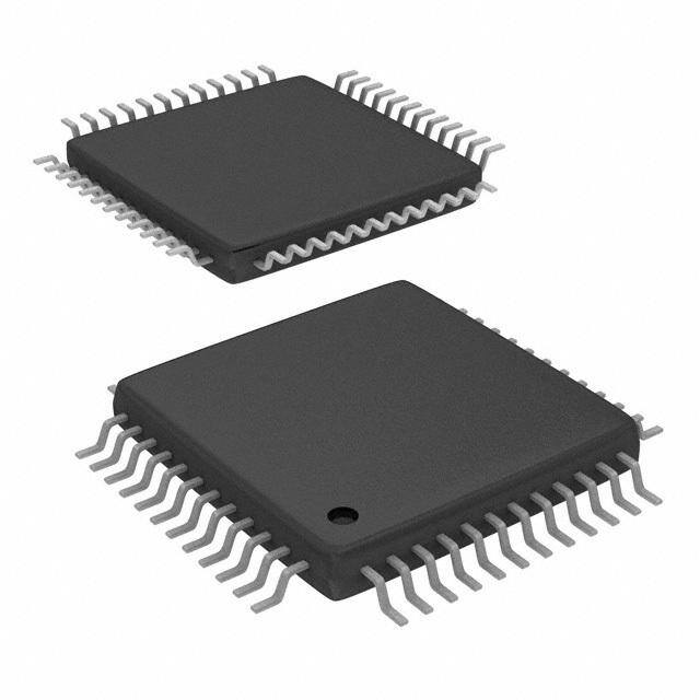
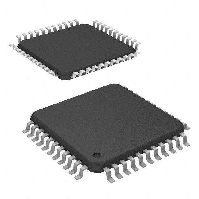
| 供应商器件封装 | 48-QFP(7x7) |
| 其它名称 | 336-1244 |
| 包装 | 托盘 |
| 单位重量 | 130.490 mg |
| 可用A/D通道 | 32 |
| 可编程输入/输出端数量 | 32 |
| 商标 | Silicon Labs |
| 处理器系列 | C8051 |
| 外设 | 欠压检测/复位,POR,WDT |
| 安装风格 | SMD/SMT |
| 定时器数量 | 3 Timer |
| 封装 | Tray |
| 封装/外壳 | 48-TQFP |
| 封装/箱体 | TQFP-48 |
| 工作温度 | -40°C ~ 85°C |
| 工作电源电压 | 2.7 V to 3.6 V |
| 工厂包装数量 | 250 |
| 振荡器类型 | 内部 |
| 接口类型 | SPI, UART |
| 数据RAM大小 | 1.25 kB |
| 数据ROM大小 | 128 B |
| 数据Rom类型 | Flash |
| 数据总线宽度 | 8 bit |
| 数据转换器 | - |
| 最大工作温度 | + 85 C |
| 最大时钟频率 | 25 MHz |
| 最小工作温度 | - 40 C |
| 标准包装 | 250 |
| 核心 | 8051 |
| 核心处理器 | 8051 |
| 核心尺寸 | 8-位 |
| 片上ADC | Yes |
| 电压-电源(Vcc/Vdd) | 2.7 V ~ 3.6 V |
| 电源电压-最大 | 3.6 V |
| 电源电压-最小 | 2.7 V |
| 程序存储器大小 | 8 kB |
| 程序存储器类型 | 闪存Flash |
| 程序存储容量 | 8KB(8K x 8) |
| 系列 | C8051F236 |
| 输入/输出端数量 | 32 I/O |
| 连接性 | SPI,UART/USART |
| 速度 | 25MHz |


- 商务部:美国ITC正式对集成电路等产品启动337调查
- 曝三星4nm工艺存在良率问题 高通将骁龙8 Gen1或转产台积电
- 太阳诱电将投资9.5亿元在常州建新厂生产MLCC 预计2023年完工
- 英特尔发布欧洲新工厂建设计划 深化IDM 2.0 战略
- 台积电先进制程称霸业界 有大客户加持明年业绩稳了
- 达到5530亿美元!SIA预计今年全球半导体销售额将创下新高
- 英特尔拟将自动驾驶子公司Mobileye上市 估值或超500亿美元
- 三星加码芯片和SET,合并消费电子和移动部门,撤换高东真等 CEO
- 三星电子宣布重大人事变动 还合并消费电子和移动部门
- 海关总署:前11个月进口集成电路产品价值2.52万亿元 增长14.8%


PDF Datasheet 数据手册内容提取
C8051F2xx 8K ISP FLASH MCU Family Analog Peripherals Memory - SAR ADC - 256 bytes internal data RAM • 12-bit resolution ('F206) - 1024 bytes XRAM (available on 'F206/226/236) • 8-bit resolution ('F220/1/6) - 8 kB Flash; In-system programmable in 512 byte • ±1/4 LSB INL (8-bit) and ±2 LSB INL (12-bit) • Up to 100 ksps sectors • Up to 32 channel input multiplexer; each port Digital Peripherals I/O pin can be an ADC input - Two Comparators - Four byte wide Port I/O; All are 5 V tolerant • 16 programmable hysteresis states - Hardware UART and SPI bus • Configurable to generate interrupts or reset - 3 general purpose 16-bit counter/timers - V monitor and brown-out detector DD - Dedicated watch-dog timer On-Chip JTAG Debug - Bi-directional reset - On-chip debug circuitry facilitates full speed, - System clock: internal programmable oscillator, non-intrusive in-system debug (No emulator external crystal, external RC, or external clock required) Supply Voltage 2.7 to 3.6 V - Provides breakpoints, single-stepping, watchpoints, - Typical operating current: 10 mA @ 25 MHz stack monitor - Multiple power saving sleep and shutdown modes - Inspect/modify memory and registers (48-Pin TQFP and 32-Pin LQFP Version - Superior performance to emulation systems using Available) ICE-chips, target pods, and sockets Temperature Range: –40 to +85 °C - Complete, low cost development kit High Speed - 8051 mC Core - Pipelined Instruction Architecture; Executes 70% of Instructions in 1 or 2 System Clocks - Up to 25MIPS Throughput with 25MHz Clock - Expanded Interrupt Handler ANALOG PERIPHERALS DIGITAL I/O 0 SPI Bus ort X SAR P U AM PGA ADC UART UX ort 1 M P Timer 0 al Digit ort 2 + + Timer 1 P - - 3 VOLTAGE Timer 2 ort COMPARATORS P HIGH-SPEED CONTROLLER CORE 8051 CPU CLOCK EMULATION JTAG (25MIPS) CIRCUIT CIRCUITRY 8K x 8 1280 x 8 SANITY 22 INTERRUPTS ISP FLASH SRAM CONTROL Rev. 1.6 3/05 Copyright © 2005 by Silicon Laboratories C8051F2xx
C8051F2xx NOTES: 2 Rev. 1.6
C8051F2xx Table of Contents 1. System Overview.................................................................................................... 11 1.1. CIP-51TM Microcontroller Core........................................................................ 15 1.1.1. Fully 8051 Compatible.............................................................................. 15 1.1.2. Improved Throughput............................................................................... 15 1.1.3. Additional Features.................................................................................. 16 1.2. On-Board Memory............................................................................................ 17 1.3. JTAG ............................................................................................................ 18 1.4. Digital/Analog Configurable I/O......................................................................... 19 1.5. Serial Ports....................................................................................................... 20 1.6. Analog to Digital Converter............................................................................... 20 1.7. Comparators..................................................................................................... 21 2. Absolute Maximum Ratings.................................................................................. 23 3. Global DC Electrical Characteristics.................................................................... 24 4. Pinout and Package Definitions............................................................................ 25 5. ADC (8-Bit, C8051F220/1/6 Only)........................................................................... 32 5.1. Analog Multiplexer and PGA............................................................................. 32 5.2. ADC Modes of Operation.................................................................................. 33 5.3. ADC Programmable Window Detector............................................................. 37 6. ADC (12-Bit, C8051F206 Only)............................................................................... 40 6.1. Analog Multiplexer and PGA............................................................................. 40 6.2. ADC Modes of Operation.................................................................................. 41 6.3. ADC Programmable Window Detector............................................................. 46 7. Voltage Reference (C8051F206/220/221/226)....................................................... 50 8. Comparators........................................................................................................... 52 9. CIP-51 Microcontroller........................................................................................... 58 9.1. Instruction Set................................................................................................... 60 9.1.1. Instruction and CPU Timing..................................................................... 60 9.1.2. MOVX Instruction and Program Memory................................................. 60 9.2. Memory Organization........................................................................................ 65 9.2.1. Program Memory...................................................................................... 65 9.2.2. Data Memory............................................................................................ 65 9.2.3. General Purpose Registers...................................................................... 66 9.2.4. Bit Addressable Locations........................................................................ 66 9.2.5. Stack ....................................................................................................... 67 9.3. Special Function Registers............................................................................... 68 9.3.1. Register Descriptions............................................................................... 71 9.4. Interrupt Handler............................................................................................... 74 9.4.1. MCU Interrupt Sources and Vectors........................................................ 74 9.4.2. External Interrupts.................................................................................... 74 9.4.3. Software Controlled Interrupts.................................................................. 74 9.4.4. Interrupt Priorities..................................................................................... 76 9.4.5. Interrupt Latency...................................................................................... 76 9.4.6. Interrupt Register Descriptions................................................................. 77 Rev. 1.6 3
C8051F2xx 9.5. Power Management Modes.............................................................................. 83 9.5.1. Idle Mode.................................................................................................. 83 9.5.2. Stop Mode................................................................................................ 83 10.Flash Memory......................................................................................................... 85 10.1.Programming The Flash Memory..................................................................... 85 10.2.Security Options............................................................................................... 86 11.On-Chip XRAM (C8051F206/226/236).................................................................... 90 12.Reset Sources......................................................................................................... 91 12.1.Power-on Reset................................................................................................ 92 12.2.Software Forced Reset..................................................................................... 92 12.3.Power-fail Reset............................................................................................... 92 12.4.External Reset.................................................................................................. 93 12.5.Missing Clock Detector Reset.......................................................................... 93 12.6.Comparator 0 Reset......................................................................................... 93 12.7.Watchdog Timer Reset..................................................................................... 93 12.7.1.Watchdog Usage...................................................................................... 93 13.Oscillator................................................................................................................. 97 13.1.External Crystal Example............................................................................... 100 13.2.External RC Example..................................................................................... 100 13.3.External Capacitor Example........................................................................... 100 14.Port Input/Output.................................................................................................. 101 14.1.Port I/O Initialization....................................................................................... 101 14.2.General Purpose Port I/O............................................................................... 105 15.Serial Peripheral Interface Bus........................................................................... 110 15.1.Signal Descriptions......................................................................................... 111 15.1.1.Master Out, Slave In.............................................................................. 111 15.1.2.Master In, Slave Out.............................................................................. 111 15.1.3.Serial Clock............................................................................................ 111 15.1.4.Slave Select........................................................................................... 111 15.2.Serial Clock Timing......................................................................................... 113 15.3.SPI Special Function Registers...................................................................... 113 16.UART...................................................................................................................... 117 16.1.UART Operational Modes.............................................................................. 118 16.1.1.Mode 0: Synchronous Mode.................................................................. 118 16.1.2.Mode 1: 8-Bit UART, Variable Baud Rate.............................................. 119 16.1.3.Mode 2: 9-Bit UART, Fixed Baud Rate.................................................. 121 16.1.4.Mode 3: 9-Bit UART, Variable Baud Rate.............................................. 121 16.2.Multiprocessor Communications.................................................................... 122 17.Timers.................................................................................................................... 125 17.1.Timer 0 and Timer 1....................................................................................... 125 17.1.1.Mode 0: 13-bit Counter/Timer................................................................ 125 17.1.2.Mode 1: 16-bit Counter/Timer................................................................ 126 17.1.3.Mode 2: 8-bit Counter/Timer with Auto-Reload...................................... 127 17.1.4.Mode 3: Two 8-bit Counter/Timers (Timer 0 Only)................................. 128 4 Rev. 1.6
C8051F2xx 17.2.Timer 2 .......................................................................................................... 133 17.2.1.Mode 0: 16-bit Counter/Timer with Capture........................................... 134 17.2.2.Mode 1: 16-bit Counter/Timer with Auto-Reload.................................... 135 17.2.3.Mode 2: Baud Rate Generator............................................................... 136 18.JTAG...................................................................................................................... 139 18.1.Flash Programming Commands..................................................................... 140 18.2.Boundary Scan Bypass and ID Code............................................................. 143 18.2.1.BYPASS Instruction............................................................................... 143 18.2.2.IDCODE Instruction................................................................................ 143 18.3.Debug Support............................................................................................... 143 Contact Information.................................................................................................. 144 Rev. 1.6 5
C8051F2xx NOTES: 6 Rev. 1.6
C8051F2xx List of Figures and Tables 1. System Overview Table 1.1. Product Selection Guide........................................................................ 11 Figure 1.1. C8051F206, C8051F220 and C8051F226 Block Diagram (48 TQFP).. 12 Figure 1.2. C8051F221 Block Diagram (32 LQFP).................................................. 13 Figure 1.3. C8051F230 and C8051F236 Block Diagram (48 TQFP)....................... 14 Figure 1.4. C8051F231 Block Diagram (32 LQFP).................................................. 15 Figure 1.5. Comparison of Peak MCU Throughputs................................................ 16 Figure 1.6. Comparison of Peak MCU Throughputs................................................ 17 Figure 1.7. On-Board Memory Map.......................................................................... 18 Figure 1.8. Degub Environment Diagram................................................................. 19 Figure 1.9. Port I/O Functional Block Diagram......................................................... 20 Figure 1.10. ADC Diagram....................................................................................... 21 Figure 1.11. Comparator Diagram............................................................................ 22 2. Absolute Maximum Ratings Table 2.1. Absolute Maximum Ratings*.................................................................. 23 3. Global DC Electrical Characteristics Table 3.1. Global DC Electrical Characteristics...................................................... 24 4. Pinout and Package Definitions Table 4.1. Pin Definitions........................................................................................ 25 Figure 4.1. TQFP-48 Pin Diagram............................................................................ 28 Figure 4.2. LQFP-32 Pin Diagram............................................................................ 29 Figure 4.3. TQFP-48 Package Drawing................................................................... 30 Figure 4.4. LQFP-32 Package Drawing................................................................... 31 5. ADC (8-Bit, C8051F220/1/6 Only) Figure 5.1. 8-Bit ADC Functional Block Diagram..................................................... 32 Figure 5.2. 12-Bit ADC Track and Conversion Example Timing.............................. 33 Figure 5.3. 8-Bit ADC Window Interrupt Examples.................................................. 38 Table 5.1. 8-Bit ADC Electrical Characteristics....................................................... 39 6. ADC (12-Bit, C8051F206 Only) Figure 6.1. 12-Bit ADC Functional Block Diagram................................................... 40 Figure 6.2. 12-Bit ADC Track and Conversion Example Timing.............................. 41 Figure 6.3. 12-Bit ADC Window Interrupt Examples, Right Justified Data............... 47 Figure 6.4. 12-Bit ADC Window Interrupt Examples, Left Justified Data................. 48 Table 6.1. 12-Bit ADC Electrical Characteristics (C8015F206 only)....................... 49 7. Voltage Reference (C8051F206/220/221/226) Figure 7.1. Voltage Reference Functional Block Diagram....................................... 50 Table 7.1. Reference Electrical Characteristics...................................................... 51 8. Comparators Figure 8.1. Comparator Functional Block Diagram.................................................. 53 Figure 8.2. Comparator Hysteresis Plot................................................................... 54 Table 8.1. Comparator Electrical Characteristics.................................................... 57 9. CIP-51 Microcontroller Figure 9.1. CIP-51 Block Diagram............................................................................ 58 Rev. 1.6 7
C8051F2xx Table 9.1. CIP-51 Instruction Set Summary............................................................ 60 Figure 9.2. Memory Map.......................................................................................... 66 Table 9.2. Special Function Register Memory Map................................................ 68 Table 9.3. Special Function Registers.................................................................... 69 Table 9.4. Interrupt Summary................................................................................. 75 10.Flash Memory Table 10.1. Flash Memory Electrical Characteristics............................................... 86 Figure 10.1. Flash Program Memory Security Bytes................................................ 87 11.On-Chip XRAM (C8051F206/226/236) 12.Reset Sources Figure 12.1. Reset Sources Diagram....................................................................... 91 Figure 12.2. VDD Monitor Timing Diagram.............................................................. 92 Table 12.1. VDD Monitor Electrical Characteristics.................................................. 96 13.Oscillator Figure 13.1. Oscillator Diagram................................................................................ 97 Table 13.1. Internal Oscillator Electrical Characteristics.......................................... 98 14.Port Input/Output Figure 14.1. Port I/O Functional Block Diagram..................................................... 102 Figure 14.2. Port I/O Cell Block Diagram............................................................... 102 Table 14.1. Port I/O DC Electrical Characteristics.................................................. 109 15.Serial Peripheral Interface Bus Figure 15.1. SPI Block Diagram............................................................................. 110 Figure 15.2. SPI Block Diagram............................................................................. 111 Figure 15.3. Full Duplex Operation......................................................................... 112 Figure 15.4. Full Duplex Operation......................................................................... 113 16.UART Figure 16.1. UART Block Diagram......................................................................... 117 Table 16.1. UART Modes....................................................................................... 118 Figure 16.2. UART Mode 0 Interconnect................................................................ 118 Figure 16.3. UART Mode 0 Timing Diagram.......................................................... 118 Figure 16.4. UART Mode 1 Timing Diagram.......................................................... 119 Figure 16.5. UART Modes 1, 2, and 3 Interconnect Diagram................................ 120 Figure 16.6. UART Modes 2 and 3 Timing Diagram.............................................. 121 Figure 16.7. UART Multi-Processor Mode Interconnect Diagram.......................... 122 Table 16.2. Oscillator Frequencies for Standard Baud Rates................................ 122 17.Timers Figure 17.1. T0 Mode 0 Block Diagram.................................................................. 126 Figure 17.2. T0 Mode 2 Block Diagram.................................................................. 127 Figure 17.3. T0 Mode 3 Block Diagram.................................................................. 128 Figure 17.4. T2 Mode 0 Block Diagram.................................................................. 134 Figure 17.5. T2 Mode 1 Block Diagram.................................................................. 135 Figure 17.6. T2 Mode 2 Block Diagram.................................................................. 136 18.JTAG 8 Rev. 1.6
C8051F2xx List of Registers SFR Definition 5.1. AMX0SL: AMUX Channel Select . . . . . . . . . . . . . . . . . . . . . . . . . . 34 SFR Definition 5.2. ADC0CF: ADC Configuration Register . . . . . . . . . . . . . . . . . . . . . 35 SFR Definition 5.3. ADC0CN: ADC Control (C8051F220/1/6 and C8051F206) . . . . . . 36 SFR Definition 5.4. ADC0H: ADC Data Word (‘F220/1/6 and ‘F206) . . . . . . . . . . . . . 37 SFR Definition 5.5. ADC0GTH: ADC Greater-Than Data (‘F220/1/6 and ‘F206) . . . . . 37 SFR Definition 5.6. ADC0LTH: ADC Less-Than Data Byte (‘F220/1/6 and ‘F206) . . . . 37 SFR Definition 6.1. AMX0SL: AMUX Channel Select . . . . . . . . . . . . . . . . . . . . . . . . . . 42 SFR Definition 6.2. ADC0CF: ADC Configuration (‘F220/1/6 and ‘F206) . . . . . . . . . . . 43 SFR Definition 6.3. ADC0CN: ADC Control (‘F220/1/6 and ‘F206) . . . . . . . . . . . . . . . 44 SFR Definition 6.4. ADC0H: ADC Data Word MSB (C8051F206) . . . . . . . . . . . . . . . . 45 SFR Definition 6.5. ADC0L: ADC Data Word LSB (C8051F206) . . . . . . . . . . . . . . . . 45 SFR Definition 6.6. ADC0GTH: ADC Greater-Than Data High Byte (C8051F206) . . . 46 SFR Definition 6.7. ADC0GTL: ADC Greater-Than Data Low Byte (C8051F206) . . . . 46 SFR Definition 6.8. ADC0LTH: ADC Less-Than Data High Byte (C8051F206) . . . . . . 46 SFR Definition 6.9. ADC0LTL: ADC Less-Than Data Low Byte (C8051F206) . . . . . . . 47 SFR Definition 7.1. REF0CN: Reference Control . . . . . . . . . . . . . . . . . . . . . . . . . . . . 50 SFR Definition 8.1. CPT0CN: Comparator 0 Control . . . . . . . . . . . . . . . . . . . . . . . . . . 55 SFR Definition 8.2. CPT1CN: Comparator 1 Control . . . . . . . . . . . . . . . . . . . . . . . . . . 56 SFR Definition 9.1. SP: Stack Pointer . . . . . . . . . . . . . . . . . . . . . . . . . . . . . . . . . . . . . . 71 SFR Definition 9.2. DPL: Data Pointer Low Byte . . . . . . . . . . . . . . . . . . . . . . . . . . . . . 71 SFR Definition 9.3. DPH: Data Pointer High Byte . . . . . . . . . . . . . . . . . . . . . . . . . . . . . 71 SFR Definition 9.4. PSW: Program Status Word . . . . . . . . . . . . . . . . . . . . . . . . . . . . . 72 SFR Definition 9.5. ACC: Accumulator . . . . . . . . . . . . . . . . . . . . . . . . . . . . . . . . . . . . . 73 SFR Definition 9.6. B: B Register . . . . . . . . . . . . . . . . . . . . . . . . . . . . . . . . . . . . . . . . . 73 SFR Definition 9.7. SWCINT: Software Controlled Interrupt Register . . . . . . . . . . . . . 75 SFR Definition 9.8. IE: Interrupt Enable . . . . . . . . . . . . . . . . . . . . . . . . . . . . . . . . . . . . 77 SFR Definition 9.9. IP: Interrupt Priority . . . . . . . . . . . . . . . . . . . . . . . . . . . . . . . . . . . . 78 SFR Definition 9.10. EIE1: Extended Interrupt Enable 1 . . . . . . . . . . . . . . . . . . . . . . . 79 SFR Definition 9.11. EIE2: Extended Interrupt Enable 2 . . . . . . . . . . . . . . . . . . . . . . . 80 SFR Definition 9.12. EIP1: Extended Interrupt Priority 1 . . . . . . . . . . . . . . . . . . . . . . . 81 SFR Definition 9.13. EIP2: Extended Interrupt Priority 2 . . . . . . . . . . . . . . . . . . . . . . . 82 SFR Definition 9.14. PCON: Power Control Register . . . . . . . . . . . . . . . . . . . . . . . . . . 84 SFR Definition 10.1. PSCTL: Program Store RW Control . . . . . . . . . . . . . . . . . . . . . . 88 SFR Definition 10.2. FLSCL: Flash Memory Timing Prescaler . . . . . . . . . . . . . . . . . . . 89 SFR Definition 10.3. FLACL: Flash Access Limit . . . . . . . . . . . . . . . . . . . . . . . . . . . . . 89 SFR Definition 11.1. EMI0CN: External Memory Interface Control . . . . . . . . . . . . . . . 90 SFR Definition 12.1. WDTCN: Watchdog Timer Control . . . . . . . . . . . . . . . . . . . . . . . 94 SFR Definition 12.2. RSTSRC: Reset Source . . . . . . . . . . . . . . . . . . . . . . . . . . . . . . . 95 SFR Definition 13.1. OSCICN: Internal Oscillator Control . . . . . . . . . . . . . . . . . . . . . . 98 SFR Definition 13.2. OSCXCN: External Oscillator Control . . . . . . . . . . . . . . . . . . . . . 99 SFR Definition 14.1. PRT0MX: Port I/O MUX Register 0 . . . . . . . . . . . . . . . . . . . . . . 103 SFR Definition 14.2. PRT1MX: Port I/O MUX Register 1 . . . . . . . . . . . . . . . . . . . . . . 104 SFR Definition 14.3. PRT2MX: Port I/O MUX Register 2 . . . . . . . . . . . . . . . . . . . . . . 104 Rev. 1.6 9
C8051F2xx SFR Definition 14.4. P0: Port0 Register . . . . . . . . . . . . . . . . . . . . . . . . . . . . . . . . . . . 105 SFR Definition 14.5. PRT0CF: Port0 Configuration Register . . . . . . . . . . . . . . . . . . . 105 SFR Definition 14.6. P0MODE: Port0 Digital/Analog Input Mode . . . . . . . . . . . . . . . . 106 SFR Definition 14.7. P1: Port1 Register . . . . . . . . . . . . . . . . . . . . . . . . . . . . . . . . . . . 106 SFR Definition 14.8. PRT1CF: Port1 Configuration Register . . . . . . . . . . . . . . . . . . . 106 SFR Definition 14.9. P1MODE: Port1 Digital/Analog Input Mode . . . . . . . . . . . . . . . . 107 SFR Definition 14.10. P2: Port2 Register . . . . . . . . . . . . . . . . . . . . . . . . . . . . . . . . . . 107 SFR Definition 14.11. PRT2CF: Port2 Configuration Register . . . . . . . . . . . . . . . . . . 107 SFR Definition 14.12. P2MODE: Port2 Digital/Analog Input Mode . . . . . . . . . . . . . . . 108 SFR Definition 14.13. P3: Port3 Register* . . . . . . . . . . . . . . . . . . . . . . . . . . . . . . . . . 108 SFR Definition 14.14. PRT3CF: Port3 Configuration Register* . . . . . . . . . . . . . . . . . 108 SFR Definition 14.15. P3MODE: Port3 Digital/Analog Input Mode* . . . . . . . . . . . . . . 109 SFR Definition 15.1. SPI0CFG: SPI Configuration . . . . . . . . . . . . . . . . . . . . . . . . . . . 114 SFR Definition 15.2. SPI0CN: SPI Control . . . . . . . . . . . . . . . . . . . . . . . . . . . . . . . . . 115 SFR Definition 15.3. SPI0CKR: SPI Clock Rate Register . . . . . . . . . . . . . . . . . . . . . . 116 SFR Definition 15.4. SPI0DAT: SPI Data Register . . . . . . . . . . . . . . . . . . . . . . . . . . . 116 SFR Definition 16.1. SBUF: Serial (UART) Data Buffer . . . . . . . . . . . . . . . . . . . . . . . 123 SFR Definition 16.2. SCON: Serial Port Control . . . . . . . . . . . . . . . . . . . . . . . . . . . . . 124 SFR Definition 17.1. TCON: Timer Control . . . . . . . . . . . . . . . . . . . . . . . . . . . . . . . . . 129 SFR Definition 17.2. TMOD: Timer Mode . . . . . . . . . . . . . . . . . . . . . . . . . . . . . . . . . . 130 SFR Definition 17.3. CKCON: Clock Control . . . . . . . . . . . . . . . . . . . . . . . . . . . . . . . 131 SFR Definition 17.4. TL0: Timer 0 Low Byte . . . . . . . . . . . . . . . . . . . . . . . . . . . . . . . . 132 SFR Definition 17.5. TL1: Timer 1 Low Byte . . . . . . . . . . . . . . . . . . . . . . . . . . . . . . . . 132 SFR Definition 17.6. TH0: Timer 0 High Byte . . . . . . . . . . . . . . . . . . . . . . . . . . . . . . . 132 SFR Definition 17.7. TH1: Timer 1 High Byte . . . . . . . . . . . . . . . . . . . . . . . . . . . . . . . 132 SFR Definition 17.8. T2CON: Timer 2 Control . . . . . . . . . . . . . . . . . . . . . . . . . . . . . . 137 SFR Definition 17.9. RCAP2L: Timer 2 Capture Register Low Byte . . . . . . . . . . . . . . 138 SFR Definition 17.10. RCAP2H: Timer 2 Capture Register High Byte . . . . . . . . . . . . 138 SFR Definition 17.11. TL2: Timer 2 Low Byte . . . . . . . . . . . . . . . . . . . . . . . . . . . . . . . 138 SFR Definition 17.12. TH2: Timer 2 High Byte . . . . . . . . . . . . . . . . . . . . . . . . . . . . . . 138 JTAG Register Definition 18.1. IR: JTAG Instruction . . . . . . . . . . . . . . . . . . . . . . . . . 139 JTAG Register Definition 18.2. FLASHCON: JTAG Flash Control . . . . . . . . . . . . . . . 141 JTAG Register Definition 18.3. FLASHADR: JTAG Flash Address . . . . . . . . . . . . . . 141 JTAG Register Definition 18.4. FLASHDAT: JTAG Flash Data . . . . . . . . . . . . . . . . . 142 JTAG Register Definition 18.5. FLASHSCL: JTAG Flash Scale . . . . . . . . . . . . . . . . . 142 JTAG Register Definition 18.6. DEVICEID: JTAG Device ID . . . . . . . . . . . . . . . . . . . 143 10 Rev. 1.6
C8051F2xx 1. System Overview The C8051F2xx is a family of fully integrated, mixed-signal System on a Chip MCU's available with a true 12-bit ('F206) multi-channel ADC, 8-bit multi-channel ADC ('F220/1/6 and 'F206), or without an ADC ('F230/1/6). Each model features an 8051-compatible microcontroller core with 8 kB of Flash memory. There are also UART and SPI serial interfaces implemented in hardware (not "bit-banged" in user soft- ware). Products in this family feature 22 or 32 general purpose I/O pins, some of which can be used for assigned digital peripheral interface. Any pins may be configured for use as analog input to the analog-to- digital converter ('F220/1/6 and 'F206 only). (See the Product Selection Guide in Table 1.1 for a quick ref- erence of each MCUs' feature set.) Other features include an on-board V monitor, WDT, and clock oscillator. On-board Flash memory can DD be reprogrammed in-circuit, and may also be used for non-volatile data storage. Integrated peripherals can also individually shut down any or all of the peripherals to conserve power. All parts have 256 bytes of SRAM. Also, an additional 1024 bytes of RAM is available in the 'F206/226/236. On-board JTAG debug support allows non-intrusive (uses no on-chip resources), full speed, in-circuit debug using the production MCU installed in the final application. This debug system supports inspection and modification of memory and registers, setting breakpoints, watchpoints, single stepping, run and halt commands. All analog and digital peripherals are fully functional when emulating using JTAG. Each MCU is specified for 2.7 to 3.6 V operation over the industrial temperature range (–45 to +85 °C) and is available in the 48-pin TFQP and 32-pin LFQP. The Port I/Os are tolerant for input signals up to 5 V. Table 1.1. Product Selection Guide ) s MIPS (Peak) Flash Memory RAM SPI UART Timers (16-bit) Digital Port I/O’s ADC Resolution (bits) ADC Max Speed (ksp ADC Inputs Voltage Comparators Package C8051F206 25 8 k 1280 3 32 12 100 32 2 48TQFP C8051F220 25 8 k 256 3 32 8 100 32 2 48TQFP C8051F221 25 8 k 256 3 22 8 100 22 2 32LQFP C8051F226 25 8 k 1280 3 32 8 100 32 2 48TQFP C8051F230 25 8 k 256 3 32 — — — 2 48TQFP C8051F231 25 8 k 256 3 22 — — — 2 32LQFP C8051F236 25 8 k 1280 3 32 — — — 2 48TQFP Rev. 1.6 11
C8051F2xx Port I/O Mode & Config. VDD Digital Power VDD Port 0 P P0.0/TX GND ULaAtRchT P0 0 PPP000...123///R//XIINNTT01 GND D P0.4/T0 Timer 0 M r P0.5/T1 Timer 1 UX v PP00..67//TT22EX Timer 2 1024 Byte XRAM Port 1 TTTTCMDDKSIO JLToAgiGc Emulation HW 80 ('FA2v0a6ila/Fb2le2 6in) Latch CP0+ P1 P1 PPPP1111....0123////CCCCPPPP0001+-+ /RST Reset 51 F8LkAbyStHe CP0 CP0 CCPP01-+ MU Dvr PPPP1111....4567///CCSPPY11S-CLK VDD CP1 CP1 CP1- X VDDMONEN Monitor, 256 byte WDT C SRAM VREF Comparator P P2.0/SCK XXTTAALL12 OECsxcitreicllruanitatolr System Clock or SFR Bus PCoortn 2fig. P2 D2 PPPP2222....1234///MMNIOSSSSOI OInstceilrlnaatolr e LSaPtcIh MU vr PPP222...567 Port Mux X P P3.0 Control 3 PP33..12 NC Clock & Reset Port 3 P3.3 NNCC Configuration Latch Dr PP33..45 ADC VDD VREF v PP33..67 Config. & Control A VREF SAR M AIN0-AIN31 ADC U X Figure 1.1. C8051F206, C8051F220 and C8051F226 Block Diagram (48 TQFP) 12 Rev. 1.6
C8051F2xx Port I/O Mode & Config. Digital Power VDD Port 0 P P0.0/TX GND ULaAtRchT P0 0 PPP000...123///R//XIINNTT01 D P0.4/T0 Timer 0 M r P0.5/T1 Timer 1 UX v PP00..67//TT22EX Timer 2 Port 1 TCK 8 Latch P P1.0/CP0+ TTTMDDSIO JLToAgiGc Emulation HW 0 F8LkAbyStHe CP0+ P1 1 PPP111...123///CCCPPP001-+ /RST Reset 51 256 byte CP0 CP0 CCPP01-+ MU Dvr PPPP1111....4567///CCSPPY11S-CLK VDD SRAM CP1 CP1 CP1- X Monitor, WDT C VREF Comparator P P2.0/SCK XXTTAALL12 OECsxcitreicllrauntiatolr System Clock or SFR Bus PCoortn 2fig. P2 D2 PPPP2222....1234///MMNIOSSSSOI OInstceilrlnaatolr e LSaPtcIh MU vr P2.5 Port Mux X Control Clock & Reset Port 3 Configuration Latch ADC VDD VREF Config. & Control VREF A SAR M AIN0-AIN21 ADC U X Figure 1.2. C8051F221 Block Diagram (32 LQFP) Rev. 1.6 13
C8051F2xx Port I/O Mode & Config. Digital Power VDD Port 0 P P0.0/TX GGNNDD ULaAtRchT P0 D0 PPPP0000....1234////R//TXII0NNTT01 Timer 0 M r P0.5/T1 Timer 1 UX v PP00..67//TT22EX Timer 2 1024 Byte Port 1 TCK 8 XRAM Latch P P1.0/CP0+ TTTMDDSIO JLToAgiGc Emulation HW 0 (Av'aFi2la3b6l)e in CP0+ P1 1 PPP111...123///CCCPPP001-+ /RST Reset 51 F8LkAbyStHe CP0 CP0 CCPP01-+ MU Dvr PPPP1111....4567///CCSPPY11S-CLK VDD CP1 CP1 CP1- X MONEN Monitor, 256 byte WDT C SRAM Comparator P P2.0/SCK XXTTAALL12 OECsxcitreicllraunitatolr System Clock or SFR Bus PCoortn 2fig. P2 D2 PPPP2222....1234///MMNIOSSSSOI NC OInstceilrlnaatolr e LSaPtcIh MU vr PPP222...567 NNNCCC PCoortn Mtroulx X P3 PPP333...012 NC CCloonckfi g&u rRaetisoent PLoartct h3 Dr PPP333...345 v PP33..67 Figure 1.3. C8051F230 and C8051F236 Block Diagram (48 TQFP) 14 Rev. 1.6
C8051F2xx Port I/O Mode & Config. Digital Power VDD Port 0 P P0.0/TX GND ULaAtRchT P0 0 PPP000...123///R//XIINNTT01 D P0.4/T0 Timer 0 M r P0.5/T1 Timer 1 UX v PP00..67//TT22EX Timer 2 Port 1 TCK 8 Latch P P1.0/CP0+ TTTMDDSIO JLToAgiGc Emulation HW 0 F8LkAbyStHe CP0+ P1 1 PPP111...123///CCCPPP001-+ /RST Reset 51 256 byte CP0 CP0 CCPP01-+ MU Dvr PPPP1111....4567///CCSPPY11S-CLK VDD SRAM CP1 CP1 CP1- X Monitor, WDT C Comparator P P2.0/SCK XXTTAALL12 OECsxcitreicllrauntiatolr System Clock or SFR Bus PCoortn 2fig. P2 D2 PPPP2222....1234///MMNIOSSSSOI OInstceilrlnaatolr e LSaPtcIh MU vr P2.5 Port Mux X Control Clock & Reset Port 3 Configuration Latch NC Figure 1.4. C8051F231 Block Diagram (32 LQFP) 1.1. CIP-51TM Microcontroller Core 1.1.1. Fully 8051 Compatible The C8051F206, C8051F220/1/6 and C8051F230/1/6 utilize Silcon Labs’ proprietary CIP-51 microcontrol- ler core. The CIP-51 is fully compatible with the MCS-51TM instruction set. Standard 803x/805x assem- blers and compilers can be used to develop software. The core contains the peripherals included with a standard 8052, including three 16-bit counter/timers, a full-duplex UART, 256 bytes of internal RAM, an optional 1024 bytes of XRAM, 128 byte Special Function Register (SFR) address space, and four byte- wide I/O Ports. 1.1.2. Improved Throughput The CIP-51 employs a pipelined architecture that greatly increases its instruction throughput over the stan- dard 8051 architecture. In a standard 8051, all instructions except for MUL and DIV take 12 or 24 system clock cycles to execute with a maximum system clock of 12 MHz. By contrast, the CIP-51 core executes 70% of its instructions in one or two system clock cycles, with only four instructions taking more than four system clock cycles. The CIP-51 has a total of 109 instructions. The number of instructions versus the system clock cycles to execute them is as follows: Instructions 26 50 5 14 7 3 1 2 1 Clocks to Execute 1 2 2/3 3 3/4 4 4/5 5 8 Rev. 1.6 15
C8051F2xx With the CIP-51's maximum system clock at 25 MHz, it has a peak throughput of 25 MIPS. Figure 1.5 shows a comparison of peak throughputs of various 8-bit microcontroller cores with their maximum system clocks. 25 20 S P I 15 M 10 5 Silicon Labs Microchip Philips ADuC812 CIP-51 PIC17C75x 80C51 8051 (25 MHz clk) (33 MHz clk) (33 MHz clk) (16 MHz clk) Figure 1.5. Comparison of Peak MCU Throughputs 1.1.3. Additional Features The C8051F206, C8051F220/1/6 and C8051F230/1/6 have several key enhancements both inside and outside the CIP-51 core to improve overall performance and ease of use in end applications. The extended interrupt handler provides 22 interrupt sources into the CIP-51 (as opposed to 7 for the stan- dard 8051), allowing the numerous analog and digital peripherals to interrupt the controller. (An interrupt driven system requires less intervention by the MCU, giving it more effective throughput.) The extra inter- rupt sources are very useful when building multi-tasking, real-time systems. There are up to six reset sources for the MCU: an on-board V monitor, a Watchdog Timer, a missing DD clock detector, a voltage level detection from Comparator 0, a forced software reset, and an external reset pin. The RST pin is bi-directional, accommodating an external reset, or allowing the internally generated reset to be output on the RST pin. The on-board V monitor is enabled by pulling the MONEN pin high DD (digital 1). The user may disable each reset source except for the V monitor and Reset Input Pin from DD software. The watchdog timer may be permanently enabled in software after a power-on reset during MCU initialization. The MCU has an internal, stand-alone clock generator that is used by default as the system clock after reset. If desired, the clock source may be switched "on the fly" to the external oscillator, which can use a crystal, ceramic resonator, capacitor, RC, or external clock source to generate the system clock. This can be extremely useful in low power applications, allowing the MCU to run from a slow (power saving) exter- nal crystal source, while periodically switching to the fast (up to 16MHz) internal oscillator as needed. 16 Rev. 1.6
C8051F2xx VDD MonEn Supply Monitor Supply + Reset /RST - Timeout (wired-OR) Comparator 0 CP0+ + - CP0- C0RSEF Missing Reset System Clock Funnel Clock Detector WDT EN CDable Mn E EN PRE SWRSF WDTEnable WDTStrobe CIP-(S5o1ftwareS yRsetesmet )Reset Core Figure 1.6. Comparison of Peak MCU Throughputs 1.2. On-Board Memory The CIP-51 has a standard 8051 program and data address configuration. It includes 256 bytes of data RAM, with the upper 128 bytes dual-mapped. An optional 1024 bytes of XRAM is available on the 'F206, 'F226 and 'F236. Indirect addressing accesses the upper 128 bytes of general purpose RAM, and direct addressing accesses the 128-byte SFR address space. The lower 128 bytes of RAM are accessible via direct or indirect addressing. The first 32 bytes are addressable as four banks of general purpose regis- ters, and the next 16 bytes can be byte addressable or bit addressable. The MCU's program memory consists of 8 k + 128 bytes of Flash. This memory may be reprogrammed in- system in 512 byte sectors, and requires no special off-chip programming voltage. The 512 bytes from addresses 0x1E00 to 0x1FFF are reserved for factory use. There is also a user programmable 128-byte sector at address 0x2000 to 0x207F, which may be useful as a table for storing software constants, nonvol- atile configuration information, or as additional program space. See Figure 1.7 for the MCU system mem- ory map. Rev. 1.6 17
C8051F2xx PROGRAM MEMORY DATA MEMORY 0x207F 0xFF Upper 128 RAM Special Function 128 Byte ISP FLASH 0x2000 (Indirect Addressing Register's 0x1FFF 0x80 Only) (Direct Addressing Only) RESERVED 0x1E00 0x7F 0x1DFF (Direct and Indirect Addressing) Lower 128 RAM 0x30 (Direct and Indirect FLASH 0x2F Addressing) Bit Addressable 0x20 (In-System 0x1F General Purpose Programmable in 512 0x00 Registers Byte Sectors) 0x3FF 0x0000 Mapped into 1024 Byte External Data Memory XRAM Space (C8051F226/236/206 only) 0x000 Figure 1.7. On-Board Memory Map 1.3. JTAG The C8051F2xx have on-chip JTAG and debug logic that provide non-intrusive, full speed, in-circuit debug using the production part installed in the end application using the four-pin JTAG I/F. The C8051F2xxDK is a development kit with all the hardware and software necessary to develop application code and perform in-circuit debug with the C8051F2xx. The kit includes software with a developer's studio and debugger, an integrated 8051 assembler, and an RS-232 to JTAG interface module referred to as the EC. It also has a target application board with a C8051F2xx installed and large prototyping area, plus the RS-232 and JTAG cables, and wall-mount power supply. The Development Kit requires a Windows OS (Windows 95 or later) computer with one available RS-232 serial port. As shown in Figure 1.8, the PC is connected via RS-232 to the EC. A six-inch ribbon cable connects the EC to the user's application board, picking up the four JTAG pins and V and GND. The EC takes its power from the application board. It requires roughly DD 20 mA at 2.7–3.6 V. For applications where there is not sufficient power available from the target board, the provided power supply can be connected directly to the EC. This is a vastly superior configuration for developing and debugging embedded applications compared to standard MCU Emulators, which use on-board "ICE Chips" and target cables and require the MCU in the application board to be socketed. Silicon Labs' debug environment both increases ease of use, and pre- serves the performance of the precision analog peripherals. 18 Rev. 1.6
C8051F2xx Silicon Labs Integrated Development Environment WINDOWS OS RS-232 SERIAL ADAPTER JTAG (x4), VDD, GND TARGET PCB VDD GND C8051 F2XX Figure 1.8. Degub Environment Diagram 1.4. Digital/Analog Configurable I/O The standard 8051 Ports (0, 1, 2, and 3) are available on the device. The ports behave like standard 8051 ports with a few enhancements. Each port pin can be configured as either a push-pull or open-drain output. Any input that is configured as an analog input will have its corresponding weak pull-up turned off. Digital resources (timers, SPI, UART, system clock, and comparators) are routed to corresponding I/O pins by configuring the port multiplexer. Port multiplexers are programmed by setting bits in SFR's (please see Section 14). Any of the 32 external port pins may be configured as either analog inputs or digital I/O (See Figure 1.9), so effectively, all port pins are dual function. Rev. 1.6 19
C8051F2xx PRTnMX PRTnCF & Registers PnMODE registers External T0,T1,T2 pins Timers P0.0/TX Port P0.1/RX UART 0 P0.2/INT0 P0.3/INT1 MUX Port0 I/O Cell P0.4/T0 External P0.5/T1 INT0 & INT1 P0.6/T2 P0.7/T2EX P1.0/CP0+ Comparators P1.1/CP0- 0 & 1 Port P1.2/CP0 1 P1.3/CP1+ MUX Port1 I/O Cell P1.4/CP1- P1.5/CP1 SYSCLK P1.6/SYSCLK P1.7 Any port pin may be configured via software as an analog input to the ADC P2.0/SCK P2.1/MISO Port P2.2/MOSI SPI 2 P2.3/NSS Port2 I/O Cell P2.4 MUX P2.5 P2.6 P2.7 P3.0 P3.1 P3.2 Port3 I/O Cell P3.3 A P3.4 ADC M P3.5 U P3.6 X P3.7 Figure 1.9. Port I/O Functional Block Diagram 1.5. Serial Ports The C8051F206, C8051F220/1/6 and C8051F230/1/6 include a Full-Duplex UART and SPI Bus. Each of the serial buses is fully implemented in hardware and makes extensive use of the CIP-51's interrupts, thus requiring very little intervention by the CPU. The serial buses do not have to "share" resources such as timers, interrupts, or Port I/O, so both of the serial buses may be used simultaneously. (You may use Tim- er1, Timer 2, or SYSCLK to generate baud rates for UART). 1.6. Analog to Digital Converter The C8051F220/1/6 has an on-chip 8-bit SAR ADC and the C8051F206 has a 12-bit SAR ADC with a pro- grammable gain amplifier. With a maximum throughput of 100ksps, the ADC offers true 8-bit with an INL of ±1/4 LSB, and or 12-bit accuracy with ±2 LSB. The voltage reference can be the power supply (V ), or DD an external reference voltage (VREF). Also, the system controller can place the ADC into a power-saving shutdown mode when not in use. A programmable gain amplifier follows the analog multiplexer. The gain can be set in software from 0.5 to 16 in powers of 2. Conversions can be initiated in two ways; a software command or an overflow on Timer 2. This flexibility allows the start of conversion to be triggered by software events, or convert continuously. A completed conversion causes an interrupt, or a status bit can be polled in software to determine the end of conver- sion. The resulting 8-bit data word is latched into an SFR upon completion of a conversion. 20 Rev. 1.6
C8051F2xx ADC data is continuously monitored by a programmable window detector, which interrupts the CPU when data is within the user-programmed window. This allows the ADC to monitor key system voltages in back- ground mode, without the use of CPU resources. VREF VDD AIN0 AIN1 Programmable Gain Amp AIN0-31 are port 0-3 pins -- any external . 100ksps 32-to-1 port pin may be configured as . an analog input AMUX + SAR . X (only 22 input port pins on - 'F221) ADC AIN31 GND Control & Data SFR Bus SFR's Figure 1.10. ADC Diagram 1.7. Comparators The MCU's have two on-chip voltage comparators. The inputs of the comparators are available at pack- age pins as illustrated in Figure 1.11. Each comparator's hysteresis is software programmable via special function registers (SFR's). Both voltage level and positive/negative going symmetry can be easily pro- grammed by the user. Additionally, comparator interrupts can be implemented on either rising or falling- edge output transitions. Please see 8.‘Comparators” on page 52 for details. Rev. 1.6 21
C8051F2xx CP0 P1.2 Port1 CP1 MUX P1.5 P1.0 + CP0 P1.1 - P1.3 CP0 + CP1 P1.4 - CP1 SFR's CIP-51 (Data and and Interrupt Cntrl) Handler Figure 1.11. Comparator Diagram 22 Rev. 1.6
C8051F2xx 2. Absolute Maximum Ratings Table 2.1. Absolute Maximum Ratings* Parameter Conditions Min Typ Max Units Ambient Temperature under Bias –55 — 125 °C Storage Temperature –65 — 150 °C Voltage on any Pin (except V and Port I/O) with –0.3 — V + V DD DD respect to DGND 0.3 Voltage on any Port I/O Pin or RST pins with respect to –0.3 — 5.8 V DGND Voltage on V with respect to DGND –0.3 4.2 V DD Total Power Dissipation — 1.0 800 W Maximum Output Current Sunk by any Port pin — — 200 mA Maximum Output Current Sunk by any other I/O pin — — 25 mA Maximum Output Current Sourced by any Port pin — — 200 mA Maximum Output Current Sourced by any other I/O pin — — 25 mA *Note: Stresses above those listed under “Absolute Maximum Ratings” may cause permanent damage to the device. This is a stress rating only and functional operation of the devices at those or any other conditions above those indicated in the operation listings of this specification is not implied. Exposure to maximum rating conditions for extended periods may affect device reliability. Rev. 1.6 23
C8051F2xx 3. Global DC Electrical Characteristics Table 3.1. Global DC Electrical Characteristics –40 to +85 °C unless otherwise specified. Parameter Conditions Min Typ Max Units Analog Supply Voltage1 2.7 3.0 3.6 V V supply current with ADC and Clock = 25 MHz — 13 — mA DD comparators active, and CPU Clock = 1 MHz 1.5 mA active Clock = 32 kHz 300 µA V supply current with ADC and Clock = 25 MHz — 9 — mA DD comparators active, and CPU inac- Clock = 1 MHz 1.8 mA tive (Idle Mode) Clock = 32 kHz 275 µA V supply current with ADC and Clock = 25 MHz — 12.5 — mA DD comparators inactive, and CPU Clock = 1 MHz 1.0 mA active Clock = 32 kHz 25 µA Digital Supply Current with CPU Clock = 25 MHz — 8.5 — mA inactive (Idle Mode) Clock = 1 MHz 1.4 mA Clock = 32 kHz 25 µA Digital Supply Current (Stop Mode), Oscillator not running — 10 — µA V monitor enabled DD Digital Supply Current (Stop Mode), Oscillator not running — 0.1 — µA V monitor disabled DD Digital Supply RAM Data Retention — 1.5 — V Voltage Specified Operating Temperature –40 — +85 °C Range SYSCLK (system clock — 0 25 MHz frequency)2 Tsysl (SYSCLK low time) 18 — — ns Tsysh (SYSCLK high time) 18 — — ns Notes: 1. Analog Supply AV+ must be greater than 1 V for V monitor to operate. DD 2. SYSCLK must be at least 32 kHz to enable debugging. 24 Rev. 1.6
C8051F2xx 4. Pinout and Package Definitions Table 4.1. Pin Definitions ‘F206, F220, ‘F221, 226, Name 230, 231 Type Description 236 48-Pin 32-Pin V 11,31 8 Digital Voltage Supply. DD GND 5,6,8, 9 Ground. (Note: Pins 5,6, and 8 on the 48-pin package are not 13,32 connected (NC), but it is recommended that they be connected to ground.) MONEN 12 D In Monitor Enable (on 48 pin package ONLY). Enables reset volt- age monitor function when pulled high (logic “1”). TCK 25 17 D In JTAG Test Clock with internal pull-up. TMS 26 18 D In JTAG Test-Mode Select with internal pull-up. TDI 28 20 D In JTAG Test Data Input with internal pull-up. TDI is latched on a rising edge of TCK. TDO 27 19 D Out JTAG Test Data Output. Data is shifted out on TDO on the falling edge of TCK. TDO output is a tri-state driver. XTAL1 9 6 A In Crystal Input. This pin is the return for the internal oscillator cir- cuit for a crystal or ceramic resonator. For a precision internal clock, connect a crystal or ceramic resonator from XTAL1 to XTAL2. If overdriven by an external CMOS clock, this becomes the system clock. XTAL2 10 7 A Out Crystal Output. This pin is the excitation driver for a crystal or ceramic resonator. RST 14 10 D I/O Chip Reset. Open-drain output of internal Voltage Supply moni- tor. Is driven low when V is < 2.7V and MONEN=1, or when a DD ‘1’is written to PORSF. An external source can force a system reset by driving this pin low. VREF 7 5 A I/O Voltage Reference. When configured as an input, this pin is the voltage reference for the ADC. Otherwise, V will be the refer- DD ence. NOTE: this pin is Not Connected (NC) on ‘F230/1/6. CP0+ 4 4 A In Comparator 0 Non-Inverting Input. CP0- 3 3 A In Comparator 0 Inverting Input. CP0 2 2 D Out Comparator 0 Output CP1+ 1 1 A In Comparator 1 Non-Inverting Input. CP1- 48 32 A In Comparator 1 Inverting Input. CP1 47 31 D Out Comparator 1 Output P0.0/TX 40 28 D I/O Port0 Bit0. (See the Port I/O Sub-System section for complete A In description). P0.1/RX 39 27 D I/O Port0 Bit1. (See the Port I/O Sub-System section for complete A In description). P0.2/INT0 38 26 D I/O Port0 Bit2. (See the Port I/O Sub-System section for complete A In description). Rev. 1.6 25
C8051F2xx Table 4.1. Pin Definitions (Continued) ‘F206, F220, ‘F221, 226, Name 230, 231 Type Description 236 48-Pin 32-Pin P0.3/INT1 37 25 D I/O Port0 Bit3. (See the Port I/O Sub-System section for complete A In description). P0.4/T0 36 24 D I/O Port0 Bit4. (See the Port I/O Sub-System section for complete A In description). P0.5/T1 35 23 D I/O Port0 Bit5. (See the Port I/O Sub-System section for complete A In description). P0.6/T2 34 22 D I/O Port0 Bit6. (See the Port I/O Sub-System section for complete A In description). P0.7/T2EX 33 21 D I/O Port0 Bit7. (See the Port I/O Sub-System section for complete A In description). P1.0/CP0+ 4 4 D I/O Port1 Bit0. (See the Port I/O Sub-System section for complete A In description). P1.1/CP0- 3 3 D I/O Port1 Bit1. (See the Port I/O Sub-System section for complete A In description). P1.2/CP0 2 2 D I/O Port1 Bit2. (See the Port I/O Sub-System section for complete A In description). P1.3/CP1+ 1 1 D I/O Port1 Bit3. (See the Port I/O Sub-System section for complete A In description). P1.4/CP1- 48 32 D I/O Port1 Bit4. (See the Port I/O Sub-System section for complete A In description). P1.5/CP1 47 31 D I/O Port1 Bit5. (See the Port I/O Sub-System section for complete A In description). P1.6/SYSCLK 46 30 D I/O Port1 Bit6. (See the Port I/O Sub-System section for complete A In description). P1.7 45 29 D I/O Port1 Bit7. (See the Port I/O Sub-System section for complete A In description). P2.0/SCK 24 16 D I/O Port2 Bit0. (See the Port I/O Sub-System section for complete A In description). P2.1/MISO 23 15 D I/O Port2 Bit1. (See the Port I/O Sub-System section for complete A In description). P2.2/MOSI 22 14 D I/O Port2 Bit2. (See the Port I/O Sub-System section for complete A In description). P2.3/NSS 21 13 D I/O Port2 Bit3. (See the Port I/O Sub-System section for complete A In description). P2.4 15 11 D I/O Port2 Bit4. (See the Port I/O Sub-System section for complete A In description). P2.5 16 12 D I/O Port2 Bit5. (See the Port I/O Sub-System section for complete A In description). P2.6 17 D I/O Port2 Bit6. (See the Port I/O Sub-System section for complete A In description). 26 Rev. 1.6
C8051F2xx Table 4.1. Pin Definitions (Continued) ‘F206, F220, ‘F221, 226, Name 230, 231 Type Description 236 48-Pin 32-Pin P2.7 18 D I/O Port2 Bit7. (See the Port I/O Sub-System section for complete A In description). P3.0 44 D I/O Port3 Bit0. (See the Port I/O Sub-System section for complete A In description). P3.1 43 D I/O Port3 Bit1. (See the Port I/O Sub-System section for complete A In description). P3.2 42 D I/O Port3 Bit2. (See the Port I/O Sub-System section for complete A In description). P3.3 41 D I/O Port3 Bit3. (See the Port I/O Sub-System section for complete A In description). P3.4 30 D I/O Port3 Bit4. (See the Port I/O Sub-System section for complete A In description). P3.5 29 D I/O Port3 Bit5. (See the Port I/O Sub-System section for complete A In description). P3.6 20 D I/O Port3 Bit6. (See the Port I/O Sub-System section for complete A In description). P3.7 19 D I/O Port3 Bit7. (See the Port I/O Sub-System section for complete A In description). Rev. 1.6 27
C8051F2xx K L 4/CP1- 5/CP1 6/SYSC 7 0 1 2 3 0/TX 1/RX 2/INT0 3/INT1 1. 1. 1. 1. 3. 3. 3. 3. 0. 0. 0. 0. P P P P P P P P P P P P 8 7 6 5 4 3 2 1 0 9 8 7 4 4 4 4 4 4 4 4 4 3 3 3 P1.3/CP1+ 1 36 P0.4/T0 P1.2/CP0 2 35 P0.5/T1 P1.1/CP0- 3 34 P0.6/T2 P1.0/CP0+ 4 33 P0.7/T2EX NC 5 C8051F220/6 32 GND NC 6 C8051F230/6 31 VDD VREF* 7 30 P3.4 C8051F206 NC 8 29 P3.5 XTAL1 9 28 TDI XTAL2 10 27 TDO VDD 11 26 TMS MONEN 12 *Pin 7 is a No Connect on 25 TCK 'F230/6 3 4 5 6 7 8 9 0 1 2 3 4 1 1 1 1 1 1 1 2 2 2 2 2 GND /RST P2.4 P2.5 P2.6 P2.7 P3.7 P3.6 P2.3/NSS 2.2/MOSI 2.1/MISO P2.0/SCK P P Figure 4.1. TQFP-48 Pin Diagram 28 Rev. 1.6
C8051F2xx K L C 4/CP1- 5/CP1 6/SYS 7 0/TX 1/RX 2/INT0 3/INT1 1. 1. 1. 1. 0. 0. 0. 0. P P P P P P P P 2 1 0 9 8 7 6 5 3 3 3 2 2 2 2 2 P1.3/CP1+ 1 24 P0.4/T0 P1.2/CP0 2 23 P0.5/T1 P1.1/CP0- 3 22 P0.6/T2 C8051F221 P1.0/CP0+ 4 21 P0.7/T2EX C8051F231 VREF* 5 20 TDI XTAL1 6 19 TDO TM XTAL2 7 18 S VDD 8 17 TCK *Pin 5 is a No Connect (NC) on 'F231 9 10 11 12 13 14 15 16 GND ESTB P2.4 P2.5 3/NSS MOSI MISO 0/SCK R 2. 2/ 1/ 2. P 2. 2. P P P Figure 4.2. LQFP-32 Pin Diagram Rev. 1.6 29
C8051F2xx D MIN NOM MAX D1 (mm) (mm) (mm) A - - 1.20 E1 E A1 0.05 - 0.15 A2 0.95 1.00 1.05 b 0.17 0.22 0.27 D - 9.00 - 48 D1 - 7.00 - PIN 1 IDENTIFIER 1 e - 0.50 - e A2 E - 9.00 - A E1 - 7.00 - b A1 Figure 4.3. TQFP-48 Package Drawing 30 Rev. 1.6
C8051F2xx D D1 MIN NOM MAX (mm) (mm) (mm) A - - 1.60 A1 0.05 - 0.15 E1 E A2 1.35 1.40 1.45 b 0.30 0.37 0.45 D - 9.00 - 32 PIN 1 D1 - 7.00 - IDENTIFIER 1 A2 e - 0.80 - A E - 9.00 - A1 E1 - 7.00 - b e Figure 4.4. LQFP-32 Package Drawing Rev. 1.6 31
C8051F2xx 5. ADC (8-Bit, C8051F220/1/6 Only) Description The ADC subsystem for the C8051F220/1/6 consists of configurable analog multiplexer (AMUX), a pro- grammable gain amplifier (PGA), and a 100ksps, 8-bit successive-approximation-register ADC with inte- grated track-and-hold and programmable window detector (see Figure 5.1). The AMUX, PGA, Data Conversion Modes, and Window Detector are all configurable under software control via the Special Func- tion Register's shown in Figure 5.1. The ADC subsystem (ADC, track-and-hold and PGA) is enabled only when the ADCEN bit in the ADC Control register (ADC0CN, SFR Definition 5.3) is set to 1. The ADC sub- system is in low power shutdown when this bit is 0. ADC0GTH ADC0LTH 16 Dig AIN0-31 are port 0-3 Comp pins -- any external port pin may be configured as an VDD VREF analog input ADWINT AIN0 VDD S Y ADCEN SC R LK EF VDD . 32-to-1 8-Bit . . AMUX X + SAR 8 AD 8 C - 0 ADC H GND C AIN31 on v GND ers io n S tart T2 OV ADBUSY(w) AMXENPRTSL1PRTSL0PINSL2PINSL1PINSL0 ADCSC2ADCSC1ADCSC0 AMPGN2AMPGN1AMPGN0 ADCENADCTMADCINTADBUSYADSTM1ADSTM0ADWINTADLJST AMX0SL ADC0CF ADC0CN Figure 5.1. 8-Bit ADC Functional Block Diagram 5.1. Analog Multiplexer and PGA Any external port pin (ports 0-3) may be selected via software. The AMX0SL SFR is used to select the desired analog input pin. (See SFR Definition 5.1). When the AMUX is enabled, the user selects which port is to be used (bits PRTSL0-1), and then the pin in the selected port (bits PINSL0-2) to be the analog input. The table in ?? shows AMUX functionality by channel for each possible configuration. The PGA amplifies the AMUX output signal by an amount determined by the states of the AMPGN2-0 bits in the ADC Config- uration register, ADC0CF (SFR Definition 5.2). The PGA can be software-programmed for gains of 0.5, 1, 2, 4, 8 or 16. It defaults to a gain of 1 on reset. 32 Rev. 1.6
C8051F2xx 5.2. ADC Modes of Operation The ADC has a maximum conversion speed of 100ksps. The ADC conversion clock is derived from the system clock. The ADC conversion clock is derived from a divided version of SYSCLK. Divide ratios of 1,2,4,8, or 16 are supported by setting the ADCSC bits in the ADC0CF Register. This is useful to adjust conversion speed to accommodate different system clock speeds. A conversion can be initiated in one of two ways, depending on the programmed states of the ADC Start of Conversion Mode bits (ADSTM1, ADSTM0) in ADC0CN. Conversions may be initiated by: 1. Writing a 1 to the ADBUSY bit of ADC0CN; 2. A Timer 2 overflow (i.e., timed continuous conversions). Writing a 1 to ADBUSY provides software control of the ADC whereby conversions are performed "on- demand". During conversion, the ADBUSY bit is set to 1 and restored to 0 when conversion is complete. The falling edge of ADBUSY triggers an interrupt (when enabled) and sets the ADCINT interrupt flag in the ADC0CN register. Note: When conversions are performed "on-demand", the ADCINT flag, not ADBUSY, should be polled to determine when the conversion has completed. Converted data is available in the ADC data word register, ADC0H. The ADCTM bit in register ADC0CN controls the ADC track-and-hold mode. In its default state, the ADC input is continuously tracked, except when a conversion is in progress. Setting ADCTM to 1 allows one of two different low power track-and-hold modes to be specified by states of the ADSTM1-0 bits (also in ADC0CN): 1. Tracking begins with a write of 1 to ADBUSY and lasts for 3 SAR clocks; 2. Tracking starts with an overflow of Timer 2 and lasts for 3 SAR clocks. Tracking can be disabled (shutdown) when the entire chip is in low power standby or sleep modes. A. ADC Timing for External Trigger Source CNVSTR (ADSTM[1:0]=10) 1 2 3 4 5 6 7 8 9 10 11 12 13 14 15 16 SAR Clocks ADCTM=1 Low Power or Track Convert Low Power Mode Convert ADCTM=0 Track Or Convert Convert Track B. ADC Timing for Internal Trigger Sources Timer2, Timer3 Overflow; Write 1 to ADBUSY (ADSTM[1:0]=00, 01, 11) 1 2 3 4 5 6 7 8 9 10 11 12 13 14 15 16 17 18 19 SAR Clocks ADCTM=1 Low Power or Track Convert Low Power Mode Convert 1 2 3 4 5 6 7 8 9 10 11 12 13 14 15 16 SAR Clocks ADCTM=0 Track or Convert Convert Track Figure 5.2. 12-Bit ADC Track and Conversion Example Timing Rev. 1.6 33
C8051F2xx SFR Definition 5.1. AMX0SL: AMUX Channel Select R/W R/W R/W R/W R/W R/W R/W R/W Reset Value - - AMXEN PRTSL1 PRTSL0 PINSL2 PINSL1 PINSL0 00000000 Bit7 Bit6 Bit5 Bit4 Bit3 Bit2 Bit1 Bit0 SFR Address: 0xBB Bits 7–6: UNUSED. Read = 00b; Write = don't care Bit 5: AMXEN enable 0: AMXEN disabled and port pins are unavailable for analog use. 1: AMXEN enabled to use/select port pins for analog use. Bits 4–3: PRTSL1–0: Port Select Bits*. 00: Port0 select to configure pin for analog input from this port. 01: Port1 select to configure pin for analog input from this port. 10: Port2 select to configure pin for analog input from this port. 11: Port3 select to configure pin for analog input from this port. Bits 2–0:PINSL2–0: Pin Select Bits 000: Pin 0 of selected port (above) to be used for analog input. 001: Pin 1 of selected port (above) to be used for analog input. 010: Pin 2 of selected port (above) to be used for analog input. 011: Pin 3 of selected port (above) to be used for analog input. 100: Pin 4 of selected port (above) to be used for analog input. 101: Pin 5 of selected port (above) to be used for analog input. 110: Pin 6 of selected port (above) to be used for analog input. 111: Pin 7 of selected port (above) to be used for analog input. * Selecting a port for analog input does NOT default all pins of that port as analog input. After select- ing a port for analog input, a pin must be selected using pin select bits (PINSL2–0). For example, after setting the AMXEN to ‘1’, setting PRTSL1–0 to “11”, and setting PINSL2–0 to “100” P3.4 is configured as analog input. All other Port 3 pins remain as GPIO pins. Also note that in order to use a port pin as analog input, its input mode should be set to analog. Please see section 14.2. 34 Rev. 1.6
C8051F2xx SFR Definition 5.2. ADC0CF: ADC Configuration Register R/W R/W R/W R/W R/W R/W R/W R/W Reset Value ADCSC2 ADCSC1 ADCSC0 - - AMPGN2 AMPGN1 AMPGN0 01100000 Bit7 Bit6 Bit5 Bit4 Bit3 Bit2 Bit1 Bit0 SFR Address: 0xBC Bits7–5: ADCSC2–0: ADC SAR Conversion Clock Period Bits 000: SAR Conversion Clock = 1 System Clock 001: SAR Conversion Clock = 2 System Clocks 010: SAR Conversion Clock = 4 System Clocks 011: SAR Conversion Clock = 8 System Clocks 1xx: SAR Conversion Clock = 16 Systems Clocks NOTE: SAR conversion clock should be less than or equal to 2MHz. Bits4–3: UNUSED. Read = 00b; Write = don’t care Bits2–0: AMPGN2–0: ADC Internal Amplifier Gain 000: Gain = 1 001: Gain = 2 010: Gain = 4 011: Gain = 8 10x: Gain = 16 11x: Gain = 0.5 Rev. 1.6 35
C8051F2xx SFR Definition 5.3. ADC0CN: ADC Control (C8051F220/1/6 and C8051F206) R/W R/W R/W R/W R/W R/W R/W R/W Reset Value ADCEN ADCTM ADCINT ADBUSY ADSTM1 ADSTM0 ADWINT ADLJST 00000000 Bit7 Bit6 Bit5 Bit4 Bit3 Bit2 Bit1 Bit0 SFR Address: (bit addressable) 0xE8 Bit7: ADCEN: ADC Enable Bit 0: ADC Disabled. ADC is in low power shutdown. 1: ADC Enabled. ADC is active and ready for data conversions. Bit6: ADCTM: ADC Track Mode Bit 0: When the ADC is enabled, tracking is continuous unless a conversion is in process 1: Tracking Defined by ADSTM1-0 bits ADSTM1-0: 00: Tracking starts with the write of 1 to ADBUSY and lasts for 3 SAR clocks 01: RESERVED 10: RESERVED 11: Tracking started by the overflow of Timer 2 and last for 3 SAR clocks Bit5: ADCINT: ADC Conversion Complete Interrupt Flag (cleared by software). 0: ADC has not completed a data conversion since the last time this flag was cleared 1: ADC has completed a data conversion Bit4: ADBUSY: ADC Busy Bit Read 0: ADC Conversion complete or no valid data has been converted since a reset. The falling edge of ADBUSY generates an interrupt when enabled. 1: ADC Busy converting data Write 0: No effect 1: Starts ADC Conversion if ADSTM1-0 = 00b Bits3–2: ADSTM1–0: ADC Start of Conversion Mode Bits 00: ADC conversion started upon a write of 1 to ADBUSY 01: RESERVED 10: RESERVED 11: ADC conversions initiated on overflows of Timer 2 Bit1: ADWINT: ADC Window Compare Interrupt Flag 0: ADC Window Comparison Data match has not occurred 1: ADC Window Comparison Data match occurred Bit0: ADLJST: ADC Left Justify Data Bit (Used on C8051F206 only) 0: Data in ADC0H:ADC0L registers are right justified. 1: Data in ADC0H:ADC0L registers are left justified. 36 Rev. 1.6
C8051F2xx SFR Definition 5.4. ADC0H: ADC Data Word (‘F220/1/6 and ‘F206) R/W R/W R/W R/W R/W R/W R/W R/W Reset Value MSB LSB 00000000 Bit7 Bit6 Bit5 Bit4 Bit3 Bit2 Bit1 Bit0 SFR Address: 0xBF Bits7–0: ADC Data Word Bits EXAMPLE: ADC Data Word Conversion Map AIN – GND(Volts) ADC0H REF x (255/256) 0xFF REF x ½ 0x80 REF x (127/256) 0x7F 0 0x00 5.3. ADC Programmable Window Detector The ADC programmable window detector is very useful in many applications. It continuously compares the ADC output to user-programmed limits and notifies the system when an out-of-band condition is detected. This is especially effective in an interrupt-driven system, saving code space and CPU bandwidth while delivering faster system response times. The window detector interrupt flag (ADWINT in ADC0CN) can also be used in polled mode. The high and low bytes of the reference words are loaded into the ADC Greater-Than and ADC Less-Than registers (ADC0GTH and ADC0LTH). SFR Definition 5.5. ADC0GTH: ADC Greater-Than Data (‘F220/1/6 and ‘F206) R/W R/W R/W R/W R/W R/W R/W R/W Reset Value 11111111 Bit7 Bit6 Bit5 Bit4 Bit3 Bit2 Bit1 Bit0 SFR Address: 0xC5 Bits7–0: The high byte of the ADC Greater-Than Data Word. SFR Definition 5.6. ADC0LTH: ADC Less-Than Data Byte (‘F220/1/6 and ‘F206) R/W R/W R/W R/W R/W R/W R/W R/W Reset Value 00000000 Bit7 Bit6 Bit5 Bit4 Bit3 Bit2 Bit1 Bit0 SFR Address: 0xC7 Bits7–0: The high byte of the ADC Less-Than Data Word. Rev. 1.6 37
C8051F2xx Input Voltage ADC Data Input Voltage ADC Data (Analog Input - GND) Word (Analog Input - GND) Word REF x (255/256) 0xFF REF x (255/256) 0xFF ADWINT ADWINT=1 not affected 0x21 0x21 REF x (32/256) 0x20 ADC0LTH REF x (32/256) 0x20 ADC0GTH 0x1F 0x1F ADWINT ADWINT=1 not affected 0x11 0x11 REF x (16/256) 0x10 ADC0GTH REF x (16/256) 0x10 ADC0LTH 0x0F 0x0F ADWINT ADWINT=1 not affected 0 0x00 0 0x00 Given: Given: AMX0SL = 0x00, AMX0CF = 0x00, ADLJST = 0, ADC0LTH = 0x20, ADC0GTH = 0x10. AMX0SL = 0x00, AMX0CF = 0x00, ADLJST = 0, ADC0LTH = 0x10, ADC0GTH = 0x20. An ADC End of Conversion will cause an ADC Window Compare Interrupt (ADWINT=1) if the An ADC End of Conversion will cause an ADC resulting ADC Data Word is < 0x20 and > 0x10. Window Compare Interrupt (ADWINT=1) if the resulting ADC Data Word is < 0x10 or > 0x20. Figure 5.3. 8-Bit ADC Window Interrupt Examples 38 Rev. 1.6
C8051F2xx Table 5.1. 8-Bit ADC Electrical Characteristics VDD = 3.0 V, VREF = 2.40 V, PGA Gain = 1, –40 to +85 ×C unless otherwise specified. Parameter Conditions Min Typ Max Units DC Accuracy Resolution — 8 — bits Integral Nonlinearity — — ±1/2 LSB Differential Nonlinearity Guaranteed Monotonic — — ±1/2 LSB Offset Error ±2 — ±1/2 LSB Gain Error ±2 — ±1/2 LSB Offset Temperature Coefficient ±0.25 — ppm/°C Dynamic Performance (10 kHz sine-wave input, 0 to –1 dB of full scale, 100 ksps) Signal-to-Noise Plus Distortion 49.5 — — dB Total Harmonic Distortion Up to the 5th harmonic –60 –65 — dB Spurious-Free Dynamic Range — –65 — dB Conversion Rate Conversion Time in SAR Clocks 16 — — clocks SAR Clock Frequency — 2.5 MHz Track/Hold Acquisition Time 1.5 — — µs Throughput Rate — — 100 ksps Analog Inputs Input Voltage Range 0 — V V DD Input Capacitance — 10 — pF Power Specifications Power Supply Current Operating Mode, 100 ksps — 0.45 1.0 mA Power Supply Current in Shutdown — 0.1 1 µA Power Supply Rejection — ±0.3 — mV/V Rev. 1.6 39
C8051F2xx 6. ADC (12-Bit, C8051F206 Only) Description The ADC subsystem for the C8051F206 consists of configurable analog multiplexer (AMUX), a program- mable gain amplifier (PGA), and a 100ksps, 12-bit successive-approximation-register ADC with integrated track-and-hold and programmable window detector (see Figure 6.1). The AMUX, PGA, Data Conversion Modes, and Window Detector are all configurable under software control via the Special Function Regis- ter's shown in Figure 6.1. The ADC subsystem (ADC, track-and-hold and PGA) is enabled only when the ADCEN bit in the ADC Control register (ADC0CN, Figure 6.5) is set to 1. The ADC subsystem is in low power shutdown when this bit is 0. ADC0GTH ADC0GTL ADC0LTH ADC0LTL 24 Dig Comp VDD VREF AIN0-31 are port 0-3 ADWINT pins -- any external port pin may be configured as an analog input AIN0 VDD S 12 Y ADCEN SC R LK EF VDD A D . . 3A2M-tUo-X1 12-Bit C0L . X + SAR 12 - ADC A D C GND 0 H AIN31 GND C o n v e rs io T2 OV n S ta rt ADBUSY(w) AMXENPRTSL1PRTSL0PINSL2PINSL1PINSL0 ADCSC2ADCSC1ADCSC0 AMPGN2AMPGN1AMPGN0 ADCENADCTMADCINTADBUSYADSTM1ADSTM0ADWINTADLJST AMX0SL ADC0CF ADC0CN Figure 6.1. 12-Bit ADC Functional Block Diagram 6.1. Analog Multiplexer and PGA Any external port pin (ports 0-3) may be selected via software. The AMX0SL SFR is used to select the desired analog input pin. (See SFR Definition 5.1). When the AMUX is enabled, the user selects which port is to be used (bits PRTSL0–1), and then the pin in the selected port (bits PINSL0–2) to be the analog input. The PGA amplifies the AMUX output signal by an amount determined by the states of the AMPGN2–0 bits in the ADC Configuration register, ADC0CF (SFR Definition 5.2). The PGA can be software-programmed for gains of 0.5, 1, 2, 4, 8 or 16. It defaults to a gain of 1 on reset. 40 Rev. 1.6
C8051F2xx 6.2. ADC Modes of Operation The ADC has a maximum conversion speed of 100 ksps. The ADC conversion clock is derived from the system clock. The ADC conversion clock is derived from a divided version of SYSCLK. Divide ratios of 1, 2, 4, 8, or 16 are supported by setting the ADCSC bits in the ADC0CF Register. This is useful to adjust conversion speed to accommodate different system clock speeds. A conversion can be initiated in one of two ways, depending on the programmed states of the ADC Start of Conversion Mode bits (ADSTM1, ADSTM0) in ADC0CN. Conversions may be initiated by: 1. Writing a 1 to the ADBUSY bit of ADC0CN; 2. A Timer 2 overflow (i.e. timed continuous conversions). Writing a 1 to ADBUSY provides software control of the ADC whereby conversions are performed "on- demand". During conversion, the ADBUSY bit is set to 1 and restored to 0 when conversion is complete. The falling edge of ADBUSY triggers an interrupt (when enabled) and sets the ADCINT interrupt flag in the ADC0CN register. Note: When conversions are performed "on-demand", the ADCINT flag, not ADBUSY, should be polled to determine when the conversion has completed. Converted data is available in the ADC data word register, ADC0H. The ADCTM bit in register ADC0CN controls the ADC track-and-hold mode. In its default state, the ADC input is continuously tracked, except when a conversion is in progress. Setting ADCTM to 1 allows one of two different low power track-and-hold modes to be specified by states of the ADSTM1-0 bits (also in ADC0CN): 1. Tracking begins with a write of 1 to ADBUSY and lasts for 3 SAR clocks; 2. Tracking starts with an overflow of Timer 2 and lasts for 3 SAR clocks. Tracking can be disabled (shutdown) when the entire chip is in low power standby or sleep modes. A. ADC Timing for External Trigger Source CNVSTR (ADSTM[1:0]=10) 1 2 3 4 5 6 7 8 9 10 11 12 13 14 15 16 SAR Clocks ADCTM=1 Low Power or Track Convert Low Power Mode Convert ADCTM=0 Track Or Convert Convert Track B. ADC Timing for Internal Trigger Sources Timer2, Timer3 Overflow; Write 1 to ADBUSY (ADSTM[1:0]=00, 01, 11) 1 2 3 4 5 6 7 8 9 10 11 12 13 14 15 16 17 18 19 SAR Clocks ADCTM=1 Low Power or Track Convert Low Power Mode Convert 1 2 3 4 5 6 7 8 9 10 11 12 13 14 15 16 SAR Clocks ADCTM=0 Track or Convert Convert Track Figure 6.2. 12-Bit ADC Track and Conversion Example Timing Rev. 1.6 41
C8051F2xx SFR Definition 6.1. AMX0SL: AMUX Channel Select R/W R/W R/W R/W R/W R/W R/W R/W Reset Value - - AMXEN PRTSL1 PRTSL0 PINSL2 PINSL1 PINSL0 00000000 Bit7 Bit6 Bit5 Bit4 Bit3 Bit2 Bit1 Bit0 SFR Address: 0xBB Bits 7–6: UNUSED. Read = 00b; Write = don’t care Bit 5: AMXEN enable 0: AMXEN disabled and port pins are unavailable for analog use. 1: AMXEN enabled to use/select port pins for analog use. Bits 4–3: PRTSL1–0: Port Select Bits*. 00: Port0 select to configure pin for analog input from this port. 01: Port1 select to configure pin for analog input from this port. 10: Port2 select to configure pin for analog input from this port. 11: Port3 select to configure pin for analog input from this port. Bits 2–0:PINSL2–0: Pin Select Bits 000: Pin 0 of selected port (above) to be used for analog input. 001: Pin 1 of selected port (above) to be used for analog input. 010: Pin 2 of selected port (above) to be used for analog input. 011: Pin 3 of selected port (above) to be used for analog input. 100: Pin 4 of selected port (above) to be used for analog input. 101: Pin 5 of selected port (above) to be used for analog input. 110: Pin 6 of selected port (above) to be used for analog input. 111: Pin 7 of selected port (above) to be used for analog input. * Selecting a port for analog input does NOT default all pins of that port as analog input. After select- ing a port for analog input, a pin must be selected using pin select bits (PINSL2–0). For example, after setting the AMXEN to ‘1’, setting PRTSL1–0 to “11”, and setting PINSL2–0 to “100” P3.4 is configured as analog input. All other Port 3 pins remain as GPIO pins. Also note that in order to use a port pin as analog input, its input mode should be set to analog. Please see section 14.2. 42 Rev. 1.6
C8051F2xx SFR Definition 6.2. ADC0CF: ADC Configuration (‘F220/1/6 and ‘F206) R/W R/W R/W R/W R/W R/W R/W R/W Reset Value ADCSC2 ADCSC1 ADCSC0 - - AMPGN2 AMPGN1 AMPGN0 01100000 Bit7 Bit6 Bit5 Bit4 Bit3 Bit2 Bit1 Bit0 SFR Address: 0xBC Bits7–5: ADCSC2–0: ADC SAR Conversion Clock Period Bits 000: SAR Conversion Clock = 1 System Clock 001: SAR Conversion Clock = 2 System Clocks 010: SAR Conversion Clock = 4 System Clocks 011: SAR Conversion Clock = 8 System Clocks 1xx: SAR Conversion Clock = 16 Systems Clocks NOTE: SAR conversion clock should be less than or equal to 2MHz. Bits4–3: UNUSED. Read = 00b; Write = don't care Bits2–0: AMPGN2–0: ADC Internal Amplifier Gain 000: Gain = 1 001: Gain = 2 010: Gain = 4 011: Gain = 8 10x: Gain = 16 1x: Gain = 0.5 Rev. 1.6 43
C8051F2xx SFR Definition 6.3. ADC0CN: ADC Control (‘F220/1/6 and ‘F206) R/W R/W R/W R/W R/W R/W R/W R/W Reset Value ADCEN ADCTM ADCINT ADBUSY ADSTM1 ADSTM0 ADWINT ADLJST 00000000 Bit7 Bit6 Bit5 Bit4 Bit3 Bit2 Bit1 Bit0 SFR Address: (bit addressable) 0xE8 Bit7: ADCEN: ADC Enable Bit 0: ADC Disabled. ADC is in low power shutdown. 1: ADC Enabled. ADC is active and ready for data conversions. Bit6: ADCTM: ADC Track Mode Bit 0: When the ADC is enabled, tracking is continuous unless a conversion is in process 1: Tracking Defined by ADSTM1–0 bits ADSTM1–0: 00: Tracking starts with the write of 1 to ADBUSY and lasts for 3 SAR clocks 01: RESERVED 10: RESERVED 11: Tracking started by the overflow of Timer 2 and last for 3 SAR clocks Bit5: ADCINT: ADC Conversion Complete Interrupt Flag (cleared by software). 0: ADC has not completed a data conversion since the last time this flag was cleared 1: ADC has completed a data conversion Bit4: ADBUSY: ADC Busy Bit Read 0: ADC Conversion complete or no valid data has been converted since a reset. The falling edge of ADBUSY generates an interrupt when enabled. 1: ADC Busy converting data Write 0: No effect 1: Starts ADC Conversion if ADSTM1–0 = 00b Bits3–2: ADSTM1–0: ADC Start of Conversion Mode Bits 00: ADC conversion started upon a write of 1 to ADBUSY 01: RESERVED 10: RESERVED 11: ADC conversions initiated on overflows of Timer 2 Bit1: ADWINT: ADC Window Compare Interrupt Flag 0: ADC Window Comparison Data match has not occurred 1: ADC Window Comparison Data match occurred Bit0: ADLJST: ADC Left Justify Data Bit 0: Data in ADC0H:ADC0L registers are right justified. 1: Data in ADC0H:ADC0L registers are left justified. 44 Rev. 1.6
C8051F2xx SFR Definition 6.4. ADC0H: ADC Data Word MSB (C8051F206) R/W R/W R/W R/W R/W R/W R/W R/W Reset Value 00000000 Bit7 Bit6 Bit5 Bit4 Bit3 Bit2 Bit1 Bit0 SFR Address: 0xBF Bits7–0: ADC Data Word Bits For ADLJST = 1: Upper 8-bits of the 12-bit ADC Data Word. For ADLJST = 0: Bits7–4 are the sign extension of Bit3. Bits 3–0 are the upper 4-bits of the 12-bit ADC Data Word. SFR Definition 6.5. ADC0L: ADC Data Word LSB (C8051F206) R/W R/W R/W R/W R/W R/W R/W R/W Reset Value 00000000 Bit7 Bit6 Bit5 Bit4 Bit3 Bit2 Bit1 Bit0 SFR Address: 0xBE Bits7–0: ADC Data Word Bits For ADLJST = 1: Bits7–4 are the lower 4-bits of the 12-bit ADC Data Word. Bits3–0 will always read 0. For ADLJST = 0: Bits7–0 are the lower 8-bits of the 12-bit ADC Data Word. NOTE: Resulting 12-bit ADC Data Word appears in the ADC Data Word Registers as follows: ADC0H[3:0]:ADC0L[7:0], if ADLJST = 0 (ADC0H[7:4] will be sign extension of ADC0H.3 if a differential reading, otherwise = 0000b) ADC0H[7:0]:ADC0L[7:4], if ADLJST = 1 (ADC0L[3:0] = 0000b) EXAMPLE: ADC Data Word Conversion Map, AIN0 Input in Single-Ended Mode (AMX0CF=0x00, AMX0SL=0x00) ADC0H:ADC0L ADC0H:ADC0L AIN0 – AGND (Volts) (ADLJST = 0) (ADLJST = 1) REF x (4095/4096) 0x0FFF 0xFFF0 REF x ½ 0x0800 0x8000 REF x (2047/4096) 0x07FF 0x7FF0 0 0x0000 0x0000 Rev. 1.6 45
C8051F2xx 6.3. ADC Programmable Window Detector The ADC programmable window detector is very useful in many applications. It continuously compares the ADC output to user-programmed limits and notifies the system when an out-of-band condition is detected. This is especially effective in an interrupt-driven system, saving code space and CPU bandwidth while delivering faster system response times. The window detector interrupt flag (ADWINT in ADC0CN) can also be used in polled mode. The high and low bytes of the reference words are loaded into the ADC Greater-Than and ADC Less-Than registers (ADC0GTH, ADC0GTL, ADC0LTH, and ADC0LTL). Figure 6.3 and Figure 6.4 show example comparisons for reference. Notice that the window detector flag can be asserted when the measured data is inside or outside the user-programmed limits, depending on the programming of the ADC0GTx and ADC0LTx registers. SFR Definition 6.6. ADC0GTH: ADC Greater-Than Data High Byte (C8051F206) R/W R/W R/W R/W R/W R/W R/W R/W Reset Value 11111111 Bit7 Bit6 Bit5 Bit4 Bit3 Bit2 Bit1 Bit0 SFR Address: 0xC5 Bits7–0: The high byte of the ADC Greater-Than Data Word. SFR Definition 6.7. ADC0GTL: ADC Greater-Than Data Low Byte (C8051F206) R/W R/W R/W R/W R/W R/W R/W R/W Reset Value 11111111 Bit7 Bit6 Bit5 Bit4 Bit3 Bit2 Bit1 Bit0 SFR Address: 0xC4 Bits7–0: The low byte of the ADC Greater-Than Data Word. Definition: ADC Greater-Than Data Word = ADC0GTH:ADC0GTL SFR Definition 6.8. ADC0LTH: ADC Less-Than Data High Byte (C8051F206) R/W R/W R/W R/W R/W R/W R/W R/W Reset Value 11111111 Bit7 Bit6 Bit5 Bit4 Bit3 Bit2 Bit1 Bit0 SFR Address: 0xC4 Bits7–0: The high byte of the ADC Less-Than Data Word. 46 Rev. 1.6
C8051F2xx SFR Definition 6.9. ADC0LTL: ADC Less-Than Data Low Byte (C8051F206) R/W R/W R/W R/W R/W R/W R/W R/W Reset Value 11111111 Bit7 Bit6 Bit5 Bit4 Bit3 Bit2 Bit1 Bit0 SFR Address: 0xC4 Bits7–0: These bits are the low byte of the ADC Less-Than Data Word. Definition: ADC Less-Than Data Word = ADC0LTH:ADC0LTL Input Voltage ADC Data Input Voltage ADC Data (Analog Input - GND) Word (Analog Input - GND) Word REF x (4095/4096) 0x0FFF REF x (4095/4096) 0x0FFF ADWINT ADWINT=1 not affected 0x0201 0x0201 REF x (512/4096) 0x0200 ADC0LTH:ADC0LTL REF x (512/4096) 0x0200 ADC0GTH:ADC0GTL 0x01FF 0x01FF ADWINT ADWINT=1 not affected 0x0101 0x0101 REF x (256/4096) 0x0100 ADC0GTH:ADC0GTL REF x (256/4096) 0x0100 ADC0LTH:ADC0LTL 0x00FF 0x00FF ADWINT ADWINT=1 not affected 0 0x0000 0 0x0000 Given: Given: AMX0SL = 0x00, AMX0CF = 0x00, ADLJST = 0, AMX0SL = 0x00, AMX0CF = 0x00, ADLJST = 0, ADC0LTH:ADC0LTL = 0x0200, ADC0LTH:ADC0LTL = 0x0100, ADC0GTH:ADC0GTL = 0x0100. ADC0GTH:ADC0GTL = 0x0200. An ADC End of Conversion will cause an ADC An ADC End of Conversion will cause an ADC Window Compare Interrupt (ADWINT=1) if the Window Compare Interrupt (ADWINT=1) if the resulting ADC Data Word is < 0x0200 and > resulting ADC Data Word is < 0x0100 or > 0x0100. 0x0200. Figure 6.3. 12-Bit ADC Window Interrupt Examples, Right Justified Data Rev. 1.6 47
C8051F2xx Input Voltage ADC Data Input Voltage ADC Data (AD0 - AGND) Word (AD0 - AGND) Word REF x (4095/4096) 0xFFF0 REF x (4095/4096) 0xFFF0 ADWINT ADWINT=1 not affected 0x2010 0x2010 REF x (512/4096) 0x2000 ADC0LTH:ADC0LTL REF x (512/4096) 0x2000 ADC0GTH:ADC0GTL 0x1FF0 0x1FF0 ADWINT ADWINT=1 not affected 0x1010 0x1010 REF x (256/4096) 0x1000 ADC0GTH:ADC0GTL REF x (256/4096) 0x1000 ADC0LTH:ADC0LTL 0x0FF0 0x0FF0 ADWINT ADWINT=1 not affected 0 0x0000 0 0x0000 Given: Given: AMX0SL = 0x00, AMX0CF = 0x00, ADLJST = 1, AMX0SL = 0x00, AMX0CF = 0x00, ADLJST = 1, ADC0LTH:ADC0LTL = 0x2000, ADC0LTH:ADC0LTL = 0x1000, ADC0GTH:ADC0GTL = 0x1000. ADC0GTH:ADC0GTL = 0x2000. An ADC End of Conversion will cause an ADC An ADC End of Conversion will cause an ADC Window Compare Interrupt (ADWINT=1) if the Window Compare Interrupt (ADWINT=1) if the resulting ADC Data Word is < 0x2000 and > resulting ADC Data Word is < 0x1000 or > 0x1000. 0x2000. Figure 6.4. 12-Bit ADC Window Interrupt Examples, Left Justified Data 48 Rev. 1.6
C8051F2xx Table 6.1. 12-Bit ADC Electrical Characteristics (C8015F206 only) V = 3.0 V, VREF = 2.40 V (REFBE=0), PGA Gain = 1, –40 to +85 °C unless otherwise specified. DD Parameter Conditions Min Typ Max Units DC Accuracy Resolution 12 bits Integral Nonlinearity — ±1 ±2 LSB Differential Nonlinearity Guaranteed Monotonic — — ±2 LSB Offset Error ±20 ±5 — LSB Full Scale Error Differential mode — — –20±10 LSB Offset Temperature Coefficient — ±0.25 — ppm/°C Dynamic Performance (10 kHz sine-wave input, 0 to –1 dB of full scale, 100 ksps) Signal-to-Noise Plus Distortion 63 66 — dB Total Harmonic Distortion Up to the 5th harmonic –60 –72 — dB Spurious-Free Dynamic Range 60 76 — dB Conversion Rate Conversion Time in SAR Clocks 16 — — clocks SAR Clock Frequency — — 2.0 MHz Track/Hold Acquisition Time 1.5 — — μs Throughput Rate — — 100 ksps Analog Inputs Voltage Conversion Range 0 — VREF V Input Voltage Any pin (in Analog Input Mode) GND — V V DD Input Capacitance — 10 — pF Power Specifications Power Supply Current Operating Mode, 100 ksps — 0.45 1.0 mA (V supplied to ADC) DD Power Supply Rejection — ±0.3 — mV/V Rev. 1.6 49
C8051F2xx 7. Voltage Reference (C8051F206/220/221/226) The voltage reference circuit selects between an externally connected reference and the power supply voltage (V ). (See Figure 7.1). DD An external reference can be connected to the VREF pin and selected by setting the REF0CN special function register per Figure 7.1. The external reference supply must be between V – 0.3 V and 1 V. V DD DD may also be selected using REF0CN per SFR Definition 7.1. The electrical specifications for the Voltage Reference are given in Table 7.1. Vdd To ADC Ref REF0CN[1:0] 2 Vref (external) Set REF0CN to: 00: Use external Vref 11: Use Vdd Figure 7.1. Voltage Reference Functional Block Diagram SFR Definition 7.1. REF0CN: Reference Control R/W R/W R/W R/W R/W R/W R/W R/W Reset Value - - - - - - REFSL1 REFSL0 00000000 Bit7 Bit6 Bit5 Bit4 Bit3 Bit2 Bit1 Bit0 SFR Address: 0xD1 Bits7–2: UNUSED. Read = 00000b; Write = don't care Bit1–0: REFSL1– REFSL0: Voltage reference selection. Bits control which reference is selected. 00: External VREF source is selected. 01: Reserved. 10: Reserved. 11: V selected as VREF source. DD 50 Rev. 1.6
C8051F2xx Table 7.1. Reference Electrical Characteristics V = 3.0 V, Temperature –40 to +85 ×C DD External Reference ([REFSL1: REFSL0] = 00), V = 2.4 V) Min Typ Max Units REF Input Voltage Range 1.00 — (V ) – 0.3 V V DD Input Current — 0.1 10 µA Input Resistance 100 — — MΩ Rev. 1.6 51
C8051F2xx 8. Comparators The MCU has two on-board voltage comparators as shown in Figure 8.1. The inputs of each Comparator are available at the package pins. The output of each comparator is optionally available at port1 by config- uring (see Section 14). When assigned to package pins, each comparator output can be programmed to operate in open drain or push-pull modes (see section 14.2). The hysteresis of each comparator is software-programmable via its respective Comparator Control Regis- ter (CPT0CN, CPT1CN). The user can program both the amount of hysteresis voltage (referred to the input voltage) and the positive-going and negative-going symmetry of this hysteresis around the threshold voltage. The output of the comparator can be polled in software, or can be used as an interrupt source. Each comparator can be individually enabled or disabled (shutdown). When disabled, the comparator out- put (if assigned to a Port I/O pin via the Port1 MUX) defaults to the logic low state and its interrupt capabil- ity is suspended. Comparator inputs can be externally driven from –0.25 V to (V ) + 0.25 V without DD damage or upset. The Comparator 0 hysteresis is programmed using bits 3–0 in the Comparator 0 Control Register CPT0CN (shown in SFR Definition 8.1). The amount of negative hysteresis voltage is determined by the settings of the CP0HYN bits. As shown in Figure 8.2, settings of 10, 4 or 2 mV of negative hysteresis can be pro- grammed, or negative hysteresis can be disabled. In a similar way, the amount of positive hysteresis is determined by the setting the CP0HYP bits. Comparator interrupts can be generated on both rising-edge and falling-edge output transitions. (For Inter- rupt enable and priority control, see Section 9.4). The CP0FIF flag is set upon a Comparator 0 falling-edge interrupt, and the CP0RIF flag is set upon the Comparator 0 rising-edge interrupt. Once set, these bits remain set until cleared by the user software. The Output State of Comparator 0 can be obtained at any time by reading the CP0OUT bit. Comparator 0 is enabled by setting the CP0EN bit, and is disabled by clearing this bit. Note there is a 20 mS power on time between setting CP0EN and the output stabilizing. Comparator 0 can also be programmed as a reset source. For details, see Section 11. The operation of Comparator 1 is identical to that of Comparator 0, except the Comparator 1 is controlled by the CPT1CN Register (SFR Definition 8.2). Also, Comparator 1 can not be programmed as a reset source. The com- plete electrical specifications for the Comparators are given in Table 8.1. 52 Rev. 1.6
C8051F2xx CP0EN CP0OUT CP0RIF AV+ N C CP0FIF 0 T CP0HYP1 P Reset C CP0HYP0 Decision CP0HYN1 Tree CP0HYN0 External Pin P1.0/CP0+ + P1.2/CP0 PORT1 Synchronizer MUX P1.1/CP0- - Interrupt Handler AGND CP1EN CP1OUT CP1RIF AV+ N C CP1FIF 1 T CP1HYP1 P C CP1HYP0 CP1HYN1 CP1HYN0 External Pin P1.3/CP1+ + P1.5/CP1 PORT1 Synchronizer MUX P1.4/CP1- - Interrupt Handler AGND Figure 8.1. Comparator Functional Block Diagram Rev. 1.6 53
C8051F2xx CP0+ VIN+ + CP0 OUT VIN- CP0- _ CIRCUIT CONFIGURATION Positive Hysteresis Voltage (Programmed with CP0HYSP Bits) VIN- INPUTS Negative Hysteresis Voltage (Programmed by CP0HYSN Bits) VIN+ VOH OUTPUT VOL Negative Hysteresis Maximum Disabled Negative Hysteresis Positive Hysteresis Maximum Disabled Positive Hysteresis Figure 8.2. Comparator Hysteresis Plot 54 Rev. 1.6
C8051F2xx SFR Definition 8.1. CPT0CN: Comparator 0 Control R/W R R/W R/W R/W R/W R/W R/W Reset Value CP0EN CP0OUT CP0RIF CP0FIF CP0HYP1 CP0HYP0 CP0HYN1 CP0HYN0 00000000 Bit7 Bit6 Bit5 Bit4 Bit3 Bit2 Bit1 Bit0 SFR Address: 0x9E Bit7: CP0EN: Comparator 0 Enable Bit 0: Comparator 0 Disabled. 1: Comparator 0 Enabled. Bit6: CP0OUT: Comparator 0 Output State Flag 0: Voltage on CP0+ < CP0– 1: Voltage on CP0+ > CP0– Bit5: CP0RIF: Comparator 0 Rising-Edge Interrupt Flag 0: No Comparator 0 Rising-Edge Interrupt has occurred since this flag was cleared 1: Comparator 0 Rising-Edge Interrupt has occurred since this flag was cleared Bit4: CP0FIF: Comparator 0 Falling-Edge Interrupt Flag 0: No Comparator 0 Falling-Edge Interrupt has occurred since this flag was cleared 1: Comparator 0 Falling-Edge Interrupt has occurred since this flag was cleared Bit3–2: CP0HYP1–0: Comparator 0 Positive Hysteresis Control Bits 00: Positive Hysteresis Disabled 01: Positive Hysteresis = 2 mV 10: Positive Hysteresis = 4 mV 11: Positive Hysteresis = 10 mV Bit1–0: CP0HYN1–0: Comparator 0 Negative Hysteresis Control Bits 00: Negative Hysteresis Disabled 01: Negative Hysteresis = 2 mV 10: Negative Hysteresis = 4 mV 11: Negative Hysteresis = 10 mV Rev. 1.6 55
C8051F2xx SFR Definition 8.2. CPT1CN: Comparator 1 Control R/W R R/W R/W R/W R/W R/W R/W Reset Value CP1EN CP1OUT CP1RIF CP1FIF CP1HYP1 CP1HYP0 CP1HYN1 CP1HYN0 00000000 Bit7 Bit6 Bit5 Bit4 Bit3 Bit2 Bit1 Bit0 SFR Address: 0x9F Bit7: CP1EN: Comparator 1 Enable Bit 0: Comparator 1 Disabled. 1: Comparator 1 Enabled. Bit6: CP1OUT: Comparator 1 Output State Flag 0: Voltage on CP1+ < CP1– 1: Voltage on CP1+ > CP1– Bit5: CP1RIF: Comparator 1 Rising-Edge Interrupt Flag 0: No Comparator 1 Rising-Edge Interrupt has occurred since this flag was cleared 1: Comparator 1 Rising-Edge Interrupt has occurred since this flag was cleared Bit4: CP1FIF: Comparator 1 Falling-Edge Interrupt Flag 0: No Comparator 1 Falling-Edge Interrupt has occurred since this flag was cleared 1: Comparator 1 Falling-Edge Interrupt has occurred since this flag was cleared Bit3–2: CP1HYP1–0: Comparator 1 Positive Hysteresis Control Bits 00: Positive Hysteresis Disabled 01: Positive Hysteresis = 2 mV 10: Positive Hysteresis = 4 mV 11: Positive Hysteresis = 10 mV Bit1–0: CP1HYN1–0: Comparator 1 Negative Hysteresis Control Bits 00: Negative Hysteresis Disabled 01: Negative Hysteresis = 2 mV 10: Negative Hysteresis = 4 mV 11: Negative Hysteresis = 10 mV 56 Rev. 1.6
C8051F2xx Table 8.1. Comparator Electrical Characteristics V = 3.0 V, –40 to +85 ×C unless otherwise specified. DD Parameter Conditions Min Typ Max Units Response Time1* (CP+) – (CP–) = 100 mV — 4 — µs Response Time2* (CP+) – (CP–) = 10 mV — 12 — µs Common Mode Rejection — 1.5 4 mV/V Ratio Positive Hysteresis1 CPnHYP1-0 = 00 — 0 1 mV Positive Hysteresis2 CPnHYP1-0 = 01 2 4.5 7 mV Positive Hysteresis3 CPnHYP1-0 = 10 4 9 15 mV Positive Hysteresis4 CPnHYP1-0 = 11 10 17 25 mV Negative Hysteresis1 CPnHYN1-0 = 00 — 0 1 mV Negative Hysteresis2 CPnHYN1-0 = 01 2 4.5 7 mV Negative Hysteresis3 CPnHYN1-0 = 10 4 9 15 mV Negative Hysteresis4 CPnHYN1-0 = 11 10 17 25 mV Inverting or Non-inverting (V ) –0.25 — DD V Input Voltage Range + 0.25 Input Capacitance — 7 — pF Input Bias Current –5 0.001 +5 nA Input Offset Voltage –10 — +10 mV POWER SUPPLY Power-up Time CPnEN from 0 to 1 — 20 — µs Power Supply Rejection — 0.1 1 mV/V Operating Mode Supply Current — 1.5 4 µA (each comparator) at DC *Note: CPnHYP1-0 = CPnHYN1-0 = 00. Rev. 1.6 57
C8051F2xx 9. CIP-51 Microcontroller General Description The MCU’s system controller core is the CIP-51 microcontroller. The CIP-51 is fully compatible with the MCS-51TM instruction set. Standard 803x/805x assemblers and compilers can be used to develop soft- ware. The MCU has a superset of all the peripherals included with a standard 8051. Included are three 16-bit counter/timers (see description in Section 17), a full-duplex UART (see description in Section 16), 256 bytes of internal RAM, 128 byte Special Function Register (SFR) address space (see Section 9.3), and four byte-wide I/O Ports (see description in Section 14). The CIP-51 also includes on-chip debug hardware (see description in Section 18), and interfaces directly with the MCU’s analog and digital subsys- tems providing a complete data acquisition or control-system solution in a single integrated circuit. Features The CIP-51 Microcontroller core implements the standard 8051 organization and peripherals as well as additional custom peripherals and functions to extend its capability (see Figure 9.1 for a block diagram). The CIP-51 includes the following features: • Fully Compatible with MCS-51 Instruction Set • Four Byte-Wide I/O Ports • 25 MIPS Peak Throughput with 25 MHz Clock • Extended Interrupt Handler • 0 to 25 MHz Clock Frequency • Reset Input • 256 Bytes of Internal RAM • Power Management Modes • Optional 1024 Bytes of XRAM • On-chip Debug Circuitry • 8 kB Flash Program Memory • Program and Data Memory Security DATA BUS D8 D8 D8 ACCUMULATOR D8 D8 B REGISTER STACK POINTER S U B TMP1 TMP2 A T DA PSW ALU RAEDSGDRIRSAETMSESR (2S5R6 AXM 8) D8 D8 D8 D8 DATA BUS SFR_ADDRESS BUFFER D8 SFR_CONTROL SFR DATA POINTER D8 D8 INTEBRUFSACE SFR_WRITE_DATA SFR_READ_DATA PC INCREMENTER PROGRAM COUNTER (PC) US D8 MEM_ADDRESS B PRGM. ADDRESS REG. ATA A16 INMTEEMROFARCYE MEMM_EWMR_CITOEN_DTRAOTAL D MEM_READ_DATA PIPELINE D8 RESET CONTROL LOGIC SYSTEM_IRQs CLOCK INTERRUPT STOP D8 INTERFACE EMULATION_IRQ POWER CONTROL IDLE REGISTER D8 Figure 9.1. CIP-51 Block Diagram 58 Rev. 1.6
C8051F2xx Performance The CIP-51 employs a pipelined architecture that greatly increases its instruction throughput over the stan- dard 8051 architecture. In a standard 8051, all instructions except for MUL and DIV take 12 or 24 system clock cycles to execute, and usually have a maximum system clock of 12MHz. By contrast, the CIP-51 core executes 70% of its instructions in one or two system clock cycles, with no instructions taking more than eight system clock cycles. With the CIP-51’s maximum system clock at 25MHz, it has a peak throughput of 25MIPS. The CIP-51 has a total of 109 instructions. The number of instructions versus the system clock cycles required to execute them is as follows: Instructions 26 50 5 14 7 3 1 2 1 Clocks to Execute 1 2 2/3 3 3/4 4 4/5 5 8 Programming and Debugging Support A JTAG-based serial interface is provided for in-system programming of the Flash program memory and communication with on-chip debug support logic. The re-programmable Flash can also be read and changed a single byte at a time by the application software using the MOVC and MOVX instructions. This feature allows program memory to be used for non-volatile data storage as well as updating program code under software control. The on-chip debug support circuitry facilitates full speed in-circuit debugging, allowing the setting of hard- ware breakpoints and watchpoints, starting, stopping and single stepping through program execution (including interrupt service routines), examination of the program’s call stack, and reading/writing the con- tents of registers and memory. This method of on-chip debugging is completely non-intrusive and non- invasive, requiring no RAM, Stack, timers, or other on-chip resources. The CIP-51 is supported by development tools from Silicon Laboratories and third party vendors. Silicon Labs provides an integrated development environment (IDE) including editor, macro assembler, debugger and programmer. The IDE’s debugger and programmer interface to the CIP-51 via its JTAG interface to provide fast and efficient in-system device programming and debugging. Third party macro assemblers and C compilers are also available. Rev. 1.6 59
C8051F2xx 9.1. Instruction Set The instruction set of the CIP-51 System Controller is fully compatible with the standard MCS-51™ instruc- tion set. Standard 8051 development tools can be used to develop software for the CIP-51. All CIP-51 instructions are the binary and functional equivalent of their MCS-51™ counterparts, including opcodes, addressing modes and effect on PSW flags. However, instruction timing is different than that of the stan- dard 8051. 9.1.1. Instruction and CPU Timing In many 8051 implementations, a distinction is made between machine cycles and clock cycles, with machine cycles varying from 2 to 12 clock cycles in length. However, the CIP-51 implementation is based solely on clock cycle timing. All instruction timings are specified in terms of clock cycles. Due to the pipelined architecture of the CIP-51, most instructions execute in the same number of clock cycles as there are program bytes in the instruction. Conditional branch instructions take one less clock cycle to complete when the branch is not taken as opposed to when the branch is taken. Table 9.1 is the CIP-51 Instruction Set Summary, which includes the mnemonic, number of bytes, and number of clock cycles for each instruction. 9.1.2. MOVX Instruction and Program Memory The MOVX instruction is typically used to access external data memory. The CIP-51 does not support external data or program memory. In the CIP-51, the MOVX instruction accesses the on-chip program memory space implemented as re-programmable Flash memory and the 1024 bytes of XRAM (optionally available on ‘F226/236 and ‘F206). This feature provides a mechanism for the CIP-51 to update program code and use the program memory space for non-volatile data storage. Refer to Section 10 (Flash Mem- ory) and Section 11 (External RAM) for further details. Table 9.1. CIP-51 Instruction Set Summary Clock Mnemonic Description Bytes Cycles Arithmetic Operations ADD A,Rn Add register to A 1 1 ADD A,direct Add direct byte to A 2 2 ADD A,@Ri Add indirect RAM to A 1 2 ADD A,#data Add immediate to A 2 2 ADDC A,Rn Add register to A with carry 1 1 ADDC A,direct Add direct byte to A with carry 2 2 ADDC A,@Ri Add indirect RAM to A with carry 1 2 ADDC A,#data Add immediate to A with carry 2 2 SUBB A,Rn Subtract register from A with borrow 1 1 SUBB A,direct Subtract direct byte from A with borrow 2 2 SUBB A,@Ri Subtract indirect RAM from A with borrow 1 2 SUBB A,#data Subtract immediate from A with borrow 2 2 INC A Increment A 1 1 INC Rn Increment register 1 1 INC direct Increment direct byte 2 2 60 Rev. 1.6
C8051F2xx Table 9.1. CIP-51 Instruction Set Summary (Continued) Clock Mnemonic Description Bytes Cycles INC @Ri Increment indirect RAM 1 2 DEC A Decrement A 1 1 DEC Rn Decrement register 1 1 DEC direct Decrement direct byte 2 2 DEC @Ri Decrement indirect RAM 1 2 INC DPTR Increment Data Pointer 1 1 MUL AB Multiply A and B 1 4 DIV AB Divide A by B 1 8 DA A Decimal Adjust A 1 1 Logical Operations ANL A,Rn AND Register to A 1 1 ANL A,direct AND direct byte to A 2 2 ANL A,@Ri AND indirect RAM to A 1 2 ANL A,#data AND immediate to A 2 2 ANL direct,A AND A to direct byte 2 2 ANL direct,#data AND immediate to direct byte 3 3 ORL A,Rn OR Register to A 1 1 ORL A,direct OR direct byte to A 2 2 ORL A,@Ri OR indirect RAM to A 1 2 ORL A,#data OR immediate to A 2 2 ORL direct,A OR A to direct byte 2 2 ORL direct,#data OR immediate to direct byte 3 3 XRL A,Rn Exclusive-OR Register to A 1 1 XRL A,direct Exclusive-OR direct byte to A 2 2 XRL A,@Ri Exclusive-OR indirect RAM to A 1 2 XRL A,#data Exclusive-OR immediate to A 2 2 XRL direct,A Exclusive-OR A to direct byte 2 2 XRL direct,#data Exclusive-OR immediate to direct byte 3 3 CLR A Clear A 1 1 CPL A Complement A 1 1 RL A Rotate A left 1 1 RLC A Rotate A left through carry 1 1 RR A Rotate A right 1 1 RRC A Rotate A right through carry 1 1 SWAP A Swap nibbles of A 1 1 Data Transfer MOV A,Rn Move register to A 1 1 MOV A,direct Move direct byte to A 2 2 MOV A,@Ri Move indirect RAM to A 1 2 Rev. 1.6 61
C8051F2xx Table 9.1. CIP-51 Instruction Set Summary (Continued) Clock Mnemonic Description Bytes Cycles MOV A,#data Move immediate to A 2 2 MOV Rn,A Move A to register 1 1 MOV Rn,direct Move direct byte to register 2 2 MOV Rn,#data Move immediate to register 2 2 MOV direct,A Move A to direct byte 2 2 MOV direct,Rn Move register to direct byte 2 2 MOV direct,direct Move direct byte to direct 3 3 MOV direct,@Ri Move indirect RAM to direct byte 2 2 MOV direct,#data Move immediate to direct byte 3 3 MOV @Ri,A Move A to indirect RAM 1 2 MOV @Ri,direct Move direct byte to indirect RAM 2 2 MOV @Ri,#data Move immediate to indirect RAM 2 2 MOV DPTR,#data16 Load data pointer with 16-bit constant 3 3 MOVC A,@A+DPTR Move code byte relative DPTR to A 1 3 MOVC A,@A+PC Move code byte relative PC to A 1 3 MOVX A,@Ri Move external data (8-bit address) to A 1 3 MOVX @Ri,A Move A to external data (8-bit address) 1 3 MOVX A,@DPTR Move external data (16-bit address) to A 1 3 MOVX @DPTR,A Move A to external data (16-bit address) 1 3 PUSH direct Push direct byte onto stack 2 2 POP direct Pop direct byte from stack 2 2 XCH A,Rn Exchange register with A 1 1 XCH A,direct Exchange direct byte with A 2 2 XCH A,@Ri Exchange indirect RAM with A 1 2 XCHD A,@Ri Exchange low nibble of indirect RAM with A 1 2 Boolean Manipulation CLR C Clear carry 1 1 CLR bit Clear direct bit 2 2 SETB C Set carry 1 1 SETB bit Set direct bit 2 2 CPL C Complement carry 1 1 CPL bit Complement direct bit 2 2 ANL C,bit AND direct bit to carry 2 2 ANL C,/bit AND complement of direct bit to carry 2 2 ORL C,bit OR direct bit to carry 2 2 ORL C,/bit OR complement of direct bit to carry 2 2 MOV C,bit Move direct bit to carry 2 2 MOV bit,C Move carry to direct bit 2 2 JC rel Jump if carry is set 2 2/3 62 Rev. 1.6
C8051F2xx Table 9.1. CIP-51 Instruction Set Summary (Continued) Clock Mnemonic Description Bytes Cycles JNC rel Jump if carry not set 2 2/3 JB bit,rel Jump if direct bit is set 3 3/4 JNB bit,rel Jump if direct bit is not set 3 3/4 JBC bit,rel Jump if direct bit is set and clear bit 3 3/4 Program Branching ACALL addr11 Absolute subroutine call 2 3 LCALL addr16 Long subroutine call 3 4 RET Return from subroutine 1 5 RETI Return from interrupt 1 5 AJMP addr11 Absolute jump 2 3 LJMP addr16 Long jump 3 4 SJMP rel Short jump (relative address) 2 3 JMP @A+DPTR Jump indirect relative to DPTR 1 3 JZ rel Jump if A equals zero 2 2/3 JNZ rel Jump if A does not equal zero 2 2/3 CJNE A,direct,rel Compare direct byte to A and jump if not equal 3 3/4 CJNE A,#data,rel Compare immediate to A and jump if not equal 3 3/4 CJNE Rn,#data,rel Compare immediate to register and jump if not equal 3 3/4 CJNE @Ri,#data,rel Compare immediate to indirect and jump if not equal 3 4/5 DJNZ Rn,rel Decrement register and jump if not zero 2 2/3 DJNZ direct,rel Decrement direct byte and jump if not zero 3 3/4 NOP No operation 1 1 Rev. 1.6 63
C8051F2xx Notes on Registers, Operands and Addressing Modes: Rn - Register R0–R7 of the currently selected register bank. @Ri - Data RAM location addressed indirectly through register R0–R1 rel - 8-bit, signed (two’s compliment) offset relative to the first byte of the following instruction. Used by SJMP and all conditional jumps. direct - 8-bit internal data location’s address. This could be a direct-access Data RAM location (0x00– 0x7F) or an SFR (0x80–0xFF). #data - 8-bit constant #data 16 - 16-bit constant bit - Direct-addressed bit in Data RAM or SFR. addr 11 - 11-bit destination address used by ACALL and AJMP. The destination must be within the same 2 kB page of program memory as the first byte of the following instruction. addr 16 - 16-bit destination address used by LCALL and LJMP. The destination may be anywhere within the 8 kB program memory space. There is one unused opcode (0xA5) that performs the same function as NOP. All mnemonics copyrighted © Intel Corporation 1980. 64 Rev. 1.6
C8051F2xx 9.2. Memory Organization The memory organization of the CIP-51 System Controller is similar to that of a standard 8051. There are two separate memory spaces: program memory and data memory. Program and data memory share the same address space but are accessed via different instruction types. There are 256 bytes of internal data memory and 8 kB of internal program memory address space implemented within the CIP-51. The CIP-51 memory organization is shown in Figure 9.2. 9.2.1. Program Memory The CIP-51 has a 8 kB program memory space. The MCU implements 8320 bytes of this program mem- ory space as in-system, reprogrammable Flash memory, organized in a contiguous block from addresses 0x0000 to 0x207F. Note: 512 bytes (0x1E00 – 0x1FFF) of this memory are reserved for factory use and are not available for user program storage. Program memory is normally assumed to be read-only. However, the CIP-51 can write to program memory by setting the Program Store Write Enable bit (PSCTL.0) and using the MOVX instruction. This feature pro- vides a mechanism for the CIP-51 to update program code and use the program memory space for non- volatile data storage. Refer to Section 10 Flash Memory for further details. 9.2.2. Data Memory The CIP-51 implements 256 bytes of internal RAM mapped into the data memory space from 0x00 through 0xFF. The lower 128 bytes of data memory are used for general purpose registers and memory. Either direct or indirect addressing may be used to access the lower 128 bytes of data memory. Locations 0x00 through 0x1F are addressable as four banks of general purpose registers, each bank consisting of eight byte-wide registers. The next 16 bytes, locations 0x20 through 0x2F, may either be addressed as bytes or as 128 bit locations accessible with the direct bit addressing mode. The upper 128 bytes of data memory are accessible only by indirect addressing. This region occupies the same address space as the Special Function Registers (SFR) but is physically separate from the SFR space. The addressing mode used by an instruction when accessing locations above 0x7F determines whether the CPU accesses the upper 128 bytes of data memory space or the SFRs. Instructions that use direct addressing will access the SFR space. Instructions using indirect addressing above 0x7F will access the upper 128 bytes of data memory. Figure 9.2 illustrates the data memory organization of the CIP-51. Additionally, the C8051F206/226/236 feature 1024 Bytes of RAM mapped in the external data memory space. All address locations may be accessed using the MOVX instruction. (Please see Section 11). Rev. 1.6 65
C8051F2xx PROGRAM MEMORY DATA MEMORY 0x207F 0xFF Upper 128 RAM Special Function 128 Byte ISP FLASH 0x2000 (Indirect Addressing Register's 0x1FFF 0x80 Only) (Direct Addressing Only) RESERVED 0x1E00 0x7F 0x1DFF (Direct and Indirect Addressing) Lower 128 RAM 0x30 (Direct and Indirect FLASH 0x2F Addressing) Bit Addressable 0x20 (In-System 0x1F General Purpose Programmable in 512 0x00 Registers Byte Sectors) 0x3FF 0x0000 Mapped into 1024 Byte External Data Memory XRAM Space (C8051F226/236/206 only) 0x000 Figure 9.2. Memory Map 9.2.3. General Purpose Registers The lower 32 bytes of data memory, locations 0x00 through 0x1F, may be addressed as four banks of gen- eral-purpose registers. Each bank consists of eight byte-wide registers designated R0 through R7. Only one of these banks may be enabled at a time. Two bits in the program status word, RS0 (PSW.3) and RS1 (PSW.4), select the active register bank (see description of the PSW in SFR Definition 9.4). This allows fast context switching when entering subroutines and interrupt service routines. Indirect addressing modes use registers R0 and R1 as index registers. 9.2.4. Bit Addressable Locations In addition to direct access to data memory organized as bytes, the sixteen data memory locations at 0x20 through 0x2F are also accessible as 128 individually addressable bits. Each bit has a bit address from 0x00 to 0x7F. Bit 0 of the byte at 0x20 has bit address 0x00 while bit 7 of the byte at 0x20 has bit address 0x07. Bit 7 of the byte at 0x2F has bit address 0x7F. A bit access is distinguished from a full byte access by the type of instruction used (bit source or destination operands as opposed to a byte source or destina- tion). The MCS-51™ assembly language allows an alternate notation for bit addressing of the form XX.B where XX is the byte address and B is the bit position within the byte. For example, the instruction: MOV C, 22h.3 moves the Boolean value at 0x13 (bit 3 of the byte at location 0x22) into the user Carry flag. 66 Rev. 1.6
C8051F2xx 9.2.5. Stack A programmer's stack can be located anywhere in the 256-byte data memory. The stack area is desig- nated using the Stack Pointer (SP, 0x81) SFR. The SP will point to the last location used. The next value pushed on the stack is placed at SP+1 and then SP is incremented. A reset initializes the stack pointer to location 0x07. Therefore, the first value pushed on the stack is placed at location 0x08, which is also the first register (R0) of register bank 1. Thus, if more than one register bank is to be used, the SP should be initialized to a location in the data memory not being used for data storage. The stack depth can extend up to 256 bytes. The MCU also has built-in hardware for a stack record. The stack record is a 32-bit shift register, where each Push or increment SP pushes one record bit onto the register, and each Call pushes two record bits onto the register. (A Pop or decrement SP pops one record bit, and a Return pops two record bits, also.) The stack record circuitry can also detect an overflow or underflow on the 32-bit shift register, and can notify the emulator software even with the MCU running full-speed debug. Rev. 1.6 67
C8051F2xx 9.3. Special Function Registers The direct-access data memory locations from 0x80 to 0xFF constitute the special function registers (SFRs). The SFRs provide control and data exchange with the CIP-51's resources and peripherals. The CIP-51 duplicates the SFRs found in a typical 8051 implementation as well as implementing additional SFRs used to configure and access the sub-systems unique to the MCU. This allows the addition of new functionality while retaining compatibility with the MCS-51™ instruction set. Table 9.3 lists the SFRs imple- mented in the CIP-51 System Controller. The SFR registers are accessed anytime the direct addressing mode is used to access memory locations from 0x80 to 0xFF. SFRs with addresses ending in 0x0 or 0x8 (e.g. P0, TCON, P1, SCON, IE, etc.) are bit- addressable as well as byte-addressable. All other SFRs are byte-addressable only. Unoccupied addresses in the SFR space are reserved for future use. Accessing these areas will have an indetermi- nate effect and should be avoided. Refer to the corresponding pages of the datasheet, as indicated in Table 9.3, for a detailed description of each register. Table 9.2. Special Function Register Memory Map F8 SPI0CN WDTCN F0 B P0MODE P1MODE P2MODE P3MODE2 EIP1 EIP2 E8 ADC0CN1 RSTSRC E0 ACC PRT0MX PRT1MX PRT2MX EIE1 EIE2 D8 D0 PSW REF0CN C8 T2CON RCAP2L RCAP2H TL2 TH2 C0 ADC0GTL4ADC0GTH1 ADC0LTL4 ADC0LTH1 B8 IP AMX0SL1 ADC0CF1 ADC0L4 ADC0H1 B0 P3 OSCXCN OSCICN FLSCL FLACL A8 IE SWCINT EMI0CN3 A0 P2 PRT0CF PRT1CF PRT2CF PRT3CF 98 SCON SBUF SPI0CFG SPI0DAT SPI0CKR CPT0CN CPT1CN 90 P1 88 TCON TMOD TL0 TL1 TH0 TH1 CKCON PSCTL 80 P0 SP DPL DPH PCON 0(8) 1(9) 2(A) 3(B) 4(C) 5(D) 6(E) 7(F) Bit Addressable Notes: 1. C8051F230/1/6 Do not have these registers. 2. C8051F221/231 Does not have this register (32 pin package). 3. On the C8051F206 and C8051F226/236 only. 4. On the C8051F206 only (12-bit ADC) 68 Rev. 1.6
C8051F2xx Table 9.3. Special Function Registers SFR’s are listed in alphabetical order. Address Register Description Page No. 0xE0 ACC Accumulator 73 0xBC ADC0CF ADC Configuration 35 0xE8 ADC0CN ADC Control 36 0xC5 ADC0GTH1 ADC Greater-Than Data Word (High Byte) 37 0xC4 ADC0GTL4 ADC Greater-Than Data Word (Low Byte) 46 0xBF ADC0H1 ADC Data Word (High Byte) 37 0xBE ADC0L4 ADC Data Word (Low Byte) 45 0xC7 ADC0LTH1 ADC Less-Than Data Word (High Byte) 46 0xCE ADC0LTL4 ADC Less-Than Data Word (Low Byte) 47 0xBB AMX0SL ADC MUX Channel Selection 34 0xF0 B B Register 73 0x8E CKCON Clock Control 131 0x9E CPT0CN Comparator 0 Control 55 0x9F CPT1CN Comparator 1 Control 56 0x83 DPH Data Pointer (High Byte) 71 0x82 DPL Data Pointer (Low Byte) 71 0xE6 EIE1 Extended Interrupt Enable 1 79 0xE7 EIE2 Extended Interrupt Enable 2 80 0xF6 EIP1 External Interrupt Priority 1 81 0xF7 EIP2 External Interrupt Priority 2 82 0xAF EMI0CN3 External Memory Interface Control 90 0xB7 FLACL Flash Memory Read Limit 89 0xB6 FLSCL Flash Memory Timing Prescaler 89 0xA8 IE Interrupt Enable 77 0xB8 IP Interrupt Priority Control 78 0xB2 OSCICN Internal Oscillator Control 98 0xB1 OSCXCN External Oscillator Control 99 0x80 P0 Port 0 Latch 105 0x90 P1 Port 1 Latch 106 0xA0 P2 Port 2 Latch 107 0xB0 P3 Port 3 Latch 108 0xF1 P0MODE Port0 Digital/Analog Output Mode 106 0xF2 P1MODE Port1 Digital/Analog Output Mode 107 0xF3 P2MODE Port2 Digital/Analog Output Mode 108 0xF4 P3MODE2 Port3 Digital/Analog Output Mode 109 0x87 PCON Power Control 84 Rev. 1.6 69
C8051F2xx Table 9.3. Special Function Registers (Continued) SFR’s are listed in alphabetical order. Address Register Description Page No. 0xA4 PRT0CF Port 0 Configuration 105 0xA5 PRT1CF Port 1 Configuration 106 0xA6 PRT2CF Port 2 Configuration 107 0xA7 PRT3CF Port 3 Configuration 108 0xE1 PRT0MX Port 0 Multiplexer I/O Configuration 103 0xE2 PRT1MX Port 1 Multiplexer I/O Configuration 104 0xE3 PRT2MX Port 2 Multiplexer I/O Configuration 104 0x8F PSCTL Program Store RW Control 88 0xD0 PSW Program Status Word 72 0xCB RCAP2H Counter/Timer 2 Capture (High Byte) 138 0xCA RCAP2L Counter/Timer 2 Capture (Low Byte) 138 0xD1 REF0CN Voltage Reference Control Register 50 0xEF RSTSRC Reset Source Register 95 0x99 SBUF Serial Data Buffer (UART) 123 0x98 SCON Serial Port Control (UART) 124 0x81 SP Stack Pointer 71 0x9A SPI0CFG Serial Peripheral Interface Configuration 114 0x9D SPI0CKR SPI Clock Rate 116 0xF8 SPI0CN SPI Bus Control 115 0x9B SPI0DAT SPI Port 1Data 116 0xAD SWCINT Software Controlled Interrupt Register 75 0xC8 T2CON Counter/Timer 2 Control 137 0x88 TCON Counter/Timer Control 129 0x8C TH0 Counter/Timer 0 Data Word (High Byte) 132 0x8D TH1 Counter/Timer 1 Data Word (High Byte) 132 0xCD TH2 Counter/Timer 2 Data Word (High Byte) 138 0x8A TL0 Counter/Timer 0 Data Word (Low Byte) 132 0x8B TL1 Counter/Timer 1 Data Word (Low Byte) 132 0xCC TL2 Counter/Timer 2 Data Word (Low Byte) 138 0x89 TMOD Counter/Timer Mode 130 0xFF WDTCN Watchdog Timer Control 94 0x84–86, 0x91–97, 0x9C, 0xA1–A3, 0xA9– AC, 0xAE, 0xB3–B5, 0xB9–BA, 0xBD– Reserved BE,0xC0–C4, 0xC6,0xCE–CF,0xD2– DF,0xE9–EE,0xF5,0xF9–FE Notes: 1. C8051F230/1/6 Do not have these registers. 2. C8051F221/231 Does not have this register (32 pin package). 3. On the C8051F206 and C8051F226/236 only. 4. On the C8051F206 only (12-bit ADC) 70 Rev. 1.6
C8051F2xx 9.3.1. Register Descriptions Following are descriptions of SFRs related to the operation of the CIP-51 System Controller. Reserved bits should be set to logic 0. Future product versions may use these bits to implement new features in which case the reset value of the bit will be logic 0, selecting the feature’s default state. Detailed descrip- tions of the remaining SFRs are included in the sections of the datasheet associated with their correspond- ing system function. SFR Definition 9.1. SP: Stack Pointer R/W R/W R/W R/W R/W R/W R/W R/W Reset Value 00000111 Bit7 Bit6 Bit5 Bit4 Bit3 Bit2 Bit1 Bit0 SFR Address: 0x81 Bits 7–0: SP: Stack Pointer. The stack pointer holds the location of the top of the stack. The stack pointer is incremented before every PUSH operation. The SP register defaults to 0x07 after reset. SFR Definition 9.2. DPL: Data Pointer Low Byte R/W R/W R/W R/W R/W R/W R/W R/W Reset Value 00000111 Bit7 Bit6 Bit5 Bit4 Bit3 Bit2 Bit1 Bit0 SFR Address: 0x81 Bits 7–0: DPL: Data Pointer Low. The DPL register is the low byte of the 16-bit DPTR. DPTR is used to access indirectly addressed RAM. SFR Definition 9.3. DPH: Data Pointer High Byte R/W R/W R/W R/W R/W R/W R/W R/W Reset Value 00000111 Bit7 Bit6 Bit5 Bit4 Bit3 Bit2 Bit1 Bit0 SFR Address: 0x81 Bits 7–0: DPH: Data Pointer High. The DPH register is the high byte of the 16-bit DPTR. DPTR is used to access indirectly addressed RAM. Rev. 1.6 71
C8051F2xx SFR Definition 9.4. PSW: Program Status Word R/W R/W R/W R/W R/W R/W R/W R Reset Value CY AC F0 RS1 RS0 OV F1 PARITY 00000000 Bit7 Bit6 Bit5 Bit4 Bit3 Bit2 Bit1 Bit0 SFR Address: (bit 0xD0 addressable) Bit7: CY: Carry Flag. This bit is set when the last arithmetic operation results in a carry (addition) or a borrow (subtraction). It is cleared to 0 by all other arithmetic operations. Bit6: AC: Auxiliary Carry Flag. This bit is set when the last arithmetic operation results in a carry into (addition) or a borrow from (subtraction) the high order nibble. It is cleared to 0 by all other arithmetic operations. Bit5: F0: User Flag 0. This is a bit-addressable, general-purpose flag for use under software control. Bits4–3: RS1–RS0: Register Bank Select. These bits select which register bank is used during register accesses. RS1 RS0 Register Bank Address 0 0 0 0x00–0x07 0 1 1 0x08–0x0F 1 0 2 0x10–0x17 1 1 3 0x18–0x1F Note: Any instruction which changes the RS1–RS0 bits must not be immediately followed by the “MOV Rn, A” instruction. Bit2: OV: Overflow Flag. This bit is set to 1 under the following circumstances: •An ADD, ADDC, or SUBB instruction causes a sign-change overflow. •A MUL instruction results in an overflow (result is greater than 255). •A DIV instruction causes a divide-by-zero condition. The OV bit is cleared to 0 by the ADD, ADDC, SUBB, MUL, and DIV instructions in all other cases. Bit1: F1: User Flag 1. This is a bit-addressable, general purpose flag for use under software control. Bit0: PARITY: Parity Flag. This bit is set to 1 if the sum of the eight bits in the accumulator is odd and cleared if the sum is even. 72 Rev. 1.6
C8051F2xx SFR Definition 9.5. ACC: Accumulator R/W R/W R/W R/W R/W R/W R/W R/W Reset Value ACC.7 ACC.6 ACC.5 ACC.4 ACC.3 ACC.2 ACC.1 ACC.0 00000000 Bit7 Bit6 Bit5 Bit4 Bit3 Bit2 Bit1 Bit0 SFR Address: (bit addressable) 0xE0 Bits 7–0: ACC: Accumulator This register is the accumulator for arithmetic operations. SFR Definition 9.6. B: B Register R/W R/W R/W R/W R/W R/W R/W R/W Reset Value B.7 B.6 B.5 B.4 B.3 B.2 B.1 B.0 00000000 Bit7 Bit6 Bit5 Bit4 Bit3 Bit2 Bit1 Bit0 SFR Address: (bit addressable) 0xF0 Bits 7–0: B: B Register This register serves as a second accumulator for certain arithmetic operations. Rev. 1.6 73
C8051F2xx 9.4. Interrupt Handler The CIP-51 includes an extended interrupt system supporting up to 22 interrupt sources with two priority levels. The allocation of interrupt sources between on-chip peripherals and external inputs pins varies according to the specific version of the device. Each interrupt source has one or more associated inter- rupt-pending flag(s) located in an SFR. When a peripheral or external source meets a valid interrupt con- dition, the associated interrupt-pending flag is set to logic 1. If interrupts are enabled for the source, an interrupt request is generated when the interrupt-pending flag is set. As soon as execution of the current instruction is complete, the CPU generates an LCALL to a prede- termined address to begin execution of an interrupt service routine (ISR). Each ISR must end with an RETI instruction, which returns program execution to the next instruction that would have been executed if the interrupt request had not occurred. If interrupts are not enabled, the interrupt-pending flag is ignored by the hardware and program execution continues as normal. (The interrupt-pending flag is set to logic 1 regardless of the interrupt's enable/disable state.) Each interrupt source can be individually enabled or disabled through the use of an associated interrupt enable bit in an SFR (IE–EIE2). However, interrupts must first be globally enabled by setting the EA bit (IE.7) to logic 1 before the individual interrupt enables are recognized. Setting the EA bit to logic 0 dis- ables all interrupt sources regardless of the individual interrupt-enable settings. Some interrupt-pending flags are automatically cleared by the hardware when the CPU vectors to the ISR. However, most are not cleared by the hardware and must be cleared by software before returning from the ISR. If an interrupt-pending flag remains set after the CPU completes the return-from-interrupt (RETI) instruction, a new interrupt request will be generated immediately and the CPU will re-enter the ISR after the completion of the next instruction. 9.4.1. MCU Interrupt Sources and Vectors The MCU allocates 9 interrupt sources to on-chip peripherals. Software can simulate an interrupt by set- ting any interrupt-pending flag to logic 1. If interrupts are enabled for the flag, an interrupt request will be generated and the CPU will vector to the ISR address associated with the interrupt-pending flag. The MCU interrupt sources, associated vector addresses, priority order and control bits are summarized in Table 9.4. Refer to the datasheet section associated with a particular on-chip peripheral for information regarding valid interrupt conditions for the peripheral and the behavior of its interrupt-pending flag(s). 9.4.2. External Interrupts The two external interrupt sources (/INT0 and /INT1) are configurable as active-low level-sensitive or active-low edge-sensitive inputs depending on the setting of IT0 (TCON.0) and IT1 (TCON.2). IE0 (TCON.1) and IE1 (TCON.3) serve as the interrupt-pending flag for the /INT0 and /INT1 external interrupts, respectively. If an /INT0 or /INT1 external interrupt is configured as edge-sensitive, the corresponding interrupt-pending flag is automatically cleared by the hardware when the CPU vectors to the ISR. When configured as level sensitive, the interrupt-pending flag follows the state of the external interrupt's input pin. The external interrupt source must hold the input active until the interrupt request is recognized. It must then deactivate the interrupt request before execution of the ISR completes or another interrupt request will be generated. 9.4.3. Software Controlled Interrupts The C8051F2xx family of devices features four Software Controlled Interrupts controlled by flags located in the Software Controlled Interrupt Flag Register (SWCINT). See SFR Definition 9.7. When a logic '1' is written to a Software-Controlled Interrupt Flag, the CIP-51 will jump to an associated interrupt service vec- tor (see Table 9.4, “Interrupt Summary,” on page 75). These interrupt flags must be cleared by software. 74 Rev. 1.6
C8051F2xx SFR Definition 9.7. SWCINT: Software Controlled Interrupt Register R/W R/W R/W R/W R/W R/W R/W R/W Reset Value SCI3 SCI2 SCI1 SCI0 - - - - 00000000 Bit7 Bit6 Bit5 Bit4 Bit3 Bit2 Bit1 Bit0 SFR Address: 0xAD Bit7: SCI3: Software Controlled Interrupt 3 Bit. If enabled, writing a logic 1 to this interrupt control bit will cause the CPU to vector to the SCI3 interrupt service routine. This bit is not cleared in hardware. It must be cleared by software. Bit6: SCI2: Software Controlled Interrupt 2 Bit. If enabled, writing a logic 1 to this interrupt control bit will cause the CPU to vector to the SCI2 interrupt service routine. This bit is not cleared in hardware. It must be cleared by software. Bit5: SCI1: Software Controlled Interrupt 1 Bit. If enabled, writing a logic 1 to this interrupt control bit will cause the CPU to vector to the SCI1 interrupt service routine. This bit is not cleared in hardware. It must be cleared by software. Bit4: SCI0: Software Controlled Interrupt 0 Bit. If enabled, writing a logic 1 to this interrupt control bit will cause the CPU to vector to the SCI0 interrupt service routine. This bit is not cleared in hardware. It must be cleared by software. Bits3–0: UNUSED. Read = 0000b, Write = don't care. Table 9.4. Interrupt Summary Interrupt Priority Interrupt Source Interrupt-Pending Flag Enable Vector Order Reset 0x0000 Top None Always enabled External Interrupt 0 (/INT0) 0x0003 0 IE0 (TCON.1) EX0 (IE.0) Timer 0 Overflow 0x000B 1 TF0 (TCON.5) ET0 (IE.1) External Interrupt 1 (/INT1) 0x0013 2 IE1 (TCON.3) EX1 (IE.2) Timer 1 Overflow 0x001B 3 TF1 (TCON.7) ET1 (IE.3) RI (SCON.0) Serial Port (UART) 0x0023 4 ES (IE.4) TI (SCON.1) Timer 2 Overflow (or EXF2) 0x002B 5 TF2 (T2CON.7) ET2 (IE.5) SPIF (SPI0STA.7) WCOL (SPI0CN.6) Serial Peripheral Interface 0x0033 6 ESPI0 (EIE1.0) MODF (SPI0CN.5) RXOVRN (SPI0CN.4) ADC0 Window Comparison 0x0043 8 ADWINT (ADC0CN.2) EWADC0 (EIE1.2) Comparator 0 Falling Edge 0x0053 10 CP0FIF (CPT0CN.4) ECP0F (EIE1.4) Comparator 0 Rising Edge 0x005B 11 CP0RIF (CPT0CN.5) ECP0R (EIE1.5) Comparator 1 Falling Edge 0x0063 12 CP1FIF (CPT1CN.4) ECP1F (EIE1.6) Comparator 1 Rising Edge 0x006B 13 CP1RIF (CPT1CN.5) ECP1R (EIE1.7) Rev. 1.6 75
C8051F2xx Table 9.4. Interrupt Summary (Continued) Interrupt Priority Interrupt Source Interrupt-Pending Flag Enable Vector Order ADC0 End of Conversion 0x007B 15 ADCINT (ADC0CN.5) EADC0 (EIE2.1) Software Controlled Interrupt 0 0x0083 16 SCI0 (SWCINT.4) ESCI0 (EIE2.2) Software Controlled Interrupt 1 0x008B 17 SCI1 (SWCINT.5) ESCI1 (EIE2.3) Software Controlled Interrupt 2 0x0093 18 SCI2 (SWCINT.6) ESCI2 (EIE2.4) Software Controlled Interrupt 3 0x009B 19 SCI3 (SWCINT.7) ESCI3 (EIE2.5) Unused Interrupt Location 0x00A3 20 None Reserved (EIE2.6) External Crystal OSC Ready 0x00AB 21 XTLVLD (OSCXCN.7) EXVLD (EIE2.7) 9.4.4. Interrupt Priorities Each interrupt source can be individually programmed to one of two priority levels: low or high. A low prior- ity interrupt service routine can be preempted by a high priority interrupt. A high priority interrupt cannot be preempted. Each interrupt has an associated interrupt priority bit in an SFR (IP–EIP2) used to configure its priority level. Low priority is the default. If two interrupts are recognized simultaneously, the interrupt with the higher priority is serviced first. If both interrupts have the same priority level, a fixed priority order is used to arbitrate. 9.4.5. Interrupt Latency Interrupt response time depends on the state of the CPU when the interrupt occurs. Pending interrupts are sampled and priority decoded each system clock cycle. Therefore, the fastest possible response time is 5 system clock cycles: 1 clock cycle to detect the interrupt and 4 clock cycles to complete the LCALL to the ISR. If an interrupt is pending when a RETI is executed, a single instruction is executed before an LCALL is made to service the pending interrupt. Therefore, the maximum response time for an interrupt (when no other interrupt is currently being serviced or the new interrupt is of greater priority) occurs when the CPU is performing an RETI instruction followed by a DIV as the next instruction. In this case, the response time is 18 system clock cycles: 1 clock cycle to detect the interrupt, 5 clock cycles to execute the RETI, 8 clock cycles to complete the DIV instruction and 4 clock cycles to execute the LCALL to the ISR. NOTE: If a Flash write or erase is performed, the MCU is stalled during the operation and interrupts will not be ser- viced until the operation is complete. If the CPU is executing an ISR for an interrupt with equal or higher priority, the new interrupt will not be serviced until the current ISR completes, including the RETI and fol- lowing instruction. 76 Rev. 1.6
C8051F2xx 9.4.6. Interrupt Register Descriptions The SFRs used to enable the interrupt sources and set their priority level are described below. Refer to the datasheet section associated with a particular on-chip peripheral for information regarding valid inter- rupt conditions for the peripheral and the behavior of its interrupt-pending flag(s). SFR Definition 9.8. IE: Interrupt Enable R/W R/W R/W R/W R/W R/W R/W R/W Reset Value EA - ET2 ES ET1 EX1 ET0 EX0 00000000 Bit7 Bit6 Bit5 Bit4 Bit3 Bit2 Bit1 Bit0 SFR Address: (bit addressable) 0xA8 Bit7: EA: Enable All Interrupts. This bit globally enables/disables all interrupts. It overrides the individual interrupt mask set- tings. 0: Disable all interrupt sources. 1: Enable each interrupt according to its individual mask setting. Bit6: UNUSED. Read = 0, Write = don't care. Bit5: ET2: Enable Timer 2 Interrupt. This bit sets the masking of the Timer 2 interrupt. 0: Disable all Timer 2 interrupts. 1: Enable interrupt requests generated by the TF2 flag (T2CON.7) Bit4: ES: Enable Serial Port (UART) Interrupt. This bit sets the masking of the Serial Port (UART) interrupt. 0: Disable all UART interrupts. 1: Enable interrupt requests generated by the R1 flag (SCON.0) or T1 flag (SCON.1). Bit3: ET1: Enable Timer 1 Interrupt. This bit sets the masking of the Timer 1 interrupt. 0: Disable all Timer 1 interrupts. 1: Enable interrupt requests generated by the TF1 flag (TCON.7). Bit2: EX1: Enable External Interrupt 1. This bit sets the masking of external interrupt 1. 0: Disable external interrupt 1. 1: Enable interrupt requests generated by the /INT1 pin. Bit1: ET0: Enable Timer 0 Interrupt. This bit sets the masking of the Timer 0 interrupt. 0: Disable all Timer 0 interrupts. 1: Enable interrupt requests generated by the TF0 flag (TCON.5). Bit0: EX0: Enable External Interrupt 0. This bit sets the masking of external interrupt 0. 0: Disable external interrupt 0. 1: Enable interrupt requests generated by the /INT0 pin. Rev. 1.6 77
C8051F2xx SFR Definition 9.9. IP: Interrupt Priority R/W R/W R/W R/W R/W R/W R/W R/W Reset Value - - PT2 PS PT1 PX1 PT0 PX0 00000000 Bit7 Bit6 Bit5 Bit4 Bit3 Bit2 Bit1 Bit0 SFR Address: (bit addressable) 0xB8 Bits7–6: UNUSED. Read = 00b, Write = don't care. Bit5: PT2 Timer 2 Interrupt Priority Control. This bit sets the priority of the Timer 2 interrupts. 0: Timer 2 interrupts set to low priority level. 1: Timer 2 interrupts set to high priority level. Bit4: PS: Serial Port (UART) Interrupt Priority Control. This bit sets the priority of the Serial Port (UART) interrupts. 0: UART interrupts set to low priority level. 1: UART interrupts set to high priority level. Bit3: PT1: Timer 1 Interrupt Priority Control. This bit sets the priority of the Timer 1 interrupts. 0: Timer 1 interrupts set to low priority level. 1: Timer 1 interrupts set to high priority level. Bit2: PX1: External Interrupt 1 Priority Control. This bit sets the priority of the External Interrupt 1 interrupts. 0: External Interrupt 1 set to low priority level. 1: External Interrupt 1 set to high priority level. Bit1: PT0: Timer 0 Interrupt Priority Control. This bit sets the priority of the Timer 0 interrupts. 0: Timer 0 interrupts set to low priority level. 1: Timer 0 interrupt set to high priority level. Bit0: PX0: External Interrupt 0 Priority Control. This bit sets the priority of the External Interrupt 0 interrupts. 0: External Interrupt 0 set to low priority level. 1: External Interrupt 0 set to high priority level. 78 Rev. 1.6
C8051F2xx SFR Definition 9.10. EIE1: Extended Interrupt Enable 1 R/W R/W R/W R/W R/W R/W R/W R/W Reset Value ECP1R ECP1F ECP0R ECP0F - EWADC0 - ESPI0 00000000 Bit7 Bit6 Bit5 Bit4 Bit3 Bit2 Bit1 Bit0 SFR Address: 0xE6 Bit7: ECP1R: Enable Comparator 1 (CP1) Rising Edge Interrupt. This bit sets the masking of the CP1 interrupt. 0: Disable CP1 Rising Edge interrupt. 1: Enable interrupt requests generated by the CP1RIF flag (CPT1CN.3). Bit6: ECP1F: Enable Comparator 1 (CP1) Falling Edge Interrupt. This bit sets the masking of the CP1 interrupt. 0: Disable CP1 Falling Edge interrupt. 1: Enable interrupt requests generated by the CP1FIF flag (CPT1CN.4). Bit5: ECP0R: Enable Comparator 0 (CP0) Rising Edge Interrupt. This bit sets the masking of the CP0 interrupt. 0: Disable CP0 Rising Edge interrupt. 1: Enable interrupt requests generated by the CP0RIF flag (CPT0CN.3). Bit4: ECP0F: Enable Comparator 0 (CP0) Falling Edge Interrupt. This bit sets the masking of the CP0 interrupt. 0: Disable CP0 Falling Edge interrupt. 1: Enable interrupt requests generated by the CP0FIF flag (CPT0CN.4). Bit3: Reserved. Read = 0, Write = don't care. Bit2: EWADC0: Enable Window Comparison ADC0 Interrupt. This bit sets the masking of ADC0 window compare interrupt. 0: Disable ADC0 Window Comparison Interrupt. 1: Enable Interrupt requests generated by ADC0 Window Comparisons. Bit1: Reserved. Read = 0, Write = don't care. Bit0: ESPI0: Enable Serial Peripheral Interface 0 Interrupt. This bit sets the masking of SPI0 interrupt. 0: Disable all SPI0 interrupts. 1: Enable Interrupt requests generated by SPI0. Rev. 1.6 79
C8051F2xx SFR Definition 9.11. EIE2: Extended Interrupt Enable 2 R/W R/W R/W R/W R/W R/W R/W R/W Reset Value EXVLD - ESCI3 ESCI2 ESCI1 ESCI0 EADC0 - 00000000 Bit7 Bit6 Bit5 Bit4 Bit3 Bit2 Bit1 Bit0 SFR Address: 0xE7 Bit7: EXVLD: Enable External Clock Source Valid (XTLVLD) Interrupt. This bit sets the masking of the XTLVLD interrupt. 0: Disable all XTLVLD interrupts. 1: Enable interrupt requests generated by the XTLVLD flag (OSCXCN.7) Bit6: Reserved. Must write 0. Reads 0. Bit5: ESCI3: Enable Software Controlled Interrupt 3. This bit sets the masking of Software Controlled Interrupt 3. 0: Disable Software Controlled Interrupt 3. 1: Enable interrupt requests generated setting the Software Controlled Interrupt Bit 3. Bit4: ESCI2: Enable Software Controlled Interrupt 2. This bit sets the masking of Software Controlled Interrupt 2. 0: Disable Software Controlled Interrupt 2. 1: Enable interrupt requests generated setting the Software Controlled Interrupt Bit 2. Bit3: ESCI1: Enable Software Controlled Interrupt 1. This bit sets the masking of Software Controlled Interrupt 1. 0: Disable Software Controlled Interrupt 1. 1: Enable interrupt requests generated setting the Software Controlled Interrupt Bit 1. Bit2: ESCI0: Enable Software Controlled Interrupt 0. This bit sets the masking of Software Controlled Interrupt 0. 0: Disable Software Controlled Interrupt 0. 1: Enable interrupt requests generated setting the Software Controlled Interrupt Bit 0. Bit1: EADC0: Enable ADC0 End of Conversion Interrupt. This bit sets the masking of the ADC0 End of Conversion Interrupt. 0: Disable ADC0 Conversion Interrupt. 1: Enable interrupt requests generated by the ADC0 Conversion Interrupt. Bit0: Reserved. Read = 0, Write = don't care. 80 Rev. 1.6
C8051F2xx SFR Definition 9.12. EIP1: Extended Interrupt Priority 1 R/W R/W R/W R/W R/W R/W R/W R/W Reset Value PCP1R PCP1F PCP0R PCP0F - PWADC0 - PSPI0 00000000 Bit7 Bit6 Bit5 Bit4 Bit3 Bit2 Bit1 Bit0 SFR Address: 0xF6 Bit7: PCP1R: Comparator 1 (CP1) Rising Interrupt Priority Control. This bit sets the priority of the CP1 interrupt. 0: CP1 rising interrupt set to low priority level. 1: CP1 rising interrupt set to high priority level. Bit6: PCP1F: Comparator 1 (CP1) Falling Interrupt Priority Control. This bit sets the priority of the CP1 interrupt. 0: CP1 falling interrupt set to low priority level. 1: CP1 falling interrupt set to high priority level. Bit5: PCP0R: Comparator 0 (CP0) Rising Interrupt Priority Control. This bit sets the priority of the CP0 interrupt. 0: CP0 rising interrupt set to low priority level. 1: CP0 rising interrupt set to high priority level. Bit4: PCP0F: Comparator 0 (CP0) Falling Interrupt Priority Control. This bit sets the priority of the CP0 interrupt. 0: CP0 falling interrupt set to low priority level. 1: CP0 falling interrupt set to high priority level. Bit3: Reserved. Read = 0, Write = don't care. Bit2: PWADC0: Analog-to-Digital Converter 0 window compare (ADC0) Interrupt Priority Control. This bit sets the priority of the ADC0 window compare interrupt. 0: ADC0 window compare interrupt set to low priority level. 1: ADC0 window compare interrupt set to high priority level. Bit1: UNUSED. Read = 0, Write = don't care. Bit0: PSPI0: Serial Peripheral Interface 0 Interrupt Priority Control. This bit sets the priority of the SPI0 interrupt. 0: SPI0 interrupt set to low priority level. 1: SPI0 interrupt set to high priority level. Rev. 1.6 81
C8051F2xx SFR Definition 9.13. EIP2: Extended Interrupt Priority 2 R/W R/W R/W R/W R/W R/W R/W R/W Reset Value PXVLD - PSCI3 PSCI2 PSCI1 PSCI0 PADC0 - 00000000 Bit7 Bit6 Bit5 Bit4 Bit3 Bit2 Bit1 Bit0 SFR Address: 0xF7 Bit7: PXVLD: External Clock Source Valid (XTLVLD) Interrupt Priority Control. This bit sets the priority of the XTLVLD interrupt. 0: XTLVLD interrupt set to low priority level. 1: XTLVLD interrupt set to high priority level. Bit6: Reserved. Must write 0. Reads 0. Bit5: PSCI3: Software Controlled Interrupt 3 Priority Control. This bit sets the priority of the Software Controlled Interrupt 3. 0: External Interrupt 7 set to low priority level. 1: External Interrupt 7 set to high priority level. Bit4: PSCI2: Software Controlled Interrupt 2 Priority Control. This bit sets the priority of the Software Controlled Interrupt 2. 0: Software Controlled Interrupt 2 set to low priority level. 1: Software Controlled Interrupt 2 set to high priority level. Bit3: PSCI1: Software Controlled Interrupt 1 Priority Control. This bit sets the priority of the Software Controlled Interrupt 1. 0: Software Controlled Interrupt 1 set to low priority level. 1: Software Controlled Interrupt 1 set to high priority level. Bit2: PSCI0: Software Controlled Interrupt 0 Priority Control. This bit sets the priority of the Software Controlled Interrupt 0. 0: Software Controlled Interrupt 0 set to low priority level. 1: Software Controlled Interrupt 0 set to high priority level. Bit1: PADC0: ADC End of Conversion Interrupt Priority Control. This bit sets the priority of the ADC0 End of Conversion Interrupt. 0: ADC0 End of Conversion interrupt set to low priority level. 1: ADC0 End of Conversion interrupt set to high priority level. Bit0: Reserved. Read = 0, Write = don't care. 82 Rev. 1.6
C8051F2xx 9.5. Power Management Modes The CIP-51 core has two software programmable power management modes: Idle and Stop. Idle mode halts the CPU while leaving the external peripherals and internal clocks active. In Stop mode, the CPU is halted, all interrupts and timers (except the Missing Clock Detector) are inactive, and the system clock is stopped. Since clocks are running in Idle mode, power consumption is dependent upon the system clock frequency and the number of peripherals left in active mode before entering Idle. Stop mode consumes the least power. SFR Definition 9.14 describes the Power Control Register (PCON) used to control the CIP-51’s power management modes. Although the CIP-51 has Idle and Stop modes built in (as with any standard 8051 architecture), power management of the entire MCU is better accomplished by enabling/disabling individual peripherals as needed. Each analog peripheral can be disabled when not in use and put into low power mode. Turning off the active oscillator saves even more power, but requires a reset to restart the MCU. 9.5.1. Idle Mode Setting the Idle Mode Select bit (PCON.0) causes the CIP-51 to halt the CPU and enter Idle mode as soon as the instruction that sets the bit completes. All internal registers and memory maintain their original data. All analog and digital peripherals can remain active during Idle mode. Idle mode is terminated when an enabled interrupt or RST is asserted. The assertion of an enabled inter- rupt will cause the Idle Mode Selection bit (PCON.0) to be cleared and the CPU will resume operation. The pending interrupt will be serviced and the next instruction to be executed after the return from interrupt (RETI) will be the instruction immediately following the one that set the Idle Mode Select bit. If Idle mode is terminated by an internal or external reset, the CIP-51 performs a normal reset sequence and begins pro- gram execution at address 0x0000. Note: If the instruction following the write of the IDLE bit is a single-byte instruction and an interrupt occurs during the execution phase of the instruction that sets the IDLE bit, the CPU may not wake from Idle mode when a future interrupt occurs. Any instructions that set the IDLE bit should be followed by an instruction that has 2 or more op-code bytes, for example: // in ‘C’: PCON |= 0x01; // set IDLE bit PCON = PCON; // ... followed by a 3-cycle dummy instruction ; in assembly: ORL PCON, #01h ; set IDLE bit MOV PCON, PCON ; ... followed by a 3-cycle dummy instruction If enabled, the WDT will eventually cause an internal watchdog reset and thereby terminate the Idle mode. This feature protects the system from an unintended permanent shutdown in the event of an inadvertent write to the PCON register. If this behavior is not desired, the WDT may be disabled by software prior to entering the Idle mode if the WDT was initially configured to allow this operation. This provides the oppor- tunity for additional power savings, allowing the system to remain in the Idle mode indefinitely, waiting for an external stimulus to wake up the system. Refer to Section 12.7 Watchdog Timer for more information on the use and configuration of the WDT. 9.5.2. Stop Mode Setting the Stop Mode Select bit (PCON.1) causes the CIP-51 to enter Stop mode as soon as the instruc- tion that sets the bit completes. In Stop mode, the CPU and oscillators are stopped, effectively shutting Rev. 1.6 83
C8051F2xx down all digital peripherals. Each analog peripheral must be shut down individually prior to entering Stop Mode. Stop mode can only be terminated by an internal or external reset. On reset, the CIP-51 performs the normal reset sequence and begins program execution at address 0x0000. If enabled, the Missing Clock Detector will cause an internal reset and thereby terminate the Stop mode. The Missing Clock Detector should be disabled if the CPU is to be put to sleep for longer than the MCD timeout of 100μsec. SFR Definition 9.14. PCON: Power Control Register R/W R/W R/W R/W R/W R/W R/W R/W Reset Value SMOD GF4 GF3 GF2 GF1 GF0 STOP IDLE 00000000 Bit7 Bit6 Bit5 Bit4 Bit3 Bit2 Bit1 Bit0 SFR Address: 0x87 Bit7: SMOD: Serial Port Baud Rate Doubler Enable. 0: Serial Port baud rate is that defined by Serial Port Mode in SCON. 1: Serial Port baud rate is double that defined by Serial Port Mode in SCON. Bits6–2: GF4–GF0: General Purpose Flags 4–0. These are general purpose flags for use under software control. Bit1: STOP: Stop Mode Select. Setting this bit will place the CIP-51 in Stop mode. This bit will always be read as 0. 1: Goes into power down mode. (Turns off internal oscillator). Bit0: IDLE: Idle Mode Select. Setting this bit will place the CIP-51 in Idle mode. This bit will always be read as 0. 1: Goes into idle mode. (Shuts off clock to CPU, but clock to Timers, Interrupts, Serial Ports, and Analog Peripherals are still active.) 84 Rev. 1.6
C8051F2xx 10. Flash Memory This MCU includes 8 k + 128 bytes of on-chip, re-programmable Flash memory for program code and non- volatile data storage. The Flash memory can be programmed in-system, a single byte at a time, through the JTAG interface or by software using the MOVX instruction. Once cleared to 0, a Flash bit must be erased to set it back to 1. The bytes would typically be erased (set to 0xFF) before being reprogrammed. The write and erase operations are automatically timed by hardware for proper execution. Data polling to determine the end of the write/erase operation is not required. The Flash memory is designed to withstand at least 20,000 write/erase cycles. Refer to Table 10.1 for the electrical characteristics of the Flash mem- ory. 10.1. Programming The Flash Memory The simplest means of programming the Flash memory is through the JTAG interface using programming tools provided by Silicon Labs or a third party vendor. This is the only means for programming a non-ini- tialized device. For details on the JTAG commands to program Flash memory, see Section 18.1. The Flash memory can be programmed by software using the MOVX instruction with the address and data byte to be programmed provided as normal operands. Before writing to Flash memory using MOVX, flash write operations must be enabled by setting the PSWE Program Store Write Enable bit (PSCTL.0) to logic 1. Writing to Flash remains enabled until the PSWE bit is cleared by software. To ensure the contents of the Flash contents, it is strongly recommended that the on-chip V monitor be DD enabled (by tieing the MONEN pin 'high') in any application that writes and/or erases Flash memory from software. Writes to Flash memory can clear bits but cannot set them. Only an erase operation can set bits in Flash. The byte location to be programmed must be erased before a new value can be written. The 8kbyte Flash memory is organized in 512-byte sectors. The erase operation applies to an entire sector (setting all bytes in the sector to 0xFF). Setting the PSEE Program Store Erase Enable bit (PSCTL.1) and PSWE Program Store Write Enable bit (PSCTL.0) to logic 1 and then using the MOVX command to write a data byte to any byte location within the sector will erase an entire 512-byte sector. The data byte written can be of any value because it is not actually written to the Flash. Flash erasure remains enabled until the PSEE bit is cleared by software. The following sequence illustrates the algorithm for programming the Flash memory by software: 1. Disable interrupts. 2. Enable Flash Memory write/erase in FLSCL Register using FLASCL bits. 3. Set PSEE (PSCTL.1) to enable Flash sector erase. 4. Set PSWE (PSCTL.0) to enable Flash writes. 5. Use MOVX to write a data byte to any location within the 512-byte sector to be erased. 6. Clear PSEE to disable Flash sector erase. 7. Use MOVX to write a data byte to the desired byte location within the erased 512-byte sector. Repeat until finished. (Any number of bytes can be written from a single byte to and entire sector.) 8. Clear the PSWE bit to disable Flash writes. Write/Erase timing is automatically controlled by hardware based on the prescaler value held in the Flash Memory Timing Prescaler register (FLSCL). The 4-bit prescaler value FLASCL determines the time inter- val for write/erase operations. The FLASCL value required for a given system clock is shown in SFR Defi- nition 10.2, along with the formula used to derive the FLASCL values. When FLASCL is set to 1111b, the Rev. 1.6 85
C8051F2xx write/erase operations are disabled. Note that code execution in the 8051 is stalled while the Flash is being programmed or erased. Table 10.1. Flash Memory Electrical Characteristics V = 2.7 to 3.6 V, –40 to +85 ×C unless otherwise specified. DD Parameter Conditions Min Typ Max Units Endurance 20 k 100 k — Erase/Wr Erase/Write Cycle Time — 10 — ms Non-volatile Data Storage The Flash memory can be used for non-volatile data storage as well as program code. This allows data such as calibration coefficients to be calculated and stored at run time. Data is written using the MOVX instruction and read using the MOVC instruction. The MCU incorporates an additional 128-byte sector of Flash memory located at 0x2000 – 0x207F. This sector can be used for program code or data storage. However, its smaller sector size makes it particularly well suited as general purpose, non-volatile scratchpad memory. Even though Flash memory can be writ- ten a single byte at a time, an entire sector must be erased first. In order to change a single byte of a multi- byte data set, the data must be moved to temporary storage. Next, the sector is erased, the data set updated and the data set returned to the original sector. The 128-byte sector-size facilitates updating data without wasting program memory space by allowing the use of internal data RAM for temporary storage. (A normal 512-byte sector is too large to be stored in the 256-byte internal data memory.) 10.2. Security Options The CIP-51 provides security options to protect the Flash memory from inadvertent modification by soft- ware as well as prevent the viewing of proprietary program code and constants. The Program Store Write Enable (PSCTL.0) and the Program Store Erase Enable (PSCTL.1) bits protect the Flash memory from accidental modification by software. These bits must be explicitly set to logic 1 before software can modify the Flash memory. Additional security features prevent proprietary program code and data constants from being read or altered across the JTAG interface or by software running on the system controller. A set of security lock bytes stored at 0x1DFE and 0x1DFF protect the Flash program memory from being read or altered across the JTAG interface. Each bit in a security lock-byte protects one 1 kB block of mem- ory. Clearing a bit to logic 0 in a Read lock byte prevents the corresponding block of Flash memory from being read across the JTAG interface. Clearing a bit in the Write/Erase lock byte protects the block from JTAG erasures and/or writes. The Read lock byte is at location 0x1DFF. The Write/Erase lock byte is located at 0x1DFE. Figure 10.1 shows the location and bit definitions of the security bytes. The 512-byte sector containing the lock byte cannot be erased by software. Writing to the reserved area should not be performed. 86 Rev. 1.6
C8051F2xx (This Block locked only if all 0x207F other blocks are locked) 0x2000 0x1FFF Reserved 0x1E00 Read Lock Byte 0x1DFF 0x1DF Write/Erase Lock Byte E Read and Write/Erase Security Bits. 0x1DFD (Bit 7 is MSB.) Program Memory Space Bit Memory Block 7 0x1C00 - 0x1DFD 6 0x1800 - 0x1BFF Software Read Limit 5 0x1400 - 0x17FF 4 0x1000 - 0x13FF 3 0x0C00 - 0x0FFF 2 0x0800 - 0x0BFF 1 0x0400 - 0x07FF 0x0000 0 0x0000 - 0x03FF Flash Read Lock Byte Bits7–0: Each bit locks a corresponding block of memory. (Bit 7 is MSB.) 0: Read operations are locked (disabled) for corresponding block across the JTAG inter- face. 1: Read operations are unlocked (enabled) for corresponding block across the JTAG inter- face. Flash Write/Erase Lock Byte Bits7–0: Each bit locks a corresponding block of memory. 0: Write/Erase operations are locked (disabled) for corresponding block across the JTAG interface. 1: Write/Erase operations are unlocked (enabled) for corresponding block across the JTAG interface. Flash Access Limit Register (FLACL) The content of this register is used as the high byte of the 16-bit software read limit address. The 16-bit read limit address value is calculated as 0xNN00 where NN is replaced by content of this register on reset. Software running at or above this address is prohibited from using the MOVX and MOVC instructions to read, write, or erase, locations below this address. Any attempts to read locations below this limit will return the value 0x00. Figure 10.1. Flash Program Memory Security Bytes The lock bits can always be read and cleared to logic 0 regardless of the security setting applied to the block containing the security bytes. This allows additional blocks to be protected after the block containing the security bytes has been locked. However, the only means of removing a lock once set is to erase the entire program memory space by performing a JTAG erase operation. NOTE: Erasing the Flash memory block containing the security bytes will automatically initiate erasure of the entire program memory space (except for the reserved area). This erasure can only be performed via the JTAG. If a non-security byte in the 0x1C00–0x1DFF page is written to in order to perform an erasure of that page, then that page including the security bytes will be erased. Rev. 1.6 87
C8051F2xx The Flash Access Limit security feature protects proprietary program code and data from being read by software running on the CIP-51. This feature provides support for OEMs that wish to program the MCU with proprietary value-added firmware before distribution. The value-added firmware can be protected while allowing additional code to be programmed in remaining program memory space later. The Software Read Limit (SRL) is a 16-bit address that establishes two logical partitions in the program memory space. The first is an upper partition consisting of all the program memory locations at or above the SRL address, and the second is a lower partition consisting of all the program memory locations start- ing at 0x0000 up to (but excluding) the SRL address. Software in the upper partition can execute code in the lower partition, but is prohibited from reading locations in the lower partition using the MOVC instruc- tion. (Executing a MOVC instruction from the upper partition with a source address in the lower partition will always return a data value of 0x00.) Software running in the lower partition can access locations in both the upper and lower partition without restriction. The Value-added firmware should be placed in the lower partition. On reset, control is passed to the value- added firmware via the reset vector. Once the value-added firmware completes its initial execution, it branches to a predetermined location in the upper partition. If entry points are published, software running in the upper partition may execute program code in the lower partition, but it cannot read the contents of the lower partition. Parameters may be passed to the program code running in the lower partition either through the typical method of placing them on the stack or in registers before the call or by placing them in prescribed memory locations in the upper partition. The SRL address is specified using the contents of the Flash Access Register. The 16-bit SRL address is calculated as 0xNN00, where NN is the contents of the SRL Security Register. Thus, the SRL can be located on 256-byte boundaries anywhere in program memory space. However, the 512-byte erase sector size essentially requires that a 512 boundary be used. The contents of a non-initialized SRL security byte is 0x00, thereby setting the SRL address to 0x0000 and allowing read access to all locations in program memory space by default. SFR Definition 10.1. PSCTL: Program Store RW Control R/W R/W R/W R/W R/W R/W R/W R/W Reset Value - - - - - - PSEE PSWE 00000000 Bit7 Bit6 Bit5 Bit4 Bit3 Bit2 Bit1 Bit0 SFR Address: 0x8F Bits7–2: UNUSED. Read = 000000b, Write = don't care. Bit1: PSEE: Program Store Erase Enable. Setting this bit allows an entire page of the Flash program memory to be erased (provided the PSWE bit is set to '1'). After setting this bit, a write to Flash memory using the MOVX instruction will erase the entire page that contains the location addressed by the MOVX instruction. The value of the data byte written does not matter. 0: Flash program memory erasure disabled. 1: Flash program memory erasure enabled. Bit0: PSWE: Program Store Write Enable. Setting this bit allows writing a byte of data to the Flash program memory using the MOVX instruction. The location must be erased before writing data. 0: Write to Flash program memory disabled. 1: Write to Flash program memory enabled. 88 Rev. 1.6
C8051F2xx SFR Definition 10.2. FLSCL: Flash Memory Timing Prescaler R/W R/W R/W R/W R/W R/W R/W R/W Reset Value FOSE FRAE - - FLASCL 10001111 Bit7 Bit6 Bit5 Bit4 Bit3 Bit2 Bit1 Bit0 SFR Address: 0xB6 Bit7: FOSE: Flash One-Shot Timer Enable 0: Flash One-shot timer disabled. 1: Flash One-shot timer enabled Bit6: FRAE: Flash Read Always Enable 0: Flash reads per one-shot timer 1: Flash always in read mode Bits5–4: UNUSED. Read = 00b, Write = don't care. Bits3–0: FLASCL: Flash Memory Timing Prescaler. This register specifies the prescaler value for a given system clock required to generate the correct timing for Flash write/erase operations. If the prescaler is set to 1111b, Flash write/erase operations are disabled. 0000: System Clock < 50 kHz 0001: 50 kHz < System Clock < 100 kHz 0010: 100 kHz < System Clock < 200 kHz 0011: 200 kHz < System Clock < 400 kHz 0100: 400 kHz < System Clock < 800 kHz 0101: 800 kHz < System Clock < 1.6 MHz 0110: 1.6 MHz < System Clock < 3.2 MHz 0111: 3.2 MHz < System Clock < 6.4 MHz 1000: 6.4 MHz < System Clock < 12.8 MHz 1001: 12.8 MHz < System Clock < 25.6 MHz 1010: 25.6 MHz < System Clock < 51.2 MHz* 1011, 1100, 1101, 1110: Reserved Values 1111: Flash Memory Write/Erase Disabled The prescaler value is the smallest value satisfying the following equation: FLASCL > log2(System Clock / 50kHz) *For test purposes. The C8051F2xx is not guaranteed to operate over 25 MHz. SFR Definition 10.3. FLACL: Flash Access Limit R/W R/W R/W R/W R/W R/W R/W R/W Reset Value 00000000 Bit7 Bit6 Bit5 Bit4 Bit3 Bit2 Bit1 Bit0 SFR Address: 0xB7 Bits 7–0: FLACL: Flash Memory Access Limit. This register holds the high byte of the 16-bit program memory read/write/erase limit address. The entire 16-bit access limit address value is calculated as 0xNN00 where NN is replaced by contents of FLACL. A write to this register sets the Flash Access Limit. Any subsequent writes are ignored until the next reset. Rev. 1.6 89
C8051F2xx 11. On-Chip XRAM (C8051F206/226/236) The C8051F206/226/236 features 1024 Bytes of RAM mapped into the external data memory space. All address locations may be accessed using the external move instruction (MOVX) and the data pointer (DPTR), or using indirect MOVX addressing mode. If the MOVX instruction is used with an 8-bit operand (such as @R1), then the high byte is the External Memory Interface Control Register (EMI0CN, shown in SFR Definition 11.1). Addressing using 8 bits will map to one of four 256-byte pages, and these pages are selected by setting the PGSEL bits in the EMI0CN register. NOTE: The MOVX instruction is also used for write to the Flash memory. Please see section 10 for details. The MOVX instruction will access XRAM by default. For any of the addressing modes, the upper 6 bits of the 16-bit external data memory address word are "don't cares". As a result, the 1024-byte RAM is mapped modulo style ("wrap around") over the entire 64k of possible address values. For example, the XRAM byte at address 0x0000 is also at address 0x0400, 0x0800, 0x0C00, 0x1000, etc. This feature is useful when doing a linear memory fill, as the address pointer does not have to be reset when reaching the RAM block boundary. SFR Definition 11.1. EMI0CN: External Memory Interface Control R R R R R R R/W R/W Reset Value - - - - - - PGSEL1 PGSEL0 00000000 Bit7 Bit6 Bit5 Bit4 Bit3 Bit2 Bit1 Bit0 SFR Address: 0xAF Bits7–2: Not Used -read only 000000b Bits1–0: XRAM Page Select Bits PGSEL[1:0] The XRAM Page Select bits provide the high byte of the 16-bit external memory address when using an 8-bit MOVX command, effectively selecting a 256-byte page of RAM. The upper 6 bits are "don't cares", so the 1k address blocks are repeated modulo over the entire data memory address space. 00:0x000 – 0x0FF 01:0x100 – 0x1FF 10:0x200 – 0x2FF 11:0x300 – 0x3FF 90 Rev. 1.6
C8051F2xx 12. Reset Sources The reset circuitry of the MCU allows the controller to be easily placed in a predefined default condition. On entry to this reset state, the CIP-51 halts program execution, forces the external port pins to a known state and initializes the SFRs to their defined reset values. Interrupts and timers are disabled. On exit, the program counter (PC) is reset, and program execution starts at location 0x0000. All of the SFRs are reset to predefined values. The reset values of the SFR bits are defined in the SFR detailed descriptions. The contents of internal data memory are not changed during a reset and any previ- ously stored data is preserved. However, since the stack pointer SFR is reset, the stack is effectively lost even though the data on the stack are not altered. The I/O port latches are reset to 0xFF (all logic ones), activating internal weak pull-ups which take the external I/O pins to a high state. The weak pull-ups are enabled during and after the reset. If the source of reset is from the V Monitor or writing a '1' to the PORSF bit, the RST pin is driven low until the end of the DD V reset timeout. DD On exit from the reset state, the MCU uses the internal oscillator running at 2MHz as the system clock by default. Refer to Section 13 for information on selecting and configuring the system clock source. The Watchdog Timer is enabled using its longest timeout interval. (Section 12.7 details the use of the Watch- dog Timer.) Once the system clock source is stable, program execution begins at location 0x0000. There are six sources for putting the MCU into the reset state: power-on/power-fail (V monitor), external DD RST pin, software commanded, Comparator 0, Missing Clock Detector, and Watchdog Timer. Each reset source is described below: VDD MonEn Supply Monitor Supply + Reset /RST - Timeout (wired-OR) Comparator 0 CP0+ + - CP0- C0RSEF Missing Reset System Clock Funnel Clock Detector WDT EN CDable Mn E EN PRE SWRSF WDTEnable WDTStrobe CIP-(S5o1ftwareS yRsetesmet )Reset Core Figure 12.1. Reset Sources Diagram Rev. 1.6 91
C8051F2xx 12.1. Power-on Reset The CIP-51 incorporates a power supply monitor that holds the MCU in the reset state until V rises DD above the VRST level during power-up. (See Figure 12.2 for timing diagram, and refer to Table 12.1 for the Electrical Characteristics of the power supply monitor circuit.) The RST pin is asserted (low) until the end of the 100msec V Monitor timeout in order to allow the V supply to become stable. On 48-pin DD DD packages, the V monitor is enabled by pulling the MONEN pin high and is disabled by pulling the DD MONEN pin low. The MONEN pin should never be left floating. On 32-pin packages, the V monitor is DD always enabled and cannot be disabled. On exit from a power-on reset, the PORSF flag (RSTSRC.1) is set by hardware to logic 1. All of the other reset flags in the RSTSRC Register are indeterminate. PORSF is cleared by all other resets. Since all resets cause program execution to begin at the same location (0x0000), software can read the PORSF flag to determine if a power-up was the cause of reset. The content of internal data memory should be assumed to be undefined after a power-on reset. 12.2. Software Forced Reset Writing a 1 to the PORSF bit forces a Power-On Reset as described in Section 12.1. s olt v 2.70 V RST 2.55 2.0 D D V 1.0 t /RST Logic HIGH 100ms 100ms Logic LOW Figure 12.2. V Monitor Timing Diagram DD 12.3. Power-fail Reset When the V monitor is enabled, the MONEN pin (not on C8051F221/F231 32 pin parts) is "pulled high", DD and power-down transition or power irregularity causes V to drop below VRST, the power supply monitor DD will drive the RST pin low and return the CIP-51 to the reset state (see Figure 12.2). When V returns to DD a level above VRST, the CIP-51 will leave the reset state in the same manner as that for the power-on reset. Note that even though internal data memory contents are not altered by the power-fail reset, it is impossible to determine if V dropped below the level required for data retention. If the PORSF flag is DD set, the data may no longer be valid. 92 Rev. 1.6
C8051F2xx 12.4. External Reset The external RST pin provides a means for external circuitry to force the CIP-51 into a reset state. Assert- ing an active-low signal on the RST pin will cause the CIP-51 to enter the reset state. Although there is a weak pull-up, it may be desirable to provide an external pull-up and/or decoupling of the RST pin to avoid erroneous noise-induced resets. The CIP-51 will remain in reset until at least 12 clock cycles after the active-low RST signal is removed. The PINRSF flag (RSTSRC.0) is set on exit from an external reset. The RST pin is 5 V tolerant. 12.5. Missing Clock Detector Reset The Missing Clock Detector is essentially a one-shot circuit that is triggered by the MCU system clock. If the system clock goes away for more than 100msec, the one-shot will time out and generate a reset. After a Missing Clock Detector reset, the MCDRSF flag (RSTSRC.2) will be set, signifying the MSD as the reset source; otherwise, this bit reads 0. The state of the RST pin is unaffected by this reset. Setting the MSCLKE bit in the OSCICN register (see SFR Definition 13.1) enables the Missing Clock Detector. 12.6. Comparator 0 Reset Comparator 0 can be configured as a reset input by writing a 1 to the C0RSEF flag (RSTSRC.5). Compar- ator 0 should be enabled using CPT0CN.7 (see SFR Definition 8.1) prior to writing to C0RSEF to prevent any turn-on chatter on the output from generating an unwanted reset. When configured as a reset, if the non-inverting input voltage (on CP0+) is less than the inverting input voltage (on CP0–), the MCU is put into the reset state. After a Comparator 0 Reset, the C0RSEF flag (RSTSRC.5) will read 1 signifying Com- parator 0 as the reset source; otherwise, this bit reads 0. The state of the RST pin is unaffected by this reset. 12.7. Watchdog Timer Reset The MCU includes a programmable Watchdog Timer (WDT) running off the system clock. The WDT will force the MCU into the reset state when the watchdog timer overflows. To prevent the reset, the WDT must be restarted by application software before the overflow occurs. If the system experiences a soft- ware/hardware malfunction preventing the software from restarting the WDT, the WDT will overflow and cause a reset. This should prevent the system from running out of control. The WDT is automatically enabled and started with the default maximum time interval on exit from all resets. If desired, the WDT can be disabled by system software or locked 'on' to prevent accidental dis- abling. Once locked, the WDT cannot be disabled until the next system reset. The state of the RST pin is unaffected by this reset. 12.7.1.Watchdog Usage The WDT consists of a 21-bit timer running from the programmed system clock. The timer measures the period between specific writes to its control register. If this period exceeds the programmed limit, a WDT reset is generated. The WDT can be enabled and disabled as needed in software, or can be permanently enabled if desired. Watchdog features are controlled via the Watchdog Timer Control Register (WDTCN) shown in SFR Definition 12.1. Enable/Reset WDT The watchdog timer is both enabled and reset by writing 0xA5 to the WDTCN register. The user's applica- tion software should include periodic writes of 0xA5 to WDTCN as needed to prevent a watchdog timer overflow. The WDT is enabled and reset as a result of any system reset. Rev. 1.6 93
C8051F2xx Disable WDT Writing 0xDE followed by 0xAD to the WDTCN register disables the WDT. The following code segment illustrates disabling the WDT. CLR EA ; disable all interrupts MOV WDTCN,#0DEh ; disable watchdog timer MOV WDTCN,#0ADh ; SETB EA ; re-enable interrupts The writes of 0xDE and 0xAD must occur within 4 clock cycles of each other, or the disable operation is ignored. Interrupts should be disabled during this procedure to avoid delay between the two writes. Disable WDT Lockout Writing 0xFF to WDTCN locks out the disable feature. Once locked out, the disable operation is ignored until the next system reset. Writing 0xFF does not enable or reset the watchdog timer. Applications alays intending to use the watchdog should write 0xFF to WDTCN in their initialization code. Setting WDT Interval WDTCN.[2:0] control the watchdog timeout interval. The interval is given by the following equation: 43+WDTCN[2:0] x T , (where T is the system clock period). SYSCLK SYSCLK For a 2.0 MHz system clock, this provides an interval range of 32msec to 524msec. WDTCN.7 must be written as 0 when setting this interval. Reading WDTCN returns the programmed interval. WDTCN.[2:0] is 111b after a system reset. SFR Definition 12.1. WDTCN: Watchdog Timer Control R/W R/W R/W R/W R/W R/W R/W R/W Reset Value xxxxx111 Bit7 Bit6 Bit5 Bit4 Bit3 Bit2 Bit1 Bit0 SFR Address: 0xFF Bits7–0: WDT Control Writing 0xA5 both enables and reloads the WDT. Writing 0xDE followed within 4 clocks by 0xAD disables the WDT. Writing 0xFF locks out the disable feature. Bit4: Watchdog Status Bit (when Read) Reading the WDTCN.[4] bit indicates the Watchdog Timer Status. 0: WDT is inactive 1: WDT is active Bits2–0: Watchdog Timeout Interval Bits The WDTCN.[2:0] bits set the Watchdog Timeout Interval. When writing these bits, WDTCN.7 must be set to 0. 94 Rev. 1.6
C8051F2xx SFR Definition 12.2. RSTSRC: Reset Source R R/W R/W R R R/W R Reset Value - C0RSEF SWRSEF WDTRSF MCDRSF PORSF PINRSF xxxxxxxx Bit7 Bit6 Bit5 Bit4 Bit3 Bit2 Bit1 Bit0 SFR Address: 0xEF (Note: Do not use read-modify-write operations on this register.) Bit7: RESERVED. Bit6: Not Used. Read only 0b. Bit5: C0RSEF: Comparator 0 Reset Enable and Flag Write 0: Comparator 0 is not a reset source 1: Comparator 0 is a reset source (active low) Read Note: The value read from C0RSEF is not defined if Comparator 0 has not been enabled as a reset source. 0: Source of prior reset was not from Comparator 0 1: Source of prior reset was from Comparator 0 Bit4: SWRSF: Software Reset Force and Flag Write 0: No Effect 1: Forces an internal reset. RST pin is not affected. Read 0: Prior reset source was not from write to the SWRSF bit. 1: Prior reset source was from write to the SWRSF bit. Bit3: WDTRSF: Watchdog Timer Reset Flag (Read only) 0: Source of prior reset was not from WDT timeout. 1: Source of prior reset was from WDT timeout. Bit2: MCDRSF: Missing Clock Detector Flag (Read only) 0: Source of prior reset was not from Missing Clock Detector timeout. 1: Source of prior reset was from Missing Clock Detector timeout. Bit1: PORSF: Power-On Reset Force and Flag Write 0: No effect 1: Forces a Power-On Reset. RST is driven low. Read 0: Source of prior reset was not from POR. 1: Source of prior reset was from POR. Bit0: PINRSF: HW Pin Reset Flag 0: Source of prior reset was not from RST pin. 1: Source of prior reset was from RST pin. Rev. 1.6 95
C8051F2xx Table 12.1. V Monitor Electrical Characteristics DD –40 to +85 ×C unless otherwise specified. Parameter Conditions Min Typ Max Units RST Output Low Voltage I = 8.5 mA, V = 2.7 to 3.6 V — — 0.6 V OL DD 0.8 x RST Input High Voltage — — V V DD 0.2 x RST Input Low Voltage — — V V DD RST Input Leakage Current RST = 0.0 V — — 50 µA V for RST Output Valid 1.0 — — V DD Reset Threshold (Vrst) 2.40 2.55 2.70 V RST rising edge after crossing reset Reset Time Delay 80 100 120 ms threshold Missing Clock Detector Time from last system clock to reset 100 220 500 µs Timeout generation 96 Rev. 1.6
C8051F2xx 13. Oscillator The MCU includes an internal oscillator and an external oscillator drive circuit, either of which can generate the system clock. The MCU boots from the internal oscillator after any reset. This internal oscillator can be enabled/disabled and its frequency can be set using the Internal Oscillator Control Register (OSCICN) as shown in SFR Definition 13.1. The internal oscillator's electrical specifications are given in Table 13.1. Both oscillators are disabled when the RST pin is held low. The MCU can run from the internal oscillator permanently, or it can switch to the external oscillator if desired using CLKSL bit in the OSCICN Register. The external oscillator requires an external resonator, crystal, capacitor, or RC network connected to the XTAL1/XTAL2 pins (see Figure 13.1). The oscillator circuit must be configured for one of these sources in the OSCXCN register. An external CMOS clock can also provide the system clock by driving the XTAL1 pin. The XTAL1 and XTAL2 pins are NOT 5 V tolerant. OSCICN MSCLKE IFRDYCLKSLIOSCENIFCN1IFCN0 EN Internal Clock Generator opt. 2 VDD SYSCLK opt. 4 opt. 3 opt. 1 XTAL1 XTAL1 XTAL1 XTAL1 Input OSC Circuit XTAL2 XTAL2 210 DDDD 210 LMMM NNN VCCC CCC XTLOSOSOS XFXFXF XXX OSCXCN Figure 13.1. Oscillator Diagram Rev. 1.6 97
C8051F2xx SFR Definition 13.1. OSCICN: Internal Oscillator Control R/W R/W R/W R/W R/W R/W R/W R/W Reset Value MSCLKE - - IFRDY CLKSL IOSCEN IFCN1 IFCN0 00000100 Bit7 Bit6 Bit5 Bit4 Bit3 Bit2 Bit1 Bit0 SFR Address: 0xB2 Bit7: MSCLKE: Missing Clock Enable Bit 0: Missing Clock Detector Disabled 1: Missing Clock Detector Enabled; triggers a reset if a missing clock is detected Bits6–5: UNUSED. Read = 00b, Write = don't care Bit4: IFRDY: Internal Oscillator Frequency Ready Flag 0: Internal Oscillator Frequency not running at speed specified by the IFCN bits. 1: Internal Oscillator Frequency running at speed specified by the IFCN bits. Bit3: CLKSL: System Clock Source Select Bit 0: Uses Internal Oscillator as System Clock. 1: Uses External Oscillator as System Clock. Bit2: IOSCEN: Internal Oscillator Enable Bit 0: Internal Oscillator Disabled 1: Internal Oscillator Enabled Bits1–0: IFCN1-0: Internal Oscillator Frequency Control Bits 00: Internal Oscillator typical frequency is 2 MHz. 01: Internal Oscillator typical frequency is 4 MHz. 10: Internal Oscillator typical frequency is 8 MHz. 11: Internal Oscillator typical frequency is 16 MHz. Table 13.1. Internal Oscillator Electrical Characteristics –40 to +85 ×C unless otherwise specified. Parameter Conditions Min Typ Max Units Internal Oscillator Frequency OSCICN.[1:0] = 00 1.5 2.0 2.5 MHz OSCICN.[1:0] = 01 3.0 4.0 5.0 OSCICN.[1:0] = 10 6.0 8.0 10 OSCICN.[1:0] = 11 12 16 20 Internal Oscillator Current Consumption OSCICN.2 = 1 — 200 — µA Internal Oscillator Temperature Stability — 4 — ppm/°C Internal Oscillator Power Supply (V ) DD — 6.4 — %/V Stability 98 Rev. 1.6
C8051F2xx SFR Definition 13.2. OSCXCN: External Oscillator Control R R/W R/W R/W R/W R/W R/W R/W Reset Value XTLVLD XOSCMD2 XOSCMD1 XOSCMD0 - XFCN2 XFCN1 XFCN0 00110000 Bit7 Bit6 Bit5 Bit4 Bit3 Bit2 Bit1 Bit0 SFR Address: 0xB1 Bit7: XTLVLD: Crystal Oscillator Valid Flag (Valid only when XOSCMD = 1xx.) 0: Crystal Oscillator is unused or not yet stable 1: Crystal Oscillator is running and stable Bits6–4: XOSCMD2–0: External Oscillator Mode Bits 00x: Off. XTAL1 pin is grounded internally. 010: System Clock from External CMOS Clock on XTAL1 pin. 011: System Clock from External CMOS Clock on XTAL1 pin divided by 2. 10x: RC/C Oscillator Mode with divide by 2 stage. 110: Crystal Oscillator Mode 111: Crystal Oscillator Mode with divide by 2 stage. Bit3: RESERVED. Read = undefined, Write = don’t care Bits2–0: XFCN2–0: External Oscillator Frequency Control Bits 000–111: see table below XFCN Crystal (XOSCMD = 11x) RC (XOSCMD = 10x) C (XOSCMD = 10x) 000 f ≤ 12.5 kHz f ≤ 25 kHz K Factor = 0.44 001 12.5 kHz < f ≤ 30.3 kHz 25 kHz < f ≤ 50 kHz K Factor = 1.4 010 30.35 kHz < f ≤ 93.8 kHz 50 kHz < f ≤ 100 kHz K Factor = 4.4 011 93.8 kHz < f ≤ 26 7kHz 100 kHz < f ≤ 200 kHz K Factor = 13 100 267 kHz < f ≤ 722 kHz 200 kHz < f ≤ 400 kHz K Factor = 38 101 722 kHz < f ≤ 2.23 MHz 400 kHz < f ≤ 800 kHz K Factor = 100 110 2.23 MHz < f ≤ 6.74 MHz 800 kHz < f ≤ 1.6 MHz K Factor = 420 111 f > 6.74 MHz 1.6 MHz < f ≤ 3.2 MHz K Factor = 1400 CRYSTAL MODE (Circuit from Figure 13.1, Option 1; XOSCMD = 11x) Choose XFCN value to match the crystal frequency. RC MODE (Circuit from Figure 13.1, Option 2; XOSCMD = 10x) Choose oscillation frequency range where: f = 1.23(103) / (R x C), where f = frequency of oscillation in MHz C = capacitor value in pF R = Pull-up resistor value in kΩ C MODE (Circuit from Figure 13.1, Option 3; XOSCMD = 10x) Choose K Factor (KF) for the oscillation frequency desired: f = KF / (C x AV+), where f = frequency of oscillation in MHz C = capacitor value on XTAL1, XTAL2 pins in pF V = Power supply voltage on MCU in volts DD Rev. 1.6 99
C8051F2xx 13.1. External Crystal Example If a crystal were used to generate the system clock for the MCU, the circuit would be as shown in Figure 13.1, Option 1. For an ECS-110.5-20-4 crystal, the resonate frequency is 11.0592 MHz, the intrin- sic capacitance is 7 pF, and the ESR is 60 W. The compensation capacitors should be 33 pF each, and the PWB parasitic capacitance is estimated to be 2 pF. The appropriate External Oscillator Frequency Control value (XFCN) from the Crystal column in the table in SFR Definition 13.2 (OSCXCN Register) should be 111b. The Crystal Oscillator Valid Flag (XTLVLD in register OSCXCN) is set to logic 1 by hardware when the external oscillator is running and stable. The XTLVLD detection circuit requires a startup time of at least 1ms between enabling the oscillator and checking the XTLVLD flag. Switching to the external oscillator before 1ms can result in unpredictable behavior. The recommend procedure is: 1. Enable the external oscillator 2. Wait 1 ms 3. Poll for XTLVLD '0' ==> '1' 4. Switch to the external oscillator Switching to the external oscillator before the crystal oscillator has stabilized could result in unpredictable behavior. NOTE: Crystal oscillator circuits are quite sensitive to PCB layout. The crystal should be placed as close as possible to the XTAL pins on the device, keeping the traces as short as possible and shielded with ground plane from any other traces which could introduce noise or interference. 13.2. External RC Example If an external RC network were used to generate the system clock for the MCU, the circuit would be as shown in Figure 13.1, Option 2. The capacitor must be no greater than 100 pF, but using a very small capacitor will increase the frequency drift due to the PWB parasitic capacitance. To determine the required External Oscillator Frequency Control value (XFCN) in the OSCXCN Register, first select the RC network value to produce the desired frequency of oscillation. If the frequency desired is 100 kHz, let R = 246 kW and C = 50 pF: f = 1.23(103)/RC = 1.23(103) / [246 x 50] = 0.1 MHz = 100 kHz XFCN ³ log2(f/25 kHz) XFCN ³ log2(100 kHz/25 kHz) = log2(4) XFCN ³ 2, or code 010 13.3. External Capacitor Example If an external capacitor were used to generate the system clock for the MCU, the circuit would be as shown in Figure 13.1, Option 3. The capacitor must be no greater than 100 pF, but using a very small capacitor will increase the frequency drift due to the PWB parasitic capacitance. To determine the required External Oscillator Frequency Control value (XFCN) in the OSCXCN Register, select the capacitor to be used and find the frequency of oscillation from the equations below. Assume V = 3.0 V and C = 50 pF: DD f = KF / (C x V ) = KF / (50 x 3) DD f = KF / 150 If a frequency of roughly 90kHz is desired, select the K Factor from the table in SFR Definition 13.2 as KF = 13: f = 13 /150 = 0.087 MHz, or 87 kHz Therefore, the XFCN value to use in this example is 011. 100 Rev. 1.6
C8051F2xx 14. Port Input/Output Description The C8051F221/231 have three I/O Ports: Port0, Port1, and Port2. The C8051F206, C8051F220/6 and C8051F230/6 have four I/O Ports: Port0, Port1, Port2, and Port3. A wide array of digital resources can be assigned to these ports by the simple configuration of the port's corresponding multiplexer (MUX). Please see Figure 8.1. Additionally, all external port pins are available as analog input. 14.1. Port I/O Initialization Port I/O initialization is straightforward. Registers PRT0MX, PRT1MX and PRT2MX must be loaded with the appropriate values to select the digital I/O functions required by the design. The output driver charac- teristics of the I/O pins are defined using the Port Configuration Registers PRT0CF, PRT1CF, PRT2CF and PRT3CF. Each Port Output driver can be configured as either Open Drain or Push-Pull. This is required even for the digital resources selected in the PRTnMX registers, and is not automatic. Any or all pins may be configured as digital I/O or as analog input. The default mode is digital I/O. The P0MODE, P1MODE, P2MODE, and P3MODE special function registers are used to configure the port pins as digital or analog as defined in this section. The final step is initializing the individual resources selected using the appropriate setup registers. Initial- ization procedures for the various digital resources may be found in the detailed explanation of each avail- able function. The reset state of each register is shown in the figures that describe each individual register. NOTE: The input mode of pins configured for use with Timer 0, 1, or 2 must be manually con- figured. 1. The output mode of all ports pins must be configured regardless of whether the port pin is either standard general-purpose I/O or controlled by a digital peripheral. 2. For all pins used as Timer inputs (P0.4/T0, P0.5/T1, P0.6/T2, and P0.7/T2EX), the output mode must be "open-drain" (which is the reset state), and "1" must be written to the associated port pin to prevent possible contention for the port pin that could result in an overcurrent condi- tion. For example, to configure a Timer0, set PRT0MX's T0E Timer0 enable bit to '1' to route Timer0 to Port Pin P0.4. Then place P0.4/T0 in open-drain configuration (which is set in PRT0CF by default), and write a '1' to P0.4 to set its output state to high impedance for use as a digital peripheral input (port pins also default to logic high state upon reset). Lastly, ensure P0MODE.4 is '1' for digital input mode. (All pins default to digital input mode upon reset.) Rev. 1.6 101
C8051F2xx PRTnMX PRTnCF & Registers PnMODE registers External T0,T1,T2 pins Timers P0.0/TX Port P0.1/RX UART 0 P0.2/INT0 P0.3/INT1 MUX Port0 I/O Cell P0.4/T0 External P0.5/T1 INT0 & INT1 P0.6/T2 P0.7/T2EX P1.0/CP0+ Comparators P1.1/CP0- 0 & 1 Port P1.2/CP0 1 P1.3/CP1+ MUX Port1 I/O Cell P1.4/CP1- P1.5/CP1 SYSCLK P1.6/SYSCLK P1.7 Any port pin may be configured via software as an analog input to the ADC P2.0/SCK P2.1/MISO Port P2.2/MOSI SPI 2 P2.3/NSS Port2 I/O Cell P2.4 MUX P2.5 P2.6 P2.7 P3.0 P3.1 P3.2 Port3 I/O Cell P3.3 A P3.4 ADC M P3.5 U P3.6 X P3.7 Figure 14.1. Port I/O Functional Block Diagram To Comparator Input (on VDD port 1 only) Analog Select ADC WEAK PUD PUSH-PULL VDD /PORT-OUTENABLE (WEAK) PORT PAD PORT-OUTPUT DGND Digital Input Digital Enable Figure 14.2. Port I/O Cell Block Diagram 102 Rev. 1.6
C8051F2xx SFR Definition 14.1. PRT0MX: Port I/O MUX Register 0 R/W R/W R/W R/W R/W R/W R R/W Reset Value T2EXE T2E T1E T0E INT1E INT0E - UARTEN 00000000 Bit7 Bit6 Bit5 Bit4 Bit3 Bit2 Bit1 Bit0 SFR Address: 0xE1 Bit7: T2EXE: T2EX Enable Bit 0: T2EX unavailable at Port pin. 1: T2EX routed to Port Pin. Bit6: T2E: T2 Enable Bit 0: T2 unavailable at Port pin. 1: T2 routed to Port Pin. Bit5: T1E: T1 Enable Bit 0: T1 unavailable at Port pin. 1: T1 routed to Port Pin. Bit4: T0E: T0 Enable Bit 0: T0 unavailable at Port pin. 1: T0 routed to Port Pin. Bit3: INT1E: /INT1 Enable Bit 0: /INT1 unavailable at Port pin. 1: /INT1 routed to port pin. Bit2: INT0E: /INT0 Enable Bit 0: /INT0 unavailable at Port pin. 1: /INT0 routed to Port Pin. Bit1: UNUSED. Read = 0, Write = don't care. Bit0: UARTEN: UART I/O Enable 0: UART I/O unavailable at port pins. 1: TX, RX routed to pins P0.0 and P0.1, respectively. Rev. 1.6 103
C8051F2xx SFR Definition 14.2. PRT1MX: Port I/O MUX Register 1 R R/W R R R R R/W R/W Reset Value - SYSCKE - - - - CP1OEN CP0OEN 00000000 Bit7 Bit6 Bit5 Bit4 Bit3 Bit2 Bit1 Bit0 SFR Address: 0xE2 Bit7: UNUSED. Read = 0. Bit6: SYSCKE: SYSCLK Output Enable Bit 0: SYSCLK unavailable at the port pin. 1: SYSCLK output routed to pin P1.6 Bits 5–2: UNUSED. Read = 0000b, Write = don't care. Bit1: CP1OEN: Comparator 1 Output Enable bit. 0: CP1 unavailable at Port pin. 1: CP1 routed to Port Pin P1.5. Bit0: CP0OEN: Comparator 0 Output Enable Bit 0: CP0 unavailable at port pin. 1: CP0 routed to port pin P1.2. SFR Definition 14.3. PRT2MX: Port I/O MUX Register 2 R/W R/W R/W R/W R/W R/W R/W R/W Reset Value GWPUD P3WPUD P2WPUD P1WPUD P0WPUD - - SPI0OEN 00000000 Bit7 Bit6 Bit5 Bit4 Bit3 Bit2 Bit1 Bit0 SFR Address: 0xE3 Bit 7: GWPUD: Global Port I/O Weak Pull-up Disable Bit 0: Weak Pull-ups Enabled for all ports. 1: Weak Pull-ups Disabled (Bits 6–3 Don't cares) Bit 6: P3WPUD: Port 3 Weak Pull-up Disable Bit 0: Weak Pull-ups Enabled for port 3 1: Weak Pull-ups Disabled for port 3 Bit 5: P2WPUD: Port 2 Weak Pull-up Disable Bit 0: Weak Pull-ups Enabled for port 2. 1: Weak Pull-ups Disabled for port 2 Bit 4: P1WPUD: Port 1 Weak Pull-up Disable Bit 0: Weak Pull-ups Enabled for port 1 1: Weak Pull-ups Disabled for port 1 Bit 3: P0WPUD: Port 0 Weak Pull-up Disable Bit 0: Weak Pull-ups Enabled for port 0 1: Weak Pull-ups Disabled for port 0 Bits 2–1: UNUSED. Read = 00b, Write = don't care. Bit 0: SPI0OEN: SPI Bus I/O Enable Bit. 0: SPI I/O unavailable at port pins. 1: SCK, MISO, MOSI, NSS routed to pins P2.0, P2.1, P2.2, and P2.3 respectively. 104 Rev. 1.6
C8051F2xx 14.2. General Purpose Port I/O Each I/O port is accessed through a corresponding special function register (SFR) that is both byte addressable and bit addressable. When writing to a port, the value written to the SFR is latched to main- tain the output data value at each pin. When reading, the logic levels of the port’s input pins are returned regardless of the PRTnMX settings (i.e., even when the pin is assigned to another signal by the MUX, the Port Register can always still read its corresponding Port I/O pin), provided its pin is configured for digital input mode. The exception to this is the execution of the read-modify-write instructions. The read-modify- write instructions when operating on a port SFR are the following: ANL, ORL, XRL, JBC, CPL, INC, DEC, DJNZ and MOV, CLR or SETB, when the destination is an individual bit in a port SFR. For these instruc- tions, the value of the register (not the pin) is read, modified, and written back to the SFR. SFR Definition 14.4. P0: Port0 Register R/W R/W R/W R/W R/W R/W R/W R/W Reset Value P0.7 P0.6 P0.5 P0.4 P0.3 P0.2 P0.1 P0.0 11111111 Bit7 Bit6 Bit5 Bit4 Bit3 Bit2 Bit1 Bit0 SFR Address: (bit addressable) 0x80 Bits7–0: P0.[7:0] (Write - Output appears on I/O pins per PRT0MX, PRT1MX, and PRT2MX Registers) 0: Logic Low Output. 1: Logic High Output (high impedance if corresponding PRT0CF.n bit = 0) (Read - Regardless of PRT0MX, PRT1MX, and PRT2MX Register settings). 0: P0.n pin is logic low. 1: P0.n pin is logic high. SFR Definition 14.5. PRT0CF: Port0 Configuration Register R/W R/W R/W R/W R/W R/W R/W R/W Reset Value 00000000 Bit7 Bit6 Bit5 Bit4 Bit3 Bit2 Bit1 Bit0 SFR Address: 0xA4 Bits7–0: PRT0CF.[7:0]: Output Configuration Bits for P0.7–P0.0 (respectively) 0: Corresponding P0.n Output mode is Open-Drain. 1: Corresponding P0.n Output mode is Push-Pull. Rev. 1.6 105
C8051F2xx SFR Definition 14.6. P0MODE: Port0 Digital/Analog Input Mode R/W R/W R/W R/W R/W R/W R/W R/W Reset Value 11111111 Bit7 Bit6 Bit5 Bit4 Bit3 Bit2 Bit1 Bit0 SFR Address: 0xF1 Bits7–0: Port0 Digital/Analog Input Mode 0: Corresponding Port0 pin Digital Input disabled. (For analog use, i.e., ADC). 1: Corresponding Port0 pin Digital Input is enabled. SFR Definition 14.7. P1: Port1 Register R/W R/W R/W R/W R/W R/W R/W R/W Reset Value P1.7 P1.6 P1.5 P1.4 P1.3 P1.2 P1.1 P1.0 11111111 Bit7 Bit6 Bit5 Bit4 Bit3 Bit2 Bit1 Bit0 SFR Address: (bit addressable) 0x90 Bits7–0: P1.[7:0] (Write - Output appears on I/O pins per PRT0MX, PRT1MX, and PRT2MX registers) 0: Logic Low Output. 1: Logic High Output (high impedance if corresponding PRT1CF.n bit = 0) (Read - Regardless of PRT0MX, PRT1MX, and PRT2MX Register settings). 0: P1.n pin is logic low. 1: P1.n pin is logic high. SFR Definition 14.8. PRT1CF: Port1 Configuration Register R/W R/W R/W R/W R/W R/W R/W R/W Reset Value 00000000 Bit7 Bit6 Bit5 Bit4 Bit3 Bit2 Bit1 Bit0 SFR Address: 0xA5 Bits7–0: PRT1CF.[7:0]: Output Configuration Bits for P1.7–P1.0 (respectively) 0: Corresponding P1.n Output Mode is Open-Drain. 1: Corresponding P1.n Output Mode is Push-Pull. 106 Rev. 1.6
C8051F2xx SFR Definition 14.9. P1MODE: Port1 Digital/Analog Input Mode R/W R/W R/W R/W R/W R/W R/W R/W Reset Value 11111111 Bit7 Bit6 Bit5 Bit4 Bit3 Bit2 Bit1 Bit0 SFR Address: 0xF2 Bits7–0: Port1 Digital/Analog Output Mode 0: Corresponding Port1 pin Digital Input disabled. (For analog use, i.e., ADC or comparators). 1: Corresponding Port1 pin Digital Input is enabled. SFR Definition 14.10. P2: Port2 Register R/W R/W R/W R/W R/W R/W R/W R/W Reset Value P2.7 P2.6 P2.5 P2.4 P2.3 P2.2 P2.1 P2.0 11111111 Bit7 Bit6 Bit Bit4 Bit3 Bit2 Bit1 Bit0 SFR Address: (bit addressable) 0xA0 Bits7–0: P2.[7:0] (Write - Output appears on I/O pins per PRT0MX, PRT1MX, and PRT2MX registers) 0: Logic Low Output. 1: Logic High Output (high impedance if corresponding PRT2CF.n bit = 0) (Read - Regardless of PRT0MX, PRT1MX, and PRT2MX Register settings). 0: P2.n is logic low. 1: P2.n is logic high. SFR Definition 14.11. PRT2CF: Port2 Configuration Register R/W R/W R/W R/W R/W R/W R/W R/W Reset Value 00000000 Bit7 Bit6 Bit5 Bit4 Bit3 Bit2 Bit1 Bit0 SFR Address: 0xA6 Bits7–0: PRT2CF.[7:0]: Output Configuration Bits for P2.7–P2.0 (respectively) 0: Corresponding P2.n Output Mode is Open-Drain. 1: Corresponding P2.n Output Mode is Push-Pull. Rev. 1.6 107
C8051F2xx SFR Definition 14.12. P2MODE: Port2 Digital/Analog Input Mode R/W R/W R/W R/W R/W R/W R/W R/W Reset Value 11111111 Bit7 Bit6 Bit5 Bit4 Bit3 Bit2 Bit1 Bit0 SFR Address: 0xF3 Bits7–0: Port2 Digital/Analog Output Mode 0: Corresponding Port2 pin Digital Input disabled. (For analog use, i.e., ADC). 1: Corresponding Port2 pin Digital Input is enabled. SFR Definition 14.13. P3: Port3 Register* R/W R/W R/W R/W R/W R/W R/W R/W Reset Value P3.7 P3.6 P3.5 P3.4 P3.3 P3.2 P3.1 P3.0 11111111 Bit7 Bit6 Bit5 Bit4 Bit3 Bit2 Bit1 Bit0 SFR Address: (bit addressable) 0xB0 Bits7–0: P3.[7:0] (Write) 0: Logic Low Output. 1: Logic High Output (high impedance if corresponding PRT3CF.n bit = 0) (Read) 0: P3.n is logic low. 1: P3.n is logic high. SFR Definition 14.14. PRT3CF: Port3 Configuration Register* R/W R/W R/W R/W R/W R/W R/W R/W Reset Value 00000000 Bit7 Bit6 Bit5 Bit4 Bit3 Bit2 Bit1 Bit0 SFR Address: 0xA7 Bits7–0: PRT3CF.[7:0]: Output Configuration Bits for P3.7–P3.0 (respectively) 0: Corresponding P3.n Output Mode is Open-Drain. 1: Corresponding P3.n Output Mode is Push-Pull. 108 Rev. 1.6
C8051F2xx SFR Definition 14.15. P3MODE: Port3 Digital/Analog Input Mode* R/W R/W R/W R/W R/W R/W R/W R/W Reset Value 11111111 Bit7 Bit6 Bit5 Bit4 Bit3 Bit2 Bit1 Bit0 SFR Address: 0xF4 Bits7–0: Port3 Digital/Analog Output Mode 0: Corresponding Port3 pin Digital Input disabled. (For analog use, i.e., ADC). 1: Corresponding Port3 pin Digital Input is enabled. * (Available on C8051F206, C8051F220/6 and C8051F230/6) Table 14.1. Port I/O DC Electrical Characteristics V = 2.7 to 3.6 V, –40 to +85 °C unless otherwise specified. DD Parameter Conditions Min Typ Max Units I = –10 uA, Port I/O push-pull OH V – DD 0.1 Output High Voltage I = –3 mA, Port I/O push-pull V OH V – DD 0.7 VDD – I = –10 mA, Port I/O push-pull OH 0.8 I = 10 uA OL 0.1 Output Low Voltage I = 8.5 mA V OL 0.6 I = 25 mA 1.0 OL 0.7 x Input High Voltage V V DD 0.3 x Input Low Voltage V V DD DGND < Port Pin < V , Pin Tri-state DD Input Leakage Current Weak Pull-up Off μA ±1 Weak Pull-up On 30 Capacitive Loading 3 pF Rev. 1.6 109
C8051F2xx 15. Serial Peripheral Interface Bus The Serial Peripheral Interface (SPI) provides access to a four-wire, full-duplex, serial bus. SPI supports the connection of multiple slave devices to a master device on the same bus. A separate slave-select sig- nal (NSS) is used to select a slave device and enable a data transfer between the master and the selected slave. Multiple masters on the same bus are also supported. Collision detection is provided when two or more masters attempt a data transfer at the same time. The SPI can operate as either a master or a slave. When the SPI is configured as a master, the maximum data transfer rate (bits/sec) is one-half the system clock frequency. When the SPI is configured as a slave, the maximum data transfer rate (bits/sec) for full-duplex operation is 1/10 the system clock frequency, provided that the master issues SCK, NSS, and the serial input data synchronously with the system clock. If the master issues SCK, NSS, and the serial input data asynchro- nously, the maximum data transfer rate (bits/sec) must be less that 1/10 the system clock frequency. In the special case where the master only wants to transmit data to the slave and does not need to receive data from the slave (i.e. half-duplex operation), the SPI slave can receive data at a maximum data transfer rate (bits/sec) of ¼ the system clock frequency. This is provided that the master issues SCK, NSS, and the serial input data synchronously with the system clock. SFR Bus SPI0CKR SPI0CFG SPI0CN S S S S S S S S C C B B B F F F S W M R T S M S C C C C C C C C K K C C C R R R P C O X X L S P R R R R R R R R P P 2 1 0 S S S I O D O B V T I 7 6 5 4 3 2 1 0 H O 2 1 0 F L F V S S E E A L R Y E N N N L Clock Divide Bit Count SYSCLK Logic Logic SPI CONTROL LOGIC SPI IRQ Data Path SPI Clock Pin Control Control (Master Mode) Interface SCK P2.0 SCK P O Tx Data MISO R P2.1 MISO Pin T SPI0DAT Control 2 7 6S5hift4 Re3gist2er1 0 Rx Data Logic MOSI M P2.2 MOSI U X Receive Data Register NSS P2.3 NSS Write to Read SPI0DAT SPI0DAT SFR Bus Figure 15.1. SPI Block Diagram 110 Rev. 1.6
C8051F2xx NSS NSS NSS Slave Slave Slave Device Device Device VDD O O O ort I/ ort I/ ort I/ P P P MISO Master MOSI Device SCK Figure 15.2. SPI Block Diagram 15.1. Signal Descriptions The four signals used by the SPI (MOSI, MISO, SCK, NSS) are described below. 15.1.1.Master Out, Slave In The master-out, slave-in (MOSI) signal is an output from a master device and an input to slave devices. It is used to serially transfer data from the master to the slave. Data is transferred most-significant bit first. 15.1.2.Master In, Slave Out The master-in, slave-out (MISO) signal is an output from a slave device and an input to the master device. It is used to serially transfer data from the slave to the master. Data is transferred most-significant bit first. A SPI slave places the MISO pin in a high-impedance state when the slave is not selected. 15.1.3.Serial Clock The serial clock (SCK) signal is an output from the master device and an input to slave devices. It is used to synchronize the transfer of data between the master and slave on the MOSI and MISO lines. 15.1.4.Slave Select The slave select (NSS) signal is an input used to select the SPI module when in slave mode by a master, or to disable the SPI module when in master mode. When in slave mode, it is pulled low to initiate a data transfer and remains low for the duration of the transfer. Rev. 1.6 111
C8051F2xx 15.2. Operation Only a SPI master device can initiate a data transfer. The SPI is placed in master mode by setting the Master Enable flag (MSTEN, SPI0CN.1). Writing a byte of data to the SPI data register (SPI0DAT) when in Master Mode starts a data transfer. The SPI master immediately shifts out the data serially on the MOSI line while providing the serial clock on SCK. The SPIF (SPI0CN.7) flag is set to logic 1 at the end of the transfer. If interrupts are enabled, an interrupt request is generated when the SPIF flag is set. The SPI master can be configured to shift in/out from one to eight bits in a transfer operation in order to accommo- date slave devices with different word lengths. The SPIFRS bits in the SPI Configuration Register (SPI0CFG.[2:0]) are used to select the number of bits to shift in/out in a transfer operation. While the SPI master transfers data to a slave on the MOSI line, the addressed SPI slave device simulta- neously transfers the contents of its shift register to the SPI master on the MISO line in a full-duplex opera- tion. The data byte received from the slave replaces the data in the master's data register. Therefore, the SPIF flag serves as both a transmit-complete and receive-data-ready flag. The data transfer in both direc- tions is synchronized with the serial clock generated by the master. Figure 15.3 illustrates the full-duplex operation of an SPI master and an addressed slave. MASTER DEVICE SLAVE DEVICE MOSI SPI SHIFT REGISTER MISO SPI SHIFT REGISTER 7 6 5 4 3 2 1 0 7 6 5 4 3 2 1 0 NSS Receive Buffer P3.0 Receive Buffer Baud Rate SCK Generator Figure 15.3. Full Duplex Operation The SPI data register is double buffered on reads, but not on a write. If a write to SPI0DAT is attempted during a data transfer, the WCOL flag (SPI0CN.6) will be set to logic 1 and the write is ignored. The cur- rent data transfer will continue uninterrupted. A read of the SPI data register by the system controller actu- ally reads the receive buffer. If the receive buffer still holds unread data from a previous transfer when the last bit of the current transfer is shifted into the SPI shift register, a receive overrun occurs and the RXOVRN flag (SPI0CN.4) is set to logic 1. The new data is not transferred to the receive buffer, allowing the previously received data byte to be read. The data byte causing the overrun is lost. When the SPI is enabled and not configured as a master, it will operate as an SPI slave. Another SPI device acting as a master will initiate a transfer by driving the NSS signal low. The master then shifts data out of the shift register on the MOSI pin using the its serial clock. The SPIF flag is set to logic 1 at the end of a data transfer (when the NSS signal goes high). The slave can load its shift register for the next data transfer by writing to the SPI data register. The slave must make the write to the data register at least one SPI serial clock cycle before the master starts the next transmission. Otherwise, the byte of data already in the slave's shift register will be transferred. 112 Rev. 1.6
C8051F2xx Multiple masters may reside on the same bus. A Mode Fault flag (MODF, SPI0CN.5) is set to logic 1 when the SPI is configured as a master (MSTEN = 1) and its slave select signal NSS is pulled low. When the Mode Fault flag is set, the MSTEN and SPIEN bits of the SPI control register are cleared by hardware, thereby placing the SPI module in an "off-line" state. In a multiple-master environment, the system control- ler should check the state of the SLVSEL flag (SPI0CN.2) to ensure the bus is free before setting the MSTEN bit and initiating a data transfer. 15.2. Serial Clock Timing As shown in Figure 15.4, four combinations of serial clock phase and polarity can be selected using the clock control bits in the SPI Configuration Register (SPI0CFG). The CKPHA bit (SPI0CFG.7) selects one of two clock phases (edge used to latch the data). The CKPOL bit (SPI0CFG.6) selects between an active- high or active-low clock. Both master and slave devices must be configured to use the same clock phase and polarity. Note: the SPI should be disabled (by clearing the SPIEN bit, SPI0CN.0) while changing the clock phase and polarity. The SPI Clock Rate Register (SPI0CKR) as shown in SFR Definition 15.3 controls the master mode serial clock frequency. This register is ignored when operating in slave mode. SCK (CKPOL = 0,CKPHA = 0) SCK (CKPOL = 0,CKPHA =1) SCK (CKPOL =1,CKPHA =0) SCK (CKPOL =1,CKPHA =1) MISO/MOSI MSB Bit 6 Bit5 Bit4 Bit3 Bit2 Bit1 LSB NSS Figure 15.4. Full Duplex Operation 15.3. SPI Special Function Registers The SPI is accessed and controlled through four special function registers in the system controller: SPI0CN Control Register, SPI0DAT Data Register, SPI0CFG Configuration Register, and SPI0CKR Clock Rate Register. The four special function registers related to the operation of the SPI Bus are described in the following section. Rev. 1.6 113
C8051F2xx SFR Definition 15.1. SPI0CFG: SPI Configuration R/W R/W R R R R/W R/W R/W Reset Value CKPHA CKPOL BC2 BC1 BC0 SPIFRS2 SPIFRS1 SPIFRS0 00000111 Bit7 Bit6 Bit5 Bit4 Bit3 Bit2 Bit1 Bit0 SFR Address: 0x9A Bit7: CKPHA: SPI Clock Phase. This bit controls the SPI clock phase. 0: Data sampled on first edge of SCK period. 1: Data sampled on second edge of SCK period. Bit6: CKPOL: SPI Clock Polarity. This bit controls the SPI clock polarity. 0: SCK line low in idle state. 1: SCK line high in idle state. Bits5–3: BC2–BC0: SPI Bit Count. Indicates which of the up to 8 bits of the SPI word have been transmitted. BC2–BC0 Bit Transmitted 0 0 0 Bit 0 (LSB) 0 0 1 Bit 1 0 1 0 Bit 2 0 1 1 Bit 3 1 0 0 Bit 4 1 0 1 Bit 5 1 1 0 Bit 6 1 1 1 Bit 7 (MSB) Bits2–0: SPIFRS2–SPIFRS0: SPI Frame Size. These three bits determine the number of bits to shift in/out of the SPI shift register during a data transfer in master mode. They are ignored in slave mode. SPIFRS Bits Shifted 0 0 0 1 0 0 1 2 0 1 0 3 0 1 1 4 1 0 0 5 1 0 1 6 1 1 0 7 1 1 1 8 114 Rev. 1.6
C8051F2xx SFR Definition 15.2. SPI0CN: SPI Control R/W R/W R/W R/W R R R/W R/W Reset Value SPIF WCOL MODF RXOVRN TXBSY SLVSEL MSTEN SPIEN 00000000 Bit7 Bit6 Bit5 Bit4 Bit3 Bit2 Bit1 Bit0 SFR Address: 0xF8 Bit7: SPIF: SPI Interrupt Flag. This bit is set to logic 1 by hardware at the end of a data transfer. If interrupts are enabled, setting this bit causes the CPU to vector to the SPI0 interrupt service routine. This bit is not automatically cleared by hardware. It must be cleared by software. Bit6: WCOL: Write Collision Flag. This bit is set to logic 1 by hardware (and generates a SPI interrupt) to indicate a write to the SPI data register was attempted while a data transfer was in progress. It is cleared by soft- ware. Bit5: MODF: Mode Fault Flag. This bit is set to logic 1 by hardware (and generates a SPI interrupt) when a master mode collision is detected (NSS is low and MSTEN = 1). This bit is not automatically cleared by hardware. It must be cleared by software. Bit4: RXOVRN: Receive Overrun Flag. This bit is set to logic 1 by hardware (and generates a SPI interrupt) when the receive buffer still holds unread data from a previous transfer and the last bit of the current transfer is shifted into the SPI shift register. This bit is not automatically cleared by hardware. It must be cleared by software. Bit3: TXBSY: Transmit Busy Flag. This bit is set to logic 1 by hardware while a master mode transfer is in progress. It is cleared by hardware at the end of the transfer. Bit2: SLVSEL: Slave Selected Flag. This bit is set to logic 1 whenever the NSS pin is low indicating it is enabled as a slave. It is cleared to logic 0 when NSS is high (slave disabled). Bit1: MSTEN: Master Mode Enable. 0: Disable master mode. Operate in slave mode. 1: Enable master mode. Operate as a master. Bit0: SPIEN: SPI Enable. This bit enables/disables the SPI. 0: SPI disabled. 1: SPI enabled. Rev. 1.6 115
C8051F2xx SFR Definition 15.3. SPI0CKR: SPI Clock Rate Register R/W R/W R/W R/W R/W R/W R/W R/W Reset Value SCR7 SCR6 SCR5 SCR4 SCR3 SCR2 SCR1 SCR0 00000000 Bit7 Bit6 Bit5 Bit4 Bit3 Bit2 Bit1 Bit0 SFR Address: 0x9D Bits7–0: SCR7–SCR0: SPI Clock Rate These bits determine the frequency of the SCK output when the SPI module is configured for master mode operation. The SCK clock frequency is a divided down version of the system clock, and is given in the following equations: fSCK = 0.5 x fSYSCLK / (SPI0CKR + 1), for 0 < SPI0CKR < 255, SFR Definition 15.4. SPI0DAT: SPI Data Register R/W R/W R/W R/W R/W R/W R/W R/W Reset Value - - - - - - - - 00000000 Bit7 Bit6 Bit5 Bit4 Bit3 Bit2 Bit1 Bit0 SFR Address: 0x9B Bits7–0: SPI0DAT: SPI0 Transmit and Receive Data. The SPI0DAT register is used to transmit and receive SPI data. Writing data to SPI0DAT places the data immediately into the shift register and initiates a transfer when in Master Mode. A read of SPI0DAT returns the contents of the receive buffer. 116 Rev. 1.6
C8051F2xx 16. UART Description The CIP-51 includes a serial port (UART) capable of asynchronous transmission. The UART can function in full duplex mode. In all modes, receive data is buffered in a holding register. This allows the UART to start reception of a second incoming data byte before software has finished reading the previous data byte. The UART has an associated Serial Control Register (SCON) and a Serial Data Buffer (SBUF) in the SFRs. The single SBUF location provides access to both transmit and receive registers. Reads access the Receive register and writes access the Transmit register automatically. The UART is capable of generating interrupts if enabled. The UART has two sources of interrupts: a Transmit Interrupt flag, TI (SCON.1) set when transmission of a data byte is complete, and a Receive Inter- rupt flag, RI (SCON.0) set when reception of a data byte is complete. The UART interrupt flags are not cleared by hardware when the CPU vectors to the interrupt service routine. They must be cleared manu- ally by software. This allows software to determine the cause of the UART interrupt (transmit complete or receive complete). SFR Bus Write to PCON SCON T2CON SBUF S SSSRTRTR RT TB8 M MMMEBB I I CC O 0 1 2N 8 8 L L D KK DSETQ SBUF TX CLR Port0 MUX P0.0 Zero Detector Baud Rate Generation Logic OTvimereflro 1w 2 10 10 16 001100 TSxta Crtlock StGoepn B.itTTxx I RCQontrol Shift SDeantad SMOD 11 TI TCLK Serial SM0, SM1 Port {MODE} Interrupt REN RB8 0 00 RI OTvimereflro 2w 1 16 0110 Rx Clock Rx IRQ Enable MSB SLBoUadF 11 Rx Control RCLK Start 0x1FF Shift 32 1 Port I/O 64 0 Bit Detector Input Shift Register SYSCLK SMOD (9 bits) 12 Shift Load SBUF SBUF Read SBUF SFR Bus RX Port0 MUX P0.1 Figure 16.1. UART Block Diagram Rev. 1.6 117
C8051F2xx 16.1. UART Operational Modes The UART provides four operating modes (one synchronous and three asynchronous) selected by setting configuration bits in the SCON register. These four modes offer different baud rates and communication protocols. The four modes are summarized in Table 16.1 below. Detailed descriptions follow. Table 16.1. UART Modes Mode Synchronization Baud Clock Data Bits Start/Stop Bits 0 Synchronous SYSCLK/12 8 None 1 Asynchronous Timer 1 or Timer 2 Overflow 8 1 Start, 1 Stop 2 Asynchronous SYSCLK/32 or SYSCLK/64 9 1 Start, 1 Stop 3 Asynchronous Timer 1 or Timer 2 Overflow 9 1 Start, 1 Stop 16.1.1.Mode 0: Synchronous Mode Mode 0 provides synchronous, half-duplex communication. Serial data is transmitted and received on the RX pin. The TX pin provides the shift clock for both transmit and receive. The MCU must be the master since it generates the shift clock for transmission in both directions (see the interconnect diagram in Figure 16.2). Eight data bits are transmitted/received, LSB first (see the timing diagram in Figure 16.3). Data transmis- sion begins when an instruction writes a data byte to the SBUF register. The TI Transmit Interrupt Flag (SCON.1) is set at the end of the eighth bit time. Data reception begins when the REN Receive Enable bit (SCON.4) is set to logic 1 and the RI Receive Interrupt Flag (SCON.0) is cleared. One cycle after the eighth bit is shifted in, the RI flag is set and reception stops until software clears the RI bit. An interrupt will occur if enabled when either TI or RI are set. The Mode 0 baud rate is system clock frequency divided by twelve. TX CLK Shift C8051Fxxx Reg. RX DATA 8 Extra Outputs Figure 16.2. UART Mode 0 Interconnect MODE 0 TRANSMIT RX (data out) D0 D1 D2 D3 D4 D5 D6 D7 TX (clk out) MODE 0 RECEIVE RX (data in) D0 D1 D2 D3 D4 D5 D6 D7 TX (clk out) Figure 16.3. UART Mode 0 Timing Diagram 118 Rev. 1.6
C8051F2xx 16.1.2.Mode 1: 8-Bit UART, Variable Baud Rate Mode 1 provides standard asynchronous, full duplex communication using a total of 10 bits per data byte: one start bit, eight data bits (LSB first), and one stop bit (see the timing diagram in Figure 16.4). Data are transmitted from the TX pin and received at the RX pin (see the interconnection diagram in Figure 16.5). On receive, the eight data bits are stored in SBUF and the stop bit goes into RB8 (SCON.2). Data transmission begins when an instruction writes a data byte to the SBUF register. The TI Transmit Interrupt Flag (SCON.1) is set at the end of the transmission (the beginning of the stop-bit time). Data reception can begin any time after the REN Receive Enable bit (SCON.4) is set to logic 1. After the stop bit is received, the data byte will be loaded into the SBUF receive register if the following conditions are met: RI must be logic 0, and if SM2 is logic 1, the stop bit must be logic 1. If these conditions are met, the eight bits of data are stored in SBUF, the stop bit is stored in RB8, and the RI flag is set. If these conditions are not met, SBUF and RB8 will not be loaded and the RI flag will not be set. An interrupt will occur if enabled when either TI or RI is set. MARK START BIT D0 D1 D2 D3 D4 D5 D6 D7 STOP SPACE BIT BIT TIMES BIT SAMPLING Figure 16.4. UART Mode 1 Timing Diagram The baud rate generated in Mode 1 is a function of timer overflow. The UART can use Timer 1 operating in 8-bit Counter/Timer with Auto-Reload Mode, or Timer 2 operating in Baud Rate Generator Mode to gener- ate the baud rate (note that the TX and RX clock sources are selected separately). On each timer overflow event (a rollover from all ones (0xFF for Timer 1, 0xFFFF for Timer 2) to zero), a clock is sent to the baud rate logic. When Timer 1 is selected as a baud rate source, the SMOD bit (PCON.7) selects whether or not to divide the Timer 1 overflow rate by two. On reset, the SMOD bit is logic 0, thus selecting the lower speed baud rate by default. The SMOD bit affects the baud rate generated by Timer 1 as follows: Mode 1 Baud Rate = (1 / 32) x T1_OVERFLOWRATE (when the SMOD bit is set to logic 0). Mode 1 Baud Rate = (1 / 16) x T1_OVERFLOWRATE (when the SMOD bit is set to logic 1). When Timer 2 is selected as a baud rate source, the baud rate generated by Timer 2 is as follows: Mode 1 Baud Rate = (1 / 16) x T2_OVERFLOWRATE. The Timer 1 overflow rate is determined by the Timer 1 clock source (T1CLK) and reload value (TH1). The frequency of T1CLK can be selected as SYSCLK, SYSCLK/12, or an external clock source. The Timer 1 overflow rate can be calculated as follows: T1_OVERFLOWRATE = T1CLK / (256 – TH1). For example, assume TMOD = 0x20. Rev. 1.6 119
C8051F2xx If T1M (CKCON.4) is logic 1, then the above equation becomes: T1_OVERFLOWRATE = (SYSCLK) / (256 – TH1). If T1M (CKCON.4) is logic 0, then the above equation becomes: T1_OVERFLOWRATE = (SYSCLK/12) / (256 – TH1). The Timer 2 overflow rate, when in Baud Rate Generator Mode and using an internal clock source, is determined solely by the Timer 2 16-bit reload value (RCAP2H:RCAP2L). The Timer 2 clock source is fixed at SYSCLK/2. The Timer 2 overflow rate can be calculated as follows: T2_OVERFLOWRATE = (SYSCLK/2) / (65536 – [RCAP2H:RCAP2L]). Timer 2 can be selected as the baud rate generator for RX and/or TX by setting RCLK (T2CON.5) and/or TCLK (T2CON.4), respectively. When either RCLK or TCLK is set to logic 1, Timer 2 interrupts are auto- matically disabled and the timer is forced into Baud Rate Generator Mode with SYSCLK/2 as its clock source. If a different timebase is required, setting the C/T2 bit (T2CON.1) to logic 1 will allow Timer 2 to be clocked from the external input pin T2. See the Timers section for complete timer configuration details. TX RS-232 RS-232 LEVEL C8051Fxxx RX XLTR OR TX TX MCU C8051Fxxx RX RX Figure 16.5. UART Modes 1, 2, and 3 Interconnect Diagram 120 Rev. 1.6
C8051F2xx 16.1.3.Mode 2: 9-Bit UART, Fixed Baud Rate Mode 2 provides asynchronous, full-duplex communication using a total of eleven bits per data byte: a start bit, 8 data bits (LSB first), a programmable ninth data bit, and a stop bit (see timing diagram in Figure 16.6). On transmit, the ninth data bit is determined by the value in TB8 (SCON.3). It can be assigned the value of the parity flag P in the PSW or used in multiprocessor communications. On receive, the ninth data bit goes into RB8 (SCON.2) and the stop bit is ignored. Data transmission begins when an instruction writes a data byte to the SBUF register. The TI Transmit Interrupt Flag (SCON.1) is set at the end of the transmission (the beginning of the stop-bit time). Data reception can begin any time after the REN Receive Enable bit (SCON.4) is set to logic 1. After the stop bit is received, the data byte will be loaded into the SBUF receive register if the following conditions are met: RI must be logic 0, and if SM2 is logic 1, the 9th bit must be logic 1. If these conditions are met, the eight bits of data is stored in SBUF, the ninth bit is stored in RB8 and the RI flag is set. If these conditions are not met, SBUF and RB8 will not be loaded and the RI flag will not be set. An interrupt will occur if enabled when either TI or RI are set. The baud rate in Mode 2 is a direct function of the system clock frequency as follows: Mode 2 Baud Rate = 2SMOD x (SYSCLK / 64). The SMOD bit (PCON.7) selects whether to divide SYSCLK by 32 or 64. In the formula, 2 is raised to the power SMOD, resulting in a baud rate of either 1/32 or 1/64 of the system clock frequency. On reset, the SMOD bit is logic 0, thus selecting the lower speed baud rate by default. MARK START BIT D0 D1 D2 D3 D4 D5 D6 D7 D8 STOP SPACE BIT BIT TIMES BIT SAMPLING Figure 16.6. UART Modes 2 and 3 Timing Diagram 16.1.4.Mode 3: 9-Bit UART, Variable Baud Rate Mode 3 is the same as Mode 2 in all respects except the baud rate is variable. The baud rate is deter- mined in the same manner as for Mode 1. Mode 3 operation transmits 11 bits: a start bit, 8 data bits (LSB first), a programmable ninth data bit, and a stop bit. Timer 1 or Timer 2 overflows generate the baud rate just as with Mode 1. In summary, Mode 3 transmits using the same protocol as Mode 2 but with Mode 1 baud rate generation. Rev. 1.6 121
C8051F2xx 16.2. Multiprocessor Communications Modes 2 and 3 support multiprocessor communication between a master processor and one or more slave processors by special use of the ninth data bit. When a master processor wants to transmit to one or more slaves, it first sends an address byte to select the target(s). An address byte differs from a data byte in that its ninth bit is logic 1; in a data byte, the ninth bit is always set to logic 0. Setting the SM2 bit (SCON.5) of a slave processor configures its UART such that when a stop bit is received, the UART will generate an interrupt only if the ninth bit is logic one (RB8 = 1) signifying an address byte has been received. In the UART's interrupt handler, software will compare the received address with the slave's own assigned 8-bit address. If the addresses match, the slave will clear its SM2 bit to enable interrupts on the reception of the following data byte(s). Slaves that weren't addressed leave their SM2 bits set and do not generate interrupts on the reception of the following data bytes, thereby ignoring the data. Once the entire message is received, the addressed slave resets its SM2 bit to ignore all transmissions until it receives the next address byte. Multiple addresses can be assigned to a single slave and/or a single address can be assigned to multiple slaves, thereby enabling "broadcast" transmissions to more than one slave simultaneously. The master processor can be configured to receive all transmissions or a protocol can be implemented such that the master/slave role is temporarily reversed to enable half-duplex transmission between the original master and slave(s). Master Slave Slave Slave Device Device Device Device VDD RX TX RX TX RX TX RX TX Figure 16.7. UART Multi-Processor Mode Interconnect Diagram Table 16.2. Oscillator Frequencies for Standard Baud Rates Oscillator Frequency Divide Factor Timer 1 Load Value* Resulting Baud Rate** (MHz) 24.0 208 0xF3 115200 (115384) 23.592 205 0xF3 115200 (113423) 22.1184 192 0xF4 115200 18.432 160 0xF6 115200 16.5888 144 0xF7 115200 14.7456 128 0xF8 115200 12.9024 112 0xF9 115200 11.0592 96 0xFA 115200 9.216 80 0xFB 115200 122 Rev. 1.6
C8051F2xx Table 16.2. Oscillator Frequencies for Standard Baud Rates (Continued) Oscillator Frequency Divide Factor Timer 1 Load Value* Resulting Baud Rate** (MHz) 7.3728 64 0xFC 115200 5.5296 48 0xFD 115200 3.6864 32 0xFE 115200 1.8432 16 0xFF 115200 24.576 320 0xEC 76800 25.0 434 0xE5 57600 (57870) 25.0 868 0xCA 28800 24.576 848 0xCB 28800 (28921) 24.0 833 0xCC 28800 (28846) 23.592 819 0xCD 28800 (28911) 22.1184 768 0xD0 28800 18.432 640 0xD8 28800 16.5888 576 0xDC 28800 14.7456 512 0xE0 28800 12.9024 448 0xE4 28800 11.0592 348 0xE8 28800 9.216 320 0xEC 28800 7.3728 256 0xF0 28800 5.5296 192 0xF4 28800 3.6864 128 0xF8 28800 1.8432 64 0xFC 28800 SFR Definition 16.1. SBUF: Serial (UART) Data Buffer R/W R/W R/W R/W R/W R/W R/W R/W Reset Value 00000000 Bit7 Bit6 Bit5 Bit4 Bit3 Bit2 Bit1 Bit0 SFR Address: 0x99 Bits7–0: SBUF.[7:0]: Serial Data Buffer Bits 7–0 (MSB-LSB) This is actually two registers; a transmit and a receive buffer register. When data is moved to SBUF, it goes to the transmit buffer and is held for serial transmission. Moving a byte to SBUF is what initiates the transmission. When data is moved from SBUF, it comes from the receive buffer. Rev. 1.6 123
C8051F2xx SFR Definition 16.2. SCON: Serial Port Control R/W R/W R/W R/W R/W R/W R/W R/W Reset Value SM0 SM1 SM2 REN TB8 RB8 TI RI 00000000 Bit7 Bit6 Bit5 Bit4 Bit3 Bit2 Bit1 Bit0 SFR Address: (bit addressable) 0x98 Bits7–6: SM0–SM1: Serial Port Operation Mode. These bits select the Serial Port Operation Mode. SM0 SM1 Mode 0 0 Mode 0: Synchronous Mode 0 1 Mode 1: 8-Bit UART, Variable Baud Rate 1 0 Mode 2: 9-Bit UART, Fixed Baud Rate 1 1 Mode 3: 9-Bit UART, Variable Baud Rate Bit5: SM2: Multiprocessor Communication Enable. The function of this bit is dependent on the Serial Port Operation Mode. Mode 0: No effect Mode 1: Checks for valid stop bit. 0: Logic level of stop bit is ignored. 1: RI will only be activated if stop bit is logic level 1. Mode 2 and 3: Multiprocessor Communications Enable. 0: Logic level of ninth bit is ignored. 1: RI is set and an interrupt is generated only when the ninth bit is logic 1. Bit4: REN: Receive Enable. This bit enables/disables the UART receiver. 0: UART reception disabled. 1: UART reception enabled. Bit3: TB8: Ninth Transmission Bit. The logic level of this bit will be assigned to the ninth transmission bit in Modes 2 and 3. It is not used in Modes 0 and 1. Set or cleared by software as required. Bit2: RB8: Ninth Receive Bit. The bit is assigned the logic level of the ninth bit received in Modes 2 and 3. In Mode 1, if SM2 is logic 0, RB8 is assigned the logic level of the received stop bit. RB8 is not used in Mode 0. Bit1: TI: Transmit Interrupt Flag. Set by hardware when a byte of data has been transmitted by the UART (after the 8th bit in Mode 0, or at the beginning of the stop bit in other modes). When the UART interrupt is enabled, setting this bit causes the CPU to vector to the UART interrupt service routine. This bit must be cleared manually by software Bit0: RI: Receive Interrupt Flag. Set by hardware when a byte of data has been received by the UART (after the 8th bit in Mode 0, or after the stop bit in other modes – see SM2 bit for exception). When the UART interrupt is enabled, setting this bit causes the CPU to vector to the UART interrupt service routine. This bit must be cleared manually by software. 124 Rev. 1.6
C8051F2xx 17. Timers The CIP-51 implements three, 16-bit counter/timers comparable with those found in the standard 8051 MCU's. These can be used to measure time intervals, count external events and generate periodic inter- rupt requests. Timer 0 and Timer 1 are nearly identical and have four primary modes of operation. Timer 2 offers additional capabilities not available in Timers 0 and 1, such as capture and baud rate generation. Timer 0 and Timer 1: Timer 2: 13-bit counter/timer 16-bit counter/timer with auto-reload 16-bit counter/timer 16-bit counter/timer with capture 8-bit counter/timer with auto-reload Baud rate generator Two 8-bit counter/timers (Timer 0 only) When functioning as a timer, the counter/timer registers are incremented on each clock tick. Clock ticks are derived from the system clock divided by either one or twelve as specified by the Timer Clock Select bits (T2M–T0M) in CKCON. The twelve-clocks-per-tick option provides compatibility with the older gener- ation of the 8051 family. Applications that require a faster timer can use the one-clock-per-tick option. When functioning as a counter, a counter/timer register is incremented on each high-to-low transition at the selected input pin (P0.4/T0, P0.5/T1, or P0.6/T2. Events with a frequency of up to one-fourth the system clock's frequency can be counted. The input signal need not be periodic, but it should be held at a given level for at least two full system clock cycles to ensure the level is sampled. 17.1. Timer 0 and Timer 1 Timer 0 and Timer 1 are accessed and controlled through SFR's. Each counter/timer is implemented as a 16-bit register accessed as two separate bytes: a low byte (TL0 or TL1) and a high byte (TH0 or TH1). The Counter/Timer Control (TCON) register is used to enable Timer 0 and Timer 1 as well as indicate their sta- tus. Both counter/timers operate in one of four primary modes selected by setting the Mode Select bits M1–M0 in the Counter/Timer Mode (TMOD) register. Each timer can be configured independently. Follow- ing is a detailed description of each operating mode. 17.1.1.Mode 0: 13-bit Counter/Timer Timer 0 and Timer 1 operate as a 13-bit counter/timer in Mode 0. The following describes the configuration and operation of Timer 0. However, both timers operate identically and Timer 1 is configured in the same manner as described for Timer 0. The TH0 register holds the eight MSB's of the 13-bit counter/timer. TL0 holds the five LSBs in bit positions TL0.4–TL0.0. The three upper bits of TL0 (TL0.7–TL0.5) are indeterminate and should be masked out or ignored when reading. As the 13-bit timer register increments and overflows from 0x1FFF (all ones) to 0x0000, the timer overflow flag TF0 (TCON.5) is set and an interrupt will occur if enabled. The C/T0 bit (TMOD.2) selects the counter/timer's clock source. Clearing C/T selects the system clock as the input for the timer. When C/T0 is set to logic 1, high-to-low transitions at the selected input pin incre- ment the timer register. (Refer to section 14 for information on selecting and configuring external I/O pins.) Setting the TR0 bit (TCON.4) enables the timer when either GATE0 (TMOD.3) is 0 or the input signal /INT0 is logic-level one. Setting GATE0 to logic 1 allows the timer to be controlled by the external input signal /INT0, facilitating pulse width measurements. Rev. 1.6 125
C8051F2xx TR0 GATE0 /INT0 Counter/Timer 0 X X Disabled 1 0 X Enabled 1 1 0 Disabled 1 1 1 Enabled X = Don’t Care Setting TR0 does not reset the timer register. The timer register should be initialized to the desired value before enabling the timer. TL1 and TH1 form the 13-bit register for Timer 1 in the same manner as described above for TL0 and TH0. Timer 1 is configured and controlled using the relevant TCON and TMOD bits just as with Timer 0. TMOD CKCON G CT T GCT T TTT A / 1 1 A / 0 0 2 1 0 ET TMM ET TMM MMM 1 1 1 0 0 0 1 0 12 0 SYSCLK 1 0 TF1 PORT0 1 TR1 T0 MUX TCLK TL0 TH0 TF0 Interrupt TR0 (5 bits) (8 bits) N IE1 O IT1 TR0 C IE0 T IT0 GATE0 PORT0 /INT0 MUX Figure 17.1. T0 Mode 0 Block Diagram 17.1.2.Mode 1: 16-bit Counter/Timer Mode 1 operation is the same as Mode 0, except that the counter/timer registers use all 16 bits. The counter/timers are enabled and configured in Mode 1 in the same manner as for Mode 0. 126 Rev. 1.6
C8051F2xx 17.1.3.Mode 2: 8-bit Counter/Timer with Auto-Reload Mode 2 configures Timer 0 and Timer 1 to operate as 8-bit counter/timers with automatic reload of the start value. The TL0 holds the count and TH0 holds the reload value. When the counter in TL0 overflows from all ones to 0x00, the timer overflow flag TF0 (TCON.5) is set and the counter in TL0 is reloaded from TH0. If enabled, an interrupt will occur when the TF0 flag is set. The reload value in TH0 is not changed. TL0 must be initialized to the desired value before enabling the timer for the first count to be correct. When in Mode 2, Timer 1 operates identically to Timer 0. Both counter/timers are enabled and configured in Mode 2 in the same manner as Mode 0. CKCON TMOD T TT G C T T G C T T 2 1 0 A / 1 1 A / 0 0 T T MMM E TMM E TMM 1 1 1 0 0 0 1 0 12 0 SYSCLK 1 0 PORT0 1 TF1 T0 MUX TCLK TL0 TTRF01 Interrupt (8 bits) TR0 TR0 N IE1 O IT1 C IE0 GATE0 T IT0 TH0 Reload /INT0 PORT0 (8 bits) MUX Figure 17.2. T0 Mode 2 Block Diagram Rev. 1.6 127
C8051F2xx 17.1.4.Mode 3: Two 8-bit Counter/Timers (Timer 0 Only) Timer 0 and Timer 1 behave differently in Mode 3. Timer 0 is configured as two separate 8-bit counter/tim- ers held in TL0 and TH0. The counter/timer in TL0 is controlled using the Timer 0 control/status bits in TCON and TMOD: TR0, C/T0, GATE0 and TF0. It can use either the system clock or an external input sig- nal as its time base. The TH0 register is restricted to a timer function sourced by the system clock. TH0 is enabled using the Timer 1 run control bit TR1. TH0 sets the Timer 1 overflow flag TF1 on overflow and thus controls the Timer 1 interrupt. Timer 1 is inactive in Mode 3, so with Timer 0 in Mode 3, Timer 1 can be turned off and on by switching it into and out of its Mode 3. When Timer 0 is in Mode 3, Timer 1 can be operated in Modes 0, 1 or 2, but cannot be clocked by external signals nor set the TF1 flag and generate an interrupt. However, the Timer 1 overflow can be used for baud rate generation. Refer to Section 16 (UART) for information on configur- ing Timer 1 for baud rate generation. CKCON TMOD T T T G C T T G C T T 2 1 0 A / 1 1 A / 0 0 T T MMM E TMM E TMM 1 1 1 0 0 0 1 0 TR1 TH0 TF1 Interrupt 12 (8 bits) 0 TR1 TF0 Interrupt SYSCLK TR0 1 0 C/T0 N IE1 O IT1 C IE0 T0 PORT0 1 TL0 T IT0 MUX (8 bits) TR0 GATE0 PORT0 /INT0 MUX Figure 17.3. T0 Mode 3 Block Diagram 128 Rev. 1.6
C8051F2xx SFR Definition 17.1. TCON: Timer Control R/W R/W R/W R/W R/W R/W R/W R/W Reset Value TF1 TR1 TF0 TR0 IE1 IT1 IE0 IT0 00000000 Bit7 Bit6 Bit5 Bit4 Bit3 Bit2 Bit1 Bit0 SFR Address: 0x88 Bit7: TF1: Timer 1 Overflow Flag. Set by hardware when Timer 1 overflows. This flag can be cleared by software but is auto- matically cleared when the CPU vectors to the Timer 1 interrupt service routine. 0: No Timer 1 overflow detected. 1: Timer 1 has overflowed. Bit6: TR1: Timer 1 Run Control. 0: Timer 1 disabled. 1: Timer 1 enabled. Bit5: TF0: Timer 0 Overflow Flag. Set by hardware when Timer 0 overflows. This flag can be cleared by software but is auto- matically cleared when the CPU vectors to the Timer 0 interrupt service routine. 0: No Timer 0 overflow detected. 1: Timer 0 has overflowed. Bit4: TR0: Timer 0 Run Control. 0: Timer 0 disabled. 1: Timer 0 enabled. Bit3: IE1: External Interrupt 1. This flag is set by hardware when an edge/level of type defined by IT1 is detected. It can be cleared by software but is automatically cleared when the CPU vectors to the External Inter- rupt 1 service routine if IT1 = 1. This flag is the inverse of the /INT1 input signal's logic level when IT1 = 0. Bit2: IT1: Interrupt 1 Type Select. This bit selects whether the configured /INT1 signal will detect falling edge or active-low level-sensitive interrupts. 0: /INT1 is level triggered. 1: /INT1 is edge triggered. Bit1: IE0: External Interrupt 0. This flag is set by hardware when an edge/level of type defined by IT0 is detected. It can be cleared by software but is automatically cleared when the CPU vectors to the External Inter- rupt 0 service routine if IT0 = 1. This flag is the inverse of the /INT0 input signal's logic level when IT0 = 0. Bit0: IT0: Interrupt 0 Type Select. This bit selects whether the configured /INT0 signal will detect falling edge or active-low level-sensitive interrupts. 0: /INT0 is level triggered. 1: /INT0 is edge triggered. Rev. 1.6 129
C8051F2xx SFR Definition 17.2. TMOD: Timer Mode R/W R/W R/W R/W R/W R/W R/W R/W Reset Value GATE1 C/T1 T1M1 T1M0 GATE0 C/T0 T0M1 T0M0 00000000 Bit7 Bit6 Bit5 Bit4 Bit3 Bit2 Bit1 Bit0 SFR Address: 0x89 Bit7: GATE1: Timer 1 Gate Control. 0: Timer 1 enabled when TR1 = 1 irrespective of /INT1 logic level. 1: Timer 1 enabled only when TR1 = 1 AND /INT1 = logic level one. Bit6: C/T1: Counter/Timer 1 Select. 0: Timer Function: Timer 1 incremented by clock defined by T1M bit (CKCON.4). 1: Counter Function: Timer 1 incremented by high-to-low transitions on external input pin P0.5/T1. Bits5–4: T1M1–T1M0: Timer 1 Mode Select. These bits select the Timer 1 operation mode. T1M1 T1M0 Mode 0 0 Mode 0: 13-bit counter/timer 0 1 Mode 1: 16-bit counter/timer 1 0 Mode 2: 8-bit counter/timer with auto-reload 1 1 Mode 3: Timer 1 Inactive/stopped Bit3: GATE0: Timer 0 Gate Control. 0: Timer 0 enabled when TR0 = 1 irrespective of /INT0 logic level. 1: Timer 0 enabled only when TR0 = 1 AND /INT0 = logic level one. Bit2: C/T0: Counter/Timer Select. 0: Timer Function: Timer 0 incremented by clock defined by T0M bit (CKCON.3). 1: Counter Function: Timer 0 incremented by high-to-low transitions on external input pin P0.4/T0. Bits1–0: T0M1–T0M0: Timer 0 Mode Select. These bits select the Timer 0 operation mode. T0M1 T0M0 Mode 0 0 Mode 0: 13-bit counter/timer 0 1 Mode 1: 16-bit counter/timer 1 0 Mode 2: 8-bit counter/timer with auto-reload 1 1 Mode 3: Two 8-bit counter/timers 130 Rev. 1.6
C8051F2xx SFR Definition 17.3. CKCON: Clock Control R/W R/W R/W R/W R/W R/W R/W R/W Reset Value - - T2M T1M T0M - - - 00000000 Bit7 Bit6 Bit5 Bit4 Bit3 Bit2 Bit1 Bit0 SFR Address: 0x8E Bits7–6: UNUSED. Read = 00b, Write = don't care. Bit5: T2M: Timer 2 Clock Select. This bit controls the division of the system clock supplied to Timer 2. This bit is ignored when the timer is in baud rate generator mode or counter mode (i.e. C/T2 = 1). 0: Timer 2 uses the system clock divided by 12. 1: Timer 2 uses the system clock. Bit4: T1M: Timer 1 Clock Select. This bit controls the division of the system clock supplied to Timer 1. 0: Timer 1 uses the system clock divided by 12. 1: Timer 1 uses the system clock. Bit3: T0M: Timer 0 Clock Select. This bit controls the division of the system clock supplied to Counter/Timer 0. 0: Counter/Timer uses the system clock divided by 12. 1: Counter/Timer uses the system clock. Bits2–0: UNUSED. Read = 000b, Write = don't care. Rev. 1.6 131
C8051F2xx SFR Definition 17.4. TL0: Timer 0 Low Byte R/W R/W R/W R/W R/W R/W R/W R/W Reset Value 00000000 Bit7 Bit6 Bit5 Bit4 Bit3 Bit2 Bit1 Bit0 SFR Address: 0x8A Bits 7–0: TL0: Timer 0 Low Byte. The TL0 register is the low byte of the 16-bit Timer 0. SFR Definition 17.5. TL1: Timer 1 Low Byte R/W R/W R/W R/W R/W R/W R/W R/W Reset Value 00000000 Bit7 Bit6 Bit5 Bit4 Bit3 Bit2 Bit1 Bit0 SFR Address: 0x8B Bits 7–0: TL1: Timer 1 Low Byte. The TL1 register is the low byte of the 16-bit Timer 1. SFR Definition 17.6. TH0: Timer 0 High Byte R/W R/W R/W R/W R/W R/W R/W R/W Reset Value 00000000 Bit7 Bit6 Bit5 Bit4 Bit3 Bit2 Bit1 Bit0 SFR Address: 0x8C Bits 7–0: TH0: Timer 0 High Byte. The TH0 register is the high byte of the 16-bit Timer 0. SFR Definition 17.7. TH1: Timer 1 High Byte R/W R/W R/W R/W R/W R/W R/W R/W Reset Value 00000000 Bit7 Bit6 Bit5 Bit4 Bit3 Bit2 Bit1 Bit0 SFR Address: 0x8D Bits 7–0: TH1: Timer 1 High Byte. The TH1 register is the high byte of the 16-bit Timer 1. 132 Rev. 1.6
C8051F2xx 17.2. Timer 2 Timer 2 is a 16-bit counter/timer formed by the two 8-bit SFR's: TL2 (low byte) and TH2 (high byte). As with Timers 0 and 1, Timer 2 can use either the system clock or transitions on an external input pin as its clock source. The Counter/Timer Select bit C/T2 bit (T2CON.1) selects the clock source for Timer 2. Clearing C/T2 selects the system clock as the input for the timer (divided by either one or twelve as speci- fied by the Timer Clock Select bit T2M in CKCON). When C/T2 is set to 1, high-to-low transitions at the T2 input pin increment the counter/timer register. (Refer to Section 14 for information on selecting and config- uring external I/O pins.) Timer 2 can also be used to start an ADC Data Conversion (see section 5). Timer 2 offers capabilities not found in Timer 0 and Timer 1. It operates in one of three modes: 16-bit Counter/Timer with Capture, 16-bit Counter/Timer with Auto-Reload or Baud Rate Generator Mode. Timer 2's operating mode is selected by setting configuration bits in the Timer 2 Control (T2CON) register. Below is a summary of the Timer 2 operating modes and the T2CON bits used to configure the counter/timer. Detailed descriptions of each mode follow. RCLK TCLK CP/RL2 TR2 Mode 0 0 1 1 16-bit Counter/Timer with Capture 0 0 0 1 16-bit Counter/Timer with Auto-Reload 0 1 X 1 Baud Rate Generator for TX 1 0 X 1 Baud Rate Generator for RX 1 1 X 1 Baud Rate Generator for TX and RX X X X 0 Off Rev. 1.6 133
C8051F2xx 17.2.1.Mode 0: 16-bit Counter/Timer with Capture In this mode, Timer 2 operates as a 16-bit counter/timer with capture facility. A high-to-low transition on the T2EX input pin causes the 16-bit value in Timer 2 (TH2, TL2) to be loaded into the capture registers (RCAP2H, RCAP2L). Timer 2 can use either SYSCLK, SYSCLK divided by 12, or high-to-low transitions on the external T2 input pin as its clock source when operating in Counter/Timer with Capture mode. Clearing the C/T2 bit (T2CON.1) selects the system clock as the input for the timer (divided by one or twelve as specified by the Timer Clock Select bit T2M in CKCON). When C/T2 is set to logic 1, a high-to-low transition at the T2 input pin increments the counter/timer register. As the 16-bit counter/timer register increments and overflows from 0xFFFF to 0x0000, the TF2 timer overflow flag (T2CON.7) is set and an interrupt will occur if the inter- rupt is enabled. Counter/Timer with Capture mode is selected by setting the Capture/Reload Select bit CP/RL2 (T2CON.0) and the Timer 2 Run Control bit TR2 (T2CON.2) to logic 1. The Timer 2 External Enable EXEN2 (T2CON.3) must also be set to logic 1 to enable a capture. If EXEN2 is cleared, transitions on T2EX will be ignored. CKCON TTT 2 1 0 MMM 12 0 SYSCLK 1 0 PORT0 T2 MUX 1 TCLK TL2 TH2 CP/RL2 C/T2 TR2 N TR2 O EXEN2 C TCLK T2 RCLK EXF2 Interrupt EXEN2 Capture TF2 RCAP2L RCAP2H PORT0 T2EX MUX Figure 17.4. T2 Mode 0 Block Diagram 134 Rev. 1.6
C8051F2xx 17.2.2.Mode 1: 16-bit Counter/Timer with Auto-Reload The Counter/Timer with Auto-Reload mode sets the TF2 timer overflow flag when the counter/timer regis- ter overflows from 0xFFFF to 0x0000. An interrupt is generated if enabled. On overflow, the 16-bit value held in the two capture registers (RCAP2H, RCAP2L) is automatically loaded into the counter/timer regis- ter and the timer is restarted. Counter/Timer with Auto-Reload mode is selected by clearing the CP/RL2 bit. Setting TR2 to logic 1 enables and starts the timer. Timer 2 can use either the system clock or transitions on an external input pin as its clock source, as specified by the C/T2 bit. If EXEN2 is set to logic 1, a high-to-low transition on T2EX will also cause Timer 2 to be reloaded. If EXEN2 is cleared, transitions on T2EX will be ignored. CKCON TTT 2 1 0 MMM 12 0 SYSCLK 1 0 T2 PMOURXT0 1 TCLK TL2 TH2 CP/RL2 C/T2 N TR2 TR2 O EXEN2 C TCLK EXEN2 T2 RCLK EXF2 Interrupt Reload TF2 PORT0 RCAP2L RCAP2H T2EX MUX Figure 17.5. T2 Mode 1 Block Diagram Rev. 1.6 135
C8051F2xx 17.2.3.Mode 2: Baud Rate Generator Timer 2 can be used as a baud rate generator for the serial port (UART) when the UART is operated in modes 1 or 3 (refer to Section 16.1 for more information on UART operational modes). In Baud Rate Gen- erator mode, Timer 2 works similarly to the auto-reload mode. On overflow, the 16-bit value held in the two capture registers (RCAP2H, RCAP2L) is automatically loaded into the counter/timer register. However, the TF2 overflow flag is not set and no interrupt is generated. Instead, the overflow event is used as the input to the UART's shift clock. Timer 2 overflows can be used to generate baud rates for transmit and/or receive independently. The Baud Rate Generator mode is selected by setting RCLK (T2CON.5) and/or TCLK (T2CON.4) to logic one. When RCLK or TCLK is set to logic 1, Timer 2 operates in the auto-reload mode regardless of the state of the CP/RL2 bit. The baud rate for the UART, when operating in mode 1 or 3, is determined by the Timer 2 overflow rate: Baud Rate = Timer 2 Overflow Rate / 16. Note, in all other modes, the time base for the timer is the system clock divided by one or twelve as selected by the T2M bit in CKCON. However, in Baud Rate Generator mode, the time base is the system clock divided by two. No other divisor selection is possible. If a different time base is required, setting the C/T2 bit to logic 1 will allow the time base to be derived from the external input pin T2. In this case, the baud rate for the UART is calculated as: Baud Rate = FCLK / [32 x (65536 – [RCAP2H:RCAP2L]) ] Where FCLK is the frequency of the signal supplied to T2 and [RCAP2H:RCAP2L] is the 16-bit value held in the capture registers. As explained above, in Baud Rate Generator mode, Timer 2 does not set the TF2 overflow flag and there- fore cannot generate an interrupt. However, if EXEN2 is set to logic 1, a high-to-low transition on the T2EX input pin will set the EXF2 flag and a Timer 2 interrupt will occur if enabled. Therefore, the T2EX input may be used as an additional external interrupt source. SYSCLK 2 C/T2 0 Timer 2 PORT0 1 Overflow T2 TCLK TL2 TH2 MUX TR2 1 16 RX Clock Reload PCON 0 S S I RCAP2L RCAP2H RCLK GG M TD FF O OL 2 D 10PE 1 16 TX Clock Timer 1 0 0 Overflow 1 TCLK CP/RL2 C/T2 N TR2 O EXEN2 C TCLK EXEN2 T2 RCLK EXF2 Interrupt PORT0 TF2 T2EX MUX Figure 17.6. T2 Mode 2 Block Diagram 136 Rev. 1.6
C8051F2xx SFR Definition 17.8. T2CON: Timer 2 Control R/W R/W R/W R/W R/W R/W R/W R/W Reset Value TF2 EXF2 RCLK TCLK EXEN2 TR2 C/T2 CP/RL2 00000000 Bit7 Bit6 Bit5 Bit4 Bit3 Bit2 Bit1 Bit0 SFR Address: (bit addressable) 0xC8 Bit7: TF2: Timer 2 Overflow Flag. Set by hardware when Timer 2 overflows from 0xFFFF to 0x0000. When the Timer 2 inter- rupt is enabled, setting this bit causes the CPU to vector to the Timer 2 interrupt service rou- tine. This bit is not automatically cleared by hardware and must be cleared by software. TF2 will not be set when RCLK and/or TCLK are logic 1. Bit6: EXF2: Timer 2 External Flag. Set by hardware when either a capture or reload is caused by a high-to-low transition on the T2EX input pin and EXEN2 is logic 1. When the Timer 2 interrupt is enabled, setting this bit causes the CPU to vector to the Timer 2 Interrupt service routine. This bit is not automati- cally cleared by hardware and must be cleared by software. Bit5: RCLK: Receive Clock Flag. Selects which timer is used for the UART's receive clock in modes 1 or 3. 0: Timer 1 overflows used for receive clock. 1: Timer 2 overflows used for receive clock. Bit4: TCLK: Transmit Clock Flag. Selects which timer is used for the UART's transmit clock in modes 1 or 3. 0: Timer 1 overflows used for transmit clock. 1: Timer 2 overflows used for transmit clock. Bit3: EXEN2: Timer 2 External Enable. Enables high-to-low transitions on T2EX to trigger captures or reloads when Timer 2 is not operating in Baud Rate Generator mode. 0: High-to-low transitions on T2EX ignored. 1: High-to-low transitions on T2EX cause a capture or reload. Bit2: TR2: Timer 2 Run Control. This bit enables/disables Timer 2. 0: Timer 2 disabled. 1: Timer 2 enabled. Bit1: C/T2: Counter/Timer Select. 0: Timer Function: Timer 2 incremented by clock defined by T2M (CKCON.5). 1: Counter Function: Timer 2 incremented by high-to-low transitions on external input pin P0.6/T2. Bit0: CP/RL2: Capture/Reload Select. This bit selects whether Timer 2 functions in capture or auto-reload mode. EXEN2 must be logic 1 for high-to-low transitions on T2EX to be recognized and used to trigger captures or reloads. If RCLK or TCLK is set, this bit is ignored and Timer 2 will function in auto-reload mode. 0: Auto-reload on Timer 2 overflow or high-to-low transition at T2EX (EXEN2 = 1). 1: Capture on high-to-low transition at T2EX (EXEN2 = 1). Rev. 1.6 137
C8051F2xx SFR Definition 17.9. RCAP2L: Timer 2 Capture Register Low Byte R/W R/W R/W R/W R/W R/W R/W R/W Reset Value 00000000 Bit7 Bit6 Bit5 Bit4 Bit3 Bit2 Bit1 Bit0 SFR Address: 0xCA Bits 7–0: RCAP2L: Timer 2 Capture Register Low Byte. The RCAP2L register captures the low byte of Timer 2 when Timer 2 is configured in capture mode. When Timer 2 is configured in auto-reload mode, it holds the low byte of the reload value. SFR Definition 17.10. RCAP2H: Timer 2 Capture Register High Byte R/W R/W R/W R/W R/W R/W R/W R/W Reset Value 00000000 Bit7 Bit6 Bit5 Bit4 Bit3 Bit2 Bit1 Bit0 SFR Address: 0xCB Bits 7–0: RCAP2H: Timer 2 Capture Register High Byte. The RCAP2H register captures the high byte of Timer 2 when Timer 2 is configured in cap- ture mode. When Timer 2 is configured in auto-reload mode, it holds the high byte of the reload value. SFR Definition 17.11. TL2: Timer 2 Low Byte R/W R/W R/W R/W R/W R/W R/W R/W Reset Value 00000000 Bit7 Bit6 Bit5 Bit4 Bit3 Bit2 Bit1 Bit0 SFR Address: 0xCC Bits 7–0: TL2: Timer 2 Low Byte. The TL2 register contains the low byte of the 16-bit Timer 2. SFR Definition 17.12. TH2: Timer 2 High Byte R/W R/W R/W R/W R/W R/W R/W R/W Reset Value 00000000 Bit7 Bit6 Bit5 Bit4 Bit3 Bit2 Bit1 Bit0 SFR Address: 0xCD Bits 7–0: TH2: Timer 2 High Byte. The TH2 register contains the high byte of the 16-bit Timer 2. 138 Rev. 1.6
C8051F2xx 18. JTAG Description The MCU has an on-chip JTAG interface and logic to support Flash read and write operations and non- intrusive in-circuit debug. The C8051F2xx may be placed in a JTAG test chain in order to maintain only one JTAG interface in a system for boundary scan of other parts, and still utilize the C8051F2xx debug and Flash programming. However, the C8051F2xx does NOT support boundary scan and will act as BYPASS as specified in IEEE 1149.1. The JTAG interface is implemented via four dedicated pins on the MCU, which are TCK, TMS, TDI, and TDO. These pins are all 5 volt tolerant. Through the 16-bit JTAG Instruction Register (IR), five instructions shown in JTAG Register Definition 18.1 can be commanded. These commands can either select the device ID code, or select registers for Flash programming operations. BYPASS is shown to illustrate its default setting. There are four Data Registers associated with the Flash read and write operations on the MCU. JTAG Register Definition 18.1. IR: JTAG Instruction Reset Value 0x0000 Bit15 Bit0 IR value Instruction Description 0x0004 IDCODE Selects device ID Register Selects bypass Data Register and is DEFAULT for the device. Note: The device does NOT support boundary scan. However, it may be 0xFFFF BYPASS placed in a scan chain and bypassed in a system of other devices utiliz- ing boundary scan. Selects FLASHCON Register to control how the interface logic 0x0082 Flash Control responds to reads and writes to the FLASHDAT Register 0x0083 Flash Data Selects FLASHDAT Register for reads and writes to the Flash memory Selects FLASHADR Register which holds the address of all Flash read, 0x0084 Flash Address write, and erase operations Selects FLASHSCL Register which controls the prescaler used to gen- 0x0085 Flash Scale erate timing signals for Flash operations Rev. 1.6 139
C8051F2xx 18.1. Flash Programming Commands The Flash memory can be programmed directly over the JTAG interface using the Flash Control, Flash Data, Flash Address, and Flash Scale registers. These Indirect Data Registers are accessed via the JTAG Instruction Register. Read and write operations on indirect data registers are performed by first setting the appropriate DR address in the IR register. Each read or write is then initiated by writing the appropriate Indirect Operation Code (IndOpCode) to the selected data register. Incoming commands to this register have the following format: 19:18 17:0 IndOpCode WriteData IndOpCode: These bit set the operation to perform according to the following table: IndOpCode Operation 0x Poll 10 Read 11 Write The Poll operation is used to check the Busy bit as described below. Although a Capture-DR is performed, no Update-DR is allowed for the Poll operation. Since updates are disabled, polling can be accomplished by shifting in/out a single bit. The Read operation initiates a read from the register addressed by the DRAddress. Reads can be initiated by shifting only 2 bits into the indirect register. After the read operation is initiated, polling of the Busy bit must be performed to determine when the operation is complete. The write operation initiates a write of WriteData to the register addressed by DRAddress. Registers of any width up to 18 bits can be written. If the register to be written contains fewer than 18 bits, the data in WriteData should be left-justified, i.e. its MSB should occupy bit 17 above. This allows shorter registers to be written in fewer JTAG clock cycles. For example, an 8-bit register could be written by shifting only 10 bits. After a Write is initiated, the Busy bit should be polled to determine when the next operation can be initiated. The contents of the Instruction Register should not be altered while either a read or write opera- tion is in progress. Outgoing data from the indirect Data Register has the following format: 19 18:5 0 0 ReadData Busy The Busy bit indicates that the current operation is not complete. It goes high when an operation is initi- ated and returns low when complete. Read and Write commands are ignored while Busy is high. In fact, if polling for Busy to be low will be followed by another read or write operation, JTAG writes of the next oper- ation can be made while checking for Busy to be low. They will be ignored until Busy is read low, at which time the new operation will initiate. This bit is placed at bit 0 to allow polling by single-bit shifts. When wait- ing for a Read to complete and Busy is 0, the following 18 bits can be shifted out to obtain the resulting data. ReadData is always right-justified. This allows registers shorter than 18 bits to be read using a reduced number of shifts. For example, the result from a byte-read requires 9 bit shifts (Busy + 8 bits). 140 Rev. 1.6
C8051F2xx JTAG Register Definition 18.2. FLASHCON: JTAG Flash Control Reset Value WRMD3 WRMD2 WRMD1 WRMD0 RDMD3 RDMD2 RDMD1 RDMD0 00000000 Bit7 Bit6 Bit5 Bit4 Bit3 Bit2 Bit1 Bit0 This register determines how the Flash interface logic will respond to reads and writes to the FLASH- DAT Register. Bits7–4: WRMD3–0: Write Mode Select Bits. The Write Mode Select Bits control how the interface logic responds to writes to the FLASH- DAT Register per the following values: 0000: A FLASHDAT write replaces the data in the FLASHDAT register, but is otherwise ignored. 0001: A FLASHDAT write initiates a write of FLASHDAT into the memory address selected by the FLASHADR register. FLASHADR is incremented by one when complete. 0010: A FLASHDAT write initiates an erasure (sets all bytes to 0xFF) of the Flash page containing the address in FLASHADR. FLASHDAT must be 0xA5 for the erase to occur. FLASHADR is not affected. If FLASHADR = 0x1DFE – 0x1DFF, the entire user space will be erased (i.e. entire Flash memory except for Reserved area 0x1E00 – 0x1FFF). (All other values for WRMD3–0 are reserved.) Bits3–0: RDMD3–0: Read Mode Select Bits. The Read Mode Select Bits control how the interface logic responds to reads to the FLASH- DAT Register per the following values: 0000: A FLASHDAT read provides the data in the FLASHDAT register, but is otherwise ignored. 0001: A FLASHDAT read initiates a read of the byte addressed by the FLASHADR register if no operation is currently active. This mode is used for block reads. 0010: A FLASHDAT read initiates a read of the byte addressed by FLASHADR only if no operation is active and any data from a previous read has already been read from FLASHDAT. This mode allows single bytes to be read (or the last byte of a block) without initiating an extra read. (All other values for RDMD3–0 are reserved.) JTAG Register Definition 18.3. FLASHADR: JTAG Flash Address Reset Value 0x0000 Bit15 Bit0 This register holds the address for all JTAG Flash read, write, and erase operations. This register autoincrements after each read or write, regardless of whether the operation succeeded or failed. Bits15–0: Flash Operation 16-bit Address. Rev. 1.6 141
C8051F2xx JTAG Register Definition 18.4. FLASHDAT: JTAG Flash Data Reset Value DATA7 DATA6 DATA5 DATA4 DATA3 DATA2 DATA1 DATA0 FAIL BUSY 0000000000 Bit9 Bit8 Bit7 Bit6 Bit5 Bit4 Bit3 Bit2 Bit1 Bit0 This register is used to read or write data to the Flash memory across the JTAG interface. Bits9–2: DATA7–0: Flash Data Byte. Bit1: FAIL: Flash Fail Bit. 0: Previous Flash memory operation was successful. 1: Previous Flash memory operation failed. Usually indicates the associated memory location was locked. Bit0: BUSY: Flash Busy Bit. 0: Flash interface logic is not busy. 1: Flash interface logic is processing a request. Reads or writes while BUSY = 1 will not initiate another operation JTAG Register Definition 18.5. FLASHSCL: JTAG Flash Scale Reset Value FOSE FRAE - - FLSCL3 FLSCL2 FLSCL1 FLSCL0 00000000 Bit7 Bit6 Bit5 Bit4 Bit3 Bit2 Bit1 Bit0 This register controls the Flash read timing circuit and the prescaler required to generate the correct timing for Flash operations. Bit7: FOSE: Flash One-Shot Enable Bit. 0: Flash read strobe is a full clock-cycle wide. 1: Flash read strobe is 50nsec. Bit6: FRAE: Flash Read Always Bit. 0: The Flash output enable and sense amplifier enable are on only when needed to read the Flash memory. 1: The Flash output enable and sense amplifier enable are always on. This can be used to limit the variations in digital supply current due to switching the sense amplifiers, thereby reducing digitally induced noise. Bits5–4: UNUSED. Read = 00b, Write = don't care. Bits3–0: FLSCL3–0: Flash Prescaler Control Bits. The FLSCL3–0 bits control the prescaler used to generate timing signals for Flash opera- tions. Its value should be written before any Flash write or erase operations are initiated. The value written should be the smallest integer for which: FLSCL[3:0] > log2(fSYSCLK / 50kHz) Where fSYSCLK is the system clock frequency. All Flash read/write/erase operations are disallowed when FLSCL[3:0] = 1111b. 142 Rev. 1.6
C8051F2xx 18.2. Boundary Scan Bypass and ID Code The MCU does not support boundary scan (IEEE 1149.1), however, it does support the bypass and ID code functions. Because the MCU utilizes JTAG for Flash memory programming and debug support, and other devices in a system may use JTAG boundary scan, the MCU supports being placed in BYPASS so the user may maintain a single JTAG port for a system. Additionally, the MCU supports an ID code. 18.2.1.BYPASS Instruction The BYPASS instruction is accessed via the IR. It provides access to the standard 1-bit JTAG Bypass data register. 18.2.2.IDCODE Instruction The IDCODE instruction is accessed via the IR. It provides access to the 32-bit Device ID register. JTAG Register Definition 18.6. DEVICEID: JTAG Device ID Reset Value Version Part Number Manufacturer ID 1 0xn0000243 Bit31 Bit28 Bit27 Bit12 Bit11 Bit1 Bit0 Version = 0000b (Revision A) = 0001b (Revision B) Part Number = 0000 0000 0000 0001b (C8051F206/220/1/6, C8051F230/1/6) Manufacturer ID = 0010 0100 001b (Silicon Laboratories) 18.3. Debug Support The MCU has on-chip JTAG and debug circuitry that provide non-intrusive, full speed, in-circuit debug using the production part installed in the end application using the four pin JTAG I/F. Silicon Labs' debug system supports inspection and modification of memory and registers, breakpoints, stack tracing, and sin- gle stepping. No additional target RAM, program memory, or communications channels are required. All the digital and analog peripherals are functional and work correctly (remain in sync) while emulating. The WDT is disabled when the MCU is halted during single stepping or at a breakpoint. The C8051F2xxDK is a development kit with all the hardware and software necessary to develop applica- tion code and perform in-circuit debugging with the C8061F206, C8051F220/1/6 and C8051F230/1/6. The kit includes an Integrated Development Environment (IDE) which has a debugger and integrated 8051 assembler. It has an RS-232 to JTAG interface module referred to as the EC. The kit also includes RS- 232 and JTAG cables, and wall-mount power supply. Rev. 1.6 143
C8051F2xx DOCUMENT CHANGE LIST Revision 1.5 to Revision 1.6 • Table 3.1 on page 24 corrected to show 32 kHz instead of 32 MHz. 144 Rev. 1.6
C8051F2xx Rev. 1.6 145
Simplicity Studio One-click access to MCU and wireless tools, documentation, software, source code libraries & more. Available for Windows, Mac and Linux! IoT Portfolio SW/HW Quality Support and Community www.silabs.com/IoT www.silabs.com/simplicity www.silabs.com/quality community.silabs.com Disclaimer Silicon Laboratories intends to provide customers with the latest, accurate, and in-depth documentation of all peripherals and modules available for system and software implementers using or intending to use the Silicon Laboratories products. Characterization data, available modules and peripherals, memory sizes and memory addresses refer to each specific device, and "Typical" parameters provided can and do vary in different applications. Application examples described herein are for illustrative purposes only. Silicon Laboratories reserves the right to make changes without further notice and limitation to product information, specifications, and descriptions herein, and does not give warranties as to the accuracy or completeness of the included information. Silicon Laboratories shall have no liability for the consequences of use of the information supplied herein. This document does not imply or express copyright licenses granted hereunder to design or fabricate any integrated circuits. The products must not be used within any Life Support System without the specific written consent of Silicon Laboratories. A "Life Support System" is any product or system intended to support or sustain life and/or health, which, if it fails, can be reasonably expected to result in significant personal injury or death. Silicon Laboratories products are generally not intended for military applications. Silicon Laboratories products shall under no circumstances be used in weapons of mass destruction including (but not limited to) nuclear, biological or chemical weapons, or missiles capable of delivering such weapons. Trademark Information Silicon Laboratories Inc., Silicon Laboratories, Silicon Labs, SiLabs and the Silicon Labs logo, CMEMS®, EFM, EFM32, EFR, Energy Micro, Energy Micro logo and combinations thereof, "the world’s most energy friendly microcontrollers", Ember®, EZLink®, EZMac®, EZRadio®, EZRadioPRO®, DSPLL®, ISOmodem ®, Precision32®, ProSLIC®, SiPHY®, USBXpress® and others are trademarks or registered trademarks of Silicon Laboratories Inc. ARM, CORTEX, Cortex-M3 and THUMB are trademarks or registered trademarks of ARM Holdings. Keil is a registered trademark of ARM Limited. All other products or brand names mentioned herein are trademarks of their respective holders. Silicon Laboratories Inc. 400 West Cesar Chavez Austin, TX 78701 USA http://www.silabs.com
Mouser Electronics Authorized Distributor Click to View Pricing, Inventory, Delivery & Lifecycle Information: S ilicon Laboratories: C8051F226-GQR C8051F220-GQR C8051F230-GQR C8051F236-GQ C8051F221-GQ C8051F206-GQ C8051F220-GQ C8051F231-GQ C8051F230-GQ C8051F226-GQ C8051F206-GQR C8051F231-GQR C8051F221- GQR C8051F236-GQR C8051F206-TB C8051F226-TB