ICGOO在线商城 > 分立半导体产品 > 二极管 - 齐纳 - 单 > BZV49-C18,115
 Datasheet下载
- 型号: BZV49-C18,115
- 制造商: NXP Semiconductors
- 库位|库存: xxxx|xxxx
- 要求:
| 数量阶梯 | 香港交货 | 国内含税 |
| +xxxx | $xxxx | ¥xxxx |
查看当月历史价格
查看今年历史价格
BZV49-C18,115产品简介:
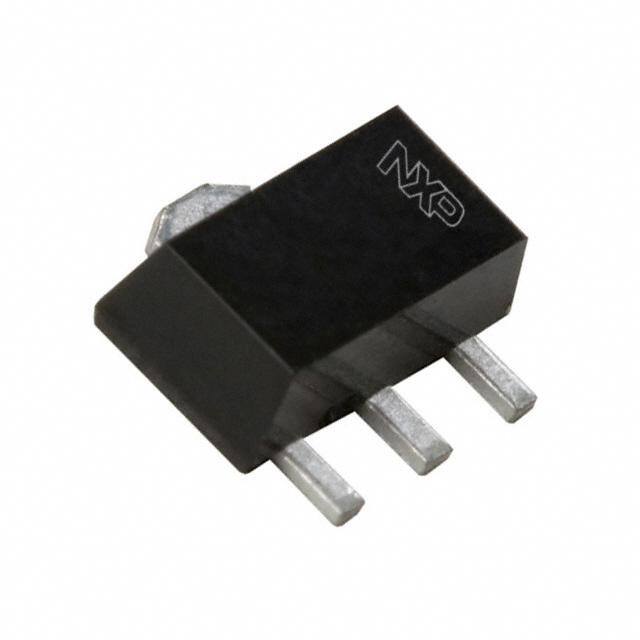
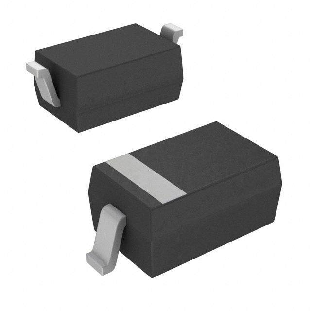
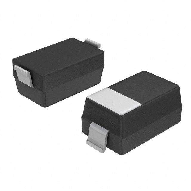
ICGOO电子元器件商城为您提供BZV49-C18,115由NXP Semiconductors设计生产,在icgoo商城现货销售,并且可以通过原厂、代理商等渠道进行代购。 BZV49-C18,115价格参考¥1.77-¥1.77。NXP SemiconductorsBZV49-C18,115封装/规格:二极管 - 齐纳 - 单, Zener Diode 18V 1W ±5% 表面贴装 SOT-89。您可以下载BZV49-C18,115参考资料、Datasheet数据手册功能说明书,资料中有BZV49-C18,115 详细功能的应用电路图电压和使用方法及教程。
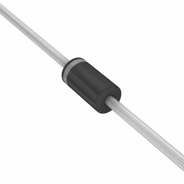
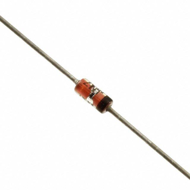
Nexperia USA Inc. 是一家知名的半导体制造商,其型号为 BZV49-C18,115 的器件是一款 齐纳二极管(Zener Diode),属于单路齐纳二极管类别。该器件主要应用于电压调节、稳压及电压参考等电路中。

该器件的典型应用场景包括:

1. 电源管理电路:用于低压直流电源中,提供稳定的参考电压,确保输出电压维持在设定值。
2. 电压监测电路:在电池供电设备中,用于检测电池电压是否在安全范围内,防止过压或欠压损坏设备。
3. 信号调理电路:在模拟电路中作为电压参考源,为运算放大器、比较器等提供稳定基准电压。
4. 保护电路:用于过压保护(OVP)电路中,限制输入电压,防止后级电路受到高压损坏。
5. 工业控制系统:广泛应用于工业自动化设备中的传感器供电、信号转换模块中,确保系统稳定性与精度。

该器件封装为DO-41,具有良好的稳定性和可靠性,适用于广泛的工业和消费类电子产品中。
| 参数 | 数值 |
| 产品目录 | |
| 描述 | DIODE ZENER 18V 1W SOT89稳压二极管 DIODE ZENER 5 PCT |
| 产品分类 | 单二极管/齐纳分离式半导体 |
| 品牌 | NXP Semiconductors |
| 产品手册 | |
| 产品图片 |
|
| rohs | 符合RoHS无铅 / 符合限制有害物质指令(RoHS)规范要求 |
| 产品系列 | 二极管与整流器,稳压二极管,NXP Semiconductors BZV49-C18,115- |
| 数据手册 | |
| 产品型号 | BZV49-C18,115 |
| PCN封装 | |
| PCN设计/规格 | |
| 不同If时的电压-正向(Vf) | 1V @ 50mA |
| 不同 Vr时的电流-反向漏电流 | 50nA @ 12.6V |
| 产品种类 | |
| 供应商器件封装 | SOT-89-3 |
| 其它名称 | 568-6831-6 |
| 功率-最大值 | 1W |
| 功率耗散 | 1 W |
| 包装 | Digi-Reel® |
| 商标 | NXP Semiconductors |
| 安装类型 | 表面贴装 |
| 安装风格 | SMD/SMT |
| 容差 | ±5% |
| 封装 | Reel |
| 封装/外壳 | TO-243AA |
| 封装/箱体 | SOT-89 |
| 工作温度 | -65°C ~ 150°C |
| 工厂包装数量 | 1000 |
| 最大反向漏泄电流 | 50 nA |
| 最大工作温度 | + 150 C |
| 最大齐纳阻抗 | 45 Ohms |
| 最小工作温度 | - 65 C |
| 标准包装 | 1 |
| 电压-齐纳(标称值)(Vz) | 18V |
| 电压容差 | 5 % |
| 电压温度系数 | 14.4 mV/K |
| 配置 | Single Dual Anode |
| 阻抗(最大值)(Zzt) | 45 欧姆 |
| 零件号别名 | BZV49-C18 T/R |
| 齐纳电压 | 17.95 V |

SOT89.jpg)


- 商务部:美国ITC正式对集成电路等产品启动337调查
- 曝三星4nm工艺存在良率问题 高通将骁龙8 Gen1或转产台积电
- 太阳诱电将投资9.5亿元在常州建新厂生产MLCC 预计2023年完工
- 英特尔发布欧洲新工厂建设计划 深化IDM 2.0 战略
- 台积电先进制程称霸业界 有大客户加持明年业绩稳了
- 达到5530亿美元!SIA预计今年全球半导体销售额将创下新高
- 英特尔拟将自动驾驶子公司Mobileye上市 估值或超500亿美元
- 三星加码芯片和SET,合并消费电子和移动部门,撤换高东真等 CEO
- 三星电子宣布重大人事变动 还合并消费电子和移动部门
- 海关总署:前11个月进口集成电路产品价值2.52万亿元 增长14.8%


PDF Datasheet 数据手册内容提取
Important notice Dear Customer, On 7 February 2017 the former NXP Standard Product business became a new company with the tradename Nexperia. Nexperia is an industry leading supplier of Discrete, Logic and PowerMOS semiconductors with its focus on the automotive, industrial, computing, consumer and wearable application markets In data sheets and application notes which still contain NXP or Philips Semiconductors references, use the references to Nexperia, as shown below. Instead of http://www.nxp.com, http://www.philips.com/ or http://www.semiconductors.philips.com/, use http://www.nexperia.com Instead of sales.addresses@www.nxp.com or sales.addresses@www.semiconductors.philips.com, use salesaddresses@nexperia.com (email) Replace the copyright notice at the bottom of each page or elsewhere in the document, depending on the version, as shown below: - © NXP N.V. (year). All rights reserved or © Koninklijke Philips Electronics N.V. (year). All rights reserved Should be replaced with: - © Nexperia B.V. (year). All rights reserved. If you have any questions related to the data sheet, please contact our nearest sales office via e-mail or telephone (details via salesaddresses@nexperia.com). Thank you for your cooperation and understanding, Kind regards, Team Nexperia
DISCRETE SEMICONDUCTORS DATA SHEET dbook, halfpage M3D109 BZV49 series Voltage regulator diodes Product data sheet 2005 Feb 03 Supersedes data of 1999 May 11
NXP Semiconductors Product data sheet Voltage regulator diodes BZV49 series FEATURES PINNING • Total power dissipation: max. 1 W PIN DESCRIPTION • Tolerance series: approx. ±5% 1 anode • Working voltage range: nom. 2.4 to 75 V (E24 range) 2 cathode • Non-repetitive peak reverse power dissipation: 3 anode max. 40 W. APPLICATIONS • General regulation functions. 1 3 DESCRIPTION Medium-power voltage regulator diodes in a SOT89 2 plastic SMD package. 3 2 1 sym096 The diodes are available in the normalized E24 approx. ±5% tolerance range. The series consists of 37 types with nominal working voltages from 2.4 to 75 V (BZV49-C2V4 to BZV49-C75). Fig.1 Simplified outline (SOT89) and symbol. ORDERING INFORMATION PACKAGE TYPE NUMBER NAME DESCRIPTION VERSION BZV49-C2V4 to SC-62 plastic surface mounted package; collector pad for good heat SOT89 BZV49-C75 transfer; 3 leads note 1 Note 1. The series consists of 37 types with nominal working voltages from 2.4 to 75 V (E24 range). MARKING TYPE MARKING TYPE MARKING TYPE MARKING TYPE MARKING NUMBER CODE NUMBER CODE NUMBER CODE NUMBER CODE BZV49-C2V4 2Y4 BZV49-C6V2 6Y2 BZV49-C16 16Y BZV49-C43 43Y BZV49-C2V7 2Y7 BZV49-C6V8 6Y8 BZV49-C18 18Y BZV49-C47 47Y BZV49-C3V0 3Y0 BZV49-C7V5 7Y5 BZV49-C20 20Y BZV49-C51 51Y BZV49-C3Y3 3Y3 BZV49-C8V2 8Y2 BZV49-C22 22Y BZV49-C56 56Y BZV49-C3V6 3Y6 BZV49-C9V1 9Y1 BZV49-C24 24Y BZV49-C62 62Y BZV49-C3V9 3Y9 BZV49-C10 10Y BZV49-C27 27Y BZV49-C68 68Y BZV49-C4V3 4Y3 BZV49-C11 11Y BZV49-C30 30Y BZV49-C75 75Y BZV49-C4V7 4Y7 BZV49-C12 12Y BZV49-C33 33Y − − BZV49-C5V1 5Y1 BZV49-C13 13Y BZV49-C36 36Y − − BZV49-C5V6 5Y6 BZV49-C15 15Y BZV49-C39 39Y − − 2005 Feb 03 2
NXP Semiconductors Product data sheet Voltage regulator diodes BZV49 series LIMITING VALUES In accordance with the Absolute Maximum Rating System (IEC 60134). SYMBOL PARAMETER CONDITIONS MIN. MAX. UNIT I continuous forward current − 250 mA F I non-repetitive peak reverse current t = 100 μs; square wave; see Table ZSM p T = 25 °C prior to surge “Per type” j P total power dissipation T = 25 °C; note 1 − 1 W tot amb P non-repetitive peak reverse power t = 100 μs; square wave; − 40 W ZSM p dissipation T = 25 °C prior to surge; see Fig.2 j T storage temperature −65 +150 °C stg T junction temperature − 150 °C j Note 1. Device mounted on a ceramic substrate; area = 2.5 cm2; thickness = 0.7 mm. ELECTRICAL CHARACTERISTICS Total series T = 25 °C unless otherwise specified. amb SYMBOL PARAMETER CONDITIONS MAX. UNIT V forward voltage I = 50 mA; see Fig.3 1 V F F 2005 Feb 03 3
2 Per type N 0 X 05 Tj = 25 °C unless otherwise specified. V P F o S eb WORKING DIFFERENTIAL TEMP. COEFF. TEST DIODE CAP. REVERSE NON-REPETITIVE PEAK lta em 03 VOLTAGE RESISTANCE SZ (mV/K) CURRENT Cd (pF) CURRENT at REVERSE CURRENT ge ico BCZXVX4X9- aVt ZI Z(tVes) t ardt iIf Z(tΩes)t see Faitg IsZ t4e satnd 5 IZtest (mA) aat tf V=R 1 = M 0H Vz; VROEVLTEARGSEE aTt tIpZ S= M= 1 (20A50) °μCs; reg nducto IR (μA) VR amb ula rs MIN. MAX. TYP. MAX. MIN. TYP. MAX. MAX. MAX. (V) MAX. to r 2V4 2.2 2.6 70 100 −3.5 −1.6 0 5 450 50 1.0 6.0 d i 2V7 2.5 2.9 75 100 −3.5 −2.0 0 5 450 20 1.0 6.0 o d 3V0 2.8 3.2 80 95 −3.5 −2.1 0 5 450 10 1.0 6.0 e s 3V3 3.1 3.5 85 95 −3.5 −2.4 0 5 450 5 1.0 6.0 3V6 3.4 3.8 85 90 −3.5 −2.4 0 5 450 5 1.0 6.0 3V9 3.7 4.1 85 90 −3.5 −2.5 0 5 450 3 1.0 6.0 4V3 4.0 4.6 80 90 −3.5 −2.5 0 5 450 3 1.0 6.0 4V7 4.4 5.0 50 80 −3.5 −1.4 +0.2 5 300 3 2.0 6.0 5V1 4.8 5.4 40 60 −2.7 −0.8 +1.2 5 300 2 2.0 6.0 4 5V6 5.2 6.0 15 40 −2.0 +1.2 +2.5 5 300 1 2.0 6.0 6V2 5.8 6.6 6 10 0.4 2.3 3.7 5 200 3 4.0 6.0 6V8 6.4 7.2 6 15 1.2 3.0 4.5 5 200 2 4.0 6.0 7V5 7.0 7.9 6 15 2.5 4.0 5.3 5 150 1 5.0 4.0 8V2 7.7 8.7 6 15 3.2 4.6 6.2 5 150 0.7 5.0 4.0 9V1 8.5 9.6 6 15 3.8 5.5 7.0 5 150 0.5 6.0 3.0 10 9.4 10.6 8 20 4.5 6.4 8.0 5 90 0.2 7.0 3.0 11 10.4 11.6 10 20 5.4 7.4 9.0 5 85 0.1 8.0 2.5 12 11.4 12.7 10 25 6.0 8.4 10.0 5 85 0.1 8.0 2.5 13 12.4 14.1 10 30 7.0 9.4 11.0 5 80 0.1 8.0 2.5 15 13.8 15.6 10 30 9.2 11.4 13.0 5 75 0.05 10.5 2.0 B Z 16 15.3 17.1 10 40 10.4 12.4 14.0 5 75 0.05 11.2 1.5 V P r 18 16.8 19.1 10 45 12.4 14.4 16.0 5 70 0.05 12.6 1.5 4 od 9 u 20 18.8 21.2 15 55 14.4 16.4 18.0 5 60 0.05 14.0 1.5 c 22 20.8 23.3 20 55 16.4 18.4 20.0 5 60 0.05 15.4 1.25 se t da ri ta 24 22.8 25.6 25 70 18.4 20.4 22.0 5 55 0.05 16.8 1.25 e s s h e e t
2 N 0 WORKING DIFFERENTIAL TEMP. COEFF. TEST DIODE CAP. REVERSE NON-REPETITIVE PEAK X 05 F VOLTAGE RESISTANCE SZ (mV/K) CURRENT Cd (pF) CURRENT at REVERSE CURRENT Vo P S eb BZV49- VZ (V) rdif (Ω) at IZtest IZtest (mA) at f = 1 MHz; REVERSE IZSM (A) lta em 03 CXXX at IZtest at IZtest see Figs 4 and 5 at VR = 0 V IR V(μOAL)TAGEVR aTt atmp b= = 1 2050 °μCs; ge re iconduc MIN. MAX. TYP. MAX. MIN. TYP. MAX. MAX. MAX. (V) MAX. g to u rs 27 25.1 28.9 25 80 21.4 23.4 25.3 2 50 0.05 18.9 1.0 la t 30 28.0 32.0 30 80 24.4 26.6 29.4 2 50 0.05 21.0 1.0 o r 33 31.0 35.0 35 80 27.4 29.7 33.4 2 45 0.05 23.1 0.9 d i o 36 34.0 38.0 35 90 30.4 33.0 37.4 2 45 0.05 25.2 0.8 d e 39 37.0 41.0 40 130 33.4 36.4 41.2 2 45 0.05 27.3 0.7 s 43 40.0 46.0 45 150 37.6 41.2 46.6 2 40 0.05 30.1 0.6 47 44.0 50.0 50 170 42.0 46.1 51.8 2 40 0.05 32.9 0.5 51 48.0 54.0 60 180 46.6 51.0 57.2 2 40 0.05 35.7 0.4 56 52.0 60.0 70 200 52.2 57.0 63.8 2 40 0.05 39.2 0.3 62 58.0 66.0 80 215 58.8 64.4 71.6 2 35 0.05 43.4 0.3 68 64.0 72.0 90 240 65.6 71.7 79.8 2 35 0.05 47.6 0.25 5 75 70.0 79.0 95 255 73.4 80.2 88.6 2 35 0.05 52.5 0.2 B Z V P r 4 o d 9 u c se t da ri ta e s s h e e t
NXP Semiconductors Product data sheet Voltage regulator diodes BZV49 series THERMAL CHARACTERISTICS SYMBOL PARAMETER CONDITIONS VALUE UNIT R thermal resistance from junction to tie-point 15 K/W th(j-tp) R thermal resistance from junction to ambient note 1 125 K/W th(j-a) Note 1. Device mounted on a ceramic substrate; area = 2.5 cm2; thickness = 0.7 mm. GRAPHICAL DATA 103 MBG801 300 MBG781 handbook, halfpage handbook, halfpage PZSM IF (W) (mA) 102 200 (1) 10 100 (2) 1 0 10−1 1 duration (ms) 10 0.6 0.8 VF (V) 1 (1) Tj = 25 °C (prior to surge). (2) Tj = 150 °C (prior to surge). Tj = 25 °C. Fig.2 Maximum permissible non-repetitive peak Fig.3 Forward current as a function of forward reverse power dissipation versus duration. voltage; typical values. 2005 Feb 03 6
NXP Semiconductors Product data sheet Voltage regulator diodes BZV49 series MBG927 1 handbook, full pagewidth SZ 4V3 (mV/K) 3V9 0 3V6 3V3 −1 3V0 −2 2V7 2V4 −3 10-3 10-2 10-1 IZ (A) 1 BZV49-C2V4 to C4V3. Tj = 25 to 150 °C. Fig.4 Temperature coefficient as a function of working current; typical values. MBG924 10 handbook, halfpage SZ (mV/K) 10 9V1 5 8V2 7V5 6V8 6V2 5V6 5V1 0 4V7 −5 0 4 8 12 16 20 IZ (mA) BZV49-C4V7 to C10. Tj = 25 to 150 °C. Fig.5 Temperature coefficient as a function of working current; typical values. 2005 Feb 03 7
NXP Semiconductors Product data sheet Voltage regulator diodes BZV49 series PACKAGE OUTLINE Plastic surface-mounted package; collector pad for good heat transfer; 3 leads SOT89 D B A bp3 E HE Lp 1 2 3 bp2 c w M bp1 e1 e 0 2 4 mm scale DIMENSIONS (mm are the original dimensions) UNIT A bp1 bp2 bp3 c D E e e1 HE Lp w 1.6 0.48 0.53 1.8 0.44 4.6 2.6 4.25 1.2 mm 3.0 1.5 0.13 1.4 0.35 0.40 1.4 0.23 4.4 2.4 3.75 0.8 OUTLINE REFERENCES EUROPEAN ISSUE DATE VERSION IEC JEDEC JEITA PROJECTION 04-08-03 SOT89 TO-243 SC-62 06-03-16 2005 Feb 03 8
NXP Semiconductors Product data sheet Voltage regulator diodes BZV49 series DATA SHEET STATUS DOCUMENT PRODUCT DEFINITION STATUS(1) STATUS(2) Objective data sheet Development This document contains data from the objective specification for product development. Preliminary data sheet Qualification This document contains data from the preliminary specification. Product data sheet Production This document contains the product specification. Notes 1. Please consult the most recently issued document before initiating or completing a design. 2. The product status of device(s) described in this document may have changed since this document was published and may differ in case of multiple devices. The latest product status information is available on the Internet at URL http://www.nxp.com. DISCLAIMERS above those given in the Characteristics sections of this document is not implied. Exposure to limiting values for General ⎯ Information in this document is believed to be extended periods may affect device reliability. accurate and reliable. However, NXP Semiconductors does not give any representations or warranties, Terms and conditions of sale ⎯ NXP Semiconductors expressed or implied, as to the accuracy or completeness products are sold subject to the general terms and of such information and shall have no liability for the conditions of commercial sale, as published at consequences of use of such information. http://www.nxp.com/profile/terms, including those pertaining to warranty, intellectual property rights Right to make changes ⎯ NXP Semiconductors infringement and limitation of liability, unless explicitly reserves the right to make changes to information otherwise agreed to in writing by NXP Semiconductors. In published in this document, including without limitation case of any inconsistency or conflict between information specifications and product descriptions, at any time and in this document and such terms and conditions, the latter without notice. This document supersedes and replaces all will prevail. information supplied prior to the publication hereof. No offer to sell or license ⎯ Nothing in this document Suitability for use ⎯ NXP Semiconductors products are may be interpreted or construed as an offer to sell products not designed, authorized or warranted to be suitable for that is open for acceptance or the grant, conveyance or use in medical, military, aircraft, space or life support implication of any license under any copyrights, patents or equipment, nor in applications where failure or malfunction other industrial or intellectual property rights. of an NXP Semiconductors product can reasonably be expected to result in personal injury, death or severe Export control ⎯ This document as well as the item(s) property or environmental damage. NXP Semiconductors described herein may be subject to export control accepts no liability for inclusion and/or use of NXP regulations. Export might require a prior authorization from Semiconductors products in such equipment or national authorities. applications and therefore such inclusion and/or use is at Quick reference data ⎯ The Quick reference data is an the customer’s own risk. extract of the product data given in the Limiting values and Applications ⎯ Applications that are described herein for Characteristics sections of this document, and as such is any of these products are for illustrative purposes only. not complete, exhaustive or legally binding. NXP Semiconductors makes no representation or warranty that such applications will be suitable for the specified use without further testing or modification. Limiting values ⎯ Stress above one or more limiting values (as defined in the Absolute Maximum Ratings System of IEC 60134) may cause permanent damage to the device. Limiting values are stress ratings only and operation of the device at these or any other conditions 2005 Feb 03 9
NXP Semiconductors Customer notification This data sheet was changed to reflect the new company name NXP Semiconductors, including new legal definitions and disclaimers. No changes were made to the technical content, except for package outline drawings which were updated to the latest version. Contact information For additional information please visit: http://www.nxp.com For sales offices addresses send e-mail to: salesaddresses@nxp.com © NXP B.V. 2009 All rights are reserved. Reproduction in whole or in part is prohibited without the prior written consent of the copyright owner. The information presented in this document does not form part of any quotation or contract, is believed to be accurate and reliable and may be changed without notice. No liability will be accepted by the publisher for any consequence of its use. Publication thereof does not convey nor imply any license under patent- or other industrial or intellectual property rights. Printed in The Netherlands R76/04/pp10 Date of release: 2005 Feb 03 Document order number: 9397 750 13926