ICGOO在线商城 > 分立半导体产品 > 二极管 - 齐纳 - 单 > BZT52C11S-7-F
 Datasheet下载
- 型号: BZT52C11S-7-F
- 制造商: Diodes Inc.
- 库位|库存: xxxx|xxxx
- 要求:
| 数量阶梯 | 香港交货 | 国内含税 |
| +xxxx | $xxxx | ¥xxxx |
查看当月历史价格
查看今年历史价格
BZT52C11S-7-F产品简介:
ICGOO电子元器件商城为您提供BZT52C11S-7-F由Diodes Inc.设计生产,在icgoo商城现货销售,并且可以通过原厂、代理商等渠道进行代购。 BZT52C11S-7-F价格参考¥0.17-¥0.17。Diodes Inc.BZT52C11S-7-F封装/规格:二极管 - 齐纳 - 单, Zener Diode 11V 200mW ±5% Surface Mount SOD-323。您可以下载BZT52C11S-7-F参考资料、Datasheet数据手册功能说明书,资料中有BZT52C11S-7-F 详细功能的应用电路图电压和使用方法及教程。
BZT52C11S-7-F 是由 Diodes Incorporated 推出的一款单齐纳二极管,广泛应用于各类电子电路中,主要用于电压参考和稳压功能。该器件的齐纳电压为11V,适用于需要稳定电压输出的小功率电路设计。

其主要应用场景包括:

1. 电源电路:用于提供稳定的参考电压或实现简单的稳压功能,如在DC-DC转换器、电池充电器中作为反馈网络的一部分。

2. 保护电路:可用于过压保护电路中,限制输入电压,保护后续敏感器件免受高压损坏。

3. 信号调理电路:在模拟电路中用作电压钳位或电平调整,确保信号在特定范围内工作。

4. 嵌入式系统与工业控制:在工业控制系统、传感器模块中提供基准电压,保障测量精度和稳定性。

5. 消费类电子产品:如智能家电、LED驱动等对成本和空间有要求的应用场景。

该器件采用SOD-123封装,体积小、响应速度快,适合高密度PCB布局,且具备良好的热稳定性和可靠性,适用于各种中低端电压调节需求。
| 参数 | 数值 |
| 产品目录 | |
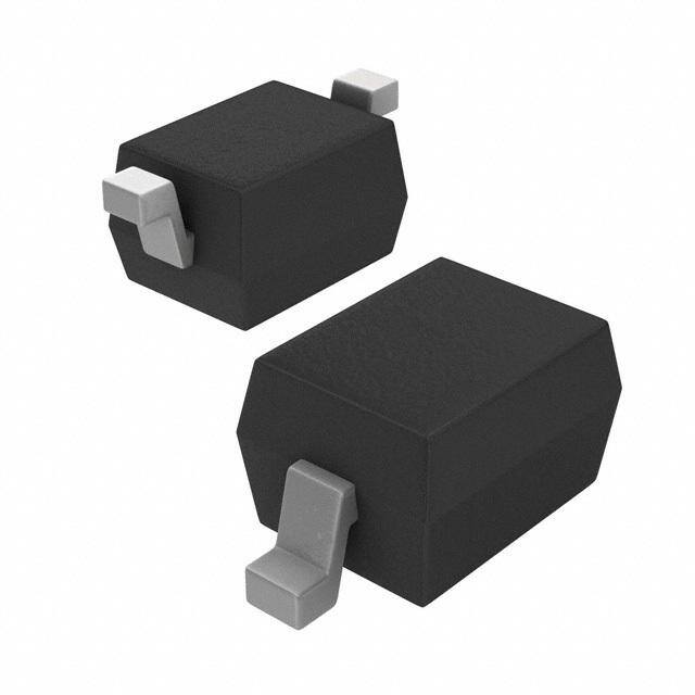
| 描述 | DIODE ZENER 11V 200MW SOD323稳压二极管 11V 200mW |
| 产品分类 | 单二极管/齐纳分离式半导体 |
| 品牌 | Diodes Incorporated |
| 产品手册 | |
| 产品图片 |
|
| rohs | 符合RoHS无铅 / 符合限制有害物质指令(RoHS)规范要求 |
| 产品系列 | 二极管与整流器,稳压二极管,Diodes Incorporated BZT52C11S-7-F- |
| 数据手册 | |
| 产品型号 | BZT52C11S-7-F |
| PCN其它 | |
| PCN设计/规格 | |
| RoHS指令信息 | http://diodes.com/download/4349 |
| 不同If时的电压-正向(Vf) | 900mV @ 10mA |
| 不同 Vr时的电流-反向漏电流 | 100nA @ 8V |
| 产品目录绘图 |
|
| 产品目录页面 | |
| 产品种类 | |
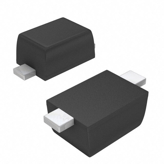
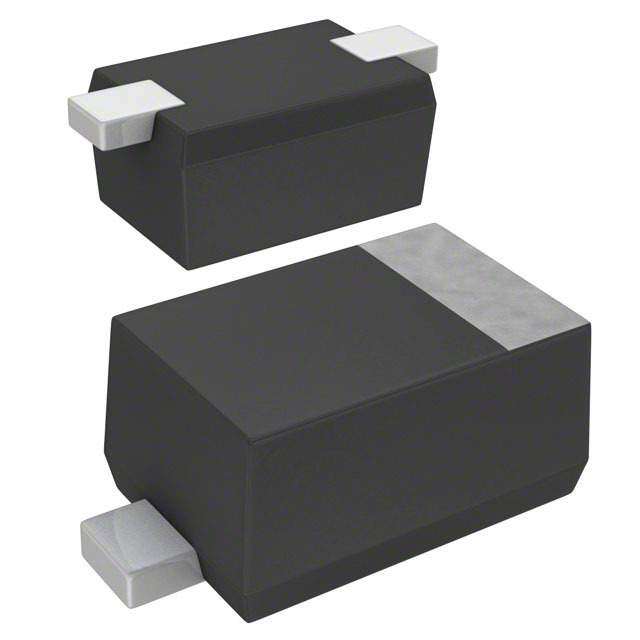
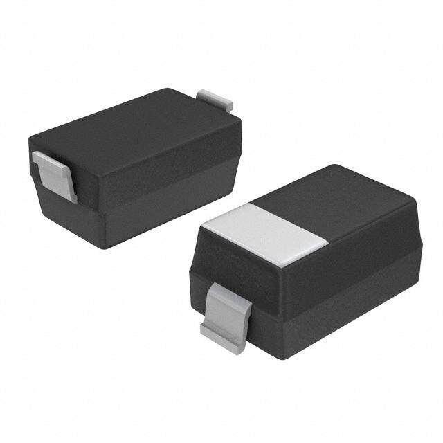
| 供应商器件封装 | SOD-323 |
| 其它名称 | BZT52C11S-FDIDKR |
| 功率-最大值 | 200mW |
| 功率耗散 | 200 mW |
| 包装 | Digi-Reel® |
| 商标 | Diodes Incorporated |
| 安装类型 | 表面贴装 |
| 安装风格 | SMD/SMT |
| 容差 | ±5% |
| 封装 | Reel |
| 封装/外壳 | SC-76,SOD-323 |
| 封装/箱体 | SOD-323 |
| 工作温度 | -65°C ~ 150°C |
| 工厂包装数量 | 3000 |
| 最大反向漏泄电流 | 100 nA |
| 最大工作温度 | + 150 C |
| 最大齐纳阻抗 | 20 Ohms |
| 最小工作温度 | - 65 C |
| 标准包装 | 1 |
| 电压-齐纳(标称值)(Vz) | 11V |
| 电压容差 | 5 % |
| 电压温度系数 | 7.2 mV/C |
| 系列 | BZT52C11S |
| 配置 | Single |
| 阻抗(最大值)(Zzt) | 20 欧姆 |
| 齐纳电压 | 11 V |
| 齐纳电流 | 5 mA |


- 商务部:美国ITC正式对集成电路等产品启动337调查
- 曝三星4nm工艺存在良率问题 高通将骁龙8 Gen1或转产台积电
- 太阳诱电将投资9.5亿元在常州建新厂生产MLCC 预计2023年完工
- 英特尔发布欧洲新工厂建设计划 深化IDM 2.0 战略
- 台积电先进制程称霸业界 有大客户加持明年业绩稳了
- 达到5530亿美元!SIA预计今年全球半导体销售额将创下新高
- 英特尔拟将自动驾驶子公司Mobileye上市 估值或超500亿美元
- 三星加码芯片和SET,合并消费电子和移动部门,撤换高东真等 CEO
- 三星电子宣布重大人事变动 还合并消费电子和移动部门
- 海关总署:前11个月进口集成电路产品价值2.52万亿元 增长14.8%

PDF Datasheet 数据手册内容提取
BZT52C2V0S - BZT52C39S SURFACE MOUNT ZENER DIODE Features Mechanical Data Planar Die Construction Case: SOD323 Small Surface Mount Package Case Material: Molded Plastic. Ideally Suited for Automated Assembly Processes UL Flammability Classification Rating 94V-0 Totally Lead-Free & Fully RoHS Compliant (Notes 1 & 2) Moisture Sensitivity: Level 1 per J-STD-020 Halogen and Antimony Free. “Green” Device (Notes 3 & 4) Terminals: Matte Tin Finish Annealed over Alloy 42 Leadframe Qualified to AEC-Q101 Standards for High Reliability (Lead Free Plating). Solderable per MIL-STD-202, Method 208 Polarity: Cathode Band Weight: 0.0049 grams (Approximate) SOD323 Top View Ordering Information (Note 5) Part Number Qualification Case Packaging (Type Number)-7-F* Commercial SOD323 3,000/Tape & Reel (Type Number)Q-7-F* Automotive SOD323 3,000/Tape & Reel *Add “-7-F” to the appropriate type number in Electrical Characteristics Table, example: 6.2V Zener – BZT52C6V2S-7-F. Notes: 1. No purposely added lead. Fully EU Directive 2002/95/EC (RoHS) & 2011/65/EU (RoHS 2) compliant. 2. See http://www.diodes.com/quality/lead_free.html for more information about Diodes Incorporated’s definitions of Halogen- and Antimony-free, "Green" and Lead-free. 3. Halogen- and Antimony-free "Green” products are defined as those which contain <900ppm bromine, <900ppm chlorine (<1500ppm total Br + Cl) and <1000ppm antimony compounds. 4. Product manufactured with Date Code V9 (week 33, 2008) and newer are built with Green Molding Compound. Products manufactured prior to Date Code V9 are built with Non-Green Molding Compound and may contain Halogens or Sb2O3 Fire Retardants. 5. For packaging details, go to our website at http://www.diodes.com/products/packages.html. Marking Information XX = Product Type Marking Code for XX = Product Type Marking Code for XX SAT (Shanghai Assembly / Test site) XX CAT (Chengdu Assembly / Test site) (See Electrical Characteristics Table) (See Electrical Characteristics Table) BZT52C2V0S - BZT52C39S 1 of 5 February 2017 Document number: DS30093 Rev. 20 - 2 www.diodes.com © Diodes Incorporated
BZT52C2V0S - BZT52C39S Maximum Ratings (@TA = +25°C, unless otherwise specified.) Single phase, half wave, 60Hz, resistive or inductive load. For capacitance load, derate current by 20%. Characteristic Symbol Value Unit Forward Voltage (Note 6) @IF = 10mA VF 0.9 V Thermal Characteristics Characteristic Symbol Value Unit Power Dissipation (Note 7) PD 200 mW Thermal Resistance, Junction to Ambient Air (Note 7) RJA 625 °C/W Operating and Storage Temperature Range TJ, TSTG -65 to +150 °C Electrical Characteristics (@TA = +25°C, unless otherwise specified.) Maximum Temperature Zener Voltage Maximum Zener Impedance Reverse Current Coefficient of Range (Note 4) f = 1kHz Marking (Note 6) Zener Voltage Type Number Code VZ @IZT IZT ZZT @IZT ZZK @IZK IZK IR @VR @ImZTV =/ °5Cm A Nom (V) Min (V) Max (V) (mA) Ω mA uA V Min Max BZT52C2V0S WY 2.0 1.91 2.09 5 100 600 1.0 150 1.0 -3.5 0 BZT52C2V4S WX 2.4 2.20 2.60 5 100 600 1.0 50 1.0 -3.5 0 BZT52C2V7S W1 2.7 2.5 2.9 5 100 600 1.0 20 1.0 -3.5 0 BZT52C3V0S W2 3.0 2.8 3.2 5 95 600 1.0 10 1.0 -3.5 0 BZT52C3V3S W3 3.3 3.1 3.5 5 95 600 1.0 5 1.0 -3.5 0 BZT52C3V6S W4 3.6 3.4 3.8 5 90 600 1.0 5 1.0 -3.5 0 BZT52C3V9S W5 3.9 3.7 4.1 5 90 600 1.0 3 1.0 -3.5 0 BZT52C4V3S W6 4.3 4.0 4.6 5 90 600 1.0 3 1.0 -3.5 0 BZT52C4V7S W7 4.7 4.4 5.0 5 80 500 1.0 2 2.0 -3.5 0.2 BZT52C5V1S W8 5.1 4.8 5.4 5 60 480 1.0 1 2.0 -2.7 1.2 BZT52C5V6S W9 5.6 5.2 6.0 5 40 400 1.0 3 2.0 -2.0 2.5 BZT52C6V2S WA 6.2 5.8 6.6 5 10 150 1.0 2 4.0 0.4 3.7 BZT52C6V8S WB 6.8 6.4 7.2 5 15 80 1.0 1 4.0 1.2 4.5 BZT52C7V5S WC 7.5 7.0 7.9 5 15 80 1.0 0.7 5.0 2.5 5.3 BZT52C8V2S WD 8.2 7.7 8.7 5 15 80 1.0 0.5 5.0 3.2 6.2 BZT52C9V1S WE 9.1 8.5 9.6 5 15 100 1.0 0.2 6.0 3.8 7.0 BZT52C10S WF 10 9.4 10.6 5 20 150 1.0 0.1 7.0 4.5 8.0 BZT52C11S WG 11 10.4 11.6 5 20 150 1.0 0.1 8.0 5.4 9.0 BZT52C12S WH 12 11.4 12.7 5 25 150 1.0 0.1 8.0 6.0 10.0 BZT52C13S WI 13 12.4 14.1 5 30 170 1.0 0.1 8.0 7.0 11.0 BZT52C15S WJ 15 13.8 15.6 5 30 200 1.0 0.1 10.5 9.2 13.0 BZT52C16S WK 16 15.3 17.1 5 40 200 1.0 0.1 11.2 10.4 — BZT52C18S WL 18 16.8 19.1 5 45 225 1.0 0.1 12.6 12.4 — BZT52C20S WM 20 18.8 21.2 5 55 225 1.0 0.1 14.0 14.4 — BZT52C22S WN 22 20.8 23.3 5 55 250 1.0 0.1 15.4 16.4 — BZT52C24S WO 24 22.8 25.6 5 70 250 1.0 0.1 16.8 18.4 — BZT52C27S WP 27 25.1 28.9 2 80 300 0.5 0.1 18.9 21.4 — BZT52C30S WQ 30 28.0 32.0 2 80 300 0.5 0.1 21.0 24.4 — BZT52C33S WR 33 31.0 35.0 2 80 325 0.5 0.1 23.1 27.4 — BZT52C36S WS 36 34.0 38.0 2 90 350 0.5 0.1 25.2 30.4 — BZT52C39S WT 39 37.0 41.0 2 130 350 0.5 0.1 27.3 33.4 — Notes: 6. Short duration pulse test used to minimize self-heating effect. 7. Part mounted on FR-4 PC board with recommended pad layout, as per http://www.diodes.com/package-outlines.html. BZT52C2V0S - BZT52C39S 2 of 5 February 2017 Document number: DS30093 Rev. 20 - 2 www.diodes.com © Diodes Incorporated
BZT52C2V0S - BZT52C39S 300 50 TJ = 25°C C2V7 C3V9 C5V6 Note 7 C2V0 C3V3 C4V7 C6V8 W) 40 TION (m200 NT (mA) 30 C8V2 A E P R SI R S U DI C R R 20 E E W100 N , POD I, ZEZ10Test5 C.0umrreAnt IZ P 0 0 0 40 80 120 160 200 0 1 2 3 4 5 6 7 8 9 10 T , AMBIENT TEMPERATURE, °C V , ZENER VOLTAGE (V) A Z Fig. 1 Power Derating Curve Fig. 2 Typical Zener Breakdown Characteristics 30 1,000 TJ = 25°C C10 T = 25 °C J C12 F) VR = 1V p T (mA) 20 C15 NCE ( VR = 2V REN CITA R C18 A100 U P R C L CA VR = 1V E C22 A N 10 T E C27 O Z Test current IZ C39 T , Z 5mA C33 C36 , T V = 2V I C R 10 0 0 10 20 30 40 1 10 100 V , ZENER VOLTAGE (V) V , NOMINAL ZENER VOLTAGE (V) Z Z Fig. 3 Typical Zener Breakdown Characteristics Fig. 4 Typical Total Capacitance vs. Nominal Zener Voltage BZT52C2V0S - BZT52C39S 3 of 5 February 2017 Document number: DS30093 Rev. 20 - 2 www.diodes.com © Diodes Incorporated
BZT52C2V0S - BZT52C39S Package Outline Dimensions Please see http://www.diodes.com/package-outlines.html for the latest version. SOD323 A2 A1 SOD323 Dim Min Max Typ A1 -- 0.10 0.05 a A2 1.00 1.10 1.05 c L b 0.25 0.35 0.30 He c 0.10 0.15 0.11 E D 1.20 1.40 1.30 E 1.60 1.80 1.70 He 2.30 2.70 2.50 L 0.20 0.40 0.30 a 0º 8º -- b D All Dimensions in mm Suggested Pad Layout Please see http://www.diodes.com/package-outlines.html for the latest version. SOD323 X1 Dimensions Value (in mm) X 0.590 Y X1 2.700 Y 0.450 X BZT52C2V0S - BZT52C39S 4 of 5 February 2017 Document number: DS30093 Rev. 20 - 2 www.diodes.com © Diodes Incorporated
BZT52C2V0S - BZT52C39S IMPORTANT NOTICE DIODES INCORPORATED MAKES NO WARRANTY OF ANY KIND, EXPRESS OR IMPLIED, WITH REGARDS TO THIS DOCUMENT, INCLUDING, BUT NOT LIMITED TO, THE IMPLIED WARRANTIES OF MERCHANTABILITY AND FITNESS FOR A PARTICULAR PURPOSE (AND THEIR EQUIVALENTS UNDER THE LAWS OF ANY JURISDICTION). Diodes Incorporated and its subsidiaries reserve the right to make modifications, enhancements, improvements, corrections or other changes without further notice to this document and any product described herein. Diodes Incorporated does not assume any liability arising out of the application or use of this document or any product described herein; neither does Diodes Incorporated convey any license under its patent or trademark rights, nor the rights of others. Any Customer or user of this document or products described herein in such applications shall assume all risks of such use and will agree to hold Diodes Incorporated and all the companies whose products are represented on Diodes Incorporated website, harmless against all damages. Diodes Incorporated does not warrant or accept any liability whatsoever in respect of any products purchased through unauthorized sales channel. Should Customers purchase or use Diodes Incorporated products for any unintended or unauthorized application, Customers shall indemnify and hold Diodes Incorporated and its representatives harmless against all claims, damages, expenses, and attorney fees arising out of, directly or indirectly, any claim of personal injury or death associated with such unintended or unauthorized application. Products described herein may be covered by one or more United States, international or foreign patents pending. Product names and markings noted herein may also be covered by one or more United States, international or foreign trademarks. This document is written in English but may be translated into multiple languages for reference. Only the English version of this document is the final and determinative format released by Diodes Incorporated. LIFE SUPPORT Diodes Incorporated products are specifically not authorized for use as critical components in life support devices or systems without the express written approval of the Chief Executive Officer of Diodes Incorporated. As used herein: A. Life support devices or systems are devices or systems which: 1. are intended to implant into the body, or 2. support or sustain life and whose failure to perform when properly used in accordance with instructions for use provided in the labeling can be reasonably expected to result in significant injury to the user. B. A critical component is any component in a life support device or system whose failure to perform can be reasonably expected to cause the failure of the life support device or to affect its safety or effectiveness. Customers represent that they have all necessary expertise in the safety and regulatory ramifications of their life support devices or systems, and acknowledge and agree that they are solely responsible for all legal, regulatory and safety-related requirements concerning their products and any use of Diodes Incorporated products in such safety-critical, life support devices or systems, notwithstanding any devices- or systems-related information or support that may be provided by Diodes Incorporated. Further, Customers must fully indemnify Diodes Incorporated and its representatives against any damages arising out of the use of Diodes Incorporated products in such safety-critical, life support devices or systems. Copyright © 2017, Diodes Incorporated www.diodes.com BZT52C2V0S - BZT52C39S 5 of 5 February 2017 Document number: DS30093 Rev. 20 - 2 www.diodes.com © Diodes Incorporated