 Datasheet下载
- 型号: BZA968AVL,115
- 制造商: NXP Semiconductors
- 库位|库存: xxxx|xxxx
- 要求:
| 数量阶梯 | 香港交货 | 国内含税 |
| +xxxx | $xxxx | ¥xxxx |
查看当月历史价格
查看今年历史价格
BZA968AVL,115产品简介:
ICGOO电子元器件商城为您提供BZA968AVL,115由NXP Semiconductors设计生产,在icgoo商城现货销售,并且可以通过原厂、代理商等渠道进行代购。 BZA968AVL,115价格参考。NXP SemiconductorsBZA968AVL,115封装/规格:TVS - 二极管, 。您可以下载BZA968AVL,115参考资料、Datasheet数据手册功能说明书,资料中有BZA968AVL,115 详细功能的应用电路图电压和使用方法及教程。
型号为 BZA968AVL,115 的 TVS(瞬态电压抑制)二极管,由 NXP USA Inc. 生产,主要用于电路中对敏感电子元件进行过电压保护。其应用场景主要包括以下几个方面:

1. 电源线路保护:用于防止因雷击、电感负载切换或静电放电(ESD)引起的瞬态过电压损坏电源模块或供电系统。

2. 通信接口保护:广泛应用于RS-485、CAN总线、USB、HDMI等通信接口,保护数据传输线路免受瞬态电压冲击。

3. 消费类电子产品:如电视、机顶盒、家庭影院系统等,用于保护内部集成电路免受静电和瞬态电压损害。

4. 汽车电子系统:在车载电子控制单元(ECU)、车载娱乐系统、传感器模块中提供过电压保护,尤其适用于要求高可靠性的汽车应用场景。

5. 工业控制系统:用于PLC、工业计算机、传感器和执行器接口,提升系统在恶劣工业环境下的稳定性和耐用性。

该器件具有响应速度快、钳位电压低、可靠性高等特点,适合用于需要对敏感电路进行高效瞬态电压抑制的场合。
| 参数 | 数值 |
| 产品目录 | |
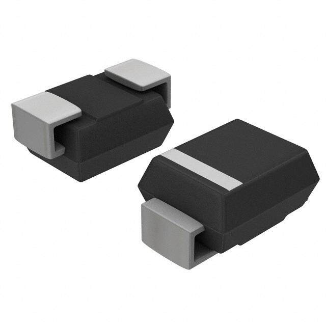
| 描述 | TVS DIODE 6.8VWM SOT665TVS二极管阵列 DIODE ARRAY TAPE-7 |
| 产品分类 | |
| 品牌 | NXP Semiconductors |
| 产品手册 | |
| 产品图片 |
|
| rohs | 符合RoHS无铅 / 符合限制有害物质指令(RoHS)规范要求 |
| 产品系列 | 二极管与整流器,TVS二极管,TVS二极管阵列,NXP Semiconductors BZA968AVL,115- |
| 数据手册 | |
| 产品型号 | BZA968AVL,115 |
| PCN封装 | |
| PCN设计/规格 | |
| PCN过时产品 | |
| 不同频率时的电容 | 16pF @ 1MHz |
| 产品种类 | TVS二极管阵列 |
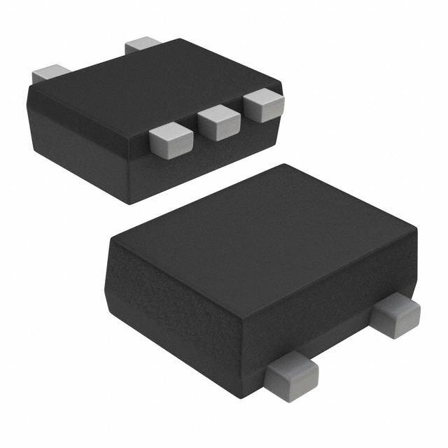
| 供应商器件封装 | SOT-665 |
| 其它名称 | 568-7021-6 |
| 功率-峰值脉冲 | 6W |
| 包装 | 剪切带 (CT) |
| 单向通道 | 4 |
| 双向通道 | - |
| 商标 | NXP Semiconductors |
| 安装类型 | 表面贴装 |
| 安装风格 | SMD/SMT |
| 封装 | Reel |
| 封装/外壳 | SOT-665 |
| 封装/箱体 | SOT-665 |
| 尺寸 | 1.3(Max) mm W x 1.7(Max) mm L |
| 峰值浪涌电流 | 0.8 A |
| 峰值脉冲功率耗散 | 6 W |
| 工作温度 | - |
| 工作电压 | 6.8 V |
| 工厂包装数量 | 4000 |
| 应用 | 通用 |
| 最大工作温度 | + 150 C |
| 最小工作温度 | - 65 C |
| 极性 | Unidirectional |
| 标准包装 | 1 |
| 电压-击穿(最小值) | - |
| 电压-反向关态(典型值) | 6.8V |
| 电压-箝位(最大值)@Ipp | - |
| 电容 | 16 pF |
| 电流-峰值脉冲(10/1000µs) | - |
| 电源线路保护 | 无 |
| 端接类型 | SMD/SMT |
| 类型 | 齐纳 |
| 系列 | BZA900AVL |
| 通道 | 4 Channels |
| 零件号别名 | BZA968AVL T/R |


- 商务部:美国ITC正式对集成电路等产品启动337调查
- 曝三星4nm工艺存在良率问题 高通将骁龙8 Gen1或转产台积电
- 太阳诱电将投资9.5亿元在常州建新厂生产MLCC 预计2023年完工
- 英特尔发布欧洲新工厂建设计划 深化IDM 2.0 战略
- 台积电先进制程称霸业界 有大客户加持明年业绩稳了
- 达到5530亿美元!SIA预计今年全球半导体销售额将创下新高
- 英特尔拟将自动驾驶子公司Mobileye上市 估值或超500亿美元
- 三星加码芯片和SET,合并消费电子和移动部门,撤换高东真等 CEO
- 三星电子宣布重大人事变动 还合并消费电子和移动部门
- 海关总署:前11个月进口集成电路产品价值2.52万亿元 增长14.8%


PDF Datasheet 数据手册内容提取
Important notice Dear Customer, On 7 February 2017 the former NXP Standard Product business became a new company with the tradename Nexperia. Nexperia is an industry leading supplier of Discrete, Logic and PowerMOS semiconductors with its focus on the automotive, industrial, computing, consumer and wearable application markets In data sheets and application notes which still contain NXP or Philips Semiconductors references, use the references to Nexperia, as shown below. Instead of http://www.nxp.com, http://www.philips.com/ or http://www.semiconductors.philips.com/, use http://www.nexperia.com Instead of sales.addresses@www.nxp.com or sales.addresses@www.semiconductors.philips.com, use salesaddresses@nexperia.com (email) Replace the copyright notice at the bottom of each page or elsewhere in the document, depending on the version, as shown below: - © NXP N.V. (year). All rights reserved or © Koninklijke Philips Electronics N.V. (year). All rights reserved Should be replaced with: - © Nexperia B.V. (year). All rights reserved. If you have any questions related to the data sheet, please contact our nearest sales office via e-mail or telephone (details via salesaddresses@nexperia.com). Thank you for your cooperation and understanding, Kind regards, Team Nexperia
DISCRETE SEMICONDUCTORS DATA SHEET M3D743 BZA900AVL series Quadruple low capacitance ESD suppressor Product data sheet 2003 Oct 20 Supersedes data of 2003 Apr 15
NXP Semiconductors Product data sheet Quadruple low capacitance ESD BZA900AVL series suppressor FEATURES PINNING • Low diode capacitance PIN DESCRIPTION • Low leakage current 1 cathode 1 • SOT665 surface mount package 2 common anode • Common anode configuration. 3 cathode 2 4 cathode 3 APPLICATIONS 5 cathode 4 • Communication systems • Computers and peripherals • Audio and video equipment. DESCRIPTION handbook, halfpage5 4 1 Monolithic transient voltage suppressor diode in a five lead 3 SOT665 package for 4-bit wide ESD transient 2 suppression. 4 5 MARKING 1 2 3 MGW315 TYPE NUMBER MARKING CODE BZA956AVL V3 BZA962AVL V2 Fig.1 Simplified outline (SOT665) and symbol. BZA968AVL V1 ORDERING INFORMATION PACKAGE TYPE NUMBER NAME DESCRIPTION VERSION BZA956AVL − plastic surface mounted package; 5 leads SOT665 BZA962AVL − plastic surface mounted package; 5 leads SOT665 BZA968AVL − plastic surface mounted package; 5 leads SOT665 2003 Oct 20 2
NXP Semiconductors Product data sheet Quadruple low capacitance ESD BZA900AVL series suppressor LIMITING VALUES In accordance with the Absolute Maximum Rating System (IEC 60134). SYMBOL PARAMETER CONDITIONS MIN. MAX. UNIT Per diode I working current T = 25 °C − note 1 mA Z amb I continuous forward current T = 25 °C − 200 mA F amb I non-repetitive peak forward current t = 1 ms; square pulse − 3.5 A FSM p P total power dissipation T = 25 °C; note 2; see Fig.5 − 335 mW tot amb P non repetitive peak reverse power square pulse; t = 1 ms − 6 W ZSM p dissipation T storage temperature −65 +150 °C stg T junction temperature − 150 °C j ESD electrostatic discharge IEC 61000-4-2 (contact discharge) 15 − kV HBM MIL-Std 883 10 − kV Notes 1. DC working current limited by P . tot(max) 2. Device mounted on standard printed-circuit board. ESD STANDARDS COMPLIANCE STANDARD CONDITIONS IEC 61000-4-2, level 4 (ESD) >15 kV (air); >8 kV (contact discharge) HBM MIL-Std 883, class 3 >4 kV THERMAL CHARACTERISTICS SYMBOL PARAMETER CONDITIONS VALUE UNIT R thermal resistance from junction to all diodes loaded 370 K/W th j-a ambient R thermal resistance from junction to one diode loaded 135 K/W th j-s solder point; note 1 all diodes loaded 125 K/W Note 1. Solder point of common anode (pin 2). 2003 Oct 20 3
NXP Semiconductors Product data sheet Quadruple low capacitance ESD BZA900AVL series suppressor ELECTRICAL CHARACTERISTICS T = 25 °C unless otherwise specified. j SYMBOL PARAMETER CONDITIONS MIN. TYP. MAX. UNIT V forward voltage I = 200 mA − − 1.2 V F F I reverse current R BZA956AVL V = 3 V − − 200 nA R BZA962AVL V = 4 V − − 100 nA R BZA968AVL V = 4.3 V − − 20 nA R V working voltage I = 1 mA Z Z BZA956AVL 5.32 5.6 5.88 V BZA962AVL 5.89 6.2 6.51 V BZA968AVL 6.46 6.8 7.14 V r differential resistance I = 1 mA dif Z BZA956AVL − − 200 Ω BZA962AVL − − 150 Ω BZA968AVL − − 100 Ω S temperature coefficient I = 1 mA Z Z BZA956AVL − 1.3 − mV/K BZA962AVL − 2.4 − mV/K BZA968AVL − 2.9 − mV/K C diode capacitance f = 1 MHz; V = 0 d R BZA956AVL − 22 28 pF BZA962AVL − 18 22 pF BZA968AVL − 16 19 pF diode capacitance f = 1 MHz; V = 5 V R BZA956AVL − 12 17 pF BZA962AVL − 9 12 pF BZA968AVL − 8 11 pF I non-repetitive peak reverse current t = 1 ms; T = 25 °C ZSM p amb BZA956AVL − − 0.90 A BZA962AVL − − 0.85 A BZA968AVL − − 0.80 A 2003 Oct 20 4
NXP Semiconductors Product data sheet Quadruple low capacitance ESD BZA900AVL series suppressor 10 MLE001 102 MLE003 handbook, halfpage handbook, halfpage IZSM PZSM (A) (W) BZA956AVL BZA956AVL BZA962AVL 1 10 BZA968AVL BZA962AVL/BZA968AVL 10−1 1 10−2 10−1 1 10 10−2 10−1 1 10 tp (ms) tp (ms) Fig.3 Maximum non-repetitive peak reverse Fig.2 Maximum non-repetitive peak reverse power dissipation as a function of pulse current as a function of pulse time. duration (square pulse). MLE002 MGT586 26 400 handbook, halfpage handbook, halfpage Cd Ptot (pF) (mW) 22 300 18 200 BZA956AVL 14 BZA962AVL 100 10 BZA968AVL 6 0 0 1 2 3 4 5 0 50 100 150 VR (V) Tamb (°C) Tj = 25 °C; f = 1 MHz. Fig.4 Diode capacitance as a function of reverse voltage; typical values. Fig.5 Power derating curve. 2003 Oct 20 5
NXP Semiconductors Product data sheet Quadruple low capacitance ESD BZA900AVL series suppressor handbook, full pagewidth ESD TESTER RG 223/U DIGITIZING RZ 450 Ω 50 Ω coax 10× OSCILLOSCOPE ATTENUATOR CZ note 1 50 Ω IEC 1000-4-2 network 1/4 BZA900AVL Note 1: attenuator is only used for open CZ = 150 pF; RZ = 330 Ω socket high voltage measurements vertical scale = 200 V/div vertical scale = 5 V/div horizontal scale = 50 ns/div horizontal scale = 50 ns/div BZA968AVL GND3 BZA962AVL GND2 GND BZA956AVL GND1 unclamped +1 kV ESD voltage waveform clamped +1 kV ESD voltage waveform (IEC 1000-4-2 network) (IEC 1000-4-2 network) GND GND vertical scale = 200 V/div vertical scale = 5 V/div horizontal scale = 50 ns/div horizontal scale = 50 ns/div unclamped −1 kV ESD voltage waveform clamped −1 kV ESD voltage waveform (IEC 1000-4-2 network) (IEC 1000-4-2 network) MLE005 Fig.6 ESD clamping test set-up and waveforms. 2003 Oct 20 6
NXP Semiconductors Product data sheet Quadruple low capacitance ESD BZA900AVL series suppressor APPLICATION INFORMATION Typical common anode application A quadruple transient suppressor in a SOT665 package makes it possible to protect four separate lines using only one package. Two simplified examples are shown in Figs.7 and 8. handbook, full pagewidth A B keyboard, C terminal, I/O D printer, etc. FUNCTIONAL DECODER BZA900AVL GND MLE008 Fig.7 Computer interface protection. handbook, full pagewidth VDD VGG address bus RAM ROM I/O data bus CPU CLOCK control bus BZA900AVL GND MLE009 Fig.8 Microprocessor protection. 2003 Oct 20 7
NXP Semiconductors Product data sheet Quadruple low capacitance ESD BZA900AVL series suppressor Device placement and printed-circuit board layout Circuit board layout is of extreme importance in the suppression of transients. The clamping voltage of the BZA900AVL is determined by the peak transient current and the rate of rise of that current (di/dt). Since parasitic inductances can further add to the clamping voltage (V = L di/dt) the series conductor lengths on the printed-circuit board should be kept to a minimum. This includes the lead length of the suppression element. In addition to minimizing conductor length the following printed-circuit board layout guidelines are recommended: 1. Place the suppression element close to the input terminals or connectors 2. Keep parallel signal paths to a minimum 3. Avoid running protection conductors in parallel with unprotected conductors 4. Minimize all printed-circuit board loop areas including power and ground loops 5. Minimize the length of the transient return path to ground 6. Avoid using shared transient return paths to a common ground point. 2003 Oct 20 8
NXP Semiconductors Product data sheet Quadruple low capacitance ESD BZA900AVL series suppressor PACKAGE OUTLINE Plastic surface mounted package; 5 leads SOT665 D A E X S Y S HE 5 4 A 1 2 3 c e1 bp w M A Lp e detail X 0 1 2 mm scale DIMENSIONS (mm are the original dimensions) UNIT A bp c D E e e1 HE Lp w y 0.6 0.27 0.18 1.7 1.3 1.7 0.3 mm 1.0 0.5 0.1 0.1 0.5 0.17 0.08 1.5 1.1 1.5 0.1 OUTLINE REFERENCES EUROPEAN ISSUE DATE VERSION IEC JEDEC EIAJ PROJECTION 01-01-04 SOT665 01-08-27 2003 Oct 20 9
NXP Semiconductors Product data sheet Quadruple low capacitance ESD BZA900AVL series suppressor DATA SHEET STATUS DOCUMENT PRODUCT DEFINITION STATUS(1) STATUS(2) Objective data sheet Development This document contains data from the objective specification for product development. Preliminary data sheet Qualification This document contains data from the preliminary specification. Product data sheet Production This document contains the product specification. Notes 1. Please consult the most recently issued document before initiating or completing a design. 2. The product status of device(s) described in this document may have changed since this document was published and may differ in case of multiple devices. The latest product status information is available on the Internet at URL http://www.nxp.com. DISCLAIMERS Limiting values ⎯ Stress above one or more limiting values (as defined in the Absolute Maximum Ratings General ⎯ Information in this document is believed to be System of IEC 60134) may cause permanent damage to accurate and reliable. However, NXP Semiconductors the device. Limiting values are stress ratings only and does not give any representations or warranties, operation of the device at these or any other conditions expressed or implied, as to the accuracy or completeness above those given in the Characteristics sections of this of such information and shall have no liability for the document is not implied. Exposure to limiting values for consequences of use of such information. extended periods may affect device reliability. Right to make changes ⎯ NXP Semiconductors Terms and conditions of sale ⎯ NXP Semiconductors reserves the right to make changes to information products are sold subject to the general terms and published in this document, including without limitation conditions of commercial sale, as published at specifications and product descriptions, at any time and http://www.nxp.com/profile/terms, including those without notice. This document supersedes and replaces all pertaining to warranty, intellectual property rights information supplied prior to the publication hereof. infringement and limitation of liability, unless explicitly Suitability for use ⎯ NXP Semiconductors products are otherwise agreed to in writing by NXP Semiconductors. In not designed, authorized or warranted to be suitable for case of any inconsistency or conflict between information use in medical, military, aircraft, space or life support in this document and such terms and conditions, the latter equipment, nor in applications where failure or malfunction will prevail. of an NXP Semiconductors product can reasonably be No offer to sell or license ⎯ Nothing in this document expected to result in personal injury, death or severe may be interpreted or construed as an offer to sell products property or environmental damage. NXP Semiconductors that is open for acceptance or the grant, conveyance or accepts no liability for inclusion and/or use of NXP implication of any license under any copyrights, patents or Semiconductors products in such equipment or other industrial or intellectual property rights. applications and therefore such inclusion and/or use is at the customer’s own risk. Export control ⎯ This document as well as the item(s) described herein may be subject to export control Applications ⎯ Applications that are described herein for regulations. Export might require a prior authorization from any of these products are for illustrative purposes only. national authorities. NXP Semiconductors makes no representation or warranty that such applications will be suitable for the Quick reference data ⎯ The Quick reference data is an specified use without further testing or modification. extract of the product data given in the Limiting values and Characteristics sections of this document, and as such is not complete, exhaustive or legally binding. 2003 Oct 20 10
NXP Semiconductors Customer notification This data sheet was changed to reflect the new company name NXP Semiconductors. No changes were made to the content, except for the legal definitions and disclaimers. Contact information For additional information please visit: http://www.nxp.com For sales offices addresses send e-mail to: salesaddresses@nxp.com © NXP B.V. 2009 All rights are reserved. Reproduction in whole or in part is prohibited without the prior written consent of the copyright owner. The information presented in this document does not form part of any quotation or contract, is believed to be accurate and reliable and may be changed without notice. No liability will be accepted by the publisher for any consequence of its use. Publication thereof does not convey nor imply any license under patent- or other industrial or intellectual property rights. Printed in The Netherlands R76/03/pp11 Date of release: 2003 Oct 20 Document order number: 9397 750 11935