ICGOO在线商城 > 传感器,变送器 > 磁性传感器 - 开关(固态) > BU52040HFV-TR
 Datasheet下载
- 型号: BU52040HFV-TR
- 制造商: ROHM Semiconductor
- 库位|库存: xxxx|xxxx
- 要求:
| 数量阶梯 | 香港交货 | 国内含税 |
| +xxxx | $xxxx | ¥xxxx |
查看当月历史价格
查看今年历史价格
BU52040HFV-TR产品简介:
ICGOO电子元器件商城为您提供BU52040HFV-TR由ROHM Semiconductor设计生产,在icgoo商城现货销售,并且可以通过原厂、代理商等渠道进行代购。 BU52040HFV-TR价格参考。ROHM SemiconductorBU52040HFV-TR封装/规格:磁性传感器 - 开关(固态), Digital Switch 卡销 推挽式 霍尔效应 HVSOF5。您可以下载BU52040HFV-TR参考资料、Datasheet数据手册功能说明书,资料中有BU52040HFV-TR 详细功能的应用电路图电压和使用方法及教程。
BU52040HFV-TR 是由罗姆半导体(Rohm Semiconductor)生产的一款磁性传感器,属于固态开关型霍尔效应传感器。它主要用于检测磁场的存在与否,并据此控制电路的通断。

 应用场景包括:

1. 消费电子产品:用于检测设备盖子或滑盖的开合状态,例如手机翻盖、平板电脑保护套等。
2. 家电设备:在洗衣机、微波炉等电器中用于检测门是否关闭,确保设备在门未关好时不启动,提升安全性。
3. 工业自动化:用于位置检测、接近检测,控制机械部件的动作状态,如气缸位置检测、阀门开关状态监测等。
4. 汽车电子:用于检测车门、后备箱、引擎盖等的开闭状态,也可用于无刷直流电机的转子位置检测。
5. 安防系统:用于门窗磁传感器中,作为入侵检测的一部分,提升家庭或商业场所的安全性。

该器件为固态开关,无机械磨损,具有高可靠性和长寿命,适合多种环境下的开关检测应用。
| 参数 | 数值 |
| 产品目录 | |
| 描述 | IC HALL EFFECT BIPO LATCH HVSOF5 |
| 产品分类 | 磁性传感器 - 霍尔效应,数字开关,线性,罗盘 (IC) |
| 品牌 | Rohm Semiconductor |
| 数据手册 | |
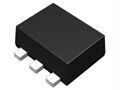
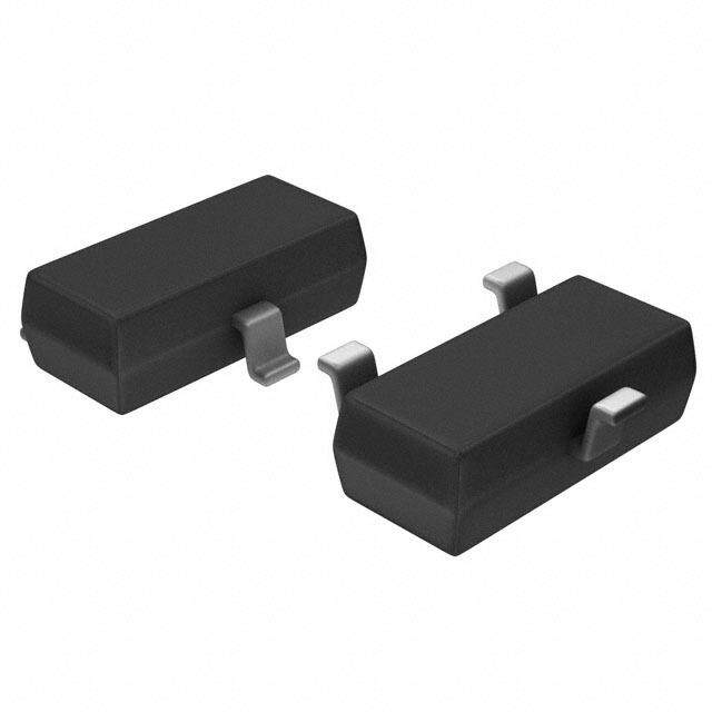
| 产品图片 |
|
| 产品型号 | BU52040HFV-TR |
| rohs | 无铅 / 符合限制有害物质指令(RoHS)规范要求 |
| 产品系列 | - |
| 供应商器件封装 | 5-HVSOF |
| 其它名称 | BU52040HFV-CT |
| 包装 | 剪切带 (CT) |
| 封装/外壳 | SOT-665 |
| 工作温度 | -40°C ~ 85°C |
| 感应范围 | ±3mT |
| 标准包装 | 1 |
| 特性 | - |
| 特色产品 | http://www.digikey.com/cn/zh/ph/rohm/ic.html |
| 电压-电源 | 1.65 V ~ 3.3 V |
| 电流-电源 | 200µA |
| 电流-输出(最大值) | ±0.5mA |
| 类型 | 双极卡锁 |
| 输出类型 | 数字 |


- 商务部:美国ITC正式对集成电路等产品启动337调查
- 曝三星4nm工艺存在良率问题 高通将骁龙8 Gen1或转产台积电
- 太阳诱电将投资9.5亿元在常州建新厂生产MLCC 预计2023年完工
- 英特尔发布欧洲新工厂建设计划 深化IDM 2.0 战略
- 台积电先进制程称霸业界 有大客户加持明年业绩稳了
- 达到5530亿美元!SIA预计今年全球半导体销售额将创下新高
- 英特尔拟将自动驾驶子公司Mobileye上市 估值或超500亿美元
- 三星加码芯片和SET,合并消费电子和移动部门,撤换高东真等 CEO
- 三星电子宣布重大人事变动 还合并消费电子和移动部门
- 海关总署:前11个月进口集成电路产品价值2.52万亿元 增长14.8%


PDF Datasheet 数据手册内容提取
Hall IC Series Bipolar Latch Hall IC BU52040HFV No.10045EBT05 ●Description BU52040 Hall Effect IC for wheel keys / trackballs is designed to detect a switch in magnetic field from N to S (or vice versa) and maintain its detection result on the output until the next switch. Output is pulled low for S-pole fields and high for N-pole fields. This IC is ideal for detecting the number of shaft rotations inside of a wheel key, trackball, or other similar applications. Using two ICs can also enable detection of rotation direction. ●Features 1) Ideally suited for wheel keys or trackballs 2) Micropower operation (small current consumption via intermittent operation method) 3) Ultra-small outline package 4) Supports 1.8 V supply voltage 5) High ESD resistance: 8kV (HBM) ●Applications Wheel keys (zero-contact selection dials), trackballs, and other interface applications. ●Product Lineup Supply current Supply voltage Operation point Hysteresis Period Product name (AVG) Output type Package (V) (mT) (mT) (µs) (µA) BU52040HFV 1.65~3.30 +/-3.0※ 6.0 500 200 CMOS HVSOF5 ※Plus is expressed on the S-pole; minus on the N-pole ●Absolute Maximum Ratings BU52040HFV (Ta = 25°C) Parameters Symbol Limit Unit Power Supply Voltage V -0.1~4.5※1 V DD Output Current I ± 0.5 mA OUT Power dissipation Pd 536※2 mW Operating Temperature Range T -40~+85 °C opr Storage Temperature Range T -40~+125 °C stg ※1. Not to exceed Pd ※2. Reduced by 5.36mW for each increase in Ta of 1℃ over 25℃(mounted on 70mm×70 mm×1.6mm Glass-epoxy PCB) www.rohm.com 1/12 2010.01 - Rev.B © 2010 ROHM Co., Ltd. All rights reserved.
BU52040HFV Technical Note ●Magnetic, Electrical Characteristics BU52040HFV (Unless otherwise specified, V =1.80V, Ta=25°C) DD Limit Parameters Symbol Unit Conditions Min Typ Max Power Supply Voltage V 1.65 1.80 3.30 V DD Operation point B 1.0 3.0 5.0 mT op Release Point B -5.0 -3.0 -1.0 mT rp Hysteresis B - 6.0 - mT hys Period T - 500 1200 µs p B < B ※3 Output High Voltage V V - 0.2 - - V rp OH DD I =-0.5mA OUT B < B※3 Output Low Voltage V - - 0.2 V op OL I =+0.5mA OUT Supply Current 1 I - 200 300 µA V =1.8V, Average DD1(AVG) DD Supply Current V =1.8V, I - 3.0 - mA DD During Startup Time 1 DD1(EN) During Startup Time Value Supply Current V =1.8V, I - 2.0 - µA DD During Standby Time 1 DD1(DIS) During Standby Time Value Supply Current 2 I - 300 450 µA V =2.7V, Average DD2(AVG) DD Supply Current V =2.7V, I - 4.5 - mA DD During Startup Time 2 DD2(EN) During Startup Time Value Supply Current V =2.7V, I - 3.5 - µA DD During Standby Time 2 DD2(DIS) During Standby Time Value ※3. B = Magnetic flux density 1mT=10Gauss Positive (“+”) polarity flux is defined as the magnetic flux from south pole which is direct toward to the branded face of the sensor. After applying power supply, it takes one cycle of period (TP) to become definite output. Radiation hardiness is not designed. www.rohm.com 2/12 2010.01 - Rev.B © 2010 ROHM Co., Ltd. All rights reserved.
BU52040HFV Technical Note ●Figure of measurement circuit B /B op rp T p 200Ω VDD VDD VDD VDD OUT 100μF OUT Oscilloscope GND GND V Bop and Brp are measured with applying the magnetic field The period is monitored by Oscilloscope. from the outside. Fig.1 Bop,Brp measurement circuit Fig.2 Tp measurement circuit V OH VDD VDD 100μF OUT GND V IOUT=0.5mA Fig.3 VOH measurement circuit V OL VDD VDD 100μF OUT GND V I =0.5mA OUT Fig.4 V measurement circuit OL I DD A VDD VDD 2200μF OUT GND Fig.5 I measurement circuit DD www.rohm.com 3/12 2010.01 - Rev.B © 2010 ROHM Co., Ltd. All rights reserved.
BU52040HFV Technical Note ●Reference Data 8.0 8.0 800 ENSITY [mT] 246...000 VDD=1.8V Bop ENSITY [mT] 246...000 Ta = 25°C Bop μs]670000 VDD=1.8V UX D 0.0 Brp UX D 0.0 OD [500 ETIC FL --42..00 ETIC FL --42..00 Brp PERI400 AGN -6.0 AGN -6.0 300 M -8.0-60 -40-20 0 20 40 60 80 100 M -8.01.4 1.8 2.2 2.6 3.0 3.4 3.8 200-60 -40 -20 0 20 40 60 80 100 AMBIENT TEMPERATURE [℃] SUPPLY VOLTAGE [V] AMBIENT TEMPERATURE [℃] Fig.6 Bop,Brp– Fig.7 Bop,Brp– Supply voltage Fig.8 TP– Ambient temperature Ambient temperature 800 A] 400 µA] 400 700 Ta = 25°C ENT [µ 350 VDD=1.8V RENT [ 350 Ta = 25°C μPERIOD [s] 456000000 E SUPPLY CURR 223050000 GE SUPPLY CUR 223050000 300 AG 150 RA 150 ER VE 200 AV 100 A 100 1.4 1.8 2.2 2.6 3.0 3.4 3.8 -60 -40-20 0 20 40 60 80 100 1.4 1.8 2.2 2.6 3.0 3.4 3.8 SUPPLY VOLTAGE [V] AMBIENT TEMPERATURE [℃] SUPPLY VOLTAGE [V] Fig.9 TP– Supply voltage Fig.10 IDD– Ambient temperature Fig.11 IDD – Supply voltage ●Block Diagram BU52040HFV 0.1 µF VDD 4 Adjust the bypass capacitor value as necessary, according to voltage noise conditions, etc. TIMING LOGIC HALL ELEMENT N × DYNAMIC OFFSET NCELLATIO SAMPLE & HOLD LATCH 5 OUT Tde xihrteeec rCtn cMaol OnpnSuel lo-cuutiptop nrue tts otie strhtmoeri nPreaCqls,u weirneitahdb .n leo A C 2 GND Fig.12 5 4 4 5 PIN No. PIN NAME FUNCTION COMMENT 1 N.C. OPEN or Short to GND. 2 GND GROUND 3 N.C. OPEN or Short to GND. 4 VDD POWER SUPPLY 1 2 3 3 2 1 5 OUT OUTPUT Surface Reverse www.rohm.com 4/12 2010.01 - Rev.B © 2010 ROHM Co., Ltd. All rights reserved.
BU52040HFV Technical Note ●Description of Operations (Micro-power Operation) The Hall Effect IC for wheel keys / trackballs adopts an intermittent operation method to save energy. At startup, the Hall elements, amp, comparator and other detection circuits power ON and magnetic detection begins. During standby, the detection circuits power OFF, thereby reducing current consumption. The detection results are held while standby is active, and then output. Reference period: 500 µs (MAX. 1200 µs) Reference startup time: 24 µs I DD Period Startup time Standby t Fig.13 (Offset Cancellation) The Hall elements form an equivalent Wheatstone (resistor) bridge circuit. Offset voltage may be generated by a differential in this bridge resistance, or can arise from changes in resistance due to package or bonding stress. A dynamic offset cancellation circuit is employed to cancel this offset voltage. When Hall elements are connected as shown in Fig. 14 and a magnetic field is applied perpendicularly to the Hall elements, voltage is generated at the mid-point terminal of the bridge. This is known as the Hall voltage. Dynamic cancellation switches the wiring (shown in the figure) to redirect the current flow to a 90˚ angle from its original path, and thereby cancels the Hall voltage. The magnetic signal (only) is maintained in the sample/hold circuit during the offset cancellation process and then released. V DD I B × + Hall Voltage - GND Fig.14 www.rohm.com 5/12 2010.01 - Rev.B © 2010 ROHM Co., Ltd. All rights reserved.
BU52040HFV Technical Note (Magnetic Field Detection Mechanism) OUT [V] High Low B 0 Brp Bop N-pole Magnetic flux density [mT] S-pole Fig.15 The IC detects magnetic fields that running horizontal to the top layer of the package. When the magnetic pole switches from N to S, the output changes from high to low; likewise, when the magnetic pole switches from S to N, the output changes from low to high. The output condition is held unit the next switch in magnetic polarity is detected. [Operation in Continuously Changing Magnetic Fields] Direction of magnet movement S N S N S N Magnet S N S N S N Hall IC S Bop Magnetic field N Brp High Hall IC output Low Fig.16 The IC can detect a continuous switch in magnetic field (from N to S and S to N) as depicted above. www.rohm.com 6/12 2010.01 - Rev.B © 2010 ROHM Co., Ltd. All rights reserved.
BU52040HFV Technical Note ●Intermittent Operation at Power ON VDD Startup time Standby time Startup time Standby time Supply current (Intermittent operation) OUT Indefinite High (N magnetic field present) (B<B ) rp Indefinite interval OUT (S magnetic field present) (B <B) Low op Indefinite interval OUT (No magnetic field present) (Brp<B< Bop) Fig.17 The Hall Effect IC for wheel keys / trackballs adopts an intermittent operation method in detecting the magnetic field during startup, as shown in Fig. 17. It outputs to the appropriate terminal based on the detection result and maintains the output condition during the standby period. The time from power ON until the end of the initial startup period is an indefinite interval, but it cannot exceed the maximum period, 1200μs. To accommodate the system design, the Hall IC output read should be programmed within 1200μs of power ON, but after the time allowed for the period ambient temperature and supply voltage. Additionally, if a magnetic flux density (B) of magnitude greater than B but less than B is applied at power ON, the output rp op from the IC remains undefined and will be either high or low until a flux density exceeding the B or B threshold is applied. op rp ●Application Example Wheel Key Two Hall ICs can enable detection of rotation direction of a magnetic zero-contact wheel key. Circular magnet S N N S S N N S BU52040HFV: 2pcs Mounting Position of Hall IC Inside Wheel Key The angular separation of the two Hall ICs within the footprint of the wheel key depends on N/S division angle of the internal magnet (Φ), and can be set to either Φ/4 or ¾Φ. Mounting the two ICs in this position causes the magnetic phase difference between the ICs to equal ±1/4, and the direction of rotation can be detected by measuring the change in this difference. An example of the magnetic field characteristics for this application is shown in the figure below. 1) Mounting angle of Hall IC = Φ/4 2) Mounting angle of Hall IC = ¾Φ N/S division angle of circular magnet = Φ Φ/4 3/4 Φ Φ Counterclockwise Clockwise rotation N S rotation Hall IC A Hall IC B Hall IC A Hall IC B S N θ θ N S S N N S Center of magnet Center of magnet S N N S N S Mounting Angle of Hall IC Circular Magnet www.rohm.com 7/12 2010.01 - Rev.B © 2010 ROHM Co., Ltd. All rights reserved.
BU52040HFV Technical Note Detection of Rotation Direction 1) Mounting angle = Φ/4 Clockwise Rotation Counterclockwise Rotation Magnetic field applied to IC A Magnetic field applied to IC A Magnetic field applied to IC B Magnetic field applied to IC B Bop Bop S S rotation angle rotation angle N N Brp Brp Ha ll IC A Hall IC A out put output High High Low Low Hall IC B output Hall IC B output High High Low Low Clockwise turn: Output of IC B is low when Counterclockwise turn: Output of IC B is high output of IC A becomes high whenoutputofICAbecomeshigh 2) Mounting angle = ¾Φ Clockwise Rotation Counterclockwise Rotation Magnetic field applied to IC A Magnetic field applied to IC A Magnetic field applied to IC B Magnetic field applied to IC B Bop Bop S S rotation angle rotation angle N N Brp Brp Hall IC A Hall IC A output High output High Low Low Hall IC B Hall IC B output output High High Low Low Clockwise turn: Output of IC B is high when Counterclockwise turn: Output of IC B is a low output of IC A becomes high. when output of IC A becomes high. Because the IC measures changes in magnetic field every 1200 µS, the IC cannot detect changes in rotation at speeds exceeding this period. www.rohm.com 8/12 2010.01 - Rev.B © 2010 ROHM Co., Ltd. All rights reserved.
BU52040HFV Technical Note ●Magnet Selection Horizontally Stacked Magnet Vertically Stacked Magnet S N S N S N S N S S N Flux Flux Because the field loop in horizontally stacked magnets extends for a shorter distance than that of vertically stacked magnets, the gap between the magnet and the hall IC must be decreased. Therefore, if horizontally-stacked magnets are used in the application, the thickness of the magnet or the area of each section should be increased to allow for a larger gap between the magnet and IC. Because the IC is unable to detect rotation direction if using magnets that are smaller than the IC’s package size, ensure that the physical size of each N/S division is larger than the IC’s package, and that the ICs are properly mounted with an angular distance of either Φ/4 or ¾Φ from one another (where Φ = N/S division angle of circular magnet). ●IC Reference Position Mounting angle of Hall IC Magnet N/S division angle = Φ Hall IC (x2) N S Counterclockwise S N Clockwise rotation N S rotation S N N S S N N S N S Circular Magnet ●Position of the Hall Effect IC(Reference) HVSOF5 0.6 0.8 0.2 (UNIT:mm) www.rohm.com 9/12 2010.01 - Rev.B © 2010 ROHM Co., Ltd. All rights reserved.
BU52040HFV Technical Note ●Footprint dimensions (Optimize footprint dimensions to the board design and soldering condition) HVSOF5 (UNIT:mm) ●Terminal Equivalent Circuit Diagram Because they are configured for CMOS (inverter) output, the output pins require no external resistance and allow direct connection to the PC. This, in turn, enables reduction of the current that would otherwise flow to the external resistor during magnetic field detection, and supports overall low current (micropower) operation. OUT VDD GND Fig.18 www.rohm.com 10/12 2010.01 - Rev.B © 2010 ROHM Co., Ltd. All rights reserved.
BU52040HFV Technical Note ●Notes for use 1) Absolute maximum ratings Exceeding the absolute maximum ratings for supply voltage, operating conditions, etc. may result in damage to or destruction of the IC. Because the source (short mode or open mode) cannot be identified if the device is damaged in this way, it is important to take physical safety measures such as fusing when implementing any special mode that operates in excess of absolute rating limits. 2) GND voltage Make sure that the GND terminal potential is maintained at the minimum in any operating state, and is always kept lower than the potential of all other pins. 3) Thermal design Use a thermal design that allows for sufficient margin in light of the power dissipation (Pd) in actual operating conditions. 4) Pin shorts and mounting errors Use caution when positioning the IC for mounting on printed circuit boards. Mounting errors, such as improper positioning or orientation, may damage or destroy the device. The IC may also be damaged or destroyed if output pins are shorted together, or if shorts occur between the output pin and supply pin or GND. 5) Positioning components in proximity to the Hall IC and magnet Positioning magnetic components in close proximity to the Hall IC or magnet may alter the magnetic field, and therefore the magnetic detection operation. Thus, placing magnetic components near the Hall IC and magnet should be avoided in the design if possible. However, where there is no alternative to employing such a design, be sure to thoroughly test and evaluate performance with the magnetic component(s) in place to verify normal operation before implementing the design. 6) Operation in strong electromagnetic fields Exercise extreme caution about using the device in the presence of a strong electromagnetic field, as such use may cause the IC to malfunction. 7) Common impedance Make sure that the power supply and GND wiring limits common impedance to the extent possible by, for example, employing short, thick supply and ground lines. Also, take measures to minimize ripple such as using an inductor or capacitor. 8) GND wiring pattern When both a small-signal GND and high-current GND are provided, single-point grounding at the reference point of the set PCB is recommended, in order to separate the small-signal and high-current patterns, and to ensure that voltage changes due to the wiring resistance and high current do not cause any voltage fluctuation in the small-signal GND. In the same way, care must also be taken to avoid wiring pattern fluctuations in the GND wiring pattern of external components. 9) Power source design Since the IC performs intermittent operation, it has peak current when it’s ON. Please taking that into account and under examine adequate evaluations when designing the power source. www.rohm.com 11/12 2010.01 - Rev.B © 2010 ROHM Co., Ltd. All rights reserved.
BU52040HFV Technical Note ●Ordering part number B U 5 2 0 4 0 H F V - T R Part No Part No Package Packaging and forming specification 52040 HFV : HVSOF5 TR: Embossed tape and reel (HVSOF5) HVSOF5 <Tape and Reel information> 1.6±0.05 (0.8) Tape Embossed carrier tape ±1.60.05 ±1.20.05X 1.28 include BURR)(0.05) 1.150±20.4035 (0.91) (0.41) 34(02.31)5 0.0.2MAX13±0.05 QDofiu rfeaecnettdiiotyn 3T(0RTre0he0elp odcnirs ethcetio lenf tis h tahned 1 apnind oyfo pur opduull cot uist tah1te pt htianep uep opne rt hrieg hritg whth heann ydou hold ) A M ( X S A M 0.6 +0.03–0.02 0.5 0.1 S 0.02 0.22±0.05 0.08M Direction of feed (Unit : mm) Reel ∗ Order quantity needs to be multiple of the minimum quantity. www.rohm.com 12/12 2010.01 - Rev.B © 2010 ROHM Co., Ltd. All rights reserved.
DDaattaasshheeeett Notice Precaution on using ROHM Products 1. Our Products are designed and manufactured for application in ordinary electronic equipments (such as AV equipment, OA equipment, telecommunication equipment, home electronic appliances, amusement equipment, etc.). If you intend to use our Products in devices requiring extremely high reliability (such as medical equipment (Note 1), transport equipment, traffic equipment, aircraft/spacecraft, nuclear power controllers, fuel controllers, car equipment including car accessories, safety devices, etc.) and whose malfunction or failure may cause loss of human life, bodily injury or serious damage to property (“Specific Applications”), please consult with the ROHM sales representative in advance. Unless otherwise agreed in writing by ROHM in advance, ROHM shall not be in any way responsible or liable for any damages, expenses or losses incurred by you or third parties arising from the use of any ROHM’s Products for Specific Applications. (Note1) Medical Equipment Classification of the Specific Applications JAPAN USA EU CHINA CLASSⅢ CLASSⅡb CLASSⅢ CLASSⅢ CLASSⅣ CLASSⅢ 2. ROHM designs and manufactures its Products subject to strict quality control system. However, semiconductor products can fail or malfunction at a certain rate. Please be sure to implement, at your own responsibilities, adequate safety measures including but not limited to fail-safe design against the physical injury, damage to any property, which a failure or malfunction of our Products may cause. The following are examples of safety measures: [a] Installation of protection circuits or other protective devices to improve system safety [b] Installation of redundant circuits to reduce the impact of single or multiple circuit failure 3. Our Products are designed and manufactured for use under standard conditions and not under any special or extraordinary environments or conditions, as exemplified below. Accordingly, ROHM shall not be in any way responsible or liable for any damages, expenses or losses arising from the use of any ROHM’s Products under any special or extraordinary environments or conditions. If you intend to use our Products under any special or extraordinary environments or conditions (as exemplified below), your independent verification and confirmation of product performance, reliability, etc, prior to use, must be necessary: [a] Use of our Products in any types of liquid, including water, oils, chemicals, and organic solvents [b] Use of our Products outdoors or in places where the Products are exposed to direct sunlight or dust [c] Use of our Products in places where the Products are exposed to sea wind or corrosive gases, including Cl2, H2S, NH3, SO2, and NO2 [d] Use of our Products in places where the Products are exposed to static electricity or electromagnetic waves [e] Use of our Products in proximity to heat-producing components, plastic cords, or other flammable items [f] Sealing or coating our Products with resin or other coating materials [g] Use of our Products without cleaning residue of flux (even if you use no-clean type fluxes, cleaning residue of flux is recommended); or Washing our Products by using water or water-soluble cleaning agents for cleaning residue after soldering [h] Use of the Products in places subject to dew condensation 4. The Products are not subject to radiation-proof design. 5. Please verify and confirm characteristics of the final or mounted products in using the Products. 6. In particular, if a transient load (a large amount of load applied in a short period of time, such as pulse. is applied, confirmation of performance characteristics after on-board mounting is strongly recommended. Avoid applying power exceeding normal rated power; exceeding the power rating under steady-state loading condition may negatively affect product performance and reliability. 7. De-rate Power Dissipation (Pd) depending on Ambient temperature (Ta). When used in sealed area, confirm the actual ambient temperature. 8. Confirm that operation temperature is within the specified range described in the product specification. 9. ROHM shall not be in any way responsible or liable for failure induced under deviant condition from what is defined in this document. Precaution for Mounting / Circuit board design 1. When a highly active halogenous (chlorine, bromine, etc.) flux is used, the residue of flux may negatively affect product performance and reliability. 2. In principle, the reflow soldering method must be used; if flow soldering method is preferred, please consult with the ROHM representative in advance. For details, please refer to ROHM Mounting specification Notice - GE Rev.002 © 2014 ROHM Co., Ltd. All rights reserved.
DDaattaasshheeeett Precautions Regarding Application Examples and External Circuits 1. If change is made to the constant of an external circuit, please allow a sufficient margin considering variations of the characteristics of the Products and external components, including transient characteristics, as well as static characteristics. 2. You agree that application notes, reference designs, and associated data and information contained in this document are presented only as guidance for Products use. Therefore, in case you use such information, you are solely responsible for it and you must exercise your own independent verification and judgment in the use of such information contained in this document. ROHM shall not be in any way responsible or liable for any damages, expenses or losses incurred by you or third parties arising from the use of such information. Precaution for Electrostatic This Product is electrostatic sensitive product, which may be damaged due to electrostatic discharge. Please take proper caution in your manufacturing process and storage so that voltage exceeding the Products maximum rating will not be applied to Products. Please take special care under dry condition (e.g. Grounding of human body / equipment / solder iron, isolation from charged objects, setting of Ionizer, friction prevention and temperature / humidity control). Precaution for Storage / Transportation 1. Product performance and soldered connections may deteriorate if the Products are stored in the places where: [a] the Products are exposed to sea winds or corrosive gases, including Cl2, H2S, NH3, SO2, and NO2 [b] the temperature or humidity exceeds those recommended by ROHM [c] the Products are exposed to direct sunshine or condensation [d] the Products are exposed to high Electrostatic 2. Even under ROHM recommended storage condition, solderability of products out of recommended storage time period may be degraded. It is strongly recommended to confirm solderability before using Products of which storage time is exceeding the recommended storage time period. 3. Store / transport cartons in the correct direction, which is indicated on a carton with a symbol. Otherwise bent leads may occur due to excessive stress applied when dropping of a carton. 4. Use Products within the specified time after opening a humidity barrier bag. Baking is required before using Products of which storage time is exceeding the recommended storage time period. Precaution for Product Label QR code printed on ROHM Products label is for ROHM’s internal use only. Precaution for Disposition When disposing Products please dispose them properly using an authorized industry waste company. Precaution for Foreign Exchange and Foreign Trade act Since our Products might fall under controlled goods prescribed by the applicable foreign exchange and foreign trade act, please consult with ROHM representative in case of export. Precaution Regarding Intellectual Property Rights 1. All information and data including but not limited to application example contained in this document is for reference only. ROHM does not warrant that foregoing information or data will not infringe any intellectual property rights or any other rights of any third party regarding such information or data. ROHM shall not be in any way responsible or liable for infringement of any intellectual property rights or other damages arising from use of such information or data.: 2. No license, expressly or implied, is granted hereby under any intellectual property rights or other rights of ROHM or any third parties with respect to the information contained in this document. Other Precaution 1. This document may not be reprinted or reproduced, in whole or in part, without prior written consent of ROHM. 2. The Products may not be disassembled, converted, modified, reproduced or otherwise changed without prior written consent of ROHM. 3. In no event shall you use in any way whatsoever the Products and the related technical information contained in the Products or this document for any military purposes, including but not limited to, the development of mass-destruction weapons. 4. The proper names of companies or products described in this document are trademarks or registered trademarks of ROHM, its affiliated companies or third parties. Notice - GE Rev.002 © 2014 ROHM Co., Ltd. All rights reserved.
DDaattaasshheeeett General Precaution 1. Before you use our Products, you are requested to carefully read this document and fully understand its contents. ROHM shall not be in any way responsible or liable for failure, malfunction or accident arising from the use of a ny ROHM’s Products against warning, caution or note contained in this document. 2. All information contained in this document is current as of the issuing date and subj ect to change without any prior notice. Before purchasing or using ROHM’s Products, please confirm the latest information with a ROHM sale s representative. 3. The information contained in this document is provided on an “as is” basis and ROHM does not warrant that all information contained in this document is accurate an d/or error-free. ROHM shall not be in any way responsible or liable for any damages, expenses or losses incurred by you or third parties resulting from inaccuracy or errors of or concerning such information. Notice – WE Rev.001 © 2014 ROHM Co., Ltd. All rights reserved.
Mouser Electronics Authorized Distributor Click to View Pricing, Inventory, Delivery & Lifecycle Information: R OHM Semiconductor: BU52040HFV-TR