ICGOO在线商城 > 传感器,变送器 > 磁性传感器 - 开关(固态) > BU52011HFV-TR
 Datasheet下载
- 型号: BU52011HFV-TR
- 制造商: ROHM Semiconductor
- 库位|库存: xxxx|xxxx
- 要求:
| 数量阶梯 | 香港交货 | 国内含税 |
| +xxxx | $xxxx | ¥xxxx |
查看当月历史价格
查看今年历史价格
BU52011HFV-TR产品简介:
ICGOO电子元器件商城为您提供BU52011HFV-TR由ROHM Semiconductor设计生产,在icgoo商城现货销售,并且可以通过原厂、代理商等渠道进行代购。 BU52011HFV-TR价格参考¥0.45-¥0.56。ROHM SemiconductorBU52011HFV-TR封装/规格:磁性传感器 - 开关(固态), Digital Switch Omnipolar Switch Push-Pull Hall Effect HVSOF5。您可以下载BU52011HFV-TR参考资料、Datasheet数据手册功能说明书,资料中有BU52011HFV-TR 详细功能的应用电路图电压和使用方法及教程。
BU52011HFV-TR 是由罗姆半导体(Rohm Semiconductor)生产的一款磁性传感器,属于固态开关型霍尔效应传感器。它主要用于检测磁场的存在与否,并据此实现开关功能,广泛应用于以下场景:

1. 工业自动化设备:用于位置检测、接近检测和速度测量等,如气缸位置检测、机械臂动作确认等。
2. 家电产品:例如洗衣机、冰箱中用于检测门是否关闭、转子位置检测等,提高设备的安全性和可靠性。
3. 汽车电子系统:用于无刷直流电机的转子位置检测、车门/后备箱开闭状态检测、座椅位置调节控制等。
4. 消费类电子产品:如智能手机、平板电脑中的翻盖检测、手写笔存在检测等功能。
5. 安防系统:用于门窗磁控开关,检测门窗是否开启或关闭。

该器件采用高灵敏度霍尔元件与CMOS技术结合,具有低功耗、高响应速度、抗干扰能力强等特点,适合在各种复杂环境中稳定工作。其小型化封装也便于集成到空间受限的设计中。
| 参数 | 数值 |
| 产品目录 | |
| 描述 | IC HALL EFFECT SW BIPO HVSOF5工业霍耳效应/磁性传感器 ULTRA SMALL DETECT SENSOR; 1.65-3.3V |
| 产品分类 | 磁性传感器 - 霍尔效应,数字开关,线性,罗盘 (IC)磁性传感器 |
| 品牌 | Rohm Semiconductor |
| 产品手册 | |
| 产品图片 |
|
| rohs | 符合RoHS无铅 / 符合限制有害物质指令(RoHS)规范要求 |
| 产品系列 | 工业霍耳效应/磁性传感器,ROHM Semiconductor BU52011HFV-TR- |
| 数据手册 | |
| 产品型号 | BU52011HFV-TR |
| 产品种类 | 工业霍耳效应/磁性传感器 |
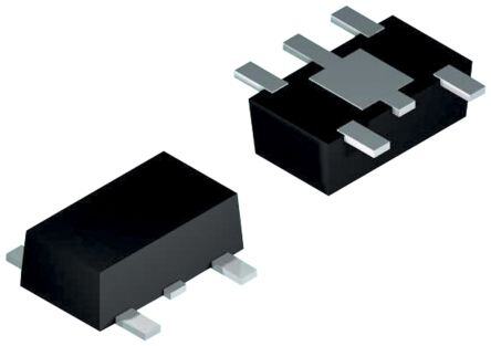
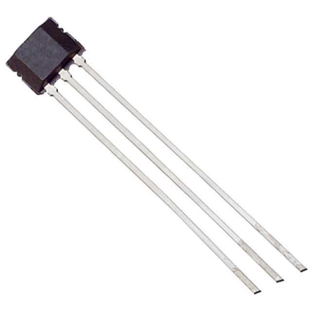
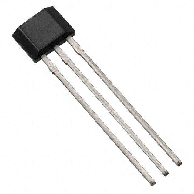
| 供应商器件封装 | 5-HVSOF |
| 其它名称 | BU52011HFV-TR-ND |
| 包装 | 带卷 (TR) |
| 商标 | ROHM Semiconductor |
| 安装风格 | SMD/SMT |
| 封装 | Reel |
| 封装/外壳 | SOT-665 |
| 封装/箱体 | HVSOF |
| 工作温度 | -40°C ~ 85°C |
| 工作点最小值/最大值 | - 5 mT to 5 mT |
| 工作电源电压 | 1.8 V or 2.5 V |
| 工厂包装数量 | 3000 |
| 感应范围 | ±3mT 跳闸, ±2.1mT 释放 |
| 操作类型 | Bipolar |
| 最大工作温度 | + 85 C |
| 最大输出电流 | 0.5 mA |
| 最小工作温度 | - 40 C |
| 标准包装 | 3,000 |
| 特性 | - |
| 特色产品 | http://www.digikey.com/cn/zh/ph/rohm/ic.html |
| 电压-电源 | 1.65 V ~ 3.3 V |
| 电流-电源 | 8µA |
| 电流-输出(最大值) | ±0.5mA |
| 电流额定值 | 5 uA |
| 类型 | 全极开关 |
| 输出类型 | 数字 |


- 商务部:美国ITC正式对集成电路等产品启动337调查
- 曝三星4nm工艺存在良率问题 高通将骁龙8 Gen1或转产台积电
- 太阳诱电将投资9.5亿元在常州建新厂生产MLCC 预计2023年完工
- 英特尔发布欧洲新工厂建设计划 深化IDM 2.0 战略
- 台积电先进制程称霸业界 有大客户加持明年业绩稳了
- 达到5530亿美元!SIA预计今年全球半导体销售额将创下新高
- 英特尔拟将自动驾驶子公司Mobileye上市 估值或超500亿美元
- 三星加码芯片和SET,合并消费电子和移动部门,撤换高东真等 CEO
- 三星电子宣布重大人事变动 还合并消费电子和移动部门
- 海关总署:前11个月进口集成电路产品价值2.52万亿元 增长14.8%


PDF Datasheet 数据手册内容提取
Hall ICs Omnipolar Detection Hall ICs BU52001GUL,BU52011HFV,BU52021HFV,BU52015GUL,BU52025G,BU52053NVX, BU52054GWZ,BU52055GWZ,BU52056NVX,BU52061NVX,BD7411G No.10045EGT02 ●Description The omnipolar Hall ICs are magnetic switches that can operate both S-and N-pole, upon which the output goes from Hi to Low. In addition to regular single-output Hall ICs, We offer a lineup of dual-output units with a reverse output terminal (active High). ●Features 1) Omnipolar detection 2) Micro power operation (small current using intermittent operation method)(BD7411G is excluded.) 3) Ultra-compact and thin wafer level CSP4 package (BU52054GWZ, BU52055GWZ) 4) Ultra-compact wafer level CSP4 package (BU52015GUL, BU52001GUL) 5) Ultra-Small outline package SSON004X1216 (BU52061NVX, BU52053NVX, BU52056NVX) 6) Ultra-Small outline package HVSOF5 (BU52011HFV, BU52021HFV) 7) Small outline package (BU52025G, BD7411G) 8) Line up of supply voltage For 1.8V Power supply voltage (BU52054GWZ, BU52055GWZ, BU52015GUL, BU52061NVX, BU52053NVX, BU52056NVX, BU52011HFV) For 3.0V Power supply voltage (BU52001GUL) For 3.3V Power supply voltage (BU52021HFV, BU52025G) For 5.0V Power supply voltage (BD7411G) 9) Dual output type (BU52015GUL) 10) High ESD resistance 8kV (HBM) (6kV for BU52056NVX) ●Applications Mobile phones, notebook computers, digital video camera, digital still camera, white goods etc. ●Lineup matrix Supply Operate Supply current Output Hysteresis Period Package Product name voltage point (AVG) type (V) (mT) (mT) (ms) (A) BU52054GWZ 1.65~3.60 +/-6.3 ※ 0.9 50 5.0µ CMOS UCSP35L1 BU52055GWZ 1.65~3.60 +/-4.1 ※ 0.8 50 5.0µ CMOS UCSP35L1 BU52015GUL 1.65~3.30 +/-3.0 ※ 0.9 50 5.0µ CMOS VCSP50L1 BU52001GUL 2.40~3.30 +/-3.7 ※ 0.8 50 8.0µ CMOS VCSP50L1 BU52061NVX 1.65~3.60 +/-3.3 ※ 0.9 50 4.0µ CMOS SSON004X1216 BU52053NVX 1.65~3.60 +/-3.0 ※ 0.9 50 5.0µ CMOS SSON004X1216 BU52056NVX 1.65~3.60 +/-4.6 ※ 0.8 50 5.0µ CMOS SSON004X1216 BU52011HFV 1.65~3.30 +/-3.0 ※ 0.9 50 5.0µ CMOS HVSOF5 BU52021HFV 2.40~3.60 +/-3.7 ※ 0.8 50 8.0µ CMOS HVSOF5 BU52025G 2.40~3.60 +/-3.7 ※ 0.8 50 8.0µ CMOS SSOP5 BD7411G 4.50~5.50 +/-3.4 ※ 0.4 - 2.0m CMOS SSOP5 ※Plus is expressed on the S-pole; minus on the N-pole www.rohm.com 1/31 2011.12 - Rev.G © 2011 ROHM Co., Ltd. All rights reserved.
BU52001GUL,BU52011HFV,BU52021HFV,BU52015GUL,BU52025G,BU52053NVX, BU52054GWZ,BU52055GWZ,BU52056NVX,BU52061NVX,BD7411G Technical Note ●Absolute maximum ratings BU52054GWZ, BU52055GWZ (Ta=25℃) BU52015GUL (Ta=25℃) Parameter Symbol Ratings Unit Parameter Symbol Ratings Unit Power Supply Voltage V -0.1~+4.5※1 V Power Supply Voltage V -0.1~+4.5※3 V DD DD Output Current I ±0.5 mA Output Current I ±0.5 mA OUT OUT Power Dissipation Pd 100※2 mW Power Dissipation Pd 420※4 mW Operating Operating T -40~+85 ℃ T -40~+85 ℃ Temperature Range opr Temperature Range opr Storage Storage T -40~+125 ℃ T -40~+125 ℃ Temperature Range stg Temperature Range stg ※1. Not to exceed Pd ※3. Not to exceed Pd ※2. Reduced by 1.00mW for each increase in Ta of 1℃ over 25℃ ※4. Reduced by 4.20mW for each increase in Ta of 1℃ over 25℃ (mounted on 24mm×20mm Glass-epoxy PCB) (mounted on 50mm×58mm Glass-epoxy PCB) BU52001GUL (Ta=25℃) BU52061NVX, BU52053NVX, BU52056NVX(Ta=25℃) Parameter Symbol Ratings Unit Parameter Symbol Ratings Unit Power Supply Voltage V -0.1~+4.5※5 V Power Supply Voltage V -0.1~+4.5※7 V DD DD Output Current I ±1 mA Output Current I ±0.5 mA OUT OUT Power Dissipation Pd 420※6 mW Power Dissipation Pd 2049※8 mW Operating Operating T -40~+85 ℃ T -40~+85 ℃ Temperature Range opr Temperature Range opr Storage Storage T -40~+125 ℃ T -40~+125 ℃ Temperature Range stg Temperature Range stg ※5. Not to exceed Pd ※7. Not to exceed Pd ※6. Reduced by 4.20mW for each increase in Ta of 1℃ over 25℃ ※8. Reduced by 4.20mW for each increase in Ta of 1℃ over 25℃ (mounted on 50mm×58mm Glass-epoxy PCB) (mounted on 50mm×58mm Glass-epoxy PCB) BU52011HFV (Ta=25℃) BU52021HFV (Ta=25℃) Parameter Symbol Ratings Unit Parameter Symbol Ratings Unit Power Supply Voltage V -0.1~+4.5※9 V Power Supply Voltage V -0.1~+4.5※11 V DD DD Output Current I ±0.5 mA Output Current I ±1 mA OUT OUT Power Dissipation Pd 536※10 mW Power Dissipation Pd 536※12 mW Operating Operating T -40~+85 ℃ T -40~+85 ℃ Temperature Range opr Temperature Range opr Storage Storage T -40~+125 ℃ T -40~+125 ℃ Temperature Range stg Temperature Range stg ※9. Not to exceed Pd ※11 Not to exceed Pd ※10. Reduced by5.36mW for each increase in Ta of 1℃ over 25℃ ※12. Reduced by 5.36mW for each increase in Ta of 1℃ over 25℃ (mounted on 70mm×70 mm×1.6mm Glass-epoxy PCB) (mounted on 70mm×70 mm×1.6mm Glass-epoxy PCB) BU52025G (Ta=25℃) BD7411G (Ta=25℃) Parameter Symbol Ratings Unit Parameter Symbol Ratings Unit Power Supply Voltage V -0.1~+4.5※13 V Power Supply Voltage V -0.3~+7.0※15 V DD DD Output Current I ±1 mA Output Current I ±1 mA OUT OUT Power Dissipation Pd 540※14 mW Power Dissipation Pd 540※16 mW Operating Operating T -40~+85 ℃ T -40~+85 ℃ Temperature Range opr Temperature Range opr Storage Storage T -40~+125 ℃ T -55~+150 ℃ Temperature Range stg Temperature Range stg ※13. Not to exceed Pd ※15. Not to exceed Pd ※14. Reduced by 5.40mW for each increase in Ta of 1℃ over 25℃ ※16. Reduced by 5.40mW for each increase in Ta of 1℃ over 25℃ (mounted on 70mm×70 mm×1.6mm Glass-epoxy PCB) (mounted on 70mm×70 mm×1.6mm Glass-epoxy PCB) www.rohm.com 2/31 2011.12 - Rev.G © 2011 ROHM Co., Ltd. All rights reserved.
BU52001GUL,BU52011HFV,BU52021HFV,BU52015GUL,BU52025G,BU52053NVX, BU52054GWZ,BU52055GWZ,BU52056NVX,BU52061NVX,BD7411G Technical Note ●Magnetic, Electrical characteristics BU52054GWZ (Unless otherwise specified, V =1.80V, Ta=25℃) DD Limits Parameter Symbol Unit Conditions Min. Typ. Max. Power Supply Voltage V 1.65 1.80 3.60 V DD B - 6.3 7.9 opS Operate Point mT B -7.9 -6.3 - opN B 3.5 5.4 - rpS Release Point mT B - -5.4 -3.5 rpN B - 0.9 - hysS Hysteresis mT B - 0.9 - hysN Period T - 50 100 ms p B <B<B ※17 Output High Voltage V V -0.2 - - V rpN rpS OH DD I =-0.5mA OUT B<B , B <B ※17 Output Low Voltage V - - 0.2 V opN opS OL I =+0.5mA OUT Supply Current I - 5 8 µA Average DD(AVG) Supply Current During Startup Time I - 2.8 - mA During Startup Time Value DD(EN) Supply Current During Standby Time I - 1.8 - µA During Standby Time Value DD(DIS) ※17 B = Magnetic flux density 1mT=10Gauss Positive (“+”) polarity flux is defined as the magnetic flux from south pole which is direct toward to the branded face of the sensor. After applying power supply, it takes one cycle of period (T) to become definite output. P Radiation hardiness is not designed. www.rohm.com 3/31 2011.12 - Rev.G © 2011 ROHM Co., Ltd. All rights reserved.
BU52001GUL,BU52011HFV,BU52021HFV,BU52015GUL,BU52025G,BU52053NVX, BU52054GWZ,BU52055GWZ,BU52056NVX,BU52061NVX,BD7411G Technical Note BU52055GWZ (Unless otherwise specified, V =1.80V, Ta=25℃) DD Limits Parameter Symbol Unit Conditions Min. Typ. Max. Power Supply Voltage V 1.65 1.80 3.60 V DD B - 4.1 5.5 opS Operate Point mT B -5.5 -4.1 - opN B 1.5 3.3 - rpS Release Point mT B - -3.3 -1.5 rpN B - 0.8 - hysS Hysteresis mT B - 0.8 - hysN Period T - 50 100 ms p B <B<B ※18 Output High Voltage V V -0.2 - - V rpN rpS OH DD I =-0.5mA OUT B<B , B <B ※18 Output Low Voltage V - - 0.2 V opN opS OL I =+0.5mA OUT Supply Current I - 5 8 µA Average DD(AVG) Supply Current During Startup Time I - 2.8 - mA During Startup Time Value DD(EN) Supply Current During Standby Time I - 1.8 - µA During Standby Time Value DD(DIS) ※18 B = Magnetic flux density 1mT=10Gauss Positive (“+”) polarity flux is defined as the magnetic flux from south pole which is direct toward to the branded face of the sensor. After applying power supply, it takes one cycle of period (T) to become definite output. P Radiation hardiness is not designed. www.rohm.com 4/31 2011.12 - Rev.G © 2011 ROHM Co., Ltd. All rights reserved.
BU52001GUL,BU52011HFV,BU52021HFV,BU52015GUL,BU52025G,BU52053NVX, BU52054GWZ,BU52055GWZ,BU52056NVX,BU52061NVX,BD7411G Technical Note BU52015GUL (Unless otherwise specified, V =1.80V, Ta=25℃) DD Limits Parameter Symbol Unit Conditions Min. Typ. Max. Power Supply Voltage V 1.65 1.80 3.30 V DD B - 3.0 5.0 opS Operate Point mT B -5.0 -3.0 - opN B 0.6 2.1 - rpS Release Point mT B - -2.1 -0.6 rpN B - 0.9 - hysS Hysteresis mT B - 0.9 - hysN Period T - 50 100 ms p OUT1: B <B<B ※19 rpN rpS Output High Voltage V V -0.2 - - V OUT2: B<B , B <B OH DD opN opS I = -0.5mA OUT OUT1: B<B , B <B ※19 opN opS Output Low Voltage V - - 0.2 V OUT2: B <B<B OL rpN rpS I = +0.5mA OUT Supply Current 1 I - 5 8 µA V =1.8V, Average DD1(AVG) DD V =1.8V, Supply Current During Startup Time 1 I - 2.8 - mA DD DD1(EN) During Startup Time Value V =1.8V, Supply Current During Standby Time 1 I - 1.8 - µA DD DD1(DIS) During Standby Time Value Supply Current 2 I - 8 12 µA V =2.7V, Average DD2(AVG) DD V =2.7V, Supply Current During Startup Time 2 I - 4.5 - mA DD DD2(EN) During Startup Time Value V =2.7V, Supply Current During Standby Time 2 I - 4.0 - µA DD DD2(DIS) During Standby Time Value ※19 B = Magnetic flux density 1mT=10Gauss Positive (“+”) polarity flux is defined as the magnetic flux from south pole which is direct toward to the branded face of the sensor. After applying power supply, it takes one cycle of period (T) to become definite output. P Radiation hardiness is not designed. www.rohm.com 5/31 2011.12 - Rev.G © 2011 ROHM Co., Ltd. All rights reserved.
BU52001GUL,BU52011HFV,BU52021HFV,BU52015GUL,BU52025G,BU52053NVX, BU52054GWZ,BU52055GWZ,BU52056NVX,BU52061NVX,BD7411G Technical Note BU52001GUL (Unless otherwise specified, V =3.0V, Ta=25℃) DD Limits Parameter Symbol Unit Conditions Min. Typ. Max. Power Supply Voltage V 2.4 3.0 3.3 V DD B - 3.7 5.5 opS Operate Point mT B -5.5 -3.7 - opN B 0.8 2.9 - rpS Release Point mT B - -2.9 -0.8 rpN B - 0.8 - hysS Hysteresis mT B - 0.8 - hysN Period T - 50 100 ms p B <B<B ※20 Output High Voltage V V -0.4 - - V rpN rpS OH DD I =-1.0mA OUT B<B ,B <B ※20 Output Low Voltage V - - 0.4 V opN opS OL I =+1.0mA OUT Supply Current I - 8 12 µA Average DD(AVG) Supply Current During Startup Time I - 4.7 - mA During Startup Time Value DD(EN) Supply Current During Standby Time I - 3.8 - µA During Standby Time Value DD(DIS) ※20 B = Magnetic flux density 1mT=10Gauss Positive (“+”) polarity flux is defined as the magnetic flux from south pole which is direct toward to the branded face of the sensor. After applying power supply, it takes one cycle of period (T) to become definite output. P Radiation hardiness is not designed. www.rohm.com 6/31 2011.12 - Rev.G © 2011 ROHM Co., Ltd. All rights reserved.
BU52001GUL,BU52011HFV,BU52021HFV,BU52015GUL,BU52025G,BU52053NVX, BU52054GWZ,BU52055GWZ,BU52056NVX,BU52061NVX,BD7411G Technical Note BU52061NVX (Unless otherwise specified, V =1.80V, Ta=25℃) DD Limits Parameter Symbol Unit Conditions Min. Typ. Max. Power Supply Voltage V 1.65 1.80 3.60 V DD B 2.3 3.3 4.7 opS Operate Point mT B -4.7 -3.3 -2.3 opN B 1.2 2.4 3.4 rpS Release Point mT B -3.4 -2.4 -1.2 rpN B - 0.9 - hysS Hysteresis mT B - 0.9 - hysN Period T - 50 100 ms p B <B<B ※21 Output High Voltage V V -0.2 - - V rpN rpS OH DD I =-0.5mA OUT B<B , B <B ※21 Output Low Voltage V - - 0.2 V opN opS OL I =+0.5mA OUT Supply Current 1 I - 4 7 µA VDD=1.8V, Average DD1(AVG) V =1.8V, Supply Current During Startup Time 1 I - 5.0 - mA DD DD1(EN) During Startup Time Value V =1.8V, Supply Current During Standby Time 1 I - 1.8 - µA DD DD1(DIS) During Standby Time Value Supply Current 2 I - 9 16 µA V =3.0V, Average DD2(AVG) DD V =3.0V, Supply Current During Startup Time 2 I - 9.0 - mA DD DD2(EN) During Startup Time Value V =3.0V, Supply Current During Standby Time 2 I - 4.4 - µA DD DD2(DIS) During Standby Time Value ※21 B = Magnetic flux density 1mT=10Gauss Positive (“+”) polarity flux is defined as the magnetic flux from south pole which is direct toward to the branded face of the sensor. After applying power supply, it takes one cycle of period (T) to become definite output. P Radiation hardiness is not designed. www.rohm.com 7/31 2011.12 - Rev.G © 2011 ROHM Co., Ltd. All rights reserved.
BU52001GUL,BU52011HFV,BU52021HFV,BU52015GUL,BU52025G,BU52053NVX, BU52054GWZ,BU52055GWZ,BU52056NVX,BU52061NVX,BD7411G Technical Note BU52053NVX (Unless otherwise specified, V =1.80V, Ta=25℃) DD Limits Parameter Symbol Unit Conditions Min. Typ. Max. Power Supply Voltage V 1.65 1.80 3.60 V DD B - 3.0 5.0 opS Operate Point mT B -5.0 -3.0 - opN B 0.6 2.1 - rpS Release Point mT B - -2.1 -0.6 rpN B - 0.9 - hysS Hysteresis mT B - 0.9 - hysN Period T - 50 100 ms p B <B<B ※22 Output High Voltage V V -0.2 - - V rpN rpS OH DD I =-0.5mA OUT B<B , B <B ※22 Output Low Voltage V - - 0.2 V opN opS OL I =+0.5mA OUT Supply Current I - 5 8 µA Average DD(AVG) Supply Current During Startup Time I - 2.8 - mA During Startup Time Value DD(EN) Supply Current During Standby Time I - 1.8 - µA During Standby Time Value DD(DIS) ※22 B = Magnetic flux density 1mT=10Gauss Positive (“+”) polarity flux is defined as the magnetic flux from south pole which is direct toward to the branded face of the sensor. After applying power supply, it takes one cycle of period (T) to become definite output. P Radiation hardiness is not designed. www.rohm.com 8/31 2011.12 - Rev.G © 2011 ROHM Co., Ltd. All rights reserved.
BU52001GUL,BU52011HFV,BU52021HFV,BU52015GUL,BU52025G,BU52053NVX, BU52054GWZ,BU52055GWZ,BU52056NVX,BU52061NVX,BD7411G Technical Note BU52011HFV (Unless otherwise specified, V =1.80V, Ta=25℃) DD Limits Parameter Symbol Unit Conditions Min. Typ. Max. Power Supply Voltage V 1.65 1.80 3.30 V DD B - 3.0 5.0 opS Operate Point mT B -5.0 -3.0 - opN B 0.6 2.1 - rpS Release Point mT B - -2.1 -0.6 rpN B - 0.9 - hysS Hysteresis mT B - 0.9 - hysN Period T - 50 100 ms p B <B<B ※23 Output High Voltage V V -0.2 - - V rpN rpS OH DD I =-0.5mA OUT B<B , B <B ※23 Output Low Voltage V - - 0.2 V opN opS OL I =+0.5mA OUT Supply Current 1 I - 5 8 µA V =1.8V, Average DD1(AVG) DD V =1.8V, Supply Current During Startup Time 1 I - 2.8 - mA DD DD1(EN) During Startup Time Value V =1.8V, Supply Current During Standby Time 1 I - 1.8 - µA DD DD1(DIS) During Standby Time Value Supply Current 2 I - 8 12 µA V =2.7V, Average DD2(AVG) DD V =2.7V, Supply Current During Startup Time 2 I - 4.5 - mA DD DD2(EN) During Startup Time Value V =2.7V, Supply Current During Standby Time 2 I - 4.0 - µA DD DD2(DIS) During Standby Time Value ※23 B = Magnetic flux density 1mT=10Gauss Positive (“+”) polarity flux is defined as the magnetic flux from south pole which is direct toward to the branded face of the sensor. After applying power supply, it takes one cycle of period (T) to become definite output. P Radiation hardiness is not designed. www.rohm.com 9/31 2011.12 - Rev.G © 2011 ROHM Co., Ltd. All rights reserved.
BU52001GUL,BU52011HFV,BU52021HFV,BU52015GUL,BU52025G,BU52053NVX, BU52054GWZ,BU52055GWZ,BU52056NVX,BU52061NVX,BD7411G Technical Note BU52056NVX (Unless otherwise specified, V =1.80V, Ta=25℃) DD Limits Parameter Symbol Unit Conditions Min. Typ. Max. Power Supply Voltage V 1.65 1.80 3.60 V DD B - 4.6 6.4 opS Operate Point mT B -6.4 -4.6 - opN B 2.0 3.8 - rpS Release Point mT B - -3.8 -2.0 rpN B - 0.8 - hysS Hysteresis mT B - 0.8 - hysN Period T - 50 100 ms p B <B<B ※24 Output High Voltage V V -0.2 - - V rpN rpS OH DD I =-0.5mA OUT B<B , B <B ※24 Output Low Voltage V - - 0.2 V opN opS OL I =+0.5mA OUT Supply Current I - 5 8 µA Average DD(AVG) Supply Current During Startup Time I - 2.8 - mA During Startup Time Value DD(EN) Supply Current During Standby Time I - 1.8 - µA During Standby Time Value DD(DIS) ※24 B = Magnetic flux density 1mT=10Gauss Positive (“+”) polarity flux is defined as the magnetic flux from south pole which is direct toward to the branded face of the sensor. After applying power supply, it takes one cycle of period (T) to become definite output. P Radiation hardiness is not designed. www.rohm.com 10/31 2011.12 - Rev.G © 2011 ROHM Co., Ltd. All rights reserved.
BU52001GUL,BU52011HFV,BU52021HFV,BU52015GUL,BU52025G,BU52053NVX, BU52054GWZ,BU52055GWZ,BU52056NVX,BU52061NVX,BD7411G Technical Note BU52021HFV,BU52025G (Unless otherwise specified, V =3.0V, Ta=25℃) DD Limits Parameter Symbol Unit Conditions Min. Typ. Max. Power Supply Voltage V 2.4 3.0 3.6 V DD B - 3.7 5.5 opS Operate Point mT B -5.5 -3.7 - opN B 0.8 2.9 - rpS Release Point mT B - -2.9 -0.8 rpN B - 0.8 - hysS Hysteresis mT B - 0.8 - hysN Period T - 50 100 ms p B <B<B ※25 Output High Voltage V V -0.4 - - V rpN rpS OH DD I =-1.0mA OUT B<B , B <B ※25 Output Low Voltage V - - 0.4 V opN opS OL I =+1.0mA OUT Supply Current I - 8 12 µA Average DD(AVG) Supply Current During Startup Time I - 4.7 - mA During Startup Time Value DD(EN) Supply Current During Standby Time I - 3.8 - µA During Standby Time Value DD(DIS) ※25 B = Magnetic flux density 1mT=10Gauss Positive (“+”) polarity flux is defined as the magnetic flux from south pole which is direct toward to the branded face of the sensor. After applying power supply, it takes one cycle of period (T) to become definite output. P Radiation hardiness is not designed. www.rohm.com 11/31 2011.12 - Rev.G © 2011 ROHM Co., Ltd. All rights reserved.
BU52001GUL,BU52011HFV,BU52021HFV,BU52015GUL,BU52025G,BU52053NVX, BU52054GWZ,BU52055GWZ,BU52056NVX,BU52061NVX,BD7411G Technical Note BD7411G (Unless otherwise specified, V =5.0V, Ta=25℃) DD Limits Parameter Symbol Unit Conditions Min. Typ. Max. Power Supply Voltage V 4.5 5.0 5.5 V DD B - 3.4 5.6 opS Operate Point mT B -5.6 -3.4 - opN B 1.5 3.0 - rpS Release Point mT B - -3.0 -1.5 rpN B - 0.4 - hysS Hysteresis mT B - 0.4 - hysN B <B<B ※26 Output High Voltage V 4.6 - - V rpN rpS OH I =-1.0mA OUT B<B , B <B ※26 Output Low Voltage V - - 0.4 V opN opS OL I =+1.0mA OUT Supply Current I - 2 4 mA DD ※26 B = Magnetic flux density 1mT=10Gauss Positive (“+”) polarity flux is defined as the magnetic flux from south pole which is direct toward to the branded face of the sensor. Radiation hardiness is not designed. www.rohm.com 12/31 2011.12 - Rev.G © 2011 ROHM Co., Ltd. All rights reserved.
BU52001GUL,BU52011HFV,BU52021HFV,BU52015GUL,BU52025G,BU52053NVX, BU52054GWZ,BU52055GWZ,BU52056NVX,BU52061NVX,BD7411G Technical Note ●Figure of measurement circuit B /B T OP RP p 200Ω VDD VDD VDD VDD 100µF OUT OUT Oscilloscope GND V GND Bop and Brp are measured with applying the magnetic field from the outside. The period is monitored by Oscilloscope. Fig.1 Bop,Brp mesurement circuit Fig.2 Tp mesurement circuit Product Name I OUT V OH BU52001GUL, BU52021HFV, 1.0mA BU52025G, BD7411G BU52054GWZ, BU52055GWZ, VDD BU52015GUL, BU52061NVX, 0.5mA VDD 100µF OUT BBUU5522005113HNFVVX , BU52056NVX, GND V IOUT Fig.3 V mesurement circuit OH VOL Product Name IOUT BU52001GUL, BU52021HFV, 1.0mA BU52025G, BD7411G VDD BU52054GWZ, BU52055GWZ, VDD 100µF OUT BBUU5522005135GNVUXL,, BBUU5522005661NNVVXX,, 0.5mA GND V IOUT BU52011HFV Fig.4 V measurement circuit OL IDD Product Name C A BU52054GWZ, BU52055GWZ, BU52015GUL, BU52001GUL, VDD BU52061NVX, BU52053NVX, 2200µF VDD C OUT BU52056NVX, BU52011HFV, BU52021HFV, BU52025G GND BD7411G 100µF Fig.5 IDD measurement circuit www.rohm.com 13/31 2011.12 - Rev.G © 2011 ROHM Co., Ltd. All rights reserved.
BU52001GUL,BU52011HFV,BU52021HFV,BU52015GUL,BU52025G,BU52053NVX, BU52054GWZ,BU52055GWZ,BU52056NVX,BU52061NVX,BD7411G Technical Note ●Technical (Reference) Data BU52054GWZ(VDD=1.65~3.6V type) 8.0 8.0 100 Bop S Bop S Y [mT] 46..00 Brp S Y [mT] 46..00 Brp S 8900 VDD=1.8V ENSIT 2.0 VDD=1.8V ENSIT 2.0 Ta = 25°C ms] 6700 UX D 0.0 UX D 0.0 OD [ 50 ETIC FL -2.0 ETIC FL-2.0 PERI 3400 N -4.0 N-4.0 G Brp N G BrpN 20 MA -6.0 MA-6.0 10 Bop N Bop N -8.0 -8.0 0 -60 -40 -20 0 20 40 60 80 100 1.4 1.8 2.2 2.6 3.0 3.4 3.8 -60 -40 -20 0 20 40 60 80 100 AMBIENT TEMPERATURE [℃] SUPPLY VOLTAGE [V] AMBIENT TEMPERATURE [℃] Fig.6 Bop,Brp– Ambient temperature Fig.7 Bop,Brp– Supply voltage Fig.8 T – Ambient temperature P 100 14.0 16.0 789000 Ta = 25°C RENT [µA]1102..00 VDD=1.8V RENT [µA] 1124..00 Ta = 25°C PERIOD [ms] 2345600000 RAGE SUPPLY CUR 468...000 RAGE SUPPLY CUR 10468....0000 10 AVE 2.0 AVE 2.0 0 0.0 0.0 1.4 1.8 2.2 2.6 3.0 3.4 3.8 -60 -40 -20 0 20 40 60 80 100 1.4 1.8 2.2 2.6 3.0 3.4 3.8 SUPPLY VOLTAGE [V] AMBIENT TEMPERATURE [℃] SUPPLY VOLTAGE [V] Fig.9 TP– Supply voltage Fig.10 IDD– Ambient temperature Fig.11 IDD– Supply voltage BU52055GWZ(VDD=1.65~3.6V type) 8.0 8.0 100 mT] 6.0 VDD=1.8V Bop S mT] 6.0 Ta = 25°C Bop S 8900 VDD=1.8V Y [ 4.0 Y [ 4.0 UX DENSIT 02..00 Brp S UX DENSIT 02..00 Brp S OD [ms] 567000 MAGNETIC FL ---642...000 BBorpp NN MAGNETIC FL ---642...000 BBropp NN PERI 12340000 -8.0 -8.0 0 -60 -40 -20 0 20 40 60 80 100 1.4 1.8 2.2 2.6 3.0 3.4 3.8 -60 -40 -20 0 20 40 60 80 100 AMBIENT TEMPERATURE [℃] SUPPLY VOLTAGE [V] AMBIENT TEMPERATURE [℃] Fig.12 Bop,Brp– Ambient temperature Fig.13 Bop,Brp– Supply voltage Fig.14 TP – Ambient temperature 100 14.0 16.0 8900 Ta = 25°C NT [µA]12.0 VDD=1.8V NT [µA]1124..00 Ta = 25°C 70 RE10.0 RE ERIOD [ms] 456000 UPPLY CUR 68..00 UPPLY CUR1068...000 P 2300 RAGE S 4.0 RAGE S 4.0 10 AVE 2.0 AVE 2.0 0 0.0 0.0 1.4 1.8 2.2 2.6 3.0 3.4 3.8 -60 -40 -20 0 20 40 60 80 100 1.4 1.8 2.2 2.6 3.0 3.4 3.8 SUPPLY VOLTAGE [V] AMBIENT TEMPERATURE [℃] SUPPLY VOLTAGE [V] Fig.15 TP– Supply voltage Fig.16 IDD– Ambient temperature Fig.17 IDD– Supply voltage www.rohm.com 14/31 2011.12 - Rev.G © 2011 ROHM Co., Ltd. All rights reserved.
BU52001GUL,BU52011HFV,BU52021HFV,BU52015GUL,BU52025G,BU52053NVX, BU52054GWZ,BU52055GWZ,BU52056NVX,BU52061NVX,BD7411G Technical Note BU52015GUL, BU52011HFV (VDD=1.65~3.3V type) 8.0 8.0 100 VDD=1.8V Ta = 25°C 90 mT] 6.0 mT] 6.0 80 VDD=1.8V C FLUX DENSITY [-0242....0000 BBBroprpp N SS C FLUX DENSITY [-2024....0000 BBBrroppp N SS PERIOD [ms] 45670000 NETI-4.0 Bop N NETI-4.0 30 AG AG Bop N 20 M-6.0 M-6.0 10 -8.0 -8.0 0 -60 -40AM-B2I0ENT0 TEM2P0ER4A0TUR6E0 [℃8]0 100 1.4 1.8 SU2P.2PLY 2V.O6LTA3G.E0 [V]3.4 3.8 -60 -40AM-B2I0ENT0 TEM2P0ER4A0TUR60E [℃8]0 100 Fig.18 Bop,Brp– Ambient temperature Fig.19 Bop,Brp Supply voltage Fig.20 T – Ambient temperature P 100 14.0 14.0 8900 Ta = 25°C NT [µA]12.0 VDD=1.8V NT [µA] 12.0 Ta = 25°C ERIOD [ms] 45670000 UPPLY CURRE1680...000 UPPLY CURRE 1068...000 P S S 30 GE 4.0 GE 4.0 20 RA RA 10 AVE 2.0 AVE 2.0 0 0.0 0.0 1.4 1.8 2.2 2.6 3.0 3.4 3.8 -60 -40 -20 0 20 40 60 80 100 1.4 1.8 2.2 2.6 3.0 3.4 3.8 SUPPLY VOLTAGE [V] AMBIENT TEMPERATURE [℃] SUPPLY VOLTAGE [V] Fig.21 TP– Supply voltage Fig.22 IDD– Ambient temperature Fig.23 IDD – Supply voltage BU52001GUL (VDD=2.4~3.3V type) 8.0 8.0 100 Y [mT] 46..00 VDD=3.0V Bop S Y [mT] 46..00 Ta = 25°C Bop S 8900 VDD=3.0V SIT SIT 70 AGNETIC FLUX DEN--4202....0000 BBBrorppp NSN AGNETIC FLUX DEN--4202....0000 BBBorrppp NSN PERIOD [ms]2345600000 M-6.0 M-6.0 10 -8.0 -8.0 0 -60 -40AM-B2I0ENT0 TEM2P0ER4A0TUR60E [℃8]0 100 2.0 2.S4UPPLY V2O.8LTAGE [3V.]2 3.6 -60 -4A0MB-2IE0NT0 TEM2P0ER4A0TUR6E0 [℃8]0 100 Fig.24 Bop,Brp–Ambient temperature Fig.25 Bop,Brp– Supply voltage Fig.26 T – Ambient temperature P 100 14.0 14.0 90 Ta = 25°C µA] 12.0 µA]12.0 Ta = 25°C 80 NT [ VDD=3.0V NT [ 70 RE 10.0 RE10.0 ERIOD [ms]456000 UPPLY CUR 68..00 UPPLY CUR 68..00 P S S 30 GE 4.0 GE 4.0 20 RA RA 10 AVE 2.0 AVE 2.0 0 0.0 0.0 2.0 2.4 2.8 3.2 3.6 -60 -40 -20 0 20 40 60 80 100 2.0 2.4 2.8 3.2 3.6 SUPPLY VOLTAGE [V] AMBIENT TEMPERATURE [℃] SUPPLY VOLTAGE [V] Fig.27 TP– Supply voltage Fig.28 IDD– Ambient temperature Fig.29 IDD – Supply voltage www.rohm.com 15/31 2011.12 - Rev.G © 2011 ROHM Co., Ltd. All rights reserved.
BU52001GUL,BU52011HFV,BU52021HFV,BU52015GUL,BU52025G,BU52053NVX, BU52054GWZ,BU52055GWZ,BU52056NVX,BU52061NVX,BD7411G Technical Note BU52061NVX(VDD=1.65~3.6V type) 8.0 8.0 100 NETIC FLUX DENSITY [mT]--420246......000000 VDD=1.8V BBBrroppp NS S NETIC FLUX DENSITY [mT]--024642......000000 Ta = 25°C BBBrroppp SNS PERIOD [ms]34567890000000 VDD=1.8V AG Bop N AG Bop N 20 M-6.0 M-6.0 10 -8.0 -8.0 0 -60 -40 -20 0 20 40 60 80 100 1.4 1.8 2.2 2.6 3.0 3.4 3.8 -60 -40 -20 0 20 40 60 80 100 AMBIENT TEMPERATURE [℃] SUPPLY VOLTAGE [V] AMBIENT TEMPERATURE [℃] Fig.30 Bop,Brp– Ambient temperature Fig.31 Bop,Brp–Supply voltage Fig.32 T – Ambient temperature P 100 14.0 14.0 8900 Ta = 25°C T [µA]12.0 VDD=1.8V T [µA]12.0 Ta = 25°C 70 REN10.0 REN10.0 PERIOD [ms] 456000 SUPPLY CUR 68..00 SUPPLY CUR 68..00 30 GE 4.0 GE 4.0 20 RA RA 10 AVE 2.0 AVE 2.0 0 0.0 0.0 1.4 1.8 2.2 2.6 3.0 3.4 3.8 -60 -40 -20 0 20 40 60 80 100 1.4 1.8 2.2 2.6 3.0 3.4 3.8 SUPPLY VOLTAGE [V] AMBIENT TEMPERATURE [℃] SUPPLY VOLTAGE [V] Fig.33 TP– Supply voltage Fig.34 IDD– Ambient temperature Fig.35 IDD – Supply voltage BU52053NVX (VDD=1.65~3.6V type) 8.0 8.0 100 Y [mT] 46..00 VDD=1.8V Bop S Y [mT] 46..00 Ta = 25°C Bop S 8900 VDD=1.8V SIT SIT 70 MAGNETIC FLUX DEN---64202.....00000 BBBrroppp NSN MAGNETIC FLUX DEN---64202.....00000 BBBorrppp NSN PERIOD [ms]123456000000 -8.0 -8.0 0 -60 -40 -20 0 20 40 60 80 100 1.4 1.8 2.2 2.6 3.0 3.4 3.8 -60 -40 -20 0 20 40 60 80 100 AMBIENT TEMPERATURE [℃] SUPPLY VOLTAGE [V] AMBIENT TEMPERATURE [℃] Fig.36 Bop,Brp– Ambient temperature Fig.37 Bop,Brp– Supply voltage Fig.38 T – Ambient temperature P 100 14.0 16.0 90 Ta = 25°C µA]12.0 VDD=1.8V µA]14.0 Ta = 25°C 80 T [ T [ 70 REN10.0 REN12.0 PERIOD [ms] 456000 SUPPLY CUR 68..00 SUPPLY CUR1068...000 123000 AVERAGE 24..00 AVERAGE 24..00 0 0.0 0.0 1.4 1.8 2.2 2.6 3.0 3.4 3.8 -60 -40 -20 0 20 40 60 80 100 1.4 1.8 2.2 2.6 3.0 3.4 3.8 SUPPLY VOLTAGE [V] AMBIENT TEMPERATURE [℃] SUPPLY VOLTAGE [V] Fig.39 TP– Supply voltage Fig.40 IDD– Ambient temperature Fig.41 IDD – Supply voltage www.rohm.com 16/31 2011.12 - Rev.G © 2011 ROHM Co., Ltd. All rights reserved.
BU52001GUL,BU52011HFV,BU52021HFV,BU52015GUL,BU52025G,BU52053NVX, BU52054GWZ,BU52055GWZ,BU52056NVX,BU52061NVX,BD7411G Technical Note BU52056NVX(VDD=1.65~3.6V type) 8.0 8.0 100 Y [mT]46..00 VDD=1.8V Bop S Y [mT] 46..00 Ta = 25°C Bop S 8900 VDD=1.8V SIT Brp S SIT Brp S 70 EN2.0 EN 2.0 ms]60 UX D0.0 UX D 0.0 OD [50 NETIC FL--42..00 Brp N NETIC FL--42..00 Brp N PERI3400 G G 20 MA-6.0 Bop N MA-6.0 Bop N 10 -8.0 -8.0 0 -60 -40 -20 0 20 40 60 80 100 1.4 1.8 2.2 2.6 3.0 3.4 3.8 -60 -40 -20 0 20 40 60 80 100 AMBIENT TEMPERATURE [℃] SUPPLY VOLTAGE [V] AMBIENT TEMPERATURE [℃] Fig.42 Bop,Brp– Ambient temperature Fig.43 Bop,Brp– Supply voltage Fig.44 T – Ambient temperature P 100 14.0 14.0 8900 Ta = 25°C T [µA]12.0 VDD=1.8V T [µA]12.0 Ta = 25°C 70 REN10.0 REN10.0 PERIOD [ms] 456000 SUPPLY CUR 68..00 SUPPLY CUR 68..00 30 GE 4.0 GE 4.0 A A 20 R R 10 AVE 2.0 AVE 2.0 0 0.0 0.0 1.4 1.8 2.2 2.6 3.0 3.4 3.8 -60 -40 -20 0 20 40 60 80 100 1.4 1.8 2.2 2.6 3.0 3.4 SUPPLY VOLTAGE [V] AMBIENT TEMPERATURE [℃] SUPPLY VOLTAGE [V] Fig.45 T – Supply voltage Fig.46 I – Ambient temperature Fig.47 I – Supply voltage P DD DD BU52021HFV, BU52025G (VDD=2.4~3.6V type) 8.0 8.0 100 Y [mT] 46..00 VDD=3.0V Bop S Y [mT] 46..00 Ta = 25°C Bop S 8900 VDD=3.0V C FLUX DENSIT-202...000 BBrrpp NS C FLUX DENSIT-022...000 BBrrpp NS PERIOD [ms] 45670000 AGNETI-4.0 Bop N AGNETI-4.0 Bop N 2300 M-6.0 M-6.0 10 -8.0 -8.0 0 -60 -40 -20 0 20 40 60 80 100 2.0 2.4 2.8 3.2 3.6 4.0 -60 -40 -20 0 20 40 60 80 100 AMBIENT TEMPERATURE [℃] SUPPLY VOLTAGE [V] AMBIENT TEMPERATURE [℃] Fig.48 Bop,Brp–Ambient temperature Fig.49 Bop,Brp– Supply voltage Fig.50 TP – Ambient temperature 100 14.0 14.0 PERIOD [ms] 123456789000000000 Ta = 25°C AVERAGE SUPPLY CURRENT [µA]11246802......000000 VDD=3.0V AVERAGE SUPPLY CURRENT [µA]11022468......000000 Ta = 25°C 0 0.0 0.0 2.0 2.4 2.8 3.2 3.6 4.0 -60 -40 -20 0 20 40 60 80 100 2.0 2.4 2.8 3.2 3.6 4.0 SUPPLY VOLTAGE [V] AMBIENT TEMPERATURE [℃] SUPPLY VOLATAGE [V] Fig.51 TP – Supply voltage Fig.52 IDD – Ambient temperature Fig.53 IDD – Supply voltage www.rohm.com 17/31 2011.12 - Rev.G © 2011 ROHM Co., Ltd. All rights reserved.
BU52001GUL,BU52011HFV,BU52021HFV,BU52015GUL,BU52025G,BU52053NVX, BU52054GWZ,BU52055GWZ,BU52056NVX,BU52061NVX,BD7411G Technical Note BD7411G (VDD=4.5~5.5V type) 8.0 8.0 6.0 AGNETIC FLUX DENSITY [mT]--420246......000000 VDD=5.0V BBBBorropppp N NSS AGNETIC FLUX DENSITY [mT]--420246......000000 Ta = 25°C BBBBorropppp NS NS SUPPLY CURRENT [mA] 12345.....00000 VDD=5.0V M-6.0 M-6.0 -8.0 -8.0 0.0 -60 -40 -20 0 20 40 60 80 100 4.0 4.5 5.0 5.5 6.0 -60 -40 -20 0 20 40 60 80 100 AMBIENT TEMPERATURE [℃] SUPPLY VOLTAGE [V] AMBIENT TEMPERATURE [℃] Fig.54 Bop,Brp–Ambient temperature Fig.55 Bop,Brp– Supply voltage Fig.56 I – Ambient temperature DD 6.0 5.0 mA] Ta = 25°C T [4.0 N RE R3.0 U C Y PL2.0 P U S1.0 0.0 4.0 4.5 5.0 5.5 6.0 SUPPLY VOLTAGE [V] Fig.57 I – Supply voltage DD www.rohm.com 18/31 2011.12 - Rev.G © 2011 ROHM Co., Ltd. All rights reserved.
BU52001GUL,BU52011HFV,BU52021HFV,BU52015GUL,BU52025G,BU52053NVX, BU52054GWZ,BU52055GWZ,BU52056NVX,BU52061NVX,BD7411G Technical Note ●Block Diagram BU52054GWZ, BU52055GWZ VDD Adjust the bypass capacitor 0.1µF B1 value as necessary, according to voltage noise conditions, etc. TIMING LOGIC HALL ELEMENT N The CMOS output terminals enable direct × YNAMIC OFFSET CELLATIO SAMPLE & HOLD LATCH B 2 O UT creosnisnteocrt iroenq utiore dth. e PC, with no external pull-up D N A C A1,A2 GND Fig.58 A1 A2 A2 A1 PIN No. PIN NAME FUNCTION COMMENT A1 GND GROUND A2 GND GROUND B1 VDD POWER SUPPLY B2 OUT OUTPUT B1 B2 B2 B1 Surface Reverse BU52015GUL VDD 0.1µF B2 A djust the bypass capacitor value as necessary, according to voltage noise conditions, etc. TIMING LOGIC OUT1 HALL A1 ELE×M ENT MIC ET ATION MPLE OLD TCH GVDNDD Tcreohsneisn teoCcrMt iroeOnqS ut oir oethudet.p PutC ,t ewrimthi nnaols e xetnearnbalel pudlilr-eucpt DYNAOFFSNCELL SA& H LA OUT 2 A A2 C B1 GND Fig.59 PIN No. PIN NAME FUNCTION COMMENT A1 A2 A2 A1 A1 OUT1 Output pin (Active Low) A2 OUT2 Output pin (Active High) B1 GND GROUND B1 B2 B2 B1 B2 VDD Power Supply Voltage Surface Reverse www.rohm.com 19/31 2011.12 - Rev.G © 2011 ROHM Co., Ltd. All rights reserved.
BU52001GUL,BU52011HFV,BU52021HFV,BU52015GUL,BU52025G,BU52053NVX, BU52054GWZ,BU52055GWZ,BU52056NVX,BU52061NVX,BD7411G Technical Note BU52001GUL VDD 0.1µF A 1 Adjust the bypass capacitor value as TIMING LOGIC necessary, according to voltage noise conditions, etc. HALL ELEMENT N × DYNAMIC OFFSET NCELLATIO SAMPLE & HOLD LATCH B 1 O UT A The CMOS output terminals enable direct connection C to the PC, with no external pull-up resistor required. A2 GND Fig.60 A1 A2 A2 A1 PIN No. PIN NAME FUNCTION COMMENT A1 VDD POWER SUPPLY A2 GND GROUND B1 OUT OUTPUT B2 N.C. OPEN or Short to GND. B1 B2 B2 B1 Surface Reverse BU52061NVX, BU52053NVX, BU52056NVX VDD 0.1µF 4 Adjust the bypass capacitor value as TIMING LOGIC necessary, according to voltage noise HALL conditions, etc. ELEMENT N × DYNAMIC OFFSET NCELLATIO SAMPLE & HOLD LATCH 1 O UTTc ohnen eCcMtioOnS t o othuetp PutC ,t ewrimthi nnaols e xetnearnbalel pudlilr-eucpt A resistor required. C 2 GND Fig.61 4 3 3 4 PIN No. PIN NAME FUNCTION COMMENT 1 OUT OUTPUT 2 GND GROUND 3 N.C. OPEN or Short to GND. 1 2 2 1 4 VDD POWER SUPPLY Surface Reverse www.rohm.com 20/31 2011.12 - Rev.G © 2011 ROHM Co., Ltd. All rights reserved.
BU52001GUL,BU52011HFV,BU52021HFV,BU52015GUL,BU52025G,BU52053NVX, BU52054GWZ,BU52055GWZ,BU52056NVX,BU52061NVX,BD7411G Technical Note BU52011HFV, BU52021HFV VDD 0.1µF 4 Adjust the bypass capacitor value as necessary, according to voltage noise conditions, etc. TIMING LOGIC HALL The CMOS output terminals enable direct connection ELEMENT N to the PC, with no external pull-up resistor required. × DYNAMIC OFFSET NCELLATIO SAMPLE & HOLD LATCH 5 O UT A C 2 GND Fig.62 PIN No. PIN NAME FUNCTION COMMENT 5 4 4 5 1 N.C. OPEN or Short to GND. 2 GND GROUND 3 N.C. OPEN or Short to GND. 4 VDD POWER SUPPLY 5 OUT OUTPUT 1 2 3 3 2 1 Surface Reverse BU52025G VDD 0.1µF 4 Adjust the bypass capacitor value as necessary, according to voltage noise conditions, etc. TIMING LOGIC HALL The CMOS output terminals enable direct ELEMENT N connection to the PC, with no external pull-up × DYNAMIC OFFSET NCELLATIO SAMPLE & HOLD LATCH 5 O UT r esistor required. A C 2 GND Fig.63 5 4 4 5 PIN No. PIN NAME FUNCTION COMMENT 1 N.C. OPEN or Short to GND. 2 GND GROUND 3 N.C. OPEN or Short to GND. 4 VDD POWER SUPPLY 1 2 3 3 2 1 Surface Reverse 5 OUT OUTPUT www.rohm.com 21/31 2011.12 - Rev.G © 2011 ROHM Co., Ltd. All rights reserved.
BU52001GUL,BU52011HFV,BU52021HFV,BU52015GUL,BU52025G,BU52053NVX, BU52054GWZ,BU52055GWZ,BU52056NVX,BU52061NVX,BD7411G Technical Note BD7411G VDD 5 0.1µF Adjust the bypass capacitor value as necessary, according TIMING LOGIC to voltage noise conditions, etc. REG The CMOS output terminals enable direct HALL connection to the PC, with no external pull-up ELEMENT N × DYNAMIC OFFSET NCELLATIO SAMPLE & HOLD LATCH 4 O UreTs istor required. A C 2 GND Fig.64 5 4 4 5 PIN No. PIN NAME FUNCTION COMMENT 1 N.C. OPEN or Short to GND. 2 GND GROUND 3 N.C. OPEN or Short to GND. 4 OUT OUTPUT 1 2 3 3 2 1 5 VDD POWER SUPPLY Surface Reverse www.rohm.com 22/31 2011.12 - Rev.G © 2011 ROHM Co., Ltd. All rights reserved.
BU52001GUL,BU52011HFV,BU52021HFV,BU52015GUL,BU52025G,BU52053NVX, BU52054GWZ,BU52055GWZ,BU52056NVX,BU52061NVX,BD7411G Technical Note ●Description of Operations (Micropower Operation) The bipolar detection Hall IC adopts an intermittent operation method to save energy. At startup, the Hall elements, amp, comparator and IDD Period other detection circuits power ON and magnetic detection begins. During standby, the detection circuits power OFF, thereby reducing Startup time current consumption. The detection results are held while standby is active, and then output. Standby time Reference period: 50ms (MAX100ms) Reference startup time: 48µs t ※BD7411G don’t adopts an intermittent operation method. Fig.65 (Offset Cancelation) The Hall elements form an equivalent Wheatstone (resistor) bridge V circuit. Offset voltage may be generated by a differential in this bridge DD I resistance, or can arise from changes in resistance due to package or bonding stress. A dynamic offset cancellation circuit is employed to cancel this offset voltage. When Hall elements are connected as shown in Fig. 66 and a magnetic field is applied perpendicular to the Hall elements, voltage is generated at the mid-point terminal of the bridge. This is known as Hall B × + voltage. Dynamic cancellation switches the wiring (shown in the figure) to redirect the current flow to a 90˚ angle from its original path, and Hall Voltage thereby cancels the Hall voltage. The magnetic signal (only) is maintained in the sample/hold circuit - during the offset cancellation process and then released. GND Fig.66 www.rohm.com 23/31 2011.12 - Rev.G © 2011 ROHM Co., Ltd. All rights reserved.
BU52001GUL,BU52011HFV,BU52021HFV,BU52015GUL,BU52025G,BU52053NVX, BU52054GWZ,BU52055GWZ,BU52056NVX,BU52061NVX,BD7411G Technical Note (Magnetic Field Detection Mechanism) S N S S N S N Magnetic Flux Magnetic Flux Fig.67 The Hall IC cannot detect magnetic fields that run horizontal to the package top layer. Be certain to configure the Hall IC so that the magnetic field is perpendicular to the top layer. N S N S S N OUT [V] MFlaugx netic High MFlaugx netic High High Low Low B Bop N Brp N 0 Brp S Bop S Magnetic flux density [mT] N-Pole S-Pole Fig.68 The bipolar detection Hall IC detects magnetic fields running perpendicular to the top surface of the package. There is an inverse relationship between magnetic flux density and the distance separating the magnet and the Hall IC: when distance increases magnetic density falls. When it drops below the operate point (Bop), output goes HIGH. When the magnet gets closer to the IC and magnetic density rises, to the operate point, the output switches LOW. In LOW output mode, the distance from the magnet to the IC increases again until the magnetic density falls to a point just below Bop, and output returns HIGH. (This point, where magnetic flux density restores HIGH output, is known as the release point, Brp.) This detection and adjustment mechanism is designed to prevent noise, oscillation and other erratic system operation. www.rohm.com 24/31 2011.12 - Rev.G © 2011 ROHM Co., Ltd. All rights reserved.
BU52001GUL,BU52011HFV,BU52021HFV,BU52015GUL,BU52025G,BU52053NVX, BU52054GWZ,BU52055GWZ,BU52056NVX,BU52061NVX,BD7411G Technical Note ●Intermittent Operation at Power ON Power ON VDD Startup time Standby time Startup time Standby time Supply current (Intermittentaction) Indefinite High OUT interval (No magnetic field present) Indefinite OUT interval (Magnetic Low field present) Fig.69 The bipolar detection Hall IC adopts an intermittent operation method in detecting the magnetic field during startup, as shown in Fig. 69. It outputs to the appropriate terminal based on the detection result and maintains the output condition during the standby period. The time from power ON until the end of the initial startup period is an indefinite interval, but it cannot exceed the maximum period, 100ms. To accommodate the system design, the Hall IC output read should be programmed within 100ms of power ON, but after the time allowed for the period ambient temperature and supply voltage. ※BD7411G don’t adopts an intermittent operation method. ●Magnet Selection Of the two representative varieties of permanent magnet, neodymium generally offers greater magnetic power per volume than ferrite, thereby enabling the highest degree of miniaturization, Thus, neodymium is best suited for small equipment applications. Fig. 70 shows the relation between the size (volume) of a neodymium magnet and magnetic flux density. The graph plots the correlation between the distance (L) from three versions of a 4mm X 4mm cross-section neodymium magnet (1mm, 2mm, and 3mm thick) and magnetic flux density. Fig. 71 shows Hall IC detection distance – a good guide for determining the proper size and detection distance of the magnet. Based on the BU52011HFV, BU52015GUL operating point max 5.0 mT, the minimum detection distance for the 1mm, 2mm and 3mm magnets would be 7.6mm, 9.22mm, and 10.4mm, respectively. To increase the magnet’s detection distance, either increase its thickness or sectional area. 10 9 t=3mm T] 8 m y [ 7 t=1mm t=2mm nsit 6 e d 5 x u fl 4 c eti 3 n g a M 2 1 7.6mm 9.2mm 10.4 mm 0 0 2 4 6 8 10 12 14 16 18 20 Magnet Hall IC distance L [mm] Fig.70 X M a g n e t Magnet material: NMX-44CH Y t Maker: Hitachi Metals.,LTD X=Y=4mm t t=1mm,2mm,3mm L: Variable Magnet size …Flux density measuring point Fig.71 Magnet Dimensions and Flux Density Measuring Point www.rohm.com 25/31 2011.12 - Rev.G © 2011 ROHM Co., Ltd. All rights reserved.
BU52001GUL,BU52011HFV,BU52021HFV,BU52015GUL,BU52025G,BU52053NVX, BU52054GWZ,BU52055GWZ,BU52056NVX,BU52061NVX,BD7411G Technical Note ●Position of the Hall Effect IC(Reference) UCSP35L1 VCSP50L1 SSON004X1216 HVSOF5 SSOP5 0.6 0.6 0.8 0.40 0.55 0.8 0.8 1.45 0.55 0.40 0.6 0.2 5 0.35 0.2 0.2 (UNIT:mm) ●Footprint dimensions (Optimize footprint dimensions to the board design and soldering condition) UCSP35L1 VCSP50L1 SSON004X1216 SD b3 e E S e Reference Symbol Value e 0.40 Please avoid having potential overstress b3 Φ0.20 from PCB material, strength, mounting positions. SD 0.20 If you had any further questions or SE 0.20 concerns, please contact your Rohm sales and affiliate. HVSOF5 SSOP5 (UNIT:mm) www.rohm.com 26/31 2011.12 - Rev.G © 2011 ROHM Co., Ltd. All rights reserved.
BU52001GUL,BU52011HFV,BU52021HFV,BU52015GUL,BU52025G,BU52053NVX, BU52054GWZ,BU52055GWZ,BU52056NVX,BU52061NVX,BD7411G Technical Note ●Terminal Equivalent Circuit Diagram OUT , OUT1, OUT2 VDD Because they are configured for CMOS (inverter) output, the output pins require no external resistance and allow direct connection to the PC. This, in turn, enables reduction of the current that would otherwise flow to the external resistor during magnetic field detection, and supports overall low current (micropower) operation. GND Fig.72 www.rohm.com 27/31 2011.12 - Rev.G © 2011 ROHM Co., Ltd. All rights reserved.
BU52001GUL,BU52011HFV,BU52021HFV,BU52015GUL,BU52025G,BU52053NVX, BU52054GWZ,BU52055GWZ,BU52056NVX,BU52061NVX,BD7411G Technical Note ●Notes for use 1) Absolute maximum ratings Exceeding the absolute maximum ratings for supply voltage, operating conditions, etc. may result in damage to or destruction of the IC. Because the source (short mode or open mode) cannot be identified if the device is damaged in this way, it is important to take physical safety measures such as fusing when implementing any special mode that operates in excess of absolute rating limits. 2) GND voltage Make sure that the GND terminal potential is maintained at the minimum in any operating state, and is always kept lower than the potential of all other pins. 3) Thermal design Use a thermal design that allows for sufficient margin in light of the power dissipation (Pd) in actual operating conditions. 4) Pin shorts and mounting errors Use caution when positioning the IC for mounting on printed circuit boards. Mounting errors, such as improper positioning or orientation, may damage or destroy the device. The IC may also be damaged or destroyed if output pins are shorted together, or if shorts occur between the output pin and supply pin or GND. 5) Positioning components in proximity to the Hall IC and magnet Positioning magnetic components in close proximity to the Hall IC or magnet may alter the magnetic field, and therefore the magnetic detection operation. Thus, placing magnetic components near the Hall IC and magnet should be avoided in the design if possible. However, where there is no alternative to employing such a design, be sure to thoroughly test and evaluate performance with the magnetic component(s) in place to verify normal operation before implementing the design. 6) Slide-by position sensing Fig.73 depicts the slide-by configuration employed for position sensing. Note that when the gap (d) between the magnet and the Hall IC is narrowed, the reverse magnetic field generated by the magnet can cause the IC to malfunction. As seen in Fig.74, the magnetic field runs in opposite directions at Point A and Point B. Since the bipolar detection Hall IC can detect the S-pole at Point A and the N-pole at Point B, it can wind up switching output ON as the magnet slides by in the process of position detection. Fig. 75 plots magnetic flux density during the magnet slide-by. Although a reverse magnetic field was generated in the process, the magnetic flux density decreased compared with the center of the magnet. This demonstrates that slightly widening the gap (d) between the magnet and Hall IC reduces the reverse magnetic field and prevents malfunctions. T] 10 MagneSt lide Magnet ic Flux nsity[m 468 RMFieaevgldenresteic e 2 x d 0 A B c fu --42 Hall IC neti -6 S g -8 L Ma -10 N Magnetic Flux 0 1 2 3 4 5 6 7 8 9 10 Fig.73 Fig.74 Horizontal distance from the magnet [mm] Fig.75 7) Operation in strong electromagnetic fields Exercise extreme caution about using the device in the presence of a strong electromagnetic field, as such use may cause the IC to malfunction. 8) Common impedance Make sure that the power supply and GND wiring limits common impedance to the extent possible by, for example, employing short, thick supply and ground lines. Also, take measures to minimize ripple such as using an inductor or capacitor. 9) GND wiring pattern When both a small-signal GND and high-current GND are provided, single-point grounding at the reference point of the set PCB is recommended, in order to separate the small-signal and high-current patterns, and to ensure that voltage changes due to the wiring resistance and high current do not cause any voltage fluctuation in the small-signal GND. In the same way, care must also be taken to avoid wiring pattern fluctuations in the GND wiring pattern of external components. 10) Exposure to strong light Exposure to halogen lamps, UV and other strong light sources may cause the IC to malfunction. If the IC is subject to such exposure, provide a shield or take other measures to protect it from the light. In testing, exposure to white LED and fluorescent light sources was shown to have no significant effect on the IC. 11) Power source design Since the IC performs intermittent operation, it has peak current when it’s ON. Please taking that into account and under examine adequate evaluations when designing the power source. www.rohm.com 28/31 2011.12 - Rev.G © 2011 ROHM Co., Ltd. All rights reserved.
BU52001GUL,BU52011HFV,BU52021HFV,BU52015GUL,BU52025G,BU52053NVX, BU52054GWZ,BU52055GWZ,BU52056NVX,BU52061NVX,BD7411G Technical Note ●Ordering part number B U 5 2 0 0 1 G U L - E 2 Part No. Part No. Package Packaging and forming specification BU, BD 52054, 52055, 52015 GWZ : UCSP35L1 E2: Embossed tape and reel 52001, 52061, 52053 GUL : VSCP50L1 (UCSP35L1, VSCP50L1) 52056, 52011, 52021 NVX : SSON004X1216 TR: Embossed tape and reel 52025, 7411 HFV : HVSOF5 (SSON004X1216,HVSOF5, SSOP5) G : SSOP5 UCSP35L1(BU52054GWZ) <Tape and Reel information> 1PIN MARK 0.80±0.05 TQaupaentity E30m0b0opscssed carrier tape E2 Direction 0.80±0.05 0.1±0.05 0.4MAX of feed (Treheel odnir ethcteio lne fits h tahned 1 apnind oyfo pur opduull cot uist tahte t htaep uep opne rt hleef tr iwghhte hna ynodu hold ) S 4-φ0.02.00±50A.0B5 A0.06S 0.2±0.05 B B 0.4 A 0.2±0.05 10.42 1pin Direction of feed (Unit : mm) Reel ∗ Order quantity needs to be multiple of the minimum quantity. UCSP35L1(BU52055GWZ) <Tape and Reel information> 1PIN MARK 0.80±0.05 TQaupaentity E30m0b0opscssed carrier tape Direction E2 0.80±0.05 0.1±0.05 0.4MAX of feed (Treheel odnir ethcteio lne fits h tahned 1 apnind oyfo pur opduull cot uist tahte t htaep uep opne rt hleef tr iwghhte hna ynodu hold ) S 4-φ0.02.00±50A.0B5 A0.06S 0.2±0.05 B B 0.4 A 1 2 Direction of feed 0.2±0.05 0.4 1pin (Unit : mm) Reel ∗ Order quantity needs to be multiple of the minimum quantity. www.rohm.com 29/31 2011.12 - Rev.G © 2011 ROHM Co., Ltd. All rights reserved.
BU52001GUL,BU52011HFV,BU52021HFV,BU52015GUL,BU52025G,BU52053NVX, BU52054GWZ,BU52055GWZ,BU52056NVX,BU52061NVX,BD7411G Technical Note VCSP50L1(BU52015GUL) <Tape and Reel information> 1PIN MARK Tape Embossed carrier tape 1.10±0.1 1.10±0.10.10±0.05 0.55MAX S QDofiu rfeaecnettdiiotyn 3E(02Tre0he0elp odcnisr ethcteio lne fits h tahned 1 apnind oyfo pur opduull cot uist tahte t htaep uep opne rt hleef tr iwghhte hna ynodu hold ) 0.08 S 4-φ0.02.50±50.A05B A 0.30±0.1 B B A 0.30±0.1 1 20.500.50 Direction of feed 1pin (Unit : mm) Reel ∗ Order quantity needs to be multiple of the minimum quantity. VCSP50L1(BU52001GUL) <Tape and Reel information> 1PIN MARK Tape Embossed carrier tape 1.10±0.1 1.10±0.10.10±0.05 0.55MAX S QDofiu rfeaecnettdiiotyn 3E(02Tre0he0elp odcnisr ethcteio lne fits h tahned 1 apnind oyfo pur opduull cot uist tahte t htaep uep opne rt hleef tr iwghhte hna ynodu hold ) 0.08 S 4-φ0.02.50±50.A05B A 0.30±0.1 B B A 0.30±0.1 1 20.500.50 1pin Direction of feed (Unit : mm) Reel ∗ Order quantity needs to be multiple of the minimum quantity. SSON004X1216 <Tape and Reel information> 1.2±0.1 Tape Embossed carrier tape 0.1 Quantity 5000pcs ±1.6 TR Direction 1PIN MMAXARK S of feed (Treheel odnir ethcetio lenf tis h tahned 1 apnind oyfo pur opduull cot uist tahte t htaep uep opne rt hrieg hritg whth heann ydou hold ) 0.2+-000...0000.6845S 01.65±02.1 +0.030.02-0.02 (0.12) ±0.20.1 ±0.80.1 4 3 1pin Direction of feed 0.75±0.1 (Unit : mm) Reel ∗ Order quantity needs to be multiple of the minimum quantity. www.rohm.com 30/31 2011.12 - Rev.G © 2011 ROHM Co., Ltd. All rights reserved.
BU52001GUL,BU52011HFV,BU52021HFV,BU52015GUL,BU52025G,BU52053NVX, BU52054GWZ,BU52055GWZ,BU52056NVX,BU52061NVX,BD7411G Technical Note HVSOF5 <Tape and Reel information> 1.6±0.05 (0.8) Tape Embossed carrier tape Quantity 3000pcs ±1.60.05 ±1.20.05X 1.28 include BURR)(0.05) 1.150±20.4035 (0.91) (0.41) 34(02.31)5 0.0.2MAX13±0.05 Dofi rfeecetdion T(RTreheel odnir ethcetio lenf tis h tahned 1 apnind oyfo pur opduull cot uist tah1te pt htianep uep opne rt hrieg hritg whth heann ydou hold ) A M ( X S A M 0.6 +0.03−0.02 0.5 0.1 S 0.02 0.22±0.05 0.08M Direction of feed (Unit : mm) Reel ∗ Order quantity needs to be multiple of the minimum quantity. SSOP5 <Tape and Reel information> 2.9±0.2 4°+−64°° Tape Embossed carrier tape 5 4 Quantity 3000pcs ±2.80.2 +0.21.6−0.1 Min. Dofi rfeecetdion T(RTreheel odnir ethcetio lenf tis h tahned 1 apnind oyfo pur opduull cot uist tahte t htaep uep opne rt hrieg hritg whth heann ydou hold ) 1 2 3 0.2 1pin 0.13+−00..0053 Max. S 1.25 +0.05 ±1.10.05 ±0.050.05 0.95 00.1.42S−0.04 Direction of feed (Unit : mm) Reel ∗ Order quantity needs to be multiple of the minimum quantity. www.rohm.com 31/31 2011.12 - Rev.G © 2011 ROHM Co., Ltd. All rights reserved.
DDaattaasshheeeett Notice Precaution on using ROHM Products 1. Our Products are designed and manufactured for application in ordinary electronic equipments (such as AV equipment, OA equipment, telecommunication equipment, home electronic appliances, amusement equipment, etc.). If you intend to use our Products in devices requiring extremely high reliability (such as medical equipment (Note 1), transport equipment, traffic equipment, aircraft/spacecraft, nuclear power controllers, fuel controllers, car equipment including car accessories, safety devices, etc.) and whose malfunction or failure may cause loss of human life, bodily injury or serious damage to property (“Specific Applications”), please consult with the ROHM sales representative in advance. Unless otherwise agreed in writing by ROHM in advance, ROHM shall not be in any way responsible or liable for any damages, expenses or losses incurred by you or third parties arising from the use of any ROHM’s Products for Specific Applications. (Note1) Medical Equipment Classification of the Specific Applications JAPAN USA EU CHINA CLASSⅢ CLASSⅡb CLASSⅢ CLASSⅢ CLASSⅣ CLASSⅢ 2. ROHM designs and manufactures its Products subject to strict quality control system. However, semiconductor products can fail or malfunction at a certain rate. Please be sure to implement, at your own responsibilities, adequate safety measures including but not limited to fail-safe design against the physical injury, damage to any property, which a failure or malfunction of our Products may cause. The following are examples of safety measures: [a] Installation of protection circuits or other protective devices to improve system safety [b] Installation of redundant circuits to reduce the impact of single or multiple circuit failure 3. Our Products are designed and manufactured for use under standard conditions and not under any special or extraordinary environments or conditions, as exemplified below. Accordingly, ROHM shall not be in any way responsible or liable for any damages, expenses or losses arising from the use of any ROHM’s Products under any special or extraordinary environments or conditions. If you intend to use our Products under any special or extraordinary environments or conditions (as exemplified below), your independent verification and confirmation of product performance, reliability, etc, prior to use, must be necessary: [a] Use of our Products in any types of liquid, including water, oils, chemicals, and organic solvents [b] Use of our Products outdoors or in places where the Products are exposed to direct sunlight or dust [c] Use of our Products in places where the Products are exposed to sea wind or corrosive gases, including Cl2, H2S, NH3, SO2, and NO2 [d] Use of our Products in places where the Products are exposed to static electricity or electromagnetic waves [e] Use of our Products in proximity to heat-producing components, plastic cords, or other flammable items [f] Sealing or coating our Products with resin or other coating materials [g] Use of our Products without cleaning residue of flux (even if you use no-clean type fluxes, cleaning residue of flux is recommended); or Washing our Products by using water or water-soluble cleaning agents for cleaning residue after soldering [h] Use of the Products in places subject to dew condensation 4. The Products are not subject to radiation-proof design. 5. Please verify and confirm characteristics of the final or mounted products in using the Products. 6. In particular, if a transient load (a large amount of load applied in a short period of time, such as pulse. is applied, confirmation of performance characteristics after on-board mounting is strongly recommended. Avoid applying power exceeding normal rated power; exceeding the power rating under steady-state loading condition may negatively affect product performance and reliability. 7. De-rate Power Dissipation (Pd) depending on Ambient temperature (Ta). When used in sealed area, confirm the actual ambient temperature. 8. Confirm that operation temperature is within the specified range described in the product specification. 9. ROHM shall not be in any way responsible or liable for failure induced under deviant condition from what is defined in this document. Precaution for Mounting / Circuit board design 1. When a highly active halogenous (chlorine, bromine, etc.) flux is used, the residue of flux may negatively affect product performance and reliability. 2. In principle, the reflow soldering method must be used; if flow soldering method is preferred, please consult with the ROHM representative in advance. For details, please refer to ROHM Mounting specification Notice - GE Rev.002 © 2014 ROHM Co., Ltd. All rights reserved.
DDaattaasshheeeett Precautions Regarding Application Examples and External Circuits 1. If change is made to the constant of an external circuit, please allow a sufficient margin considering variations of the characteristics of the Products and external components, including transient characteristics, as well as static characteristics. 2. You agree that application notes, reference designs, and associated data and information contained in this document are presented only as guidance for Products use. Therefore, in case you use such information, you are solely responsible for it and you must exercise your own independent verification and judgment in the use of such information contained in this document. ROHM shall not be in any way responsible or liable for any damages, expenses or losses incurred by you or third parties arising from the use of such information. Precaution for Electrostatic This Product is electrostatic sensitive product, which may be damaged due to electrostatic discharge. Please take proper caution in your manufacturing process and storage so that voltage exceeding the Products maximum rating will not be applied to Products. Please take special care under dry condition (e.g. Grounding of human body / equipment / solder iron, isolation from charged objects, setting of Ionizer, friction prevention and temperature / humidity control). Precaution for Storage / Transportation 1. Product performance and soldered connections may deteriorate if the Products are stored in the places where: [a] the Products are exposed to sea winds or corrosive gases, including Cl2, H2S, NH3, SO2, and NO2 [b] the temperature or humidity exceeds those recommended by ROHM [c] the Products are exposed to direct sunshine or condensation [d] the Products are exposed to high Electrostatic 2. Even under ROHM recommended storage condition, solderability of products out of recommended storage time period may be degraded. It is strongly recommended to confirm solderability before using Products of which storage time is exceeding the recommended storage time period. 3. Store / transport cartons in the correct direction, which is indicated on a carton with a symbol. Otherwise bent leads may occur due to excessive stress applied when dropping of a carton. 4. Use Products within the specified time after opening a humidity barrier bag. Baking is required before using Products of which storage time is exceeding the recommended storage time period. Precaution for Product Label QR code printed on ROHM Products label is for ROHM’s internal use only. Precaution for Disposition When disposing Products please dispose them properly using an authorized industry waste company. Precaution for Foreign Exchange and Foreign Trade act Since our Products might fall under controlled goods prescribed by the applicable foreign exchange and foreign trade act, please consult with ROHM representative in case of export. Precaution Regarding Intellectual Property Rights 1. All information and data including but not limited to application example contained in this document is for reference only. ROHM does not warrant that foregoing information or data will not infringe any intellectual property rights or any other rights of any third party regarding such information or data. ROHM shall not be in any way responsible or liable for infringement of any intellectual property rights or other damages arising from use of such information or data.: 2. No license, expressly or implied, is granted hereby under any intellectual property rights or other rights of ROHM or any third parties with respect to the information contained in this document. Other Precaution 1. This document may not be reprinted or reproduced, in whole or in part, without prior written consent of ROHM. 2. The Products may not be disassembled, converted, modified, reproduced or otherwise changed without prior written consent of ROHM. 3. In no event shall you use in any way whatsoever the Products and the related technical information contained in the Products or this document for any military purposes, including but not limited to, the development of mass-destruction weapons. 4. The proper names of companies or products described in this document are trademarks or registered trademarks of ROHM, its affiliated companies or third parties. Notice - GE Rev.002 © 2014 ROHM Co., Ltd. All rights reserved.
DDaattaasshheeeett General Precaution 1. Before you use our Products, you are requested to carefully read this document and fully understand its contents. ROHM shall not be in any way responsible or liable for failure, malfunction or accident arising from the use of a ny ROHM’s Products against warning, caution or note contained in this document. 2. All information contained in this document is current as of the issuing date and subj ect to change without any prior notice. Before purchasing or using ROHM’s Products, please confirm the latest information with a ROHM sale s representative. 3. The information contained in this document is provided on an “as is” basis and ROHM does not warrant that all information contained in this document is accurate an d/or error-free. ROHM shall not be in any way responsible or liable for any damages, expenses or losses incurred by you or third parties resulting from inaccuracy or errors of or concerning such information. Notice – WE Rev.001 © 2014 ROHM Co., Ltd. All rights reserved.
Mouser Electronics Authorized Distributor Click to View Pricing, Inventory, Delivery & Lifecycle Information: R OHM Semiconductor: BU52011HFV-TR BU52021HFV-TR BD7411G-TR BU52001GUL-E2 BU52025G-TR BU52061NVX-TR BU52055GWZ-E2 BU52054GWZ-E2