ICGOO在线商城 > 集成电路(IC) > PMIC - 电池管理 > BQ78PL114RGZT

 Datasheet下载
- 型号: BQ78PL114RGZT
- 制造商: Texas Instruments
- 库位|库存: xxxx|xxxx
- 要求:
| 数量阶梯 | 香港交货 | 国内含税 |
| +xxxx | $xxxx | ¥xxxx |
查看当月历史价格
查看今年历史价格
BQ78PL114RGZT产品简介:
ICGOO电子元器件商城为您提供BQ78PL114RGZT由Texas Instruments设计生产,在icgoo商城现货销售,并且可以通过原厂、代理商等渠道进行代购。 BQ78PL114RGZT价格参考。Texas InstrumentsBQ78PL114RGZT封装/规格:PMIC - 电池管理, Battery Battery Monitor IC Lithium-Ion 48-VQFN (7x7)。您可以下载BQ78PL114RGZT参考资料、Datasheet数据手册功能说明书,资料中有BQ78PL114RGZT 详细功能的应用电路图电压和使用方法及教程。
BQ78PL114RGZT 是德州仪器(Texas Instruments)推出的一款电池管理IC,属于PMIC(电源管理集成电路)中的电池管理类别。该芯片主要应用于多节电池组的管理,尤其适用于需要高精度电池监测和保护功能的系统。

其主要应用场景包括:

1. 电动工具与园林工具:适用于使用多节锂离子或磷酸铁锂电池的无绳电动工具和园林设备,提供电池状态监测、电压均衡和安全保护功能。

2. 储能系统(ESS):用于家庭或工业级储能系统中,管理多节电池的充放电过程,确保电池组的安全和高效运行。

3. 电动汽车与低速电动车:适用于电动自行车、电动滑板车、低速电动车等应用,提供电池电压、电流、温度等参数的采集与管理。

4. 工业电池组:用于工业设备中的可充电电池组管理,如AGV(自动导引车)、机器人、UPS(不间断电源)等,支持电池均衡和故障保护。

5. 电池管理系统(BMS):作为BMS的核心组件,用于监控电池状态、提供过压、欠压、过流和温度保护,支持SMBus通信接口与主控系统交互。

总之,BQ78PL114RGZT适用于对电池性能和安全性有高要求的多种应用场景,具备高集成度和高可靠性特点。
| 参数 | 数值 |
| 产品目录 | 集成电路 (IC)半导体 |
| 描述 | IC BATTERY MGMT CTRLR 48-QFN电池管理 PwrLAN Gateway Batt Mgmt Controller |
| 产品分类 | |
| 品牌 | Texas Instruments |
| 产品手册 | |
| 产品图片 |
|
| rohs | 符合RoHS无铅 / 符合限制有害物质指令(RoHS)规范要求 |
| 产品系列 | 电源管理 IC,电池管理,Texas Instruments BQ78PL114RGZTPowerLAN™, PowerPump™ |
| 数据手册 | |
| 产品型号 | BQ78PL114RGZT |
| 产品种类 | 电池管理 |
| 产品类型 | Charge Management |
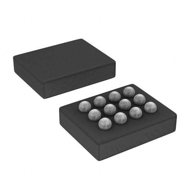
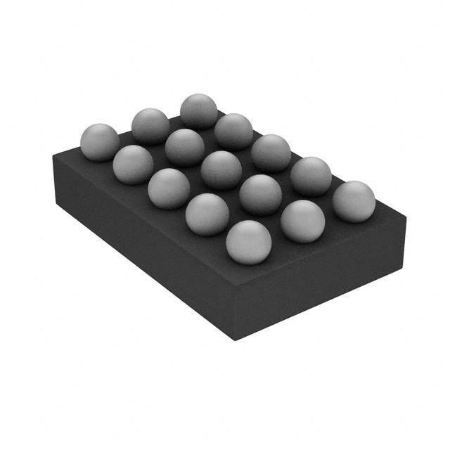
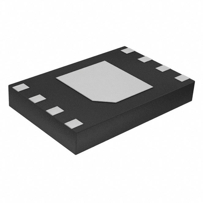
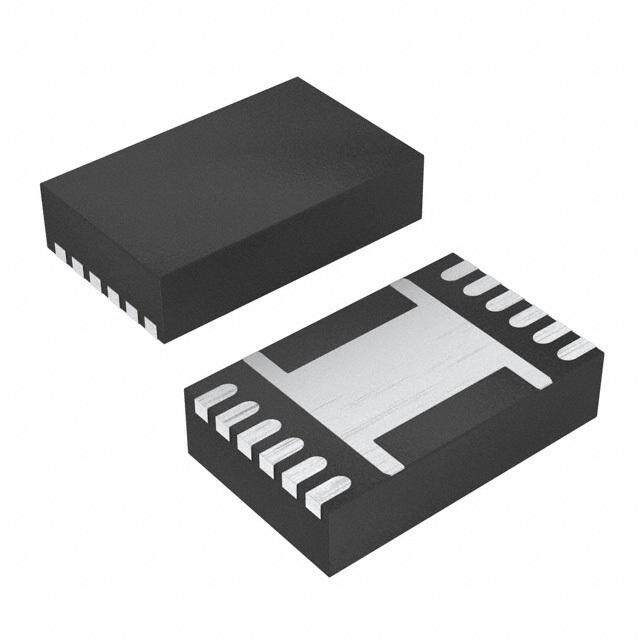
| 供应商器件封装 | 48-VQFN(7x7) |
| 其它名称 | 296-31474-6 |
| 功能 | 电池监控器 |
| 包装 | Digi-Reel® |
| 商标 | Texas Instruments |
| 安装类型 | 表面贴装 |
| 安装风格 | SMD/SMT |
| 封装 | Reel |
| 封装/外壳 | 48-VFQFN 裸露焊盘 |
| 封装/箱体 | VQFN-48 |
| 工作温度 | -40°C ~ 85°C |
| 工厂包装数量 | 250 |
| 最大工作温度 | + 85 C |
| 最小工作温度 | - 40 C |
| 标准包装 | 1 |
| 电压-电源 | 2.3 V ~ 4.5 V |
| 电池化学 | 锂离子 |
| 电池类型 | Li-Ion |
| 系列 | BQ78PL114 |


PDF Datasheet 数据手册内容提取
bq78PL114 www.ti.com................................................................................................................................................ SLUS850B–SEPTEMBER2008–REVISEDAPRIL2009 PowerLAN™ Master Gateway Battery Management Controller With PowerPump™ Cell Balancing Technology FEATURES – bq78PL114S12:<300m AActive,<185m A 1 • bq78PL114DesignedforManaging3-to Standby,<85m AShip,and<1m A 23 8-Series-CellBatterySystems UndervoltageShutdown • bq78PL114S12FirmwareUpgradeSupports3- • Accurate,AdvancedTemperatureMonitoring to12-Series-CellBatterySystems ofCellsandMOSFETsWithupto12Sensors – AddsSupportforLCDandElectronicPaper • Fail-SafeOperationofPackProtection DisplaysorEPDs Circuits:UptoThreePowerMOSFETsand OneSecondarySafetyOutput(Fuse) – Configurablefor11-A,26-A,or110-A OperatingCurrents • FullyProgrammableVoltage,Current,Balance, • SystemsWithMoreThanFourSeriesCells andTemperature-ProtectionFeatures RequireExternalbq76PL102Dual-Cell • ExternalInputsforAuxiliaryMOSFETControl Monitors • SmartBatterySystem1.1Compliantvia • SmartSafetyFeatures: SMBus – Prevention:OptimalCellManagement APPLICATIONS – Diagnosis:ImprovedSensingofCell • PortableMedicalInstrumentsandTest Problems Equipment – FailSafe:DetectionofEventPrecursors • MobilityDevices(E-Bike) • Rate-of-ChangeDetectionofAllImportantCell • UninterruptiblePowerSuppliesandHand-Held Characteristics: Tools – Voltage DESCRIPTION – Impedance – CellTemperature The bq78PL114 master gateway battery controller is • PowerPumpTechnologyTransfersCharge part of a complete Li-Ion control, monitoring, and safetysolutiondesignedforlargeseriescellstrings. EfficientlyFromCelltoCellDuringAll OperatingConditions,ResultinginLonger The bq78PL114 and bq78PL114S12 along with RunTimeandCellLife bq76PL102 PowerLAN™ dual-cell monitors provide complete battery-system control, communications, – bq78PL114S12AddsUser-Configurable and safety functions for a structure of three up to PowerPumpCell-BalancingModes twelve series cells. This PowerLAN system provides • High-Resolution18-BitIntegratingDelta-Sigma simultaneous, synchronized voltage and current CoulombCounterforPreciseCharge-Flow measurements using one A/D per-cell technology. MeasurementsandGasGauging This eliminates system-induced noise from • MultipleIndependentΔ-ΣADCs:One-per-Cell measurements and allows the precise, continuous, real-time calculation of cell impedance under all Voltage,PlusSeparateTemperature,Current, operating conditions, even during widely fluctuating andSafety loadconditions. • Simultaneous,SynchronousMeasurementof PackCurrentandIndividualCellVoltages PowerPump technology transfers charge between cells to balance their voltage and capacity. Balancing • VeryLowPowerConsumption is possible during all battery modes: charge, – bq78PL114:<250m AActive,<150m A discharge, and rest. Highly efficient charge-transfer Standby,<40m AShip,and<1m A circuitry nearly eliminates energy loss while providing UndervoltageShutdown true real-time balance between cells, resulting in longerrun-timeandimprovedcyclelife. 1 Pleasebeawarethatanimportantnoticeconcerningavailability,standardwarranty,anduseincriticalapplicationsofTexas Instrumentssemiconductorproductsanddisclaimerstheretoappearsattheendofthisdatasheet. PowerLAN,PowerPump,bqWizardaretrademarksofTexasInstruments. 2 Allothertrademarksarethepropertyoftheirrespectiveowners. 3 PRODUCTIONDATAinformationiscurrentasofpublicationdate. Copyright©2008–2009,TexasInstrumentsIncorporated Products conform to specifications per the terms of the Texas Instruments standard warranty. Production processing does not necessarilyincludetestingofallparameters.
bq78PL114 SLUS850B–SEPTEMBER2008–REVISEDAPRIL2009................................................................................................................................................ www.ti.com Thesedeviceshavelimitedbuilt-inESDprotection.Theleadsshouldbeshortedtogetherorthedeviceplacedinconductivefoam duringstorageorhandlingtopreventelectrostaticdamagetotheMOSgates. DESCRIPTION (CONTINUED) Temperature is sensed by up to 12 external sensors and one on-chip sensor. This permits accurate temperature monitoring of each cell individually. Firmware is then able to compensate for the temperature-induced effects on capacity, impedance, and OCV on a cell-by-cell basis, resulting in superior charge/ discharge and balancing control. External MOSFET control inputs provide user- definable direct hardware control over MOSFET states. Smart control prevents excessive current through MOSFET body diodes. Auxiliary inputs can be used for enhanced safetyandcontrolinlargemulticellarrays. The bq78PL114 is completely user-configurable, with parametric tables in flash memory to suit a variety of cell chemistries, operating conditions, safety controls, and data reporting needs. It is easily configured using the supplied bqWizard™ graphical user interface (GUI). The device is fully programmed and requires no algorithm or firmwaredevelopment. The bq78PL114 can be upgraded to the bq78PL114S12 by downloading the bq78PL114S12 firmware. The firmware can be downloaded using the bqWizard application or during manufacturing. Upgrading to the bq78Pl114S12 changes the functionality of the LED1–LED5, LEDEN, and N/C pin #29. The bq78PL114S12 pin functions of LED1/SEG1–LED5/SEG5, PSH/BP/TP, and FIELD support LED, LCD, and electronic paper displays (EPDs).Theusercanconfigurethebq78PL114S12forthedesireddisplaytype. In this document all descriptions for the bq78PL114 apply to the bq78PL114S12 except where different bq78PL114S12functionalityisspecificallydescribed. 2 SubmitDocumentationFeedback Copyright©2008–2009,TexasInstrumentsIncorporated ProductFolderLink(s):bq78PL114
bq78PL114 www.ti.com................................................................................................................................................ SLUS850B–SEPTEMBER2008–REVISEDAPRIL2009 P-LAN V4 PRE Voltage 4 P4N L CHG P4S BTeamlapnce CEL ASH First-Leavnedl Safety DSG XT4 L FETControl EFCID F EFCIC V3 Voltage 3 P3N L P3S Balance EL SPROT Temp C Second-Level XT3 RISC Safety CSBAT CPU CSPACK V2 Voltage M P2N L2 RA P2S Balance EL S CoulombCounter CCBAT Temp C XT2 CurrentA/D CCPACK V1 P1N Voltage L1 PowerLAN 6 LED1–5, Balance L Communication GPIO P1S E LEDEN Temp C Link XT1 SMBCLK SMBus Reset Internal SMBDAT RSTN Logic Oscillator Internal VLDO1 2.5 V LDO Watchdog Temperature Core/CPU I/O Measure Safety B0320-02 Figure1.bq78PL114InternalBlockDiagram Copyright©2008–2009,TexasInstrumentsIncorporated SubmitDocumentationFeedback 3 ProductFolderLink(s):bq78PL114
bq78PL114 SLUS850B–SEPTEMBER2008–REVISEDAPRIL2009................................................................................................................................................ www.ti.com P-LAN V4 PRE Voltage 4 P4N L CHG P4S BTeamlapnce CEL ASH First-Leavnedl Safety DSG XT4 L FETControl EFCID F EFCIC V3 Voltage 3 P3N L P3S Balance EL SPROT Temp C Second-Level XT3 RISC Safety CSBAT CPU CSPACK V2 Voltage M P2N L2 RA P2S Balance EL S CoulombCounter CCBAT Temp C XT2 CurrentA/D CCPACK V1 P1N Voltage L1 PowerLAN 7 LED1–5/SEG1–5, Balance L Communication GPIO PSH/BP/TP, P1S Temp CE Link FIELD XT1 SMBCLK SMBus Reset Internal SMBDAT RSTN Logic Oscillator Internal VLDO1 2.5 V LDO Watchdog Temperature Core/CPU I/O Measure Safety B0320-03 Figure2.bq78PL114S12InternalBlockDiagram 4 SubmitDocumentationFeedback Copyright©2008–2009,TexasInstrumentsIncorporated ProductFolderLink(s):bq78PL114
bq78PL114 www.ti.com................................................................................................................................................ SLUS850B–SEPTEMBER2008–REVISEDAPRIL2009 Pack Pack Negative Positive s u – B + M S Example 8-cell configuration shown e ns ou RSENSE BMaatbPtseqtore7ywr8 eCGProLLan1Atet1Nrwo4laleyr Pack ProtectiCircuits and F n o werLANmunicatiLink Poom bqM7o6nPiLto1r0 W2iCthell bqM7o6nPiLto1r0 W2iCthell C PowerPump PowerPump Balancing Balancing B0332-01 Figure3.Examplebq78PL114PowerLANMulticellSystemImplementation(8Cells) Copyright©2008–2009,TexasInstrumentsIncorporated SubmitDocumentationFeedback 5 ProductFolderLink(s):bq78PL114
bq78PL114 SLUS850B–SEPTEMBER2008–REVISEDAPRIL2009................................................................................................................................................ www.ti.com Packositive CPiraccukit sP raontde cFtiuosne B0332-02 P or T2 L102Monit V2 12 6Pell Bq7al-C T1 u D V1 11 or T2 102Monit V2 10 L 6Pell 7C 1 bqal- T u D V1 9 n w o sh or T2 ation L102Monit V2 8 gur 6Pell onfi Bq7al-C T1 ell c Du V1 7 c 2- 1 e mpl or T2 Exa 102Monit V2 6 L 6Pell 7C 1 CoPmomwuenrLicAaNtion bqDual- TV1 5 Link er 4T oll X ontr V4 4 C y 12 NerS 3 PowerLAway Batt78PL114 V3XT 3 eq atb G 2 SMBus Master V2XT 2 1 T X V1 1 e PackNegativ RSENSE Figure4.Examplebq78PL114S12SystemImplementation(12Cells) 6 SubmitDocumentationFeedback Copyright©2008–2009,TexasInstrumentsIncorporated ProductFolderLink(s):bq78PL114
bq78PL114 www.ti.com................................................................................................................................................ SLUS850B–SEPTEMBER2008–REVISEDAPRIL2009 ORDERINGINFORMATION Product CellConfiguration(1) Package Package Temperature OrderingNumber Quantity, Designator Range TransportMedia QFN-48,7-mm bq78PL114RGZT 250,tapeandreel bq78PL114 3to8seriescells RGZ –40°Cto85°C ×7-mm bq78PL114RGZR 2500,tapeandreel bq78PL114S Firmwaredownload 3to12seriescells N/A N/A N/A N/A 12 andupgrade (1) Forconfigurationsconsistingofmorethanfourseriescells,additionalbq76PL102partsmustbeused. AVAILABLE OPTIONS bq78PL114 RGZ Package (Top View) T K 2 A L O D C SS 1 T1 T2 2 LD 3 T3 T4 4 MB MB V V X X V V V X X V S S 8 7 6 5 4 3 2 1 0 9 8 7 CHG 14 4 4 4 4 4 4 4 4 3 3 336 LED5 DSG 2 35 LED4 PRE 3 34 LED3 EFCIC 4 33 LED2 EFCID 5 32 LED1 CCBAT 6 31 LEDEN Thermal Pad CCPACK 7 30 SPROT VLDO1 8 29 NC CSBAT 9 28 NC CSPACK 10 27 NC OSCI 11 26 NC OSCO 12 25 RSTN 3 4 5 6 7 8 9 0 1 2 3 4 1 1 1 1 1 1 1 2 2 2 2 2 0 1 N S N 2 3 S N S N N O DI 1 2 2 O DI 3 3 4 4 A D S P P P D S P P P P L S S P- P0023-16 Figure5.bq78PL114Pinout bq78PL114TERMINALFUNCTIONS NAME NO. TYPE(1) DESCRIPTION CCBAT 6 IA Coulombcounterinput(senseresistor),connecttobatterynegative CCPACK 7 IA Coulombcounterinput(senseresistor),connecttopacknegative CHG 1 O ChargeMOSFETcontrol(active-high,lowopensMOSFET) CSBAT 9 IA Currentsenseinput(safety),connecttobatterynegative CSPACK 10 IA Currentsenseinput(safety),connecttopacknegative DSG 2 O DischargeMOSFETcontrol(active-high,lowopensMOSFET) EFCIC 4 I ExternalchargeMOSFETcontrolinput (1) I–input,IA–analoginput,O–output,OA–analogoutput,P–power Copyright©2008–2009,TexasInstrumentsIncorporated SubmitDocumentationFeedback 7 ProductFolderLink(s):bq78PL114
bq78PL114 SLUS850B–SEPTEMBER2008–REVISEDAPRIL2009................................................................................................................................................ www.ti.com bq78PL114TERMINALFUNCTIONS(continued) NAME NO. TYPE(1) DESCRIPTION EFCID 5 I ExternaldischargeMOSFETcontrolinput LED1 32 O LED1–open-drain,active-low LED2 33 O LED2–open-drain,active-low LED3 34 O LED3–open-drain,active-low LED4 35 O LED4–open-drain,active-low LED5 36 O LED5–open-drain,active-low LEDEN 31 IO LEDEN–common-anodedrive(active-low)andpushbuttoninput NC 26 IO Connect1-MΩresistortoVSS NC 27 I Connect1-MΩresistortoVSS NC 28,29 O Noconnect OSCI 11 I Externaloscillatorinput(noconnect,internaloscillatorused) OSCO 12 O Externaloscillatoroutput(noconnect,internaloscillatorused) P1N 15 O Charge-balancegatedrive,cell1north P2S 16 O Charge-balancegatedrive,cell2south P2N 17 O Charge-balancegatedrive,cell2north P3N 21 O Charge-balancegatedrive,cell3north P3S 20 O Charge-balancegatedrive,cell3south P4N 23 O Charge-balancegatedrive,cell4north P4S 22 O Charge-balancegatedrive,cell4south P-LAN 24 IO PowerLANI/Otoexternalbq76PL102nodes PRE 3 O PrechargeMOSFETcontrol(active-high) RSTN 25 I Devicereset,active-low SDI1 14 I ConnecttoSDO0viaacapacitor SDI3 19 I InternalPowerLANconnection–connecttoSDO2througha0.01-m Fcapacitor SDO0 13 O Requires100-kΩpullupresistortoVLDO1 SDO2 18 O InternalPowerLANconnection–connecttoSDI3througha0.01-m Fcapacitor SMBCLK 37 IO SMBusclocksignal SMBDAT 38 IO SMBusdatasignal SPROT 30 O Secondaryprotectionoutput,active-high(FUSE) V1 47 IA Cell-1positiveinput V2 44 IA Cell-2positiveinput V3 42 IA Cell-3positiveinput V4 39 IA Cell-4positiveinput VLDO1 8 P InternalLDO-1output,bypasswith10-m FcapacitortoVSS VLDO2 43 P InternalLDO-2output,bypasswith10-m FcapacitortoV2 VSS 48 IA Cell-1negativeinput XT1 46 IA Externaltemperature-sensor-1input XT2 45 IA Externaltemperature-sensor-2input XT3 41 IA Externaltemperature-sensor-3input XT4 40 IA Externaltemperature-sensor-4input – – P Thermalpad.ConnecttoVSS 8 SubmitDocumentationFeedback Copyright©2008–2009,TexasInstrumentsIncorporated ProductFolderLink(s):bq78PL114
bq78PL114 www.ti.com................................................................................................................................................ SLUS850B–SEPTEMBER2008–REVISEDAPRIL2009 bq78PL114S12 RGZ Package (Top View) T K 2 A L O D C SS 1 T1 T2 2 LD 3 T3 T4 4 MB MB V V X X V V V X X V S S 8 7 6 5 4 3 2 1 0 9 8 7 CHG 14 4 4 4 4 4 4 4 4 3 3 336 LED5/SEG5 DSG 2 35 LED4/SEG4 PRE 3 34 LED3/SEG3 EFCIC 4 33 LED2/SEG2 EFCID 5 32 LED1/SEG1 CCBAT 6 31 PSH/BP/TP Thermal Pad CCPACK 7 30 SPROT VLDO1 8 29 FIELD CSBAT 9 28 NC CSPACK 10 27 NC OSCI 11 26 NC OSCO 12 25 RSTN 3 4 5 6 7 8 9 0 1 2 3 4 1 1 1 1 1 1 1 2 2 2 2 2 0 1 N S N 2 3 S N S N N O DI 1 2 2 O DI 3 3 4 4 A D S P P P D S P P P P L S S P- P0023-20 Figure6.bq78PL114S12Pinout bq78PL114S12TERMINALFUNCTIONS NAME NO. TYPE(1) DESCRIPTION CCBAT 6 IA Coulombcounterinput(senseresistor),connecttobatterynegative CCPACK 7 IA Coulombcounterinput(senseresistor),connecttopacknegative CHG 1 O ChargeMOSFETcontrol(active-high,lowopensMOSFET) CSBAT 9 IA Currentsenseinput(safety),connecttobatterynegative CSPACK 10 IA Currentsenseinput(safety),connecttopacknegative DSG 2 O DischargeMOSFETcontrol(active-high,lowopensMOSFET) EFCIC 4 I ExternalchargeMOSFETcontrolinput EFCID 5 I ExternaldischargeMOSFETcontrolinput FIELD 29 O EPDfieldsegment LED1/SEG1 32 O LED1–open-drain,active-low,LCDandEPDsegment1 LED2/SEG2 33 O LED2–open-drain,active-low,LCDandEPDsegment2 LED3/SEG3 34 O LED3–open-drain,active-low,LCDandEPDsegment3 LED4/SEG4 35 O LED4–open-drain,active-low,LCDandEPDsegment4 LED5/SEG5 36 O LED5–open-drain,active-low,LCDandEPDsegment5 N/C 26,27 IO Connect1-MΩresistortoVSS N/C 28 O Noconnect OSCI 11 I Externaloscillatorinput(noconnect,internaloscillatorused) (1) I–input,IA–analoginput,O–output,OA–analogoutput,P–power Copyright©2008–2009,TexasInstrumentsIncorporated SubmitDocumentationFeedback 9 ProductFolderLink(s):bq78PL114
bq78PL114 SLUS850B–SEPTEMBER2008–REVISEDAPRIL2009................................................................................................................................................ www.ti.com bq78PL114S12TERMINALFUNCTIONS(continued) NAME NO. TYPE(1) DESCRIPTION OSCO 12 O Externaloscillatoroutput(noconnect,internaloscillatorused) P1N 15 O Charge-balancegatedrive,cell1north P2N 17 O Charge-balancegatedrive,cell2north P2S 16 O Charge-balancegatedrive,cell2south P3N 21 O Charge-balancegatedrive,cell3north P3S 20 O Charge-balancegatedrive,cell3south P4N 23 O Charge-balancegatedrive,cell4north P4S 22 O Charge-balancegatedrive,cell4south P-LAN 24 IO PowerLANI/Otoexternalbq76PL102nodes PRE 3 O PrechargeMOSFETcontrol(active-high) PSH/BP/TP 31 IO PushbuttondetectforLEDdisplay,LCDbackplane,EPDtopplaneandchargepump RSTN 25 I Devicereset,active-low SDI1 14 I ConnecttoSDO0viaacapacitor SDI3 19 I InternalPowerLANconnection–connecttoSDO2througha0.01-m Fcapacitor SDO0 13 O Requires100-kΩpullupresistortoVLDO1 SDO2 18 O InternalPowerLANconnection–connecttoSDI3througha0.01-m Fcapacitor SMBCLK 37 IO SMBusclocksignal SMBDAT 38 IO SMBusdatasignal SPROT 30 O Secondaryprotectionoutput,active-high(FUSE) V1 47 IA Cell-1positiveinput V2 44 IA Cell-2positiveinput V3 42 IA Cell-3positiveinput V4 39 IA Cell-4positiveinput VLDO1 8 P InternalLDO-1output,bypasswith10-m FcapacitortoVSS VLDO2 43 P InternalLDO-2output,bypasswith10-m FcapacitortoV2 VSS 48 IA Cell-1negativeinput XT1 46 IA Externaltemperature-sensor-1input XT2 45 IA Externaltemperature-sensor-2input XT3 41 IA Externaltemperature-sensor-3input XT4 40 IA Externaltemperature-sensor-4input – – P Thermalpad.ConnecttoVSS 10 SubmitDocumentationFeedback Copyright©2008–2009,TexasInstrumentsIncorporated ProductFolderLink(s):bq78PL114
bq78PL114 www.ti.com................................................................................................................................................ SLUS850B–SEPTEMBER2008–REVISEDAPRIL2009 ABSOLUTE MAXIMUM RATINGS(1) overoperatingfree-airtemperaturerange(unlessotherwisenoted) RANGE UNITS T Operatingfree-airtemperature(ambient) –40to85 °C A T Storagetemperature –65to150 °C stg V4–V3 Maximumcellvoltage –0.5to5.0 V V3–V2 Maximumcellvoltage –0.5to5.0 V V2–V1 Maximumcellvoltage –0.5to5.0 V V1–VSS Maximumcellvoltage –0.5to5.0 V VoltageonLEDEN,SPROT,CCBAT, CCPACK,CSBAT,CSPACK,XT1,XT2, MaximumvoltageonanyI/OpinwithrespecttoVSS –0.5to(VLDO1+0.5) V OSCI,OSCO,P-LAN VoltageonPSH/BP/TP(bq78PL114S12) MaximumvoltagerangewithrespecttoVSS –0.5to(VLDO1+0.5) V VoltageonLED1–LED5 MaximumvoltageonI/OpinwithrespecttoVSS –0.5to5.5 V VoltageonLED1/SEG1–LED5/SEG5 MaximumvoltageonI/Opin –0.5to5.5 V (bq78PL114S12) (V2–0.5)to VoltageonXT3,XT4 MaximumvoltagerangewithrespecttoV2 V (VLDO2+0.5) EFCIC,EFCID MaximumvoltagerangewithrespecttoVSS –0.5to5.5 V VoltageonSMBCLK,SMBDAT MaximumvoltagerangewithrespecttoVSS –0.5to6 V VoltageonPRE,CHG,DSG MaximumvoltagerangewithrespecttoVSS –0.5to(VLDO1+0.5) V CurrentthroughPRE,CHG,DSG, Maximumcurrentsource/sink 20 mA LED1–LED5,P-LAN Currentthrough LED1/SEG1–LED5/SEG5, Maximumcurrentsource/sink 20 mA (bq78PL114S12,LEDmode) VLDO1maximumcurrent MaximumcurrentdrawfromVLDO 20 mA JEDEC,JESD22-A114human-bodymodel,R=1500Ω,C= ESDtolerance 2 kV 100pF Leadtemperature,soldering Totaltime<3seconds 300 °C (1) StressesbeyondthoselistedunderAbsoluteMaximumRatingsmaycausepermanentdamagetothedevice.Thesearestressratings only,andfunctionaloperationofthedeviceattheseoranyotherconditionsbeyondthoseindicatedunderRecommendedOperating Conditionsisnotimplied.Exposuretoabsolute-maximum-ratedconditionsforextendedperiodsmayaffectdevicereliability. RECOMMENDED OPERATING CONDITIONS overoperatingfree-airtemperaturerange(unlessotherwisenoted) MIN NOM MAX UNIT V Supplyvoltage—V1,V2,V3,V4 2.3 4.5 V SUP V Minimumstartupvoltage—V1,V2 2.9 V Startup V Inputcellvoltagerange—V(n+1)–V(n),n=1,2,3,4 0 4.5 V IN C VLDO1capacitor—VLDO1 2.2 10 47 m F VLDO1 C VLDO2capacitor—VLDO2 2.2 10 47 m F VLDO2 C Cell-voltagecapacitor—Vn 1 m F Vn Copyright©2008–2009,TexasInstrumentsIncorporated SubmitDocumentationFeedback 11 ProductFolderLink(s):bq78PL114
bq78PL114 SLUS850B–SEPTEMBER2008–REVISEDAPRIL2009................................................................................................................................................ www.ti.com ELECTRICAL CHARACTERISTICS T =–40°Cto85°C(unlessotherwisenoted) A DC Characteristics PARAMETER TESTCONDITIONS MIN TYP MAX UNIT V (1) Operatingrange Cellsbalanced 2.3 4.5 V CELL I Operating-modecurrent Measure/reportstate,bq78PLL114 250 m A DD Measure/reportstate,bq78PLL114S12 300 I Standby-modecurrent SMBCLK=SMBDAT=L,bq78PLL114 100 m A STBY SMBCLK=SMBDAT=L, 185 bq78PLL114S12 I Ship-modecurrent bq78PLL114 30 m A SHIP bq78PLL114S12 85 I Extremecellundervoltage Allcells<2.7Vandanycell<ECUVset 1 m A ECUV shutdowncurrent point V SPROT,LEDEN, I <4mA 0 0.5 V OL OL PSH/BP/TP(bq78PL114S12), FIELD(bq78PL114S12) V (2) SPROT,LEDEN, I <–4mA V –0.1 V OH OH LDO1 PSH/BP/TP(bq78PL114S12), FIELD(bq78PL114S12) V SPROT,LEDEN, 0.25V V IL LDO1 PSH/BP/TP(bq78PL114S12), FIELD(bq78PL114S12) V SPROT,LEDEN, 0.75V V IH LDO1 PSH/BP/TP(bq78PL114S12), FIELD(bq78PL114S12) (1) Deviceshouldbeconfiguredtoentershutdownstatewhencellvoltagesarebelow2.5V. (2) DoesnotapplytoSMBuspins. Voltage-Measurement Characteristics overoperatingfree-airtemperaturerange(unlessotherwisenoted) PARAMETER TESTCONDITIONS MIN TYP MAX UNIT Measurementrange 2.5 4.5 V Resolution <1 mV 25°C ±5 Accuracy mV 0°Cto60°C ±10 12 SubmitDocumentationFeedback Copyright©2008–2009,TexasInstrumentsIncorporated ProductFolderLink(s):bq78PL114
bq78PL114 www.ti.com................................................................................................................................................ SLUS850B–SEPTEMBER2008–REVISEDAPRIL2009 Current-Sense Characteristics overoperatingfree-airtemperaturerange(unlessotherwisenoted) PARAMETER TESTCONDITIONS MIN TYP MAX UNIT Measurementrange(1)(bq78PL114) –0.2 0.2 V Measurementrange(2)(bq78PL114S12,3-mΩ –0.077 0.077 V senseresistor) Measurementrange(2)(bq78PL114S12,1-mΩ –0.1 0.1 V and10-mΩsenseresistors) Inputoffset T =25°C ±50 m V A Offsetdrift T =0°Cto60°C 0.5 m V/°C A Resolution(bq78PL114) 18 m V Resolution(bq78PL114S12,3-mΩsense 6.9 m V resistor) Resolution(bq78PL114S12,1-mΩand10-mΩ 10 m V senseresistors) Full-scaleerror(3) T =25°C ±0.1% A Full-scaleerrordrift T =0°Cto60°C 50 PPM/°C A (1) Defaultrange.Correspondsto±10Ausinga5-mΩsenseresistor. (2) Thebq78PL114S12firmwareupgradesupportsthreesense-resistoroptions,10mΩ,3mΩ,and1mΩ. (3) Aftercalibration.Accuracyisdependentonsystemcalibrationandtemperaturecoefficientofsenseresistor. Coulomb-Counter Characteristics(1) (2) overoperatingfree-airtemperaturerange(unlessotherwisenoted) PARAMETER TESTCONDITIONS MIN TYP MAX UNIT Resolution 5 nVh Intergralnonlinearity 0.008% Snap-to-zero(deadband) ±100(3) m V (1) Sharescommoninputwithcurrent-sensesection (2) Aftercalibration.accuracyisdependentonsystemcalibrationandtemperaturecoefficientofsenseresistor. (3) Correspondsto20mAusing5-mΩsenseresistor Current-Sense (Safety) Characteristics(1) overoperatingfree-airtemperaturerange(unlessotherwisenoted) PARAMETER TESTCONDITIONS MIN TYP MAX UNIT Measurementrange –0.312 0.312 V Short-circuitdetection 10 Resolution mV Overcurrentdetection,chargeanddischarge 1.25 (1) Postcalibration:Dependentonsystemcalibrationandtemperaturecoefficientofsenseresistor.Uncertaintyis1.5LSB. Internal Temperature-Sensor Characteristics(1) overoperatingfree-airtemperaturerange(unlessotherwisenoted) PARAMETER TESTCONDITIONS MIN TYP MAX UNIT Measurementrange –30 85 °C Resolution 0.1 °C Accuracy(1) –30°to85° ±1 °C (1) Aftercalibration Copyright©2008–2009,TexasInstrumentsIncorporated SubmitDocumentationFeedback 13 ProductFolderLink(s):bq78PL114
bq78PL114 SLUS850B–SEPTEMBER2008–REVISEDAPRIL2009................................................................................................................................................ www.ti.com LDO Voltage Characteristics(1) overoperatingfree-airtemperaturerange(unlessotherwisenoted) PARAMETER TESTCONDITIONS MIN TYP MAX UNIT V LDO1operatingvoltage,referencedto T =–40Cto85C,load=200m A 2.425 2.5 2.575 V LDO1 A VSS V LDO2operatingvoltage,referencedtoV2 T =–40Cto85C,load=2mA 2.425 2.5 2.575 V LDO2 A (1) Aftercalibration External Temperature-Sensor(s) Typical Characteristics(1) overoperatingfree-airtemperaturerange(unlessotherwisenoted) PARAMETER TESTCONDITIONS MIN TYP MAX UNIT Measurementrange(2) –40 90 °C Resolution 0.2 °C 25° ±1 Accuracy(3) °C 0°to85° ±2 (1) Typicalfordual-diode(MMBD4148orequivalent)externalsensorusingrecommendedcircuit (2) RangeofdiodesensorsmayexceedoperationallimitsofICandbatterycells. (3) Typicalbehavioraftercalibration,finalresultdependentonspecificcomponentcharacteristics SMBus Characteristics(1) overoperatingfree-airtemperaturerange(unlessotherwisenoted) PARAMETER TESTCONDITIONS MIN TYP MAX UNIT V Inputlowvoltage 0 0.8 V IL V Inputhighvoltage 2.1 5.5 V IH V Outputlowvoltage 350-m Asinkcurrent 0 0.4 V OL C Capacitance,eachI/Opin 10 pF I f SCLKnominalclockfrequency T =25°C 100 kHz SCL A V 5Vnominal 13.3 45.3 R (2) PullupresistorsforSCLK,SDATA BUS kΩ PU V 3Vnominal 2.4 6.8 BUS (1) SMBustimingandsignalsmeettheSMBus2.0specificationrequirementsundernormaloperatingconditions.Allsignalsaremeasured withrespecttoPACK-negative. (2) Pullupsaretypicallyimplementedexternaltothebatterypack,andareselectedtomeetSMBusrequirements. 14 SubmitDocumentationFeedback Copyright©2008–2009,TexasInstrumentsIncorporated ProductFolderLink(s):bq78PL114
bq78PL114 www.ti.com................................................................................................................................................ SLUS850B–SEPTEMBER2008–REVISEDAPRIL2009 R PRE + PACK+ Level-Shift Circuits G G E S H R D C P SDI1 SDO2 SDO0 SDI3 VLDO1 g V2 n 2 CELL6 Cell BalanciCircuits V1 bq76PL10 P-LAN RSTN CELL5 SPROT V4 bq78PL114 CELL4 PowerLAN 5 Gateway Battery LED1–LED5 s uit Management Circ V3 Controller CELL3 ng CELL2 Cell Balanci VV2LDO2 EEFFCCIICD ction Aux FETControl e ot Pr V1 D CELL1 SMBCLK ES us B XT1–XT4 SMBDAT M S Temperature Sensor (typ.) d a P CRFI hermal SS SBAT CBAT CPACK SACPK T V C C C C One of 4 external sensors shown – PACK– Typical six-cell configuration shown. R Additional cells added via PowerLAN connection. SENSE Some components omitted for clarity. S0342-02 Figure7.bq78PL114SimplifiedExampleCircuitDiagram Copyright©2008–2009,TexasInstrumentsIncorporated SubmitDocumentationFeedback 15 ProductFolderLink(s):bq78PL114
bq78PL114 SLUS850B–SEPTEMBER2008–REVISEDAPRIL2009................................................................................................................................................ www.ti.com FEATURE SET Primary(First-Level)SafetyFeatures The bq78PL114 implements a breadth of system protection features which are easily configured by the customer.First-levelprotectionsworkbycontrollingtheMOSFETswitches.Theseinclude: • Batterycellover/undervoltageprotection • Packover/undervoltageprotection • Chargeanddischargeovercurrentprotection • Short-circuitprotection • ExternalMOSFETcontrolinputs(EFCIx)withprogrammablepolarity • Upto12externaltemperatureinputsforaccuratecellandMOSFETmonitoring • Watchdogtimerprotection • Brownoutdetectionandprotectionagainstextremepackundervoltage Secondary(Second-Level)SafetyFeatures The bq78PL114 can detect more serious system faults and activate the SPROT pin, which can be used to open anin-linechemicalfusetopermanentlydisablethepack.Secondaryoptionalfeaturesinclude • Fullyindependentoffirst-levelprotections • SmartSafetyalgorithmsforearlydetectionofpotentialfaults – Temperatureabnormalities(variances,extremes,rateofchange,etc.) – Disconnectedcellvoltageinputs – Cellimbalanceexceedssafetylimits – Impedanceriseduetocellorweldstrapfault • MOSFETfailureorlossofMOSFETcontrol • Safetyovervoltage,packandcell • Safetyovertemperature,limitsforbothchargeanddischarge • Safetyovercurrent,chargeanddischarge • Failedcurrentmeasurement,voltagemeasurement,ortemperaturemeasurement ChargeControlFeatures • MeetsSMBus2.0andSmartBatterySystem(SBS)Specification1.1requirements • Active cell balancing using patented PowerPump technology, which eliminates unrecoverable capacity loss duetonormalcellimbalance • Balancing-currentmonitoringtodetectcellproblems • Simultaneous,synchronousmeasurementofallcellvoltagesinapack • Simultaneous,synchronousmeasurementofpackcurrentwithcellvoltages • Reportstargetchargingcurrentand/orvoltagetoanSBSSmartCharger • Reportsthechemicalstate-of-chargeforeachcellandpack • Supportsprechargingandzero-voltchargingwithseparateMOSFETcontrol • Programmable,Chemistry-specificparameters • Faultreporting GasGauging • The bq78PL114 accurately reports battery cell and pack state-of-charge (SOC). No full charge/discharge cycleisrequiredforaccuratereporting. • State-of-chargeisreportedviaSMBusandoptionaldisplay. • 18-bitintegratingdelta-sigmaADCcoulombcounter,withprogrammablesnap-to-zerovalue DisplayTypes • The bq78PL114 drives a three- to five-segment LED display in response to a pushbutton (LEDEN) input signal.EachLEDpincansinkupto10mA. 16 SubmitDocumentationFeedback Copyright©2008–2009,TexasInstrumentsIncorporated ProductFolderLink(s):bq78PL114
bq78PL114 www.ti.com................................................................................................................................................ SLUS850B–SEPTEMBER2008–REVISEDAPRIL2009 • Thebq78PL114S12drivesathree-tofive-segmentstaticliquid-crystaldisplay. • The bq78PL114S12 drives a three- to five-segment electronic paper display. An external 15-V voltage source isrequired.EInkCorporationsuppliesthistypeofdisplay. Thedisplaytypeisselectedviatheparameterset. LifetimeLogging(ReadableviaSMBus) • Recordingoffaults,events,anomalies,minimumandmaximumvalues • Maximum/minimumtemperature • Maximum/minimumpackvoltage • Maximum/minimumcellvoltageinapack • Maximumchargeanddischargecurrents ForensicDataLogging(ReadableviaSMBus) • Lastknownfullcapacityofeachcell • Cyclecountand/orcumulativenumberofampere-hoursdeliveredbythebattery • Batterypackstatus:beingcharged,discharged,oratrest • Balancingeffortrequiredbyeachbankofcellstomaintainbalance • Last10failurescausingfirst-levelsafetyaction • Forensicdataup-loadabletohostCPUviaSMBus PowerModes • Normal Mode: The bq78PL114 performs measurements and calculations, makes decisions, and updates internaldataapproximatelyoncepersecond.Allsafetycircuitryisfullyfunctionalinthismode. • Standby Mode: The bq78PL114 performs as in normal mode, but at a dramatically reduced rate to lower power consumption at times when the host computer is inactive or the battery system is not being used. All safetycircuitryremainsfullyfunctionalinthismode. • Ship Mode: The bq78PL114 disables (opens) all the protection MOSFETs, and continues to monitor temperature and voltage, but at a reduced measurement rate to dramatically lower power consumption. Environmentaldataissavedinflashasa part of the historical record. Safety circuitry is disabled in this mode. The device does not enter this power state as a part of normal operation; it is intended for use after factory programming and test. Entry occurs only after a unique SMBus command is issued. Exit occurs when the SMBuslinesreturntoanactivestate. • Extreme Cell Undervoltage (ECUV) Shutdown Mode: In this mode, the bq78PL114 draws minimal current and the charge and discharge protection MOSFETs are disabled (opened). The precharge MOSFET remains enabledwhenachargevoltageispresent.Safetycircuitryis disabled in this mode. The device does not enter this mode as a part of normal operation; it enters this state during extreme cell undervoltage conditions (ECUV).TheECUVthresholdisprogrammablebetween2.3Vand2.7V,with2.5Vbeingtypical. OVERCURRENT STATE ENTRYCONDITION EXITCONDITION PROTECTION Normaloperationasdeterminedbyfirmware Firmwaredirectedtothefollowingoperating Active Fullyactive modes Noloadcurrentflowingforpredetermined Standby Fullyactive Loadactivity time Ship Notactive ProtectedSMBuscommand SMBusbecomesactive Extremecell Notactive(precharge VcellchargeaboveECUVrecoverythreshold EnabledwhenVcell<ECUV undervoltage enabled) (2.7V/celltypical) OPERATION The bq78PL114 battery-management controller serves as a master controller for a Li-Ion battery system consisting of up to 8 cells in series. The bq78PL114S12 firmware upgrade supports up to 12 cells in series. Any numberofcellsmaybeconnectedin parallel; other system or safety issues limit the number of parallel cells. The bq78PL114 provides extraordinarily precise state-of-charge gas gauging along with first- and second-level pack safety functions. Voltage and current measurements are performed synchronously and simultaneously for all cells in the system, allowing a level of precision not previously possible in battery management. Temperature is Copyright©2008–2009,TexasInstrumentsIncorporated SubmitDocumentationFeedback 17 ProductFolderLink(s):bq78PL114
bq78PL114 SLUS850B–SEPTEMBER2008–REVISEDAPRIL2009................................................................................................................................................ www.ti.com measured by up to four additional external temperature sensors. With the bq78PL114S12 firmware upgrade, up to eight more are available in remote bq76PL102 dual-cell battery monitors. Coulomb counting is captured continuously by a dedicated 18-bit integrating delta-sigma ADC in the bq78PL114. The CPU in the bq78PL114 is also responsible for system data calculations, black-box forensic data storage, and communicating parameters via the SMBus interface. The bq78PL114S12 firmware can be downloaded to existing bq78PL114 parts using thebqWizardGUIorduringthemanufacturingcheckoutprocess. PowerLANCommunicationLink PowerLAN technology is Texas Instruments’ patented serial network and protocol designed specifically for battery management in a multicell system environment. The PowerLAN link is used to initiate and report measurements of cell voltage and temperature, and control cell balancing. The bq78PL114 serves as the master controller of the PowerLAN link and can interface to multiple bq76PL102 dual-cell battery monitors, which measure and balance additional cells. The bq78PL114 monitors the first three or four cells, and bq76PL102s can beaddedtomonitormoreseriescells. The PowerLAN link isolates voltages from adjacent bq76PL102 devices to permit high-voltage stack assembly without compromising precision and accuracy. The PowerLAN link is expandable to support up to 12 cells in series.Eachbq76PL102handlesvoltageandtemperaturemeasurements,aswellasbalancing for two cells. The PowerLAN link provides high ESD tolerance and high immunity to noise generated by nearby digital circuitry or switching currents. Each bq76PL102 has both a PowerLAN input and PowerLAN output: Received data is buffered and retransmitted, permitting high numbers of nodes without loss of signal fidelity. Signals are capacitor-coupledbetweennodes,providingdcisolation. Safety Unique in the battery-management controller market, the bq78PL114 simultaneously measures voltage and current using independent and highly accurate delta-sigma ADCs. This technique removes virtually all systemic noise from measurements, which are made during all modes of battery operation: charge, discharge, and rest. The bq78PL114 also directs all connected bq76PL102 dual-cell battery monitors to measure each cell voltage simultaneously with the bq78PL114 measurements. Battery impedance and self-discharge characteristics are thus measured with an unprecedented level of accuracy in real time. The bq78PL114 applies this precise information to SmartSafety algorithms to detect certain anomalies and conditions which may be indicative of internalcellfaults,beforetheybecomeseriousproblems. The bq78PL114 uses its enhanced measurement system to detect system faults including cell under- and overvoltage, cell under- and overtemperature, system overvoltage, and system overcurrent. First-level safety algorithms first attempt to open the MOSFET safety switches. If this fails, second-level safety algorithms activate the SPROT output, normally used to open a fuse and provide permanent, hard protection for the systems. External MOSFET control inputs with programmable polarity can also be used to operate the safety MOSFETs under control of user supplied circuitry. The bq78PL114 continuously monitors these inputs. If any MOSFET fails to open when commanded; the 2nd level safety algorithms also activate the SPROT output. All first- and second-levelsafetyalgorithmshavefullyprogrammabletimedelaystopreventfalsetriggering. CellBalancing Patented PowerPump cell balancing technology drastically increases the useful life of battery packs by eliminating the cycle life fade of multi-cell packs due to cell imbalance. PowerPump technology efficiently transferschargefromcelltocell,ratherthan simply bleeding off charging energy as heat as is typically done with resistive-bleed balancing circuits. Balancing is configurable and may be performed during any battery operational modes: charge, discharge, or rest. Compared to resistive bleed balancing, virtually no energy is lost as heat. The actual balance current is externally scalable and can range from 10 mA to 1 A (100 mA typical) depending on componentselectionandsystemorcellrequirements. A variety of techniques, such as simple terminal voltage, terminal voltage corrected for impedance and temperature effects, or state-of-charge balancing, is easily implemented by the bq78PL114. By tracking the balancing required by individual cells, overall battery safety is enhanced, often allowing early detection of soft shortsorothercellfailures.Balancingis achieved between all cells within the pack as dynamically determined by thebq78PL114. 18 SubmitDocumentationFeedback Copyright©2008–2009,TexasInstrumentsIncorporated ProductFolderLink(s):bq78PL114
bq78PL114 www.ti.com................................................................................................................................................ SLUS850B–SEPTEMBER2008–REVISEDAPRIL2009 Outputs ChargeControl The CHG and PRE outputs are ordinarily used to drive MOSFET transistors controlling charge to the cell stack. Charge or precharge mode is selected based on the present cell voltage compared to the user-definable cell precharge, undervoltage, and temperature thresholds. When below these limits, the PRE signal is active and the CHG signal is inactive. This turns on the precharge MOSFET and is used to charge a depleted system through a current-limitingseriesresistor.Whenallcellvoltagesareabovethelimitandthetemperatureisabovethecharge temperature minimum, then the CHG output also becomes active and enables the charge MOSFET to turn on, providingahigh-currentpathbetweenchargerandbatterycells. The CHG and PRE MOSFET control outputs are both disabled (low) when any cell reaches the safety cutoff limit or temperature threshold. During active charging modes (and above cell voltage thresholds), the discharge MOSFET is also enabled to avoid excessive heating of the body diode. Similarly, the charge MOSFET is active duringdischarge,providedcurrentflowisinthecorrectdirectionandnosafetyviolationsarepresent. Thebq78PL114S12firmwareupgradesupportsthefollowingconfigurablecell-balancingfeatures: • Super-pump mode. When enabled this allows 60%–70% pump availability when there are no active safety events and current is not flowing. While in super-pump mode, temperature rate-of-rise features are not available. • Optiontodisablecellbalancingduringdischarge • Optiontodisablecellbalancingduringcharge TheCHGandPREoutputsareintendedtodrivebuffertransistorsactingasinvertinglevelshifters. DischargeControl The DSG output operates similarly to control-system discharging. It is enabled (high) by default. If a cell voltage falls below a programmable threshold, or excessive current or other safety related fault is sensed, the DSG outputisdisabled(low)topreventdamagetothecells. All facets of safely charging and discharging the cell stack are controlled by user-definable parameters which provideprecisecontroloverMOSFETstates.Bothsystemandcellover-andundervoltagelimitsare provided, as well as programmable hysteresis to prevent oscillation. Temperature and current thresholds are also provided, eachwithindependenttimerstopreventnuisanceactivations. TheDSGoutputisintendedtodriveabuffertransistoractingasaninvertinglevel-shifter. Display The bq78PL114 shows state-of-charge indication on a five-LED display in a bar-graph format. LEDEN is a dual-function pin. One function is to control current to the LED display array. It also serves as an input that monitorsforclosureofastate-of-chargeindicator(SOCi)push-buttonswitch. The bq78PL114S12 shows state-of-charge indication on LED, static liquid crystal, and electronic paper displays or EPDs in a bar-graph-type format. The parameter set allows selection of display type and configuration. PSH/BP/TP is a multifunction pin. In LED display mode, PSH serves as an input that monitors for closure of a state-of-charge indicator (SOCi) push-button switch. In LCD mode, this pin is used to drive the LCD backplane. InEPDmode,thispindrivesthetopplanecommonsignalofthedisplay. For both the bq78PL114 and bq78PL114S12, in LED display mode the signals LED1/SEG1–LED5/SEG5 are current-sinkingoutputsdesignedtodrivelow-currentLEDs. For the bq78PL114S12 firmware in LCD and EPD modes, the LED1/SEG1–LED5/SEG5 pins drive the active segmentsthroughexternalbuffertransistors.InEPDmode,theFIELDpindrivesthedisplaybackgroundfield. Electronic paper displays require an external power supply, typically 15 V, to power the display. In EPD, mode the bq78PL114S12 strobes the display outputs for a user- programmable period of milliseconds to drive an external voltage multiplier or charge pump to the required display supply voltage. The display segments are then updated in a manner that ensures the required 0-Vdc segment voltage offset is maintained and keeps the externalpowersupplyatitsnominalvoltage. Copyright©2008–2009,TexasInstrumentsIncorporated SubmitDocumentationFeedback 19 ProductFolderLink(s):bq78PL114
bq78PL114 SLUS850B–SEPTEMBER2008–REVISEDAPRIL2009................................................................................................................................................ www.ti.com Inputs CurrentMeasurement Current is monitored by four separate ADCs. All use the same very low-value sense resistor, typically 10, 5, 3, or 1 milliohms in series with the pack negative connection. CCBAT and CCPACK connections to the sense resistor use an R/C filter for noise reduction. (CSBAT and CSPACK are direct connections used for secondary safety). The bq78PL114 requires a 5-milliohm sense resistor. The bq78PL114S12 can be configured to use 10-, 3-, or 1-milliohm sense resistors. When configured to use a 1-milliohm sense resistor, the maximum available pack capacityincreasesto655Ahfrom65Ah. A 14-bit delta-sigma ADC is used to measure current flow accurately in both directions. The measurements are taken simultaneously and synchronously with all the cell voltage measurements, even those cells measured by bq76PL102dual-cellbatterymonitors. CoulombCounting A dedicated coulomb counter is used to measure charge flow with 18-bit precision in both directions by a calibrated, integrating delta-sigma ADC. This allows the bq78PL114 to keep very accurate state-of-charge (SOC) information and battery statistics. A small deadband is applied to further reduce noise effects. The coulomb counter is unique in that it continues to accumulate (integrate) current flow in either direction even as the rest of the internal microcontroller is placed in a very low power state, further lowering power consumption without compromisingsystemaccuracy. SafetyCurrent TwoadditionalADCsareusedtodirectlymonitor for overcurrent or short-circuit current conditions, independently of the internal function. This provides a direct and rapid response to insure pack integrity and safe operation by opening the appropriate MOSFETs. These functions are implemented in hardware, and do not require firmware forfunctionality. VoltageMeasurement Voltage measurement is performed by four independent delta-sigma ADCs which operate simultaneously and are triggered synchronously so that all voltages are read at precisely the same moment. The bq78PL114 coordinates the attached bq76PL102 dual-cell battery monitors so they also perform their cell voltage measurements in sync with the bq78PL114 voltage and current measurements. Voltage measurements are converted with better than 1 mV of resolution, providing superior accuracy. One-ADC-per-cell technology means that voltage is also measured simultaneously with current, permitting accurate, real-time cell impedance calculation during all operating conditions. This technique also provides greatly enhanced noise immunity and filteringoftheinputsignalwithoutsignalloss. TemperatureMeasurement XT1–XT4 are dedicated temperature-sensor inputs. Each external sensor consists of a low-cost silicon diode (dualdiodeinonepackageisrecommended)andcapacitor combination. Temperatures for cells 5 and above are measured by up to four external bq76PL102(s), and the temperature data is received by the bq78PL114 or bq78PL114S12 over the PowerLAN link for processing. The bq78PL114 or bq78PL114S12 can report all of these temperatures individually. The bq78PL114 allows multiplexed configuration of up to twelve temperature sensors. This permits the pack designer to measure temperatures of all cells and other items such as the charge and discharge MOSFETs. The bq78PL114S12 firmware uses the internal temperature sensor of the device for boardtemperaturemeasurements. EFCIx TheexternalMOSFET control inputs are for user control of MOSFETs based on external circuitry and conditions. The polarity of the input signal is user-programmable. These pins can be used to force the protection MOSFETs toanOFFstate. 20 SubmitDocumentationFeedback Copyright©2008–2009,TexasInstrumentsIncorporated ProductFolderLink(s):bq78PL114
bq78PL114 www.ti.com................................................................................................................................................ SLUS850B–SEPTEMBER2008–REVISEDAPRIL2009 COMMUNICATIONS SMBus The bq78PL114 uses the industry-standard Smart Battery System’s two-wire System Management Bus (SMBus) communications protocol for all external communication. SMBus version 2.0 is supported by the bq78PL114, and includes clock stretching, bus fault time-out detection, and optional packet error checking (PEC). For additional information,seethewww.smbus.organdwww.sbs-forum.orgWebsites. SmartBatteryData(SBData) The data content and formatting of the bq78PL114 information conforms to the Smart Battery System’s (SBS) Smart Battery Data specification, version 1.1. See the SBS/SMBus site at www.sbs-forum.com for further informationregardingthesespecifications. This SBS Data (SBData) specification defines read/write commands for accessing data commonly required in laptopcomputerapplications.Thecommandsaregenericenoughtobeusefulinmostapplications. Because the bq78PL114 provides a wealth of control and battery information beyond the SBData standard, new command codes have been defined by Texas Instruments. In addition, new battery data features, such as state-of-health, use newly defined extended SBData command codes. Standard SMBus protocols are used, although additional data values beyond those defined by the Smart Battery Data specification are employed. (For example, the bq78PL114 typically is used in a multicell battery system and may report individual cell voltages for up to eight cells. The bq78PL114S12 can report individual cell voltages for up to 12 cells. The SBData command setonlydefinesfourcell-voltageregisters.) Copyright©2008–2009,TexasInstrumentsIncorporated SubmitDocumentationFeedback 21 ProductFolderLink(s):bq78PL114
bq78PL114 SLUS850B–SEPTEMBER2008–REVISEDAPRIL2009................................................................................................................................................ www.ti.com SBSStandardDataParameterList(Abridged)(1) Command DataType Description 00 R/Wword(unsigned) ManufacturerAccess 01 R/Wword(unsigned) RemainingCapacityAlarmLevel 02 R/Wword(unsigned) RemainingTimeAlarmLevel 03 R/Wword(unsigned) BatteryMode 04 R/Wword(unsigned) AtRatevalueusedinAtRatecalculations 05 Readword(unsigned) AtRateTimetoFull 06 Readword(unsigned) AtRateTimetoEmpty 07 Readword(Boolean) AtRateOK 08 Readword(unsigned) PackTemperature(maximumofallindividualcells) 09 Readword(unsigned) PackVoltage(sumofindividualcellreadings) 0A Readword(unsigned) PackCurrent 0B Readword(unsigned) AveragePackCurrent 0C Readword(unsigned) MaxError 0D Readword(unsigned) RelativeStateofCharge 0E Readword(unsigned) AbsoluteStateofCharge 0F Readword(unsigned) RemainingPackCapacity 10 Readword(unsigned) FullChargeCapacity 11 Readword(unsigned) RunTimetoEmpty 12 Readword(unsigned) AverageTimetoEmpty 13 Readword(unsigned) AverageTimetoFull 14 Readword(unsigned) ChargingCurrent 15 Readword(unsigned) ChargingVoltage 16 Readword(unsigned) BatteryStatus 17 Readword(unsigned) CycleCount 18 Readword(unsigned) DesignCapacity 19 Readword(unsigned) DesignVoltage 1A Readword(unsigned) SpecificationInformation 1B Readword(unsigned) ManufactureDate 1C Readword(unsigned) SerialNumber 1D–1F Reserved 20 Readblock(string) PackManufacturerName(31charactersmaximum) 21 Readblock(string) PackDeviceName(31charactersmaximum) 22 Readblock(string) PackChemistry 23 Readblock(string) ManufacturerData 24–2E Reserved 2F R/WBlock OptionalManufacturerFunction5 30–3B Reserved 3C R/Wword(unsigned) OptionalManufacturerOption4(Vcell1) 3D R/Wword(unsigned) OptionalManufacturerOption3(Vcell2) 3E R/Wword(unsigned) OptionalManufacturerOption2(Vcell3) 3F R/Wword(unsigned) OptionalManufacturerOption1(Vcell4) 40 R/Wword(unsigned) OptionalManufacturerOption1(Vcell5) 41 R/Wword(unsigned) OptionalManufacturerOption1(Vcell6) 42 R/Wword(unsigned) OptionalManufacturerOption1(Vcell7) 43 R/Wword(unsigned) OptionalManufacturerOption1(Vcell8) 44 R/Wword(unsigned) OptionalManufacturerOption1(Vcell9,bq78PL114S12only) (1) Parameters0x00–0x3FarecompatiblewiththeSBDATAspecification. 22 SubmitDocumentationFeedback Copyright©2008–2009,TexasInstrumentsIncorporated ProductFolderLink(s):bq78PL114
bq78PL114 www.ti.com................................................................................................................................................ SLUS850B–SEPTEMBER2008–REVISEDAPRIL2009 Command DataType Description 45 R/Wword(unsigned) OptionalManufacturerOption1(Vcell10,bq78PL114S12only) 46 R/Wword(unsigned) OptionalManufacturerOption1(Vcell11,bq78PL114S12only) 47 R/Wword(unsigned) OptionalManufacturerOption1(Vcell12,bq78PL114S12only) 48–4F Unused 50–55 Reserved 56–57 Unused 58–5A Reserved 5B–5F Unused 60–62 Reserved 63–6F Unused 70 Reserved 71–FF Unused NOTE: The bq78PL114 allows mapping of the eight cell voltage SBS locations to be different thanitsbaseaddressof0x3C.Thebq78PL114S12doesnotsupportthisfeature. Copyright©2008–2009,TexasInstrumentsIncorporated SubmitDocumentationFeedback 23 ProductFolderLink(s):bq78PL114
bq78PL114 SLUS850B–SEPTEMBER2008–REVISEDAPRIL2009................................................................................................................................................ www.ti.com REFERENCE SCHEMATICS ZR2BZT52C12-7-F12.0 VDC PACK+R17 C501.0M0.1uF C42 0.1uF 1000pFC6 MMBD4148SE T3 T2 MMBD4148SE 1000pFC161000pFC8 MMBD4148SE T1 T1 = CELL 1 TEMP.T2 = CELL 2 TEMP.T3 = CELL 3 TEMP.TEMP-FES = FET TTEMP. & USED FOR SAFETY.TEMP-PCB = TEMP. OF U4 4 3 2 1 SMBUS-PORT PACK- S001 Q13 MMBFJ201DR53Q11G R56S560KQ12200KR58 Vcebr=65V30KQ16R18BC846ALT1G VSS VLDO1Q15R52 30KVcebr=65VR60BC846ALT1G1.0M R1100KQ17D23D24D25FDV304PD26D27Q14 VLDO1BSS138 C4 0.1uF S1R6 1.0MR19 R251.0M 1.0M R49R55 100R100RR50R54 1100R00R Z1R43R511.0M1.0M 5.6VDC C61 0.1uF R591.0M 40XT441XT345XT246XT1 36LED535LED434LED333LED232LED131LEDEN29SELECT 5EFCID4EFCIC 26NC 27NC 28NC 37SMBCLK 38SMBDAT 11OSCI12OSCOKCAPSC01 C60 0.1uF R45 30KR461.0M 0123GGTOSHRDCPS U4bq78PL114 KCTAABPCCCC67 C3 1000pF C7 1.R280uFR27 4.7K4.7K R3 0.005Requivalentresistance Q10 MMBFJ201DR40ZR1Q8GBZT52C12-7-FR4112.0 VDCS560KQ9200K Vcebr=65VBC846ALT1G VSS Used for Safety EventsTEMP-FETS MMBD4148SE Used for Device Temp.C46TEMP-PCB1000pF MMBD4148SE C451000pF 3ERPVLDO24339V4 42V3C41C28 1.0uF10uF44V2C40 1.0uF47V1C39 1.0uF48VSSVSS23P4N22P4S21P3N20P3S17P2N16P2S15P1N24P-LAN19SDI31000pVLDO1F18C27SDO214SDI1R513C11SDO01000pF100K8VLDO1R4425RSTN10KC43C38C5TABBSACT0.0.1uF1uF99410uF VSS star ground point located at R3 C14 3300pF C15 3300pF C12 3300pF C13 3300pF D6R1220KMA21D3800L L2FDC6327CQ2-B4.7uH R9Q2-A2KFDC6327CD5MA21D3800L20KR11 D920KR29MA21D3800L L1FDC6327CQ1-B4.7uH R10Q1-A2KC30FDC6327CD1022uFMA21D3800LR3020K Keep this connection to BATT- as short and Low Z as possible. C2 22uF C1 22uF CELL3 CELL2 CELL1 + - + - + - Thisconfigurationappliestothebq78PL114only.Thebq78PL114S12hasadifferentconfigurationforthree-cell operation. Figure8.bq78PL114ReferenceSchematic(3SeriesCells) 24 SubmitDocumentationFeedback Copyright©2008–2009,TexasInstrumentsIncorporated ProductFolderLink(s):bq78PL114
bq78PL114 www.ti.com................................................................................................................................................ SLUS850B–SEPTEMBER2008–REVISEDAPRIL2009 PACK+ VSS SMBUS-PORT 4 3 2 1 S002a C500.1uF C42 0.1uF T4 0.01uFC370.01uFC6 T3T2 0.01uFC160.01uFC8 T1 R55 100RR54 100R Z1 5.6VDC R511.0M Q16R18 ZR3R17 1.0M12.0 VDC R16 200K Q15R52 100KBC846ALT1G R15D23100RD24D25D26D27 S1 VSS R6 1.0MVSSR19 R251.0M 1.0M R49 100RR50 100R R431.0M PACK- Q13 R53ZR2Q11 12.0 VDC560K R56 200K Q12R58 30KR591.0M VSS U401233EGGT40ORSHXT4PRDC41PXT3VLDO2S4345XT23946V4XT1 4236V3LED5/SEG535C28LED4/SEG434LED3/SEG310uF3344LED2/SEG2V232LED1/SEG131LEDEN/PSH/BP/TP29FIELD47V1 bq78PL114S1248VSS 23P4N5EFCID22P4S4EFCIC21P3N20P3S2617P2NN/C16P2S2715P1NN/C2428P-LANN/C19SDI318SDO237SMBCLK14SDI113SDO038SMBDAT8VLDO111OSCI25RSTN12OSCOKKCCTTAAAABBPPBCCSSACCCCT9697041 C3 0.01uF C7 1.0uFR28R27 4.7K4.7KVSS R3 Various C61 0.1uF C44 1.0uF C41 1.0uF C40 1.0uF C39 1.0uF VSS P4NP4SP3NP3SP2NP2SP1N 0.01uF C110.01uF C43C510uF0.1uF C60 0.1uF R461.0M C27 Q10 R40560K R41200K Q9R45 100K R5 100K R44 10K Q8 VSS VLDO1 ZR1 12.0 VDC 0.01uF T12 0.01uF T8 0.01uF T5 C98 C57 C45 0.01uF T11 0.01uF T7 0.01uF T6 C96 C9210uF C55 C4610uF C52 C910uF U69ODV2S14T1BQ76PL10213T2P2NP2S16VPPP1N2VLDOP1S3V1N/C10N/C11N/CSBIDSASVT4711 C490.01uFU29ODV2S14T1BQ76PL10213T2P2NP2S16VPPP1N2VLDOP1S3V1N/C10N/C11N/CSBIDSASVT4711 C100.01uFU39ODV2S14T1BQ76PL10213T2P2NP2S16VPPP1N2VLDOP1S3V1N/C10N/C11N/CSBIDSASVT4711 C48 0.01uF 12 876515 12 876515 12 876515 C9510uF P10SP9NP9S C9410uF C5410uF P8NP8SP7NP7S C5310uF C5110uF P6NP6SP5NP5S C2910uF +CELL10 - +CELL9 - +CELL8 - +CELL7 - +CELL6 - +CELL5 - +CELL4 - +CELL3 - +CELL2 - +CELL1 - CELL10 CELL9 CELL8 CELL7 CELL6 CELL5 CELL4 CELL3 CELL2 CELL1 Figure9.bq78PL114S12ReferenceSchematic(10SeriesCells)(Sheet1of2) Copyright©2008–2009,TexasInstrumentsIncorporated SubmitDocumentationFeedback 25 ProductFolderLink(s):bq78PL114
bq78PL114 SLUS850B–SEPTEMBER2008–REVISEDAPRIL2009................................................................................................................................................ www.ti.com bq78PL114S12ReferenceSchematic(10SeriesCells)(Sheet2of2) P8S P7N P7S P6N P6S P5N P5S P4N P4S P3N P3S P2N P2S P1N S002b C77 3300pF C78 3300pF C74 3300pF C75 3300pF C71 3300pF C72 3300pF C68 3300pF C69 3300pF C65 3300pF C66 3300pF C63 3300pF C64 3300pF C58 3300pF C59 3300pF 20KR69 Q24-B Q24-A R6820K R6620K Q23-B Q23-A R6520K 20KR63 Q22-B Q22-A R6220K R5720K Q21-B Q21-A R4820K 20KR42 Q20-B Q20-A R2620K R2220K Q19-B Q19-A 20KR21 20KR7 Q18-B Q18-A R420K D33 D32 D31 D30 D29 D28 D22 D21 D20 D19 D4 D3 D2 D1 L14 4.7uHR67 2.0K L13 4.7uHR64 2.0K L12 4.7uHR61 2.0K L11 4.7uHR47 2.0K L10 4.7uHR23 2.0K L9 4.7uHR8 2.0K L8 4.7uHR2 2.0K C6222uF VSS C7622uF C7322uF C7022uF C6722uF C91 22uF C90 22uF CELL7 CELL6 CELL5 CELL4 CELL3 CELL2 CELL1 P10S P9N P9S P8N C14 3300pF C15 3300pF C2 3300pF C12 3300pF R1420K Q2-B Q2-A R1320K 20KR11 Q1-B Q1-A R1020K D8 D7 D6 D5 L2 4.7uHR12 2.0K L1 4.7uHR9 2.0K C1722uF C1322uF C122uF CELL10 CELL9 CELL8 26 SubmitDocumentationFeedback Copyright©2008–2009,TexasInstrumentsIncorporated ProductFolderLink(s):bq78PL114
bq78PL114 www.ti.com................................................................................................................................................ SLUS850B–SEPTEMBER2008–REVISEDAPRIL2009 100Ω 1µF25V 1µF25V 1µF25V 1 1 1 3 2 3 2 3 2 BAT54STA BAT54STA BAT54STA 1µF25V 1µF25V 4.7µF25V 1MΩ 1MΩ1MΩ1MΩ1MΩ1MΩ1MΩ NTS4001- TPC 1 bq78PL114S12 NT1G FIELD 2 39 SEG1 3 V4 31 SEG2 4 PSH/BP/TP NTS4001- SEG3 5 1MΩ NT1G SEG4 6 SEG5 7 29 FIELD 1MΩ NTS4001NT1G XF2L-0735-1/ E-Ink SDC3 OMRON/ZIFF PET5-Bar, LED1/SEG1 32 Part Number: 520-1285 1MΩ NTS4001NT1G 33 LED2/SEG2 1MΩ NTS4001NT1G 34 LED3/SEG3 1MΩ NTS4001NT1G 35 LED4/SEG4 1MΩ NTS4001NT1G 36 LED5/SEG5 8 VLDO1 TAB Vss 49 48 S003 NOTE: Forreferenceonly.Actualdisplayusedmayrequiredifferentoperatingvoltage.Consultwithdisplayvendor. Figure10.ReferenceSchematic(Electronic-PaperDisplayConnections) Copyright©2008–2009,TexasInstrumentsIncorporated SubmitDocumentationFeedback 27 ProductFolderLink(s):bq78PL114
bq78PL114 SLUS850B–SEPTEMBER2008–REVISEDAPRIL2009................................................................................................................................................ www.ti.com 1MΩ 1MΩ1MΩ1MΩ1MΩ1MΩ 7 8 9 S6 S7 S8 NTS4001- 1 BP ent bq78PL114S12 NT1G 2 S1 gm08 To+ve 44 3 S2 Se04 ofCell2 V2 PSH/BP/TP 31 1MΩ NTNST410G01- 465 SS34 CEL8-Display S5 X E 32 LED1/SEG1 1MΩ NTS4001NT1G 33 LED2/SEG2 1MΩ NTS4001NT1G 34 LED3/SEG3 1MΩ NTS4001NT1G 35 LED4/SEG5 1MΩ NTS4001NT1G 36 LED5/SEG5 8 VLDO1 TAB Vss 49 48 S004 NOTE: Forreferenceonly.Actualdisplayusedmayrequiredifferentoperatingvoltage.Consultwithdisplayvendor. Figure11.ReferenceSchematic(LCDConnections) 28 SubmitDocumentationFeedback Copyright©2008–2009,TexasInstrumentsIncorporated ProductFolderLink(s):bq78PL114
PACKAGE OPTION ADDENDUM www.ti.com 6-Feb-2020 PACKAGING INFORMATION Orderable Device Status Package Type Package Pins Package Eco Plan Lead/Ball Finish MSL Peak Temp Op Temp (°C) Device Marking Samples (1) Drawing Qty (2) (6) (3) (4/5) BQ78PL114RGZR ACTIVE VQFN RGZ 48 2500 Green (RoHS NIPDAU Level-3-260C-168 HR -40 to 85 78PL114 & no Sb/Br) BQ BQ78PL114RGZT ACTIVE VQFN RGZ 48 250 Green (RoHS NIPDAU Level-3-260C-168 HR -40 to 85 78PL114 & no Sb/Br) BQ (1) The marketing status values are defined as follows: ACTIVE: Product device recommended for new designs. LIFEBUY: TI has announced that the device will be discontinued, and a lifetime-buy period is in effect. NRND: Not recommended for new designs. Device is in production to support existing customers, but TI does not recommend using this part in a new design. PREVIEW: Device has been announced but is not in production. Samples may or may not be available. OBSOLETE: TI has discontinued the production of the device. (2) RoHS: TI defines "RoHS" to mean semiconductor products that are compliant with the current EU RoHS requirements for all 10 RoHS substances, including the requirement that RoHS substance do not exceed 0.1% by weight in homogeneous materials. Where designed to be soldered at high temperatures, "RoHS" products are suitable for use in specified lead-free processes. TI may reference these types of products as "Pb-Free". RoHS Exempt: TI defines "RoHS Exempt" to mean products that contain lead but are compliant with EU RoHS pursuant to a specific EU RoHS exemption. Green: TI defines "Green" to mean the content of Chlorine (Cl) and Bromine (Br) based flame retardants meet JS709B low halogen requirements of <=1000ppm threshold. Antimony trioxide based flame retardants must also meet the <=1000ppm threshold requirement. (3) MSL, Peak Temp. - The Moisture Sensitivity Level rating according to the JEDEC industry standard classifications, and peak solder temperature. (4) There may be additional marking, which relates to the logo, the lot trace code information, or the environmental category on the device. (5) Multiple Device Markings will be inside parentheses. Only one Device Marking contained in parentheses and separated by a "~" will appear on a device. If a line is indented then it is a continuation of the previous line and the two combined represent the entire Device Marking for that device. (6) Lead/Ball Finish - Orderable Devices may have multiple material finish options. Finish options are separated by a vertical ruled line. Lead/Ball Finish values may wrap to two lines if the finish value exceeds the maximum column width. Important Information and Disclaimer:The information provided on this page represents TI's knowledge and belief as of the date that it is provided. TI bases its knowledge and belief on information provided by third parties, and makes no representation or warranty as to the accuracy of such information. Efforts are underway to better integrate information from third parties. TI has taken and continues to take reasonable steps to provide representative and accurate information but may not have conducted destructive testing or chemical analysis on incoming materials and chemicals. TI and TI suppliers consider certain information to be proprietary, and thus CAS numbers and other limited information may not be available for release. In no event shall TI's liability arising out of such information exceed the total purchase price of the TI part(s) at issue in this document sold by TI to Customer on an annual basis. Addendum-Page 1
PACKAGE OPTION ADDENDUM www.ti.com 6-Feb-2020 Addendum-Page 2
PACKAGE MATERIALS INFORMATION www.ti.com 12-Jan-2015 TAPE AND REEL INFORMATION *Alldimensionsarenominal Device Package Package Pins SPQ Reel Reel A0 B0 K0 P1 W Pin1 Type Drawing Diameter Width (mm) (mm) (mm) (mm) (mm) Quadrant (mm) W1(mm) BQ78PL114RGZR VQFN RGZ 48 2500 330.0 16.4 7.3 7.3 1.5 12.0 16.0 Q2 BQ78PL114RGZT VQFN RGZ 48 250 180.0 16.4 7.3 7.3 1.5 12.0 16.0 Q2 PackMaterials-Page1
PACKAGE MATERIALS INFORMATION www.ti.com 12-Jan-2015 *Alldimensionsarenominal Device PackageType PackageDrawing Pins SPQ Length(mm) Width(mm) Height(mm) BQ78PL114RGZR VQFN RGZ 48 2500 367.0 367.0 38.0 BQ78PL114RGZT VQFN RGZ 48 250 210.0 185.0 35.0 PackMaterials-Page2
GENERIC PACKAGE VIEW RGZ 48 VQFN - 1 mm max height 7 x 7, 0.5 mm pitch PLASTIC QUADFLAT PACK- NO LEAD Images above are just a representation of the package family, actual package may vary. Refer to the product data sheet for package details. 4224671/A www.ti.com
PACKAGE OUTLINE RGZ0048H VQFN - 1 mm max height SCALE 2.000 PLASTIC QUAD FLATPACK - NO LEAD B 7.15 A 6.85 PIN 1 INDEX AREA 7.15 6.85 1.0 0.8 C SEATING PLANE 0.05 0.00 0.08 C 5.3 0.1 (0.2) TYP EXPOSED 13 24 44X 0.5 THERMAL PAD 12 25 4X 49 SYMM 5.5 0.30 36 48X 1 0.18 0.1 C B A 48 37 0.05 PIN 1 ID SYMM 0.5 (OPTIONAL) 48X 0.3 4224232/A 10/2018 NOTES: 1. All linear dimensions are in millimeters. Any dimensions in parenthesis are for reference only. Dimensioning and tolerancing per ASME Y14.5M. 2. This drawing is subject to change without notice. 3. The package thermal pad must be soldered to the printed circuit board for thermal and mechanical performance. www.ti.com
EXAMPLE BOARD LAYOUT RGZ0048H VQFN - 1 mm max height PLASTIC QUAD FLATPACK - NO LEAD ( 5.3) 6X(1.12) (1.28) TYP 48 37 48X (0.6) 1 36 48X (0.24) 6X (1.12) 44X (0.5) (1.28) TYP 49 SYMM (6.8) (R0.05) TYP 12 25 ( 0.2) TYP VIA 13 24 SYMM (6.8) LAND PATTERN EXAMPLE EXPOSED METAL SHOWN SCALE:12X 0.07 MAX 0.07 MIN ALL AROUND ALL AROUND SOLDER MASK METAL OPENING EXPOSED METAL EXPOSED METAL SOLDER MASK METAL UNDER OPENING SOLDER MASK NON SOLDER MASK SOLDER MASK DEFINED DEFINED (PREFERRED) SOLDER MASK DETAILS 4224232/A 10/2018 NOTES: (continued) 4. This package is designed to be soldered to a thermal pad on the board. For more information, see Texas Instruments literature number SLUA271 (www.ti.com/lit/slua271). 5. Vias are optional depending on application, refer to device data sheet. If any vias are implemented, refer to their locations shown on this view. It is recommended that vias under paste be filled, plugged or tented. www.ti.com
EXAMPLE STENCIL DESIGN RGZ0048H VQFN - 1 mm max height PLASTIC QUAD FLATPACK - NO LEAD (0.64) (1.28) TYP TYP 48 37 48X (0.6) 1 36 48X (0.24) (1.28) TYP 44X (0.5) (0.64) SYMM 49 TYP (R0.05) TYP (6.8) METAL TYP 12 25 13 24 SYMM (6.8) SOLDER PASTE EXAMPLE BASED ON 0.125 mm THICK STENCIL EXPOSED PAD 49 73% PRINTED SOLDER COVERAGE BY AREA UNDER PACKAGE SCALE:12X 4224232/A 10/2018 NOTES: (continued) 6. Laser cutting apertures with trapezoidal walls and rounded corners may offer better paste release. IPC-7525 may have alternate design recommendations. www.ti.com
IMPORTANTNOTICEANDDISCLAIMER TI PROVIDES TECHNICAL AND RELIABILITY DATA (INCLUDING DATASHEETS), DESIGN RESOURCES (INCLUDING REFERENCE DESIGNS), APPLICATION OR OTHER DESIGN ADVICE, WEB TOOLS, SAFETY INFORMATION, AND OTHER RESOURCES “AS IS” AND WITH ALL FAULTS, AND DISCLAIMS ALL WARRANTIES, EXPRESS AND IMPLIED, INCLUDING WITHOUT LIMITATION ANY IMPLIED WARRANTIES OF MERCHANTABILITY, FITNESS FOR A PARTICULAR PURPOSE OR NON-INFRINGEMENT OF THIRD PARTY INTELLECTUAL PROPERTY RIGHTS. These resources are intended for skilled developers designing with TI products. You are solely responsible for (1) selecting the appropriate TI products for your application, (2) designing, validating and testing your application, and (3) ensuring your application meets applicable standards, and any other safety, security, or other requirements. These resources are subject to change without notice. TI grants you permission to use these resources only for development of an application that uses the TI products described in the resource. Other reproduction and display of these resources is prohibited. No license is granted to any other TI intellectual property right or to any third party intellectual property right. TI disclaims responsibility for, and you will fully indemnify TI and its representatives against, any claims, damages, costs, losses, and liabilities arising out of your use of these resources. TI’s products are provided subject to TI’s Terms of Sale (www.ti.com/legal/termsofsale.html) or other applicable terms available either on ti.com or provided in conjunction with such TI products. TI’s provision of these resources does not expand or otherwise alter TI’s applicable warranties or warranty disclaimers for TI products. Mailing Address: Texas Instruments, Post Office Box 655303, Dallas, Texas 75265 Copyright © 2020, Texas Instruments Incorporated