ICGOO在线商城 > 集成电路(IC) > 时钟/计时 - 实时时钟 > BQ3285ESS

 Datasheet下载
- 型号: BQ3285ESS
- 制造商: Texas Instruments
- 库位|库存: xxxx|xxxx
- 要求:
| 数量阶梯 | 香港交货 | 国内含税 |
| +xxxx | $xxxx | ¥xxxx |
查看当月历史价格
查看今年历史价格
BQ3285ESS产品简介:
ICGOO电子元器件商城为您提供BQ3285ESS由Texas Instruments设计生产,在icgoo商城现货销售,并且可以通过原厂、代理商等渠道进行代购。 BQ3285ESS价格参考¥19.17-¥20.04。Texas InstrumentsBQ3285ESS封装/规格:时钟/计时 - 实时时钟, Real Time Clock (RTC) IC Clock/Calendar 242B Parallel 24-SSOP (0.154", 3.90mm Width)。您可以下载BQ3285ESS参考资料、Datasheet数据手册功能说明书,资料中有BQ3285ESS 详细功能的应用电路图电压和使用方法及教程。
Texas Instruments(德州仪器)的BQ3285ESS是一款实时时钟(RTC,Real-Time Clock)芯片,属于时钟/计时类器件。其主要应用场景包括但不限于以下领域:

 1. 消费电子设备
   - 智能家居设备:如智能音箱、智能插座和恒温器等需要精确时间显示和定时功能的设备。
   - 家用电器:如微波炉、洗衣机、冰箱等,用于提供日期和时间显示以及定时控制。
   - 便携式设备:如电子书阅读器、手持游戏机等,确保设备在关机或低功耗模式下仍能保持正确的时间。

 2. 工业自动化
   - 数据采集系统:在工业监控和测量设备中,实时记录事件发生的时间戳。
   - 可编程逻辑控制器(PLC):为工业控制系统提供稳定的时间基准。
   - 能源管理系统:如电表、水表和气表,用于准确记录用电、用水或用气的时间信息。

 3. 通信设备
   - 网络设备:如路由器、交换机和网关,用于同步时间和日志记录。
   - 基站和无线模块:提供精确的时间参考以支持通信协议和调度功能。

 4. 医疗设备
   - 患者监护仪:如心率监测仪、血糖仪等,用于记录测量数据的时间戳。
   - 便携式医疗设备:如呼吸机和输液泵,确保设备运行时间和警报时间的准确性。

 5. 汽车电子
   - 车载信息系统:如导航系统、娱乐系统和仪表盘,提供时间和日期显示。
   - 远程信息处理系统:用于记录车辆行驶数据和事件发生时间。

 6. 物联网(IoT)设备
   - 传感器节点:为分布式传感器网络中的数据打上时间标签。
   - 智能仪表:如智能电表、水表和燃气表,用于精准的时间管理和数据上传。

 7. 其他应用
   - 安防系统:如摄像头和门禁系统,用于时间同步和事件记录。
   - 金融终端:如POS机和ATM机,确保交易时间的准确性。
   - 嵌入式系统:为各种需要时间基准的嵌入式应用提供可靠的时钟解决方案。

BQ3285ESS以其低功耗、高精度和稳定的性能,适合需要长时间运行且对时间精度要求较高的场景。此外,它能够在电池供电情况下继续维持时间,适用于主电源断电后的备用时间保持需求。
| 参数 | 数值 |
| 产品目录 | 集成电路 (IC)半导体 |
| 描述 | IC RTC CLK/CALENDAR PAR 24-QSOP实时时钟 w/242x8 NVSRAM Alarm Wake-up |
| 产品分类 | |
| 品牌 | Texas Instruments |
| 产品手册 | |
| 产品图片 |
|
| rohs | 符合RoHS无铅 / 符合限制有害物质指令(RoHS)规范要求 |
| 产品系列 | 时钟和计时器IC,实时时钟,Texas Instruments BQ3285ESS- |
| 数据手册 | |
| 产品型号 | BQ3285ESS |
| RTC存储容量 | 242 B |
| RTC总线接口 | Multiplexed |
| 产品培训模块 | http://www.digikey.cn/PTM/IndividualPTM.page?site=cn&lang=zhs&ptm=9745 |
| 产品目录页面 | |
| 产品种类 | |
| 供应商器件封装 | 24-SSOP/QSOP |
| 其它名称 | 296-2597-5 |
| 制造商产品页 | http://www.ti.com/general/docs/suppproductinfo.tsp?distId=10&orderablePartNumber=BQ3285ESS |
| 功能 | Clock, Calendar, Alarm, Timer Interrupt |
| 包装 | 管件 |
| 单位重量 | 129.500 mg |
| 商标 | Texas Instruments |
| 存储容量 | 242B |
| 安装类型 | 表面贴装 |
| 安装风格 | SMD/SMT |
| 封装 | Tube |
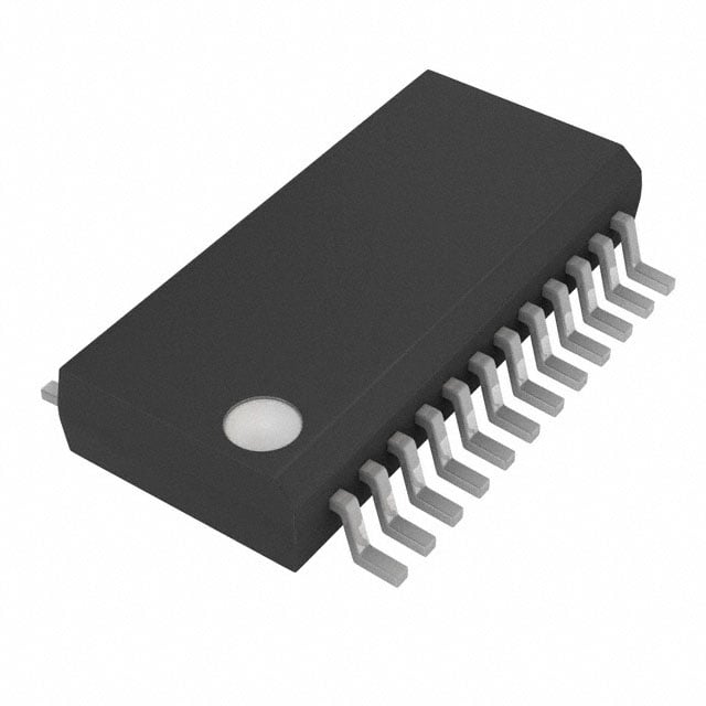
| 封装/外壳 | 24-SSOP(0.154",3.90mm 宽) |
| 封装/箱体 | SSOP-24 |
| 工作温度 | 0°C ~ 70°C |
| 工厂包装数量 | 50 |
| 接口 | 并联 |
| 日期格式 | YY-MM-DD-dd |
| 时间格式 | HH:MM:SS(12/24 小时) |
| 最大工作温度 | + 70 C |
| 最小工作温度 | 0 C |
| 标准包装 | 50 |
| 特性 | 警报器,夏令时,闰年,NVSRAM,方波输出 |
| 电压-电源 | 4.5 V ~ 5.5 V |
| 电压-电源,电池 | 2.5 V ~ 4 V |
| 电流-计时(最大) | 300µA @ 5V |
| 电源电压-最大 | 5.5 V |
| 电源电压-最小 | 4.5 V |
| 类型 | 时钟/日历 |
| 系列 | BQ3285E |


- 商务部:美国ITC正式对集成电路等产品启动337调查
- 曝三星4nm工艺存在良率问题 高通将骁龙8 Gen1或转产台积电
- 太阳诱电将投资9.5亿元在常州建新厂生产MLCC 预计2023年完工
- 英特尔发布欧洲新工厂建设计划 深化IDM 2.0 战略
- 台积电先进制程称霸业界 有大客户加持明年业绩稳了
- 达到5530亿美元!SIA预计今年全球半导体销售额将创下新高
- 英特尔拟将自动驾驶子公司Mobileye上市 估值或超500亿美元
- 三星加码芯片和SET,合并消费电子和移动部门,撤换高东真等 CEO
- 三星电子宣布重大人事变动 还合并消费电子和移动部门
- 海关总署:前11个月进口集成电路产品价值2.52万亿元 增长14.8%


PDF Datasheet 数据手册内容提取
bq3285E/L Real-Time Clock (RTC) Features (cid:228) BCD or binary format for clock General Description and calendar data (cid:228) Direct clock/calendar replace- (cid:228) Calendar in day of the week,day The CMOS bq3285E/L is a low- ment for IBM®AT-compatible of the month,months,and years, power microprocessor peripheral computers and other applications with automatic leap-year adjust- providing a time-of-day clock and ment 100-year calendar with alarm fea- (cid:228) Functionally compatible with the tures and battery operation. The DS1285 (cid:228) Time of day in seconds,minutes, bq3285L supports 3V systems. - Closely matches MC146818A and hours Other bq3285E/L features include pin configuration - 12- or 24-hour format three maskable interrupt sources, (cid:228) 2.7–3.6V operation (bq3285L); - Optional daylight saving soqfugeanree-rwalanveonovuotlpautitl,easntodra2g4e2. bytes 4.5–5.5V operation (bq3285E) adjustment A 32.768kHz output is available for (cid:228) 242 bytes of general nonvolatile (cid:228) Programmable square wave out- sustaining power-management ac- storage put tivities. Wake-up capability is pro- (cid:228) 32.768kHz output for power man- (cid:228) Three individually maskable in- vided by an alarm interrupt, which agement terrupt event flags: isactiveinbattery-backupmode. (cid:228) System wake-up capability— - Periodic rates from 122m s to Thebq3285E/Lwrite-protectsthe alarm interrupt output active in 500ms clock, calendar, and storage registers battery-backup mode - Time-of-day alarm once per during power failure. A backup batterythenmaintainsdataandoper- second to once per day (cid:228) Less than 0.5m A load under bat- atestheclockandcalendar. - tery operation End-of-clock update cycle Thebq3285E/Lisafullycompatible (cid:228) Selectable Intel or Motorola bus (cid:228) 24-pin plastic DIP,SOIC,or real-timeclockforIBMAT-compatible timing SSOP computers and other applications. Theonlyexternalcomponentsarea (cid:228) 14 bytes for clock/calendar and 32.768kHzcrystalandabackupbat- control tery. Pin Connections Pin Names AD0–AD7 Multiplexed address/ RST Reset input data input/output SQW Square wave output MOT 1 24 VCC MOT Bus type select input EXTRAM Extended RAM enable X1 2 23 SQW X2 3 22 EXTRAM CS Chip select input RCL RAM clear input AD0 4 21 RCL AS Address strobe input BC 3V backup cell input AD1 5 20 BC AD2 6 19 INT DS Data strobe input X1–X2 Crystal inputs AD3 7 18 RST AD4 8 17 DS R/W Read/write input VCC Power supply AD5 9 16 VSS INT Interrupt request VSS Ground AD6 10 15 R/W AD7 11 14 AS output VSS 12 13 CS 24-Pin DIP or SOIC/SSOP PN3285E1.eps SLUS004A -DECEMBER 1993 - REVISED MAY 2004 1
bq3285E/L Block Diagram Pin Descriptions AD0–AD7 Multiplexedaddress/datainput/ output MOT Bus type select input The bq3285E/L bus cycle consists of two phases: the address phase and the data- MOTselectsbustimingforeitherMotorola transfer phase. The address phase pre- or Intel architecture. This pin should be cedes the data-transfer phase. During the tiedtoVCCforMotorolatimingortoVSSfor address phase, an address placed on Intel timing (see Table 1). The setting shouldnotbechangedduringsystemopera- AD0–AD7 and EXTRAM is latched into the bq3285E/LonthefallingedgeoftheASsig- tion. MOT is internally pulled low by a nal. During the data-transfer phase of the 30KW resistor. buscycle,theAD0–AD7pinsserveasabidi- rectionaldatabus. Table1.Bus Setup AS Address strobe input Bus MOT DS R/W AS AS serves to demultiplex the address/data Type Level Equivalent Equivalent Equivalent bus. The falling edge of AS latches the ad- DS, E, or dress on AD0–AD7 and EXTRAM. This de- Motorola VCC F 2 R/W AS multiplexing process is independent of the CSsignal. ForDIPandSOICpackageswith RD, WR, MOT=VSS,theASinputisprovidedasignal Intel VSS MEMR, or MEMW, or ALE similartoALEinanIntel-basedsystem. I/OR I/OW 2
bq3285E/L DS Data strobe input EXTRAM Extended RAM enable When MOT = VCC,DS controls data trans- Enables128bytesofadditionalnonvolatile ferduringabq3285E/Lbuscycle. Duringa SRAM. It is connected internally to a 30K readcycle,thebq3285E/Ldrivesthebusaf- W pull-down resistor. To access the RTC ter the rising edge on DS. During a write registers,EXTRAMmustbelow. cycle,thefallingedgeonDSisusedtolatch writedataintothechip. RCL RAM clear input WhenMOT=VSS,theDSinputisprovided AlowlevelontheRCLpincausesthecon- a signal similar to RD, MEMR, or I/OR in tentsofeachofthe242storagebytestobe anIntel-basedsystem. Thefallingedgeon set to FF(hex). The contents of the clock DS is used to enable the outputs during a and control registers are unaffected. This readcycle. pinshouldbeusedasauser-interfaceinput (pushbutton to ground) and not connected R/W Read/writeinput totheoutputofanyactivecomponent. RCL input is only recognized when held low for WhenMOT=VCC,thelevelonR/Widenti- at least 125ms in the presence of VCC.Us- fies the direction of data transfer. A high ing RAM clear does not affect the battery level on R/W indicates a read bus cycle, load. This pin is connected internally to a whereasalowonthispinindicatesawrite 30KW pull-upresistor. buscycle. BC 3V backup cell input When MOT = VSS, R/W is provided a sig- nal similar to WR,MEMW,or I/OW in an BC should be connected to a 3V backup cell Intel-based system. The rising edge on for RTC operation and storage register non- R/Wlatchesdataintothebq3285E/L. volatility in the absence of system power. WhenVCCslewsdownpastVBC(3Vtypical), CS Chip select input the integral control circuitry switches the CS should be driven low and held stable power source to BC. When VCC returns during the data-transfer phase of a bus cy- above VBC, the power source is switched to cleaccessingthebq3285E/L. VCC. Upon power-up, a voltage within the VBC INT Interrupt request output range must be present on the BC pin for theoscillatortostartup. INT is an open-drain output. This allows alarm INT to be valid in battery-backup RST Reset input mode.Tousethisfeature,INTmustbecon- nected to a power supply other than VCC. Thebq3285E/LisresetwhenRSTispulled INT is asserted low when any event flag is low. When reset, INT becomes high imped- set and the corresponding event enable bit ance, and the bq3285E/L is not accessible. is also set. INT becomes high-impedance Table4intheControl/StatusRegisterssec- whenever register C is read (see the Con- tion lists the register bits that are cleared trol/StatusRegisterssection). byareset. SQW Square-wave output Reset may be disabled by connecting RST to VCC. This allows the control bits to re- SQW may output a programmable fre- tain their states through power- quency square-wave signal during normal down/power-upcycles. (VCC valid) system operation. Any one of the 13 specific frequencies may be selected X1–X2 Crystal inputs through register A. This pin is held low when the square-wave enable bit (SQWE) TheX1–X2inputsareprovidedforanexter- in register B is 0 (see the Control/Status nal 32.768kHz quartz crystal,Daiwa DT-26 Registerssection). or equivalent,with 6pF load capacitance.A trimmingcapacitormaybenecessaryforex- A 32.768kHz output is enabled by setting tremelyprecisetime-basegeneration. the SQWE bit in register B to 1 and the 32KE bit in register C to 1 after setting In the absence of a crystal, a 32.768kHz OSC2–OSC0inregisterAto011(binary). waveformcanbefedintotheX1input. 3
bq3285E/L Functional Description darlocationsduringtheupdatecycleattheendofeach update period (see Figure 2). The alarm flag bit may alsobesetduringtheupdatecycle. Address Map Thebq3285E/Lcopiesthelocalregisterupdatesintothe The bq3285E/L provides 14 bytes of clock and con- userbufferaccessedbythehostprocessor. Whena1is trol/statusregistersand242bytesofgeneralnonvolatile writtentotheupdatetransferinhibitbit(UTI)inregis- storage. Figure 1 illustrates the address map for the ter B,the user copy of the clock and calendar bytes re- bq3285E/L. mainsunchanged,whilethelocalcopyofthesamebytes continuestobeupdatedeverysecond. Update Period The update-in-progress bit (UIP) in register A is set tBUC time before the beginning of an update cycle (see Theupdateperiodforthebq3285E/Lisonesecond.The Figure 2). This bit is cleared and the update-complete bq3285E/L updates the contents of the clock and calen- flag(UF)issetattheendoftheupdatecycle. Figure1. Address Map Figure2. Update Period Timing and UIP 4
bq3285E/L Programming the RTC c. Write the appropriate value to the hour format (HF) bit. The time-of-day,alarm,and calendar bytes can be writ- 2. Write new values to all the time,alarm,and tenineithertheBCDorbinaryformat(seeTable2). calendar locations. Thesestepsmaybefollowedtoprogramthetime,alarm, 3. Clear the UTI bit to allow update transfers. andcalendar: Onthenextupdatecycle,theRTCupdatesall10bytes 1. Modify the contents of register B: intheselectedformat. a. Write a 1 to the UTI bit to prevent trans- fers between RTC bytes and user buffer. b. Write the appropriate value to the data format (DF) bit to select BCD or binary format for all time,alarm,and calendar bytes. Table2. Time,Alarm,and Calendar Formats Range Binary-Coded Address RTC Bytes Decimal Binary Decimal 0 Seconds 0–59 00H–3BH 00H–59H 1 Seconds alarm 0–59 00H–3BH 00H–59H 2 Minutes 0–59 00H–3BH 00H–59H 3 Minutes alarm 0–59 00H–3BH 00H–59H 01H–OCH AM; 01H–12H AM; Hours, 12-hour format 1–12 81H–8CH PM 81H–92H PM 4 Hours, 24-hour format 0–23 00H–17H 00H–23H 01H–OCH AM; 01H–12H AM; Hours alarm, 12-hour format 1–12 81H–8CH PM 81H–92H PM 5 Hours alarm, 24-hour format 0–23 00H–17H 00H–23H 6 Day of week (1=Sunday) 1–7 01H–07H 01H–07H 7 Day of month 1–31 01H–1FH 01H–31H 8 Month 1–12 01H–0CH 01H–12H 9 Year 0–99 00H–63H 00H–99H 5
bq3285E/L Square-Wave Output n Thealarminterrupt,programmabletooccuronceper second to once per day, is active in battery-backup mode,providinga“wake-up”feature. The bq3285E/L divides the 32.768kHz oscillator fre- quency to produce the 1Hz update frequency for the n Theupdate-endedinterrupt,whichoccursattheend clockandcalendar. Thirteentapsfromthefrequencydi- ofeachupdatecycle. viderarefedtoa16:1multiplexercircuit. Theoutputof this mux is fed to the SQW output and periodic inter- Eachofthethreeinterrupteventsisenabledbyanindi- ruptgenerationcircuitry. Thefourleast-significantbits vidualinterrupt-enablebitinregisterB. Whenanevent of register A, RS0–RS3, select among the 13 taps (see occurs,itseventflagbitinregisterCisset. Ifthecorre- Table3). Thesquare-waveoutputisenabledbywriting sponding event enable bit is also set,then an interrupt a1tothesquare-waveenablebit(SQWE)inregisterB. request is generated. The interrupt request flag bit A 32.768kHz output may be selected by setting (INTF)ofregisterCissetwitheveryinterruptrequest. OSC2–OSC0 in register A to 011 while SQWE = 1 and Reading register C clears all flag bits, including INTF, 32KE=1. andmakesINThigh-impedance. Twomethodscanbeusedtoprocessbq3285E/Linterrupt Interrupts events: n Enableinterrupteventsandusetheinterruptrequest The bq3285E/L allows three individually selected inter- outputtoinvokeaninterruptserviceroutine. rupt events to generate an interrupt request. These threeinterrupteventsare: n Donotenabletheinterruptsanduseapollingroutine toperiodicallycheckthestatusoftheflagbits. n The periodic interrupt, programmable to occur once every122m sto500ms. Theindividualinterruptsourcesaredescribedindetail inthefollowingsections. Table3.Square-Wave Frequency/Periodic Interrupt Rate Register A Bits Square Wave Periodic Interrupt OSC2 OSC1 OSC0 RS3 RS2 RS1 RS0 Frequency Units Period Units 0 1 0 0 0 0 0 None None 0 1 0 0 0 0 1 256 Hz 3.90625 ms 0 1 0 0 0 1 0 128 Hz 7.8125 ms 0 1 0 0 0 1 1 8.192 kHz 122.070 m s 0 1 0 0 1 0 0 4.096 kHz 244.141 m s 0 1 0 0 1 0 1 2.048 kHz 488.281 m s 0 1 0 0 1 1 0 1.024 kHz 976.5625 m s 0 1 0 0 1 1 1 512 Hz 1.95315 ms 0 1 0 1 0 0 0 256 Hz 3.90625 ms 0 1 0 1 0 0 1 128 Hz 7.8125 ms 0 1 0 1 0 1 0 64 Hz 15.625 ms 0 1 0 1 0 1 1 32 Hz 31.25 ms 0 1 0 1 1 0 0 16 Hz 62.5 ms 0 1 0 1 1 0 1 8 Hz 125 ms 0 1 0 1 1 1 0 4 Hz 250 ms 0 1 0 1 1 1 1 2 Hz 500 ms 32.768 same as above defined 0 1 1 X X X X kHz by RS3–RS0 6
bq3285E/L PeriodicInterrupt UpdateCycleInterrupt The mux output used to drive the SQW output also Theupdatecycleendedflagbit(UF)inregisterCissetto drivestheinterrupt-generationcircuitry. Iftheperiodic a1attheendofanupdatecycle. Iftheupdateinterrupt interrupteventisenabledby writinga1totheperiodic enablebit(UIE)ofregisterBis1,andtheupdatetransfer interruptenablebit(PIE)inregisterC,aninterruptre- inhibitbit(UTI)inregisterBis0,thenaninterruptrequest quest is generated once every 122m s to 500ms. The pe- isgeneratedattheendofeachupdatecycle. riod between interrupts is selected by the same bits in registerAthatselectthesquarewavefrequency(seeTa- Accessing RTC bytes ble3). SettingOSC2–OSC0inregisterAto011doesnot affecttheperiodicinterrupttiming. TheEXTRAMpinmustbelowtoaccesstheRTCregis- AlarmInterrupt ters. Time and calendar bytes read during an update cyclemaybeinerror. Threemethodstoaccessthetime The alarm interrupt is active in battery-backup mode, andcalendarbyteswithoutambiguityare: providing a “wake-up” capability. During each update cycle, the RTC compares the hours, minutes, and sec- n Enable the update interrupt event to generate interruptrequestsattheendoftheupdatecycle. The ondsbyteswiththethreecorrespondingalarmbytes. If interrupt handler has a maximum of 999ms to access amatchofallbytesisfound,thealarminterruptevent theclockbytesbeforethenextupdatecyclebegins(see flagbit,AFinregisterC,issetto1. Ifthealarmevent Figure3). isenabled,aninterruptrequestisgenerated. Analarmbytemayberemovedfromthecomparisonby n Polltheupdate-in-progressbit(UIP)inregisterA. If settingittoa“don’tcare”state. Analarmbyteissetto UIP = 0, the polling routine has a minimum of tBUC timetoaccesstheclockbytes(seeFigure3). a “don’t care” state by writing a 1 to each of its two most-significantbits. A“don’tcare”statemaybeusedto n Use the periodic interrupt event to generate selectthefrequencyofalarminterrupteventsasfollows: interrupt requests every tPI time, such that UIP = 1 always occurs between the periodic interrupts. The n If none of the three alarm bytes is “don’t care,” the frequencyisonceperday,whenhours,minutes,and interrupt handler has a minimum of tPI/2 + tBUC timetoaccesstheclockbytes(seeFigure3). secondsmatch. n If only the hour alarm byte is “don’t care,” the Oscillator Control frequency is once per hour, when minutes and secondsmatch. Whenpowerisfirstappliedtothebq3285E/LandVCCis n If only the hour and minute alarm bytes are “don’t above VPFD,the internal oscillator and frequency divider care,”thefrequencyisonceperminute,whenseconds areturnedonbywritinga010patterntobits4through6 match. ofregisterA.Apatternof011behavesas010butaddition- ally transforms register C into a read/write register. This n If the hour, minute, and second alarm bytes are allowsthe32.768kHzoutputonthesquarewavepintobe “don’tcare,”thefrequencyisoncepersecond. turned on. A pattern of 11X turns the oscillator on, but keepsthefrequencydividerdisabled.Anyotherpatternto thesebitskeepstheoscillatoroff. Figure3. Update-Ended/Periodic Interrupt Relationship 7
bq3285E/L Power-Down/Power-Up Cycle RegisterAprovides: n Statusoftheupdatecycle. The bq3285E and bq3285L power-up/power-down cycles are different. Thebq3285LcontinuouslymonitorsVCCforout-of- RS0–RS3-FrequencySelect tolerance. Duringapowerfailure,whenVCCfallsbelowVPFD (2.53Vtypical),thebq3285Lwrite-protectstheclockandstor- 7 6 5 4 3 2 1 0 ageregisters.ThepowersourceisswitchedtoBCwhenVCCis - - - - RS3 RS2 RS1 RS0 lessthanVPFDandBCisgreaterthanVPFD,orwhenVCCis lessthanVBCandVBCislessthanVPFD. RTCoperationand Thesebitsselectoneofthe13frequenciesfortheSQWout- storage data are sustained by a valid backup energy source. putandtheperiodicinterruptrate,asshowninTable3. When VCC is above VPFD, the power source is VCC. Write- protectioncontinuesfortCSRtimeafterVCCrisesaboveVPFD. OS0–OS2-OscillatorControl Thebq3285EcontinuouslymonitorsVCCforout-of-tolerance. 7 6 5 4 3 2 1 0 During a power failure,when VCC falls below VPFD (4.17V typical), the bq3285E write-protects the clock and storage - OS2 OS1 OS0 - - - - registers. When VCC is below VBC (3V typical),the power sourceisswitchedtoBC. RTCoperationandstoragedata These three bits control the state of the oscillator and aresustainedbyavalidbackupenergysource. WhenVCCis dividerstages. Apatternof010enablesRTCoperation aboveVBC,thepowersourceisVCC.Write-protectioncontin- byturningontheoscillatorandenablingthefrequency uesfortCSRtimeafterVCCrisesaboveVPFD. divider.Apatternof011behavesas010butadditionally transformsregisterCintoaread/writeregister.Thisal- Control/Status Registers lowsthe32.768kHzoutputonthesquarewavepintobe turnedon.Apatternof11Xturnstheoscillatoron,but keepsthefrequencydividerdisabled. When010iswrit- The four control/status registers of the bq3285E/L are ten,theRTCbeginsitsfirstupdateafter500ms. accessible regardless of the status of the update cycle (seeTable4). UIP-UpdateCycleStatus RegisterA 7 6 5 4 3 2 1 0 UIP - - - - - - - Register A Bits 7 6 5 4 3 2 1 0 Thisread-onlybitissetpriortotheupdatecycle. When UIP OS2 OS1 OS0 RS3 RS2 RS1 RS0 UIPequals1,anRTCupdatecyclemaybeinprogress. UIPisclearedattheendofeachupdatecycle. Thisbit is also cleared when the update transfer inhibit (UTI) RegisterAprograms: bitinregisterBis1. n The frequency of the square-wave and the periodic eventrate. n Oscillatoroperation. Table4.Control/Status Registers Bit Name and State on Reset Loc. Reg. (Hex) ReadWrite 7 (MSB) 6 5 4 3 2 1 0 (LSB) A 0A Yes Yes1 UIP na OS2 na OS1 na OS0 na RS3 na RS2 na RS1 na RS0 na B 0B Yes Yes UTI na PIE 0 AIE 0 UIE 0 SQWE 0 DF na HF na DSE na C 0C Yes No2 INTF 0 PF 0 AF 0 UF 0 - 0 32KE na - 0 - 0 D 0D Yes No VRT na - 0 - 0 - 0 - 0 - 0 - 0 - 0 Notes: na = not affected. 1. Except bit 7. 2. Read/write only when OSC2–OSC0 in register A is 011 (binary). 8
bq3285E/L RegisterB SQWE-Square-WaveEnable Register B Bits 7 6 5 4 3 2 1 0 7 6 5 4 3 2 1 0 - - - - SQWE - - - UTI PIE AIE UIE SQWE DF HF DSE Thisbitenablesthesquare-waveoutput: RegisterBenables: 1=Enabled n Updatecycletransferoperation 0=Disabledandheldlow n Square-waveoutput UIE-UpdateCycleInterruptEnable n Interruptevents 7 6 5 4 3 2 1 0 n Daylightsavingadjustment - - - UIE - - - - RegisterBselects: This bit enables an interrupt request due to an update n Clockandcalendardataformats endedinterruptevent: AllbitsofregisterBareread/write. 1=Enabled DSE-DaylightSavingEnable 0=Disabled 7 6 5 4 3 2 1 0 The UIE bit is automatically cleared when the UTI bit - - - - - - - DSE equals1. AIE-AlarmInterruptEnable Thisbitenablesdaylight-savingtimeadjustmentswhen writtento1: 7 6 5 4 3 2 1 0 n On the last Sunday in October, the first time the - - AIE - - - - - bq3285E/L increments past 1:59:59 AM, the time fallsbackto1:00:00AM. This bit enables an interrupt request due to an alarm n On the first Sunday in April, the time springs interruptevent: forwardfrom2:00:00AMto3:00:00AM. 1=Enabled HF-HourFormat 0=Disabled 7 6 5 4 3 2 1 0 PIE-PeriodicInterruptEnable - - - - - - HF - 7 6 5 4 3 2 1 0 - PIE - - - - - - Thisbitselectsthetime-of-dayandalarmhourformat: 1=24-hourformat This bit enables an interrupt request due to a periodic interruptevent: 0=12-hourformat 1=Enabled DF-DataFormat 0=Disabled 7 6 5 4 3 2 1 0 - - - - - DF - - This bit selects the numeric format in which the time, alarm,andcalendarbytesarerepresented: 1=Binary 0=BCD 9
bq3285E/L UTI-UpdateTransferInhibit PF-PeriodicEventFlag 7 6 5 4 3 2 1 0 Thisbitissettoa1everytPItime,wheretPIisthetime periodselectedbythesettingsofRS0–RS3inregisterA. UTI - - - - - - - ReadingregisterCclearsthisbit. 7 6 5 4 3 2 1 0 This bit inhibits the transfer of RTC bytes to the user - PF - - - - - - buffer: 1=InhibitstransferandclearsUIE INTF-InterruptRequestFlag 0=Allowstransfer Thisflagissettoa1whenanyofthefollowingistrue: RegisterC AIE=1andAF=1 RegisterCistheread-onlyeventstatusregister. PIE=1andPF=1 7 6 5 4 3 2 1 0 Register C Bits INTF - - - - - - - 7 6 5 4 3 2 1 0 INTF PF AF UF 0 32KE 0 0 UIE=1andUF=1 ReadingregisterCclearsthisbit. Bits0,1,3-UnusedBits Thesebitsarealwayssetto0. RegisterD RegisterDistheread-onlydataintegritystatusregister. 7 6 5 4 3 2 1 0 - - - - 0 - 0 0 Bits0–6-UnusedBits Thesebitsarealwayssetto0. 32KE-32kHzEnableOutput VRT-ValidRAMandTime This bit may be set to a 1 only when the OSC2–OSC0 Register D Bits bitsinregisterAaresetto011. SettingOSC2–OSC0to 7 6 5 4 3 2 1 0 7 6 5 4 3 2 1 0 VRT 0 0 0 0 0 0 0 - - - - - 32KE - - 1=Validbackupenergysource anythingotherthan011clearsthisbit. IfSQWEinreg- 0=Backupenergysourceisdepleted isterBand32KEareset,a32.768kHzwaveformisout- putonthesquarewavepin. 7 6 5 4 3 2 1 0 UF-UpdateEventFlag - 0 0 0 0 0 0 0 This bit is set to a 1 at the end of the update cycle. When the backup energy source is depleted (VRT = 0), data integrity of the RTC and storage registers is not 7 6 5 4 3 2 1 0 guaranteed. - - - UF - - - - 7 6 5 4 3 2 1 0 VRT - - - - - - - ReadingregisterCclearsthisbit. AF-AlarmEventFlag Thisbitissettoa1whenanalarmeventoccurs.Read- ingregisterCclearsthisbit. 7 6 5 4 3 2 1 0 - - AF - - - - - 10
bq3285E/L Absolute Maximum Ratings—bq3285E Symbol Parameter Value Unit Conditions VCC DC voltage applied on VCCrelative to VSS -0.3 to 7.0 V VT DreCla vtiovleta tgoe V aSpSplied on any pin excluding VCC -0.3 to 7.0 V VT£ VCC+ 0.3 0 to +70°CCommercial TOPR Operating temperature TSTG Storage temperature-55 to +125°C TBIAS Temperature under bias -40 to +85 °C TSOLDER Soldering temperature 260 °C For 10 seconds Note: Permanent device damage may occur ifAbsolute Maximum Ratingsare exceeded.Functional opera- tion should be limited to the Recommended DC Operating Conditions detailed in this data sheet. Expo- sure to conditions beyond the operational limits for extended periods of time may affect device reliability. Absolute Maximum Ratings—bq3285L Symbol Parameter Value Unit Conditions VCC DC voltage applied on VCCrelative to VSS -0.3 to 6.0 V VT DreCla vtiovleta tgoe V aSpSplied on any pin excluding VCC -0.3 to 6.0 V VT£ VCC+ 0.3 TOPR Operating temperature 0 to +70 °C Commercial TSTG Storage temperature -55 to +125 °C TBIAS Temperature under bias -40 to +85 °C TSOLDER Soldering temperature 260 °C For 10 seconds Note: Permanent device damage may occur ifAbsolute Maximum Ratingsare exceeded.Functional opera- tion should be limited to the Recommended DC Operating Conditions detailed in this data sheet. Expo- sure to conditions beyond the operational limits for extended periods of time may affect device reliability. 11
bq3285E/L Recommended DC Operating Conditions—bq3285E (T = T ) A OPR Symbol Parameter Minimum Typical Maximum Unit VCC Supply voltage 4.5 5.0 5.5 V VSS Supply voltage 0 0 0 V VIL Input low voltage -0.3 - 0.8 V VIH Input high voltage 2.2 - VCC+ 0.3 V VBC Backup cell voltage 2.5 - 4.0 V Note: Typical values indicate operation at TA= 25°C. Recommended DC Operating Conditions—bq3285L (T = T ) A OPR Symbol Parameter Minimum Typical Maximum Unit VCC Supply voltage 2.7 3.15 3.6 V VSS Supply voltage 0 0 0 V VIL Input low voltage -0.3 - 0.6 V VIH Input high voltage 2.2 - VCC+ 0.3 V VBC Backup cell voltage 2.4 - 4.0 V Note: Typical values indicate operation at TA= 25°C. Crystal Specifications—bq3285E/L (DT-26 or Equivalent) Symbol Parameter Minimum Typical Maximum Unit fO Oscillation frequency - 32.768 - kHz CL Load capacitance - 6 - pF TP Temperature turnover point 20 25 30 °C k Parabolic curvature constant - - -0.042 ppm/°C Q Quality factor 40,000 70,000 - R1 Series resistance - - 45 KW C0 Shunt capacitance - 1.1 1.8 pF C0/C1 Capacitance ratio - 430 600 DL Drive level - - 1 m W D f/fO Aging (first year at 25°C) - 1 - ppm 12
bq3285E/L DC Electrical Characteristics—bq3285E (T = T ,V = 5V– 10%) A OPR CC Symbol Parameter Minimum Typical Maximum Unit Conditions/Notes ILI Input leakage current - - – 1 m A VIN= VSSto VCC AD0–AD7,INT,and SQW ILO Output leakage current - - – 1 m A in high impedance, VOUT= VSSto VCC VOH Output high voltage 2.4 - - V IOH= -2.0 mA VOL Output low voltage - - 0.4 V IOL= 4.0 mA Min.cycle,duty = 100%, ICC Operating supply current - 7 15 mA IOH= 0mA,IOL= 0mA ICCSB Standby supply current - 300 - m A CVSIN‡=V VCSCS-o 0r .V2CC, VSO Supply switch-over voltage - VBC - V ICCB Battery operation current - 0.3 0.5 m A VBC= 3V,TA= 25°C VPFD Power-fail-detect voltage 4.0 4.17 4.35 V IRCL Input current whenRCL= VSS. - - 185 m A Internal 30K pull-up Input current when MOT = VCC - - -185 m A Internal 30K pull-down IMOTH Input current when MOT = VSS - - 0 m A Internal 30K pull-down InputcurrentwhenEXTRAM= - - -185 m A Internal 30K pull-down VCC IXTRAM InputcurrentwhenEXTRAM= - - 0 m A Internal 30K pull-down VSS Note: Typical values indicate operation at TA= 25°C,VCC= 5V or VBC= 3V. 13
bq3285E/L DC Electrical Characteristics—bq3285L (T = T ,V = 3.15V– 0.45V) A OPR CC Symbol Parameter Minimum Typical Maximum Unit Conditions/Notes ILI Input leakage current - - – 1 m A VIN= VSSto VCC AD0–AD7and INT in high ILO Output leakage current - - – 1 m A impedance, VOUT= VSSto VCC VOH Output high voltage 2.2 - - V IOH= -1.0 mA VOL Output low voltage - - 0.4 V IOL= 2.0 mA Min.cycle,duty = 100%,I ICC Operating supply current - 5 9 mA OH = 0mA,IOL= 0mA ICCSB Standby supply current - 100 - m A CVSIN‡=V VCSCS-o 0r .V2CC, - VPFD - V VBC> VPFD VSO Supply switch-over voltage - VBC - V VBC< VPFD ICCB Battery operation current - 0.3 0.5 m A VVBCCC=< 3VVB,CTA= 25°C, VPFD Power-fail-detect voltage 2.4 2.53 2.65 V IRCL Input current whenRCL= VSS. - - 120 m A Internal 30K pull-up Input current when MOT = VCC - - -120 m A Internal 30K pull-down IMOTH Input current when MOT = VSS - - 0 m A Internal 30K pull-down Input current when EXTRAM = - - -120 m A Internal 30K pull-down VCC IXTRAM Input current when EXTRAM = - - 0 m A Internal 30K pull-down VSS Note: Typical values indicate operation at TA= 25°C,VCC= 3V. 14
bq3285E/L Capacitance—bq3285E/L (T = 25°C, F = 1MHz, V = 5.0V) A CC Symbol Parameter Minimum Typical Maximum Unit Conditions CI/O Input/output capacitance - - 7 pF VOUT= 0V CIN Input capacitance - - 5 pF VIN= 0V Note: This parameter is sampled and not 100% tested. It does not include the X1 or X2 pin. AC Test Conditions—bq3285E Parameter Test Conditions Input pulse levels 0 to 3.0 V Input rise and fall times 5 ns Input and output timing reference levels 1.5 V (unless otherwise specified) Output load (including scope and jig) See Figures 4 and 5 Figure 4. Output Load A—bq3285E Figure 5.Output Load B—bq3285E 15
bq3285E/L AC Test Conditions—bq3285L Parameter Test Conditions Input pulse levels 0 to 2.3 V Input rise and fall times 5 ns Input and output timing reference levels 1.2 V (unless otherwise specified) Output load (including scope and jig) See Figures 6 and 7 Figure 6.Output Load A—bq3285L Figure 7.Output Load B—bq3285L 16
bq3285E/L Read/Write Timing—bq3285E (T = T ,V = 5V– 10%) A OPR CC Symbol Parameter Minimum Typical Maximum Unit Notes tCYC Cycle time 160 - - ns tDSL DS low orRD/WRhigh time 80 - - ns tDSH DS high orRD/WRlow time 55 - - ns tRWH R/Whold time 0 - - ns tRWS R/Wsetup time 10 - - ns tCS Chip select setup time 5 - - ns tCH Chip select hold time 0 - - ns tDHR Read data hold time 0 - 25 ns tDHW Write data hold time 0 - - ns tAS Address setup time 20 - - ns tAH Address hold time 5 - - ns tDAS Delay time,DS to AS rise 10 - - ns tASW Pulse width,AS high 30 - - ns Delay time,AS to DS rise (RD/WR tASD fall) 35 - - ns Output data delay time from DS rise tOD (RDfall) - - 50 ns tDW Write data setup time 30 - - ns tBUC Delay time before update cycle - 244 - m s tPI Periodic interrupt time interval - - - - See Table 3 tUC Time of update cycle - 1 - m s 17
bq3285E/L Read/Write Timing—bq3285L (T = T ,V = 3.15V– 0.45V) A OPR CC Symbol Parameter Minimum Typical Maximum Unit Notes tCYC Cycle time 270 - - ns tDSL DS low orRD/WRhigh time 135 - - ns tDSH DS high orRD/WRlow time 90 - - ns tRWH R/Whold time 0 - - ns tRWS R/Wsetup time 15 - - ns tCS Chip select setup time 8 - - ns tCH Chip select hold time 0 - - ns tDHR Read data hold time 0 - 40 ns tDHW Write data hold time 0 - - ns tAS Address setup time 30 - - ns tAH Address hold time 15 - - ns tDAS Delay time,DS to AS rise 15 - - ns tASW Pulse width,AS high 50 - - ns Delay time,AS to DS rise (RD/WR tASD fall) 55 - - ns Output data delay time from DS rise tOD (RDfall) - - 100 ns tDW Write data setup time 50 - - ns tBUC Delay time before update cycle - 244 - m s tPI Periodic interrupt time interval - - - - See Table 3 tUC Time of update cycle - 1 - m s 18
bq3285E/L Motorola Bus Read/Write Timing—bq3285E/L 19
bq3285E/L Intel Bus Read Timing—bq3285E/L Intel Bus Write Timing—bq3285E/L 20
bq3285E/L Power-Down/Power-Up Timing—bq3285E (T = T ) A OPR Symbol Parameter Minimum Typical Maximum Unit Conditions tF VCCslew from 4.5V to 0V 300 - - m s tR VCCslew from 0V to 4.5V 100 - - m s Internal write-protection tCSR CSat VIHafter power-up 20 - 200 ms period after VCCpasses VPFD on power-up. Caution: Negative undershoots below the absolute maximum rating of -0.3V in battery-backup mode may affect data integrity. Power-Down/Power-Up Timing—bq3285E 21
bq3285E/L Power-Down/Power-Up Timing—bq3285L (T = T ) A OPR Symbol Parameter Minimum Typical Maximum Unit Conditions tF VCCslew from 2.7V to 0V 300 - - m s tR VCCslew from 0V to 2.7V 100 - - m s Internal write-protection tCSR CSat VIHafter power-up 20 - 200 ms period after VCCpasses VPFD on power-up. Caution: Negative undershoots below the absolute maximum rating of -0.3V in battery-backup mode may affect data integrity. Power-Down/Power-Up Timing—bq3285L 22
bq3285E/L Interrupt Delay Timing—bq3285E/L (T = T ) A OPR Symbol Parameter Minimum Typical Maximum Unit tRSW Reset pulse width 5 - - m s tIRR INTrelease fromRST - - 2 m s tIRD INTrelease from DS - - 2 m s Interrupt Delay Timing—bq3285E/L 23
bq3285E/L 24-Pin DIP (P) 24-Pin DIP(0.600" DIP) Inches Millimeters Dimension Min. Max. Min. Max. A 0.160 0.190 4.06 4.83 A1 0.015 0.040 0.38 1.02 B 0.015 0.022 0.38 0.56 B1 0.045 0.065 1.14 1.65 C 0.008 0.013 0.20 0.33 D 1.240 1.280 31.50 32.51 E 0.600 0.625 15.24 15.88 E1 0.530 0.570 13.46 14.48 e 0.600 0.670 15.24 17.02 G 0.090 0.110 2.29 2.79 L 0.115 0.150 2.92 3.81 S 0.070 0.090 1.78 2.29 24-Pin SOIC (S) 24-Pin S(0.300" SOIC) Inches Millimeters Dimension Min. Max. Min. Max. B e A 0.095 0.105 2.41 2.67 D A1 0.004 0.012 0.10 0.30 B 0.013 0.020 0.33 0.51 C 0.008 0.013 0.20 0.33 D 0.600 0.615 15.24 15.62 E 0.290 0.305 7.37 7.75 E e 0.045 0.055 1.14 1.40 H H 0.395 0.415 10.03 10.54 A C L 0.020 0.040 0.51 1.02 .004 A1 L 24
bq3285E/L 24-Pin SSOP (SS) 24-Pin SS(0.150" SSOP) Inches Millimeters Dimension Min. Max. Min. Max. A 0.061 0.068 1.55 1.73 A1 0.004 0.010 0.10 0.25 B 0.008 0.012 0.20 0.30 C 0.007 0.010 0.18 0.25 D 0.337 0.344 8.56 8.74 E 0.150 0.157 3.81 3.99 e .025 BSC 0.64 BSC H 0.230 0.244 5.84 6.20 L 0.016 0.035 0.41 0.89 25
bq3285E/L Data Sheet Revision History Change Page Description Nature of Change No. No. 1 8 Register C, bit 2 Was 0; is na (not affected) 1 18 Output data delay time tOD Was 80 ns max; is 100 ns max 2 1, 24, 26 Package option change Lst time buy for some package options. 3 1, 24, 26 Package option change Removed PLCC and added industrial SSOP package options 4 1, 11 Package option change Industrial package option removed Note: Change 1 = Jan. 1995 B “Final” changes from Dec. 1993 A “Preliminary”. Change 2 = Jan. 1999 C changes from Jan. 1995 B Change 3 = Apr. 1999 D changes from Jan. 1999 C. Change 4 = May 2004 (SLUS004A) changes from Apr. 1999 D 26
bq3285E/L Ordering Information bq3285E/L - Temperature: blank=Commercial(0to+70°C) PackageOption: P=24-pinplasticDIP(0.600) S=24-pinSOIC(0.300) SS=24-pinSSOP(0.150) Device: bq3285EReal-TimeClockwith242 bytesofgeneralstorage or bq3285LReal-TimeClockwith242 bytesofgeneralstorage (3Voperation) bq3285L onlyavailablein24-pinSSOP(0.150). 27
IMPORTANT NOTICE Texas Instruments Incorporated and its subsidiaries (TI) reserve the right to make corrections, modifications, enhancements, improvements, and other changes to its products and services at any time and to discontinue any product or service without notice. Customers should obtain the latest relevant information before placing orders and should verify that such information is current and complete. All products are sold subject to TI’s terms and conditions of sale supplied at the time of order acknowledgment. TI warrants performance of its hardware products to the specifications applicable at the time of sale in accordance with TI’s standard warranty. Testing and other quality control techniques are used to the extent TI deems necessary to support this warranty. Except where mandated by government requirements, testing of all parameters of each product is not necessarily performed. TI assumes no liability for applications assistance or customer product design. Customers are responsible for their products and applications using TI components. To minimize the risks associated with customer products and applications, customers should provide adequate design and operating safeguards. TI does not warrant or represent that any license, either express or implied, is granted under any TI patent right, copyright, mask work right, or other TI intellectual property right relating to any combination, machine, or process in which TI products or services are used. Information published by TI regarding third-party products or services does not constitute a license from TI to use such products or services or a warranty or endorsement thereof. Use of such information may require a license from a third party under the patents or other intellectual property of the third party, or a license from TI under the patents or other intellectual property of TI. Reproduction of information in TI data books or data sheets is permissible only if reproduction is without alteration and is accompanied by all associated warranties, conditions, limitations, and notices. Reproduction of this information with alteration is an unfair and deceptive business practice. TI is not responsible or liable for such altered documentation. Resale of TI products or services with statements different from or beyond the parameters stated by TI for that product or service voids all express and any implied warranties for the associated TI product or service and is an unfair and deceptive business practice. TI is not responsible or liable for any such statements. Following are URLs where you can obtain information on other Texas Instruments products and application solutions: Products Applications Amplifiers amplifier.ti.com Audio www.ti.com/audio Data Converters dataconverter.ti.com Automotive www.ti.com/automotive DSP dsp.ti.com Broadband www.ti.com/broadband Interface interface.ti.com Digital Control www.ti.com/digitalcontrol Logic logic.ti.com Military www.ti.com/military Power Mgmt power.ti.com Optical Networking www.ti.com/opticalnetwork Microcontrollers microcontroller.ti.com Security www.ti.com/security Telephony www.ti.com/telephony Video & Imaging www.ti.com/video Wireless www.ti.com/wireless Mailing Address: Texas Instruments Post Office Box 655303 Dallas, Texas 75265 Copyright 2004, Texas Instruments Incorporated