ICGOO在线商城 > 集成电路(IC) > PMIC - 电池管理 > BQ24315DSGR
 Datasheet下载
- 型号: BQ24315DSGR
- 制造商: Texas Instruments
- 库位|库存: xxxx|xxxx
- 要求:
| 数量阶梯 | 香港交货 | 国内含税 |
| +xxxx | $xxxx | ¥xxxx |
查看当月历史价格
查看今年历史价格
BQ24315DSGR产品简介:
ICGOO电子元器件商城为您提供BQ24315DSGR由Texas Instruments设计生产,在icgoo商城现货销售,并且可以通过原厂、代理商等渠道进行代购。 BQ24315DSGR价格参考。Texas InstrumentsBQ24315DSGR封装/规格:PMIC - 电池管理, Battery Battery Protection IC Lithium-Ion 8-WSON (2x2)。您可以下载BQ24315DSGR参考资料、Datasheet数据手册功能说明书,资料中有BQ24315DSGR 详细功能的应用电路图电压和使用方法及教程。
BQ24315DSGR 是德州仪器(Texas Instruments)推出的一款高度集成的电源管理IC(PMIC),主要用于电池管理领域。该型号特别适用于便携式设备中的单节锂离子或锂聚合物电池充电管理。以下是其典型应用场景:

 1. 智能手机和平板电脑
   - BQ24315DSGR 支持高效的开关模式充电,能够为智能手机和平板电脑提供快速、稳定的充电功能。
   - 它具有输入电流调节功能,可以防止适配器过载,同时支持USB On-The-Go (OTG) 功能,允许设备在需要时作为电源输出。

 2. 可穿戴设备
   - 如智能手表、健身追踪器等小型设备,对体积和功耗要求较高。BQ24315DSGR 的小尺寸封装(DSG 封装)和低静态电流特性使其非常适合这些应用。
   - 其高效率的充电电路可延长设备的续航时间。

 3. 蓝牙音箱和其他便携式音频设备
   - 这些设备通常需要在紧凑的空间内实现高效充电和放电管理。BQ24315DSGR 提供了灵活的充电配置,并支持输入电压范围较宽的适配器或USB端口。

 4. 物联网(IoT)设备
   - 包括智能家居设备、环境监测传感器等,这些设备通常依赖电池供电并需要长时间运行。BQ24315DSGR 的精准充电控制和保护功能确保了电池的安全性和寿命。

 5. 手持式医疗设备
   - 如血糖仪、脉搏血氧仪等,这类设备对可靠性和安全性要求极高。BQ24315DSGR 提供了过压、过流、过温等多种保护机制,保障设备在各种条件下的正常工作。

 6. 便携式电源银行(移动电源)
   - BQ24315DSGR 的双向降压/升压架构支持高效能量转换,非常适合用于移动电源的设计。它还可以通过I2C接口实现复杂的系统监控和控制。

 核心优势:
- 集成度高:减少了外部元件数量,降低了PCB面积需求。
- 精确充电:支持恒流/恒压(CC/CV)充电模式,充电精度高。
- 安全性强:内置多重保护功能,如电池温度检测、短路保护等。
- 灵活性好:可通过引脚或软件配置调整充电参数,适应不同设计需求。

综上所述,BQ24315DSGR 广泛应用于需要高效、安全、紧凑电池管理方案的各种便携式电子设备中。
| 参数 | 数值 |
| 产品目录 | 集成电路 (IC)半导体 |
| 描述 | IC LI+ CHARGER FRONT END 8-SON电池管理 Overvltg & Overcrnt Protection IC |
| 产品分类 | |
| 品牌 | Texas Instruments |
| 产品手册 | http://www.ti.com/litv/slus817a |
| 产品图片 |
|
| rohs | 符合RoHS无铅 / 符合限制有害物质指令(RoHS)规范要求 |
| 产品系列 | 电源管理 IC,电池管理,Texas Instruments BQ24315DSGR- |
| 数据手册 | |
| 产品型号 | BQ24315DSGR |
| PCN组件/产地 | |
| 产品目录页面 | |
| 产品种类 | 电池管理 |
| 产品类型 | Charge Management |
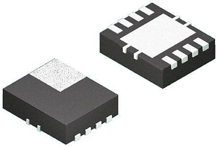
| 供应商器件封装 | 8-WSON (2x2) |
| 其它名称 | 296-23341-6 |
| 功能 | 过压/欠压保护 |
| 包装 | Digi-Reel® |
| 单位重量 | 11 mg |
| 商标 | Texas Instruments |
| 安装类型 | 表面贴装 |
| 安装风格 | SMD/SMT |
| 封装 | Reel |
| 封装/外壳 | 8-WFDFN 裸露焊盘 |
| 封装/箱体 | WSON-8 |
| 工作温度 | -40°C ~ 125°C |
| 工作电源电压 | 30 V |
| 工厂包装数量 | 3000 |
| 最大工作温度 | + 125 C |
| 最小工作温度 | - 40 C |
| 标准包装 | 1 |
| 电压-电源 | 3.3 V ~ 30 V |
| 电池化学 | 锂离子 |
| 电池类型 | Li-Ion |
| 系列 | BQ24315 |
| 输出电压 | 5.5 V |
| 输出电流 | 2 A |
| 配用 | /product-detail/zh/BQ24315EVM/296-30767-ND/1896141 |


- 商务部:美国ITC正式对集成电路等产品启动337调查
- 曝三星4nm工艺存在良率问题 高通将骁龙8 Gen1或转产台积电
- 太阳诱电将投资9.5亿元在常州建新厂生产MLCC 预计2023年完工
- 英特尔发布欧洲新工厂建设计划 深化IDM 2.0 战略
- 台积电先进制程称霸业界 有大客户加持明年业绩稳了
- 达到5530亿美元!SIA预计今年全球半导体销售额将创下新高
- 英特尔拟将自动驾驶子公司Mobileye上市 估值或超500亿美元
- 三星加码芯片和SET,合并消费电子和移动部门,撤换高东真等 CEO
- 三星电子宣布重大人事变动 还合并消费电子和移动部门
- 海关总署:前11个月进口集成电路产品价值2.52万亿元 增长14.8%


PDF Datasheet 数据手册内容提取
bq24313 bq24315 www.ti.com............................................................................................................................................... SLUS817A–MARCH2008–REVISEDNOVEMBER2008 OVERVOLTAGE AND OVERCURRENT PROTECTION IC AND Li+ CHARGER FRONT-END PROTECTION IC FEATURES • 5.5VLDOModeVoltageRegulation 1 • ProvidesProtectionforThreeVariables: • AvailableinSpace-SavingSmall8Lead2mm 23 – InputOvervoltage,withRapidResponsein ×2mmSON <1m s APPLICATIONS – User-ProgrammableOvercurrentwith • MobilePhonesandSmartPhones CurrentLimiting • PDAs – BatteryOvervoltage • MP3Players • 30VMaximumInputVoltage • Low-PowerHandheldDevices • Supportsupto1.5AInputCurrent • Bluetooth™Headsets • RobustAgainstFalseTriggeringDueto CurrentTransients • ThermalShutdown • EnableInput • StatusIndication–FaultCondition DESCRIPTION The bq24313 and bq24315 are highly integrated circuits designed to provide protection to Li-ion batteries from failures of the charging circuit. The IC continuously monitors the input voltage, the input current, and the battery voltage. The output acts as a linear regulator. The output is regulated to V for inputs between V and O(REG) O(REG) the overvoltage threshold. If an input overvoltage condition occurs, the IC immediately removes power from the charging circuit by turning off an internal switch. In the case of an overcurrent condition, it limits the system current at the threshold value, and if the overcurrent persists, switches the pass element OFF after a blanking period. Additionally, the IC also monitors its own die temperature and switches off if it exceeds 140°C. The input overcurrentthresholdisuser-programmable. TheICcanbecontrolledbyaprocessorandalsoprovidesstatusinformationaboutfaultconditionstothehost. APPLICATION SCHEMATIC ACAdapter VDC 1 IN OUT 8 1mF 1mF GND bq24080 bq24313 Charger IC bq24315 SYSTEM VBAT 6 FAULT 4 CE 5 S M VS ILI 2 7 1 Pleasebeawarethatanimportantnoticeconcerningavailability,standardwarranty,anduseincriticalapplicationsofTexas Instrumentssemiconductorproductsanddisclaimerstheretoappearsattheendofthisdatasheet. PowerPADisatrademarkofTexasInstruments. 2 BluetoothisatrademarkofBluetoothSIG,Inc. 3 PRODUCTIONDATAinformationiscurrentasofpublicationdate. Copyright©2008,TexasInstrumentsIncorporated Products conform to specifications per the terms of the Texas Instruments standard warranty. Production processing does not necessarilyincludetestingofallparameters.
bq24313 bq24315 SLUS817A–MARCH2008–REVISEDNOVEMBER2008............................................................................................................................................... www.ti.com Thesedeviceshavelimitedbuilt-inESDprotection.Theleadsshouldbeshortedtogetherorthedeviceplacedinconductivefoam duringstorageorhandlingtopreventelectrostaticdamagetotheMOSgates. ORDERINGINFORMATION(1) DEVICE(2) OVPTHRESHOLD PACKAGE MARKING bq24313DSG 10.5V 2mmx2mmSON NXQ bq24315DSG 5.85V 2mmx2mmSON CGM (1) Forthemostcurrentpackageandorderinginformation,seethePackageOptionAddendumattheend ofthisdocument,orseetheTIwebsiteatwww.ti.com. (2) Toordera3000piecereeladdRtothepartnumber,ortoordera250piecereeladdTtothepart number. PACKAGE DISSIPATION RATINGS DESIGNATOR PACKAGE Rq JC Rq JA DSG 2×2SON 5°C/W 75°C/W ABSOLUTE MAXIMUM RATINGS(1) overoperatingfree-airtemperaturerange(unlessotherwisenoted) PARAMETER PIN VALUE UNIT IN(withrespecttoVSS) –0.3to30 V Inputvoltage OUT(withrespecttoVSS) –0.3to12 V I ILIM,FAULT,CE,VBAT(withrespecttoVSS) –0.3to7 I Inputcurrent IN 2 A I I Outputcurrent OUT 2 A O Outputsinkcurrent FAULT 15 mA All(HumanBodyModelperJESD22-A114-E) 2000 V All(MachineModelperJESD22-A115-E) 200 V ESD WithstandVoltage All(ChargeDeviceModelperJESD22-C101-C) 500 V IN(IEC61000-4-2)(withINbypassedtotheVSS 15(AirDischarge) kV witha1-m Flow-ESRceramiccapacitor) 8(Contact) T Junctiontemperature –40to150 °C J T Storagetemperature –65to150 °C stg (1) Stressesbeyondthoselistedunderabsolutemaximumratingsmaycausepermanentdamagetothedevice.Thesearestressratings only,andfunctionaloperationofthedeviceattheseoranyotherconditionsbeyondthoseindicatedunderrecommendedoperating conditionsisnotimplied.Exposuretoabsolute-maximum-ratedconditionsforextendedperiodsmayaffectdevicereliability.Allvoltage valuesarewithrespecttothenetworkgroundterminalunlessotherwisenoted. RECOMMENDED OPERATING CONDITIONS overoperatingfree-airtemperaturerange(unlessotherwisenoted) MIN MAX UNIT V Inputvoltagerange 3.3 30 V IN I Inputcurrent,INpin 1.5 A IN I Outputcurrent,OUTpin 1.5 A OUT R OCPProgrammingresistor 15 90 kΩ (ILIM) T Junctiontemperature –40 125 °C J 2 SubmitDocumentationFeedback Copyright©2008,TexasInstrumentsIncorporated ProductFolderLink(s):bq24313bq24315
bq24313 bq24315 www.ti.com............................................................................................................................................... SLUS817A–MARCH2008–REVISEDNOVEMBER2008 ELECTRICAL CHARACTERISTICS overjunctiontemperaturerange–40°Cto125°Candrecommendedsupplyvoltage(unlessotherwisenoted) PARAMETER TESTCONDITIONS MIN TYP MAX UNIT IN Undervoltagelock-out,inputpower UVLO CE=Low,V increasingfrom0Vto3V 2.6 2.7 2.8 V detectedthreshold IN V HysteresisonUVLO CE=Low,V decreasingfrom3Vto0V 200 260 300 mV hys(UVLO) IN Deglitchtime,inputpowerdetected CE=Low.TimemeasuredfromV 0V→5V1m s t IN 8 ms DGL(PGOOD) status rise-time,tooutputturningON I Operatingcurrent CE=Low,NoloadonOUTpin, 400 600 m A DD V =5V,R =25kΩ IN (ILIM) I Standbycurrent CE=High,V =5V 65 95 m A STDBY IN INPUTTOOUTPUTCHARACTERISTICS V Drop-outvoltageINtoOUT CE=Low,V =5V,I =1A 170 280 mV DO IN OUT OUPUTVOLTAGEREGULATION V Outputvoltage CE=Low,V =6.5V,I = bq24313 5.67 5.85 6.03 V O(REG) IN OUT 1A CE=Low,V =5.7V,I = bq24315 5.3 5.5 5.7 IN OUT 1A INPUTOVERVOLTAGEPROTECTION CE=Low,V increasing bq24313 10.2 10.5 10.8 V Inputovervoltageprotectionthreshold IN V OVP from5Vto11V bq24315 5.71 5.85 6.00 t InputOVpropagationdelay(1) CE=Low 200 ns PD(OVP) HysteresisonOVP CE=Low,V decreasing bq24313 60 120 180 IN Vhys(OVP) from11Vto5V mV bq24315 20 60 110 Recoverytimefrominputovervoltage CE=Low,Timemeasuredfrom tON(OVP) condition V 7.5V→5V,1m sfall-time 8 ms IN INPUTOVERCURRENTPROTECTION Inputovercurrentprotectionthreshold I 300 1500 mA OCP range CE=Low,R =24.9kΩ, I Inputovercurrentprotectionthreshold (ILIM) 900 1000 1100 mA OCP 3V≤V <V –V IN OVP hys(OVP) Adjustablecurrentlimitfactor A= K 25 (ILIM) kΩ t Blankingtime,inputovercurrent 176 m s BLANK(OCP) detected Recoverytimefrominputovercurrent t 64 ms REC(OCP) condition BATTERYOVERVOLTAGEPROTECTION Batteryovervoltageprotection BV CE=Low,V >4.4V 4.30 4.35 4.4 V OVP threshold IN V HysteresisonBV CE=Low,V >4.4V 200 275 320 mV hys(Bovp) OVP IN I InputbiascurrentonVBATpin V =4.4V,T =25°C 10 nA (VBAT) (VBAT) J t Deglitchtime,batteryovervoltage CE=Low,VIN>4.4V.TimemeasuredfromV(VBAT) 176 m s DGL(Bovp) detected risingfrom4.1Vto4.4VtoFAULTgoinglow. THERMALPROTECTION T Thermalshutdowntemperature 140 150 °C J(OFF) T Thermalshutdownhysteresis 20 °C J(OFF-HYS) LOGICLEVELSONCE V Low-levelinputvoltage 0 0.4 V IL V High-levelinputvoltage 1.4 V IH I Low-levelinputcurrent V =0V 1 m A IL (/CE) (1) Nottestedinproduction.Specifiedbydesign. Copyright©2008,TexasInstrumentsIncorporated SubmitDocumentationFeedback 3 ProductFolderLink(s):bq24313bq24315
bq24313 bq24315 SLUS817A–MARCH2008–REVISEDNOVEMBER2008............................................................................................................................................... www.ti.com ELECTRICAL CHARACTERISTICS (continued) overjunctiontemperaturerange–40°Cto125°Candrecommendedsupplyvoltage(unlessotherwisenoted) PARAMETER TESTCONDITIONS MIN TYP MAX UNIT I High-levelinputcurrent V =1.8V 15 m A IH (/CE) LOGICLEVELSONFAULT V Outputlowvoltage I =5mA 0.2 V OL SINK I Leakagecurrent,FAULTpinHI-Z V =5V 10 m A lkg (/FAULT) 4 SubmitDocumentationFeedback Copyright©2008,TexasInstrumentsIncorporated ProductFolderLink(s):bq24313bq24315
bq24313 bq24315 www.ti.com............................................................................................................................................... SLUS817A–MARCH2008–REVISEDNOVEMBER2008 Q1 IN OUT Charge Pump Bandgap Bias Gen VBG V ISNS ILIM V BG ILIMREF Current limiting V loop O(REG) Loop OFF OCPComparator FAULT ILIMREF-Δ t BLANK(OCP) V ISNS V IN COUNTERS, V CONTROL, BG OVP AND STATUS CE t DGL(PGOOD) VBAT V IN V BG V UVLO BG THERMAL tDGL(BOVP) SHUTDOWN VSS Figure1.SimplifiedBlockDiagram Copyright©2008,TexasInstrumentsIncorporated SubmitDocumentationFeedback 5 ProductFolderLink(s):bq24313bq24315
bq24313 bq24315 SLUS817A–MARCH2008–REVISEDNOVEMBER2008............................................................................................................................................... www.ti.com TERMINAL FUNCTIONS TERMINAL I/O DESCRIPTION NAME DSG Inputpower.ConnectINtotheexternalDCsupply.BypassINtoVSSwitha1m Fceramiccapacitor IN 1 I (minimum). VSS 2 – Groundterminal Thispinmayhaveinternalcircuitsusedfortestpurposes.Donotmakeanyexternalconnectiontothis NC 3 pinfornormaloperation. Open-drain,devicestatusoutput.FAULT=LowindicatesthattheinputFETQ1isoffduetoinput FAULT 4 O overvoltage,inputovercurrent,batteryovervoltage,orthermalshutdown.FAULTishighimpedance duringnormaloperation.ConnectapullupresistorfromFAULTtothedesiredlogiclevelvoltagerail. 5 I Chipenableactivelowinput.ConnectCE=HightodisabletheICandturntheinputFEToff.Connect CE CE=lowfornormaloperation.CEisinternallypulleddown. VBAT 6 I Batteryvoltagesenseinput.Connecttothebatterypackpositiveterminalthrougharesistor. Inputovercurrentthresholdprogramming.ConnectaresistorfromILIMtoVSStosettheovercurrent ILIM 7 I/O threshold. 8 O Outputterminaltothechargingsystem.ConnectOUTtotheexternalloadcircuitry.BypassOUTtoVSS OUT witha1m Fceramiccapacitor(minimum). ThereisaninternalelectricalconnectionbetweentheexposedthermalpadandtheVSSpinofthe device.ThethermalpadmustbeconnectedtothesamepotentialastheVSSpinontheprintedcircuit ThermalPAD – board.Donotusethethermalpadastheprimarygroundinputforthedevice.TheVSSpinmustbe connectedtogroundatalltimes. DSGPackage (TopView) IN 1 8 OUT VSS 2 7 ILIM bq24313 bq24315 NC 3 6 VBAT FAULT 4 5 CE 6 SubmitDocumentationFeedback Copyright©2008,TexasInstrumentsIncorporated ProductFolderLink(s):bq24313bq24315
bq24313 bq24315 www.ti.com............................................................................................................................................... SLUS817A–MARCH2008–REVISEDNOVEMBER2008 TYPICAL OPERATING PERFORMANCE Test conditions (unless otherwise noted) for typical operating performance: V = 5 V, C = 1 m F, C = 1 m F, IN IN OUT R =25kΩ,R =100kΩ,T =25°C,V =3.3V(seeFigure22fortheTypicalApplicationCircuit) (ILIM) BAT A PU NORMALPOWER-ONSHOWINGSOFT-START OVPATPOWER-ON ROUT= 6.6W VIN= 0 V to 9 V, tr= 50ms V 2 V/div IN 5 V/div V IN 2 V/div VOUT 200 mV/div VOUT 200 mA/div IIN 200 mA/div IIN t - Time - 2 ms/div t - Time - 2 ms/div Figure2. Figure3. OVPRESPONSEFORINPUTSTEP OVPRESPONSEFORINPUTSTEP VIN= 5 V to 12 V step VIN= 5 V to 12 V, tr= 20ms 5 V/div VIN 5 V/div VIN 2 V/div VOUT 2 V/div VOUT t - Time - 10ms/div t - Time - 20ms/div Figure4. Figure5. OCP,POWERINGUPINTOASHORTCIRCUITON OUT,COUNTERCOUNTSTO15BEFORESWITCHINGOFF RECOVERYFROMOVP THEDEVICE VIN= 7.5 V to 5 V, 5 V/div tr= 1.2 ms VIN V IN 2 V/div 1 V/div V OUT 500 mA/div I IN 2 V/div VOUT 1 V/div VFAULT t - Time - 4 ms/div t - Time - 200 ms/div Figure6. Figure7. Copyright©2008,TexasInstrumentsIncorporated SubmitDocumentationFeedback 7 ProductFolderLink(s):bq24313bq24315
bq24313 bq24315 SLUS817A–MARCH2008–REVISEDNOVEMBER2008............................................................................................................................................... www.ti.com TYPICAL OPERATING PERFORMANCE (continued) R SWITCHESFROM6.6ΩTO3.3Ω,SHOWSCURRENT OUT OCP,ZOOM-INONTHEFIRSTCYCLEOFFIGURE7 LIMITINGANDSOFT-STOP V 2 V/div OUT 2 V/div V IN IIN 500 mA/div 500 mA/div I IN V VFAULT 1 V/div OUT 1 V/div t - Time - 2 ms/div t - Time - 40ms/div Figure8. Figure9. BAT-OVP,V STEPSFROM4VTO4.5V,SHOWS BAT-OVP,V CYCLESBETWEEN4VAND4.5 (VBAT) (VBAT) t ANDSOFTSTOP V,SHOWSBAT-OVPCOUNTER DGL(BAT-OVP) V OUT 2 V/div V 2 V/div OUT 1 V/div VBAT 2 V/div VBAT 200 mA/div V 1 V/div FAULT V FAULT t - Time - 100ms/div t - Time - 4 ms/div Figure10. Figure11. UNDERVOLTAGELOCKOUT INPUTVOLTAGERAMP-UP/RAMP-DOWN vs bq24313 FREE-AIRTEMPERATURE 2.75 2.7 VINIncreasing 2 V/div VIN 2.65 V - O VL 2.6 U S- Y H , VO 2.55 VL U V 2 V/div VOUT 2.5 VINDecreasing 2.45 2.4 t - Time - 40 ms/div -50 -30 -10 10 30 50 70 90 110 130 Temperature -°C Figure12. Figure13. 8 SubmitDocumentationFeedback Copyright©2008,TexasInstrumentsIncorporated ProductFolderLink(s):bq24313bq24315
bq24313 bq24315 www.ti.com............................................................................................................................................... SLUS817A–MARCH2008–REVISEDNOVEMBER2008 TYPICAL OPERATING PERFORMANCE (continued) OVERVOLTAGEPROTECTIONTHRESHOLD DROPOUTVOLTAGE(INtoOUT) vs vs FREE-AIRTEMPERATURE FREE-AIRTEMPERATURE bq24313 280 10.55 260 VINIncreasing 240 10.5 V = 4 V IN 220 V @ 1A- mV 128000 VIN= 5 V V- HYS-OVP10.45 VDO160 , OVP 10.4 VINDecreasing V 140 10.35 120 100 10.3 0 50 100 150 -50 -30 -10 10 30 50 70 90 110 130 Temperature -°C Temperature °C Figure14. Figure15. OVERVOLTAGETHRESHOLDPROTECTION vs INPUTOVERCURRENTPROTECTION FREE-AIRTEMPERATURE vs bq24315 ILIMRESISTANCE 5.88 1600 1400 5.86 1200 V , V- OVPHYS-OVP 55..8824 VINIncreasing I- mAOCP 1068000000 V 400 5.8 VINDecreasing 200 5.78 0 -50 -30 -10 10 30 50 70 90 110 130 0 10 20 30 40 50 60 70 80 90 100 Temperature -°C RILIM- kW Figure16. Figure17. Copyright©2008,TexasInstrumentsIncorporated SubmitDocumentationFeedback 9 ProductFolderLink(s):bq24313bq24315
bq24313 bq24315 SLUS817A–MARCH2008–REVISEDNOVEMBER2008............................................................................................................................................... www.ti.com TYPICAL OPERATING PERFORMANCE (continued) INPUTOVERCURRENTPROTECTION BATTERYOVERVOLTAGEPROTECTION vs vs FREE-AIRTEMPERATURE FREE-AIRTEMPERATURE 985 4.4 984 4.35 983 BVOVP(VVBATIncreasing) 982 4.3 mA 981 - V 4.25 - OCP980 BVOVP 4.2 I 979 978 4.15 977 4.1 Bat-OVPRecovery (VVBATDecreasing) 976 975 4.05 -50 -30 -10 10 30 50 70 90 110 130 -50 -30 -10 10 30 50 70 90 110 130 Temperature -°C Temperature -°C Figure18. Figure19. LEAKAGECURRENT(VBATPin) SUPPLYCURRENT vs vs FREE-AIRTEMPERATURE INPUTVOLTAGE 2.5 900 800 2 700 IDD(CE= Low) A 600 1.5 -m I- nAVBAT 1 I, IDDSTDBY 450000 300 0.5 200 ISTDBY(CE= High) 100 0 0 -50 -30 -10 10 30 50 70 90 110 130 0 5 10 15 20 25 30 35 Temperature -°C VIN- V Figure20. Figure21. 10 SubmitDocumentationFeedback Copyright©2008,TexasInstrumentsIncorporated ProductFolderLink(s):bq24313bq24315
bq24313 bq24315 www.ti.com............................................................................................................................................... SLUS817A–MARCH2008–REVISEDNOVEMBER2008 TYPICAL APPLICATION CIRCUIT V =5.85V,I =1000mA,BV =4.35V OVP OCP OVP ACAdapter VDC 1 IN OUT 8 CIN CCOOUUTT GND 1mF 1mF bq24080 Charger IC bq24313 bq24315 R BAT SYSTEM VBAT 6 100 kW V PU RPU 47 kW 47 kW FAULT 4 R FAULT Host 47 kW Controller M S CE 5 ILI VS RCE 7 2 R ILM Figure22. DETAILED FUNCTIONAL DESCRIPTION The bq24313 and bq24315 are integrated circuits designed to provide protection to Li-ion batteries from failures of the charging circuit. The IC continuously monitors the input voltage, the input current and the battery voltage. For an input overvoltage condition, the IC immediately removes power from the charging circuit by turning off an internal switch. For an overcurrent condition, it limits the system current at the threshold value, and if the overcurrent persists, switches the pass element OFF after a blanking period. If the battery voltage rises to an unsafe level, the IC disconnects power from the charging circuit until the battery voltage returns to an acceptable value. Additionally, the IC also monitors its own die temperature and switches off if it exceeds 140°C. The input overcurrent threshold is user-programmable. The IC can be controlled by a processor, and also provides status informationaboutfaultconditionstothehost. POWER DOWN The device remains in power down mode when the input voltage at the IN pin is below the undervoltage thresholdUVLO.TheFETQ1connectedbetweenINandOUTpins is off, and the status output, FAULT, is set to Hi-Z. POWER-ON RESET The device resets when the input voltage at the IN pin exceeds the UVLO threshold. All internal counters and other circuit blocks are reset. The IC then waits for duration t for the input voltage to stabilize. If, after DGL(PGOOD) t , the input voltage and battery voltage are safe, FET Q1 is turned ON. The IC has a soft-start feature DGL(PGOOD) to control the inrush current. The soft-start minimizes the ringing at the input (the ringing occurs because the parasitic inductance of the adapter cable and the input bypass capacitor form a resonant circuit). Because of the deglitch time at power-on, if the input voltage rises rapidly to beyond the OVP threshold, the device will not switchonatall,insteaditwillgointoprotectionmodeandindicateafaultontheFAULTpin. OPERATION The device continuously monitors the input voltage, the input current, and the battery voltage as described in detailinthefollowingsections. Copyright©2008,TexasInstrumentsIncorporated SubmitDocumentationFeedback 11 ProductFolderLink(s):bq24313bq24315
bq24313 bq24315 SLUS817A–MARCH2008–REVISEDNOVEMBER2008............................................................................................................................................... www.ti.com InputOvervoltageProtection While the input voltage is less than V , the output voltage tracks the input voltage (less the drop due to the O(REG) R of Q1). When the input voltage is between V and V , the device functions as a linear regulator DS(on) O(REG) OVP and regulates the output voltage to 5.5V. If the input voltage rises above V , the internal FET Q1 is turned off, OVP removing power to the output. The response is rapid, with the FET turning off in less than a microsecond. The FAULT pin is driven low. When the input voltage returns below V – V (but is still above UVLO), the OVP hys(OVP) FETQ1isturnedonagainafteradeglitchtimeoft toensurethattheinputsupplyhasstabilized. ON(OVP) InputOvercurrentProtection The overcurrent threshold is programmed by a resistor R connected from the ILIM pin to VSS. Figure 17 (ILIM) shows the OCP threshold as a function of R , and may be approximated by the following equation: (ILIM) I =25÷R (currentinA,resistanceinkΩ) OCP (ILIM) If the load current tries to exceed the I threshold, the device limits the current for a blanking duration of OCP t . If the load current returns to less than I before t times out, the device continues to BLANK(OCP) OCP BLANK(OCP) operate. However, if the overcurrent situation persists for t , the FET Q1 is turned off for a duration of BLANK(OCP) t , and the FAULT pin is driven low. The FET is then turned on again after t and the current is REC(OCP) REC(OCP) monitored all over again. Each time an OCP fault occurs, an internal counter is incremented. If 15 OCP faults occur in one charge cycle, the FET is turned off permanently. The counter is cleared either by removing and re-applyinginputpower,orbydisablingandre-enablingthedevicewiththeCEpin. To prevent the input voltage from spiking up due to the inductance of the input cable, Q1 is turned off slowly, resultingina“soft-stop”. BatteryOvervoltageProtection The battery overvoltage threshold BV is internally set to 4.35V. If the battery voltage exceeds the BV OVP OVP threshold,theFETQ1isturnedoff,andtheFAULTpinisdrivenlow.TheFETisturned back on once the battery voltage drops to BV – V . Each time a battery overvoltage fault occurs, an internal counter is OVP hys(Bovp) incremented. If 15 such faults occur in one charge cycle, the FET is turned off permanently. The counter is cleared either by removing and re-applying input power, or by disabling and re-enabling the device with the CE pin.Forabatteryovervoltagefault,Q1isgraduallyswitchedOFF. ThermalProtection If the junction temperature of the device exceeds T , the FET Q1 is turned off, and the FAULT pin is driven J(OFF) low.TheFETisturnedbackonwhenthejunctiontemperaturefallsbelowT –T . J(OFF) J(OFF-HYS) EnableFunction TheIChasanenablepinwhichcanbeusedtoenableordisablethe device. When the CE pin is driven high, the internal FET is turned off. When the CE pin is low, the FET is turned on if other conditions are safe. The OCP counter and the Bat-OVP counter are both reset when the device is disabled and re-enabled. The CE pin has an internal pulldown resistor and can be left floating. Note that the FAULT pin functionality is also disabled when the CEpinishigh. FaultIndication The FAULT pin is an active-low open-drain output. It is in a high-impedance state when operating conditions are safe, or when the device is disabled by setting CE high. With CE low, the FAULT pin goes low whenever any of theseeventsoccurs: • Inputovervoltage • Inputovercurrent • Batteryovervoltage • ICOvertemperature 12 SubmitDocumentationFeedback Copyright©2008,TexasInstrumentsIncorporated ProductFolderLink(s):bq24313bq24315
bq24313 bq24315 www.ti.com............................................................................................................................................... SLUS817A–MARCH2008–REVISEDNOVEMBER2008 Power Down All IC functions OFF FAULT= HiZ Any State if V(IN) < V (UVLO), go to Power Down No V(IN) > V(UVLO) ? Any State if CE = Hi, go to Reset Yes Reset Timers reset Counters reset FAULT= HiZ FEToff No CE = Low ? Turn off FET V(IN) < V(OVP) ? No FAULT= Low No Yes CE = Hi ? Go to Reset Yes No Turn off FET I < IOCP? FAULT= Low count <15? Wait tREC(OCP) No Incr OCPcounter Yes No CE = Hi ? Yes Go to Reset No Turn off FET VBAT< BATOVP? FAULT= Low count <15? No Incr BATcounter Yes TJ<TJ(OFF)? Turn off FET No FAULT= Low Yes Turn on FET FAULT= HiZ Figure23.FlowDiagram Copyright©2008,TexasInstrumentsIncorporated SubmitDocumentationFeedback 13 ProductFolderLink(s):bq24313bq24315
bq24313 bq24315 SLUS817A–MARCH2008–REVISEDNOVEMBER2008............................................................................................................................................... www.ti.com APPLICATION INFORMATION (WITH REFERENCE TO FIGURE 22) Selection of R BAT It is strongly recommended that the battery not be tied directly to the VBAT pin of the device, as under some failure modes of the IC, the voltage at the IN pin may appear on the VBAT pin. This voltage can be as high as 30V, and applying 30V to the battery in case of the failure of the bq24315 can be hazardous. Connecting the VBAT pin through R prevents a large current from flowing into the battery in case of a failure of the IC. In the BAT interests of safety, R should have a high value. The problem with a large R is that the voltage drop across BAT BAT this resistor, due to the VBAT bias current I , causes an error in the BV threshold. This error is over and (VBAT) OVP abovethetoleranceonthenominal4.35VBV threshold. OVP Choosing R in the range 100kΩ to 470kΩ is a good compromise. In the event of an IC failure, with R equal BAT BAT to 100kΩ, the maximum current flowing into the battery would be (30V – 3V) ÷ 100kΩ = 246m A, which is low enough to be absorbed by the bias currents of the system components. R equal to 100kΩ results in a BAT worst-case voltage drop of R × I = 1mV. This is negligible to compared to the internal tolerance of 50mV BAT (VBAT) onBV threshold. OVP IftheBat-OVPfunctionisnotrequired,theVBATpinshouldbeconnectedtoVSS. Selection of R , R , and R CE FAULT PU The CE pin can be used to enable and disable the IC. If host control is not required, the CE pin can be tied to groundorleftun-connected,permanentlyenablingthedevice. In applications where external control is required, the CE pin can be controlled by a host processor. As in the case of the VBAT pin (see above), the CE pin should be connected to the host GPIO pin through as large a resistor as possible. The limitation on the resistor value is that the minimum V of the host GPIO pin less the OH drop across the resistor should be greater than V of the bq24315 CE pin. The drop across the resistor is given IH byR ×I . CE IH The FAULT pin is an open-drain output that goes low during OV, OC, battery-OV, and OT events. If the application does not require monitoring of the FAULT pin, it can be left unconnected. But if the FAULT pin has to be monitored, it should be pulled high externally through R , and connected to the host through R . R PU FAULT FAULT prevents damage to the host controller if the bq24315 fails (see above). The resistors should be of high value, in practicevaluesbetween22kΩand100kΩshouldbesufficient. Selection of Input and Output Bypass Capacitors The input capacitor C in Figure 22 is for decoupling, and serves an important purpose. Whenever there is a IN step change downwards in the system load current, the inductance of the input cable causes the input voltage to spikeup.C preventstheinputvoltagefromovershootingtodangerouslevels.Itisrecommendedthat a ceramic IN capacitorofatleast1m Fbeusedattheinputofthedevice.ItshouldbelocatedincloseproximitytotheINpin. C in Figure 22 is also important: If a fast (< 1m s rise time) overvoltage transient occurs at the input, the OUT current that charges C causes the device’s current-limiting loop to start, reducing the gate-drive to FET Q1. OUT Thisresultsinimprovedperformanceforinputovervoltageprotection.C shouldalso be a ceramic capacitor of OUT at least 1m F, located close to the OUT pin. C also serves as the input decoupling capacitor for the charging OUT circuitdownstreamoftheprotectionIC. Powering Accessories In some applications, the equipment that the protection IC resides in may be required to provide power to an accessory (e.g. a cellphone may power a headset or an external memory card) through the same connector pins that are used by the adapter for charging. Figure 24 and Figure 25 illustrate typical charging and accessory-poweringscenarios: 14 SubmitDocumentationFeedback Copyright©2008,TexasInstrumentsIncorporated ProductFolderLink(s):bq24313bq24315
bq24313 bq24315 www.ti.com............................................................................................................................................... SLUS817A–MARCH2008–REVISEDNOVEMBER2008 e.g. DIS cellphone Accessory power supply to rest of IN OUT ACAdapter Charger system bq24313 EN Battery bq24315 pack Figure24.Charging-TheRedArrowsShowtheDirectionofCurrentFlow e.g. EN cellphone Accessory power supply to rest of IN OUT Charger system bq24313 DIS Battery bq24315 pack Figure25.PoweringanAccessory-TheRedArrowsShowtheDirectionofCurrentFlow In the second case, when power is being delivered to an accessory, the bq24313/bq24315 device is required to supportcurrentflowfromtheOUTpintotheINpin. If V > UVLO + 0.7V, FET Q1 is turned on, and the reverse current does not flow through the diode but OUT through Q1. Q1 remains ON as long as V > UVLO – V + R × I . Within this voltage OUT hys(UVLO) DS(on) (ACCESSORY) range, the reverse current capability is the same as the forward capability, 1.5A. It should be noted that there is noovercurrentprotectioninthisdirection. PCB Layout Guidelines: • This device is a protection device, and is meant to protect down-stream circuitry from hazardous voltages. Potentially, high voltages may be applied to this IC. It has to be ensured that the edge-to-edge clearances of PCBtracessatisfythedesignrulesforhighvoltages. • The device uses SON packages with a PowerPAD™. For good thermal performance, the PowerPAD should be thermally coupled with the PCB ground plane. In most applications, this will require a copper pad directly undertheIC.Thiscopperpadshouldbeconnectedtothegroundplanewithanarrayofthermalvias. • C and C should be located close to the IC. Other components like R and R should also be IN OUT (ILIM) BAT locatedclosetotheIC. Copyright©2008,TexasInstrumentsIncorporated SubmitDocumentationFeedback 15 ProductFolderLink(s):bq24313bq24315
PACKAGE OPTION ADDENDUM www.ti.com 6-Feb-2020 PACKAGING INFORMATION Orderable Device Status Package Type Package Pins Package Eco Plan Lead/Ball Finish MSL Peak Temp Op Temp (°C) Device Marking Samples (1) Drawing Qty (2) (6) (3) (4/5) BQ24313DSGR ACTIVE WSON DSG 8 3000 Green (RoHS NIPDAU Level-2-260C-1 YEAR -40 to 125 NXQ & no Sb/Br) BQ24313DSGT ACTIVE WSON DSG 8 250 Green (RoHS NIPDAU Level-2-260C-1 YEAR -40 to 125 NXQ & no Sb/Br) BQ24315DSGR ACTIVE WSON DSG 8 3000 Green (RoHS NIPDAU Level-2-260C-1 YEAR -40 to 125 CGM & no Sb/Br) BQ24315DSGT ACTIVE WSON DSG 8 250 Green (RoHS NIPDAU Level-2-260C-1 YEAR -40 to 125 CGM & no Sb/Br) (1) The marketing status values are defined as follows: ACTIVE: Product device recommended for new designs. LIFEBUY: TI has announced that the device will be discontinued, and a lifetime-buy period is in effect. NRND: Not recommended for new designs. Device is in production to support existing customers, but TI does not recommend using this part in a new design. PREVIEW: Device has been announced but is not in production. Samples may or may not be available. OBSOLETE: TI has discontinued the production of the device. (2) RoHS: TI defines "RoHS" to mean semiconductor products that are compliant with the current EU RoHS requirements for all 10 RoHS substances, including the requirement that RoHS substance do not exceed 0.1% by weight in homogeneous materials. Where designed to be soldered at high temperatures, "RoHS" products are suitable for use in specified lead-free processes. TI may reference these types of products as "Pb-Free". RoHS Exempt: TI defines "RoHS Exempt" to mean products that contain lead but are compliant with EU RoHS pursuant to a specific EU RoHS exemption. Green: TI defines "Green" to mean the content of Chlorine (Cl) and Bromine (Br) based flame retardants meet JS709B low halogen requirements of <=1000ppm threshold. Antimony trioxide based flame retardants must also meet the <=1000ppm threshold requirement. (3) MSL, Peak Temp. - The Moisture Sensitivity Level rating according to the JEDEC industry standard classifications, and peak solder temperature. (4) There may be additional marking, which relates to the logo, the lot trace code information, or the environmental category on the device. (5) Multiple Device Markings will be inside parentheses. Only one Device Marking contained in parentheses and separated by a "~" will appear on a device. If a line is indented then it is a continuation of the previous line and the two combined represent the entire Device Marking for that device. (6) Lead/Ball Finish - Orderable Devices may have multiple material finish options. Finish options are separated by a vertical ruled line. Lead/Ball Finish values may wrap to two lines if the finish value exceeds the maximum column width. Important Information and Disclaimer:The information provided on this page represents TI's knowledge and belief as of the date that it is provided. TI bases its knowledge and belief on information provided by third parties, and makes no representation or warranty as to the accuracy of such information. Efforts are underway to better integrate information from third parties. TI has taken and Addendum-Page 1
PACKAGE OPTION ADDENDUM www.ti.com 6-Feb-2020 continues to take reasonable steps to provide representative and accurate information but may not have conducted destructive testing or chemical analysis on incoming materials and chemicals. TI and TI suppliers consider certain information to be proprietary, and thus CAS numbers and other limited information may not be available for release. In no event shall TI's liability arising out of such information exceed the total purchase price of the TI part(s) at issue in this document sold by TI to Customer on an annual basis. Addendum-Page 2
PACKAGE MATERIALS INFORMATION www.ti.com 1-Jun-2018 TAPE AND REEL INFORMATION *Alldimensionsarenominal Device Package Package Pins SPQ Reel Reel A0 B0 K0 P1 W Pin1 Type Drawing Diameter Width (mm) (mm) (mm) (mm) (mm) Quadrant (mm) W1(mm) BQ24313DSGR WSON DSG 8 3000 180.0 8.4 2.2 2.2 1.2 4.0 8.0 Q2 BQ24313DSGR WSON DSG 8 3000 178.0 8.4 2.25 2.25 1.0 4.0 8.0 Q2 BQ24313DSGT WSON DSG 8 250 179.0 8.4 2.2 2.2 1.2 4.0 8.0 Q2 BQ24313DSGT WSON DSG 8 250 178.0 8.4 2.25 2.25 1.0 4.0 8.0 Q2 BQ24315DSGR WSON DSG 8 3000 178.0 8.4 2.25 2.25 1.0 4.0 8.0 Q2 BQ24315DSGT WSON DSG 8 250 178.0 8.4 2.25 2.25 1.0 4.0 8.0 Q2 PackMaterials-Page1
PACKAGE MATERIALS INFORMATION www.ti.com 1-Jun-2018 *Alldimensionsarenominal Device PackageType PackageDrawing Pins SPQ Length(mm) Width(mm) Height(mm) BQ24313DSGR WSON DSG 8 3000 195.0 200.0 45.0 BQ24313DSGR WSON DSG 8 3000 205.0 200.0 33.0 BQ24313DSGT WSON DSG 8 250 195.0 200.0 45.0 BQ24313DSGT WSON DSG 8 250 205.0 200.0 33.0 BQ24315DSGR WSON DSG 8 3000 205.0 200.0 33.0 BQ24315DSGT WSON DSG 8 250 205.0 200.0 33.0 PackMaterials-Page2
GENERIC PACKAGE VIEW DSG 8 WSON - 0.8 mm max height 2 x 2, 0.5 mm pitch PLASTIC SMALL OUTLINE - NO LEAD This image is a representation of the package family, actual package may vary. Refer to the product data sheet for package details. 4224783/A www.ti.com
PACKAGE OUTLINE DSG0008A WSON - 0.8 mm max height SCALE 5.500 PLASTIC SMALL OUTLINE - NO LEAD 2.1 B A 1.9 PIN 1 INDEX AREA 2.1 1.9 0.32 0.18 0.4 0.2 OPTIONAL TERMINAL TYPICAL 0.8 MAX C SEATING PLANE 0.05 0.08 C 0.00 EXPOSED THERMAL PAD 0.9 0.1 (0.2) TYP 5 4 6X 0.5 2X 9 1.5 1.6 0.1 8 1 SEE OPTIONAL TERMINAL 0.32 8X PIN 1 ID 8X 0.4 0.18 0.2 0.1 C A B 0.05 C 4218900/C 04/2019 NOTES: 1. All linear dimensions are in millimeters. Any dimensions in parenthesis are for reference only. Dimensioning and tolerancing per ASME Y14.5M. 2. This drawing is subject to change without notice. 3. The package thermal pad must be soldered to the printed circuit board for thermal and mechanical performance. www.ti.com
EXAMPLE BOARD LAYOUT DSG0008A WSON - 0.8 mm max height PLASTIC SMALL OUTLINE - NO LEAD (0.9) ( 0.2) VIA 8X (0.5) TYP 1 8 8X (0.25) (0.55) SYMM 9 (1.6) 6X (0.5) 5 4 (R0.05) TYP SYMM (1.9) LAND PATTERN EXAMPLE SCALE:20X 0.07 MAX 0.07 MIN ALL AROUND ALL AROUND SOLDER MASK METAL METAL UNDER SOLDER MASK OPENING SOLDER MASK OPENING NON SOLDER MASK SOLDER MASK DEFINED DEFINED (PREFERRED) SOLDER MASK DETAILS 4218900/C 04/2019 NOTES: (continued) 4. This package is designed to be soldered to a thermal pad on the board. For more information, see Texas Instruments literature number SLUA271 (www.ti.com/lit/slua271). 5. Vias are optional depending on application, refer to device data sheet. If any vias are implemented, refer to their locations shown on this view. It is recommended that vias under paste be filled, plugged or tented. www.ti.com
EXAMPLE STENCIL DESIGN DSG0008A WSON - 0.8 mm max height PLASTIC SMALL OUTLINE - NO LEAD 8X (0.5) SYMM METAL 1 8 8X (0.25) (0.45) SYMM 9 (0.7) 6X (0.5) 5 4 (R0.05) TYP (0.9) (1.9) SOLDER PASTE EXAMPLE BASED ON 0.125 mm THICK STENCIL EXPOSED PAD 9: 87% PRINTED SOLDER COVERAGE BY AREA UNDER PACKAGE SCALE:25X 4218900/C 04/2019 NOTES: (continued) 6. Laser cutting apertures with trapezoidal walls and rounded corners may offer better paste release. IPC-7525 may have alternate design recommendations. www.ti.com
IMPORTANTNOTICEANDDISCLAIMER TI PROVIDES TECHNICAL AND RELIABILITY DATA (INCLUDING DATASHEETS), DESIGN RESOURCES (INCLUDING REFERENCE DESIGNS), APPLICATION OR OTHER DESIGN ADVICE, WEB TOOLS, SAFETY INFORMATION, AND OTHER RESOURCES “AS IS” AND WITH ALL FAULTS, AND DISCLAIMS ALL WARRANTIES, EXPRESS AND IMPLIED, INCLUDING WITHOUT LIMITATION ANY IMPLIED WARRANTIES OF MERCHANTABILITY, FITNESS FOR A PARTICULAR PURPOSE OR NON-INFRINGEMENT OF THIRD PARTY INTELLECTUAL PROPERTY RIGHTS. These resources are intended for skilled developers designing with TI products. You are solely responsible for (1) selecting the appropriate TI products for your application, (2) designing, validating and testing your application, and (3) ensuring your application meets applicable standards, and any other safety, security, or other requirements. These resources are subject to change without notice. TI grants you permission to use these resources only for development of an application that uses the TI products described in the resource. Other reproduction and display of these resources is prohibited. No license is granted to any other TI intellectual property right or to any third party intellectual property right. TI disclaims responsibility for, and you will fully indemnify TI and its representatives against, any claims, damages, costs, losses, and liabilities arising out of your use of these resources. TI’s products are provided subject to TI’s Terms of Sale (www.ti.com/legal/termsofsale.html) or other applicable terms available either on ti.com or provided in conjunction with such TI products. TI’s provision of these resources does not expand or otherwise alter TI’s applicable warranties or warranty disclaimers for TI products. Mailing Address: Texas Instruments, Post Office Box 655303, Dallas, Texas 75265 Copyright © 2020, Texas Instruments Incorporated