ICGOO在线商城 > 集成电路(IC) > PMIC - 电池充电器 > BQ2057WSNG4
 Datasheet下载
- 型号: BQ2057WSNG4
- 制造商: Texas Instruments
- 库位|库存: xxxx|xxxx
- 要求:
| 数量阶梯 | 香港交货 | 国内含税 |
| +xxxx | $xxxx | ¥xxxx |
查看当月历史价格
查看今年历史价格
BQ2057WSNG4产品简介:
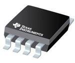
ICGOO电子元器件商城为您提供BQ2057WSNG4由Texas Instruments设计生产,在icgoo商城现货销售,并且可以通过原厂、代理商等渠道进行代购。 BQ2057WSNG4价格参考。Texas InstrumentsBQ2057WSNG4封装/规格:PMIC - 电池充电器, Charger IC Lithium-Ion/Polymer 8-SOIC。您可以下载BQ2057WSNG4参考资料、Datasheet数据手册功能说明书,资料中有BQ2057WSNG4 详细功能的应用电路图电压和使用方法及教程。
BQ2057WSNG4是Texas Instruments(德州仪器)推出的一款PMIC(电源管理集成电路),属于电池充电器类别。该器件主要应用于便携式设备中的锂离子和锂聚合物电池的线性充电管理。以下是其典型应用场景:

1. 便携式电子产品:
   BQ2057WSNG4广泛用于便携式电子设备,如智能手机、平板电脑、数码相机、蓝牙耳机等。这些设备通常需要高效且稳定的电池充电解决方案,而BQ2057WSNG4能够提供精确的充电电流和电压控制,确保电池安全并延长使用寿命。

2. 医疗设备:
   在便携式医疗设备(如血糖仪、便携式心率监测仪等)中,BQ2057WSNG4可以实现低功耗充电管理,同时支持小型化设计,满足医疗设备对可靠性和精度的严格要求。

3. 物联网(IoT)设备:
   对于依赖电池供电的IoT设备(如智能手表、健康追踪器、环境传感器等),BQ2057WSNG4能够以高效率为电池充电,并通过其内置保护功能(如过压、过流和过温保护)确保系统稳定运行。

4. 工业应用:
   在工业领域,例如手持扫描仪、便携式测试设备等,BQ2057WSNG4的紧凑封装和高性能特性使其成为理想选择。它支持单节锂离子/锂聚合物电池充电,适应多种工作环境。

5. 消费类电子产品:
   包括电子阅读器、便携式游戏机和其他小型消费类设备,BQ2057WSNG4以其简单易用的设计和高度集成的功能,降低了系统复杂性并缩短开发周期。

 特点与优势:
- 支持最高2A充电电流,适用于快速充电需求。
- 内置热调节功能,防止过热损坏。
- 提供涓流充电、恒流充电和恒压充电三种模式,优化充电过程。
- 小型WSG4封装,节省PCB空间。
- 集成多种保护机制,提升系统安全性。

综上所述,BQ2057WSNG4适用于需要高效、安全和紧凑型电池充电解决方案的各种便携式设备和应用场合。
| 参数 | 数值 |
| 产品目录 | 集成电路 (IC)半导体 |
| 描述 | IC LITH-ION LDO CHRG MGMT 8-SOIC电池管理 Li-Ion LDO Linear Charge Management IC |
| 产品分类 | |
| 品牌 | Texas Instruments |
| 产品手册 | |
| 产品图片 |
|
| rohs | 符合RoHS无铅 / 符合限制有害物质指令(RoHS)规范要求 |
| 产品系列 | 电源管理 IC,电池管理,Texas Instruments BQ2057WSNG4- |
| 数据手册 | |
| 产品型号 | BQ2057WSNG4 |
| 产品种类 | 电池管理 |
| 产品类型 | Charge Management |
| 供应商器件封装 | 8-SOIC |
| 功能 | 充电管理 |
| 包装 | 管件 |
| 单位重量 | 76 mg |
| 商标 | Texas Instruments |
| 安装类型 | 表面贴装 |
| 安装风格 | SMD/SMT |
| 封装 | Tube |
| 封装/外壳 | 8-SOIC(0.154",3.90mm 宽) |
| 封装/箱体 | SOIC-8 |
| 工作温度 | -20°C ~ 70°C |
| 工作电源电压 | 4.5 V to 15 V |
| 工厂包装数量 | 75 |
| 最大工作温度 | + 70 C |
| 最小工作温度 | - 20 C |
| 标准包装 | 75 |
| 温度监测 | Temperature Monitoring |
| 电压-电源 | 4.5 V ~ 15 V |
| 电池化学 | 锂离子,锂聚合物 |
| 电池类型 | Li-Ion, Li-Polymer |
| 系列 | BQ2057W |
| 输出电压 | 8.4 V |
| 输出电流 | 2 A |
| 配用 | /product-detail/zh/DV2057W/296-9503-ND/379688 |


- 商务部:美国ITC正式对集成电路等产品启动337调查
- 曝三星4nm工艺存在良率问题 高通将骁龙8 Gen1或转产台积电
- 太阳诱电将投资9.5亿元在常州建新厂生产MLCC 预计2023年完工
- 英特尔发布欧洲新工厂建设计划 深化IDM 2.0 战略
- 台积电先进制程称霸业界 有大客户加持明年业绩稳了
- 达到5530亿美元!SIA预计今年全球半导体销售额将创下新高
- 英特尔拟将自动驾驶子公司Mobileye上市 估值或超500亿美元
- 三星加码芯片和SET,合并消费电子和移动部门,撤换高东真等 CEO
- 三星电子宣布重大人事变动 还合并消费电子和移动部门
- 海关总署:前11个月进口集成电路产品价值2.52万亿元 增长14.8%


PDF Datasheet 数据手册内容提取
(cid:1)(cid:2)(cid:3)(cid:4)(cid:5)(cid:6)(cid:7) (cid:1)(cid:2)(cid:3)(cid:4)(cid:5)(cid:6)(cid:8) (cid:1)(cid:2)(cid:3)(cid:4)(cid:5)(cid:6)(cid:9)(cid:7) (cid:1)(cid:2)(cid:3)(cid:4)(cid:5)(cid:6)(cid:10) SLUS025F − MAY 2001 − REVISED JULY 2002 (cid:11)(cid:12)(cid:13)(cid:11)(cid:14)(cid:8)(cid:15)(cid:12) (cid:16)(cid:17)(cid:14)(cid:15)(cid:11)(cid:18) (cid:8)(cid:19)(cid:11)(cid:18)(cid:20)(cid:15) (cid:21)(cid:11)(cid:14)(cid:11)(cid:20)(cid:15)(cid:21)(cid:15)(cid:14)(cid:9) (cid:17)(cid:8) (cid:22)(cid:23)(cid:18) (cid:24)(cid:17)(cid:14)(cid:20)(cid:16)(cid:15)(cid:25) (cid:11)(cid:14)(cid:12) (cid:9)(cid:10)(cid:23)(cid:25)(cid:8)(cid:15)(cid:16)(cid:16) (cid:16)(cid:17)(cid:9)(cid:19)(cid:17)(cid:26)(cid:21)(cid:25)(cid:17)(cid:23)(cid:14) (cid:11)(cid:14)(cid:12) (cid:16)(cid:17)(cid:9)(cid:19)(cid:17)(cid:26)(cid:21)(cid:25)(cid:27)(cid:23)(cid:16)(cid:28)(cid:21)(cid:15)(cid:18) FEATURES DESCRIPTION (cid:1) Ideal for Single (4.1 V or 4.2 V) and Dual-Cell (8.2 V or 8.4 V) Li-Ion or Li-Pol Packs The BENCHMARQ bq2057 series advanced (cid:1) Lithium-Ion (Li-Ion) and Lithium-Polymer (Li-Pol) linear Requires Small Number of External charge-management ICs are designed for cost- Components sensitive and compact portable electronics. They (cid:1) 0.3 V Dropout Voltage for Minimizing Heat combine high-accuracy current and voltage regulation, Dissipation battery conditioning, temperature monitoring, charge (cid:1) Better Than ±1% Voltage Regulation Accuracy termination, charge-status indication, and AutoComp With Preset Voltages charge-rate compensation in a single 8-pin IC. MSOP, (cid:1) AutoComp(cid:2) Dynamic Compensation of TSSOP, and SOIC package options are offered to fit a Battery Pack’s Internal Impedance to Reduce wide range of end applications. Charge Time The bq2057 continuously measures battery (cid:1) Optional Cell-Temperature Monitoring Before temperature using an external thermistor. For safety, and During Charge the bq2057 inhibits charge until the battery temperature (cid:1) Integrated Voltage and Current Regulation is within user-defined thresholds. The bq2057 then With Programmable Charge-Current and High- charges the battery in three phases: conditioning, or Low-Side Current Sensing constant current, and constant voltage. If the battery (cid:1) Integrated Cell Conditioning for Reviving voltage is below the low-voltage threshold, V(min), the bq2057 precharges using a low current to condition the Deeply Discharged Cells and Minimizing Heat battery. The conditioning charge rate is approximately Dissipation During Initial Stage Of Charge 10% of the regulation current. The conditioning current (cid:1) Charge Status Output for Single or Dual Led also minimizes heat dissipation in the external pass- or Host Processor Interface element during the initial stage of the charge. After (cid:1) Automatic Battery-Recharge Feature conditioning, the bq2057 applies a constant current to (cid:1) Charge Termination by Minimum Current the battery. An external sense-resistor sets the current. (cid:1) The sense-resistor can be on either the high or low side Automatic Low-Power Sleep Mode When V CC of the battery without additional components. The Is Removed constant-current phase continues until the battery (cid:1) EVMs Available for Quick Evaluation reaches the charge-regulation voltage. (cid:1) Packaging: 8-Pin SOIC, 8-Pin TSSOP, 8-Pin MSOP bq2057xSN or bq2057xTS bq2057xDGK SOIC (SN) or TSSOP (TS) PACKAGE MSOP (DGK) PACKAGE (TOP VIEW) (TOP VIEW) SNS 1 8 COMP VCC 1 8 BAT BAT 2 7 CC TS 2 7 SNS VCC 3 6 VSS STAT 3 6 COMP TS 4 5 STAT VSS 4 5 CC Please be aware that an important notice concerning availability, standard warranty, and use in critical applications of TexasInstruments semiconductor products and disclaimers thereto appears at the end of this data sheet. AutoComp is a trademark of Texas Instruments. (cid:27)(cid:18)(cid:23)(cid:12)(cid:26)(cid:8)(cid:9)(cid:17)(cid:23)(cid:14) (cid:12)(cid:11)(cid:9)(cid:11) (cid:29)(cid:30)(cid:31)!"#$%(cid:29)!(cid:30) (cid:29)& ’("")(cid:30)% $& !(cid:31) *((cid:1)+(cid:29)’$%(cid:29)!(cid:30) ,$%)- Copyright 2002, Texas Instruments Incorporated (cid:27)"!,(’%& ’!(cid:30)(cid:31)!"# %! &*)’(cid:29)(cid:31)(cid:29)’$%(cid:29)!(cid:30)& *)" %.) %)"#& !(cid:31) (cid:9))/$& (cid:17)(cid:30)&%"(#)(cid:30)%& &%$(cid:30),$", 0$""$(cid:30)%1- (cid:27)"!,(’%(cid:29)!(cid:30) *"!’)&&(cid:29)(cid:30)2 ,!)& (cid:30)!% (cid:30))’)&&$"(cid:29)+1 (cid:29)(cid:30)’+(,) %)&%(cid:29)(cid:30)2 !(cid:31) $++ *$"$#)%)"&- www.ti.com 1
(cid:1)(cid:2)(cid:3)(cid:4)(cid:5)(cid:6)(cid:7) (cid:1)(cid:2)(cid:3)(cid:4)(cid:5)(cid:6)(cid:8) (cid:1)(cid:2)(cid:3)(cid:4)(cid:5)(cid:6)(cid:9)(cid:7) (cid:1)(cid:2)(cid:3)(cid:4)(cid:5)(cid:6)(cid:10) SLUS025F − MAY 2001 − REVISED JULY 2002 DESCRIPTION (continued) The bq2057 then begins the constant-voltage phase. The accuracy of the voltage regulation is better than ±1% over the operating-temperature and supply-voltage ranges. For single and dual cells, the bq2057 is offered in four fixed-voltage versions: 4.1 V, 4.2 V, 8.2 V, and 8.4 V. Charge stops when the current tapers to the charge termination threshold, I . The bq2057 automatically restarts the charge if the battery voltage falls below (TERM) the V threshold. (RCH) The designer also may use the AutoComp feature to reduce charging time. This proprietary technique allows safe and dynamic compensation for the internal impedance of the battery pack during charge. AVAILABLE OPTIONS PACKAGE TA CHARGE REGULATION SOIC TSSOP MSOP† VOLTAGE (SN) (TS) (DGK) 4.1 V Not available bq2057TS bq2057DGK 4.2 V bq2057CSN bq2057CTS bq2057CDGK −−2200°°CC ttoo 7700°°CC 8.2 V Not available bq2057TTS NNoott aavvaaiillaabbllee 8.4 V bq2057WSN bq2057WTS †Note the difference in pinout for this package. 2 www.ti.com
(cid:1)(cid:2)(cid:3)(cid:4)(cid:5)(cid:6)(cid:7) (cid:1)(cid:2)(cid:3)(cid:4)(cid:5)(cid:6)(cid:8) (cid:1)(cid:2)(cid:3)(cid:4)(cid:5)(cid:6)(cid:9)(cid:7) (cid:1)(cid:2)(cid:3)(cid:4)(cid:5)(cid:6)(cid:10) SLUS025F − MAY 2001 − REVISED JULY 2002 function block diagram VCC Internal Reference _ VCC + DONE Sleep Mode _ BAT V-Control + CC I-Control COMP Voltage Regulation G(comp) + _ Battery Recharge VCC + _ VCC Battery Control Conditioning Block STAT _ TS + TS2 Trip _ + TS1 Trip I-Control _ 0.5 VCC High/Low SNS Set + SNS + VCC−V(SNS) _ VSS−V(SNS) Current Regulation + _ Charge Termination VSS www.ti.com 3
(cid:1)(cid:2)(cid:3)(cid:4)(cid:5)(cid:6)(cid:7) (cid:1)(cid:2)(cid:3)(cid:4)(cid:5)(cid:6)(cid:8) (cid:1)(cid:2)(cid:3)(cid:4)(cid:5)(cid:6)(cid:9)(cid:7) (cid:1)(cid:2)(cid:3)(cid:4)(cid:5)(cid:6)(cid:10) SLUS025F − MAY 2001 − REVISED JULY 2002 Terminal Functions TERMINAL NO. II//OO DDEESSCCRRIIPPTTIIOONN NAME SOIC (SN) and MSOP TSSOP (TS) (DGK) BAT 2 8 I Voltage sense input CC 7 5 O Charge control output COMP 8 6 I Charge-rate compensation input (AutoComp) SNS 1 7 I Current sense input STAT 5 3 O Charge status output TS 4 2 I Temperature sense input VCC 3 1 I Supply voltage VSS 6 4 Ground detailed description current-sense input Battery current is sensed via the voltage developed on this pin by an external sense resistor. The external resistor can be placed on either the high or low side of the battery. (See schematics for details.) battery-voltage input Voltage sense-input tied directly to the positive side of the battery. temperature sense input Input for an external battery-temperature monitoring circuit. Connecting this input to VCC/2 disables this feature. charge-status output 3-state indication of charge in progress, charge complete, and temperature fault or sleep mode. charge-control output Source-follower output that drives an external pass-transistor (PNP or P-channel MOSFET) for current and voltage regulation. charge-rate compensation input Sets the charge-rate compensation level. The voltage-regulation output may be programmed to vary as a function of the charge current delivered to the battery. supply voltage input Power supply input and current reference for high-side sensing configuration. 4 www.ti.com
(cid:1)(cid:2)(cid:3)(cid:4)(cid:5)(cid:6)(cid:7) (cid:1)(cid:2)(cid:3)(cid:4)(cid:5)(cid:6)(cid:8) (cid:1)(cid:2)(cid:3)(cid:4)(cid:5)(cid:6)(cid:9)(cid:7) (cid:1)(cid:2)(cid:3)(cid:4)(cid:5)(cid:6)(cid:10) SLUS025F − MAY 2001 − REVISED JULY 2002 absolute maximum ratings over operating free-air temperature (unless otherwise noted)† Supply voltage (V with respect to GND). . . . . . . . . . . . . . . . . . . . . . . . . . . . . . . . . . . . . . . . . . . . . . . . . . −0.3 to +18 V CC Input voltage, SNS, BAT, TS, COMP (all with respect to GND). . . . . . . . . . . . . . . . . . . . . . . . . . −0.3 V to V +0.3 V CC Sink current (STAT pin) not to exceed P . . . . . . . . . . . . . . . . . . . . . . . . . . . . . . . . . . . . . . . . . . . . . . . . . . . . . . . . . 20 mA D Source current (STAT pin) not to exceed P . . . . . . . . . . . . . . . . . . . . . . . . . . . . . . . . . . . . . . . . . . . . . . . . . . . . . . 10 mA D Output current (CC pin) not to exceed P . . . . . . . . . . . . . . . . . . . . . . . . . . . . . . . . . . . . . . . . . . . . . . . . . . . . . . . . 40 mA D Total power dissipation, P (at 25°C) . . . . . . . . . . . . . . . . . . . . . . . . . . . . . . . . . . . . . . . . . . . . . . . . . . . . . . . . . . . 300mW D Operating free-air temperature range, T . . . . . . . . . . . . . . . . . . . . . . . . . . . . . . . . . . . . . . . . . . . . . . . . . . −20°C to 70°C A Storage temperature range, T . . . . . . . . . . . . . . . . . . . . . . . . . . . . . . . . . . . . . . . . . . . . . . . . . . . . . . . . −40°C to 125°C stg Lead temperature (soldering, 10 s) . . . . . . . . . . . . . . . . . . . . . . . . . . . . . . . . . . . . . . . . . . . . . . . . . . . . . . . . . . . . . . 300°C †Stresses beyond those listed under “absolute maximum ratings” may cause permanent damage to the device. These are stress ratings only, and functional operation of the device at these or any other conditions beyond those indicated under “recommended operating conditions” is not implied. Exposure to absolute-maximum-rated conditions for extended periods may affect device reliability. DISSIPATION RATING TABLE DERATING FACTOR TA ≤ 25°C TA = 70°C PACKAGE ABOVE TA = 25°C POWER RATING POWER RATING DGK 3.4 mW/°C 424 mW 271 mW recommended operating conditions MIN MAX UNIT Supply voltage, VCC 4.5 15 V Operating free-air temperature range, TA −20 70 °C electrical characteristics over recommended operating free-air temperature range (unless otherwise noted) PARAMETER TEST CONDITIONS MIN TYP MAX UNIT I(VCC) VCC Current VCC > VCC(min), Excluding external loads 2 4 mA For bq2057 and bq2957C, V(BAT) ≥ V(min), V(BAT) – VCC ≥ 0.8 V 3 6 II((VVCCCCSS)) VVCCCC SSlleeeepp ccuurrrreenntt µAA For bq2057T and bq2957W, V(BAT) ≥ V(min), V(BAT) – VCC ≥ 0.8 V 10 IIB(BAT) Input bias current on BAT pin V(BAT) = V(REG) 1 µA IIB(SNS) Input bias current on SNS pin V(SNS)= 5 V 5 µA IIB(TS) Input bias current on TS pin V(TS) = 5 V 5 µA IIB(COMP) Input bias current on COMP pin V(COMP) = 5 V 5 µA BATTERY VOLTAGE REGULATION bq2057, See Notes 1, 2, 3 4.059 4.10 4.141 bq2057C, See Notes 1, 2, 3 4.158 4.20 4.242 VVOO((RREEGG)) OOuuttppuutt vvoollttaaggee VV bq2057T, See Notes 1, 2, 3 8.119 8.20 8.282 bq2057W, See Notes 1, 2, 3 8.317 8.40 8.484 NOTES: 1. For high-side current sensing configuration 2. For low-side current sensing configuration, the tolerance is ±1% for TA = 25°C and ±1.2% for −20°C ≥ TA ≥70°C 3. V(BAT)+0.3 V ≤VCC ≤VCC(max) www.ti.com 5
(cid:1)(cid:2)(cid:3)(cid:4)(cid:5)(cid:6)(cid:7) (cid:1)(cid:2)(cid:3)(cid:4)(cid:5)(cid:6)(cid:8) (cid:1)(cid:2)(cid:3)(cid:4)(cid:5)(cid:6)(cid:9)(cid:7) (cid:1)(cid:2)(cid:3)(cid:4)(cid:5)(cid:6)(cid:10) SLUS025F − MAY 2001 − REVISED JULY 2002 electrical characteristics over recommended operating free-air temperature range (unless otherwise noted) (continued) PARAMETER TEST CONDITIONS MIN TYP MAX UNIT CURRENT REGULATION bq2057 and bq2057C, 95.4 105 115.5 High-side current sensing configuration bq2057T and bq2057W, 113.6 125 137.5 CCuurrrreenntt rreegguullaattiioonn High-side current sensing configuration VV((SSNNSS)) threshold bq2057 and bq2057C, mmVV 100 110 121 Low-side current sensing configuration bq2057T and bq2057W, 118.1 130 143 Low-side current sensing configuration CHARGE TERMINATION DETECTION Charge termination Voltage at pin SNS, relative to VCC for high-side I(TERM) current detect sensing, and to Vss for low-side sensing, −24 −14 −4 mV threshold 0°C ≤ TA ≤ 50°C TEMPERATURE COMPARATOR Lower temperature V(TS1) threshold 29.1 30 30.9 TTSS ppiinn vvoollttaaggee %%VVCCCC Upper temperature V(TS2) threshold 58.3 60 61.8 PRECHARGE COMPARATOR bq2057 2.94 3 3.06 PPrreecchhaarrggee bq2057C 3.04 3.1 3.16 VV((mmiinn)) tthhrreesshhoolldd bq2057T 5.98 6.1 6.22 VV bq2057W 6.18 6.3 6.43 PRECHARGE CURRENT REGULATION Voltage at pin SNS, relative to VCC for high-side sensing, and to VSS for low-side sensing, 13 mV II((PPRREECCHHGG)) Prreerggeuucllhaaattiiroognne current 0°C ≤ TA ≤ 50°C Voltage at pin SNS, relative to VCC for high-side 3 13 22 mV sensing, 0°C ≤ TA ≤ 50°C, VCC = 5 V VRCH COMPARATOR (Battery Recharge Threshold) VO(REG)− VO(REG)− VO(REG)− bq2057 and bq2057C RReecchhaarrggee 98 mV 100 mV 102 mV VV((RRCCHH)) threshold VO(REG)− VO(REG)− VO(REG)− VV bq2057T and bq2057W 196 mV 200 mV 204 mV CHARGE-RATE COMPENSATION (AutoComp) V(BAT)+0.3 V ≤ VCC ≤ VCC(max), bq2057, bq2057C, 1.87 2.2 2.53 bq2057T, bq2057W GG((CCOOMMPP)) AAuuttooCCoommpp ggaaiinn V(BAT)+0.3 V ≤ VCC ≤ VCC(max), bq2057T and VV//VV 2.09 2.4 2.76 bq2057W in low-side sensing configuration STAT PIN Output (low) VOL(STAT) voltage IOL = 10 mA 0.7 VV Output (high) VOH(STAT) voltage IOH = 5 mA VCC-0.5 CC PIN VOL(CC) Output low voltage IO(CC) = 5 mA (sink) 1.5 V IO(CC) Sink current Not to exceed power rating specification (PD) 5 40 mA 6 www.ti.com
(cid:1)(cid:2)(cid:3)(cid:4)(cid:5)(cid:6)(cid:7) (cid:1)(cid:2)(cid:3)(cid:4)(cid:5)(cid:6)(cid:8) (cid:1)(cid:2)(cid:3)(cid:4)(cid:5)(cid:6)(cid:9)(cid:7) (cid:1)(cid:2)(cid:3)(cid:4)(cid:5)(cid:6)(cid:10) SLUS025F − MAY 2001 − REVISED JULY 2002 APPLICATION INFORMATION RSNS Q1 0.2 Ω FZT788B PACK+ DC+ C1 0.1 µF VCC R1 PACK− 1 kΩ NTC bq2057 VCC CC COMP RT1 SNS BAT TEMP VCC TS C2 0.1 µF VSS STAT Battery D1 Pack GND RT2 R2 2 kΩ Figure 1. Low Dropout Single- or Two-Cell Li-Ion/Li-Pol Charger functional description The bq2057 is an advanced linear charge controller for single or two-cell Li-Ion or Li-Pol applications. Figure 1 shows the schematic of charger using a PNP pass transistor. Figure 2 is an operational state diagram, and Figure 3 is a typical charge profile. Figure 4 shows the schematic of a charger using P-channel MOSFET. www.ti.com 7
(cid:1)(cid:2)(cid:3)(cid:4)(cid:5)(cid:6)(cid:7) (cid:1)(cid:2)(cid:3)(cid:4)(cid:5)(cid:6)(cid:8) (cid:1)(cid:2)(cid:3)(cid:4)(cid:5)(cid:6)(cid:9)(cid:7) (cid:1)(cid:2)(cid:3)(cid:4)(cid:5)(cid:6)(cid:10) SLUS025F − MAY 2001 − REVISED JULY 2002 APPLICATION INFORMATION POR Sleep Mode VCCheCc k>e Vd( aBtA ATl)l No Indicate SLEEP Times MODE (STAT = Hi-Z) Yes Suspend Charge TS Pin Indicate CHARGE in TS1 to TS2 No Range SUSPEND (STAT = Hi-Z) Yes Regulate I(PRECHG) V(BAT) < V(min) Yes Indicate Charge In-Progress (STAT = High) Suspend Charge No TS Pin Indicate CHARGE in TS1 to TS2 No SUSPEND CurreRnetg ourl aVtoeltage Range (STAT = Hi-Z) Indicate Charge In-Progress Yes (STAT = High) TS Pin in TS1 to TS2 Suspend Charge No V(BAT) < V(min) Range TS Pin No in TS1 to TS2 Indicate CHARGE No Range SUSPEND (STAT = Hi-Z) Yes TS Pin Yes in TS1 to TS2 Range Yes No V(BAT) < V(min) Yes No Terminate Charge Yes DI(TetEeRctMed) Yes IndicatDe oCnHeARGE V(BAT) < V(RCH) No (STAT = Low) Yes Figure 2. Operation Flowchart 8 www.ti.com
(cid:1)(cid:2)(cid:3)(cid:4)(cid:5)(cid:6)(cid:7) (cid:1)(cid:2)(cid:3)(cid:4)(cid:5)(cid:6)(cid:8) (cid:1)(cid:2)(cid:3)(cid:4)(cid:5)(cid:6)(cid:9)(cid:7) (cid:1)(cid:2)(cid:3)(cid:4)(cid:5)(cid:6)(cid:10) SLUS025F − MAY 2001 − REVISED JULY 2002 APPLICATION INFORMATION Preconditioning Current Regulation Voltage Regulation and Charge Phase Phase Termination Phase Regulation Voltage Regulation Current Minimum Charge Voltage Preconditioning and Taper Detect Figure 3. Typical Charge Profile qualification and precharge When power is applied, the bq2057 starts a charge-cycle if a battery is already present or when a battery is inserted. Charge qualification is based on battery temperature and voltage. The bq2057 suspends charge if the battery temperature is outside the V(TS1) to V(TS2) range and suspends charge until the battery temperature is within the allowed range. The bq2057 also checks the battery voltage. If the battery voltage is below the precharge threshold V , the bq2057 uses precharge to condition the battery. The conditioning charge rate (min) I is set at approximately 10% of the regulation current. The conditioning current also minimizes heat (PRECHG) dissipation in the external pass-element during the initial stage of charge. See Figure 3 for a typical charge-profile. www.ti.com 9
(cid:1)(cid:2)(cid:3)(cid:4)(cid:5)(cid:6)(cid:7) (cid:1)(cid:2)(cid:3)(cid:4)(cid:5)(cid:6)(cid:8) (cid:1)(cid:2)(cid:3)(cid:4)(cid:5)(cid:6)(cid:9)(cid:7) (cid:1)(cid:2)(cid:3)(cid:4)(cid:5)(cid:6)(cid:10) SLUS025F − MAY 2001 − REVISED JULY 2002 APPLICATION INFORMATION Q1 SI6475DQ RSNS D1 0.2 Ω PACK+ Battery DC+ Pack C2 R2 0.1 µF 1 kΩ PACK− NTC U1 bq2057 RT1 CC COMP SNS BAT TEMP VCC TS VSS STAT R4 RT2 511 Ω U2 C1 0.1 µF R5 1 kΩ CMD67− R3 1 kΩ 22SRUC GND Figure 4. 0.5-A Charger Using P-Channel MOSFET current regulation phase The bq2057 regulates current while the battery-pack voltage is less than the regulation voltage, V . The O(REG) bq2057 monitors charge current at the SNS input by the voltage drop across a sense-resistor, R , in series SNS with the battery pack. In high-side current sensing configuration (Figure 5), R is between the VCC and SNS SNS pins, and in low-side sensing (Figure 6) the R is between VSS (battery negative) and SNS (charger ground) SNS pins. Charge-current feedback, applied through pin SNS, maintains a voltage of V across the current sense (SNS) resistor. The following formula calculates the value of the sense resistor: V (1) (SNS) R (cid:1) SNS I O(REG) Where I is the desired charging current. O(REG) 10 www.ti.com
(cid:1)(cid:2)(cid:3)(cid:4)(cid:5)(cid:6)(cid:7) (cid:1)(cid:2)(cid:3)(cid:4)(cid:5)(cid:6)(cid:8) (cid:1)(cid:2)(cid:3)(cid:4)(cid:5)(cid:6)(cid:9)(cid:7) (cid:1)(cid:2)(cid:3)(cid:4)(cid:5)(cid:6)(cid:10) SLUS025F − MAY 2001 − REVISED JULY 2002 APPLICATION INFORMATION DC+ DC+ RSNS BAT+ BAT+ bq2057 bq2057 SNS COMP SNS COMP BAT CC BAT CC VCC VSS VCC VSS TS STAT TS STAT DC− DC− BAT− RSNS BAT− Figure 5. High-Side Current Sensing Figure 6. Low-Side Current Sensing voltage regulation phase The voltage regulation feedback is through the BAT pin. This input is tied directly to the positive side of the battery pack. The bq2057 monitors the battery-pack voltage between the BAT and VSS pins. The bq2057 is offered in four fixed-voltage versions: 4.1 V, 4.2 V, 8.2 V and 8.4 V. Other regulation voltages can be achieved by adding a voltage divider between the positive and negative terminals of the battery pack and using bq2057T or bq2057W. The voltage divider presents scaled battery-pack voltage to BAT input. (See Figure 7 and Figure 8.) The resistor values RB1 and RB2 for the voltage divider are calculated by the following equation: (cid:2) (cid:4) (2) RB1(cid:1) N(cid:3) V(CELL) –1 R V B2 O(REG) Where: N = Number of cells in series V = Desired regulation voltage per cell (CELL) www.ti.com 11
(cid:1)(cid:2)(cid:3)(cid:4)(cid:5)(cid:6)(cid:7) (cid:1)(cid:2)(cid:3)(cid:4)(cid:5)(cid:6)(cid:8) (cid:1)(cid:2)(cid:3)(cid:4)(cid:5)(cid:6)(cid:9)(cid:7) (cid:1)(cid:2)(cid:3)(cid:4)(cid:5)(cid:6)(cid:10) SLUS025F − MAY 2001 − REVISED JULY 2002 APPLICATION INFORMATION DC+ DC+ RSNS BAT+ BAT+ RB1 RB1 bq2057 bq2057 SNS COMP SNS COMP BAT CC RB2 BAT CC RB2 VCC VSS BAT− VCC VSS BAT− TS STAT TS STAT DC− RSNS DC− Figure 7. Optional Voltage Divider for Figure 8. Optional Voltage Divider for Nonstandard Regulation Voltage, Nonstandard Regulation Voltage, (High-Side Current Sensing) (Low-Side Current Sensing) charge termination and recharge The bq2057 monitors the charging current during the voltage-regulation phase. The bq2057 declares a done condition and terminates charge when the current tapers off to the charge termination threshold, I . A new (TERM) charge cycle begins when the battery voltage falls below the V threshold. (RCH) battery temperature monitoring The bq2057 continuously monitors temperature by measuring the voltage between the TS and VSS pins. A negative- or a positive-temperature coefficient thermistor (NTC, PTC) and an external voltage divider typically develop this voltage. (See Figure 9.) The bq2057 compares this voltage against its internal V and V (TS1) (TS2) thresholds to determine if charging is allowed. (See Figure 10.) The temperature sensing circuit is immune to any fluctuation in V , since both the external voltage divider and the internal thresholds (V and V ) CC (TS1) (TS2) are referenced to VCC. The resistor values of R and R are calculated by the following equations: (T1) (T2) For NTC Thermistors 5(cid:3)R (cid:3)R (3) R (cid:1) (cid:2) TH TC(cid:4) T1 3(cid:3) R (cid:5)R TC TH 5(cid:3)R (cid:3)R (4) RT2(cid:1)(cid:6)(cid:2) T(cid:4)H(cid:2) TC (cid:4)(cid:7) 2(cid:3)R – 7(cid:3)R TC TH 12 www.ti.com
(cid:1)(cid:2)(cid:3)(cid:4)(cid:5)(cid:6)(cid:7) (cid:1)(cid:2)(cid:3)(cid:4)(cid:5)(cid:6)(cid:8) (cid:1)(cid:2)(cid:3)(cid:4)(cid:5)(cid:6)(cid:9)(cid:7) (cid:1)(cid:2)(cid:3)(cid:4)(cid:5)(cid:6)(cid:10) SLUS025F − MAY 2001 − REVISED JULY 2002 APPLICATION INFORMATION battery temperature monitoring (continued) For PTC Thermistors 5(cid:3)R (cid:3)R (5) R (cid:1) (cid:2) TH TC(cid:4) T1 3(cid:3) R (cid:5)R TH TC 5(cid:3)R (cid:3)R (6) RT2(cid:1)(cid:6)(cid:2) T(cid:4)H(cid:2) TC (cid:4)(cid:7) 2(cid:3)R – 7(cid:3)R TH TC Where R is the cold temperature resistance and R is the hot temperature resistance of thermistor, as (TC) (TH) specified by the thermistor manufacturer. RT1 or RT2 can be omitted If only one temperature (hot or cold) setting is required. Applying a voltage between the V(TS1) and V(TS2) thresholds to pin TS disables the temperature-sensing feature. DC+ DC+ RSNS BAT+ BAT+ bq2057 bq2057 RT1 SNS COMP SNS COMP BAT CC BAT CC DC− VCC VSS VCC VSS TS STAT TS STAT RT1 DC− RT2 Thermistor BAT− RT2 Thermistor BAT− RSNS High-Side Current Sensing Low-Side Current Sensing Figure 9. Temperature Sensing Circuits VCC Temperature Fault V(TS2) Normal Temperature Range V(TS1) Temperature Fault VSS Figure 10. bq2057 TS Input Thresholds www.ti.com 13
(cid:1)(cid:2)(cid:3)(cid:4)(cid:5)(cid:6)(cid:7) (cid:1)(cid:2)(cid:3)(cid:4)(cid:5)(cid:6)(cid:8) (cid:1)(cid:2)(cid:3)(cid:4)(cid:5)(cid:6)(cid:9)(cid:7) (cid:1)(cid:2)(cid:3)(cid:4)(cid:5)(cid:6)(cid:10) SLUS025F − MAY 2001 − REVISED JULY 2002 APPLICATION INFORMATION charge inhibit function The TS pin can be used as charge-inhibit input. The user can inhibit charge by connecting the TS pin to VCC or VSS (or any level outside the V(TS1) to V(TS2) thresholds). Applying a voltage between the V(TS1) and V(TS2) thresholds to pin TS returns the charger to normal operation. charge status indication The bq2057 reports the status of the charger on the 3-state STAT pin. The following table summarized the operation of the STAT pin. CONDITION STAT PIN Battery conditioning and charging High Charge complete (Done) Low Temperature fault or sleep mode Hi-Z The STAT pin can be used to drive a single LED (Figure 1), dual-chip LEDs (Figure 4) or for interface to a host or system processor (Figure 11). When interfacing the bq2057 to a processor, the user can use an output port, as shown in Figure 11, to recognize the high-Z state of the STAT pin. In this configuration, the user needs to read the input pin, toggle the output port and read the STAT pin again. In a high-Z condition, the input port always matches the signal level on the output port. Host bq2057CTS Processor SNS COMP BAT CC OUT VCC VSS TS STAT IN Figure 11. Interfacing the bq2057 to a Host Processor low-power sleep mode The bq2057 enters the sleep mode if the VCC falls below the voltage at the BAT input. This feature prevents draining the battery pack during the absence of VCC. 14 www.ti.com
(cid:1)(cid:2)(cid:3)(cid:4)(cid:5)(cid:6)(cid:7) (cid:1)(cid:2)(cid:3)(cid:4)(cid:5)(cid:6)(cid:8) (cid:1)(cid:2)(cid:3)(cid:4)(cid:5)(cid:6)(cid:9)(cid:7) (cid:1)(cid:2)(cid:3)(cid:4)(cid:5)(cid:6)(cid:10) SLUS025F − MAY 2001 − REVISED JULY 2002 APPLICATION INFORMATION selecting an external pass-transistor The bq2057 is designed to work with both PNP transistor and P-channel MOSFET. The device should be chosen to handle the required power dissipation, given the circuit parameters, PCB layout and heat sink configuration. The following examples illustrate the design process for either device: PNP transistor: Selection steps for a PNP bipolar transistor: Example: VI = 4.5 V, I(REG) = 1 A, 4.2-V single-cell Li-Ion (bq2057C). V is the input voltage to the charger and I is the desired charge current (see Figure 1). I (REG) 1. Determine the maximum power dissipation, P , in the transistor. D The worst case power dissipation happens when the cell voltage, V , is at its lowest (typically 3 V at the (BAT) beginning of current regulation phase) and V is at its maximum. I Where V is the voltage drop across the current sense resistor. CS P = (V − V – V ) × IREG (7) D I CS (BAT) P = (4.5 – 0.1 − 3) × 1 A D P = 1.4 W D 2. Determine the package size needed in order to keep the junction temperature below the manufacturer’s recommended value, T . Calculate the total theta, θ(°C/W), needed. (J)max (cid:2) (cid:4) (8) T (cid:5)T (J)max A(max) θ (cid:1) JC P D (150–40) θ (cid:1) JC 1.4 θ (cid:1)78°C(cid:8)W JC Now choose a device package with a theta at least 10% below this value to account for additional thetas other than the device. A SOT223 package, for instance, has typically a theta of 60°C/W. 3. Select a collector-emitter voltage, V , rating greater than the maximum input voltage. A 15-V device will (CE) be adequate in this example. 4. Select a device that has at least 50% higher drain current I rating than the desired charge current I . C (REG) 5. Using the following equation, calculate the minimum beta (β or h ) needed: FE I (9) (cid:1) (cid:1) CMAX min I B (cid:1) (cid:1) 1 min 0.035 (cid:1) (cid:1)28 min where I is the maximum collector current (in this case same as I ), and I is the base current max(C)) (REG) B (chosen to be 35 mA in this example). NOTE: The beta of a transistor drops off by a factor of 3 over temperature and also drops off with load. Therefore, note the beta of device at I and the minimum ambient temperature when choosing (REG) the device. This beta should be larger than the minimum required beta. Now choose a PNP transistor that is rated for V(CE) ≥15 V, θJC ≤ 78°C/W, IC ≥ 1.5 A, βmin ≥ 28 and that is in a SOT223 package. www.ti.com 15
(cid:1)(cid:2)(cid:3)(cid:4)(cid:5)(cid:6)(cid:7) (cid:1)(cid:2)(cid:3)(cid:4)(cid:5)(cid:6)(cid:8) (cid:1)(cid:2)(cid:3)(cid:4)(cid:5)(cid:6)(cid:9)(cid:7) (cid:1)(cid:2)(cid:3)(cid:4)(cid:5)(cid:6)(cid:10) SLUS025F − MAY 2001 − REVISED JULY 2002 APPLICATION INFORMATION selecting an external pass-transistor (continued) P-channel MOSFET: Selection steps for a P-channel MOSFET: Example: VI = 5.5 V, I(REG) = 500 mA, 4.2-V single-cell Li−Ion (bq2057C). V is the input voltage to the charger and I is the desired charge current. (See Figure 4.) I (REG) 1. Determine the maximum power dissipation, P , in the transistor. D The worst case power dissipation happens when the cell voltage, V , is at its lowest (typically 3 V at (BAT) the beginning of current regulation phase) and V is at its maximum. I Where V is the forward voltage drop across the reverse-blocking diode (if one is used), and V is the D CS voltage drop across the current sense resistor. P = (V – V − V – V ) × I (10) D I D (CS) (BAT) (REG) P = (5.5 – 0.4 – 0.1 −3) × 0.5 A D PD = 1 W 2. Determine the package size needed in order to keep the junction temperature below the manufacturer’s recommended value, T . Calculate the total theta, θ(°C/W), needed. JMAX (cid:2) (cid:4) (11) T –T max(J) A(max) θ (cid:1) JC P D (150–40) θ (cid:1) JC 1 θ (cid:1)110°C(cid:8)W JC Now choose a device package with a theta at least 10% below this value to account for additional thetas other than the device. A TSSOP-8 package, for instance, has typically a theta of 70°C/W. 3. Select a drain-source voltage, V , rating greater than the maximum input voltage. A 12 V device will be (DS) adequate in this example. 4. Select a device that has at least 50% higher drain current (I ) rating than the desired charge current I . D (REG) 5. Verify that the available drive is large enough to supply the desired charge current. V(GS) = (VD +V(CS) + VOL(CC)) − VI (12) V = (0.4 + 0.1 + 1.5) – 5.5 (GS) V = −3.5 (GS) Where V is the gate-to-source voltage, V is the forward voltage drop across the reverse-blocking diode (GS) D (if one is used), and V is the voltage drop across the current sense resistor, and V is the CC pin CS OL(CC) output low voltage specification for the bq2057. Select a MOSFET with gate threshold voltage, V , rating less than the calculated V . (GSth) (GS) Now choose a P-channel MOSFET transistor that is rated for VDS ≤ −15 V, θJC ≤ 110°C/W, ID ≥ 1 A, V ≥ −3.5 V and in a TSSOP package. (GSth) 16 www.ti.com
(cid:1)(cid:2)(cid:3)(cid:4)(cid:5)(cid:6)(cid:7) (cid:1)(cid:2)(cid:3)(cid:4)(cid:5)(cid:6)(cid:8) (cid:1)(cid:2)(cid:3)(cid:4)(cid:5)(cid:6)(cid:9)(cid:7) (cid:1)(cid:2)(cid:3)(cid:4)(cid:5)(cid:6)(cid:10) SLUS025F − MAY 2001 − REVISED JULY 2002 APPLICATION INFORMATION selecting input capacitor In most applications, all that is needed is a high-frequency decoupling capacitor. A 0.1 µF ceramic, placed in proximity to VCC and VSS pins, works well. The bq2057 works with both regulated and unregulated external dc supplies. If a non-regulated supply is chosen, the supply unit should have enough capacitance to hold up the supply voltage to the minimum required input voltage at maximum load. If not, more capacitance must be added to the input of the charger. selecting output capacitor The bq2057 does not require any output capacitor for loop stability. The user can add output capacitance in order to control the output voltage when a battery is not present. The charger quickly charges the output capacitor to the regulation voltage, but the output voltage decays slowly, because of the low leakage current on the BAT pin, down to the recharge threshold. Addition of a 0.1µF ceramic capacitor, for instance, results in a 100 mV(pp) ripple waveform, with an approximate frequency of 25Hz. Higher capacitor values can be used if a lower frequency is desired. automatic charge-rate compensation To reduce charging time, the bq2057 uses the proprietary AutoComp technique to compensate safely for internal impedance of the battery pack. The AutoComp feature is disabled by connecting the COMP pin to VCC in high-side current-sensing configuration, and to VSS in low-side current-sensing configuration. The COMP pin must not be left floating. Figure 12 outlines the major components of a single-cell Li-Ion battery pack. The Li-Ion battery pack consists of a cell, protection circuit, fuse, connector, current sense-resistors, and some wiring. Each of these components contains some resistance. Total impedance of the battery pack is the sum of the minimum resistances of all battery-pack components. Using the minimum resistance values reduces the odds for overcompensating. Overcompensating may activate the safety circuit of the battery pack. BAT+ Wire Terminal Fuse Cell Protection Controller BAT− Wire Wire Wire Terminal Discharge Charge Figure 12. Typical Components of a Single-Cell Li-Ion Pack Compensation is achieved through input pin COMP (Figure 13). A portion of the current-sense voltage, presented through this pin, is scaled by a factor of G and summed with the regulation threshold, V . (COMP) O(REG) This process increases the output voltage to compensate for the battery pack’s internal impedance and for undesired voltage drops in the circuit. www.ti.com 17
(cid:1)(cid:2)(cid:3)(cid:4)(cid:5)(cid:6)(cid:7) (cid:1)(cid:2)(cid:3)(cid:4)(cid:5)(cid:6)(cid:8) (cid:1)(cid:2)(cid:3)(cid:4)(cid:5)(cid:6)(cid:9)(cid:7) (cid:1)(cid:2)(cid:3)(cid:4)(cid:5)(cid:6)(cid:10) SLUS025F − MAY 2001 − REVISED JULY 2002 APPLICATION INFORMATION automatic charge-rate compensation (continued) AutoComp setup requires the following information: (cid:1) Total impedance of battery pack (Z ) (PACK) (cid:1) Maximum charging current (I ) (REG) The voltage drop across the internal impedance of battery pack, V , can then be calculated using the following (Z) equation: V(Z) = Z(PACK) × I(REG) (13) The required compensation is then calculated using the following equations: V (14) (Z) V (cid:1) (COMP) G (COMP) (cid:2) (cid:4) V (cid:1)V (cid:9) G (cid:3)V (PACK) O(REG) (COMP) (COMP Where V is the voltage on COMP pin. This voltage is referenced to VCC in high-side current sensing (COMP) configuration and to VSS for low-side sensing. V(PACK) is the voltage across the battery pack. The values of R(COMP1) and R(COMP2) can be calculated using the following equation: V R (15) (COMP)(cid:1) COMP2 V R (cid:9)R (SNS) COMP1 COMP2 DC+ DC+ BAT+ RCOMP2 BAT+ RCOMP1 bq2057 RSNS bq2057 SNS COMP SNS COMP BAT CC BAT CC VCC VSS DC− VCC VSS TS STAT TS STAT DC− RCOMP2 RSNS RCOMP1 BAT− High-Side Current Sensing Low-Side Current Sensing Figure 13. AutoComp Circuits 18 www.ti.com
(cid:1)(cid:2)(cid:3)(cid:4)(cid:5)(cid:6)(cid:7) (cid:1)(cid:2)(cid:3)(cid:4)(cid:5)(cid:6)(cid:8) (cid:1)(cid:2)(cid:3)(cid:4)(cid:5)(cid:6)(cid:9)(cid:7) (cid:1)(cid:2)(cid:3)(cid:4)(cid:5)(cid:6)(cid:10) SLUS025F − MAY 2001 − REVISED JULY 2002 APPLICATION INFORMATION automatic charge-rate compensation (continued) The following example illustrates these calculations: Assume Z = 100 mΩ, I = 500 mA, high-side current sensing bq2057C (PACK) (REG) V (cid:1)Z (cid:3)I (16) (Z) (PACK) (REG) V (cid:1)0.1(cid:3)0.5 (Z) V = 50 mV (Z) V (17) (Z) V (cid:1) (COMP) G (COMP) V (cid:1)0.05 (COMP) 2.2 V = 22.7 mV (COMP) Let R = 10 kΩ COMP2 (cid:2) (cid:4) (18) R (cid:3) V (cid:5)V COMP2 (SNS) (COMP) R (cid:1) COMP1 V (COMP) (105mV(cid:5)22.7mV) R (cid:1)10k(cid:3) COMP1 22.7mV R (cid:1)36.25k(cid:2) COMP1 Use the closest standard value (36.0 kΩ) for R COMP1 www.ti.com 19
(cid:1)(cid:2)(cid:3)(cid:4)(cid:5)(cid:6)(cid:7) (cid:1)(cid:2)(cid:3)(cid:4)(cid:5)(cid:6)(cid:8) (cid:1)(cid:2)(cid:3)(cid:4)(cid:5)(cid:6)(cid:9)(cid:7) (cid:1)(cid:2)(cid:3)(cid:4)(cid:5)(cid:6)(cid:10) SLUS025F − MAY 2001 − REVISED JULY 2002 MECHANICAL DATA 8−Pin SOIC Narrow (SN) 8−Pin SN (0.150” SOIC ) Inches Millimeters Dimension Min. Max. Min. Max. (cid:1) (cid:3)(cid:4)(cid:3)(cid:9)(cid:3) (cid:3)(cid:4)(cid:3)(cid:12)(cid:3) (cid:7)(cid:4)(cid:10)(cid:8) (cid:7)(cid:4)(cid:12)(cid:13) (cid:1)(cid:7) (cid:3)(cid:4)(cid:3)(cid:3)(cid:5) (cid:3)(cid:4)(cid:3)(cid:7)(cid:3) (cid:3)(cid:4)(cid:7)(cid:3) (cid:3)(cid:4)(cid:8)(cid:10) (cid:11) (cid:3)(cid:4)(cid:3)(cid:7)(cid:6) (cid:3)(cid:4)(cid:3)(cid:8)(cid:3) (cid:3)(cid:4)(cid:6)(cid:6) (cid:3)(cid:4)(cid:10)(cid:7) (cid:14) (cid:3)(cid:4)(cid:3)(cid:3)(cid:12) (cid:3)(cid:4)(cid:3)(cid:7)(cid:3) (cid:3)(cid:4)(cid:7)(cid:13) (cid:3)(cid:4)(cid:8)(cid:10) (cid:16) (cid:3)(cid:4)(cid:7)(cid:13)(cid:10) (cid:3)(cid:4)(cid:8)(cid:3)(cid:3) (cid:5)(cid:4)(cid:12)(cid:3) (cid:10)(cid:4)(cid:3)(cid:13) (cid:17) (cid:3)(cid:4)(cid:7)(cid:10)(cid:3) (cid:3)(cid:4)(cid:7)(cid:9)(cid:3) (cid:6)(cid:4)(cid:13)(cid:7) (cid:5)(cid:4)(cid:3)(cid:9) (cid:18) (cid:3)(cid:4)(cid:3)(cid:5)(cid:10) (cid:3)(cid:4)(cid:3)(cid:10)(cid:10) (cid:7)(cid:4)(cid:7)(cid:5) (cid:7)(cid:4)(cid:5)(cid:3) (cid:20) (cid:3)(cid:4)(cid:8)(cid:8)(cid:10) (cid:3)(cid:4)(cid:8)(cid:5)(cid:10) (cid:10)(cid:4)(cid:12)(cid:8) (cid:9)(cid:4)(cid:8)(cid:8) (cid:21) (cid:3)(cid:4)(cid:3)(cid:7)(cid:10) (cid:3)(cid:4)(cid:3)(cid:6)(cid:10) (cid:3)(cid:4)(cid:6)(cid:13) (cid:3)(cid:4)(cid:13)(cid:15) TS: 8−Pin TSSOP Inches Millimeters Dimension Min. Max. Min. Max. (cid:1) (cid:3)(cid:4)(cid:3)(cid:5)(cid:6) (cid:7)(cid:4)(cid:7)(cid:3) (cid:2) (cid:2) (cid:1)(cid:7) (cid:3)(cid:4)(cid:3)(cid:3)(cid:8) (cid:3)(cid:4)(cid:3)(cid:3)(cid:9) (cid:3)(cid:4)(cid:3)(cid:10) (cid:3)(cid:4)(cid:7)(cid:10) (cid:11) (cid:3)(cid:4)(cid:3)(cid:3)(cid:12) (cid:3)(cid:4)(cid:3)(cid:7)(cid:8) (cid:3)(cid:4)(cid:7)(cid:13) (cid:3)(cid:4)(cid:6)(cid:3) (cid:14) (cid:3)(cid:4)(cid:3)(cid:3)(cid:5) (cid:3)(cid:4)(cid:3)(cid:3)(cid:12) (cid:3)(cid:4)(cid:3)(cid:15) (cid:3)(cid:4)(cid:7)(cid:13) (cid:16) (cid:3)(cid:4)(cid:7)(cid:7)(cid:5) (cid:3)(cid:4)(cid:7)(cid:8)(cid:8) (cid:8)(cid:4)(cid:15)(cid:3) (cid:6)(cid:4)(cid:7)(cid:3) (cid:17) (cid:3)(cid:4)(cid:7)(cid:9)(cid:15) (cid:3)(cid:4)(cid:7)(cid:12)(cid:9) (cid:5)(cid:4)(cid:6)(cid:3) (cid:5)(cid:4)(cid:5)(cid:13) (cid:18) (cid:3)(cid:4)(cid:3)(cid:8)(cid:10)(cid:9)(cid:11)(cid:19)(cid:14) (cid:3)(cid:4)(cid:9)(cid:10)(cid:11)(cid:19)(cid:14) (cid:20) (cid:3)(cid:4)(cid:8)(cid:5)(cid:9) (cid:3)(cid:4)(cid:8)(cid:10)(cid:9) (cid:9)(cid:4)(cid:8)(cid:10) (cid:9)(cid:4)(cid:10)(cid:3) Notes: 1.Controlling dimension: millimeters. Inches shown for reference only. 2 ’D’ and ’E’ do not include mold flash or protrusions. Mold flash or protrusions shall not exceed 0,15 mm per side 3 Each lead centerline shall be located within±0,10 mm of its exact true position. 4 Leads shall be coplanar within 0,08 mm at the seating plane. 5 Dimension ’B’ does not include dambar protrusion. The dambar protrusion(s) shall not cause the lead width to exceed ’B’ maximum by more than 0,08 mm. 6 Dimension applies to the flat section of the lead between 0,10 mm and 0,25 mm from the lead tip. 7 ’A1’ is defined as the distance from the seating plane to the lowest point of the package body (base plane). www.ti.com 20
PACKAGE OPTION ADDENDUM www.ti.com 6-Feb-2020 PACKAGING INFORMATION Orderable Device Status Package Type Package Pins Package Eco Plan Lead/Ball Finish MSL Peak Temp Op Temp (°C) Device Marking Samples (1) Drawing Qty (2) (6) (3) (4/5) BQ2057CDGK ACTIVE VSSOP DGK 8 80 Green (RoHS NIPDAUAG Level-2-260C-1 YEAR -20 to 70 2057C & no Sb/Br) BQ2057CDGKR ACTIVE VSSOP DGK 8 2500 Green (RoHS NIPDAUAG Level-2-260C-1 YEAR -20 to 70 2057C & no Sb/Br) BQ2057CDGKRG4 ACTIVE VSSOP DGK 8 2500 Green (RoHS NIPDAUAG Level-2-260C-1 YEAR -20 to 70 2057C & no Sb/Br) BQ2057CSN ACTIVE SOIC D 8 75 Green (RoHS NIPDAU Level-1-260C-UNLIM -20 to 70 2057C & no Sb/Br) BQ2057CSNTR ACTIVE SOIC D 8 2500 Green (RoHS NIPDAU Level-1-260C-UNLIM -20 to 70 2057C & no Sb/Br) BQ2057CTS ACTIVE TSSOP PW 8 150 Green (RoHS NIPDAU Level-2-260C-1 YEAR -20 to 70 2057C & no Sb/Br) BQ2057CTSTR ACTIVE TSSOP PW 8 2000 Green (RoHS NIPDAU Level-2-260C-1 YEAR -20 to 70 2057C & no Sb/Br) BQ2057CTSTRG4 ACTIVE TSSOP PW 8 2000 Green (RoHS NIPDAU Level-2-260C-1 YEAR -20 to 70 2057C & no Sb/Br) BQ2057DGK ACTIVE VSSOP DGK 8 80 Green (RoHS NIPDAUAG Level-2-260C-1 YEAR -20 to 70 2057 & no Sb/Br) BQ2057SN ACTIVE SOIC D 8 75 Green (RoHS NIPDAU Level-1-260C-UNLIM -20 to 70 2057 & no Sb/Br) BQ2057SNG4 ACTIVE SOIC D 8 75 Green (RoHS NIPDAU Level-1-260C-UNLIM -20 to 70 2057 & no Sb/Br) BQ2057TS ACTIVE TSSOP PW 8 150 Green (RoHS NIPDAU Level-1-260C-UNLIM -20 to 70 2057 & no Sb/Br) BQ2057TSN ACTIVE SOIC D 8 75 Green (RoHS NIPDAU Level-1-260C-UNLIM -20 to 70 2057T & no Sb/Br) BQ2057TTS ACTIVE TSSOP PW 8 150 Green (RoHS NIPDAU Level-2-260C-1 YEAR -20 to 70 2057T & no Sb/Br) BQ2057TTSG4 ACTIVE TSSOP PW 8 150 Green (RoHS NIPDAU Level-2-260C-1 YEAR -20 to 70 2057T & no Sb/Br) BQ2057TTSTR ACTIVE TSSOP PW 8 2000 Green (RoHS NIPDAU Level-2-260C-1 YEAR -20 to 70 2057T & no Sb/Br) BQ2057TTSTRG4 ACTIVE TSSOP PW 8 2000 Green (RoHS NIPDAU Level-2-260C-1 YEAR -20 to 70 2057T & no Sb/Br) Addendum-Page 1
PACKAGE OPTION ADDENDUM www.ti.com 6-Feb-2020 Orderable Device Status Package Type Package Pins Package Eco Plan Lead/Ball Finish MSL Peak Temp Op Temp (°C) Device Marking Samples (1) Drawing Qty (2) (6) (3) (4/5) BQ2057WSN ACTIVE SOIC D 8 75 Green (RoHS NIPDAU Level-1-260C-UNLIM -20 to 70 2057W & no Sb/Br) BQ2057WSNTR ACTIVE SOIC D 8 2500 Green (RoHS NIPDAU Level-1-260C-UNLIM -20 to 70 2057W & no Sb/Br) BQ2057WSNTRG4 ACTIVE SOIC D 8 2500 Green (RoHS NIPDAU Level-1-260C-UNLIM -20 to 70 2057W & no Sb/Br) BQ2057WTS ACTIVE TSSOP PW 8 150 Green (RoHS NIPDAU Level-2-260C-1 YEAR -20 to 70 2057W & no Sb/Br) BQ2057WTSG4 ACTIVE TSSOP PW 8 150 Green (RoHS NIPDAU Level-2-260C-1 YEAR -20 to 70 2057W & no Sb/Br) BQ2057WTSTR ACTIVE TSSOP PW 8 2000 Green (RoHS NIPDAU Level-2-260C-1 YEAR -20 to 70 2057W & no Sb/Br) (1) The marketing status values are defined as follows: ACTIVE: Product device recommended for new designs. LIFEBUY: TI has announced that the device will be discontinued, and a lifetime-buy period is in effect. NRND: Not recommended for new designs. Device is in production to support existing customers, but TI does not recommend using this part in a new design. PREVIEW: Device has been announced but is not in production. Samples may or may not be available. OBSOLETE: TI has discontinued the production of the device. (2) RoHS: TI defines "RoHS" to mean semiconductor products that are compliant with the current EU RoHS requirements for all 10 RoHS substances, including the requirement that RoHS substance do not exceed 0.1% by weight in homogeneous materials. Where designed to be soldered at high temperatures, "RoHS" products are suitable for use in specified lead-free processes. TI may reference these types of products as "Pb-Free". RoHS Exempt: TI defines "RoHS Exempt" to mean products that contain lead but are compliant with EU RoHS pursuant to a specific EU RoHS exemption. Green: TI defines "Green" to mean the content of Chlorine (Cl) and Bromine (Br) based flame retardants meet JS709B low halogen requirements of <=1000ppm threshold. Antimony trioxide based flame retardants must also meet the <=1000ppm threshold requirement. (3) MSL, Peak Temp. - The Moisture Sensitivity Level rating according to the JEDEC industry standard classifications, and peak solder temperature. (4) There may be additional marking, which relates to the logo, the lot trace code information, or the environmental category on the device. (5) Multiple Device Markings will be inside parentheses. Only one Device Marking contained in parentheses and separated by a "~" will appear on a device. If a line is indented then it is a continuation of the previous line and the two combined represent the entire Device Marking for that device. (6) Lead/Ball Finish - Orderable Devices may have multiple material finish options. Finish options are separated by a vertical ruled line. Lead/Ball Finish values may wrap to two lines if the finish value exceeds the maximum column width. Addendum-Page 2
PACKAGE OPTION ADDENDUM www.ti.com 6-Feb-2020 Important Information and Disclaimer:The information provided on this page represents TI's knowledge and belief as of the date that it is provided. TI bases its knowledge and belief on information provided by third parties, and makes no representation or warranty as to the accuracy of such information. Efforts are underway to better integrate information from third parties. TI has taken and continues to take reasonable steps to provide representative and accurate information but may not have conducted destructive testing or chemical analysis on incoming materials and chemicals. TI and TI suppliers consider certain information to be proprietary, and thus CAS numbers and other limited information may not be available for release. In no event shall TI's liability arising out of such information exceed the total purchase price of the TI part(s) at issue in this document sold by TI to Customer on an annual basis. Addendum-Page 3
PACKAGE MATERIALS INFORMATION www.ti.com 11-Jun-2013 TAPE AND REEL INFORMATION *Alldimensionsarenominal Device Package Package Pins SPQ Reel Reel A0 B0 K0 P1 W Pin1 Type Drawing Diameter Width (mm) (mm) (mm) (mm) (mm) Quadrant (mm) W1(mm) BQ2057CDGKR VSSOP DGK 8 2500 330.0 12.4 5.3 3.4 1.4 8.0 12.0 Q1 BQ2057CSNTR SOIC D 8 2500 330.0 12.4 6.4 5.2 2.1 8.0 12.0 Q1 BQ2057CTSTR TSSOP PW 8 2000 330.0 12.4 7.0 3.6 1.6 8.0 12.0 Q1 BQ2057TTSTR TSSOP PW 8 2000 330.0 12.4 7.0 3.6 1.6 8.0 12.0 Q1 BQ2057WSNTR SOIC D 8 2500 330.0 12.4 6.4 5.2 2.1 8.0 12.0 Q1 BQ2057WTSTR TSSOP PW 8 2000 330.0 12.4 7.0 3.6 1.6 8.0 12.0 Q1 PackMaterials-Page1
PACKAGE MATERIALS INFORMATION www.ti.com 11-Jun-2013 *Alldimensionsarenominal Device PackageType PackageDrawing Pins SPQ Length(mm) Width(mm) Height(mm) BQ2057CDGKR VSSOP DGK 8 2500 367.0 367.0 35.0 BQ2057CSNTR SOIC D 8 2500 367.0 367.0 35.0 BQ2057CTSTR TSSOP PW 8 2000 367.0 367.0 35.0 BQ2057TTSTR TSSOP PW 8 2000 367.0 367.0 35.0 BQ2057WSNTR SOIC D 8 2500 367.0 367.0 35.0 BQ2057WTSTR TSSOP PW 8 2000 367.0 367.0 35.0 PackMaterials-Page2
PACKAGE OUTLINE D0008A SOIC - 1.75 mm max height SCALE 2.800 SMALL OUTLINE INTEGRATED CIRCUIT C SEATING PLANE .228-.244 TYP [5.80-6.19] .004 [0.1] C A PIN 1 ID AREA 6X .050 [1.27] 8 1 2X .189-.197 [4.81-5.00] .150 NOTE 3 [3.81] 4X (0 -15 ) 4 5 8X .012-.020 B .150-.157 [0.31-0.51] .069 MAX [3.81-3.98] .010 [0.25] C A B [1.75] NOTE 4 .005-.010 TYP [0.13-0.25] 4X (0 -15 ) SEE DETAIL A .010 [0.25] .004-.010 0 - 8 [0.11-0.25] .016-.050 [0.41-1.27] DETAIL A (.041) TYPICAL [1.04] 4214825/C 02/2019 NOTES: 1. Linear dimensions are in inches [millimeters]. Dimensions in parenthesis are for reference only. Controlling dimensions are in inches. Dimensioning and tolerancing per ASME Y14.5M. 2. This drawing is subject to change without notice. 3. This dimension does not include mold flash, protrusions, or gate burrs. Mold flash, protrusions, or gate burrs shall not exceed .006 [0.15] per side. 4. This dimension does not include interlead flash. 5. Reference JEDEC registration MS-012, variation AA. www.ti.com
EXAMPLE BOARD LAYOUT D0008A SOIC - 1.75 mm max height SMALL OUTLINE INTEGRATED CIRCUIT 8X (.061 ) [1.55] SYMM SEE DETAILS 1 8 8X (.024) [0.6] SYMM (R.002 ) TYP [0.05] 5 4 6X (.050 ) [1.27] (.213) [5.4] LAND PATTERN EXAMPLE EXPOSED METAL SHOWN SCALE:8X SOLDER MASK SOLDER MASK METAL OPENING OPENING METAL UNDER SOLDER MASK EXPOSED METAL EXPOSED METAL .0028 MAX .0028 MIN [0.07] [0.07] ALL AROUND ALL AROUND NON SOLDER MASK SOLDER MASK DEFINED DEFINED SOLDER MASK DETAILS 4214825/C 02/2019 NOTES: (continued) 6. Publication IPC-7351 may have alternate designs. 7. Solder mask tolerances between and around signal pads can vary based on board fabrication site. www.ti.com
EXAMPLE STENCIL DESIGN D0008A SOIC - 1.75 mm max height SMALL OUTLINE INTEGRATED CIRCUIT 8X (.061 ) [1.55] SYMM 1 8 8X (.024) [0.6] SYMM (R.002 ) TYP [0.05] 5 4 6X (.050 ) [1.27] (.213) [5.4] SOLDER PASTE EXAMPLE BASED ON .005 INCH [0.125 MM] THICK STENCIL SCALE:8X 4214825/C 02/2019 NOTES: (continued) 8. Laser cutting apertures with trapezoidal walls and rounded corners may offer better paste release. IPC-7525 may have alternate design recommendations. 9. Board assembly site may have different recommendations for stencil design. www.ti.com
None
None
PACKAGE OUTLINE PW0008A TSSOP - 1.2 mm max height SCALE 2.800 SMALL OUTLINE PACKAGE C 6.6 TYP SEATING PLANE 6.2 PIN 1 ID A 0.1 C AREA 6X 0.65 8 1 3.1 2X 2.9 NOTE 3 1.95 4 5 0.30 8X 0.19 4.5 1.2 MAX B 0.1 C A B 4.3 NOTE 4 (0.15) TYP SEE DETAIL A 0.25 GAGE PLANE 0.15 0.75 0 - 8 0.05 0.50 DETAIL A TYPICAL 4221848/A 02/2015 NOTES: 1. All linear dimensions are in millimeters. Any dimensions in parenthesis are for reference only. Dimensioning and tolerancing per ASME Y14.5M. 2. This drawing is subject to change without notice. 3. This dimension does not include mold flash, protrusions, or gate burrs. Mold flash, protrusions, or gate burrs shall not exceed 0.15 mm per side. 4. This dimension does not include interlead flash. Interlead flash shall not exceed 0.25 mm per side. 5. Reference JEDEC registration MO-153, variation AA. www.ti.com
EXAMPLE BOARD LAYOUT PW0008A TSSOP - 1.2 mm max height SMALL OUTLINE PACKAGE 8X (1.5) 8X (0.45) SYMM (R0.05) 1 TYP 8 SYMM 6X (0.65) 5 4 (5.8) LAND PATTERN EXAMPLE SCALE:10X SOOPLEDNEINRG MASK METAL MSOELTDAEL RU NMDAESRK SOOPLEDNEINRG MASK 0.05 MAX 0.05 MIN ALL AROUND ALL AROUND NON SOLDER MASK SOLDER MASK DEFINED DEFINED SOLDER MASK DETAILS NOT TO SCALE 4221848/A 02/2015 NOTES: (continued) 6. Publication IPC-7351 may have alternate designs. 7. Solder mask tolerances between and around signal pads can vary based on board fabrication site. www.ti.com
EXAMPLE STENCIL DESIGN PW0008A TSSOP - 1.2 mm max height SMALL OUTLINE PACKAGE 8X (1.5) SYMM (R0.05) TYP 8X (0.45) 1 8 SYMM 6X (0.65) 5 4 (5.8) SOLDER PASTE EXAMPLE BASED ON 0.125 mm THICK STENCIL SCALE:10X 4221848/A 02/2015 NOTES: (continued) 8. Laser cutting apertures with trapezoidal walls and rounded corners may offer better paste release. IPC-7525 may have alternate design recommendations. 9. Board assembly site may have different recommendations for stencil design. www.ti.com
IMPORTANTNOTICEANDDISCLAIMER TI PROVIDES TECHNICAL AND RELIABILITY DATA (INCLUDING DATASHEETS), DESIGN RESOURCES (INCLUDING REFERENCE DESIGNS), APPLICATION OR OTHER DESIGN ADVICE, WEB TOOLS, SAFETY INFORMATION, AND OTHER RESOURCES “AS IS” AND WITH ALL FAULTS, AND DISCLAIMS ALL WARRANTIES, EXPRESS AND IMPLIED, INCLUDING WITHOUT LIMITATION ANY IMPLIED WARRANTIES OF MERCHANTABILITY, FITNESS FOR A PARTICULAR PURPOSE OR NON-INFRINGEMENT OF THIRD PARTY INTELLECTUAL PROPERTY RIGHTS. These resources are intended for skilled developers designing with TI products. You are solely responsible for (1) selecting the appropriate TI products for your application, (2) designing, validating and testing your application, and (3) ensuring your application meets applicable standards, and any other safety, security, or other requirements. These resources are subject to change without notice. TI grants you permission to use these resources only for development of an application that uses the TI products described in the resource. Other reproduction and display of these resources is prohibited. No license is granted to any other TI intellectual property right or to any third party intellectual property right. TI disclaims responsibility for, and you will fully indemnify TI and its representatives against, any claims, damages, costs, losses, and liabilities arising out of your use of these resources. TI’s products are provided subject to TI’s Terms of Sale (www.ti.com/legal/termsofsale.html) or other applicable terms available either on ti.com or provided in conjunction with such TI products. TI’s provision of these resources does not expand or otherwise alter TI’s applicable warranties or warranty disclaimers for TI products. Mailing Address: Texas Instruments, Post Office Box 655303, Dallas, Texas 75265 Copyright © 2020, Texas Instruments Incorporated