 Datasheet下载
- 型号: BP5221A
- 制造商: ROHM Semiconductor
- 库位|库存: xxxx|xxxx
- 要求:
| 数量阶梯 | 香港交货 | 国内含税 |
| +xxxx | $xxxx | ¥xxxx |
查看当月历史价格
查看今年历史价格
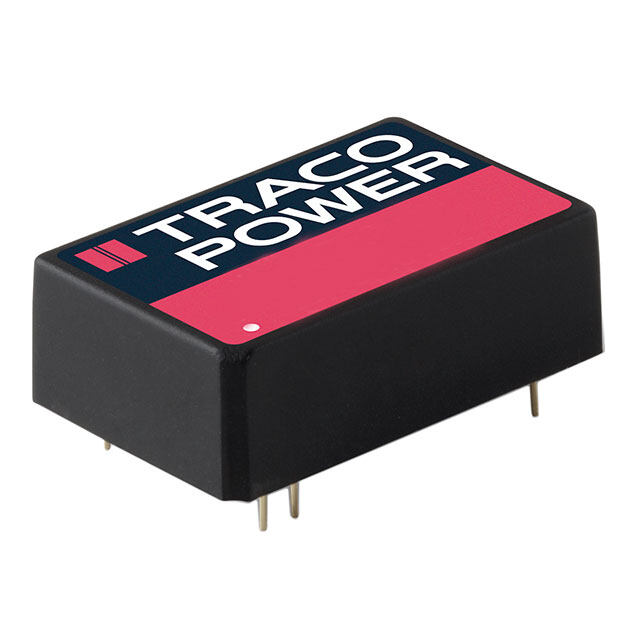
BP5221A产品简介:
ICGOO电子元器件商城为您提供BP5221A由ROHM Semiconductor设计生产,在icgoo商城现货销售,并且可以通过原厂、代理商等渠道进行代购。 BP5221A价格参考。ROHM SemiconductorBP5221A封装/规格:直流转换器, 非隔离 PoL 模块 DC/DC 转换器 1 输出 5V 500mA 8V - 38V 输入。您可以下载BP5221A参考资料、Datasheet数据手册功能说明书,资料中有BP5221A 详细功能的应用电路图电压和使用方法及教程。
BP5221A 是罗姆半导体(Rohm Semiconductor)推出的一款高效同步整流降压型直流转换器(DC-DC Converter)。该芯片主要应用于需要低功耗、高效率和小型化设计的场景,以下为其典型应用场景:

 1. 便携式电子设备
   - 移动电源:BP5221A 的高效性能使其非常适合用于移动电源等便携式充电设备,能够延长电池续航时间。
   - 可穿戴设备:如智能手表、健身追踪器等,这些设备对电源管理要求极高,BP5221A 的小尺寸和低静态电流特性非常匹配。
   - 蓝牙耳机:支持小型化设计,同时提供稳定的电压输出以驱动音频电路。

 2. 物联网(IoT)设备
   - 传感器模块:在智能家居、工业自动化等领域,BP5221A 可为各种低功耗传感器提供稳定电源。
   - 无线通信模块:如 Wi-Fi、Zigbee 或 LoRa 模块,BP5221A 能够高效地将电池电压转换为模块所需的稳定工作电压。

 3. 消费类电子产品
   - 数码相机/摄像机:为图像处理单元和存储设备提供稳定的电源供应。
   - 手持游戏机:满足其对高效电源管理和长时间运行的需求。

 4. 汽车电子
   - 车载信息娱乐系统:BP5221A 的宽输入电压范围和高可靠性使其适合用作车内电子设备的电源解决方案。
   - 远程钥匙进入系统(RKE):为低功耗射频收发器供电,确保系统的长期稳定运行。

 5. 医疗电子
   - 便携式健康监测设备:如血糖仪、血氧仪等,BP5221A 的高精度输出电压和低噪声特性有助于提高测量准确性。
   - 助听器:支持微型化设计,同时保证足够的输出功率。

 6. 其他应用
   - 无线充电器:为接收端的二次调节提供高效的电源管理方案。
   - 低功耗 MCU 供电:为微控制器及其外围电路提供稳定的电源支持。

BP5221A 的主要优势在于其高效率、低静态电流(Iq)、紧凑封装以及出色的热性能,这使得它在各种低功耗、空间受限的应用中表现出色。
| 参数 | 数值 |
| 产品目录 | |
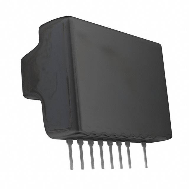
| 描述 | CONVERTER DC/DC 5V OUT .5A 9-SIP稳压器—开关式稳压器 HIC REGULATOR DC-DC 5V 500mA |
| 产品分类 | DC DC Converters集成电路 - IC |
| 品牌 | Rohm Semiconductor |
| 产品手册 | |
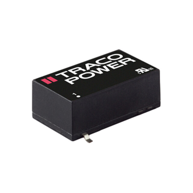
| 产品图片 |
|
| rohs | 符合RoHS无铅 / 符合限制有害物质指令(RoHS)规范要求 |
| 产品系列 | 电源管理 IC,稳压器—开关式稳压器,ROHM Semiconductor BP5221ABP5221 |
| 数据手册 | |
| 产品型号 | BP5221A |
| 产品目录页面 | |
| 产品种类 | 稳压器—开关式稳压器 |
| 功率(W)-制造系列 | 2W |
| 功率(W)-最大值 | 2.5W |
| 包装 | 散装 |
| 商标 | ROHM Semiconductor |
| 大小/尺寸 | 1.10" 长 x 0.47" 宽 x 0.77" 高(28.0mm x 12.0mm x 19.5mm) |
| 安装类型 | 通孔 |
| 安装风格 | Through Hole |
| 封装 | Bulk |
| 封装/外壳 | 9-SIP 模块(8 引线) |
| 封装/箱体 | SIP-9 Module |
| 工作温度 | -20°C ~ 70°C |
| 工厂包装数量 | 150 |
| 开关频率 | 190 kHz |
| 效率 | 84% |
| 最大输入电压 | 38 V |
| 标准包装 | 150 |
| 特性 | - |
| 电压-输入(最大值) | 38V |
| 电压-输入(最小值) | 8V |
| 电压-输出1 | 5V |
| 电压-输出2 | - |
| 电压-输出3 | - |
| 电压-隔离 | - |
| 电流-输出(最大值) | 500mA |
| 类型 | 非隔离 PoL 模块 |
| 输出数 | 1 |
| 输出电压 | 5 V |
| 输出电流 | 500 mA |
| 输出端数量 | 1 Output |


- 商务部:美国ITC正式对集成电路等产品启动337调查
- 曝三星4nm工艺存在良率问题 高通将骁龙8 Gen1或转产台积电
- 太阳诱电将投资9.5亿元在常州建新厂生产MLCC 预计2023年完工
- 英特尔发布欧洲新工厂建设计划 深化IDM 2.0 战略
- 台积电先进制程称霸业界 有大客户加持明年业绩稳了
- 达到5530亿美元!SIA预计今年全球半导体销售额将创下新高
- 英特尔拟将自动驾驶子公司Mobileye上市 估值或超500亿美元
- 三星加码芯片和SET,合并消费电子和移动部门,撤换高东真等 CEO
- 三星电子宣布重大人事变动 还合并消费电子和移动部门
- 海关总署:前11个月进口集成电路产品价值2.52万亿元 增长14.8%


PDF Datasheet 数据手册内容提取
Data Sheet Step-down DC/DC Converters(Non-isolated) BP5220A / BP5221A / BP5222A Description Dimensions (Unit : mm) The BP5220A, BP5221A, BP5222A, are DC / DC converters that use a pulse width modulation (PWM) 28.0 Max. 12.0 system. They contain control circuits, switching devices, Max. rectifiers, and coils, and operate by only connecting an Marked side Ic9 o/- pnOivn es SrmsIPiooo npt,ha tichnkega mgcaeopsd awucliietthos r n.a Wore hi taehva aat ilshaiinbgklhe r eienfqf isuctiiaerennddc.-ya olof npeo wer 19.5 Max. Marked side They can be applied to various purposes by fine-tuning Pin No.1 2 3 4 5 6 7 9 4±1 the output voltage and switching on and off. With a wide 2.54 0.5 range of input voltage, the modules are best suited for 1.4 4.0 8.0 obtaining a stable local power supply from a main 2.54x8=20.32 Max. Max. power supply with a large voltage variation. Note : Dimensions without tolerance is typical. Applications SIP9 Power supplies for copiers, personal computers, facsimiles, AV equipment, measuring instruments, vending machines, security device, registers, industrial equipment, and maintenance tools Features 1) Wide input voltage range 2) High power conversion efficiency. 3) Built-in output ON / OFF switch. 4) Adjustable output voltage ensures wide compatibility 5) Few external components required. 6) Heat sink unnecessary. 7) Compact package. BP5220A / BP5221A / BP5222A : SIP9 Lineup BP5220A BP5221A BP5222A Unit Input voltage 8 to 38 8 to 38 15 to 38 V Output voltage 5 5 12 V Output current 1 0.5 0.5 A Power conversion 85 84 90 efficiency (Vi=15V) (Vi=15V) (Vi=20V) % Absolute maximum ratings (Ta=25°C) Limits Parameter Symbol Unit BP5220A BP5221A BP5222A Input voltage Vi 8 to 38 8 to 38 15 to 38 V Output current IO 1 0.5 0.5 A Operating temperature range Topr °C Storage temperature range Tstg °C www.rohm.com 1/7 2011.10 - Rev. C © 2011 ROHM Co., Ltd. All rights reserved.
BP5220A/BP5221A/BP5222A Data Sheet Block diagram BP5220A / BP5221A / BP5222A DRIVE CIRCUIT POWER SUPPLY CONTROL CIRCUIT CIRCUIT N. C. N. C. 9 7 6 5 4 3 2 1 Vi ADJ N. C. CTL GND VOUT FB Electrical characteristics BP5220A (Unless otherwise noted : Vi=15V, Io=0.5A, SW=1, Ta=25˚C) Parameter Symbol Min. Typ. Max. Unit Conditions Input voltage Vi 8 38 V Output voltage VO 4.75 5 5.25 V Output current IO 1 A Vi<30V Line regulation 27 80 mV Vi=8V to 38V Load regulation 13 80 mV Io=0.1A to 1A Output ripple voltage 22 70 mVPP Power conversion efficiency 75 85 % Io=1A Switching frequency fSW 190 kHz CTL pin ON resistance RON 4.7 Vo>4.75V CTL pin OFF resistance ROFF 200 Vo<0.1V, SW=2 BP5221A (Unless otherwise noted : Vi=15V, Io=0.25A, SW=1, Ta=25˚C) Parameter Symbol Min. Typ. Max. Unit Conditions Input voltage Vi 8 38 V Output voltage VO 4.75 5 5.25 V Output current IO 0.5 A Line regulation 13 50 mV Vi=8V to 38V Load regulation 3 50 mV Io=0.05A to 0.5A Output ripple voltage 25 70 mVPP Power conversion efficiency 70 84 % Io=1A Switching frequency fSW 190 kHz CTL pin ON resistance RON 4.7 Vo>4.75V CTL pin OFF resistance ROFF 200 Vo<0.1V, SW=2 www.rohm.com 2/7 2011.10 - Rev. C © 2011 ROHM Co., Ltd. All rights reserved.
BP5220A/BP5221A/BP5222A Data Sheet BP5222A (Unless otherwise noted : Vi=20V, Io=0.25A, SW=1, Ta=25˚C) Parameter Symbol Min. Typ. Max. Unit Conditions Input voltage Vi 15 38 V Output voltage VO 11.2 12 12.8 V Output current IO 0.5 A Line regulation 22 50 mV Vi=15V to 38V Load regulation 18 50 mV Io=0.05A to 0.5A Output ripple voltage 29 70 mVPP Power conversion efficiency 75 90 % Io=0.5A Switching frequency fSW 190 kHz CTL pin ON resistance RON 4.7 Vo>11.2V CTL pin OFF resistance ROFF 200 Vo<0.1V, SW=2 Measurement circuit BP5220A / BP5221A / BP5222A 9 7 6 5 4 3 2 1 Input Output A A SW 1 2 + + V V f 4.7k 200k f ; Frequency counter Fig.1 T Switching frequency=1/T Output ripple voltage Please note that output ripple voltage depends on the type and characteristics of the output capacitor. www.rohm.com 3/7 2011.10 - Rev. C © 2011 ROHM Co., Ltd. All rights reserved.
BP5220A/BP5221A/BP5222A Data Sheet Circuit operation (1) The basic application examples are shown in Fig.2. BP5220A / BP5221A / BP5222A The only external parts required are the input and output smoothing capacitors. 9 7 6 5 4 3 2 1 Vi VO (2) Switching on and off the output voltage is allowed. Be sure to use fuse for safety. The output can be switched off by making pin 4 + + open (high impedance). (See Fig.3) (3) Fine adjustment of the output voltage is allowed. Fig.2 Adjustment of the output voltage can be performed from pin 6 via the resistor by connecting the output terminal (pin 2) or GND. (See BP5220A / BP5221A / BP5222A application example 3) Output OFF Be sure to use fuse for safety. 9 7 6 5 4 3 2 1 Vi VO SW + + Fig.3 Application Examples Application Example 1 : DC / DC converter with protection circuit BP5220A / BP5221A / BP5222A 6 Vi 9 7 6 5 4 3 2 1 VO 5 24V 5V + + E (V) 4 AG Vi =24V LT 3 O V T 120pF PU 2 + T U COMP. O 1 BA10393 0 0.2 0.4 0.6 0.8 1.0 1.2 OUTPUT CURRENT (A) Fig.4 Fig.5 A resistor is used to limit the rise of output at power on. The resistance depends on the input voltage. This is a standard application. Because the control current fluctuates with variations in circuits and components, set the control current by adding a sufficient margin to the normal current level. Application Example 2 : Output ON / OFF control BP5220A / BP5221A / BP5222A Be sure to use fuse for safety. 9 7 6 5 4 3 2 1 Vi VO + + 100 F 470 F ON / OFF 100k 2SC1740 k 0 0 1 Fig.6 www.rohm.com 4/7 2011.10 - Rev. C © 2011 ROHM Co., Ltd. All rights reserved.
BP5220A/BP5221A/BP5222A Data Sheet Application Example 3 : Output voltage adjustment (1) When reducing the output voltage (2) When increasing the output voltage BP5220A / BP5221A / BP5222A BP5220A / BP5221A / BP5222A 9 7 6 5 4 3 2 1 9 7 6 5 4 3 2 1 Vi VO Vi VO + Be sure to use + + Be sure to use VR + fuse for safety. 100 F fuse for safety. 470 F VR Fig.8 Fig.7 VR value setting equations (The output voltage after adjustment is denoted by Vo.) (1) When reducing the output voltage BP5220A / BP5221A BP5222A (2) When increasing the output voltage BP5220A / BP5221A BP5222A To maximize performance we recommended the output voltage be adjusted within ±20% of the output voltage rating. When the output voltage is increased by 20%, for instance, the minimum input voltage is also increased by 20%. (Example : When the output voltage is changed from 5V to 6V in the BP5220A, the minimum input voltage is charged from 8V to 9.6V) Application Example 4 : Slow start The slow start circuit mitigates the pulse load on the internal switching transistor when input voltage is applied, and increases the output voltage gradually by starting the switching operation slowly. This application is useful for preventing malfunction of an external protection circuit due to rush current, and can serve as a countermeasure against operation outside the safe operation range. BP5220A / BP5221A / BP5222A 9 7 6 5 4 3 2 1 Vi VO 24V + + Be sure to use 470 F 100 F fuse for safety. 470k 2SC1740R k + C1 00 10 F 1 Fig.9 C1 is a slow-start capacitor for mitigating excessive rush current that flows into the module when the switch is turned on. www.rohm.com 5/7 2011.10 - Rev. C © 2011 ROHM Co., Ltd. All rights reserved.
BP5220A/BP5221A/BP5222A Data Sheet Operation notes (1) No circuit is installed in the modules to protect against excessive output currents. Therefore, take physical safety measures such as using a fuse if short-circuit loading is probable. (2) The output current should be reduced according to an increase in the input voltage or ambient temperature. Use the modules within the derating curve range. (3) A large rush current may flow in the module when the input voltage is applied or the output ON / OFF is controlled with pin 4 without a capacitor such as C1 in application 4. Operating within the safe operation ranges shown in Fig.12, 15, and 18. The safe operation range is determined by the safe operation range of the internal switching transistor. The amount of rush current depends on the output impedance of the input power supply and capacitors connected to the module outputs. The pulse load on the internal switching transistor at the start of operation can be reduced by using the protection circuit in application 1 or the slow start circuit in application 4. (4) Pins 5 and 7 are not connected. (5) A smoothing electrolytic capacitor is necessary for I/O external components. Please use a capacitor equivalent to the recommended one. (6) Please put an I/O smoothing capacitor near the module. Output ripple voltage may be larger or output voltage may not be stable. Electrical Characteristics Curves BP5220A 1200 100 20 Vi=8V Pw=0.2ms OUTPUT CURRENT : I (mA)O1086420000000000 VVii==3348VV VVViii===823 50toVV 15V 86420000 VVii==2338VV UTPUT CURRENT INTO PIN9 (A) 0001...05321532 TScIN=G25L°EC PULSE Pw=1ms O 0.1 0 25 50 70 100 120 0 200 400 600 800 1000 1 2 3 5 10 2030 50 AMBIENT TEMPERATURE : Ta(°C) OUTPUT CURRENT : IO (mA) VOLTAGE BETWEEN PIN2 AND PIN9 (V) Fig.10 Derating curve Fig.11 Efficiency Fig.12 Safety operation range BP5221A 10 0.6 100 Vi=8V A) Pw=1ms mA) 0.5 Vi=8 to 15V 80 Vi=23V PIN9 (4.5A OUTPUT CURRENT : I (O 0000....4321 Vi=30 to 38V 642000 Vi=38V OUTPUT CURRENT INTO 2.2A1 TScIN=G2P5Lw°E=C 1P0UmLSsE 0.1 1 10 100 0 25 50 70 100 120 0 0.1 0.2 0.3 0.4 0.5 AMBIENT TEMPERATURE : Ta(°C) OUTPUT CURRENT : IO (A) VOLTAGE BETWEEN PIN2 AND PIN9 (V) Fig.13 Derating curve Fig.14 Efficiency Fig.15 Safety operation range www.rohm.com 6/7 2011.10 - Rev. C © 2011 ROHM Co., Ltd. All rights reserved.
BP5220A/BP5221A/BP5222A Data Sheet BP5222A 0.6 100 10 Vi=23V mA) 0.5 Vi=15 to 20V 80 Vi=38V N9 (A)4.5A Pw=1ms RENT : I (O 00..43 VVii==3308VV 60 Vi=30V NT INTO PI2.2A1 Pw=10ms R E U R C 40 R UT 0.2 CU TP UT Tc=25°C OU 0.1 20 TP SINGLE PULSE U O 0.1 0 25 50 70 100 120 0 0.1 0.2 0.3 0.4 0.5 1 10 100 AMBIENT TEMPERATURE : Ta(°C) OUTPUT CURRENT : IO (A) VOLTAGE BETWEEN PIN2 AND PIN9 (V) Fig.16 Derating curve Fig.17 Efficiency Fig.18 Safety operation range Pin 9 sink current BP5220A / BP5221A / BP5222A 9 7 6 5 4 3 2 1 + + Voltage difference between pins 2 and 9 Fig.19 ASO measurement circuit www.rohm.com 7/7 2011.10 - Rev. C © 2011 ROHM Co., Ltd. All rights reserved.
None