ICGOO在线商城 > BD6586MUV-E2
 Datasheet下载
- 型号: BD6586MUV-E2
- 制造商: ROHM Semiconductor
- 库位|库存: xxxx|xxxx
- 要求:
| 数量阶梯 | 香港交货 | 国内含税 |
| +xxxx | $xxxx | ¥xxxx |
查看当月历史价格
查看今年历史价格
BD6586MUV-E2产品简介:
ICGOO电子元器件商城为您提供BD6586MUV-E2由ROHM Semiconductor设计生产,在icgoo商城现货销售,并且可以通过原厂、代理商等渠道进行代购。 提供BD6586MUV-E2价格参考¥29.15-¥29.15以及ROHM SemiconductorBD6586MUV-E2封装/规格参数等产品信息。 你可以下载BD6586MUV-E2参考资料、Datasheet数据手册功能说明书, 资料中有BD6586MUV-E2详细功能的应用电路图电压和使用方法及教程。
| 参数 | 数值 |
| 产品目录 | 集成电路 (IC)光电子产品 |
| 描述 | IC LED DRVR WHITE BCKLGT 24-VQFNLED照明驱动器 24 LEDs 2.7-5.5V 24V Max Out 25mA Out |
| 产品分类 | |
| 品牌 | Rohm Semiconductor |
| 产品手册 | |
| 产品图片 |
|
| rohs | 符合RoHS无铅 / 符合限制有害物质指令(RoHS)规范要求 |
| 产品系列 | LED照明电子器件,LED照明驱动器,ROHM Semiconductor BD6586MUV-E2- |
| 数据手册 | |
| 产品型号 | BD6586MUV-E2 |
| 产品目录页面 | |
| 产品种类 | LED照明驱动器 |
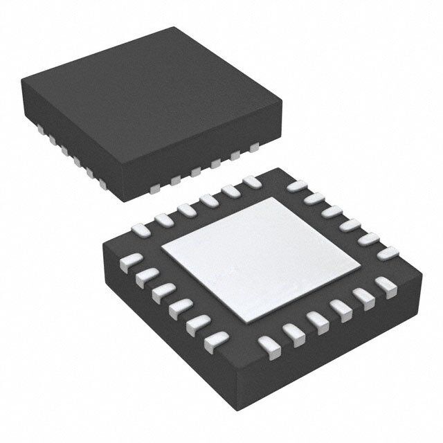
| 供应商器件封装 | VQFN024V4040 |
| 其它名称 | BD6586MUV-E2TR |
| 内部驱动器 | 是 |
| 功率耗散 | 1510 mW |
| 包装 | 带卷 (TR) |
| 商标 | ROHM Semiconductor |
| 安装类型 | 表面贴装 |
| 安装风格 | SMD/SMT |
| 封装 | Reel |
| 封装/外壳 | 24-VFQFN 裸露焊盘 |
| 封装/箱体 | VQFN-24 |
| 工作温度 | -40°C ~ 85°C |
| 工厂包装数量 | 2500 |
| 恒压 | - |
| 恒流 | - |
| 拓扑 | PWM,升压(升压) |
| 最大工作温度 | + 85 C |
| 最大电源电流 | 25 mA |
| 最小工作温度 | - 40 C |
| 标准包装 | 2,500 |
| 电压-电源 | 2.7 V ~ 5.5 V |
| 电压-输出 | 24V |
| 类型-初级 | 背光 |
| 类型-次级 | 白色 LED |
| 输入电压 | 2.7 V to 5.5 V |
| 输出数 | 4 |
| 频率 | 700kHz ~ 1.3MHz |


- 商务部:美国ITC正式对集成电路等产品启动337调查
- 曝三星4nm工艺存在良率问题 高通将骁龙8 Gen1或转产台积电
- 太阳诱电将投资9.5亿元在常州建新厂生产MLCC 预计2023年完工
- 英特尔发布欧洲新工厂建设计划 深化IDM 2.0 战略
- 台积电先进制程称霸业界 有大客户加持明年业绩稳了
- 达到5530亿美元!SIA预计今年全球半导体销售额将创下新高
- 英特尔拟将自动驾驶子公司Mobileye上市 估值或超500亿美元
- 三星加码芯片和SET,合并消费电子和移动部门,撤换高东真等 CEO
- 三星电子宣布重大人事变动 还合并消费电子和移动部门
- 海关总署:前11个月进口集成电路产品价值2.52万亿元 增长14.8%


PDF Datasheet 数据手册内容提取
Datasheet 4-Channel White LED Driver with Integrated FET for up to 24 LEDs BD6586MUV ●General Description ●Key Specifications BD6586MUV is white LED driver IC with PWM step-up Operating power supply voltage range: 2.7V to 5.5V DC/DC converter that can boost max 24V and current LED maximum current: 25mA (Max.) driver that can drive max 25mA. The wide and Quiescent Current: 0.1μA (Typ.) precision brightness can be controlled by external Switching frequency: 1.0MHz(Typ.) PWM pulse. Operating temperature range: -40℃ to +85℃ BD6586MUV has very accurate current drivers, and it has few current errors between each strings. So, it will ●Package W(Typ.) x D(Typ.) x H(Max.) be helpful to reduce brightness spots on the LCD. Small package type is suited for saving space. ●Features ■ High accuracy & good matching (±3.0%) current drivers 4ch (MAX.25mA/ch) ■ 28V power Nch MOSFET ■ Soft Start ■ Drive up to 6 in series, 4 strings in parallel ■ Rich safety functions ▪ Over-voltage protection VQFN024V4040 ▪ Output Short protection 4.00mm x 4.00mm x 1.00mm ▪ External SBD open detect ▪ Over current limit ▪ Thermal shutdown Figure 1. ▪ UVLO ●Applications All middle size LCD equipments backlight of Notebook PC, portable DVD player, car navigation systems, etc. ●Typical Application Circuit Battery 2.7V to 5.5V 4.7μF 4.7μH 6LED x 4Parallel 2.2μF 1μF SW SW SW VBAT VDET TRSW EN2 100Hz~1kHz PWM LED1 EN1 LED2 PWM LED3 TESTO LED4 TEST PGND PGND GND GND GND ISET Each 20mA Can be set up to each 10~25mA 24kΩ Figure 2. Typical Application Circuit (Power control PWM application) ○Product structure:Silicon monolithic integrated circuit ○This product is not designed protection against radioactive rays www.rohm.com TSZ02201-0G3G0C400190-1-2 © 2012 ROHM Co., Ltd. All rights reserved. 1/20 TSZ22111・14・001 10.Dec.2012 Rev.001
Datasheet BD6586MUV ●Absolute Maximum Ratings (Ta=25 ℃) Parameter Symbol Ratings Unit Condition VBAT, EN1, EN2, TRSW, Terminal voltage 1 VMAX1 7 V PWM,TESTO, ISET, TEST Terminal voltage 2 VMAX2 25 V LED1, LED2, LED3, LED4, Terminal voltage 3 VMAX3 30.5 V SW Terminal voltage 4 VMAX4 50.5 V VDET Power dissipation 1 Pd1 500 *1 mW Power dissipation 2 Pd2 780 *2 mW Power dissipation 3 Pd3 1510 *3 mW Operating temperature range Topr -40 to +85 ℃ Storage temperature range Tstg -55 to +150 ℃ *1 Reduced 4.0mW/ ℃ With Ta>25 ℃ when not mounted on a heat radiation Board. *2 1 layer (ROHM Standard board) has been mounted. Copper foil area 0mm2, When it’s used by more than Ta=25 ℃, it’s reduced by 6.2mW/ ℃. *3 4 layer (JEDEC Compliant board) has been mounted. Copper foil area 1layer 6.28mm2, Copper foil area 2 to 4layers 5655.04mm2, When it’s used by more than Ta=25 ℃, it’s reduced by 12.1mW/ ℃. ●Recommended Operating Rating (Ta=-40 ℃ to +85 ℃) Limits Parameter Symbol Unit Condition Min. Typ. Max. Power supply voltage VBAT 2.7 3.6 5.5 V ●Electrical Characteristics (Unless otherwise specified, VBAT=3.6V, Ta = +25 ℃) Limits Parameter Symbol Unit Condition Min. Typ. Max. [EN1, EN2, PWM Terminal] EN threshold voltage (Low) VthL 0 - 0.4 V EN threshold voltage (High) VthH 1.4 - 5.5 V EN terminal input current Iin - 8.3 16.0 µA Input=2.5V [Under Voltage Lock Out] Under Voltage Lock Out UVLO 2.05 2.35 2.65 V VBAT falling edge [Switching Regulator] Quiescent Current Iq - 0.1 2.0 µA EN1=EN2=PWM=0V Current Consumption Idd - 2.2 4.6 mA VDET=0V,ISET=24kΩ LED Control voltage VLED 0.4 0.5 0.6 V Over Current Limit Ocp 1.1 1.5 2.5 A *1 SBD Open Protect Sop - - 0.1 V Detect voltage of VDET pin Switching frequency fSW 0.7 1.0 1.3 MHz Duty cycle limit Duty 91 95 99 % LED1-4=0.3V Over voltage limit Ovl 25.0 25.5 26.0 V LED1-4=0.3V SW Transistor On Resistance RSW - 0.24 0.32 Ω Isw=100mA [Current driver] LED maximum current ILMAX - - 25 mA LED current accuracy ILACCU - - ±5 % ILED=20mA ▪Each LED current/Average (LED1-4) LED current matching ILMAT - - ±3 % ▪ILED=20mA ISET voltage Iset 0.5 0.6 0.7 V Current limit value at ISET LED current limiter ILOCP 35 60 90 mA resistance 4.7kΩ setting LED1, 2, 3, 4=0.5V LED Terminal LEDOVP 10.0 11.5 13.0 V EN1=EN2=PWM=2.5V Over Voltage Protect *1 This parameter is tested with DC measurement. www.rohm.com TSZ02201-0G3G0C400190-1-2 © 2012 ROHM Co., Ltd. All rights reserved. 2/20 TSZ22111・15・001 10.Dec.2012 Rev.001
Datasheet BD6586MUV ●Pin Descriptions Terminal equivalent PIN Name In/Out PIN number Function circuit diagram 1 VBAT In Battery input G 2 EN1 In Power control pin A 3 EN2 In Power control pin A 4 GND - GND for DC/DC B 5 PWM In PWM input pin for power ON/OFF only driver A 6 ISET In Register connection for LED current setting D 7 GND - GND for ISET Register B 8 LED1 In Current sink for LED1 C 9 LED2 In Current sink for LED2 C 10 GND - GND for Current Driver B 11 LED3 In Current sink for LED3 C 12 LED4 In Current sink for LED4 C 13 TEST In TEST input (Pull down 100kΩ to GND) A 14 TESTO Out TEST output D 15 N.C. - No connect pin E 16 SW Out Switching Tr drive Pin F 17 SW Out Switching Tr drive Pin F 18 SW Out Switching Tr drive Pin F 19 VDET In Detect input for SBD open and OVP C 20 N.C. - No connect pin E 21 PGND - PGND for switching transistor D 22 PGND - PGND for switching transistor D 23 N.C. - No connect pin E 24 TRSW Out The gate of Switching Tr D Thermal Heat radiation PAD of back side - - - PAD Connect to GND ●Pin ESD Type VBAT VBAT PIN PIN PIN GND PGND GND A B C VBAT PIN PIN PIN GND PGND D E F PIN GND PGND G Figure 3. Pin ESD Type www.rohm.com TSZ02201-0G3G0C400190-1-2 © 2012 ROHM Co., Ltd. All rights reserved. 3/20 TSZ22111・15・001 10.Dec.2012 Rev.001
Datasheet BD6586MUV ●Block Diagram Current SENSE Pin number 24pin Figure 4. Block diagram ●Description of Functions 1) PWM current mode DC/DC converter While BD6586MUV is power ON, the lowest voltage of LED1, 2, 3, 4 is detected, PWM duty is decided to be 0.5V and output voltage is kept invariably. As for the inputs of the PWM comparator as the feature of the PWM current mode, one is overlapped with error components from the error amplifier, and the other is overlapped with a current sense signal that controls the inductor current into Slope waveform to prevent sub harmonic oscillation. This output controls internal Nch Tr via the RS latch. In the period where internal Nch Tr gate is ON, energy is accumulated in the external inductor, and in the period where internal Nch Tr gate is OFF, energy is transferred to the output capacitor via external SBD. BD6586MUV has many safety functions, and their detection signals stop switching operation at once. 2) Soft start BD6586MUV has soft start function. The soft start function prevents large coil current. Rush current at turning on is prevented by the soft start function. After EN1, EN2 are changed L H, soft start becomes effective for within 1ms and soft start doesn't become effective even if EN1, EN2 are changed L H after that. And, when the H section of PWM is within 1ms, soft start becomes invalid when PWM is input to H more than three times. The invalid of the soft start can be canceled by making EN1, EN2, PWM L. And, a soft start function doesn't work after a protection function release. www.rohm.com TSZ02201-0G3G0C400190-1-2 © 2012 ROHM Co., Ltd. All rights reserved. 4/20 TSZ22111・15・001 10.Dec.2012 Rev.001
Datasheet BD6586MUV ●Description of Functions - continued 3) External SBD open detect and over voltage protection BD6586MUV has over boost protection by external SBD open and over voltage protection. It detects VDET voltage and is stopped output Tr in abnormal condition. Details are as shown below. ▪ External SBD open detect In the case of external SBD is not connected to IC, the coil or internal Tr may be destructed. Therefore, at such an error as VOUT becoming 0.1V or below, the Under Detector shown in the figure works, and turns off the output Tr, and prevents the coil and the IC from being destructed. And the IC changes from activation into non-activation, and current does not flow to the coil (0mA). ▪ Over voltage protection At such an error of output open as the output DC/DC and the LED is not connected to IC, the DC/DC will boost too much and the VDET terminal exceed the absolute maximum ratings, and may destruct the IC. Therefore, when VDET becomes sensing voltage or higher, the over voltage limit works, and turns off the output Tr, and the pressure up made stop. At this moment, the IC changes from activation into non-activation, and the output voltage goes down slowly. And, when the output voltage becomes the hysteresis of the over voltage limit or below, the output voltage pressure up to sensing voltage once again and unless the application error is recovered, this operation is repeated. 4) Thermal shut down BD6586MUV has thermal shut down function. The thermal shut down works at 175°C or higher, and while holding the setting of EN1, EN2 control from the outside, turns into non operation condition from operation condition. And at 175°C or below, the IC gets back to its normal operation. 5) Over Current Limit Over current flows the current detection resistor between switching transistor source and PGND, then the voltage of that resistor turns more than detection voltage. Over current protection is operating and it is prevented from flowing more than detection current by reducing ON duty of switching Tr without stopping boost. As over current detector of BD6586MUV is detected peak current, current more than over current setting value does not flow. 6) Under Voltage Lock Out(UVLO) When VBAT declines in 2.35V (Typ.) from the condition of the power-on, DC/DC and a current driver are changed from a state of movement to the condition at the time of the non-movement. And, it is returned in a state of movement when VBAT is raised beyond 2.55V (Typ.). ●Operating of the Application Deficiency 1) When 1 LED or 1parallel OPEN during the operating the LED parallel which became OPEN isn't lighting, but other LED parallel is lighting. Then, Output boosts up to the over voltage protection voltage 25.5V because LED terminal can be 0V. After the over voltage protection is detected, LED terminal of 0V isn’t cut from feedback loop. Then, Output voltage will become normal voltage automatically. 2) When LED short-circuited in the plural All LED continue to be turned on, unless LED terminal voltage become more than “LED terminal over voltage protection (11.5V)”. When it was more than 11.5V, the line which short-circuited is only turned on, and LED current of other lines decrease or turn off. 3) When Schottky diode came off All LED aren't turned on. Also, IC isn't destroyed because boost operating stops by the Schottky diode coming off protected function. 4) When an output capacitor short. All LED aren't turned on. And, an IC isn't destroyed because boost stops by the SBD open protection function. But, big electric current occurs, and a coil or SBD is likely to destroy it because the route of the GND short circuit of the power supply → coil → output capacitor occurs. 5) When the resistance to connect it to the ISET terminal short, All LED aren't turned on. Because LED current limit works, all current drivers stop, and DC/DC maintains boost under the state without load. And, it is returned in a state of normality by canceling a state of short. www.rohm.com TSZ02201-0G3G0C400190-1-2 © 2012 ROHM Co., Ltd. All rights reserved. 5/20 TSZ22111・15・001 10.Dec.2012 Rev.001
Datasheet BD6586MUV ●Start Control and Select Constant Current Driver BD6586MUV can control the start conditions by EN1, 2 and PWM terminals, and sets 0.4V or below EN1, 2 terminals, so IC can power off. EN1, 2 and PWM power on at more than 1.4V, constant current can select ON/OFF by the combination of EN as shown below table. When there is unused constant current driver, unused LED terminal is set “OPEN”. Enable Constant current driver IC POWER EN1 EN2 PWM LED1 LED2 LED3 LED4 H H H OFF ON ON OFF ON L H H OFF ON ON ON ON H L H ON ON ON ON ON L L H OFF OFF OFF OFF OFF H H L OFF OFF OFF OFF ON L H L OFF OFF OFF OFF ON H L L OFF OFF OFF OFF ON L L L OFF OFF OFF OFF OFF ●Control Signal Input Timing 2.7V 0V Stable voltage VBAT ○3 Min. 100µs VBAT ○1 ○2 PWM 10kΩ 5V PIN EN1,2 300kΩ DC/DC VOUT GND Figure 5. control Signal timing Figure 6. Voltage with a control sign higher than VBAT Example corresponding to application of conditions In case you input control signs, such as EN1, EN2 and PWM in the condition that the standup of supply voltage (VBAT) is not completed, be careful of the following point. ①Input each control signal after VBAT exceeds 2.7V. ②Please do not input each control sign until VBAT exceeds HI voltage of EN1, EN2 and PWM. ③When you input HI voltage to EN1, EN2 and PWM during the standup of VBAT, please give Min.100µs as the standup time of VBAT from stable voltage to 2.7V. There is no timing limitation at each input signal of EN1, EN2 and PWM. If each control sign changes into a condition lower than VBAT in (1) and (2), it goes via the ESD custody diode by the side of VBAT of each terminal. A power supply is supplied to VBAT and there is a possibility of malfunctioning. Moreover, when the entrance current to the terminal exceeds 50mA, it has possibility to damage the LSI. In order to avoid this condition, as shown in the above figure, please insert about 10kΩ in a signal line, and apply current qualification. ●LED Current Setting Range LED current can set up Normal current by resistance value (RISET) connecting to ISET voltage. Setting of each LED current is given as shown below. Normal current = 20mA(24kΩ/RISET) Also, Normal current setting range is 10mA to 25mA. LED current becomes a leak current MAX 2µA at OFF setting. ISET Normal current setting example RISETH LED current RISETH LED current 24kΩ (E24) 20mA 28kΩ (E96) 17.1mA 25.5 kΩ (E96) 18.8mA 30kΩ (E24) 16.0mA 27 kΩ (E12) 17.8mA 33kΩ (E6) 14.5mA www.rohm.com TSZ02201-0G3G0C400190-1-2 © 2012 ROHM Co., Ltd. All rights reserved. 6/20 TSZ22111・15・001 10.Dec.2012 Rev.001
Datasheet BD6586MUV ●Brightness Control There are two dimming method is available, first method is analog dimming that apply analog voltage to ISETH terminal, and second method is PWM control via digital dimming of EN1, EN2 PWM terminals or PWM. Because each method has the different merit, please choose a suitable method for the application of use. Refer to Figure 25 for the analog dimming. Two techniques can be used as digital dimming by the PWM control. One is PWM control of current driver, the other is PWM control of power control. As these two characteristics are shown in the below, selects to PWM control process comply with application. •Efficiency emphasis in the low brightness which has an influence with the battery life 2) Power control PWM control •LED current dispersion emphasis in the PWM brightness control 1) Current driver PWM control (Reference) Efficiency of LED current 0.2mA PWM frequency 200Hz PWM regulation process (PWM Duty=1%) Low Duty Current driver 60% 0.1% Power control 94% 0.6% 1) Current driver PWM control is controlled by providing PWM signal to PWM terminal, as it is shown Figure 7. The current set up with ISET is chosen as the H section of PWM and the current is off as the L section. Therefore, the average LED current is increasing in proportion to duty cycle of PWM signal. This method that it lets internal circuit and DC/DC to work, because it becomes to switch the driver, the current tolerance is a few when the PWM brightness is adjusted, it makes it possible to brightness control until 20µs (MIN0.4% at 200Hz). And, don't use for the brightness control, because effect of ISET changeover is big under 20µs ON time and under 20µs OFF time. There is no effect of ON/OFF changeover at 0% and 100%, so there is no problem on use. Typical PWM frequency is 100Hz to 10kHz. PWM ON OFF LED current ON OFF Coil current ON OFF IC’s active current ON Figure 7. Current driver PWM control 2) Power control PWM control is controlled by providing PWM signal to EN1, EN2 as it is shown Figure 8. The current setting set up with PWM logic is chosen as the H section and the current is off as the L section. Therefore, the average LED current is increasing in proportion to duty cycle of EN1, EN2 signal. This method is, because IC can be power-off at off-time, the consumption current can be suppress, and the high efficiency can be available, so it makes it possible to brightness control until 50µs (MIN1% at 200Hz). And, don't use for the brightness control, because effect of power ON/OFF time changeover is big under 50µs ON time and under 50µs OFF time. There is no effect of ON/OFF changeover at 0% and 100%, so there is no problem on use. Typical PWM frequency is 100Hz to 1kHz. EN1,EN2 ON OFF LED current ON OFF Coil current ON OFF IC’s active current ON OFF Figure 8. Power control PWM control www.rohm.com TSZ02201-0G3G0C400190-1-2 © 2012 ROHM Co., Ltd. All rights reserved. 7/20 TSZ22111・15・001 10.Dec.2012 Rev.001
Datasheet BD6586MUV ●The Separations of the IC Power Supply and Coil Power Supply This IC can work in separating the power source in both IC power supply and coil power supply. With this application, it can obtain that decrease of IC power consumption, and the applied voltage exceeds IC rating 5.5V. That application is shown in below Figure 9. The higher voltage source is applied to the power source of coil that is connected from an adapter etc. Next, the IC power supply is connected with a different coil power supply. When the coil power supply is applied, it is no any problem even though IC power supply is the state of 0V. Although IC power supply is set to 0V, pull-down resistance is arranged for the power off which cuts off the leak route from coil power supply in IC inside, the leak route is cut off. And, there is no power on-off sequence of coil power supply and IC power supply. Other Power Supply Battery 6V to 25V 2.7V to 5.5V 4.7μF 4.7μH 6LED x 4Parallel 2.2μF SW SW SW VBAT VDET TRSW EN2 Power LED1 EN1 ON/OFF LED2 PWM LED3 TESTO LED4 TEST PGND PGND GND GND GND ISET Each 20mA 24kΩ Figure 9. Each battery and coil power supply ●The Coil Selection The DC/DC is designed by more than 4.7µH. When L value sets to a lower value, it is possibility that the specific sub-harmonic oscillation of current mode DC / DC will be happened. Please do not let L value to 3.3µH or below. And, L value increases, the phase margin of DC / DC becomes to zero. Please enlarge the output capacitor value when you increase L value. Example) 4.7µH = output capacitor 2.2µF/50V 1pcs 6.8µH = output capacitor 2.2µF/50V 2pcs 10µH = output capacitor 2.2µF/50V 3pcs This value is just examples, please made sure the final judgment is under an enough evaluation. ●The Adjustment of the Switching Wave Form A switching wave form between the coil and the switch terminal can be adjusted by connecting a capacitor to TRSW. Switching noise can be restrained though efficiency is made to decrease by connecting a capacitor. Decide capacity value after the enough evaluation when you adjust switching noise. SW SW TRSW PGND TRSW PGND Figure 10. The adjustment of the switching wave form www.rohm.com TSZ02201-0G3G0C400190-1-2 © 2012 ROHM Co., Ltd. All rights reserved. 8/20 TSZ22111・15・001 10.Dec.2012 Rev.001
Datasheet BD6586MUV ●PCB Layout In order to make the most of the performance of this IC, its layout pattern is very important. Characteristics such as efficiency and ripple and the likes change greatly with layout patterns, which please note carefully. to Power Supply to GND to Power Supply CIN L SBD COUT to Anode of LED 24RSW 23N.C. 22 GND 21GND 20 N.C. 19 T VDE T P P 1 18 VBAT SW PWM 2 Thermal Via 17 (100Hz~1000Hz) EN1 SW CVBAT 3 16 EN2 BD6586MUV SW LE4D6L ED5LED4LED3LED2 15 GND Thermal Via N.C. 5 14 PWM TEST0 RISET 6 13 ISET TEST 7 GND 8 LED1 9 LED2 10GND 11 LED3 12LED4 to Anode of each LED Figure 11. PCB Layout Connect the input bypath capacitor CIN nearest to coil L and PGND, as shown in the upper diagram. Ripple of a power supply is smoothed by CIN and connect stable voltage to VBAT terminal by the low resistance. Thereby, the input voltage ripple of the IC can be reduced. Connect CVBAT nearest to between the VBAT terminal and GND (4 pin) as shown in the upper diagram when you can't be wired by the low resistance from CIN to VBAT pin Connect schottky barrier diode SBD of the regulator nearest to between coil L and SW terminal. And connect output capacitor COUT nearest to between CIN and GND pin. Thereby, the output voltage ripple of the IC can be reduced. GND terminal (4,7,10 pin) is connected inside the IC, and it is GND of the block except switching and a transistor. A current drive performance may be restricted by influence of a noise, if PGND which is not smooth connected to GND. A GND terminal is connected to the stable GND plane. And connect it to a GND plane after smoothing PGND by CIN and COUT. GND and PGND are separated inside IC. And connect it to a GND plane after smoothing PGND by CIN and COUT. Connect the heat sink of IC to a GND plane through Thermal Via. And Connect with the largest possible pattern. It is satisfactory even if it connects with the GND terminal of IC. Connect LED current setting resistor RISET nearest to ISET pin. There is possibility to oscillate when capacity is added to ISET terminal, so pay attention that capacity isn't added. And, RISET of GND side must be wired directly to GND(7pin) pin. When those pins are not connected directly near the chip, influence is given to the performance of BD6586MUV, and may limit the current drive performance. As for the wire to the inductor, make its resistance component small so as to reduce electric power consumption and increase the entire efficiency. A layout pattern in consideration of these is shown in page 10. www.rohm.com TSZ02201-0G3G0C400190-1-2 © 2012 ROHM Co., Ltd. All rights reserved. 9/20 TSZ22111・15・001 10.Dec.2012 Rev.001
Datasheet BD6586MUV ●Recommended PCB Layout Pattern SBD BD6586MUV Coil C IN COUT CVBATRISET Figure.10 Frontal surface <Top view> Figure 12. Frontal surface <Top view> Figure.11 Rear surface <Top view> Figure 13. Rear surface <Top view> www.rohm.com TSZ02201-0G3G0C400190-1-2 © 2012 ROHM Co., Ltd. All rights reserved. 10/20 TSZ22111・15・001 10.Dec.2012 Rev.001
Datasheet BD6586MUV ●Selection of External Parts Recommended external parts are as shown below. When to use other parts than these, select the following equivalent parts. ▪Coil Size DC current DCR Value Manufacturer Product number Vertical Horizontal Height (MAX) (mA) (Ω) 4.7μH TOKO A915AY-4R7M 5.2 5.2 3.0 1870 0.045 4.7μH TOKO B1015AS-4R7M 8.4 8.3 4.0 3300 0.038 4.7μH TOKO A1101AS-4R7M 4.1 4.1 1.2 1400 0.115 4.7μH TDK LTF5022T-4R7N2R0 5.0 5.2 2.2 2000 0.073 10μH TDK LTF5022T-100M1R4 5.0 5.2 2.2 1400 0.140 4.7μH TDK VLP6810T-4R7M1R6 6.3 6.8 1.0 1600 0.167 10μH TDK VLP6810T-100M1R1 6.3 6.8 1.0 1100 0.350 ▪Capacitor Size Cap Value Pressure Manufacturer Product number TC Vertical Horizontal Height Tolerance [ Power supply capacitor ] 4.7μF 25V MURATA GRM319B31E475K 3.2 1.6 0.85±0.1 B +/-10% 4.7μF 25V MURATA GRM21BR61E475K 2.0 1.25 1.25±0.1 X5R +/-10% 1μF 10V MURATA GRM188B11A105K 1.6 0.8 0.8±0.1 B +/-10% 4.7μF 10V MURATA GRM219B31A475K 2.0 1.25 0.85±0.1 B +/-10% [ Output capacitor ] 1μF 35V MURATA GRM219B3YA105K 2.0 1.25 0.85±0.1 B +/-10% 1μF 50V MURATA GRM31MB31H105K 3.2 1.6 1.15±0.1 B +/-10% 1μF 50V MURATA GRM21BB31H105K 2.0 1.25 1.25±0.1 B +/-10% 2.2μF 50V MURATA GRM31CB31H225K 3.2 1.6 1.6±0.2 B +/-10% ▪Resistor Size Value Tolerance Manufacturer Product number Vertical Horizontal Height [ Resistor for LED current decision <ISET pin>] 24kΩ ±0.5% ROHM MCR006YZPD243 0.6 0.3 0.23±0.03 ▪SBD Size Pressure Manufacturer Product number Vertical Horizontal Height 60V ROHM RB160M-60 3.5 1.6 0.8±0.1 The coil is the part that is most influential to efficiency. Select the coil whose direct current resistor (DCR) and current - inductance characteristic is excellent. BD6586MUV is designed for the inductance value of 4.7µH. Don’t use the inductance value less than 2.2µH. Select a capacitor of ceramic type with excellent frequency and temperature characteristics. Further, select Capacitor to be used with small direct current resistance, and pay sufficient attention to the layout pattern shown in Page 10. ●Attention Point of PCB Layout In PCB layout design, the wiring of power supply line should be low Impedance, and put the bypass capacitor if necessary. Especially the wiring impedance must be lower around the DC/DC converter. ●About Heat Loss In heat design, operate the DC/DC converter in the following condition. (The following temperature is a guarantee temperature, so consider the margin.) 1. Periphery temperature Ta must be less than 85 ℃. 2. The loss of IC must be less than dissipation Pd. www.rohm.com TSZ02201-0G3G0C400190-1-2 © 2012 ROHM Co., Ltd. All rights reserved. 11/20 TSZ22111・15・001 10.Dec.2012 Rev.001
Datasheet BD6586MUV ●Application Example ・LED current setting controlled ISET resistor. 19.6kΩ : 24.5mA 24kΩ : 20mA 30kΩ : 16mA 33kΩ : 14.5mA ・Brightness control Please input PWM pulse from EN1, EN2 or PWM terminal. Please refer electrical function page 7. 7 inch panel s Figure 14. 6 series×4 parallel, LED current 20mA setting Power control PWM application 5inch panel Battery 2.7V to 5.5V 4.7μF 4.7μH 6LED x 3Parallel 2.2μF 1μF SW SW SW VBAT VDET TRSW Power ON/OFF EN2 LED1 EN1 100Hz~1P0WkHMz LED2 PWM LED3 TESTO LED4 TEST PGND PGND GND GND GND ISET Each 20mA Can be set up to each 10~25mA 24kΩ Figure 15. 6 series×3 parallel, LED current 20mA setting Current driver PWM application www.rohm.com TSZ02201-0G3G0C400190-1-2 © 2012 ROHM Co., Ltd. All rights reserved. 12/20 TSZ22111・15・001 10.Dec.2012 Rev.001
Datasheet BD6586MUV ・LED current setting controlled ISET resistor. 19.6kΩ : 24.5mA 24kΩ : 20mA 30kΩ : 16mA 33kΩ : 14.5mA ・Brightness control Please input PWM pulse from EN1, EN2 or PWM terminal. Please refer electrical function page 7. 5 inch panel Battery 2.7V to 5.5V 4.7μF 4.7μH 4LED x 4Parallel 2.2μF 1μF SW SW SW VBAT VDET TRSW EN2 Power LED1 EN1 ON/OFF LED2 PWM LED3 TESTO 100Hz~10kHz LED4 PWM TEST PGND PGND GND GND GND ISET Each 20mA Can be set up to each 10~25mA 24kΩ Figure 16. 4 series×4 parallel, LED current 20mA setting Current driver PWM application Battery 2.7V to 5.5V 4.7μF 4.7μH 5LED x 3Parallel 2.2μF 1μF SW SW SW VBAT VDET TRSW Power EN2 ON/OFF LED1 EN1 100Hz~10kHz PWM LED2 PWM LED3 TESTO LED4 TEST PGND PGND GND GND GND ISET Each 20mA Can be set up to each 10~25mA 24kΩ Figure 17. 5 series×3 parallel, LED current 20mA setting Current driver PWM application www.rohm.com TSZ02201-0G3G0C400190-1-2 © 2012 ROHM Co., Ltd. All rights reserved. 13/20 TSZ22111・15・001 10.Dec.2012 Rev.001
Datasheet BD6586MUV ・LED current setting controlled ISET resistor. 19.6kΩ : 24.5mA 24kΩ : 20mA 30kΩ : 16mA 33kΩ : 14.5mA ・Brightness control Please input PWM pulse from EN1, EN2 or PWM terminal. Please refer electrical function page 7. Less than 5 inch panel Battery 2.7V to 5.5V 4.7μF 4.7μH 6LED x 2Parallel 2.2μF 1μF SW SW SW VBAT VDET TRSW EN2 Power LED1 EN1 ON/OFF LED2 PWM LED3 TESTO 100Hz~10kHz LED4 PWM TEST PGND PGND GND GND GND ISET Each 20mA Can be set up to each 10~25mA 24kΩ Figure 18. 6 series×2 parallel, LED current 20mA setting Current driver PWM application Battery 2.7V to 5.5V 4.7μF 4.7μH 6LED x 2Parallel 2.2μF 1μF SW SW SW VBAT VDET TRSW 100Hz~1kHz EN2 PWM LED1 EN1 LED2 PWM LED3 TESTO LED4 TEST PGND PGND GND GND GND ISET Each 40mA Can be set up to each 20~50mA 24kΩ Figure 19. 6 series×2 parallel, LED current 40mA setting Power control PWM application www.rohm.com TSZ02201-0G3G0C400190-1-2 © 2012 ROHM Co., Ltd. All rights reserved. 14/20 TSZ22111・15・001 10.Dec.2012 Rev.001
Datasheet BD6586MUV ・LED current setting controlled ISET resistor. 19.6kΩ : 24.5mA 24kΩ : 20mA 30kΩ : 16mA 33kΩ : 14.5mA ・Brightness control Please input PWM pulse from EN1, EN2 or PWM terminal. Please refer electrical function page 7. Less than 5 inch panel Battery 2.7V to 5.5V 4.7μF 4.7μH 2LED x 3Parallel 2.2μF 1μF SW SW SW VBAT VDET TRSW Power EN2 ON/OFF LED1 EN1 100Hz~1P0WkHMz LED2 PWM LED3 TESTO LED4 TEST PGND PGND GND GND GND ISET Each 20mA Can be set up to each 10~25mA 24kΩ Figure 20. 2 series×3 parallel, LED current 20mA setting Current driver PWM application Battery 2.7V to 5.5V 4.7μF 4.7μH 6LED x 2Parallel 2.2μF 1μF SW SW SW VBAT VDET TRSW 100Hz~1kHz EN2 PWM LED1 EN1 LED2 PWM LED3 TESTO LED4 TEST PGND PGND GND GND GND ISET Each 40mA Can be set up to each 20~50mA 24kΩ Figure 21. 3 series×2 parallel, LED current 40mA setting Power control PWM application www.rohm.com TSZ02201-0G3G0C400190-1-2 © 2012 ROHM Co., Ltd. All rights reserved. 15/20 TSZ22111・15・001 10.Dec.2012 Rev.001
Datasheet BD6586MUV ・LED current setting controlled ISET resistor. 19.6kΩ : 24.5mA 24kΩ : 20mA 30kΩ : 16mA 33kΩ : 14.5mA ・Brightness control Please input PWM pulse from EN1, EN2 or PWM terminal. Please refer electrical function page 7. For big current LED Battery 2.7V to 5.5V 4.7μF 4.7μH 6LED x 1Parallel 2.2μF 1μF SW SW SW VBAT VDET TRSW Power ON/OFF EN2 LED1 EN1 100Hz~1P0WkHMz LED2 PWM LED3 TESTO LED4 TEST PGND PGND GND GND GND ISET Each 60mA Can be set up to each 30~75mA 24kΩ Figure 22. 6 series×1 parallel, LED current 60mA setting Current driver PWM application Battery 2.7V to 5.5V 4.7μF 4.7μH 6LED x 1Parallel 2.2μF 1μF SW SW SW VBAT VDET TRSW 100Hz~1kHz EN2 PWM LED1 EN1 LED2 PWM LED3 TESTO LED4 TEST PGND PGND GND GND GND ISET Each 80mA Can be set up to each 40~100mA 24kΩ Figure 23. 6 series×1 parallel, LED current 80mA setting Power control PWM application www.rohm.com TSZ02201-0G3G0C400190-1-2 © 2012 ROHM Co., Ltd. All rights reserved. 16/20 TSZ22111・15・001 10.Dec.2012 Rev.001
Datasheet BD6586MUV ・LED current setting controlled ISET resistor. 19.6kΩ : 24.5mA 24kΩ : 20mA 30kΩ : 16mA 33kΩ : 14.5mA ・Brightness control Please input PWM pulse from EN1, EN2 or PWM terminal. Please refer electrical function page 7. For the application of 7V and more Other Power Supply Battery 6.0Vto25V 2.7V to 5.5V 1μF 4.7μF 4.7μH 6LED x 4Parallel 2.2μF SW SW SW VBAT VDET TRSW EN2 Power LED1 EN1 ON/OFF LED2 PWM LED3 TESTO LED4 TEST PGND PGND GND GND GND ISET Each 20mA Can be set up to each 20~50mA 24kΩ Figure 24. 6 series×4 parallel, LED current 20mA setting Power control PWM application ●Analog Style Optical Application Control LED current to charged D/A voltage. Show application example and typ control. Please decide final value after you evaluated application, characteristic. Battery 2.7V to 5.5V D/A LED current 0.05V 19.4mA 4.7μF 4.7μH 6LED x 4Parallel 0.2V 14.4mA 2.2μF 1μF 0.4V 7.7mA 0.5V 4.4mA SW SW SW VBAT VDET TRSW 0.6V 1.0mA EN2 0.7V 0mA Power LED1 ON/OFF EN1 LED2 PWM LED3 L ED current = ISET voltage + ISET voltage -D/A ×800 TESTO LED4 470kΩ 24kΩ TEST PGND PGND GND GND GND ISET Each 20mA 470KΩ Can be set up to each 10~25mA typ LED current = 0.6V + 0.6V-D/A ×800 24 kΩ 470kΩ 24kΩ D/A Figure 25. Analog style optical application www.rohm.com TSZ02201-0G3G0C400190-1-2 © 2012 ROHM Co., Ltd. All rights reserved. 17/20 TSZ22111・15・001 10.Dec.2012 Rev.001
Datasheet BD6586MUV ●Operational Notes (1) Absolute Maximum Ratings An excess in the absolute maximum ratings, such as supply voltage, temperature range of operating conditions, etc., can break down devices, thus making impossible to identify breaking mode such as a short circuit or an open circuit. If any special mode exceeding the absolute maximum ratings is assumed, consideration should be given to take physical safety measures including the use of fuses, etc. (2) Operating Condition These conditions represent a range within which characteristics can be provided approximately as expected. The electrical characteristics are guaranteed under the conditions of each parameter. (3) Reverse connection of power supply connector The reverse connection of power supply connector can break down ICs. Take protective measures against the breakdown due to the reverse connection, such as mounting an external diode between the power supply and the IC’s power supply terminal. (4) Power supply line Design PCB pattern to provide low impedance for the wiring between the power supply and the GND lines. In this regard, for the digital block power supply and the analog block power supply, even though these power supplies has the same level of potential, separate the power supply pattern for the digital block from that for the analog block, thus suppressing the diffraction of digital noises to the analog block power supply resulting from impedance common to the wiring patterns. For the GND line, give consideration to design the patterns in a similar manner. Furthermore, for all power supply terminals to ICs, mount a capacitor between the power supply and the GND terminal. At the same time, in order to use an electrolytic capacitor, thoroughly check to be sure the characteristics of the capacitor to be used present no problem including the occurrence of capacity dropout at a low temperature, thus determining the constant. (5) GND voltage Make setting of the potential of the GND terminal so that it will be maintained at the minimum in any operating state. Furthermore, check to be sure no terminals are at a potential lower than the GND voltage including an actual electric transient. (6) Short circuit between terminals and erroneous mounting In order to mount ICs on a set PCB, pay thorough attention to the direction and offset of the ICs. Erroneous mounting can break down the ICs. Furthermore, if a short circuit occurs due to foreign matters entering between terminals or between the terminal and the power supply or the GND terminal, the ICs can break down. (7) Operation in strong electromagnetic field Be noted that using ICs in the strong electromagnetic field can malfunction them. (8) Inspection with set PCB On the inspection with the set PCB, if a capacitor is connected to a low-impedance IC terminal, the IC can suffer stress. Therefore, be sure to discharge from the set PCB by each process. Furthermore, in order to mount or dismount the set PCB to/from the jig for the inspection process, be sure to turn OFF the power supply and then mount the set PCB to the jig. After the completion of the inspection, be sure to turn OFF the power supply and then dismount it from the jig. In addition, for protection against static electricity, establish a ground for the assembly process and pay thorough attention to the transportation and the storage of the set PCB. (9) Input terminals In terms of the construction of IC, parasitic elements are inevitably formed in relation to potential. The operation of the parasitic element can cause interference with circuit operation, thus resulting in a malfunction and then breakdown of the input terminal. Therefore, pay thorough attention not to handle the input terminals, such as to apply to the input terminals a voltage lower than the GND respectively, so that any parasitic element will operate. Furthermore, do not apply a voltage to the input terminals when no power supply voltage is applied to the IC. In addition, even if the power supply voltage is applied, apply to the input terminals a voltage lower than the power supply voltage or within the guaranteed value of electrical characteristics. (10) Ground wiring pattern If small-signal GND and large-current GND are provided, It will be recommended to separate the large-current GND pattern from the small-signal GND pattern and establish a single ground at the reference point of the set PCB so that resistance to the wiring pattern and voltage fluctuations due to a large current will cause no fluctuations in voltages of the small-signal GND. Pay attention not to cause fluctuations in the GND wiring pattern of external parts as well. (11) External capacitor In order to use a ceramic capacitor as the external capacitor, determine the constant with consideration given to a degradation in the nominal capacitance due to DC bias and changes in the capacitance due to temperature, etc. (12) Thermal shutdown circuit (TSD) When junction temperatures become 175°C (typ) or higher, the thermal shutdown circuit operates and turns a switch OFF. The thermal shutdown circuit, which is aimed at isolating the LSI from thermal runaway as much as possible, is not aimed at the protection or guarantee of the LSI. Therefore, do not continuously use the LSI with this circuit operating or use the LSI assuming its operation. (13) Thermal design Perform thermal design in which there are adequate margins by taking into account the permissible dissipation (Pd) in actual states of use. (14) Selection of coil Select the low DCR inductors to decrease power loss for DC/DC converter. www.rohm.com TSZ02201-0G3G0C400190-1-2 © 2012 ROHM Co., Ltd. All rights reserved. 18/20 TSZ22111・15・001 10.Dec.2012 Rev.001
Datasheet BD6586MUV ●Ordering Information B D 6 5 8 6 M U V - E2 Part Number Package Packaging and forming specification MUV: VQFN024V4040 E2: Embossed tape and reel ●Marking Diagram VQFN024V4040 (TOP VIEW) Part Number Marking D6586 LOT Number 1PIN MARK ●Physical Dimension Tape and Reel Information VQFN024V4040 4.0±0.1 <Tape and Reel information> Tape Embossed carrier tape ±4.00.1 Quantity 2E5200pcs MAX 1PIN MARK S Dofi rfeecetdion (Treheel odnir ethcteio lne fits h tahned 1 apnind oyfo pur opduull cot uist tahte t htaep uep opne rt hleef tr iwghhte hna ynodu hold ) 0.01.0C80.S2 2.4±0.1 +0.030.02-0.02(0.22) 1 6 ±0.40.1 1294 172 ±2.40.1 18 13 0.75 0.5 0.25+-00..0054 1pin Direction of feed (Unit : mm) Reel ∗ Order quantity needs to be multiple of the minimum quantity. www.rohm.com TSZ02201-0G3G0C400190-1-2 © 2012 ROHM Co., Ltd. All rights reserved. 19/20 TSZ22111・15・001 10.Dec.2012 Rev.001
Datasheet BD6586MUV ●Revision History Date Revision Changes 10.Dec.2012 001 New Release www.rohm.com TSZ02201-0G3G0C400190-1-2 © 2012 ROHM Co., Ltd. All rights reserved. 20/20 TSZ22111・15・001 10.Dec.2012 Rev.001
DDaattaasshheeeett Notice Precaution on using ROHM Products 1. Our Products are designed and manufactured for application in ordinary electronic equipments (such as AV equipment, OA equipment, telecommunication equipment, home electronic appliances, amusement equipment, etc.). If you intend to use our Products in devices requiring extremely high reliability (such as medical equipment (Note 1), transport equipment, traffic equipment, aircraft/spacecraft, nuclear power controllers, fuel controllers, car equipment including car accessories, safety devices, etc.) and whose malfunction or failure may cause loss of human life, bodily injury or serious damage to property (“Specific Applications”), please consult with the ROHM sales representative in advance. Unless otherwise agreed in writing by ROHM in advance, ROHM shall not be in any way responsible or liable for any damages, expenses or losses incurred by you or third parties arising from the use of any ROHM’s Products for Specific Applications. (Note1) Medical Equipment Classification of the Specific Applications JAPAN USA EU CHINA CLASSⅢ CLASSⅡb CLASSⅢ CLASSⅢ CLASSⅣ CLASSⅢ 2. ROHM designs and manufactures its Products subject to strict quality control system. However, semiconductor products can fail or malfunction at a certain rate. Please be sure to implement, at your own responsibilities, adequate safety measures including but not limited to fail-safe design against the physical injury, damage to any property, which a failure or malfunction of our Products may cause. The following are examples of safety measures: [a] Installation of protection circuits or other protective devices to improve system safety [b] Installation of redundant circuits to reduce the impact of single or multiple circuit failure 3. Our Products are designed and manufactured for use under standard conditions and not under any special or extraordinary environments or conditions, as exemplified below. Accordingly, ROHM shall not be in any way responsible or liable for any damages, expenses or losses arising from the use of any ROHM’s Products under any special or extraordinary environments or conditions. If you intend to use our Products under any special or extraordinary environments or conditions (as exemplified below), your independent verification and confirmation of product performance, reliability, etc, prior to use, must be necessary: [a] Use of our Products in any types of liquid, including water, oils, chemicals, and organic solvents [b] Use of our Products outdoors or in places where the Products are exposed to direct sunlight or dust [c] Use of our Products in places where the Products are exposed to sea wind or corrosive gases, including Cl2, H2S, NH3, SO2, and NO2 [d] Use of our Products in places where the Products are exposed to static electricity or electromagnetic waves [e] Use of our Products in proximity to heat-producing components, plastic cords, or other flammable items [f] Sealing or coating our Products with resin or other coating materials [g] Use of our Products without cleaning residue of flux (even if you use no-clean type fluxes, cleaning residue of flux is recommended); or Washing our Products by using water or water-soluble cleaning agents for cleaning residue after soldering [h] Use of the Products in places subject to dew condensation 4. The Products are not subject to radiation-proof design. 5. Please verify and confirm characteristics of the final or mounted products in using the Products. 6. In particular, if a transient load (a large amount of load applied in a short period of time, such as pulse. is applied, confirmation of performance characteristics after on-board mounting is strongly recommended. Avoid applying power exceeding normal rated power; exceeding the power rating under steady-state loading condition may negatively affect product performance and reliability. 7. De-rate Power Dissipation (Pd) depending on Ambient temperature (Ta). When used in sealed area, confirm the actual ambient temperature. 8. Confirm that operation temperature is within the specified range described in the product specification. 9. ROHM shall not be in any way responsible or liable for failure induced under deviant condition from what is defined in this document. Precaution for Mounting / Circuit board design 1. When a highly active halogenous (chlorine, bromine, etc.) flux is used, the residue of flux may negatively affect product performance and reliability. 2. In principle, the reflow soldering method must be used; if flow soldering method is preferred, please consult with the ROHM representative in advance. For details, please refer to ROHM Mounting specification Notice - GE Rev.002 © 2014 ROHM Co., Ltd. All rights reserved.
DDaattaasshheeeett Precautions Regarding Application Examples and External Circuits 1. If change is made to the constant of an external circuit, please allow a sufficient margin considering variations of the characteristics of the Products and external components, including transient characteristics, as well as static characteristics. 2. You agree that application notes, reference designs, and associated data and information contained in this document are presented only as guidance for Products use. Therefore, in case you use such information, you are solely responsible for it and you must exercise your own independent verification and judgment in the use of such information contained in this document. ROHM shall not be in any way responsible or liable for any damages, expenses or losses incurred by you or third parties arising from the use of such information. Precaution for Electrostatic This Product is electrostatic sensitive product, which may be damaged due to electrostatic discharge. Please take proper caution in your manufacturing process and storage so that voltage exceeding the Products maximum rating will not be applied to Products. Please take special care under dry condition (e.g. Grounding of human body / equipment / solder iron, isolation from charged objects, setting of Ionizer, friction prevention and temperature / humidity control). Precaution for Storage / Transportation 1. Product performance and soldered connections may deteriorate if the Products are stored in the places where: [a] the Products are exposed to sea winds or corrosive gases, including Cl2, H2S, NH3, SO2, and NO2 [b] the temperature or humidity exceeds those recommended by ROHM [c] the Products are exposed to direct sunshine or condensation [d] the Products are exposed to high Electrostatic 2. Even under ROHM recommended storage condition, solderability of products out of recommended storage time period may be degraded. It is strongly recommended to confirm solderability before using Products of which storage time is exceeding the recommended storage time period. 3. Store / transport cartons in the correct direction, which is indicated on a carton with a symbol. Otherwise bent leads may occur due to excessive stress applied when dropping of a carton. 4. Use Products within the specified time after opening a humidity barrier bag. Baking is required before using Products of which storage time is exceeding the recommended storage time period. Precaution for Product Label QR code printed on ROHM Products label is for ROHM’s internal use only. Precaution for Disposition When disposing Products please dispose them properly using an authorized industry waste company. Precaution for Foreign Exchange and Foreign Trade act Since our Products might fall under controlled goods prescribed by the applicable foreign exchange and foreign trade act, please consult with ROHM representative in case of export. Precaution Regarding Intellectual Property Rights 1. All information and data including but not limited to application example contained in this document is for reference only. ROHM does not warrant that foregoing information or data will not infringe any intellectual property rights or any other rights of any third party regarding such information or data. ROHM shall not be in any way responsible or liable for infringement of any intellectual property rights or other damages arising from use of such information or data.: 2. No license, expressly or implied, is granted hereby under any intellectual property rights or other rights of ROHM or any third parties with respect to the information contained in this document. Other Precaution 1. This document may not be reprinted or reproduced, in whole or in part, without prior written consent of ROHM. 2. The Products may not be disassembled, converted, modified, reproduced or otherwise changed without prior written consent of ROHM. 3. In no event shall you use in any way whatsoever the Products and the related technical information contained in the Products or this document for any military purposes, including but not limited to, the development of mass-destruction weapons. 4. The proper names of companies or products described in this document are trademarks or registered trademarks of ROHM, its affiliated companies or third parties. Notice - GE Rev.002 © 2014 ROHM Co., Ltd. All rights reserved.
DDaattaasshheeeett General Precaution 1. Before you use our Products, you are requested to carefully read this document and fully understand its contents. ROHM shall not be in any way responsible or liable for failure, malfunction or accident arising from the use of a ny ROHM’s Products against warning, caution or note contained in this document. 2. All information contained in this document is current as of the issuing date and subj ect to change without any prior notice. Before purchasing or using ROHM’s Products, please confirm the latest information with a ROHM sale s representative. 3. The information contained in this document is provided on an “as is” basis and ROHM does not warrant that all information contained in this document is accurate an d/or error-free. ROHM shall not be in any way responsible or liable for any damages, expenses or losses incurred by you or third parties resulting from inaccuracy or errors of or concerning such information. Notice – WE Rev.001 © 2014 ROHM Co., Ltd. All rights reserved.
Mouser Electronics Authorized Distributor Click to View Pricing, Inventory, Delivery & Lifecycle Information: R OHM Semiconductor: BD6586MUV-E2