ICGOO在线商城 > BD46451G-TR
 Datasheet下载
- 型号: BD46451G-TR
- 制造商: ROHM Semiconductor
- 库位|库存: xxxx|xxxx
- 要求:
| 数量阶梯 | 香港交货 | 国内含税 |
| +xxxx | $xxxx | ¥xxxx |
查看当月历史价格
查看今年历史价格
BD46451G-TR产品简介:
ICGOO电子元器件商城为您提供BD46451G-TR由ROHM Semiconductor设计生产,在icgoo商城现货销售,并且可以通过原厂、代理商等渠道进行代购。 提供BD46451G-TR价格参考¥3.67-¥8.13以及ROHM SemiconductorBD46451G-TR封装/规格参数等产品信息。 你可以下载BD46451G-TR参考资料、Datasheet数据手册功能说明书, 资料中有BD46451G-TR详细功能的应用电路图电压和使用方法及教程。
| 参数 | 数值 |
| 产品目录 | 集成电路 (IC) |
| 描述 | IC RESET CMOS 4.5V 100MS 5SSOP |
| 产品分类 | |
| 品牌 | Rohm Semiconductor |
| 数据手册 | |
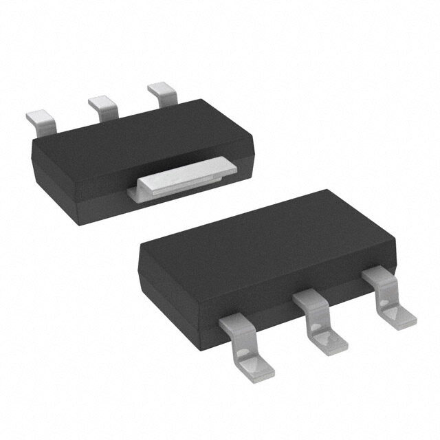
| 产品图片 |
|
| 产品型号 | BD46451G-TR |
| rohs | 无铅 / 符合限制有害物质指令(RoHS)规范要求 |
| 产品系列 | BD46xxx |
| 产品培训模块 | http://www.digikey.cn/PTM/IndividualPTM.page?site=cn&lang=zhs&ptm=30334 |
| 供应商器件封装 | 5-SSOP |
| 其它名称 | BD46451GDKR |
| 包装 | Digi-Reel® |
| 受监控电压数 | 1 |
| 复位 | 低有效 |
| 复位超时 | 最小为 90 ms |
| 安装类型 | 表面贴装 |
| 封装/外壳 | 6-TFSOP(0.063",1.60mm 宽),5 引线 |
| 工作温度 | -40°C ~ 105°C |
| 标准包装 | 1 |
| 电压-阈值 | 4.5V |
| 类型 | 简单复位/加电复位 |
| 输出 | 推挽式,图腾柱 |


- 商务部:美国ITC正式对集成电路等产品启动337调查
- 曝三星4nm工艺存在良率问题 高通将骁龙8 Gen1或转产台积电
- 太阳诱电将投资9.5亿元在常州建新厂生产MLCC 预计2023年完工
- 英特尔发布欧洲新工厂建设计划 深化IDM 2.0 战略
- 台积电先进制程称霸业界 有大客户加持明年业绩稳了
- 达到5530亿美元!SIA预计今年全球半导体销售额将创下新高
- 英特尔拟将自动驾驶子公司Mobileye上市 估值或超500亿美元
- 三星加码芯片和SET,合并消费电子和移动部门,撤换高东真等 CEO
- 三星电子宣布重大人事变动 还合并消费电子和移动部门
- 海关总署:前11个月进口集成电路产品价值2.52万亿元 增长14.8%


PDF Datasheet 数据手册内容提取
Datasheet Voltage Detector IC Series Counter Timer Built-in CMOS Voltage Detector IC BD45xxx series BD46xxx series ●General Description ●Key Specifications (cid:132) Detection voltage: 2.3V to 4.8V (Typ.) ROHM’s BD45xxx and BD46xxx series are highly 0.1V steps accurate, low current consumption Voltage Detector ICs. (cid:132) High accuracy detection voltage: ±1.0% Because the counter timer delay circuit is built into (cid:132) Ultra-low current consumption: 0.85µA (Typ.) these series, an external capacitor for the delay time (cid:132) Operating temperature range: -40°C to +105°C setting is unnecessary. The lineup was established with (cid:132) Three internal, fixed delay time: 50ms low output types (Nch open drain and CMOS output) 100ms and detection voltages range from 2.3V to 4.8V in 200ms increments of 0.1V, so that the series may be selected ●Package according the application at hand. SSOP5 2.90mm x 2.80mm x 1.25mm ●Features (cid:132) Counter Timer Built-in ●Applications (cid:132) No delay time setting external capacitor required Circuits using microcontrollers or logic circuits that (cid:132) Ultra-low current consumption require a reset. (cid:132) Two output types (Nch open drain and CMOS output) (cid:132) Package SSOP5 is similar to SOT-23-5 (JEDEC) ●Typical Application Circuit VDD1 VDD2 VDD1 RL BD45xxx R ST Mcoicnrtoro ller BD46xxx RST Mcoicnrtoroller C L C L (Noise-filtering (Noise-filtering Capacitor) Capacitor) GND GND (Open Drain Output Type) (CMOS Output Type) BD45xxx series BD46xxx series ●Connection Diagram ●Pin Descriptions SSOP5 VDD VOUT PIN No. Symbol Function 1 ER Manual Reset 2 SUB Substrate * 3 GND GND TOP VIEW Marking Lot. No 4 VOUT Reset Output ER SUB GND 5 VDD Power Supply Voltage *Connect the substrate to GND. ○Product structure:Silicon monolithic integrated circuit ○This product is not designed for protection against radioactive rays .w ww.rohm.com TSZ02201-0R7R0G300010-1-2 © 2013 ROHM Co., Ltd. All rights reserved. 1/13 TSZ22111・14・001 15.Nov.2013 Rev.007
DDaattaasshheeeett BD45xxx series BD46xxx series ●Ordering Information B D x x x x x x - T R Part Output Type Reset Voltage Value Counter Timer Package Packaging and Number 45 : Open Drain 23 : 2.3V Delay Time Settings G : SSOP5 forming specification 46 : CMOS 0.1V step 5 : 50ms TR : Embossed tape 48 : 4.8V 1 : 100ms and reel 2 : 200ms SSOP5 <Tape and Reel information> 2.9±0.2 4°+−64°° Tape Embossed carrier tape 5 4 Quantity 3000pcs ±2.80.2 +0.21.6−0.1 Min. Dofi rfeecetdion T(RTreheel odnir ethcetio lenf tis h tahned 1 apnind oyfo pur opduull cot uist tahte t htaep uep opne rt hrieg hritg whth heann ydou hold ) 1 2 3 0.2 0.13+−00..0053 1pin Max. S 1.25 +0.05 ±1.10.05 ±0.050.05 0.95 00.1.42S−0.04 Direction of feed (Unit : mm) Reel ∗ Order quantity needs to be multiple of the minimum quantity. ●Lineup Table 1. Open Drain Output Type Counter Timer Delay Time Settings 50ms 100ms 200ms Detection Part Part Part Marking Marking Marking Voltage Number Number Number 4.8V T0 BD45485 TS BD45481 UJ BD45482 4.7V T1 BD45475 TT BD45471 UK BD45472 4.6V T2 BD45465 TU BD45461 UL BD45462 4.5V T3 BD45455 TV BD45451 UM BD45452 4.4V T4 BD45445 TW BD45441 UN BD45442 4.3V T5 BD45435 TX BD45431 UP BD45432 4.2V T6 BD45425 TY BD45421 UQ BD45422 4.1V T7 BD45415 TZ BD45411 UR BD45412 4.0V T8 BD45405 U0 BD45401 US BD45402 3.9V T9 BD45395 U1 BD45391 UT BD45392 3.8V TA BD45385 U2 BD45381 UU BD45382 3.7V TB BD45375 U3 BD45371 UV BD45372 3.6V TC BD45365 U4 BD45361 UW BD45362 3.5V TD BD45355 U5 BD45351 UX BD45352 3.4V TE BD45345 U6 BD45341 UY BD45342 3.3V TF BD45335 U7 BD45331 UZ BD45332 3.2V TG BD45325 U8 BD45321 V0 BD45322 3.1V TH BD45315 U9 BD45311 V1 BD45312 3.0V TJ BD45305 UA BD45301 V2 BD45302 2.9V TK BD45295 UB BD45291 V3 BD45292 2.8V TL BD45285 UC BD45281 V4 BD45282 2.7V TM BD45275 UD BD45271 V5 BD45272 2.6V TN BD45265 UE BD45261 V6 BD45262 2.5V TP BD45255 UF BD45251 V7 BD45252 2.4V TQ BD45245 UG BD45241 V8 BD45242 2.3V TR BD45235 UH BD45231 V9 BD45232 www.rohm.com TSZ02201-0R7R0G300010-1-2 © 2013 ROHM Co., Ltd. All rights reserved. 2/13 TSZ22111・15・001 15.Nov.2013 Rev.007
DDaattaasshheeeett BD45xxx series BD46xxx series ●Lineup - continued Table 2. CMOS Output Type Counter Timer Delay Time Settings 50ms 100ms 200ms Detection Part Part Part Marking Marking Marking Voltage Number Number Number 4.8V VA BD46485 W2 BD46481 WU BD46482 4.7V VB BD46475 W3 BD46471 WV BD46472 4.6V VC BD46465 W4 BD46461 WW BD46462 4.5V VD BD46455 W5 BD46451 WX BD46452 4.4V VE BD46445 W6 BD46441 WY BD46442 4.3V VF BD46435 W7 BD46431 WZ BD46432 4.2V VG BD46425 W8 BD46421 X0 BD46422 4.1V VH BD46415 W9 BD46411 X1 BD46412 4.0V VJ BD46405 WA BD46401 X2 BD46402 3.9V VK BD46395 WB BD46391 X3 BD46392 3.8V VL BD46385 WC BD46381 X4 BD46382 3.7V VM BD46375 WD BD46371 X5 BD46372 3.6V VN BD46365 WE BD46361 X6 BD46362 3.5V VP BD46355 WF BD46351 X7 BD46352 3.4V VQ BD46345 WG BD46341 X8 BD46342 3.3V VR BD46335 WH BD46331 X9 BD46332 3.2V VS BD46325 WJ BD46321 XA BD46322 3.1V VT BD46315 WK BD46311 XB BD46312 3.0V VU BD46305 WL BD46301 XC BD46302 2.9V VV BD46295 WM BD46291 XD BD46292 2.8V VW BD46285 WN BD46281 XE BD46282 2.7V VX BD46275 WP BD46271 XF BD46272 2.6V VY BD46265 WQ BD46261 XG BD46262 2.5V VZ BD46255 WR BD46251 XH BD46252 2.4V W0 BD46245 WS BD46241 XJ BD46242 2.3V W1 BD46235 WT BD46231 XK BD46232 www.rohm.com TSZ02201-0R7R0G300010-1-2 © 2013 ROHM Co., Ltd. All rights reserved. 3/13 TSZ22111・15・001 15.Nov.2013 Rev.007
DDaattaasshheeeett BD45xxx series BD46xxx series (cid:122) Absolute maximum ratings Parameter Symbol Limits Unit Power Supply Voltage V -GND -0.3 to +10 V DD Nch Open Drain Output GND-0.3 to +10 Output Voltage VOUT V CMOS Output GND-0.3 to V +0.3 DD Output Current IO 60 mA ER pin Voltage VCT GND-0.3 to V +0.3 V DD Power Dissipation *1 *2 Pd 540 mW Operating Temperature Topr -40 to +105 °C Ambient Storage Temperature Tstg -55 to +125 °C *1 Reduced by 5.4mW/°C when used over 25°C. *2 When mounted on ROHM standard circuit board (70mm×70mm×1.6mm, glass epoxy board). ●Electrical characteristics (Unless Otherwise Specified Ta=-40 to 105°C) Limit Parameter Symbol Condition Unit Min. Typ. Max. VDD=H(cid:198)L, RL=470kΩ *1 VDET(T) VDET(T) VDET(T) ×0.99 ×1.01 Ta=+25°C 2.475 2.5 2.525 VDET=2.5V Ta=-40°C to 85°C 2.418 - 2.584 Ta=85°C to 105°C 2.404 - 2.597 Ta=+25°C 2.970 3.0 3.030 VDET=3.0V Ta=-40°C to 85°C 2.901 - 3.100 Ta=85°C to 105°C 2.885 - 3.117 Detection Voltage VDET Ta=+25°C 3.267 3.3 3.333 V VDET=3.3V Ta=-40°C to 85°C 3.191 - 3.410 Ta=85°C to 105°C 3.173 - 3.428 Ta=+25°C 4.158 4.2 4.242 VDET=4.2V Ta=-40°C to 85°C 4.061 - 4.341 Ta=85°C to 105°C 4.039 - 4.364 Ta=+25°C 4.752 4.8 4.848 VDET=4.8V Ta=-40°C to 85°C 4.641 - 4.961 Ta=85°C to 105°C 4.616 - 4.987 Detection Voltage VDET/ -40°C to +105°C - ±100 ±360 ppm/°C Temperature coefficient ∆T VDET(T) VDET(T) VDET(T) Hysteresis Voltage ∆VDET VDD=L(cid:198)H(cid:198)L, RL=470kΩ V ×0.03 ×0.05 ×0.08 ‘High’ Output CL=100pF, BD45XX5, BD46XX5 45 50 55 Delay time tPLH RL=100kΩ BD45XX1, BD46XX1 90 100 110 ms *1, *2, *3 BD45XX2, BD46XX2 180 200 220 VDD=VDET-0.2V, VER=0V VDET=2.3V to 3.1V *1 - 0.70 2.10 VDD=VDET-0.2V, VER=0V VDET=2.3V to 3.1V - 0.70 2.85 Circuit Current VDD=VDET-0.2V, VER=0V VDET=3.2V to 4.2V *1 - 0.75 2.25 IDD1 µA when ON VDD=VDET-0.2V, VER=0V VDET=3.2V to 4.2V - 0.75 3.00 VDD=VDET-0.2V, VER=0V VDET=4.3V to 4.8V *1 - 0.80 2.40 VDD=VDET-0.2V, VER=0V VDET=4.3V to 4.8V - 0.80 3.15 VDD=VDET+0.2V, VER=0V VDET=2.3V to 3.1V *1 - 0.75 2.25 VDD=VDET+0.2V, VER=0V VDET=2.3V to 3.1V - 0.75 4.28 Circuit Current VDD=VDET+0.2V, VER=0V VDET=3.2V to 4.2V *1 - 0.80 2.40 IDD2 µA when OFF VDD=VDET+0.2V, VER=0V VDET=3.2V to 4.2V - 0.80 4.50 VDD=VDET+0.2V, VER=0V VDET=4.3V to 4.8V *1 - 0.85 2.55 VDD=VDET+0.2V, VER=0V VDET=4.3V to 4.8V - 0.85 4.73 VDET(T):Standard Detection Voltage (2.3V to 4.8V, 0.1V step) RL :Pull-up resistor to be connected between VOUT and power supply. CL :Capacitor to be connected between VOUT and GND. *1 Guarantee is Ta=25°C. *2 tPLH:VDD=(VDET(T)-0.5V)(cid:198)(VDET(T)+0.5V) *3 tPLH:VDD=Please set the rise up time between VDD=0(cid:198)VDET to more than 100µs. Attention: Please connect the GND when you don’t use ‘ER’ www.rohm.com TSZ02201-0R7R0G300010-1-2 © 2013 ROHM Co., Ltd. All rights reserved. 4/13 TSZ22111・15・001 15.Nov.2013 Rev.007
DDaattaasshheeeett BD45xxx series BD46xxx series ●Electrical characteristics (Unless Otherwise Specified Ta=-40 to 105°C) - continued Limit Parameter Symbol Condition Unit Min. Typ. Max. VOL≤0.4V, RL=470kΩ, Ta=25 to 105°C 0.95 - - Operating Voltage Range VOPL V VOL≤0.4V, RL=470kΩ, Ta=-40 to 25°C 1.20 - - ‘High’ Output Voltage (Pch) VOH VDD=4.8V, ISOURCE= 1.0 mA, VDET(2.3V to 4.2V) VDD-0.5 - - V VDD=6.0V, ISOURCE= 1.2 mA, VDET(4.3V to 4.8V) VDD-0.5 - - ‘Low’Output Voltage (Nch) VOL VDD=1.2V, ISINK = 0.45 mA - - 0.3 V VDD=2.4V, ISINK = 1.3 mA, VDET(2.7V to 4.8V) - - 0.3 Leak Current when OFF Ileak VDD=VDS=10V *1 - - 0.1 µA ER Pin ‘H’ Voltage VEH *1 2.0 - - V ER Pin ‘L’ Voltage VEL *1 - - 0.8 V ER Pin Input Current IEL - 1 10 µA VDET(T):Standard Detection Voltage (2.3V to 4.8V, 0.1V step) RL :Pull-up resistor to be connected between VOUT and power supply. CL :Capacitor to be connected between VOUT and GND. *1 Guarantee is Ta=25°C. Attention: Please connect the GND when you don’t use ‘ER’ www.rohm.com TSZ02201-0R7R0G300010-1-2 © 2013 ROHM Co., Ltd. All rights reserved. 5/13 TSZ22111・15・001 15.Nov.2013 Rev.007
DDaattaasshheeeett BD45xxx series BD46xxx series ●Block Diagrams VDD VOUT Oscillation Circuit Counter Timer Vref GND ER Fig.1 BD45xxx Series VDD Oscillation Circuit Counter Timer VOUT Vref GND ER Fig.2 BD46xxx Series www.rohm.com TSZ02201-0R7R0G300010-1-2 © 2013 ROHM Co., Ltd. All rights reserved. 6/13 TSZ22111・15・001 15.Nov.2013 Rev.007
DDaattaasshheeeett BD45xxx series BD46xxx series ●Typical Performance Curves 2.0 20 A] 【B【BDD4545228811】G 】 mA] 【【BBDD4455228811】G】 μ [L [DD 1.5 【BD46281】 : IO 15 【BD46281】 : I T T EN EN RR VDD=2.4V RR 1.0 CU 10 CU T T PU CUI 0.5 UT 5 R O CI W" VDD=1.2V O 0.0 L 0 " 0 1 2 3 4 5 6 7 8 9 10 0.0 0.5 1.0 1.5 2.0 2.5 VDD SUPPLY VOLTAGE :VDD[V] DRAIN-SOURCE VOLTAGE : VDS[V] Fig.3 Circuit Current Fig.4 “Low” Output Current 20 7 A] m 【【BBDD4466228811】G 】 【B【DB4D52458412】1G 】 :T I[OH 15 VDD=6.0V V[V]OUT 56 【BD46281】 EN :E R G 4 R A T CU 10 VDD=4.8V VOLT 3 Ta=25℃ OUTPU 5 TPUT 2 U H" O 1 Ta=25℃ G HI 0 0 " 0 1 2 3 4 5 6 0 0.5 1 1.5 2 2.5 3 3.5 4 4.5 5 5.5 DRAIN-SOURCE VOLTAGE : VDS[V] VDD SUPPLY VOLTAGE :VDD[V] Fig.5 “High” Output Current Fig.6 I/O Characteristics www.rohm.com TSZ02201-0R7R0G300010-1-2 © 2013 ROHM Co., Ltd. All rights reserved. 7/13 TSZ22111・15・001 15.Nov.2013 Rev.007
DDaattaasshheeeett BD45xxx series BD46xxx series ●Typical Performance Curves – continued 20 20 【【BDBD4542682811】G 】 【【BBDD4455442211G】】 V] A] :E V[OUT 15 【BD46281】 :T I[μER 15 【BD46421】 G N A E T 10 R 10 L R O U V C T S PU 5 BIA 5 UT R O E 0 0 0 1 2 3 4 5 6 7 8 9 10 0 1 2 3 4 5 6 7 8 9 10 ER VOLTAGE : VER[V] ER VOLTAGE : VER[V] Fig.7 ER Terminal Threshold Voltage Fig.8 ER Terminal Input Current 5.8 1.6 [V]DET 5.4 【BD45421】【【BBDD4456442211G】】 [μA]DD1 1.4 【【BBDD4455442211】G】 :OLTAGE V 45..60 Low to high(VDET+ΔVDET) WHEN ONI: 011...802 【BD46421】 V 4.2 T N EN 0.6 O R TI 3.8 High to low(VDET) UR 0.4 C C ETE 3.4 UIT 0.2 D C ~ R 3.0 CI 0.0 -40 0 40 80 -40 -20 0 20 40 60 80 100 TEMPERATURE : Ta[℃] TEMPERATURE : Ta[℃] Fig.9 Detection Voltage Fig.10 Circuit Current when ON Release Voltage (VDET-0.2V) www.rohm.com TSZ02201-0R7R0G300010-1-2 © 2013 ROHM Co., Ltd. All rights reserved. 8/13 TSZ22111・15・001 15.Nov.2013 Rev.007
DDaattaasshheeeett BD45xxx series BD46xxx series ●Typical Performance Curves – continued 3.0 1.5 :OFF I[μA]DD2 122222......802468 【【【BBBDDD444565444222111】】G】 OLTAGE: V[V]OPL 1.0 【【BBDD4456442211】】 N V HE 1.6 NG NT W 11..24 RATI RE 1.0 PE 0.5 R O UIT CU 000...468 NIMUM RC 0.2 MI CI 0.0 0.0 -40 -20 0 20 40 60 80 100 -40 -20 0 20 40 60 80 100 TEMPERATURE : Ta[℃] TEMPERATURE : Ta[℃] Fig.11 Circuit Current when OFF Fig.12 Operating Limit Voltage 250 50 :ELAY TIME t[msec]DELAY TIME : t [ms] PLHPLH 112050000 【【BBDD44552288【21】】【【BDBBBBDD4DD445662442285588□2221】】88G21 GG】 :ELAY TIME t[μsec]W” DELAY TIME : t [µs] PHLPLH 234000 【B【【D4BB5DD244856122G88 t11PH】】L】 H" DHIGH” 50 W" D“LO 10 HIG“ 【BD45285】【BBDD464258258】5 G LO " " 0 0 -60 -40 -20 0 20 40 60 80 100 120 -60 -40 -20 0 20 40 60 80 100 120 TEMPERATURE : Ta[℃] TEMPERATURE : Ta[℃] Fig.13 Output Delay Time Fig.14 Output Delay Time “Low”(cid:198)”High” “High”(cid:198)”Low” www.rohm.com TSZ02201-0R7R0G300010-1-2 © 2013 ROHM Co., Ltd. All rights reserved. 9/13 TSZ22111・15・001 15.Nov.2013 Rev.007
DDaattaasshheeeett BD45xxx series BD46xxx series ●Application Information Explanation of Operation For both the open drain type (Fig.15) and the CMOS output type (Fig.16), the detection and release voltages are used as threshold voltages. When the voltage applied to the V pins reaches the applicable threshold voltage, the V terminal DD OUT voltage switches from either “High” to “Low” or from “Low” to “High”. Because the BD45xxx series uses an open drain output type, it is necessary to connect either a pull-up resistor to V or another power supply if needed [The output “High” voltage DD (V ) in this case becomes V or the voltage of the other power supply]. OUT DD VDD VDD VDD R1 R1 Vref Vref Q2 Reset Oscillation VOUT Oscillation R2 Circuit Counter R2 Circuit Counter Reset Timer Q1 Timer VOUT R3 R3 Q1 GND GND ER ER Fig.15 (BD45xxx Type Internal Block Diagram) Fig.16 (BD46xxx Type Internal Block Diagram) Reference Data Examples of Leading (t ) and Falling (t ) Output PLH PHL Part Number t [ms] t [µs] PLH PHL BD45275G 50 18 BD46275G 50 18 VDD=2.2V(cid:198)3.2V VDD=3.2V(cid:198)2.2V *This data is for reference only. The figures will vary with the application, so please confirm actual operating conditions before use. Timing Waveform Example: The following shows the relationship between the input voltages V , the output voltage V and ER terminal when DD OUT the input power supply voltage V is made to sweep up and sweep down (the circuits are those in Fig. 12 and 13). DD 1 When the power supply is turned on, the output is unstable from VDD after over the operating limit voltage (V ) until t . Therefore it is OPL PHL VDET+ΔVDET possible that the reset signal is not outputted when the rise time of VDD VDET ⑦ V is faster than t . VOPL DD PHL 0V 2 When V is greater than V but less than the reset release DD OPL voltage (V + ∆V ), the output voltages will switch to Low. VOH DET DET tPLH tPLH tPLH 3 If VDD exceeds the reset release voltage (VDET + ∆VDET), the VOUT tPHL counter timer start and VOUT switches from L to H. VOL tPHL 4 When more than the high level voltage is supplied to the ER terminal, V comes to “L” after t delay time. Therefore, a time OUT PLH VEH when ER terminal is “H” is necessary for 100µsec or more. ER tPHL 5 When the ER terminal switches to Low, the counter timer starts to operate, a delay of t occurs, and V switches from “L” to “H”. PLH OUT 6 If V drops below the detection voltage (V ) when the power ① ② ③ ④ ⑤ ⑥ DD DET Fig.17 Timing Waveform supply is powered down or when there is a power supply fluctuation, VOUT switches to L (with a delay of tPHL). 7 The potential difference between the detection voltage and the release voltage is known as the hysteresis width (∆V ). The DET system is designed such that the output does not toggle with power supply fluctuations within this hysteresis width, preventing malfunctions due to noise. These time changes by the application and use it, please verify and confirm using practical applications. www.rohm.com TSZ02201-0R7R0G300010-1-2 © 2013 ROHM Co., Ltd. All rights reserved. 10/13 TSZ22111・15・001 15.Nov.2013 Rev.007
DDaattaasshheeeett BD45xxx series BD46xxx series ●Circuit Applications 1) Examples of common power supply detection reset circuits. VDD1 VDD2 Application examples of BD45xxx series (Open Drain output type) and BD46xxx series (CMOS output type) RL are shown below. Micro BD45xxx RST controller CASE1: Power supply of the microcontroller (VDD2) differs from the power supply of the reset detection C L (VDD1). (Noise-filtering Use an open drain output type (BD45xxx) with a load Capacitor) GND resistance RL as shown Fig.18. Fig.18 Open Drain Output Type CASE2: Power supply of the microcontroller (V ) is DD1 same as the power supply of the reset detection (V ). DD1 VDD1 Use a CMOS output type (BD46xxx) device or an open drain output type (BD45xxx) device with a pull up resistor between the output and V . DD1 BD46xxx RST Mcoicnrtoro ller When a capacitance C for noise filtering is connected to L the V pin (the reset signal input terminal of the OUT C L microcontroller), please take into account the waveform (Noise-filtering of the rise and fall of the output voltage (V ). Capacitor) OUT GND Fig.19 CMOS Output Type 2) The following is an example of a circuit application in which an OR connection between two types of detection voltage resets the microcontroller. VDD1 V DD2 V DD3 RL Micro BD45xxx BD45xxx RST controller GND Fig. 20 To reset the microcontroller when many independent power supplies are used in the system, OR connect an open drain output type (BD45xxx series) to the microcontroller’s input with pull-up resistor to the supply voltage of the microcontroller (V ) as shown in Fig. 20. By pulling-up to V , output “High” voltage of micro-controller power supply is possible. DD3 DD3 www.rohm.com TSZ02201-0R7R0G300010-1-2 © 2013 ROHM Co., Ltd. All rights reserved. 11/13 TSZ22111・15・001 15.Nov.2013 Rev.007
DDaattaasshheeeett BD45xxx series BD46xxx series 3) Examples of the power supply with resistor dividers. In applications wherein the power supply voltage of an IC comes from a resistor divider circuit, an in-rush current will flow into the circuit when the output level switches from “High” to “Low” or vice versa. In-rush current is a sudden surge of current that flows from the power supply (VDD) to ground (GND) as the output logic changes its state. This current flow may cause malfunction in the systems operation such as output oscillations, etc. V1 R2 I1 VDD R1 BD45xxx VOUT CIN BD46xxx CL GND Fig. 21 When an in-rush current (I1) flows into the circuit (Refer to Fig. 21) at the time when output switches from “Low” to “High”, a voltage drop of I1×R2 (input resistor) will occur in the circuit causing the VDD supply voltage to decrease. When the VDD voltage drops below the detection voltage, the output will switch from “High” to “Low”. While the output voltage is at “Low” condition, in-rush current will stop flowing and the voltage drop will be reduced. As a result, the output voltage will switches again from “Low” to “High” which causes an in-rush current and a voltage drop. This operation repeats and will result to oscillation. IDD In-rush Current VDD 0 VDET Fig. 22 Current Consumption vs. Power Supply Voltage www.rohm.com TSZ02201-0R7R0G300010-1-2 © 2013 ROHM Co., Ltd. All rights reserved. 12/13 TSZ22111・15・001 15.Nov.2013 Rev.007
DDaattaasshheeeett BD45xxx series BD46xxx series ●Operational Notes 1) Absolute maximum ratings Operating the IC over the absolute maximum ratings may damage the IC. The damage can either be a short circuit between pins or an open circuit between pins. Therefore, it is important to consider circuit protection measures, such as adding a fuse, in case the IC is operated over the absolute maximum ratings. 2) Ground Voltage The voltage of the ground pin must be the lowest voltage of all pins of the IC at all operating conditions. Ensure that no pins are at a voltage below the ground pin at any time, even during transient condition. 3) Recommended operating conditions These conditions represent a range within which the expected characteristics of the IC can be approximately obtained. The electrical characteristics are guaranteed under the conditions of each parameter. 4) Bypass Capacitor for Noise Rejection To help reject noise, put a 1µF capacitor between VDD pin and GND and 1000pF capacitor between VOUT pin and GND. Be careful when using extremely big capacitor as transient response will be affected. 5) Short between pins and mounting errors Be careful when mounting the IC on printed circuit boards. The IC may be damaged if it is mounted in a wrong orientation or if pins are shorted together. Short circuit may be caused by conductive particles caught between the pins. 6) Operation under strong electromagnetic field Operating the IC in the presence of a strong electromagnetic field may cause the IC to malfunction. 7) The V line impedance might cause oscillation because of the detection current. DD 8) A VDD to GND capacitor (as close connection as possible) should be used in high VDD line impedance condition. 9) Lower than the mininum input voltage puts the VOUT in high impedance state, and it must be VDD in pull up (VDD) condition. 10) This IC has extremely high impedance terminals. Small leak current due to the uncleanness of PCB surface might cause unexpected operations. Application values in these conditions should be selected carefully. If the leakage of about 1MΩ is assumed between the ER terminal and the GND terminal, 100kΩ connection between the ER terminal and the V terminal would be recommended. If the leakage is assumed between the V terminal and the GND DD OUT terminal, the pull-up resistor should be less than 1/10 of the assumed leak resistance. 11) External parameters The recommended parameter range for RL is 50kΩ to 1MΩ. There are many factors (board layout, etc) that can affect characteristics. Please verify and confirm using practical applications. 12) Power on reset operation Please note that the power on reset output varies with the V rise time. Please verify the behavior in the actual DD operation. 13) Testing on application boards When testing the IC on an application board, connecting a capacitor directly to a low-impedance output pin may subject the IC to stress. Always discharge capacitors completely after each process or step. The IC’s power supply should always be turned off completely before connecting or removing it from the test setup during the inspection process. To prevent damage from static discharge, ground the IC during assembly and use similar precautions during transport and storage. 14) Rush current When power is first supplied to the IC, rush current may flow instantaneously. It is possible that the charge current to the parasitic capacitance of internal photo diode or the internal logic may be unstable. Therefore, give special consideration to power coupling capacitance, power wiring, width of GND wiring, and routing of connections. www.rohm.com TSZ02201-0R7R0G300010-1-2 © 2013 ROHM Co., Ltd. All rights reserved. 13/13 TSZ22111・15・001 15.Nov.2013 Rev.007
DDaattaasshheeeett Notice Precaution on using ROHM Products 1. Our Products are designed and manufactured for application in ordinary electronic equipments (such as AV equipment, OA equipment, telecommunication equipment, home electronic appliances, amusement equipment, etc.). If you intend to use our Products in devices requiring extremely high reliability (such as medical equipment (Note 1), transport equipment, traffic equipment, aircraft/spacecraft, nuclear power controllers, fuel controllers, car equipment including car accessories, safety devices, etc.) and whose malfunction or failure may cause loss of human life, bodily injury or serious damage to property (“Specific Applications”), please consult with the ROHM sales representative in advance. Unless otherwise agreed in writing by ROHM in advance, ROHM shall not be in any way responsible or liable for any damages, expenses or losses incurred by you or third parties arising from the use of any ROHM’s Products for Specific Applications. (Note1) Medical Equipment Classification of the Specific Applications JAPAN USA EU CHINA CLASSⅢ CLASSⅡb CLASSⅢ CLASSⅢ CLASSⅣ CLASSⅢ 2. ROHM designs and manufactures its Products subject to strict quality control system. However, semiconductor products can fail or malfunction at a certain rate. Please be sure to implement, at your own responsibilities, adequate safety measures including but not limited to fail-safe design against the physical injury, damage to any property, which a failure or malfunction of our Products may cause. The following are examples of safety measures: [a] Installation of protection circuits or other protective devices to improve system safety [b] Installation of redundant circuits to reduce the impact of single or multiple circuit failure 3. Our Products are designed and manufactured for use under standard conditions and not under any special or extraordinary environments or conditions, as exemplified below. Accordingly, ROHM shall not be in any way responsible or liable for any damages, expenses or losses arising from the use of any ROHM’s Products under any special or extraordinary environments or conditions. If you intend to use our Products under any special or extraordinary environments or conditions (as exemplified below), your independent verification and confirmation of product performance, reliability, etc, prior to use, must be necessary: [a] Use of our Products in any types of liquid, including water, oils, chemicals, and organic solvents [b] Use of our Products outdoors or in places where the Products are exposed to direct sunlight or dust [c] Use of our Products in places where the Products are exposed to sea wind or corrosive gases, including Cl2, H2S, NH3, SO2, and NO2 [d] Use of our Products in places where the Products are exposed to static electricity or electromagnetic waves [e] Use of our Products in proximity to heat-producing components, plastic cords, or other flammable items [f] Sealing or coating our Products with resin or other coating materials [g] Use of our Products without cleaning residue of flux (even if you use no-clean type fluxes, cleaning residue of flux is recommended); or Washing our Products by using water or water-soluble cleaning agents for cleaning residue after soldering [h] Use of the Products in places subject to dew condensation 4. The Products are not subject to radiation-proof design. 5. Please verify and confirm characteristics of the final or mounted products in using the Products. 6. In particular, if a transient load (a large amount of load applied in a short period of time, such as pulse. is applied, confirmation of performance characteristics after on-board mounting is strongly recommended. Avoid applying power exceeding normal rated power; exceeding the power rating under steady-state loading condition may negatively affect product performance and reliability. 7. De-rate Power Dissipation (Pd) depending on Ambient temperature (Ta). When used in sealed area, confirm the actual ambient temperature. 8. Confirm that operation temperature is within the specified range described in the product specification. 9. ROHM shall not be in any way responsible or liable for failure induced under deviant condition from what is defined in this document. Precaution for Mounting / Circuit board design 1. When a highly active halogenous (chlorine, bromine, etc.) flux is used, the residue of flux may negatively affect product performance and reliability. 2. In principle, the reflow soldering method must be used; if flow soldering method is preferred, please consult with the ROHM representative in advance. For details, please refer to ROHM Mounting specification Notice - GE Rev.002 © 2014 ROHM Co., Ltd. All rights reserved.
DDaattaasshheeeett Precautions Regarding Application Examples and External Circuits 1. If change is made to the constant of an external circuit, please allow a sufficient margin considering variations of the characteristics of the Products and external components, including transient characteristics, as well as static characteristics. 2. You agree that application notes, reference designs, and associated data and information contained in this document are presented only as guidance for Products use. Therefore, in case you use such information, you are solely responsible for it and you must exercise your own independent verification and judgment in the use of such information contained in this document. ROHM shall not be in any way responsible or liable for any damages, expenses or losses incurred by you or third parties arising from the use of such information. Precaution for Electrostatic This Product is electrostatic sensitive product, which may be damaged due to electrostatic discharge. Please take proper caution in your manufacturing process and storage so that voltage exceeding the Products maximum rating will not be applied to Products. Please take special care under dry condition (e.g. Grounding of human body / equipment / solder iron, isolation from charged objects, setting of Ionizer, friction prevention and temperature / humidity control). Precaution for Storage / Transportation 1. Product performance and soldered connections may deteriorate if the Products are stored in the places where: [a] the Products are exposed to sea winds or corrosive gases, including Cl2, H2S, NH3, SO2, and NO2 [b] the temperature or humidity exceeds those recommended by ROHM [c] the Products are exposed to direct sunshine or condensation [d] the Products are exposed to high Electrostatic 2. Even under ROHM recommended storage condition, solderability of products out of recommended storage time period may be degraded. It is strongly recommended to confirm solderability before using Products of which storage time is exceeding the recommended storage time period. 3. Store / transport cartons in the correct direction, which is indicated on a carton with a symbol. Otherwise bent leads may occur due to excessive stress applied when dropping of a carton. 4. Use Products within the specified time after opening a humidity barrier bag. Baking is required before using Products of which storage time is exceeding the recommended storage time period. Precaution for Product Label QR code printed on ROHM Products label is for ROHM’s internal use only. Precaution for Disposition When disposing Products please dispose them properly using an authorized industry waste company. Precaution for Foreign Exchange and Foreign Trade act Since our Products might fall under controlled goods prescribed by the applicable foreign exchange and foreign trade act, please consult with ROHM representative in case of export. Precaution Regarding Intellectual Property Rights 1. All information and data including but not limited to application example contained in this document is for reference only. ROHM does not warrant that foregoing information or data will not infringe any intellectual property rights or any other rights of any third party regarding such information or data. ROHM shall not be in any way responsible or liable for infringement of any intellectual property rights or other damages arising from use of such information or data.: 2. No license, expressly or implied, is granted hereby under any intellectual property rights or other rights of ROHM or any third parties with respect to the information contained in this document. Other Precaution 1. This document may not be reprinted or reproduced, in whole or in part, without prior written consent of ROHM. 2. The Products may not be disassembled, converted, modified, reproduced or otherwise changed without prior written consent of ROHM. 3. In no event shall you use in any way whatsoever the Products and the related technical information contained in the Products or this document for any military purposes, including but not limited to, the development of mass-destruction weapons. 4. The proper names of companies or products described in this document are trademarks or registered trademarks of ROHM, its affiliated companies or third parties. Notice - GE Rev.002 © 2014 ROHM Co., Ltd. All rights reserved.
DDaattaasshheeeett General Precaution 1. Before you use our Products, you are requested to carefully read this document and fully understand its contents. ROHM shall not be in any way responsible or liable for failure, malfunction or accident arising from the use of a ny ROHM’s Products against warning, caution or note contained in this document. 2. All information contained in this document is current as of the issuing date and subj ect to change without any prior notice. Before purchasing or using ROHM’s Products, please confirm the latest information with a ROHM sale s representative. 3. The information contained in this document is provided on an “as is” basis and ROHM does not warrant that all information contained in this document is accurate an d/or error-free. ROHM shall not be in any way responsible or liable for any damages, expenses or losses incurred by you or third parties resulting from inaccuracy or errors of or concerning such information. Notice – WE Rev.001 © 2014 ROHM Co., Ltd. All rights reserved.
Mouser Electronics Authorized Distributor Click to View Pricing, Inventory, Delivery & Lifecycle Information: R OHM Semiconductor: BD45231G-TR BD45232G-TR BD45235G-TR BD45241G-TR BD45242G-TR BD45245G-TR BD45251G-TR BD45252G-TR BD45255G-TR BD45261G-TR BD45262G-TR BD45265G-TR BD45271G-TR BD45272G-TR BD45275G-TR BD45281G-TR BD45282G-TR BD45285G-TR BD45291G-TR BD45292G-TR BD45295G-TR BD45301G-TR BD45302G-TR BD45305G-TR BD45311G-TR BD45312G-TR BD45315G-TR BD45321G-TR BD45322G-TR BD45325G-TR BD45331G-TR BD45332G-TR BD45335G-TR BD45341G-TR BD45342G-TR BD45345G-TR BD45351G-TR BD45352G-TR BD45355G-TR BD45361G-TR BD45362G-TR BD45365G-TR BD45371G-TR BD45372G-TR BD45375G-TR BD45381G-TR BD45382G-TR BD45385G-TR BD45391G-TR BD45392G-TR BD45395G-TR BD45401G-TR BD45402G-TR BD45405G-TR BD45411G-TR BD45412G-TR BD45415G-TR BD45421G-TR BD45422G-TR BD45425G-TR BD45431G-TR BD45432G-TR BD45435G-TR BD45441G-TR BD45442G-TR BD45445G-TR BD45451G-TR BD45452G-TR BD45455G-TR BD45461G-TR BD45462G-TR BD45465G-TR BD45471G-TR BD45472G-TR BD45475G-TR BD45481G-TR BD45482G-TR BD45485G-TR BD46231G-TR BD46232G-TR BD46235G-TR BD46241G-TR BD46242G-TR BD46245G-TR BD46251G-TR BD46252G-TR BD46255G-TR BD46261G-TR BD46262G-TR BD46265G-TR BD46271G-TR BD46272G-TR BD46275G-TR BD46281G-TR BD46282G-TR BD46285G-TR BD46291G-TR BD46292G-TR BD46295G-TR BD46301G-TR