ICGOO在线商城 > 集成电路(IC) > PMIC - 稳压器 - 线性 > BD25IC0WEFJ-E2
 Datasheet下载
- 型号: BD25IC0WEFJ-E2
- 制造商: ROHM Semiconductor
- 库位|库存: xxxx|xxxx
- 要求:
| 数量阶梯 | 香港交货 | 国内含税 |
| +xxxx | $xxxx | ¥xxxx |
查看当月历史价格
查看今年历史价格
BD25IC0WEFJ-E2产品简介:
ICGOO电子元器件商城为您提供BD25IC0WEFJ-E2由ROHM Semiconductor设计生产,在icgoo商城现货销售,并且可以通过原厂、代理商等渠道进行代购。 BD25IC0WEFJ-E2价格参考¥1.22-¥2.11。ROHM SemiconductorBD25IC0WEFJ-E2封装/规格:PMIC - 稳压器 - 线性, Linear Voltage Regulator IC Positive Fixed 1 Output 2.5V 1A 8-HTSOP-J。您可以下载BD25IC0WEFJ-E2参考资料、Datasheet数据手册功能说明书,资料中有BD25IC0WEFJ-E2 详细功能的应用电路图电压和使用方法及教程。
Rohm Semiconductor的BD25IC0WEFJ-E2是一款线性稳压器(LDO),属于电源管理集成电路(PMIC)的一部分。该器件主要应用于需要稳定、低噪声电源的电子系统中。

其典型应用场景包括:

1. 消费类电子产品:如智能手机、平板电脑、可穿戴设备等,用于为处理器、传感器或其他低电压电路提供稳定电源。
2. 车载电子系统:适用于车载导航、音响系统、摄像头模块等,满足汽车环境中对电源稳定性和可靠性的高要求。
3. 工业控制系统:用于工业自动化设备、传感器模块、PLC等,提供高精度、低纹波的电源。
4. 通信设备:如无线基站、路由器、光模块等,适用于对噪声敏感的射频和模拟电路供电。
5. 便携式仪器:如测量仪表、医疗设备等,因其低功耗和高稳定性,适合电池供电系统使用。

该稳压器具有低静态电流、良好的负载和线路瞬态响应特性,支持宽输入电压范围,并具备过热和过流保护功能,适用于对电源质量要求较高的中低功率应用场景。
| 参数 | 数值 |
| 产品目录 | 集成电路 (IC) |
| 描述 | IC REG LDO 2.5V 1A 8HTSOP-J |
| 产品分类 | |
| 品牌 | Rohm Semiconductor |
| 数据手册 | |
| 产品图片 |
|
| 产品型号 | BD25IC0WEFJ-E2 |
| rohs | 无铅 / 符合限制有害物质指令(RoHS)规范要求 |
| 产品系列 | - |
| 产品培训模块 | http://www.digikey.cn/PTM/IndividualPTM.page?site=cn&lang=zhs&ptm=30333 |
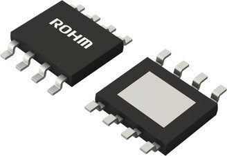
| 供应商器件封装 | 8-HTSOP-J |
| 其它名称 | BD25IC0WEFJ-E2TR |
| 包装 | 带卷 (TR) |
| 安装类型 | 表面贴装 |
| 封装/外壳 | 8-SOIC(0.154",3.90mm 宽)裸焊盘 |
| 工作温度 | -25°C ~ 85°C |
| 标准包装 | 2,500 |
| 特色产品 | http://www.digikey.cn/product-highlights/cn/zh/rohm-ba-bd-ldo-regulator-ics/3995 |
| 电压-跌落(典型值) | 0.4V @ 1A |
| 电压-输入 | 最高 5.5V |
| 电压-输出 | 2.5V |
| 电流-输出 | 1A |
| 电流-限制(最小值) | - |
| 稳压器拓扑 | 正,固定式 |
| 稳压器数 | 1 |


- 商务部:美国ITC正式对集成电路等产品启动337调查
- 曝三星4nm工艺存在良率问题 高通将骁龙8 Gen1或转产台积电
- 太阳诱电将投资9.5亿元在常州建新厂生产MLCC 预计2023年完工
- 英特尔发布欧洲新工厂建设计划 深化IDM 2.0 战略
- 台积电先进制程称霸业界 有大客户加持明年业绩稳了
- 达到5530亿美元!SIA预计今年全球半导体销售额将创下新高
- 英特尔拟将自动驾驶子公司Mobileye上市 估值或超500亿美元
- 三星加码芯片和SET,合并消费电子和移动部门,撤换高东真等 CEO
- 三星电子宣布重大人事变动 还合并消费电子和移动部门
- 海关总署:前11个月进口集成电路产品价值2.52万亿元 增长14.8%


PDF Datasheet 数据手册内容提取
Datasheet 1A Variable / Fixed Output LDO Regulators BDxxIC0WEFJ / BDxxIC0WHFV ●General Description BDxxIC0W series devices are LDO regulators with an output current of 1.0A. The output accuracy is ±1% of the output voltage. Both fixed and variable output voltage devices are available. The output voltage of the variable output voltage device can be varied from 0.8 to 4.5V using external resistors. Various fixed output voltage devices that do not use external resistors are also available. These LDO regulators are available in two package types: HTSOP-J8 (4.90mm x 6.00mm x 1.00mm) and HVSOF6 (1.60mm x 3.00mm x 0.75mm), and can be used in a wide variety of digital appliances. These devices have built in over current protection to protect the device when output is shorted, 0µA shutdown mode and thermal shutdown circuit to protect the device during over load conditions. These LDO regulators are usable with ceramic capacitors that enable a smaller layout and longer life. ●Features ●Package (Typ.) (Typ.) (Max.) +/-1% output voltage accuracy HTSOP-J8 4.90mm x 6.00mm x 1.00mm Built-in Over Current Protection circuit (OCP) HVSOF6 1.60mm x 3.00mm x 0.75mm Built-in Thermal Shut Down circuit (TSD) Zero µA Shutdown mode ●Key Specifications ■ Input Power Supply Voltage range: 2.4V to 5.5V ■ Output Voltage range(Variable type): 0.8V to 4.5V ■ Output Voltage(Fixed type): 1.0V/1.2V/1.25V/1.5V 1.8V/2.5V/2.6V/3.0V/3.3V (1.25V/2.6V:HVSOF6 only) ■ Output Current: 1.0A (Max.) ■ Shutdown Current: 0 µA (Typ.) ■ Operating Temperature Range: -25 to +85℃ HTSOP-J8 HVSOF6 ●Typical Application Circuit VCC VO VCC VO CIN R1 COUT CIN VO_S COUT EN FB EN R2 GND FIN GND FIN CIN,COUT : Ceramic Capacitor CIN,COUT : Ceramic Capacitor Output voltage variable type Output voltage fixed type ○Product structure:Silicon monolithic integrated circuit ○This product is not designed with protection against radioactive rays. www.rohm.com TSZ02201-GAG0A600030-1-2 © 2015 ROHM Co., Ltd. All rights reserved. 1/23 TSZ22111・14・001 19.Aug.2015 Rev.004
BDxxIC0WEFJ / BDxxIC0WHFV Datasheet ●Ordering Information B D x x I C 0 W y y y - z z Part Output Input Output Shutdown Package Packaging and forming specification Number voltage voltage current mode range 00:Variable :7V C0:1.0A “W”:included EFJ : HTSOP-J8 E2 : Emboss tape reel(HTSOP-J8) 10:1.0V HFV : HVSOF6 GTR : Emboss tape reel(HVSOF6) 12:1.2V 1C:1.25V 15:1.5V 18:1.8V 25:2.5V 26:2.6V 30:3.0V 33:3.3V www.rohm.com TSZ02201-GAG0A600030-1-2 © 2015 ROHM Co., Ltd. All rights reserved. 2/23 TSZ22111・15・001 19.Aug.2015 Rev.004
BDxxIC0WEFJ / BDxxIC0WHFV Datasheet ●Block Diagram BD00IC0WEFJ / BD00IC0WHFV (Variable output voltage type) V CC OCP SOFT START V O FB EN TSD GND Fig.1 Block Diagram ●Pin Configuration and Pin Description (HTSOP-J8) Pin No. Pin name Pin Function 1 VO Output pin 2 FB Feedback pin VO 1 8 VCC 3 GND GND pin FB 2 7 N.C 4 N.C No Connect (Connect to GND or leave OPEN) 5 EN Enable pin GND 3 6 N.C 6 N.C No Connect (Connect to GND or leave OPEN) N.C 4 5 EN 7 N.C No Connect (Connect to GND or leave OPEN) 8 VCC Input pin Reverse FIN Substrate (Connect to GND) (HVSOF6) Pin No. Pin name Pin Function 1 VO Output pin Vo 1 6 Vcc 2 FB Feedback pin 3 GND GND pin FB 2 5 N.C 4 EN Enable pin 5 N.C No Connect (Connect to GND or leave OPEN) GND 3 4 EN 6 VCC Input pin Reverse FIN Substrate (Connect to GND) www.rohm.com TSZ02201-GAG0A600030-1-2 © 2015 ROHM Co., Ltd. All rights reserved. 3/23 TSZ22111・15・001 19.Aug.2015 Rev.004
BDxxIC0WEFJ / BDxxIC0WHFV Datasheet ●Block Diagram BDxxIC0WEFJ / BDxxIC0WHFV (Fixed output voltage type) V CC OCP SOFT START V O EN TSD V O_S GND Fig.2 Block Diagram ●Pin Configuration and Pin Description (HTSOP-J8) Pin No. Pin name Pin Function 1 VO Output pin 2 VO_S Output voltage monitor pin VO 1 8 VCC 3 GND GND pin VO_S 2 7 N.C 4 N.C No Connect (Connect to GND or leave OPEN) 5 EN Enable pin GND 3 6 N.C 6 N.C No Connect (Connect to GND or leave OPEN) N.C 4 5 EN 7 N.C No Connect (Connect to GND or leave OPEN) 8 VCC Input pin Reverse FIN Substrate (Connect to GND) (HVSOF6) Pin No. Pin name Pin Function 1 VO Output pin 2 VO_S Output voltage monitor pin VO 1 6 VCC 3 GND GND pin VO_S 2 5 N.C 4 EN Enable pin 5 N.C No Connect (Connect to GND or leave OPEN) GND 3 4 EN 6 VCC Input pin Reverse FIN Substrate (Connect to GND) www.rohm.com TSZ02201-GAG0A600030-1-2 © 2015 ROHM Co., Ltd. All rights reserved. 4/23 TSZ22111・15・001 19.Aug.2015 Rev.004
BDxxIC0WEFJ / BDxxIC0WHFV Datasheet ●Absolute Maximum Ratings (Ta=25℃) Parameter Symbol Ratings Unit Power supply voltage VCC -0.3 to 7.0 *1 V EN voltage VEN -0.3 to 7.0 V HTSOP-J8 Pd 2.11 *2 W Power dissipation HVSOF6 Pd 1.70 *3 W Operating Temperature Range Topr -25 to +85 ℃ Storage Temperature Range Tstg -55 to +150 ℃ Junction Temperature Tjmax +150 ℃ *1 Not to exceed Pd *2 Reduced by 16.9mW/℃ for each increase in Ta of 1℃ over 25℃. (when mounted on a board 70mm×70mm×1.6mm glass-epoxy board, two layer) *3 Reduced by 13.6mW/℃ for each increase in Ta of 1℃ over 25℃. (when mounted on a board 70mm×70mm×1.6mm glass-epoxy board, single-layer(copper foil are :51%)) ●Recommended Operating Ratings (Ta=25℃) Ratings Parameter Symbol Unit Min. Max. Input power supply voltage VCC 2.4 5.5 V EN voltage VEN 0.0 5.5 V Output voltage setting range VO 0.8 4.5 V Output current IO 0.0 1.0 A ●Electrical Characteristics (Unless otherwise noted, Ta=25℃, EN=3V, VCC=3.3V, R1=16kΩ, R2=7.5kΩ) Limits Parameter Symbol Unit Conditions Min. Typ. Max. Circuit current at shutdown mode ISTB - 0 5 µA VEN=0V, OFF mode Bias current ICC - 250 500 µA Line regulation Reg.Ii -1 - 1 % VCC=( VO+0.6V )→5.5V Load regulation Reg IO -1.5 - 1.5 % IO=0→1.0A Minimum dropout voltage1 VCO1 - 0.10 0.15 V VCC=3.3V, IO=250mA Minimum dropout voltage2 VCO2 - 0.20 0.30 V VCC=3.3V, IO=500mA Minimum dropout voltage3 VCO3 - 0.30 0.45 V VCC=3.3V, IO=750mA Minimum dropout voltage4 VCO4 - 0.40 0.60 V VCC=3.3V, IO=1.0A Output reference voltage(variable type) VFB 0.792 0.800 0.808 V IO=0A Output voltage(Fixed type) VO Vo×0.99 Vo Vo×1.01 V IO=0A EN Low voltage VEN_Low 0 - 0.8 V EN High voltage VEN_High 2.4 - 5.5 V EN Bias current IEN 1 3 9 µA www.rohm.com TSZ02201-GAG0A600030-1-2 © 2015 ROHM Co., Ltd. All rights reserved. 5/23 TSZ22111・15・001 19.Aug.2015 Rev.004
BDxxIC0WEFJ / BDxxIC0WHFV Datasheet ●Typical Performance Curves (Unless otherwise noted, Ta=25℃, EN=3V, VCC=3.3V, R1=16kΩ, R2=7.5kΩ) VVVOO O VVOO IIOOI O IIOO Fig.3 Fig.4 Transient Response(0→1.0A) Transient Response(1.0→0A) Co=1.0µF Co=1.0µF VEN VEN VCC VCC VO VO Fig.5 Fig.6 Input sequence1 OFF sequence 1 Co=1.0µF Co=1.0µF www.rohm.com TSZ02201-GAG0A600030-1-2 © 2015 ROHM Co., Ltd. All rights reserved. 6/23 TSZ22111・15・001 19.Aug.2015 Rev.004
BDxxIC0WEFJ / BDxxIC0WHFV Datasheet VEN VEN VCC VCC VO VO Fig.7 Fig.8 Input sequence2 OFF sequence 2 Co=1.0µF Co=1.0µF V[V] FB V[V] O Ta[℃] Ta[℃] Fig.9 Fig.10 Ta-VFB Ta-VO (IO=0A) www.rohm.com TSZ02201-GAG0A600030-1-2 © 2015 ROHM Co., Ltd. All rights reserved. 7/23 TSZ22111・15・001 19.Aug.2015 Rev.004
BDxxIC0WEFJ / BDxxIC0WHFV Datasheet A] µA] [µC [TB C S I I Ta[℃] Ta[℃] Fig.11 Fig.12 Ta-ICC Ta-ISTB (VEN=0V) A] A] [µSTB I[µEN I Ta[℃] VCC[V] Fig.13 Fig.14 VCC-ISTB (VEN=0V) Ta-IEN www.rohm.com TSZ02201-GAG0A600030-1-2 © 2015 ROHM Co., Ltd. All rights reserved. 8/23 TSZ22111・15・001 19.Aug.2015 Rev.004
BDxxIC0WEFJ / BDxxIC0WHFV Datasheet V[V] O [V] O V IO[A] IO[A] Fig.15 Fig.16 IO-VO (VO=1.2V) IO-VO (VO=1.5V) V] V] [O [O V V IO[A] IO[A] Fig.17 Fig.18 IO-VO (VO=1.8V) IO-VO (VO=2.5V) www.rohm.com TSZ02201-GAG0A600030-1-2 © 2015 ROHM Co., Ltd. All rights reserved. 9/23 TSZ22111・15・001 19.Aug.2015 Rev.004
BDxxIC0WEFJ / BDxxIC0WHFV Datasheet V] V] V[O V[O IO[A] VCC[V] Fig.19 Fig.20 IO-VO (VO=3.3V) VCC-VO (IO=0A) V] V] [O [O V V Ta[℃] IO[A] Fig.21 Fig.22 TSD (IO=0A) OCP (VCC=5V, VO=3.3V) www.rohm.com TSZ02201-GAG0A600030-1-2 © 2015 ROHM Co., Ltd. All rights reserved. 10/23 TSZ22111・15・001 19.Aug.2015 Rev.004
BDxxIC0WEFJ / BDxxIC0WHFV Datasheet V] V] V[O V[O IO[A] IO[A] Fig.23 Fig.24 OCP OCP (VCC=5V, VO=2.5V) (VCC=5V, VO=1.8V) V] V] [O [O V V IO[A] IO[A] Fig.25 Fig.26 OCP OCP (VCC=5V, VO=1.5 V) (VCC=5V, VO=1.2 V) www.rohm.com TSZ02201-GAG0A600030-1-2 © 2015 ROHM Co., Ltd. All rights reserved. 11/23 TSZ22111・15・001 19.Aug.2015 Rev.004
BDxxIC0WEFJ / BDxxIC0WHFV Datasheet V] V] V[O V[O IO[A] IO[A] Fig.27 Fig.28 OCP OCP (VCC=3.3V, VO=2.5V) (VCC=3.3V, VO=1.8V) V] V] [O [O V V IO[A] IO[A] Fig.30 Fig.29 OCP OCP (VCC=3.3V, VO=1.5 V) (VCC=3.3V, VO=1.2 V) www.rohm.com TSZ02201-GAG0A600030-1-2 © 2015 ROHM Co., Ltd. All rights reserved. 12/23 TSZ22111・15・001 19.Aug.2015 Rev.004
BDxxIC0WEFJ / BDxxIC0WHFV Datasheet IO[A] IO[A] Fig.31 Fig.32 ESR-IO characteristics IO-ICC (Co=2.2µF) V] p[ o dr V Ta[℃] Fig.33 Fig.34 PSRR(IO=0A) Minimum dropout Voltage 1 (VCC=3.3V, IO=1.0A) www.rohm.com TSZ02201-GAG0A600030-1-2 © 2015 ROHM Co., Ltd. All rights reserved. 13/23 TSZ22111・15・001 19.Aug.2015 Rev.004
BDxxIC0WEFJ / BDxxIC0WHFV Datasheet IO[A] IO[A] Fig.35 Fig.36 Minimum dropout Voltage2 Minimum dropout Voltage3 (VCC=2.4V) (VCC=3.3V) IO[A] Fig.37 Minimum dropout Voltage4 (VCC=5.0V) www.rohm.com TSZ02201-GAG0A600030-1-2 © 2015 ROHM Co., Ltd. All rights reserved. 14/23 TSZ22111・15・001 19.Aug.2015 Rev.004
BDxxIC0WEFJ / BDxxIC0WHFV Datasheet ●Power Dissipation ◎HTSOP-J8 4.0 ⑤3.76W Measurement condition: mounted on a ROHM board, Substrate size: 70mm × 70mm × 1.6mm W] 3.0 (Substrate with thermal via) d [ ・Solder the thermal pad to Ground P on : ati ④2.11W ① IC only p θj-a=249.5℃/W si 2.0 Dis ② 1-layer(copper foil are :0mm×0mm) er θj-a=153.2℃/W w ③ 2-layer(copper foil are :15mm×15mm) Po ③1.10W θj-a=113.6℃/W 1.0 ②0.82W ④ 2-layer(copper foil are :70mm×70mm) θj-a=59.2℃/W ①①00..5500WW ⑤ 4-layer(copper foil are :70mm×70mm) θj-a=33.3℃/W 0 0 25 50 75 100 125 150 Ambient Temperature :Ta [℃] 周囲温度:Ta [℃] ◎HVSOF6 4.0 Measurement condition: mounted on a ROHM board, Substrate size: 70mm × 70mm × 1.6mm (Substrate with thermal via) 3.0 ・Solder the thermal pad to Ground W] d [ ① single-layer(copper foil are :2%) P n: θj-a=147.1℃/W o ② single-layer(copper foil are :18%) ati 2.0 ssip ③1.7W ③ θsinj-gale=-8la9y.3e℃r(c/Wop per foil are :51%) Di ②1.4W θj-a=73.5℃/W r e w o P 1.0 ①0.85W 0.0 0 25 50 75 100 125 150 Ambient Temperature: Ta [℃] www.rohm.com TSZ02201-GAG0A600030-1-2 © 2015 ROHM Co., Ltd. All rights reserved. 15/23 TSZ22111・15・001 19.Aug.2015 Rev.004
BDxxIC0WEFJ / BDxxIC0WHFV Datasheet Thermal design should ensure operation within the following conditions. Note that the temperatures listed are the allowed temperature limits and thermal design should allow sufficient margin beyond these limits. 1. Ambient temperature Ta can be no higher than 85℃. 2. Chip junction temperature (Tj) can be no higher than 150℃. Chip junction temperature can be determined as follows: Calculation based on ambient temperature (Ta) Tj=Ta+θj-a×P <Reference values> θj-a:HTSOP-J8 153.2℃/W 1-layer substrate (copper foil density 0mm×0mm) 113.6℃/W 2-layer substrate (copper foil density 15mm×15mm) 2-layer substrate (copper foil density 70mm×70mm) 59.2℃/W 4-layer substrate (copper foil density 70mm×70mm) 33.3℃/W Substrate size: 70mm×70mm×1.6mm (substrate with thermal via) Most of the heat loss that occurs in the BDxxIC0W series is generated from the output Pch FET. Power loss is determined by the total VCC-VO voltage and output current. Be sure to confirm the system input and output voltage as well as the output current conditions in relation to the heat dissipation characteristics of the VCC and VO in the design. Bearing in mind that heat dissipation may vary substantially depending on the substrate employed (due to the power package incorporated in the BDxxIC0W series )make certain to factor conditions such as substrate size into the thermal design. Power consumption [W] = Input voltage (VCC) - Output voltage (VO) ×IO(Ave) Example) When VCC=3.3V, VO=2.5V, IO(Ave) = 0.1A Power consumption [W] = 3.3V - 2.5V ×0.1A =0.08[W] www.rohm.com TSZ02201-GAG0A600030-1-2 © 2015 ROHM Co., Ltd. All rights reserved. 16/23 TSZ22111・15・001 19.Aug.2015 Rev.004
BDxxIC0WEFJ / BDxxIC0WHFV Datasheet ●Input-to-Output Capacitor It is recommended that a capacitor (over 1uF) is placed near pins between the input pin and GND as well as the output pin and GND. A capacitor, between input pin and GND, is valid when the power supply impedance is high or trace is long. Also, as for the capacitor between the output pin and GND, the greater the capacitance, the more sustainable the line regulation will be and the capacitor will make improvements of characteristics depending on the load. However, please check the actual functionality of this part by mounting it on a board for the actual application. Ceramic capacitors usually have different, thermal and equivalent series resistance characteristics, and moreover capacitance decreases gradually in use. For additional details, please check with the manufacturer, and select the best ceramic capacitor for your application. 10 Rated Voltage:10V R ated Voltage:10V B1 characteristics 0 B characteristics -10 R ated Voltage:6.3V -20 %] B characteristics e [ -30 g n a -40 Ch e -50 R ated Voltage:10V c n F characteristics cita -60 Rated Voltage:4V a X6S characteristics ap -70 C -80 -90 -100 0 1 2 3 4 DC Bias Voltage [V] Ceramic capacitor capacity – DC bias characteristics (Characteristics example) ●Equivalent Series Resistance ESR (Output Capacitor) 10.00 To prevent oscillations, please attach a capacitor between VO and GND. Capacitors usually have ESR (Equivalent Series Resistance). Operation will be stable in the ESR-IO 1.00 range shown to the right. This reference data condition is Ω] Safety area 1.0uF Ceramic capacitor and resistor are connected to R [ output in series. Ceramic, tantalum and electrolytic ES Capacitors have different ESR values, so please ensure 0.10 that you are using a capacitor that operates in the stable operating region shown on the right. Finally, please COUT=1uF evaluate in the actual application. 0.01 0 0.2 0.4 0.6 0.8 1 Io [A] ESR – IO characteristics www.rohm.com TSZ02201-GAG0A600030-1-2 © 2015 ROHM Co., Ltd. All rights reserved. 17/23 TSZ22111・15・001 19.Aug.2015 Rev.004
BDxxIC0WEFJ / BDxxIC0WHFV Datasheet ●Evaluation Board Circuit U1 C7 1 V 8 C3 VO CC C6 C2 R1 C5 2 FB N.C 7 C1 R2 GND 3 GND N.C 6 VO SW1 4 N.C. EN 5 EN FIN ●Evaluation Board Parts List Designation Value Part No. Company Designation Value Part No. Company R1 16kΩ MCR01PZPZF1602 ROHM C4 ‐ ‐ ‐ R2 7.5kΩ MCR01PZPZF7501 ROHM C5 1µF CM105B105K10A KYOCERA R3 ‐ ‐ ‐ C6 ‐ ‐ ‐ R4 ‐ ‐ ‐ C7 ‐ ‐ ‐ R5 ‐ ‐ ‐ C8 ‐ ‐ ‐ R6 ‐ ‐ ‐ C9 ‐ ‐ ‐ C1 1µF CM105B105K16A KYOCERA C10 ‐ ‐ ‐ C2 ‐ ‐ U1 ‐ BD00IC0WEFJ ROHM C3 ‐ ‐ U2 ‐ ‐ ‐ ●Board Layout EN GND CIN VCC ( VIN ) R1 R2 COUT VO PCB layout considerations: ・Input capacitor CIN connected to VCC (Vin) should be placed as close to VCC(VIN) pin as possible. Output capacitor COUT also should be placed as close to IC pin as possible. In case the part is connected to inner layer GND plane, please use several through holes. ・FB pin has comparatively high impedance and can be affected by noise, so stray capacitance should be as small as possible. Please take care of this during layout. ・Please make GND pattern wide enough to handle thermal dissipation. ・For output voltage setting Output voltage can be set by FB pin voltage (0.800V typ.) and external resistance R1, R2. R1+R2 VO = VFB× R2 (The use of resistors with R1+R2=1k to 90k is recommended) www.rohm.com TSZ02201-GAG0A600030-1-2 © 2015 ROHM Co., Ltd. All rights reserved. 18/23 TSZ22111・15・001 19.Aug.2015 Rev.004
BDxxIC0WEFJ / BDxxIC0WHFV Datasheet ●I/O Equivalent Circuits (Variable type:BD00IC0WEFJ) 8pin(VCC) / 1pin(VO) 2pin(FB) 5pin(EN) 8pin(VCC) 2pin(FB) 5pin(EN) 520kΩ 1pn(VO) 480kΩ ●I/O Equivalent Circuits (Fixed type:BDxxIC0WEFJ) 8pin(VCC) / 1pin(VO) 2pin(VO_S) 5pin(EN) 8pin(VCC) 2pin(VO_S) 5pin(EN) 520kΩ 480kΩ 1pin(VO) ●I/O Equivalent Circuits (Variable type:BD00IC0WHFV) 6pin(VCC) / 1pin(VO) 2pin(FB) 4pin(EN) 6pin(VCC) 2pin(FB) 4pin(EN) 520kΩ 1pn(VO) 480kΩ ●I/O Equivalent Circuits (Fixed type:BDxxIC0WHFV) 6pin(VCC) / 1pin(VO) 2pin(VO_S) 4pin(EN) 6pin(VCC) 2pin(VO_S) 4pin(EN) 520kΩ 1pin(VO) 480kΩ www.rohm.com TSZ02201-GAG0A600030-1-2 © 2015 ROHM Co., Ltd. All rights reserved. 19/23 TSZ22111・15・001 19.Aug.2015 Rev.004
BDxxIC0WEFJ / BDxxIC0WHFV Datasheet ●Operational Notes (1) Absolute maximum ratings An excess in the absolute maximum ratings, such as supply voltage, temperature range of operating conditions, etc., can break down the device, thus making it impossible to identify the damage mode, such as a short circuit or an open circuit. If there is any possibility of exposure over the rated values, please consider adding circuit protection devices such as fuses. (2) Connecting the power supply connector backward Connecting of the power supply in reverse polarity can damage the IC. Take precautions when connecting the power supply lines. An external direction diode can be added. (3) Power supply lines Design the PCB layout pattern to provide low impedance GND and supply lines. To obtain a low noise ground and supply line, separate the ground section and supply lines of the digital and analog blocks. Furthermore, for all power supply terminals to ICs, connect a capacitor between the power supply and GND terminal. When using electrolytic capacitors in a circuit, note that capacitance values are reduced at low temperatures and over time. (4) GND voltage The potential of the GND pin must be minimum potential under all operating conditions. (5) Thermal design Use a thermal design that allows for a sufficient margin in light of the power dissipation (Pd) in actual operating conditions. (6) Off-leakage at high temperature. Off-leakage at high temperature may increase because of manufacturing variations. Design should consider the typical & worst cases shown below. Ta-Ileak 0.5 0.4 worst A)0.3 m k ( ea0.2 Il 0.1 typ 0 25 50 75 100 125 150 Temperature (℃) (7) Inter-pin shorts and mounting errors Use caution when positioning the IC for mounting on printed circuit boards. The IC may be damaged if there is any connection error or if pins are shorted together. (8) Actions in strong electromagnetic field Use caution when using the IC in the presence of a strong electromagnetic field as doing so may cause the IC to malfunction. (9) ASO When using the IC, set the output transistor so that it does not exceed absolute maximum ratings or ASO. (10) Thermal shutdown circuit The IC incorporates a built-in thermal shutdown circuit (TSD circuit). The thermal shutdown circuit (TSD circuit) is designed only to shut the IC off to prevent thermal runaway. It is not designed to protect the IC or guarantee its operation. Do not continue to use the IC after operating this circuit or use the IC in an environment where the operation of this circuit is assumed. TSD ON Temperature[℃] (typ.) Hysteresis Temperature [℃] (typ.) BDxxIC0W series 175 15 www.rohm.com TSZ02201-GAG0A600030-1-2 © 2015 ROHM Co., Ltd. All rights reserved. 20/23 TSZ22111・15・001 19.Aug.2015 Rev.004
BDxxIC0WEFJ / BDxxIC0WHFV Datasheet (11)Testing on application boards When testing the IC on an application board, connecting a capacitor to a pin with low impedance subjects the IC to stress. Always discharge capacitors after each process or step. Always turn the IC’s power supply off before connecting it to or removing it from a jig or fixture during the inspection process. Ground the IC during assembly steps as an antistatic measure. Use similar precaution when transporting or storing the IC. (12) Regarding input pin of the IC This monolithic IC contains P+ isolation and P substrate layers between adjacent elements in order to keep them isolated. P-N junctions are formed at the intersection of these P layers with the N layers of other elements, creating a parasitic diode or transistor. For example, the relation between each potential is as follows: When GND > Pin A and GND > Pin B, the P-N junction operates as a parasitic diode. When GND > Pin B, the P-N junction operates as a parasitic transistor. Parasitic diodes can occur inevitable in the structure of the IC. The operation of parasitic diodes can result in mutual interference among circuits, operational faults, or physical damage. Accordingly, methods by which parasitic diodes operate, such as applying a voltage that is lower than the GND (P substrate) voltage to an input pin, should not be used. Resistor Transistor (NPN) Pin A Pin B B Pin B C Pin A E N P+ N P P+ N Parasitic N P+ N P P+ N B C element E P substrate P substrate Parasitic Parasitic element GND Parasitic element GND GND Other adjaceGnNt De leelmemenetnst (13) Ground Wiring Pattern. When using both small signal and large current GND patterns, it is recommended to isolate the two ground patterns, placing a single ground point at the ground potential of application so that the pattern wiring resistance and voltage variations caused by large currents do not cause variations in the small signal ground voltage. Be careful not to change the GND wiring pattern of any external components, either. www.rohm.com TSZ02201-GAG0A600030-1-2 © 2015 ROHM Co., Ltd. All rights reserved. 21/23 TSZ22111・15・001 19.Aug.2015 Rev.004
BDxxIC0WEFJ / BDxxIC0WHFV Datasheet ●Physical Dimension Tape and Reel Information HTSOP-J8 <Tape and Reel information> 4.9±0.1 (MAX 5.25 include BURR) Tape Embossed carrier tape ±6.00.2 ±3.90.1 8(73.26)5 (2.4) 4°+−64°° ±0.650.15 ±1.050.2 QDofiu rfeaecnettdiiotyn 2E(52Tre0he0elp odcnisr ethcteio lne fits h tahned 1 apnind oyfo pur opduull cot uist tahte t htaep uep opne rt hleef tr iwghhte hna ynodu hold ) 1 2 3 4 1PIN MARK 0.545 0.17+-00..0035 MAX S 1.0 1.27 +0.05 ±0.850.05 ±0.080.08 00..4028-S0.04 0.08M (Unit : mm) Reel 1∗p Oinrder quantity needs to be multipDlei roef cthtieo mn ionifm feumed quantity. HVSOF6 <Tape and Reel information> 1.6±0.1 Tape Embossed carrier tape (MAX 1.8 include BURR) Quantity 3000pcs ±3.00.1 ±2.60.1(MAX 2.8 include BURR) 16 25 34 ((11..24)) (1.5) (0.15)(0.45) 0.145±0.05 Dofi rfeecetdion T(RTreheel odnir ethcetio lenf tis h tahned 1 apnind oyfo pur opduull cot uist tah1te pt htianep uep opne rt hrieg hritg whth heann ydou hold ) 0.75Max. S0.1 S 0.22±0.05 0.5 Direction of feed (Unit : mm) Reel ∗ Order quantity needs to be multiple of the minimum quantity. ●Marking Diagram HTSOP-J8(TOP VIEW) Part Number Marking xx Product Name 00 BD00IC0WEFJ x x I C 0 W 10 BD10IC0WEFJ LOT Number 12 BD12IC0WEFJ 15 BD15IC0WEFJ 18 BD18IC0WEFJ 25 BD25IC0WEFJ 30 BD30IC0WEFJ 33 BD33IC0WEFJ 1PIN MARK HVSOF6(TOP VIEW) Part Number Marking xx Product Name B0 BD00IC0WHFV BT BD10IC0WHFV BU BD12IC0WHFV xx LOT Number BS BD1CIC0WHFV BV BD15IC0WHFV BW BD18IC0WHFV BX BD25IC0WHFV BR BD26IC0WHFV BY BD30IC0WHFV 1PIN MARK BZ BD33IC0WHFV www.rohm.com TSZ02201-GAG0A600030-1-2 © 2015 ROHM Co., Ltd. All rights reserved. 22/23 TSZ22111・15・001 19.Aug.2015 Rev.004
BDxxIC0WEFJ / BDxxIC0WHFV Datasheet ●Revision History Date Revision Changes 6.Jul.2012 001 New Release. 21.Dec.2012 002 The description was modified. 24.Sep.2014 003 The power dissipation data was added. 19.Aug.2015 004 P5 modify Absolute Maximum Ratings (Power supply voltage and EN voltage) www.rohm.com TSZ02201-GAG0A600030-1-2 © 2015 ROHM Co., Ltd. All rights reserved. 23/23 TSZ22111・15・001 19.Aug.2015 Rev.004
DDaattaasshheeeett Notice Precaution on using ROHM Products 1. Our Products are designed and manufactured for application in ordinary electronic equipments (such as AV equipment, OA equipment, telecommunication equipment, home electronic appliances, amusement equipment, etc.). If you intend to use our Products in devices requiring extremely high reliability (such as medical equipment (Note 1), transport equipment, traffic equipment, aircraft/spacecraft, nuclear power controllers, fuel controllers, car equipment including car accessories, safety devices, etc.) and whose malfunction or failure may cause loss of human life, bodily injury or serious damage to property (“Specific Applications”), please consult with the ROHM sales representative in advance. Unless otherwise agreed in writing by ROHM in advance, ROHM shall not be in any way responsible or liable for any damages, expenses or losses incurred by you or third parties arising from the use of any ROHM’s Products for Specific Applications. (Note1) Medical Equipment Classification of the Specific Applications JAPAN USA EU CHINA CLASSⅢ CLASSⅡb CLASSⅢ CLASSⅢ CLASSⅣ CLASSⅢ 2. ROHM designs and manufactures its Products subject to strict quality control system. However, semiconductor products can fail or malfunction at a certain rate. Please be sure to implement, at your own responsibilities, adequate safety measures including but not limited to fail-safe design against the physical injury, damage to any property, which a failure or malfunction of our Products may cause. The following are examples of safety measures: [a] Installation of protection circuits or other protective devices to improve system safety [b] Installation of redundant circuits to reduce the impact of single or multiple circuit failure 3. Our Products are designed and manufactured for use under standard conditions and not under any special or extraordinary environments or conditions, as exemplified below. Accordingly, ROHM shall not be in any way responsible or liable for any damages, expenses or losses arising from the use of any ROHM’s Products under any special or extraordinary environments or conditions. If you intend to use our Products under any special or extraordinary environments or conditions (as exemplified below), your independent verification and confirmation of product performance, reliability, etc, prior to use, must be necessary: [a] Use of our Products in any types of liquid, including water, oils, chemicals, and organic solvents [b] Use of our Products outdoors or in places where the Products are exposed to direct sunlight or dust [c] Use of our Products in places where the Products are exposed to sea wind or corrosive gases, including Cl2, H2S, NH3, SO2, and NO2 [d] Use of our Products in places where the Products are exposed to static electricity or electromagnetic waves [e] Use of our Products in proximity to heat-producing components, plastic cords, or other flammable items [f] Sealing or coating our Products with resin or other coating materials [g] Use of our Products without cleaning residue of flux (even if you use no-clean type fluxes, cleaning residue of flux is recommended); or Washing our Products by using water or water-soluble cleaning agents for cleaning residue after soldering [h] Use of the Products in places subject to dew condensation 4. The Products are not subject to radiation-proof design. 5. Please verify and confirm characteristics of the final or mounted products in using the Products. 6. In particular, if a transient load (a large amount of load applied in a short period of time, such as pulse. is applied, confirmation of performance characteristics after on-board mounting is strongly recommended. Avoid applying power exceeding normal rated power; exceeding the power rating under steady-state loading condition may negatively affect product performance and reliability. 7. De-rate Power Dissipation (Pd) depending on Ambient temperature (Ta). When used in sealed area, confirm the actual ambient temperature. 8. Confirm that operation temperature is within the specified range described in the product specification. 9. ROHM shall not be in any way responsible or liable for failure induced under deviant condition from what is defined in this document. Precaution for Mounting / Circuit board design 1. When a highly active halogenous (chlorine, bromine, etc.) flux is used, the residue of flux may negatively affect product performance and reliability. 2. In principle, the reflow soldering method must be used on a surface-mount products, the flow soldering method must be used on a through hole mount products. If the flow soldering method is preferred on a surface-mount products, please consult with the ROHM representative in advance. For details, please refer to ROHM Mounting specification Notice-PGA-E Rev.001 © 2015 ROHM Co., Ltd. All rights reserved.
DDaattaasshheeeett Precautions Regarding Application Examples and External Circuits 1. If change is made to the constant of an external circuit, please allow a sufficient margin considering variations of the characteristics of the Products and external components, including transient characteristics, as well as static characteristics. 2. You agree that application notes, reference designs, and associated data and information contained in this document are presented only as guidance for Products use. Therefore, in case you use such information, you are solely responsible for it and you must exercise your own independent verification and judgment in the use of such information contained in this document. ROHM shall not be in any way responsible or liable for any damages, expenses or losses incurred by you or third parties arising from the use of such information. Precaution for Electrostatic This Product is electrostatic sensitive product, which may be damaged due to electrostatic discharge. Please take proper caution in your manufacturing process and storage so that voltage exceeding the Products maximum rating will not be applied to Products. Please take special care under dry condition (e.g. Grounding of human body / equipment / solder iron, isolation from charged objects, setting of Ionizer, friction prevention and temperature / humidity control). Precaution for Storage / Transportation 1. Product performance and soldered connections may deteriorate if the Products are stored in the places where: [a] the Products are exposed to sea winds or corrosive gases, including Cl2, H2S, NH3, SO2, and NO2 [b] the temperature or humidity exceeds those recommended by ROHM [c] the Products are exposed to direct sunshine or condensation [d] the Products are exposed to high Electrostatic 2. Even under ROHM recommended storage condition, solderability of products out of recommended storage time period may be degraded. It is strongly recommended to confirm solderability before using Products of which storage time is exceeding the recommended storage time period. 3. Store / transport cartons in the correct direction, which is indicated on a carton with a symbol. Otherwise bent leads may occur due to excessive stress applied when dropping of a carton. 4. Use Products within the specified time after opening a humidity barrier bag. Baking is required before using Products of which storage time is exceeding the recommended storage time period. Precaution for Product Label QR code printed on ROHM Products label is for ROHM’s internal use only. Precaution for Disposition When disposing Products please dispose them properly using an authorized industry waste company. Precaution for Foreign Exchange and Foreign Trade act Since concerned goods might be fallen under listed items of export control prescribed by Foreign exchange and Foreign trade act, please consult with ROHM in case of export. Precaution Regarding Intellectual Property Rights 1. All information and data including but not limited to application example contained in this document is for reference only. ROHM does not warrant that foregoing information or data will not infringe any intellectual property rights or any other rights of any third party regarding such information or data. 2. ROHM shall not have any obligations where the claims, actions or demands arising from the combination of the Products with other articles such as components, circuits, systems or external equipment (including software). 3. No license, expressly or implied, is granted hereby under any intellectual property rights or other rights of ROHM or any third parties with respect to the Products or the information contained in this document. Provided, however, that ROHM will not assert its intellectual property rights or other rights against you or your customers to the extent necessary to manufacture or sell products containing the Products, subject to the terms and conditions herein. Other Precaution 1. This document may not be reprinted or reproduced, in whole or in part, without prior written consent of ROHM. 2. The Products may not be disassembled, converted, modified, reproduced or otherwise changed without prior written consent of ROHM. 3. In no event shall you use in any way whatsoever the Products and the related technical information contained in the Products or this document for any military purposes, including but not limited to, the development of mass-destruction weapons. 4. The proper names of companies or products described in this document are trademarks or registered trademarks of ROHM, its affiliated companies or third parties. Notice-PGA-E Rev.001 © 2015 ROHM Co., Ltd. All rights reserved.
DDaattaasshheeeett General Precaution 1. Before you use our Products, you are requested to carefully read this document and fully understand its contents. ROHM shall not be in any way responsible or liable for failure, malfunction or accident arising from the use of a ny ROHM’s Products against warning, caution or note contained in this document. 2. All information contained in this document is current as of the issuing date and subj ect to change without any prior notice. Before purchasing or using ROHM’s Products, please confirm the latest information with a ROHM sale s representative. 3. The information contained in this document is provided on an “as is” basis and ROHM does not warrant that all information contained in this document is accurate an d/or error-free. ROHM shall not be in any way responsible or liable for any damages, expenses or losses incurred by you or third parties resulting from inaccuracy or errors of or concerning such information. Notice – WE Rev.001 © 2015 ROHM Co., Ltd. All rights reserved.
Mouser Electronics Authorized Distributor Click to View Pricing, Inventory, Delivery & Lifecycle Information: R OHM Semiconductor: BD18IC0WEFJ-E2 BD18IC0WHFV-GTR BD30IC0WEFJ-E2 BD00IC0WEFJ-E2 BD25IC0WEFJ-E2 BD33IC0WEFJ- E2 BD26IC0WHFV-GTR BD00IC0WHFV-GTR BD1CIC0WHFV-GTR BD15IC0WEFJ-E2 BD10IC0WEFJ-E2 BD12IC0WEFJ-E2 BD25IC0WHFV-GTR BD10IC0WHFV-GTR BD33IC0WHFV-GTR BD12IC0WHFV-GTR BD15IC0WHFV-GTR BD30IC0WHFV-GTR