ICGOO在线商城 > 射频/IF 和 RFID > 平衡-不平衡变压器 > BAL-NRF01D3
 Datasheet下载
- 型号: BAL-NRF01D3
- 制造商: STMicroelectronics
- 库位|库存: xxxx|xxxx
- 要求:
| 数量阶梯 | 香港交货 | 国内含税 |
| +xxxx | $xxxx | ¥xxxx |
查看当月历史价格
查看今年历史价格
BAL-NRF01D3产品简介:
ICGOO电子元器件商城为您提供BAL-NRF01D3由STMicroelectronics设计生产,在icgoo商城现货销售,并且可以通过原厂、代理商等渠道进行代购。 BAL-NRF01D3价格参考¥1.04-¥2.17。STMicroelectronicsBAL-NRF01D3封装/规格:平衡-不平衡变压器, RF Balun 2.4GHz ~ 2.54GHz 50 / -Ohm 5-WFBGA, FCBGA。您可以下载BAL-NRF01D3参考资料、Datasheet数据手册功能说明书,资料中有BAL-NRF01D3 详细功能的应用电路图电压和使用方法及教程。
STMicroelectronics的BAL-NRF01D3是一款专为无线射频应用设计的平衡-不平衡变压器(Balun),主要用于蓝牙低功耗(BLE)和专有2.4GHz射频协议的无线通信系统中。该器件特别适配于与Nordic nRF系列射频芯片(如nRF51、nRF52系列)配合使用,因此广泛应用于可穿戴设备、智能家居设备、无线传感器节点、物联网终端等小型化无线模块中。

BAL-NRF01D3将差分信号与单端信号进行转换,优化射频信号传输效率,提升天线辐射性能,同时有助于减少电路板上的电磁干扰,提高系统的整体射频性能和稳定性。其小型化封装(1.0 × 1.4 × 0.5 mm)非常适合空间受限的便携式电子设备。

典型应用场景包括:智能手环、智能手表、无线耳机、健康监测设备、远程控制按钮、资产追踪标签等采用蓝牙LE技术的低功耗产品。此外,该器件支持高集成度设计,简化了PCB布局,有助于加快产品开发周期并提升量产一致性。由于其高可靠性和良好匹配特性,BAL-NRF01D3已成为许多蓝牙模块设计中的关键射频前端元件。
| 参数 | 数值 |
| 产品目录 | |
| 描述 | TRANSFORMER BALUN 50OHM FLIPCHIP信号调节 50ohm balun Trans 2G45 ISM |
| 产品分类 | |
| 品牌 | STMicroelectronics |
| 产品手册 | |
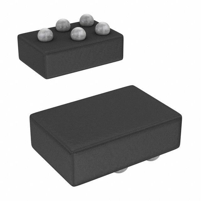
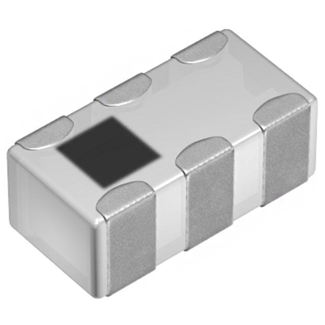
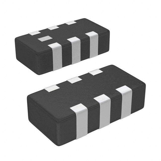
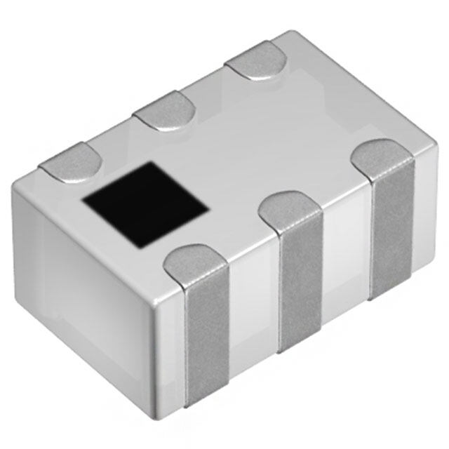
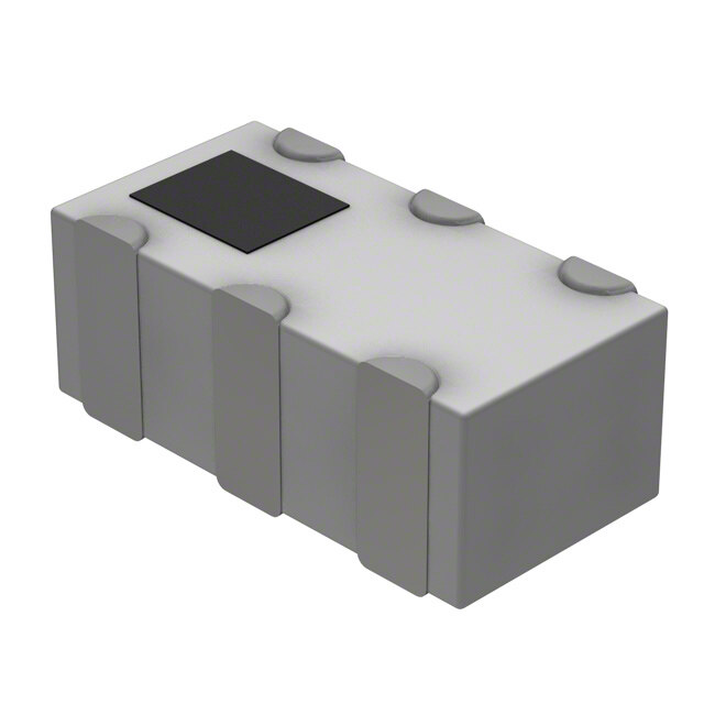
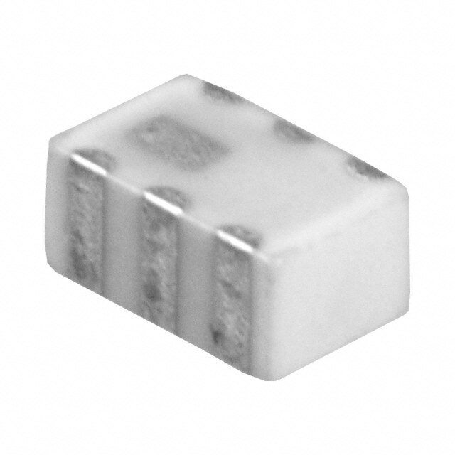
| 产品图片 |
|
| rohs | 符合RoHS无铅 / 符合限制有害物质指令(RoHS)规范要求 |
| 产品系列 | STMicroelectronics BAL-NRF01D3- |
| 数据手册 | |
| 产品型号 | BAL-NRF01D3 |
| 产品 | Baluns |
| 产品种类 | 信号调节 |
| 介入损耗 | 2.25 dB |
| 其它名称 | 497-13637-6 |
| 其它有关文件 | http://www.st.com/web/catalog/sense_power/FM139/CL1806/SC1508/PF253840?referrer=70071840 |
| 包装 | Digi-Reel® |
| 商标 | STMicroelectronics |
| 回波损耗(最小值) | 10dB |
| 安装类型 | 表面贴装 |
| 封装 | Reel |
| 封装/外壳 | 5-WFBGA,FCBGA |
| 封装/箱体 | FlipChip-5 |
| 工作温度范围 | - 40 C to + 85 C |
| 工厂包装数量 | 5000 |
| 插入损耗(最大值) | 2.25dB |
| 标准包装 | 1 |
| 相位差 | 3° |
| 端接类型 | SMD/SMT |
| 类型 | Ultraminiature Balun Integrated Matching Network and Harmonic Filter |
| 系列 | BAL-NRF01D3 |
| 阻抗 | 50 Ohms |
| 阻抗-非平衡/平衡 | 50 / - 欧姆 |
| 频率 | 2.4 GHz |
| 频率范围 | 2400 MHz to 2540 MHz |


- 商务部:美国ITC正式对集成电路等产品启动337调查
- 曝三星4nm工艺存在良率问题 高通将骁龙8 Gen1或转产台积电
- 太阳诱电将投资9.5亿元在常州建新厂生产MLCC 预计2023年完工
- 英特尔发布欧洲新工厂建设计划 深化IDM 2.0 战略
- 台积电先进制程称霸业界 有大客户加持明年业绩稳了
- 达到5530亿美元!SIA预计今年全球半导体销售额将创下新高
- 英特尔拟将自动驾驶子公司Mobileye上市 估值或超500亿美元
- 三星加码芯片和SET,合并消费电子和移动部门,撤换高东真等 CEO
- 三星电子宣布重大人事变动 还合并消费电子和移动部门
- 海关总署:前11个月进口集成电路产品价值2.52万亿元 增长14.8%

PDF Datasheet 数据手册内容提取
BAL-NRF01D3 50 Ω nominal input / conjugate match balun to nRF51422-QFAA, nRF24LE1, nRF51822-QFAA/AB, with integrated harmonic filter Datasheet - production data Description STMicroelectronics BAL-NRF01D3 is an ultraminiature balun. The device integrates matching network and harmonics filter. Matching impedance has been customized for the following Nordic Semiconductor circuits: nRF24LE1 QFN- 32 pins, nRF24AP2-1CH, nRF24AP2-8CH, nRF51422-QFAA (build code CA/C0), nRF51822-QFAA (build code CA/C0) and nRF51822-QFAB (build code AA/A0). Lead-freeFlip-Chip(5bumps)package The device uses STMicroelectronics’ IPD technology on a non-conductive glass substrate Features to optimize RF performance. 50 Ω nominal input / conjugate match to The BAL-NRF01D3 has been tested and Nordic Semiconductor chips nRF24LE1 approved by Nordic Semiconductor in their QFN32, nRF24AP2-1CH, nRF24AP2-8CH, nRF2723 and nRF2752 nRFgo modules. nRF51422-QFAA (build code CA/C0), Figure 1: Application schematic nRF51822-QFAA (build code CA/C0) and nRF51822-QFAB (build code AA/A0) 3 2 1 Low insertion loss Low amplitude imbalance Low phase imbalance A DIFF GND Small footprint < 1.5 mm2 B SE Benefits Very low profile < 595 μm after reflow DIFF VCC C High RF performance RF BOM and area reduction Applications 2.45 GHz impedance matched balun filter Optimized for Nordic's chip set nRF24LE1/AP2, nRF51422-QFAA (build code CA/C0), nRF51822-QFAA (build code CA/C0) and nRF51822-QFAB (build code AA/A0) June 2017 DocID023215 Rev 7 1/10 This is information on a product in full production. www.st.com
Characteristics BAL-NRF01D3 1 Characteristics Table 1: Absolute maximum ratings (limiting values) Value Symbol Parameter Unit Min. Typ. Max. PIN Input power RFIN - 20 dBm ESD ratings MIL STD883C 2000 - (HBM: C = 100 pF, R = 1.5 Ω, air discharge) ESD ratings charge device model VESD (JESD22-C101-C) 500 V ESD ratings machine model 200 - (MM: C = 200 pF, R = 25 W, L = 500 nH) TOP Operating temperature -40 - +105 °C Table 2: Impedances (T = 25 °C) amb Value Symbol Parameter Unit Min. Typ. Max. Conjugate match to: nRF24LE1/AP2 nRF51422-QFAA (build code Nominal differential output CA/C0) ZOUT impedance - nRF51822-QFAA (build code - Ω CA/C0) nRF51822-QFAB (build code AA/A0) ZIN Nominal input impedance - 50 - Ω Table 3: RF performance (Tamb = 25 °C) Value Symbol Parameter Test condition Unit Min. Typ. Max. F Frequency range (bandwidth) 2400 2540 2400 2540 MHz IL Insertion loss in bandwidth 2.25 dB RL Return loss in bandwidth 10 dB ɸimb Phase imbalance 3 ° Aimb Amplitude imbalance 0.1 dB 2f0 2nd harmonic filtering 4880 MHz 10 dB 3f0 3rd harmonic filtering 7320 MHz 20 dB 2/10 DocID023215 Rev 7
BAL-NRF01D3 Characteristics 1.1 RF measurement Figure 2: Transmission (Tamb = 25 °C) Figure 3: Return loss on SE port (Tamb = 25 °C) Figure 4: Return loss on DIFF port (Tamb = 25 °C) Figure 5: Amplitude imbalance (Tamb = 25 °C) Figure 6: Phase imbalance (Tamb = 25 °C) DocID023215 Rev 7 3/10
Application information BAL-NRF01D3 2 Application information Figure 7: Application schematic (courtesy of Nordic Semiconductor) BAL-NRF01D3 Figure 8: nRF2723 application board (courtesy of Nordic Semiconductor) 4/10 DocID023215 Rev 7
BAL-NRF01D3 Application information Figure 9: nRF2752 application board (courtesy of Nordic Semiconductor) BAL-NRF01D3 DocID023215 Rev 7 5/10
Package information BAL-NRF01D3 3 Package information In order to meet environmental requirements, ST offers these devices in different grades of ECOPACK® packages, depending on their level of environmental compliance. ECOPACK® specifications, grade definitions and product status are available at: www.st.com. ECOPACK® is an ST trademark. Epoxy meets UL94, V0 Lead-free package 3.1 Flip-Chip 5 bumps package information Figure 10: Flip-Chip 5 bumps package outline X T 1 B DIFF GND B D SE Y DIFF VCC 2 B 1 B A1 A A2 A1 T1 H Table 4: Flip-Chip 5 bumps dimensions Parameter Description Min. Typ. Max. Unit X X dimension of the die 1445 1485 1525 mm Y Y dimension of the die 980 1020 1060 mm A X pitch 604 mm B Y pitch 500 mm A1 Distance from bump to edge of die on X axis 224 mm B1 Distance from bump to edge of die on Y axis 260 mm A2 Distance from VCC bump to SE bump on X axis 433 mm B2 Distance from bump to edge of die on Y axis 510 mm C GND, VCC bump to SE bump pitch 500 mm D Bump diameter 240 255 260 mm T1 Substrate thickness 425 mm H Bump height 205 mm T Total die thickness 570 630 690 6/10 DocID023215 Rev 7
BAL-NRF01D3 Package information Figure 11: Footprint - 3 mils stencil -non solder Figure 12: Footprint - 3 mils stencil - solder mask mask defined defined Copperpaddiameter: Soldermaskopening: 220µmrecommended 220µmrecommended 180µmminimum 180µmminimum 260µmmaximum 260µmmaximum Soldermaskopening: Copperpaddiameter: 320µmrecommended 320µmrecommended 300µmminimum 300µmminimum 340µmmaximum Solderstencilopening: Solderstencilopening: 220µmrecommended 220µmrecommended Figure 13: Footprint - 5 mils stencil -non solder Figure 14: Footprint - 5 mils stencil - solder mask mask defined defined Copperpaddiameter: Soldermaskopening: 220µmrecommended 220µmrecommended 180µmminimum 180µmminimum 260µmmaximum 260µmmaximum Soldermaskopening: Copperpaddiameter: 320µmrecommended 320µmrecommended 300µmminimum 300µmminimum 340µmmaximum Solderstencilopening: Solderstencilopening: 330µmrecommended* 330µmrecommended* *dependingonpaste,itcangodownto270µm *dependingonpaste,itcangodownto270µm 3.2 Flip-chip 5 bumps packing information Figure 15: Marking Dot,STlogo ECOPACKgrade xx=marking x x z z=manufacturing location yww=datecode y w w DocID023215 Rev 7 7/10
Package information BAL-NRF01D3 Figure 16: Flip Chip tape and reel specifications More packing information is available in the application note: AN2348 Flip-Chip: “Package description and recommendations for use” AN4111: “BAL-NRF01D3 matched balun with integrated harmonics filter for Nordic Semiconductor chips with ultralow power transceivers” 8/10 DocID023215 Rev 7
BAL-NRF01D3 Ordering information 4 Ordering information Table 5: Ordering information Order code Marking Package Weight Base qty. Delivery mode BAL-NRF01D3 SC Flip-Chip package (5 bumps) 1.82 mg 5000 Tape and reel 5 Revision history Table 6: Document revision history Date Revision Changes 15-Oct-2012 1 First issue. Added references to nRF51 series. Added Figure 9. Updated y-axis 13-Nov-2012 2 labels in Figure 2. 04-Mar-2013 3 Updated footprint illustrations in Figure 13, and Figure 14. Added dimensions in Figure 10. Updated marking orientation in Figure 06-Aug-2013 4 11 and Figure 12. 13-Jan-2014 5 Updated document title and product references. 07-Jul-2015 6 Updated Table 1. Updated Figure 10: "Flip-Chip 5 bumps package outline" and Table 4: 21-Jun-2017 7 "Flip-Chip 5 bumps dimensions". DocID023215 Rev 7 9/10
BAL-NRF01D3 IMPORTANT NOTICE – PLEASE READ CAREFULLY STMicroelectronics NV and its subsidiaries (“ST”) reserve the right to make changes, corrections, enhancements, modifications, and improvements to ST products and/or to this document at any time without notice. Purchasers should obtain the latest relevant information on ST products before placing orders. ST products are sold pursuant to ST’s terms and conditions of sale in place at the time of order acknowledgement. Purchasers are solely responsible for the choice, selection, and use of ST products and ST assumes no liability for application assistance or the design of Purchasers’ products. No license, express or implied, to any intellectual property right is granted by ST herein. Resale of ST products with provisions different from the information set forth herein shall void any warranty granted by ST for such product. ST and the ST logo are trademarks of ST. All other product or service names are the property of their respective owners. Information in this document supersedes and replaces information previously supplied in any prior versions of this document. © 2017 STMicroelectronics – All rights reserved 10/10 DocID023215 Rev 7