ICGOO在线商城 > 集成电路(IC) > PMIC - 稳压器 - 线性 > BA05CC0FP-E2
 Datasheet下载
- 型号: BA05CC0FP-E2
- 制造商: ROHM Semiconductor
- 库位|库存: xxxx|xxxx
- 要求:
| 数量阶梯 | 香港交货 | 国内含税 |
| +xxxx | $xxxx | ¥xxxx |
查看当月历史价格
查看今年历史价格
BA05CC0FP-E2产品简介:
ICGOO电子元器件商城为您提供BA05CC0FP-E2由ROHM Semiconductor设计生产,在icgoo商城现货销售,并且可以通过原厂、代理商等渠道进行代购。 BA05CC0FP-E2价格参考¥8.31-¥8.31。ROHM SemiconductorBA05CC0FP-E2封装/规格:PMIC - 稳压器 - 线性, Linear Voltage Regulator IC Positive Fixed 1 Output 5V 1A TO-252-3。您可以下载BA05CC0FP-E2参考资料、Datasheet数据手册功能说明书,资料中有BA05CC0FP-E2 详细功能的应用电路图电压和使用方法及教程。
Rohm Semiconductor的BA05CC0FP-E2是一款线性电源管理IC(PMIC),主要用于低功耗和高精度的应用场景。以下是其主要应用场景:

 1. 便携式电子设备
   - 智能手机和平板电脑:该芯片具有低静态电流和高效率的特点,适合用于便携式设备中的电源管理,以延长电池寿命。
   - 可穿戴设备:如智能手表、健身追踪器等,需要高效且小型化的电源解决方案。

 2. 物联网(IoT)设备
   - BA05CC0FP-E2适用于低功耗传感器模块、无线通信模块(如蓝牙、Wi-Fi)以及边缘计算设备,确保在有限的电源条件下稳定运行。

 3. 医疗电子设备
   - 便携式医疗设备:如血糖仪、脉搏血氧仪等,这些设备要求高精度电压输出和低噪声特性,以保证测量结果的准确性。
   - 健康监测设备:如心率监测器和体温计,对电源的稳定性和可靠性要求较高。

 4. 工业控制与自动化
   - 在工业环境中,该芯片可用于为微控制器、传感器和其他低功耗组件供电,特别是在需要高稳定性和低噪声的应用中。

 5. 消费类电子产品
   - 音频设备:如耳机放大器、音响系统等,需要低噪声电源以减少音频失真。
   - 家用自动化设备:如智能插座、环境监测器等,对电源的效率和稳定性有较高要求。

 特点总结:
- 低功耗设计:适合电池供电的设备。
- 高精度电压调节:适用于对电压稳定性要求较高的场景。
- 小型化封装:便于集成到紧凑型设备中。
- 低噪声性能:确保敏感电路的正常工作。

因此,BA05CC0FP-E2广泛应用于需要高效、低功耗和高精度电源管理的各种领域。
| 参数 | 数值 |
| 产品目录 | 集成电路 (IC)半导体 |
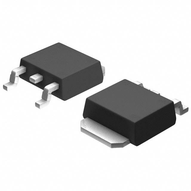
| 描述 | IC REG LDO 5V 1A TO252-3低压差稳压器 REG 1A 53V |
| 产品分类 | |
| 品牌 | ROHM Semiconductor |
| 产品手册 | |
| 产品图片 |
|
| rohs | 符合RoHS无铅 / 符合限制有害物质指令(RoHS)规范要求 |
| 产品系列 | 电源管理 IC,低压差稳压器,ROHM Semiconductor BA05CC0FP-E2- |
| 数据手册 | |
| 产品型号 | BA05CC0FP-E2 |
| 产品培训模块 | http://www.digikey.cn/PTM/IndividualPTM.page?site=cn&lang=zhs&ptm=30333 |
| 产品种类 | 低压差稳压器 |
| 供应商器件封装 | TO-252-3 |
| 其它名称 | BA05CC0FP-E2CT |
| 包装 | 剪切带 (CT) |
| 商标 | ROHM Semiconductor |
| 回动电压—最大值 | 500 mV at 500 mA |
| 安装类型 | 表面贴装 |
| 安装风格 | SMD/SMT |
| 封装 | Reel |
| 封装/外壳 | TO-252-3,DPak(2 引线+接片),SC-63 |
| 封装/箱体 | TO-252-3 |
| 工作温度 | -40°C ~ 125°C |
| 工厂包装数量 | 2000 |
| 最大功率耗散 | 1.2 W |
| 最大工作温度 | + 125 C |
| 最大输入电压 | 25 V |
| 最小工作温度 | - 40 C |
| 最小输入电压 | 4 V |
| 标准包装 | 1 |
| 特色产品 | http://www.digikey.cn/product-highlights/cn/zh/rohm-ba-bd-ldo-regulator-ics/3995 |
| 电压-跌落(典型值) | 0.3V @ 500mA |
| 电压-输入 | 最高 25V |
| 电压-输出 | 5V |
| 电压调节准确度 | 2 % |
| 电流-输出 | 1A |
| 电流-限制(最小值) | - |
| 稳压器拓扑 | 正,固定式 |
| 稳压器数 | 1 |
| 线路调整率 | 100 mV |
| 负载调节 | 150 mV |
| 输出电压 | 5 V |
| 输出电流 | 1 A |
| 输出端数量 | 1 Output |
| 输出类型 | Fixed |


- 商务部:美国ITC正式对集成电路等产品启动337调查
- 曝三星4nm工艺存在良率问题 高通将骁龙8 Gen1或转产台积电
- 太阳诱电将投资9.5亿元在常州建新厂生产MLCC 预计2023年完工
- 英特尔发布欧洲新工厂建设计划 深化IDM 2.0 战略
- 台积电先进制程称霸业界 有大客户加持明年业绩稳了
- 达到5530亿美元!SIA预计今年全球半导体销售额将创下新高
- 英特尔拟将自动驾驶子公司Mobileye上市 估值或超500亿美元
- 三星加码芯片和SET,合并消费电子和移动部门,撤换高东真等 CEO
- 三星电子宣布重大人事变动 还合并消费电子和移动部门
- 海关总署:前11个月进口集成电路产品价值2.52万亿元 增长14.8%


PDF Datasheet 数据手册内容提取
Datasheet 2A/1A Fixed Output LDO Regulators BAxxDD0T Series BAxxCC0T Series BAxxCC0FP Series 2A/1A Fixed Output LDO Regulators With Shutdown Swicth BAxxDD0WT Series BAxxDD0HFP Series BAxxCC0WT Series BAxxCC0W FP Series ●General Description Standard Fixed Output LDO Regulators are low-saturation regulators, available for output s up to 2A / 1A. ROHM has a wide output voltage range and package lineup with and without shutdown switches. This IC has a built-in over-current protection circuit that prevents the destruction of the IC due to output short circuits, a thermal shut-down circuit that protects the IC from damage due to overloading and an over-voltage protection circuit that protects the IC from surges generated in the power supply line of the IC. ●Features ●Packages W (Typ.) x D (Typ.) x H (Max.) (cid:132) ±1% highly accurate output voltage (BAxxDD0xx) HRP5 9.395mm x 10.54mm x 2.005mm (cid:132) Low saturation with PNP output TO252-3 6.50 mm x 9.50mm x 2.50 mm (cid:132) Built-in over-current protection circuit that prevents TO252-5 6.50 mm x 9.50mm x 2.50 mm the destruction of the IC due to output short circuits TO220FP-3 10.00 mm x 30.50mm x 4.60 mm (cid:132) Built-in thermal shutdown circuit for protecting the IC TO220FP-5 10.00 mm x 30.50mm x 4.60 mm from damage due to overloading (cid:132) Built-in over- voltage protection circuit that prevents the destruction of the IC due to power supply surges ●Key Specification (cid:132) Input Power Supply Voltage: 25V (Max.) (cid:132) Output voltage type: Fixed HRP5 TO252-3 TO252-5 (cid:132) Output current: BAxxDD0xx series 2A (Max.) BAxxCC0xx series 1A (Max.) (cid:132) Shutdown current: 0μA(Typ.) (cid:132) Operating temperature range: -40℃ to +125℃ ●Applications Used in DSP power supplies for DVD and CD players, FPDs, televisions, personal computers or any other consumer device ●Lineup matrix TO220FP-3 TO220FP-5 ■1A output BAxxCC0xx Series Output voltage (V) Part Number Package 3.0 3.3 5.0 6.0 7.0 8.0 9.0 10.0 12.0 15.0 BAxxCC0WT ○ ○ ○ - ○ ○ ○ ○ ○ - TO220FP-5 BAxxCC0WFP - ○ ○ ○ ○ ○ ○ - ○ - TO252-5 BAxxCC0T ○ ○ ○ ○ ○ ○ ○ ○ ○ ○ TO220FP-3 BAxxCC0FP ○ ○ ○ ○ ○ ○ ○ ○ ○ ○ TO252-3 ■2A output BAxxDD0xx Series Output voltage (V) Part Number Package 1.5 1.8 2.5 3.0 3.3 5.0 9.0 12.0 16.0 BAxxDD0WT ○ ○ ○ ○ ○ ○ ○ ○ ○ TO220FP-5 BAxxDD0WHFP ○ ○ ○ ○ ○ ○ ○ ○ ○ HRP5 BAxxDD0T ○ ○ ○ ○ ○ ○ ○ ○ ○ TO220FP-3 ○Product structure : Silicon monolithic integrated circuit ○This product is not designed protection against radioactive rays. www.rohm.com TSZ02201-0R6R0A600130-1-2 © 2013 ROHM Co., Ltd. All rights reserved. 1/20 TSZ22111・14・001 9.Aug.2013 Rev.003
BAxxDD0xx BAxxCC0xx Datasheet ●Ordering Information B A x x x x 0 x x x x - x x Part Output voltage Output Shutdown Switch Package Packaging and forming specification Number Current W : Includes switch HFP : HRP5 TR: Embossed tape and reel (HRP5) CC0 : 1A None: without switch FP : TO252-5 E2: Embossed tape and reel DD0 : 2A : TO252-3 (TO252-3,TO252-5) None : Container Tube T : TO220FP-5 (TO220FP-3,TO220FP-5) : TO220FP-3 ●Lineup ■1A output BAxxCC0xx Series Maximum output Shutdown Output Orderable Package current (Max.) Switch voltage(Typ.) Part Number 3.3V BA033CC0WFP-E2 5.0V BA05CC0WFP-E2 6.0V BA06CC0WFP-E2 TO252-5 Reel of 2000 7.0V BA07CC0WFP-E2 8.0V BA08CC0WFP-E2 9.0V BA09CC0WFP-E2 12.0V BAJ2CC0WFP-E2 With Switch 3.0V BA03CC0WT 3.3V BA033CC0WT 5.0V BA05CC0WT 7.0V BA07CC0WT TO220FP-5 Tube of 500 8.0V BA08CC0WT 9.0V BA09CC0WT 10.0V BAJ0CC0WT 12.0V BAJ2CC0WT 3.0V BA03CC0FP-E2 3.3V BA033CC0FP-E2 1A 5.0V BA05CC0FP-E2 6.0V BA06CC0FP-E2 7.0V BA07CC0FP-E2 TO252-3 Reel of 2000 8.0V BA08CC0FP-E2 9.0V BA09CC0FP-E2 10.0V BAJ0CC0FP-E2 12.0V BAJ2CC0FP-E2 15.0V BAJ5CC0FP-E2 No switch 3.0V BA03CC0T 3.3V BA033CC0T 5.0V BA05CC0T 6.0V BA06CC0T 7.0V BA07CC0T TO220FP-3 Tube of 500 8.0V BA08CC0T 9.0V BA09CC0T 10.0V BAJ0CC0T 12.0V BAJ2CC0T 15.0V BAJ5CC0T www.rohm.com TSZ02201-0R6R0A600130-1-2 © 2013 ROHM Co., Ltd. All rights reserved. 2/20 TSZ22111・15・001 9.Aug.2013 Rev.003
BAxxDD0xx BAxxCC0xx Datasheet ■2A output BAxxDD0xx Series Maximum output Shutdown Output Orderable Package current (Max.) Switch voltage(Typ.) Part Number 1.5V BA15DD0WT 1.8V BA18DD0WT 2.5V BA25DD0WT 3.0V BA30DD0WT TO220FP-5 Tube of 500 3.3V BA33DD0WT 5.0V BA50DD0WT 9.0V BA90DD0WT 12.0V BAJ2DD0WT 16.0V BAJ6DD0WT With Switch 1.5V BA15DD0WHFP-TR 1.8V BA18DD0WHFP-TR 2.5V BA25DD0WHFP-TR 3.0V BA30DD0WHFP-TR 2A HRP5 Reel of 2000 3.3V BA33DD0WHFP-TR 5.0V BA50DD0WHFP-TR 9.0V BA90DD0WHFP-TR 12.0V BAJ2DD0WHFP-TR 16.0V BAJ6DD0WHFP-TR 1.5V BA15DD0T 1.8V BA18DD0T 2.5V BA25DD0T 3.0V BA30DD0T No switch TO220FP-3 Tube of 500 3.3V BA33DD0T 5.0V BA50DD0T 9.0V BA90DD0T 12.0V BAJ2DD0T 16.0V BAJ6DD0T www.rohm.com TSZ02201-0R6R0A600130-1-2 © 2013 ROHM Co., Ltd. All rights reserved. 3/20 TSZ22111・15・001 9.Aug.2013 Rev.003
BAxxDD0xx BAxxCC0xx Datasheet ●Block Diagrams / Pin Configurations / Pin Descriptions BAxxCC0WFP/ BAxxDD0WHFP/ BAxxCC0WT/ BAxxDD0WT GND(TO252-5・HRP5) Fin Vcc Vref Driver R2 R1 OVP TSD OCP 1 2 3 4 5 CTL Vcc N.C. OUT N.C. (TO252-5) GND (TO220FP-5,HRP5) Fig.1 TOP VIEW PIN No. Pin Name Function 1 CTL Output voltage ON/OFF control FIN 2 Vcc Power supply voltage input 3 N.C./GND Unconnected terminal/GND*1 4 OUT Voltage output 1 2 3 4 5 1 2 3 4 5 TO252-5 HRP5 5 N.C. Unconnected terminal 1 2 3 4 5 Fin GND GND*2 TO220FP-5 1 * TO252-5=N.C.,TO220FP-5,HRP5=GND *2 TO252-5,HRP5 only BAxxCC0T/ BAxxCC0FP/ BAxxDD0T Fin GND(TO252-3) Vcc Vref Driver R2 OV P TSD OCP R1 1 2 3 Vcc N.C. OUT (TO252-3) GND (TO220FP-3) Fig.2 TOP VIEW PIN No. Pin Name Function 1 Vcc Power supply voltage input FIN 2 N.C./GND Unconnected terminal/GND*1 3 OUT Voltage output Fi GND GND*2 2 1 3 TO252-3 *1 TO252-3=N.C.,TO220FP-3=GND 1 2 3 2 TO220FP-3 * TO252-3 only www.rohm.com TSZ02201-0R6R0A600130-1-2 © 2013 ROHM Co., Ltd. All rights reserved. 4/20 TSZ22111・15・001 9.Aug.2013 Rev.003
BAxxDD0xx BAxxCC0xx Datasheet ●Absolute Maximum Ratings (Ta=25℃) Parameter Symbol Ratings Unit Input Power Supply Voltage*1 V -0.3 to +35 V CC 2300(HRP5) 1300(TO252-5) Power Dissipation*2 Pd mW 1200(TO252-3) 2000(TO220FP-3,5) Operating Temperature Range Topr -40 to +125 ℃ Ambient Storage Temperature Tstg -55 to +150 ℃ Junction Temperature Tj +150 ℃ MAX. Output Control Terminal Voltage*3 Vctl -0.3 to +Vcc V Voltage Applied to the Tip *4 VCC peak +50 V *1 Must not exceed Pd tr≧1msec *2 HRP5 : In cases in which Ta≧25℃ when a 70mm×70mm×1.6mm glass epoxy board is used, the power is reduced by 18.4 mW/℃. TO252FP-3 : In cases in which Ta≧25℃ when a 70mm×70mm×1.6mm glass 50V epoxy board is used, the power is reduced by 9.6 mW/℃. TO252FP-5 : In cases in which Ta≧25℃ when a 70mm×70mm×1.6mm glass 35V epoxy board is used, the power is reduced by 10.4 mW/℃. TO220FP-5 : No heat sink. When Ta≧25℃, the power is reduced by 16 mW/℃. MAX200msec *3 Only for models with shutdown switches. 0V (Voltage Supply more than 35V) *4 Applied voltage : 200msec or less (tr≥1msec) ●Recommended Operating Ratings (Ta=25℃) Ratings Parameter Symbol Unit Min. Typ. Max. Input BAxxCC0xx 4.0 ― 25.0 V Power Supply V CC Voltage BAxxDD0xx 3.0 ― 25.0 V BAxxCC0xx ― ― 1 A Output Current Io BAxxDD0xx ― ― 2 A Output Control Terminal Voltage Vctl 0 ― V V CC www.rohm.com TSZ02201-0R6R0A600130-1-2 © 2013 ROHM Co., Ltd. All rights reserved. 5/20 TSZ22111・15・001 9.Aug.2013 Rev.003
BAxxDD0xx BAxxCC0xx Datasheet ●Electrical Characteristics BAxxCC0 Series (Unless otherwise specified, Ta=25℃, VCTL=5V, Io=500mA Setting *5) Limit Parameter Symbol Unit Conditions Min. Typ. Max. Vo(T)× Vo(T)× Output Voltage *6 Vo Vo(T) V 0.98 1.02 Shut Down Current Isd - 0 10 μA VCTL=0V Bias Current Ib - 2.5 5.0 mA VCTL=2V, Io=0mA Dropout Voltage ΔVd - 0.3 0.5 V Vcc=Vo×0.95 Peak Output Current Io 1.0 - - A f=120Hz, ein*7=1Vrms, Ripple Rejection R.R. 45 55 - dB Io=100mA Line Regulation Reg.I - 20 100 mV Vcc=Vo(T)+1→25V Load Regulation Reg.L - 50 150 mV Io=5mA→1A Temperature Coefficient of Tcvo - ±0.02 - %/℃ Io=5mA,Tj=0 to 125℃ Output Voltage *8 Output Short Current Ios - 0.40 - A Vcc=25V ON Mode Voltage VthH 2.0 - - V ACTIVE MODE, Io=0mA OFF Mode Voltage VthL - - 0.8 V OFF MODE, Io=0mA Input High Current ICTL 100 200 300 μA VCTL=5V, Io=0mA BAxxDD0 series (Unless otherwise specified, Ta=25℃, VCTL=3V, Vcc=VCCT*9) Limit Parameter Symbol Unit Conditions Min. Typ. Max. Shut Down Current Isd - 0 10 μA VCTL=0V, Io=0mA Bias Current Ib - 0.9 2.0 mA Io=0mA Votyp× Votyp× Output Voltage *10 Vo Votyp V Io=200mA 0.99 1.01 Dropout Voltage 1 *11 ΔVd1 - 0.3 0.5 V Vcc=0.95×Vo, Io=1A Dropout Voltage 2 *11 ΔVd2 - 0.45 0.7 V Vcc=0.95×Vo, Io=2A Peak Output Current Io 2.0 - - A Ripple Rejection R.R. - 55 - dB f=120Hz, ein*7=-20dBV, Io=100mA Line Regulation Reg.I - 15 50 mV Vcc=VCCT*9V→25V, Io=200mA Load Regulation Reg.L - 50 200 mV Io=0mA→2A Temperature Coefficient of Output Voltage *8 Tcvo - ±0.02 - %/℃ Io=5mA, Tj=0 to 125℃ CTL ON Mode Voltage Von 2.0 - Vcc V ACTIVE MODE, Io=0mA CTL OFF Mode Voltage Voff - - 0.8 V OFF MODE, Io=0mA CTL Input Current ICTL - 60 120 μA VCTL=3V, Io=0mA *5 Vo=3.0V:Vcc=8.0V, 3.3V:Vcc=8.3V, Vo=5V:Vcc=10V, Vo=6V:Vcc=11V, Vo=7V:Vcc=12V, Vo=8V:Vcc=13V, Vo=9V:Vcc=14V, Vo=12V:Vcc=17V, Vo=15V:Vcc=20V *6 Vo(T)=3.0, 3.3, 5.0, 6.0, 7.0, 8.0, 9.0,12, 15V *7 ein : Input Voltage Ripple *8 Not 100% tested *9 Vo=1.5V,1.8V,2.5V,3.0V:VCCT =4.0V、Vo=3.3V,5.0V:VCCT =7.0V、Vo=9V:VCCT =12.0V、Vo=12V:VCCT =14.0V、Vo=16V:VCCT =18.0V) *10 Votyp=1.5V,1.8V,2.5V,3.0V,3.3V,5.0V,9.0V,12.0V,16.0V *11 Vo≧3.0V www.rohm.com TSZ02201-0R6R0A600130-1-2 © 2013 ROHM Co., Ltd. All rights reserved. 6/20 TSZ22111・15・001 9.Aug.2013 Rev.003
BAxxDD0xx BAxxCC0xx Datasheet ●Typical Performance Curves (Unless specified otherwise, Vcc=8.3V, Vo=3.3V, V =5.0V, and Io=0mA) CTL BAxxCC0xx (BA33CC0WT) Fig.3 Fig.4 Circuit current Input Stability Fig.5 Fig.6 Input Stability Load Stability (Io=500mA) www.rohm.com TSZ02201-0R6R0A600130-1-2 © 2013 ROHM Co., Ltd. All rights reserved. 7/20 TSZ22111・15・001 9.Aug.2013 Rev.003
BAxxDD0xx BAxxCC0xx Datasheet ●Typical Performance Curves - continued Fig.7 Fig.8 Input/Output Voltage Difference Ripple Rejection Characteristics Io-△Vd Characteristics (Vcc=2.95V) (Io=100mA) Fig.10 Fig.9 Circuit Current by load Level Output Voltage Temperature Characteristics (IOUT=0mA→1A) www.rohm.com TSZ02201-0R6R0A600130-1-2 © 2013 ROHM Co., Ltd. All rights reserved. 8/20 TSZ22111・15・001 9.Aug.2013 Rev.003
BAxxDD0xx BAxxCC0xx Datasheet ●Typical Performance Curves - continued Fig.12 Fig.11 CTL Voltage vs. Output Voltage CTL Voltage vs. CTL Current Fig.13 Fig.14 Overvoltage Operating Thermal Shutdown Characteristics (Io=200mA) Circuit Characteristics www.rohm.com TSZ02201-0R6R0A600130-1-2 © 2013 ROHM Co., Ltd. All rights reserved. 9/20 TSZ22111・15・001 9.Aug.2013 Rev.003
BAxxDD0xx BAxxCC0xx Datasheet ●Typical Performance Curves - continued (Unless specified otherwise, Vcc=7.0V, Vo=5.0V, VCTL=3.0V, and Io=0mA) BAxxDD0xx (BA50DD0WT) Fig.15 Fig.16 Circuit Current Input Stability (Io=0mA) Fig.18 Fig.17 Load Stability Input Stability (Io=2A) www.rohm.com TSZ02201-0R6R0A600130-1-2 © 2013 ROHM Co., Ltd. All rights reserved. 10/20 TSZ22111・15・001 9.Aug.2013 Rev.003
BAxxDD0xx BAxxCC0xx Datasheet ●Typical Performance Curves - continued Fig.19 Fig.20 Input/Output Voltage Difference Ripple Rejection Characteristics Fig.21 Fig.22 Temperature Characteristics Circuit Current by Load Level (lout=0mA→2A) www.rohm.com TSZ02201-0R6R0A600130-1-2 © 2013 ROHM Co., Ltd. All rights reserved. 11/20 TSZ22111・15・001 9.Aug.2013 Rev.003
BAxxDD0xx BAxxCC0xx Datasheet ●Typical Performance Curves - continued [BA50DD0WT] V] [ Fig.24 Fig.23 CTL Voltage vs. Output Voltage CTL Voltage vs. CTL Current Fig.25 Fig.26 Overvoltage Operating Thermal Shutdown (lo=200mA) Circuit Characteristics www.rohm.com TSZ02201-0R6R0A600130-1-2 © 2013 ROHM Co., Ltd. All rights reserved. 12/20 TSZ22111・15・001 9.Aug.2013 Rev.003
BAxxDD0xx BAxxCC0xx Datasheet ●I/O equivalence circuit <BAxxDD0xx Series> <BAxxCC0xx Series> VVcccc Vcc 10kΩ Vcc OUT 25kΩ 39kΩ 2kΩ R 2 CTL 25kΩ 10kΩ OUT CTL R2 31kΩ R1 R1 Fig.27 Fig.28 ●Power Dissipation HRP-5 TO220FP-5 10 25 Board size : 70×70×1.6㎜3 (board contains a thermal via) When using a maximum heat sick : θj-c=6.25(℃/W) 9 Board front copper foil area : 10.5×10.5㎜2 When using an IC alone : θj-6=62.5(℃/W) ①2-layer board (back surface copper foil area :15×15㎜2) 8 ②③24--llaayyeerr bbooaarrdd ((bbaacckk ssuurrffaaccee ccooppppeerr ffooiill aarreeaa ::7700××7700㎜㎜22)) 20 (1)20.0 W)7 ③7.3W d(W) wer Dissipation:Pd(456 ②5.5W Power Dissipation:P1105 Po3 2 5 ①2.3W (2)2.0 1 0 0 0 25 50 75 100 125 150 0 25 50 75 100 125 150 Ambient temperature:Ta(℃) Ambient temperature:Ta(℃) Fig.30 Fig.29 TO252-5 2.0 Mounted on a Rohm standard board Board size : 70×70×1.6㎜ Copper foil area :7×7㎜ 1.6 TO252-5θja=96.2(℃/W) W) 1.30 d( on:P1.2 pati ssi er Di0.8 w o P 0.4 0.0 0 25 50 75 100 125 150 Ambient temperature:Ta(℃) Fig.31 www.rohm.com TSZ02201-0R6R0A600130-1-2 © 2013 ROHM Co., Ltd. All rights reserved. 13/20 TSZ22111・15・001 9.Aug.2013 Rev.003
BAxxDD0xx BAxxCC0xx Datasheet When using at temperatures over Ta=25℃, please refer to the heat reducing characteristics shown in Fig.29 through 31. The IC characteristics are closely related to the temperature at which the IC is used and if the temperature exceeds the maximum junction temperature TjMAX., the elements may be damaged or destroyed. From the standpoints of instantaneous destruction and long-term operating reliability, it is necessary give sufficient consideration to IC heat. In order to protect the IC from thermal damage, it is necessary to operate it at temperatures lower than the maximum junction temperature TjMAX of the IC. Fig.30 shows the acceptable loss and heat reducing characteristics of the TO220FP package The portion shown by the diagonal line is the acceptable loss range that can be used with the IC alone. Even when the ambient temperature Ta is a normal temperature (25℃), the chip (junction) temperature Tj may be quite high so please operate the IC at temperatures less than the acceptable loss Pd. The method of calculating the power consumption Pc (W) is as follows. Vcc:Input voltage Vo:Output voltage Io:Load current Pc = (Vcc-Vo) × Io + Vcc × Icca Vcca:Circuit current Acceptable loss Pd≦Pc Solving this for load current I in order to operate within the acceptable loss: O Pd – Vcc×Icca Io ≦ Vcc-Vo (Please refer to Fig.10 and 22 for Icca.) It is then possible to find the maximum load current IoMAX with respect to the applied voltage Vcc at the time of thermal design. ・Calculation Example Example 1) When Ta=85℃, Vcc=8.3V, Vo=3.3V, BA33DD0WT 1.04-8.3×Icca Io≦ With the IC alone : θja=62.5℃/W → -16mW/℃ 5 Io≦200mA (Icca : 2mA) 25℃=2000mW → 85℃=1040mW Please refer to the above information and keep thermal designs within the scope of acceptable loss for all operating temperature ranges. The power consumption Pc of the IC when there is a short circuit (short between Vo and GND) is: Pc=Vcc×(Icca+Ishort) *Ishort: Short circuit current ●Peripheral Circuit Considerations ・Vcc Terminal Please attach a capacitor (greater than 0.33µF) between the Vcc and GND. The capacitance values will differ depending on the application, so please take this into account when configuring the terminal. ・GND Terminal Please be sure to keep the set ground and IC ground at the same potential level so that a potential difference does not arise between them. If a potential difference arises between the set ground and the IC ground, the preset voltage will not be outputted, causing the system to become unstable. Therefore, please reduce the impedance by making the ground patterns as wide as possible and by reducing the distance between the set ground and the IC ground as much as possible. ・CTL Terminal The CTL terminal is turned ON at 2.0V and higher and OFF at 0.8V and lower within the operating power supply voltage range. CC0xx series, the power supply and the CTL terminal in any order without problems. ●Vo Terminal 100 100 Ω] Unstable operating region Ω] Unstable operating region IC OUT 22μF EFFECTIVE SERIES RESISTANCE:ESR [ 1010.1 SUtanbstlea bolep eorpa etirnagt inregg rieongi on EFFECTIVE SERIES RESISTANCE:ESR [ 011.01 UnSstatabblele o oppeerar atitningg r ereggioionn 0 20O0 UTPU4T0 0CURRE60N0T:lo(m8A00) 1000 11 10 OUTPUT CUR1R0E0 NT:lo(mA) 1000 10000 Fig.32 Output Equivalent Circuit Fig.33 ESR-Io Characteristics Fig.34 ESR vs. Io Characteristics (BAxxCC0) (BAxxDD0) Please attach an anti-oscillation capacitor between Vo and GND. The capacitance of the capacitor may significantly change due to factors such as temperature changes, making it impossible to completely stop oscillations. Please use a tantalum capacitor or aluminum electrolysis capacitor with favorable characteristics and small internal series resistance (ESR) even at low temperatures. The output fluctuates regardless of whether the ESR is large or small. Please use the IC within the stable operating region while referring to the ESR characteristics reference data shown in Fig.32 through 34. In applications where there are sudden load fluctuations, the use of a capacitor with large capacitance is recommended. www.rohm.com TSZ02201-0R6R0A600130-1-2 © 2013 ROHM Co., Ltd. All rights reserved. 14/20 TSZ22111・15・001 9.Aug.2013 Rev.003
BAxxDD0xx BAxxCC0xx Datasheet ●Operational Notes 1) Protection Circuits Over-current Protection Circuit A built-in over-current protection circuit corresponding to the current capacity prevents the destruction of the IC when there are load shorts. This protection circuit is a “7”-shaped current control circuit that is designed such that the current is restricted and does not latch even when a large current momentarily flows through the system with a high-capacitance capacitor. However, while this protection circuit is effective for the prevention of destruction due to unexpected accidents, it is not suitable for continuous operation or transient use. Please be aware when creating thermal designs that the overcurrent protection circuit has negative current capacity characteristics with regard to temperature (Refer to Fig.6 and 18). Thermal Shutdown Circuit (Thermal Protection) This system has a built-in temperature protection circuit for the purpose of protecting the IC from thermal damage. As shown above, this must be used within the range of acceptable loss, but if the acceptable loss happens to be continuously exceeded, the chip temperature Tj increases, causing the temperature protection circuit to operate. When the thermal shutdown circuit operates, the operation of the circuit is suspended. The circuit resumes operation immediately after the chip temperature Tj decreases, so the output repeats the ON and OFF states (Please refer to Fig.14 and 26 for the temperatures at which the temperature protection circuit operates). There are cases in which the IC is destroyed due to thermal runaway when it is left in the overloaded state. Be sure to avoid leaving the IC in the overloaded state. Reverse Current In order to prevent the destruction of the IC when a reverse current flows through the IC, it is recommended that a diode be placed between the Vcc and Vo and a pathway be created so that the current can escape (Refer to Fig.35). Reverse current Vcc OUT CTL GND Fig.35 Bypass diode 2) This IC is bipolar IC that has a P-board (substrate) and P+ isolation layer between each devise, as shown in Fig.36. A P-N junction is formed between this P-layer and the N-layer of each device, and the P-N junction operates as a parasitic diode when the electric potential relationship is GND> Pin A, GND> Pin B, while it operates as a parasitic transistor when the electric potential relationship is Pin B GND> Pin A. Parasitic devices are structurally inevitable in the IC. The operation of parasitic devices induces mutual interference between circuits, causing malfunctions and eventually the destruction of the IC. It is necessary to be careful not to use the IC in ways that would cause parasitic elements to operate. For example, applying a voltage that is lower than the GND (P-board) to the input terminal. Transistor (NPN) Resistor (Pin B) (Pin B) (Pin A) C B E C B GND E N P+ N P P+ N P+ NN P P+ N GNDPo ra trraasnitsicis teoler ment N P P a ra s it ic e lement P (Pin A) GND GND Parasitic element Parasitic element or transistor GND Fig.36 Example of the basic structure of a bipolar IC Status of this document The Japanese version of this document is formal specification. A customer may use this translation version only for a reference to help reading the formal version. If there are any differences in translation version of this document formal version takes priority. www.rohm.com TSZ02201-0R6R0A600130-1-2 © 2013 ROHM Co., Ltd. All rights reserved. 15/20 TSZ22111・15・001 9.Aug.2013 Rev.003
BAxxDD0xx BAxxCC0xx Datasheet ●Physical Dimension Tape and Reel Information HRP5 <Tape and Reel information> 9.395±0.125 (MAX 9.745 include BURR) Tape Embossed carrier tape ±1.0170.2 8.(862.5 ±) 0.1 1.905±0.1 Quantity 2T0R00pcs Direction ±8.00.13 (7.49) ±2.0538.0±1.5230.15±10.540.13 of feed (Treheel odnir ethcetio lenf tis h tahned 1 apnind oyfo pur opduull cot uist taht1e t phtaienp uep opne rt hrieg hritg whth heann ydou hold ) 1.2575 1 2 3 4 5 4.5°−++450...551°° 0.27−0.05 ±0.080.05 1.72 0.008.73S±0.1 S (Unit : mm) Reel ∗ Order quantity needs to be multipDlei roef cthtieo nm ionfim feuemd quantity. TO252-3 <Tape and Reel information> 6.5±0.2 Tape Embossed carrier tape ±1.50.2 5.F1I-+N00..12 C0.5 2.3±0.2 0.5±0.1 QDofiu rfeaecnettdiiotyn 2E(02T0h0ep dcisrection is the 1pin of product is at the lower left when you hold ) reel on the left hand and you pull out the tape on the right hand ±5.50.2 ±9.50.5 1 0.8 2 3 1.5 2.5 0.65 0.65 0.5±0.1 0.75 2.3±0.2 2.3±0.2 1.0±0.2 1pin Direction of feed (Unit : mm) Reel ∗ Order quantity needs to be multiple of the minimum quantity. TO252-5 <Tape and Reel information> 6.5±0.2 2.3±0.2 Tape Embossed carrier tape Quantity 2000pcs ±1.50.2 5.1+-00..12 C0.5 0.5±0.1 Dofi rfeecetdion E(2The direction is the 1pin of product is at the lower left when you hold ) reel on the left hand and you pull out the tape on the right hand FIN ±5.50.2 ±9.50.5 1230.8 4 5 1.5 2.5 0.5±0.1 0.5 1.27 1.0±0.2 1pin Direction of feed (Unit : mm) Reel ∗ Order quantity needs to be multiple of the minimum quantity. TO220FP-3 <Tape and Reel information> 10.0+−00..31 4.5+−00..31 ±1.80.2 7.0+−00..31 φ3.2±0.1 2.8+−00..21 CQounatnatiintyer T50u0bpecs Direction of feed Direction of products is fixed in a container tube +0.417.0−0.2 ±12.00.2 ±8.00.2 13.5Min. ±5.00.2 01..83 2.54±0.5 2.54±0.5 0.55 +−00..105 2.6±0.5 1 2 3 (Unit : mm) ∗ Order quantity needs to be multiple of the minimum quantity. www.rohm.com TSZ02201-0R6R0A600130-1-2 © 2013 ROHM Co., Ltd. All rights reserved. 16/20 TSZ22111・15・001 9.Aug.2013 Rev.003
BAxxDD0xx BAxxCC0xx Datasheet TO220FP-5 <Tape and Reel information> 10.0+−00..31 4.5+−00..31 Container Tube ±1.80.2 7.0+−00..31 φ3.2±0.1 2.8+−00..21 Quantity 500pcs Direction of feed Direction of products is fixed in a container tube +0.417.0−0.2 ±12.00.2 ±8.00.20.7 Min. 1.2 13.5 0.8 1.778 0.5±0.1 2.85 12345 (Unit : mm) ∗ Order quantity needs to be multiple of the minimum quantity. ●Marking Diagrams HRP5 ( TOP VIE W) Part Number Marking LOT Number 1PIN MARK TO252-3 TO252-5 (TOP VIEW) (TOP VIEW) Part Number Marking Part Number Marking LOT Number LOT Number TO220FP-3 (TOP VIEW) TO220FP-5 (TOP VIEW) Part Number Marking Part Number Marking LOT Number LOT Number www.rohm.com TSZ02201-0R6R0A600130-1-2 © 2013 ROHM Co., Ltd. All rights reserved. 17/20 TSZ22111・15・001 9.Aug.2013 Rev.003
BAxxDD0xx BAxxCC0xx Datasheet ■1A output BAxxCC0xx Series Orderable Part Number Package Part Number Marking BA033CC0WFP-E2 033CC0W BA05CC0WFP-E2 05CC0W BA06CC0WFP-E2 06CC0W BA07CC0WFP-E2 TO252-5 07CC0W BA08CC0WFP-E2 08CC0W BA09CC0WFP-E2 09CC0W BAJ2CC0WFP-E2 J2CC0W BA03CC0WT 03CC0W BA033CC0WT 033CC0W BA05CC0WT 05CC0W BA07CC0WT 07CC0W TO220FP-5 BA08CC0WT 08CC0W BA09CC0WT 09CC0W BAJ0CC0WT J0CC0W BAJ2CC0WT J2CC0W BA03CC0FP-E2 03CC0 BA033CC0FP-E2 033CC0 BA05CC0FP-E2 05CC0 BA06CC0FP-E2 06CC0 BA07CC0FP-E2 07CC0 TO252-3 BA08CC0FP-E2 08CC0 BA09CC0FP-E2 09CC0 BAJ0CC0FP-E2 J0CC0 BAJ2CC0FP-E2 J2CC0 BAJ5CC0FP-E2 J5CC0 BA03CC0T 03CC0 BA033CC0T 033CC0 BA05CC0T 05CC0 BA06CC0T 06CC0 BA07CC0T 07CC0 TO220FP-3 BA08CC0T 08CC0 BA09CC0T 09CC0 BAJ0CC0T J0CC0 BAJ2CC0T J2CC0 BAJ5CC0T J5CC0 www.rohm.com TSZ02201-0R6R0A600130-1-2 © 2013 ROHM Co., Ltd. All rights reserved. 18/20 TSZ22111・15・001 9.Aug.2013 Rev.003
BAxxDD0xx BAxxCC0xx Datasheet ■2A output BAxxDD0xx Series Orderable Part Number Package Part Number Marking BA15DD0WT 15DD0W BA18DD0WT 18DD0W BA25DD0WT 25DD0W BA30DD0WT 30DD0W BA33DD0WT TO220FP-5 33DD0W BA50DD0WT 50DD0W BA90DD0WT 90DD0W BAJ2DD0WT J2DD0W BAJ6DD0WT J6DD0W BA15DD0WHFP-TR 15DD0W BA18DD0WHFP-TR 18DD0W BA25DD0WHFP-TR 25DD0W BA30DD0WHFP-TR 30DD0W BA33DD0WHFP-TR HRP5 33DD0W BA50DD0WHFP-TR 50DD0W BA90DD0WHFP-TR 90DD0W BAJ2DD0WHFP-TR J2DD0W BAJ6DD0WHFP-TR J6DD0W BA15DD0T 15DD0 BA18DD0T 18DD0 BA25DD0T 25DD0 BA30DD0T 30DD0 BA33DD0T TO220FP-3 33DD0 BA50DD0T 50DD0 BA90DD0T 90DD0 BAJ2DD0T J2DD0 BAJ6DD0T J6DD0 www.rohm.com TSZ02201-0R6R0A600130-1-2 © 2013 ROHM Co., Ltd. All rights reserved. 19/20 TSZ22111・15・001 9.Aug.2013 Rev.003
BAxxDD0xx BAxxCC0xx Datasheet ●Revision History Date Revision Changes 26.Jun.2012 001 New Release 25.July.2013 002 Page-14 Changed CTL terminal description Page-6 Added comment “Vo=3.0C:Vcc=8.0V”, “Vo=15V:Vcc=20V” in *5 9.Aug.2013 003 Page-6 Added comment “3”,“15V” in *6 www.rohm.com TSZ02201-0R6R0A600130-1-2 © 2013 ROHM Co., Ltd. All rights reserved. 20/20 TSZ22111・15・001 9.Aug.2013 Rev.003
DDaattaasshheeeett Notice Precaution on using ROHM Products 1. Our Products are designed and manufactured for application in ordinary electronic equipments (such as AV equipment, OA equipment, telecommunication equipment, home electronic appliances, amusement equipment, etc.). If you intend to use our Products in devices requiring extremely high reliability (such as medical equipment (Note 1), transport equipment, traffic equipment, aircraft/spacecraft, nuclear power controllers, fuel controllers, car equipment including car accessories, safety devices, etc.) and whose malfunction or failure may cause loss of human life, bodily injury or serious damage to property (“Specific Applications”), please consult with the ROHM sales representative in advance. Unless otherwise agreed in writing by ROHM in advance, ROHM shall not be in any way responsible or liable for any damages, expenses or losses incurred by you or third parties arising from the use of any ROHM’s Products for Specific Applications. (Note1) Medical Equipment Classification of the Specific Applications JAPAN USA EU CHINA CLASSⅢ CLASSⅡb CLASSⅢ CLASSⅢ CLASSⅣ CLASSⅢ 2. ROHM designs and manufactures its Products subject to strict quality control system. However, semiconductor products can fail or malfunction at a certain rate. Please be sure to implement, at your own responsibilities, adequate safety measures including but not limited to fail-safe design against the physical injury, damage to any property, which a failure or malfunction of our Products may cause. The following are examples of safety measures: [a] Installation of protection circuits or other protective devices to improve system safety [b] Installation of redundant circuits to reduce the impact of single or multiple circuit failure 3. Our Products are designed and manufactured for use under standard conditions and not under any special or extraordinary environments or conditions, as exemplified below. Accordingly, ROHM shall not be in any way responsible or liable for any damages, expenses or losses arising from the use of any ROHM’s Products under any special or extraordinary environments or conditions. If you intend to use our Products under any special or extraordinary environments or conditions (as exemplified below), your independent verification and confirmation of product performance, reliability, etc, prior to use, must be necessary: [a] Use of our Products in any types of liquid, including water, oils, chemicals, and organic solvents [b] Use of our Products outdoors or in places where the Products are exposed to direct sunlight or dust [c] Use of our Products in places where the Products are exposed to sea wind or corrosive gases, including Cl2, H2S, NH3, SO2, and NO2 [d] Use of our Products in places where the Products are exposed to static electricity or electromagnetic waves [e] Use of our Products in proximity to heat-producing components, plastic cords, or other flammable items [f] Sealing or coating our Products with resin or other coating materials [g] Use of our Products without cleaning residue of flux (even if you use no-clean type fluxes, cleaning residue of flux is recommended); or Washing our Products by using water or water-soluble cleaning agents for cleaning residue after soldering [h] Use of the Products in places subject to dew condensation 4. The Products are not subject to radiation-proof design. 5. Please verify and confirm characteristics of the final or mounted products in using the Products. 6. In particular, if a transient load (a large amount of load applied in a short period of time, such as pulse. is applied, confirmation of performance characteristics after on-board mounting is strongly recommended. Avoid applying power exceeding normal rated power; exceeding the power rating under steady-state loading condition may negatively affect product performance and reliability. 7. De-rate Power Dissipation (Pd) depending on Ambient temperature (Ta). When used in sealed area, confirm the actual ambient temperature. 8. Confirm that operation temperature is within the specified range described in the product specification. 9. ROHM shall not be in any way responsible or liable for failure induced under deviant condition from what is defined in this document. Precaution for Mounting / Circuit board design 1. When a highly active halogenous (chlorine, bromine, etc.) flux is used, the residue of flux may negatively affect product performance and reliability. 2. In principle, the reflow soldering method must be used; if flow soldering method is preferred, please consult with the ROHM representative in advance. For details, please refer to ROHM Mounting specification Notice - GE Rev.002 © 2014 ROHM Co., Ltd. All rights reserved.
DDaattaasshheeeett Precautions Regarding Application Examples and External Circuits 1. If change is made to the constant of an external circuit, please allow a sufficient margin considering variations of the characteristics of the Products and external components, including transient characteristics, as well as static characteristics. 2. You agree that application notes, reference designs, and associated data and information contained in this document are presented only as guidance for Products use. Therefore, in case you use such information, you are solely responsible for it and you must exercise your own independent verification and judgment in the use of such information contained in this document. ROHM shall not be in any way responsible or liable for any damages, expenses or losses incurred by you or third parties arising from the use of such information. Precaution for Electrostatic This Product is electrostatic sensitive product, which may be damaged due to electrostatic discharge. Please take proper caution in your manufacturing process and storage so that voltage exceeding the Products maximum rating will not be applied to Products. Please take special care under dry condition (e.g. Grounding of human body / equipment / solder iron, isolation from charged objects, setting of Ionizer, friction prevention and temperature / humidity control). Precaution for Storage / Transportation 1. Product performance and soldered connections may deteriorate if the Products are stored in the places where: [a] the Products are exposed to sea winds or corrosive gases, including Cl2, H2S, NH3, SO2, and NO2 [b] the temperature or humidity exceeds those recommended by ROHM [c] the Products are exposed to direct sunshine or condensation [d] the Products are exposed to high Electrostatic 2. Even under ROHM recommended storage condition, solderability of products out of recommended storage time period may be degraded. It is strongly recommended to confirm solderability before using Products of which storage time is exceeding the recommended storage time period. 3. Store / transport cartons in the correct direction, which is indicated on a carton with a symbol. Otherwise bent leads may occur due to excessive stress applied when dropping of a carton. 4. Use Products within the specified time after opening a humidity barrier bag. Baking is required before using Products of which storage time is exceeding the recommended storage time period. Precaution for Product Label QR code printed on ROHM Products label is for ROHM’s internal use only. Precaution for Disposition When disposing Products please dispose them properly using an authorized industry waste company. Precaution for Foreign Exchange and Foreign Trade act Since our Products might fall under controlled goods prescribed by the applicable foreign exchange and foreign trade act, please consult with ROHM representative in case of export. Precaution Regarding Intellectual Property Rights 1. All information and data including but not limited to application example contained in this document is for reference only. ROHM does not warrant that foregoing information or data will not infringe any intellectual property rights or any other rights of any third party regarding such information or data. ROHM shall not be in any way responsible or liable for infringement of any intellectual property rights or other damages arising from use of such information or data.: 2. No license, expressly or implied, is granted hereby under any intellectual property rights or other rights of ROHM or any third parties with respect to the information contained in this document. Other Precaution 1. This document may not be reprinted or reproduced, in whole or in part, without prior written consent of ROHM. 2. The Products may not be disassembled, converted, modified, reproduced or otherwise changed without prior written consent of ROHM. 3. In no event shall you use in any way whatsoever the Products and the related technical information contained in the Products or this document for any military purposes, including but not limited to, the development of mass-destruction weapons. 4. The proper names of companies or products described in this document are trademarks or registered trademarks of ROHM, its affiliated companies or third parties. Notice - GE Rev.002 © 2014 ROHM Co., Ltd. All rights reserved.
DDaattaasshheeeett General Precaution 1. Before you use our Products, you are requested to carefully read this document and fully understand its contents. ROHM shall not be in any way responsible or liable for failure, malfunction or accident arising from the use of a ny ROHM’s Products against warning, caution or note contained in this document. 2. All information contained in this document is current as of the issuing date and subj ect to change without any prior notice. Before purchasing or using ROHM’s Products, please confirm the latest information with a ROHM sale s representative. 3. The information contained in this document is provided on an “as is” basis and ROHM does not warrant that all information contained in this document is accurate an d/or error-free. ROHM shall not be in any way responsible or liable for any damages, expenses or losses incurred by you or third parties resulting from inaccuracy or errors of or concerning such information. Notice – WE Rev.001 © 2014 ROHM Co., Ltd. All rights reserved.
Mouser Electronics Authorized Distributor Click to View Pricing, Inventory, Delivery & Lifecycle Information: R OHM Semiconductor: BA05CC0WT-V5 BA08CC0WT-V5 BA09CC0WT-V5 BAJ2CC0WT-V5 BA033T BA033CC0WT-V5