ICGOO在线商城 > 连接器,互连器件 > FFC,FPC(扁平柔性)连接器 > AYF530435
 Datasheet下载
- 型号: AYF530435
- 制造商: Panasonic Corporation
- 库位|库存: xxxx|xxxx
- 要求:
| 数量阶梯 | 香港交货 | 国内含税 |
| +xxxx | $xxxx | ¥xxxx |
查看当月历史价格
查看今年历史价格
AYF530435产品简介:
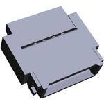
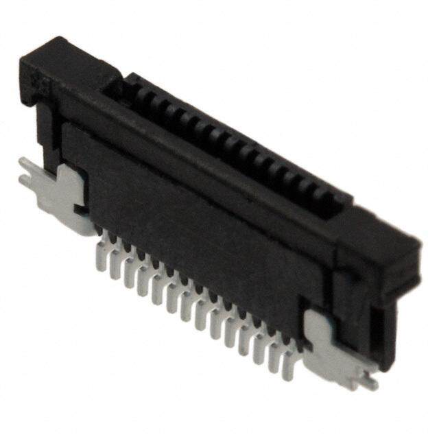
ICGOO电子元器件商城为您提供AYF530435由Panasonic Corporation设计生产,在icgoo商城现货销售,并且可以通过原厂、代理商等渠道进行代购。 AYF530435价格参考¥9.34-¥9.34。Panasonic CorporationAYF530435封装/规格:FFC,FPC(扁平柔性)连接器, 4 位置 FFC,FPC 连接器 触头,上和下 0.020"(0.50mm) 表面贴装,直角。您可以下载AYF530435参考资料、Datasheet数据手册功能说明书,资料中有AYF530435 详细功能的应用电路图电压和使用方法及教程。
Panasonic Electric Works的AYF530435是一种FFC(柔性扁平电缆)连接器,主要用于需要轻薄、高可靠性和高密度连接的电子设备中。该型号适用于柔性印刷电路(FPC)和柔性扁平电缆的连接,具备良好的接触稳定性和耐用性。

其典型应用场景包括:

1. 消费电子产品:如智能手机、平板电脑和笔记本电脑,用于连接显示屏、摄像头模组、触控面板等内部组件;
2. 工业设备:用于自动化控制系统的传感器、人机界面(HMI)及显示模块的连接;
3. 汽车电子:应用于车载显示系统、导航设备、仪表盘模块等对空间和重量有要求的场景;
4. 医疗设备:如便携式监护仪、内窥镜等对连接器有高稳定性和小型化要求的设备;
5. 办公设备:打印机、扫描仪等设备中用于连接移动部件与主板之间的信号传输。

AYF530435具备自对准功能,插拔方便,适用于高振动或频繁插拔的环境,是实现紧凑型电子设备内部高效连接的重要组件。
| 参数 | 数值 |
| 产品目录 | |
| 描述 | CONN SOCKET FPC 0.5MM 4POS SMD |
| 产品分类 | |
| FFC,FCB厚度 | 0.30mm |
| 品牌 | Panasonic Electric Works |
| 数据手册 | |
| 产品图片 |
|
| 产品型号 | AYF530435 |
| rohs | 无铅 / 符合限制有害物质指令(RoHS)规范要求 |
| 产品系列 | Y5B |
| 其它名称 | 255-3056-1 |
| 其它有关文件 | |
| 包装 | 剪切带 (CT) |
| 外壳材料 | 液晶聚合物(LCP) |
| 安装类型 | 表面贴装,直角 |
| 工作温度 | -55°C ~ 85°C |
| 扁平柔性类型 | FFC, FPC |
| 材料可燃性等级 | UL94 V-0 |
| 板上高度 | 0.039"(1.00mm) |
| 标准包装 | 1 |
| 特性 | - |
| 电缆端类型 | 锥形 |
| 端接 | |
| 致动器材料 | 液晶聚合物(LCP) |
| 触头材料 | 铜合金 |
| 触头镀层 | 金 |
| 连接器/触头类型 | 触头,上和下 |
| 针脚数 | 4 |
| 锁定功能 | 翻转锁定,背锁 |
| 间距 | 0.020"(0.50mm) |
| 额定电压 | 50V |
| 额定电流 | 0.5A/触头 |


.jpg)

- 商务部:美国ITC正式对集成电路等产品启动337调查
- 曝三星4nm工艺存在良率问题 高通将骁龙8 Gen1或转产台积电
- 太阳诱电将投资9.5亿元在常州建新厂生产MLCC 预计2023年完工
- 英特尔发布欧洲新工厂建设计划 深化IDM 2.0 战略
- 台积电先进制程称霸业界 有大客户加持明年业绩稳了
- 达到5530亿美元!SIA预计今年全球半导体销售额将创下新高
- 英特尔拟将自动驾驶子公司Mobileye上市 估值或超500亿美元
- 三星加码芯片和SET,合并消费电子和移动部门,撤换高东真等 CEO
- 三星电子宣布重大人事变动 还合并消费电子和移动部门
- 海关总署:前11个月进口集成电路产品价值2.52万亿元 增长14.8%

PDF Datasheet 数据手册内容提取
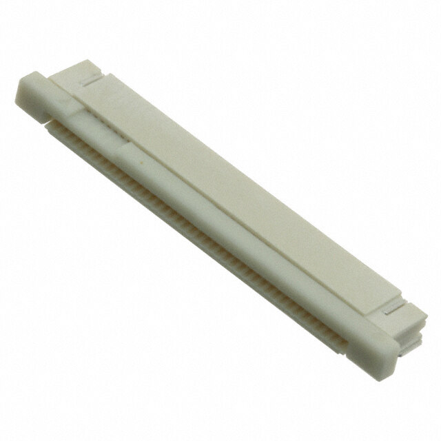
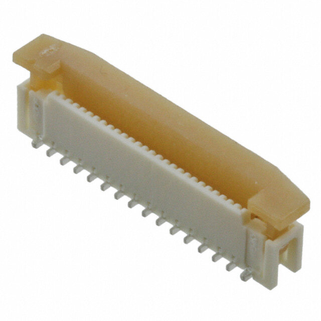
For FPC/FFC FPC/FFC connectors Y5B/Y5BW (0.5mm pitch) Back lock Pitch 0.5 mm, low profile/space saving and double top and bottom contacts construction FEATURES 1. Double top and bottom contacts construction 2. Wiring patterns can be placed under the connector 3. Time and effort can be reduced by delivering with lever open 4. Lock hold type (Y5BW) with excellent holding force is available (Y5BW: support only FPC) 5. Supports high speed transmission standard V-by-One® HS. of THine Electronics, Inc. APPLICATIONS Mobile devices and industrial equipment *V-by-One®HS: An interface for the next- generation high-speed signals developed by THine Electronics, Inc. V-by-One® is a registered trademark of THine Electronics, Inc. DETAILED FEATURES Low profile and space saving design Lock hold type (Y5BW) is also available Low profile and space saving design of 1.0 mm high and 3.20 The FPC holding contacts located on both ends of the connector mm deep (3.70 mm with lever) facilitate positioning of FPC and further enhance the FPC holding force. Applicable FPC shape Structure to lock notches on both 1.00 ends of the FPC 3.20 with soldering terminals With notches 4 pins (Y5B: minimum) Notes:1.The inserted FPC can be temporarily held until the lever is closed. 2.When the lever is closed, the holding contacts lock the FPC by its notches, enhancing the FPC holding force. Prevent displacement of FPC insertion Constructed to make positional displacement difficult by surrounding the four sides on the FPC inlet side with wall molding –1– ACCTB1E 201803-T
Y5B/Y5BW FPC/FFC connectors (0.5mm pitch) ORDERING INFORMATION Y5B AYF 53 3 5 53: 0.5 mm pitch Number Function Surface treatment Back lock of pins 3: Top and bottom (Contact portion / Terminal portion) (2 digits) double contacts 5: Au plating/Au plating Y5BW AYF 53 6 5 T 53: 0.5 mm pitch Number Function Surface treatment Back lock of pins 6: Top and bottom double contacts (Contact portion / Terminal portion) (2 digits) and lock hold type 5: Au plating/Au plating PRODUCT TYPES Y5B Packing Height Number of pins Part number Inner carton (1-reel) Outer carton 4 AYF530435 5 AYF530535 6 AYF530635 8 AYF530835 10 AYF531035 12 AYF531235 14 AYF531435 16 AYF531635 1.0 mm 5,000 pieces 10,000 pieces 24 AYF532435 28 AYF532835 30 AYF533035 32 AYF533235 34 AYF533435 40 AYF534035 42 AYF534235 50 AYF535035 Notes:1.Order unit: For volume production: 1-inner carton (1-reel) units. For samples, please contact our sales office. 2.Please contact our sales office for connectors having a number of pins other than those listed above. –2– ACCTB1E 201803-T
Y5B/Y5BW FPC/FFC connectors (0.5mm pitch) Y5BW Packing Height Number of pins Part number Inner carton (1-reel) Outer carton 2 AYF530265T 3 AYF530365T 4 AYF530465T 6 AYF530665T 8 AYF530865T 10 AYF531065T 12 AYF531265T 14 AYF531465T 1.0 mm 5,000 pieces 10,000 pieces 22 AYF532265T 26 AYF532665T 28 AYF532865T 30 AYF533065T 32 AYF533265T 38 AYF533865T 40 AYF534065T 48 AYF534865T Notes:1.Order unit: For volume production: 1-inner carton (1-reel) units. For samples, please contact our sales office. 2.Please contact our sales office for connectors having a number of pins other than those listed above. SPECIFICATIONS 1. Characteristics The followings show specifications, when using an applicable FPC (thickness 0.30 mm) Item Specifications Conditions Rated current 0.5A/pin contact (except for holding contact) Rated voltage 50V AC/DC No short-circuiting or damage at a detection current of 1 mA Electrical Dielectric strength 250V AC for 1 min. when the specified voltage is applied for one minute. characteristics Insulation resistance Min. 1,000MΩ (initial) Using 250V DC megger (applied for 1 min.) Contact resistance Max. 100mΩ Based on the contact resistance measurement method specified by JIS C 5402. Y5B: Min. 0.2N/pin contact × pin contacts (initial) Measurement of the maximum force applied until the Mechanical FPC holding force Y5BW: Min. 0.2N/pin contact × pin contacts + 2.0N inserted compatible FPC is pulled out in the insertion axis characteristics (initial) direction while the connector lever is closed Ambient temperature –55 to +85°C No icing. No condensation. Reflow soldering: Peak temperature: 260°C or less The initial specification must be satisfied electrically Soldering heat resistance (on the surface of the PC board around the connector and mechanically. terminals) Soldering iron: 300°C within 5 sec. 350°C within 3 sec. –55 to +85°C (product only) Storage temperature –40 to +50°C (emboss packing) No icing. No condensation. Conformed to MIL-STD-202F, method 107G Order Temperature (°C) Time (minutes) Environmental Thermal shock resistance 5in scuyclaletiso,n resistance min. 100MΩ, 12 –55−03 Ma3x0. 5 characteristics (with FPC mated) contact resistance max. 100mΩ 3 85+3 30 0 4 Max. 5 –55−03 120 hours, H(wuitmhi dFiPtyC r emsaistteadn)ce icnosnutlaactito rne sreisstiasntacnec me amxi.n 1. 0100m0MΩΩ, CTeomnfpoerrmaetudr eto 4 I0E±C26°C00, 6h8u-m2-id7i8ty 90 to 95% R.H. 24 hours, S(wailtthw FatPeCr smpraatey dr)esistance icnosnutlaactito rne sreisstiasntacnec me amxi.n 1. 0100m0MΩΩ, CTeomnfpoerrmaetudr eto 3 I5E±C26°C00, 6s8a-lt2w-a1t1er concentration 5±1% H2S resistance 48 hours, Temperature 40±2°C, gas concentration 3±1 ppm, (with FPC mated) contact resistance max. 100mΩ humidity 75 to 80% R.H. Lifetime Insertion and removal life 20 times Repeated insertion and removal: min. 10 sec./time characteristics Unit weight Y5B 50 pins: 0.16 g –3– ACCTB1E 201803-T
Y5B/Y5BW FPC/FFC connectors (0.5mm pitch) 2. Material and surface treatment Part name Material Surface treatment Housing: LCP resin (UL94V-0) Molded portion — Lever: LCP resin (UL94V-0) Contact portion; Base: Ni plating, Surface: Au plating Contact Copper alloy Terminal portion; Base: Ni plating, Surface: Au plating Holding contact (Only Y5BW) Copper alloy Terminal portion; Base: Ni plating, Surface: Au plating Soldering terminal portion Copper alloy Base: Ni plating, Surface: Au plating DIMENSIONS (Unit: mm) The CAD data of the products with a mark can be downloaded from: http://industrial.panasonic.com/ac/e/ Y5B External dimensions A 0.50±0.10 Dimension table Dimensions ±0.10 1(S.6u0c(t3io.7n0 a)rea) Nofu pminbser A B C 0 0 1. 6) 4 4.00 3.36 1.50 7 1. 5 4.50 3.86 2.00 ( 6 5.00 4.36 2.50 Terminal coplanarity (0.30) 8 6.00 5.36 3.50 0.1 (0.50) 10 7.00 6.36 4.50 (Contact and soldering terminals) (((111...555000))) 12 8.00 7.36 5.50 (((FFFPPPCCC iiinnnssseeerrrtttiiiooonnn dddeeepppttthhh))) 14 9.00 8.36 6.50 B±0.20 2.90 (0.15) 3.20 16 10.00 9.36 7.50 24 14.00 13.36 11.50 28 16.00 15.36 13.50 30 17.00 16.36 14.50 32 18.00 17.36 15.50 34 19.00 18.36 16.50 (0.15) 40 22.00 21.36 19.50 ) C±0.20 .32 42 23.00 22.36 20.50 (0 General tolerance: ±0.3 50 27.00 26.36 24.50 Each mentioned sizes are at the stage of initial delivery. Y5B Recommended FPC/FFC dimensions (Finished thickness: t = 0.3±0.03) The conductive parts should be based by Ni plating and then Au plating. Dimension table (A+1)±0.05 Dimensions A±0.03 0.50±0.07 (FPC)0.3 5±0.03 R0.20±0.05 Number A 0.50±0.03 (FFC)0.30±0.03 0.30±0.03 of pins 1.50min.(Conductorexposed area) .50min.orcing plate) 4568 1223....50550000 2einf 10 4.50 (R 12 5.50 14 6.50 Cutting direction※ 16 7.50 ※Cut FPC/FFC from the copper foil side to the reinforcing plate side. 24 11.50 28 13.50 30 14.50 32 15.50 34 16.50 40 19.50 42 20.50 50 24.50 –4– ACCTB1E 201803-T
Y5B/Y5BW FPC/FFC connectors (0.5mm pitch) Y5BW External dimensions A 0.50±0.10 Dimension table Dimensions Holding contacts (The holding contacts 0 (3.70) Number A B C D cannot be used as conductors.) ±0.1 1(S.6u0ction area) of pins 00 2 4.00 3.36 1.50 0.50 1. 76) 3 4.50 3.86 2.00 1.00 . 1 ( 4 5.00 4.36 2.50 1.50 Terminal coplanarity (0.30) 6 6.00 5.36 3.50 2.50 0.1 (0.50) 8 7.00 6.36 4.50 3.50 (Contact, holding contacts and soldering terminals) 10 8.00 7.36 5.50 4.50 (((111...555000))) B±0.20 (((FFFPPPCCC iiinnnssseeerrrtttiiiooonnn dddeeepppttthhh))) 12 9.00 8.36 6.50 5.50 (0.15) 2.90 14 10.00 9.36 7.50 6.50 3.20 22 14.00 13.36 11.50 10.50 26 16.00 15.36 13.50 12.50 28 17.00 16.36 14.50 13.50 30 18.00 17.36 15.50 14.50 (0.15) 32 19.00 18.36 16.50 15.50 D±0.20 ) ) 38 22.00 21.36 19.50 18.50 (0.15) C±0.20 (0.32 (0.32 General tolerance: ±0.3 40 23.00 22.36 20.50 19.50 48 27.00 26.36 24.50 23.50 Each mentioned sizes are at the stage of initial delivery. Y5BW Recommended FPC dimensions (Finished thickness: t = 0.3±0.03) The conductive parts should be based by Ni plating and then Au plating. Dimension table (A+2)±0.05 Dimensions 1.00±0.07 A±0.03 0.70±0.05※1 0.30±0.03 0.50±0.03 (Pitch)0.35±0.03 R0.20±0.05 Number A R0.25max. RR00..2200±±00..00550.80±0.050.80±0.050.80±0.05 1.30±0.10 1.50min(Conductorexposed area) 2.50minnforcing plate) of pins 2346 0112....50550000 R0.25max. Rei 8 3.50 ( 10 4.50 12 5.50 Cutting direction※2 14 6.50 ※1 Not interfere conductor ※1 22 10.50 ※2 Cut FPC from the copper foil side to the reinforcing plate side. 26 12.50 28 13.50 30 14.50 32 15.50 38 18.50 40 19.50 48 23.50 –5– ACCTB1E 201803-T
Y5B/Y5BW FPC/FFC connectors (0.5mm pitch) EMBOSSED TAPE DIMENSIONS (Unit: mm) Specifications for taping Specifications for the plastic reel In accordance with EIAJ ET-7200B. Tape I Tape II (A +- 00..31) (A±0.3) (B) (C) (1.75) (B) D±1 Taping reel (1.75) Top cover tape ng ) ) ction after packagi (2.0)(4.0 (2.0)(4.0 φ380 EEmmbboosssseedd cmaorruienrt itnagp-ehole ding dire (8.0) (8.0) Label a e L φ1.5+ 00.1 φ1.5+ 00.1 Dimension table Y5B Number of pins Type of taping A B C D Quantity per reel 4 to 10 Tape I 16.0 7.5 – 17.4 5,000 12 to 30 Tape I 24.0 11.5 – 25.4 5,000 32 to 34 Tape II 32.0 14.2 28.4 33.4 5,000 40 to 50 Tape II 44.0 20.2 40.4 45.4 5,000 Y5BW Number of pins Type of taping A B C D Quantity per reel 2 to 8 Tape I 16.0 7.5 – 17.4 5,000 10 to 28 Tape I 24.0 11.5 – 25.4 5,000 30 to 32 Tape II 32.0 14.2 28.4 33.4 5,000 38 to 48 Tape II 44.0 20.2 40.4 45.4 5,000 Connector orientation with respect to embossed tape feeding direction Type Direction Y5B/Y5BW of tape progress –6– ACCTB1E 201803-T
Y5B/Y5BW FPC/FFC connectors (0.5mm pitch) NOTES (Unit: mm) Design of PC board patterns Conduct the recommended foot pattern design, in order to preserve the mechanical strength of terminal solder areas. Recommended PC board and metal mask patterns Connectors are mounted with high pitch density, intervals of 0.4 The figures are recommended patterns. Please use them as a mm, 0.5 mm or 0.6 mm. In order to reduce solder and flux rise, reference. solder bridges and other issues make sure the proper levels of solder is used. Recommended PC board pattern Recommended metal mask pattern (mounting layout) Metal mask thickness: When 120μm (Terminal portion opening area ratio: 57%) 5 0.50±0.05 ±0.0 (Metal-part portion opening area ratio: 100%) 0.30±0.05 0 0.8 0.50±0.01 ±0.01 0.25±0.01 5 5 . 0 0.40±0.05 .05.05 1.00±0.05 1.00±0.05 0.80±03.30±0 01..4000±±00..0011 1.00±0.01 0±0.01.30±0.01 .83 0 Please refer to the latest product specifications when designing your product. –7– ACCTB1E 201803-T
Notes on Using FPC/FFC Connectors About safety remarks 1) Do not use these connectors beyond the specification sheets. 3) Panasonic Corporation is consistently striving to improve The usage outside of specified rated current, dielectric strength, quality and reliability. However, the fact remains that electrical and environmental conditions and so on may cause circuitry components and devices generally cause failures at a given damage via abnormal heating, smoke, and fire. statistical probability. Furthermore, their durability varies with 2) In order to avoid accidents, your thorough specification review use environments or use conditions. In this respect, please is appreciated. Please contact our sales office if your usage is check for actual electrical components and devices under actual out of the specifications. Otherwise, Panasonic Corporation conditions before use. cannot guarantee the quality and reliability. Continued usage in a state of degraded condition may cause the deteriorated insulation, thus result in abnormal heat, smoke or firing. Please carry out safety design and periodic maintenance including redundancy design, design for fire spread prevention, and design for malfunction prevention so that no accidents resulting in injury or death, fire accidents, or social damage will be caused as a result of failure of the products or ending life of the products. PC board design 1) Design the recommended foot pattern in order to secure the 4) Y3BW/Y5BW mechanical strength in the soldered areas of the terminal. Depending on FPC/FFC dimension and FPC/FFC insertion 2) In order to facilitate the connector mount, make sure to design location, there is a possibility that the holding contact and an the board with reduced warpage. FPC/FFC pattern of both end of signal contacts are in short- 3) Please design and pay attention to the distance from the circuited. Please design the equipment not to be affected even if board edge to the pattern. When cutting the board, do not give a board pattern of holding contacts and an FPC/FFC pattern of an excessive stress to the connector, which risks damaging the both end of signal contacts are in short-circuited. connector. (For example: Do not connect a board pattern of holding contacts and GND. If connect a board pattern of holding contacts and GND, also connect board pattern of both end of signal contacts.) FPC/FFC and equipment design 1) Design the FPC/FFC based with recommended dimensions 8) Y4BH, Y5BH to ensure the required connector performance. When using in high-speed transmission applications, please 2) When back lock type is used, secure enough space for take care when designing the FPC/FFC, because the differential closing the lever and for open-close operation of the lever. impedance values may be uneven depending on FPC/FFC 3) Make sure that connector positioning and FPC/FFC length dimensions settings, uneven dimensions, and layering are appropriate to prevent diagonal insertion of the FPC/FFC. composition. 4) Due to the FPC/FFC size, weight, or the reaction force of the 9) Y3BW/Y5BW routed FPC/FFC, FPC/FFC removed and connector deformation The holding contacts cannot be used as conductors. may occur by a fall, vibration, or other impact. The holding contacts are located on both ends of the When using FPC/FFC connector for smart phones, cellular connector, and the shape of the soldered portions is the phones and other applications which require falling resistance, same as that of the signal contacts. Use caution to ensure please pay attention to precautions. connect identification. 5) Carefully check the equipment design and take required 10) Y3BL measures to prevent the FPC/FFC removed. Soldering terminal structure 6) If the shock of falling, vibration is applied to the FPC/FFC, • Since soldering terminals touch FPC/FFC, note that the short please design the equipment not to be applied a load to circuit may occur when the metal parts exposed on side of FPC/ connector, such as fixing the FPC/FFC. FFC. 7) Make sure to design the FPC/FFC insertion part with reduced • Depending on FPC/FFC dimension, there is a possibility that warpage. Otherwise, the warpage may adversely affect the FPC/ soldering terminals and an FPC/FFC pattern of both end of FFC insertion. signal contacts are in short-circuited. Please design the equipment not to be affected even if a board pattern of soldering terminals and an FPC/FFC pattern of both end of signal contacts are in short-circuited. (For example: Do not connect a board pattern of soldering terminals and GND. If connect a board pattern of soldering terminals and GND, also connect board pattern of both end of signal contacts.) –1– ACCTB13E 201803-T
Notes on Using FPC/FFC Connectors Connector mounting 1) Excessive mounter chucking force may deform the molded or 2) In case of dry condition, please note the occurrence of static metal part of the connector. Consult us in advance if chucking is electricity. The product may be adhered to the embossed carrier to be applied. tape or the cover tape in dry condition. Recommended humidity is from 40 to 60%RH and please remove static electricity by ionizer in manufacturing process. Soldering 1. Manual soldering 1) As this product is compact size, please avoid the excessive 3) Soldering flux may contaminate the contact portion, please solder. Because the excessive solder makes creepage and flux check the contact portion after soldering with a magnifying wicking at contact portion, or impact contact by soldering glass. If the contamination is found, please clean the interference. contamination before use. 2) Please use the soldering iron under specified temperature 4) As excessive force to terminal by manual soldering has some and times. possibilities of contact portion deformation, please be careful to the force by hand. 5) Please clean soldering iron tip. 2. Reflow soldering 1) When cream solder printing is used, screen method is 8) Infrared reflow soldering is able to passed two times. recommended. 9) The temperature is measured on the PC board surface near 2) To achieve the appropriate soldering state, make sure that the connector terminals. reflow temperature, PC board foot pattern, window size and 10) The condition of solder or flux creepage and wettability thickness of metal mask are recommended condition. depend on the type of solder and flux. Please set the reflow 3) Note that excess solder on the terminals prevents complete temperature and oxygen level by considering the solder and flux insertion of the FPC/FFC, and causes flux climbing up. characteristics. 4) A screen thickness of 120μm is recommended during cream 11) Do not use resin-containing solder. Otherwise, the contacts solder printing. might be firmly fixed. 5) When applying the different thickness of a screen, please 12) When performing reflow soldering on the back of the PC contact our sales office. board after reflow soldering the connector, secure the connector 6) There may be a case of difficult self-alignment depending on using, for example, an adhesive. the connector size. In that case, please be careful to align (Double reflow soldering on the same side is possible.) terminals and solder pads. Do not apply reflow heating while a lever is closing (or on 7) The following diagram shows the recommended reflow the way of closing) soldering temperature profile. The terminals may be deformed by reflow heating with a lever is closing (or on the way of closing). Temperature Peak temperature Peak temperature 260℃ 230℃ 220℃ Preheating 200℃ 180℃ Upper limited 150℃ 25 sec. (Solder heat resistance) 60 to 120 sec. Lower limited 70 sec. (Solder wettability) Time 3. Rework of soldering portion. 1) Rework shall be only one time. 2) Please avoid the supplementary flux in case of rework for soldering bridge, as this may cause flux creepage to contact portion. When adding the solder for reworking, do not add an excessive solder. 3) Please use the soldering iron under specified temperature. 4. As the excessive force on the terminals may cause the 6. When cutting or bending the PC board after mounting the deformation and the integrity of solderability will be lost connector, please avoid the stress at the soldering portion. during reflow soldering, please avoid dropping or rough The soldered areas should not be subjected to force. handling of the product. 5. When the soldering is not completed, do not open/close the lever or insert/ remove an FPC/FFC. And the external compulsory force to the terminal may cause the fixing force lowering between the terminal and the molding or the coplanarity failures. In addition, do not insert an FPC/FFC into the connector before soldering the connector. –2– ACCTB13E 201803-T
Notes on Using FPC/FFC Connectors PC board 1) As thick coverlay/solder resist and adhesive may cause poor soldering, please set thickness of coverlay and adhesive as thin as possible. Precautions for insertion/removal of FPC/FFC 1) (Except for Y3BC) 9) To close the lever, turn down the lever by pressing the entire Avoid touching the lever (applying any external force) until an lever or both sides of the lever with fingers tips. And close the FPC/FFC is inserted. Do not open/close the lever without an lever completely. Be careful not to apply partial load to the lever FPC/FFC inserted. Failure to follow this instruction will cause that may cause its deformation or destruction or lever going back the contacts to warp, leading to the contact tips to interfere with to initial position. Close the lever completely to prevent contact the insertion of an FPC/FFC, deforming the terminals. Failure to failure. follow this instruction may cause the lever to be removed, 10) Avoid applying an excessive load to the top of the lever terminals to be deformed, and/or the FPC/FFC insertion force to during or after closing the lever. Otherwise, the terminals may be increase. deformed. 11) When opening the lever to remove the FPC/FFC, rotate the Without an FPC inserted lever to the initial position. Do not push the lever into the FPC/ FFC inlet side and ensure that the lever will not go over the initial position; otherwise, it may be deformed or broken. 12) To open the lever, if pressure to the lever is applied unevenly, 2) These connectors are of the back lock type, which has the such as to an edge only, it may deform or break. FPC/FFC insertion section on the opposite side of the lever. Be 13) Do not open the lever forcefully with something sharp tool, careful not to make a mistake in the FPC/FFC insertion position otherwise, the lever may be deformed. or the lever opening/closing position. Otherwise, a contact failure 14) Remove the FPC/FFC at parallel with the lever fully opened. or connector breakage may occur. If the lever is closed, or if the FPC/FFC is forcedly pulled, the 3) Do not insert an FPC/FFC upside down. Inserting an FPC/ product or FPC/FFC may break. FFC in a direction opposite to that you intended may cause an 15) If a lever is accidentally detached during the handling of a operation failure or malfunction. connector, do not use the connector any longer. 4) Insert an FPC/FFC with the lever opened at right angle, that 1. After an FPC/FFC is inserted, carefully handle it so as not is, in the factory default position. to apply excessive stress to the base of the FPC/FFC. When 5) After checking the position of FPC/FFC insertion slot and using FPC/FFC with a bent condition, please pay attention FPC/FFC, completely insert the FPC/FFC horizontally to the full to precautions below; otherwise, in some conditions it may depth of the connector without altering the angle. An FPC/FFC cause conduction failure, connector breakage, unlocking inserted at an excessive angle to the board may cause the lever or FPC/FFC disconnection. deformation of metal parts, crack of molding parts, FPC/FFC 16) Design so that a load is not applied to connector directly by insertion failures, and FPC/FFC circuit breakages. FPC/FFC bending. 17) Avoid sharp FPC/FFC bending at the root of FPC/FFC insertion part. 18) Design so that a load is not applied to the part of FPC/FFC bending. 19) If there might be a load on FPC/FFC, please fix the FPC/ FFC. 20) Y3BW and Y5BW 6) Insert the FPC/FFC into the connector after checking the Fix the FPC/FFC if there might be a load to the cut out, do not position of FPC/FFC insertion slot and FPC/FFC. Do not insert apply bending load to the cutout part of FPC/FFC. Otherwise, it the FPC/FFC without positioning the FPC/FFC and connector. may cause FPC/FFC disconnection and deformation since the Otherwise, it may cause connector breakages. When it is hard to cutout part of FPC/FFC is subjected to bending stress. insert the FPC/FFC, do not insert the FPC/FFC on that condition. Confirm the FPC/FFC and connector positioning. 7) Do not apply an excessive load to the lever in the opening direction beyond its open position; otherwise, the lever may be deformed or removed. 8) Do not apply an excessive load to the lever in a direction perpendicular to the lever rotation axis or in the lever opening direction; otherwise, the terminals may be deformed, and the lever may be removed. FPC/FFC cutout part –3– ACCTB13E 201803-T
Notes on Using FPC/FFC Connectors Cleaning treatment Cleaning this product is not needed basically. 1) Please keep the cleanliness of the cleaning fluid to make sure Please note the following points to prevent the negative effect to that the contact surfaces are not contaminated by the cleaning the product when cleaning is necessary. fluid itself. 2) Semi-aqueous cleaning solvent is recommended as some powerful solvent may dissolve the molding portion or the marked letters. Please contact our sales office when other solvent is used. Precautions for operating environment and storage environment 1) Panasonic Corporation does not guarantee the failures caused by condensation. Other precautions 1) When the coating material is used for preventing PC board 5) The detailed shape of metal parts and molding parts may isolation deterioration after soldering, please assure the coating differ depending on the mold. material is not adhered on any part of connector. 6) Height in FPC/FFC mating depends on the way to being used, 2) Please avoid the usage of connector as electric switching such as mounting condition, thickness of FPC/FFC, and angle of basically. lever lock etc. Please check it by actual equipment. 3) There is no problem on the product quality though the swelling, the black spot, the small scars and the foreign matter, etc. might be generated in the molding parts. 4) There is no problem on the product quality though the weld line might be generated in the weld part of molding parts when the use of product is within the specifications. Please refer to the latest product specifications when designing your product. –4– ACCTB13E 201803-T
None
Mouser Electronics Authorized Distributor Click to View Pricing, Inventory, Delivery & Lifecycle Information: P anasonic: AYF530265 AYF530365 AYF530435 AYF530465 AYF530535 AYF530565 AYF530635 AYF530665 AYF530735 AYF530765 AYF530835 AYF530865 AYF530935 AYF530965 AYF531035 AYF531065 AYF531135 AYF531165 AYF531235 AYF531265 AYF531335 AYF531365 AYF531435 AYF531465 AYF531535 AYF531565 AYF531635 AYF531665 AYF531735 AYF531765 AYF531835 AYF531865 AYF531935 AYF531965 AYF532035 AYF532065 AYF532135 AYF532165 AYF532235 AYF532265 AYF532335 AYF532365 AYF532435 AYF532465 AYF532535 AYF532565 AYF532635 AYF532665 AYF532735 AYF532765 AYF532835 AYF532865 AYF532935 AYF532965 AYF533035 AYF533065 AYF533135 AYF533165 AYF533235 AYF533265 AYF533335 AYF533365 AYF533435 AYF533465 AYF533535 AYF533565 AYF533635 AYF533665 AYF533735 AYF533765 AYF533835 AYF533865 AYF533935 AYF534035 AYF534065 AYF534135 AYF534165 AYF534235 AYF534265 AYF534335 AYF534365 AYF534435 AYF534465 AYF534535 AYF534565 AYF534635 AYF534665 AYF534735 AYF534765 AYF534835 AYF534865 AYF534935 AYF534965 AYF535035 AYF535065 AYF532665T AYF531065T AYF532865T AYF530665T AYF530365T