ICGOO在线商城 > 连接器,互连器件 > FFC,FPC(扁平柔性)连接器 > AYF312515
 Datasheet下载
- 型号: AYF312515
- 制造商: Panasonic Corporation
- 库位|库存: xxxx|xxxx
- 要求:
| 数量阶梯 | 香港交货 | 国内含税 |
| +xxxx | $xxxx | ¥xxxx |
查看当月历史价格
查看今年历史价格
AYF312515产品简介:
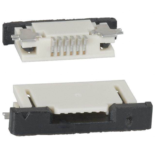
ICGOO电子元器件商城为您提供AYF312515由Panasonic Corporation设计生产,在icgoo商城现货销售,并且可以通过原厂、代理商等渠道进行代购。 AYF312515价格参考。Panasonic CorporationAYF312515封装/规格:FFC,FPC(扁平柔性)连接器, 25 位置 FPC 连接器 触点,底部 0.012"(0.30mm) 表面贴装,直角。您可以下载AYF312515参考资料、Datasheet数据手册功能说明书,资料中有AYF312515 详细功能的应用电路图电压和使用方法及教程。
Panasonic Electric Works的AYF312515是一种FFC(柔性扁平电缆)连接器,广泛应用于需要轻薄、高可靠性和高密度连接的电子设备中。该连接器具备良好的电气性能和机械稳定性,适用于需要频繁插拔或空间受限的场合。

主要应用场景包括:

1. 消费电子产品:如智能手机、平板电脑、笔记本电脑等,用于主板与显示屏、摄像头、触控面板等组件之间的内部连接。

2. 工业设备:用于工业自动化设备、测量仪器、控制面板等中,提供稳定可靠的信号传输。

3. 汽车电子:应用于车载显示系统、导航设备、摄像头模块等,满足汽车环境中对振动和温度变化的耐受要求。

4. 医疗设备:如便携式监测仪、超声设备等,因其小型化和高可靠性,适合对安全性要求高的医疗场景。

5. 办公设备:如打印机、扫描仪、复印机等,用于连接运动部件与主控板,实现灵活布线。

该连接器为1.0mm间距,插拔寿命长,支持表面贴装技术(SMT),便于自动化生产,是现代电子产品中常用的连接解决方案。
| 参数 | 数值 |
| 产品目录 | |
| 描述 | CONN SOCKET FPC 0.3MM 25POS SMD |
| 产品分类 | |
| FFC,FCB厚度 | 0.20mm |
| 品牌 | Panasonic Electric Works |
| 数据手册 | 点击此处下载产品Datasheethttp://pewa.panasonic.com/assets/pcsd/catalog/y5b-catalog.pdf#page=5 |
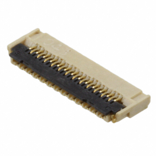
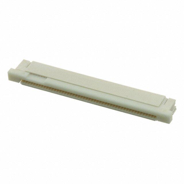
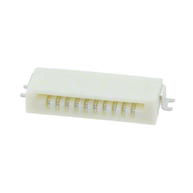
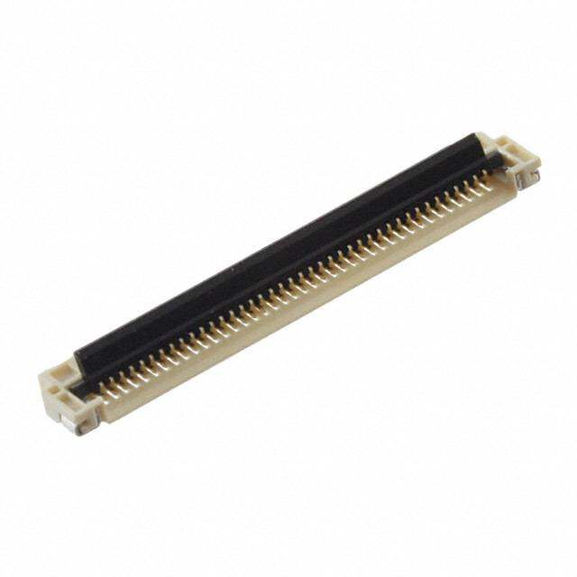
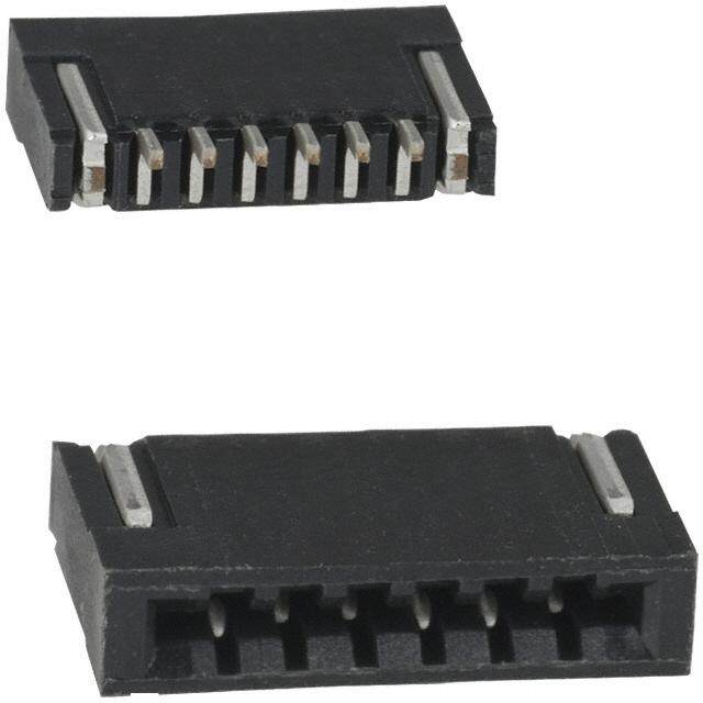
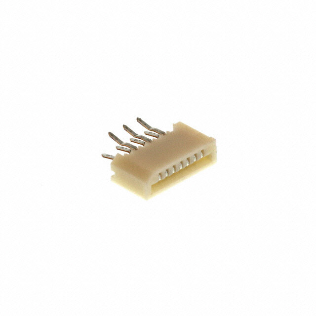
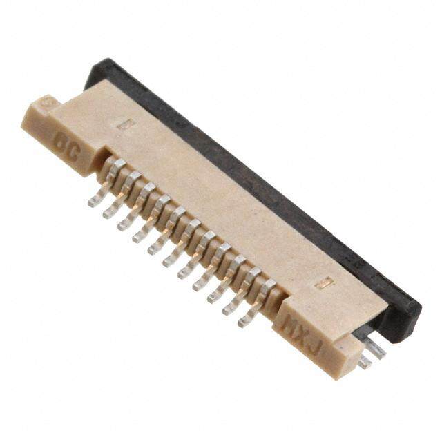
| 产品图片 |
|
| 产品型号 | AYF312515 |
| PCN过时产品 | |
| rohs | 无铅 / 符合限制有害物质指令(RoHS)规范要求 |
| 产品系列 | Y3FT |
| 其它名称 | 255-3047-2 |
| 其它有关文件 | |
| 包装 | 剪切带 (CT) |
| 外壳材料 | 液晶聚合物(LCP) |
| 安装类型 | 表面贴装,直角 |
| 工作温度 | -55°C ~ 85°C |
| 扁平柔性类型 | FPC |
| 材料可燃性等级 | UL94 V-0 |
| 板上高度 | 0.036"(0.90mm) |
| 标准包装 | 1,000 |
| 特性 | 零插入力(ZIF) |
| 电缆端类型 | 焊片式 |
| 端接 | |
| 致动器材料 | 液晶聚合物(LCP) |
| 触头材料 | 铜合金 |
| 触头镀层 | 金 |
| 连接器/触头类型 | 触点, 底部 |
| 针脚数 | 25 |
| 锁定功能 | 触发锁 |
| 间距 | 0.012"(0.30mm) |
| 额定电压 | 50V |
| 额定电流 | 0.2A/触头 |


.jpg)
.jpg)

.jpg)
PDF Datasheet 数据手册内容提取
Automation Controls Catalog For FPC To Be Discontinued Last time buy:September 30, 2014 FPC connectors Y3FT (0.3mm pitch) Series Front lock with FPC tabs FEATURES 1.Low-profile, space-saving design 3.Soldering terminals for higher (pitch: 0.3mm) mounting strength The 0.9mm height, 3.0mm depth 4.Easy-to-handle front lock structure contributes to the miniaturization and 5. Wiring patterns can be placed thickness reduction of target products. underneath the connector. 6.Ni barrier with high resistance to * The total depth including the lever is 3.2mm. solder creep APPLICATIONS Mobile devices, such as cellular phones, smartphones, digital still 0.9 cameras and digital video cameras. 3.0 Unit: mm 2.FPC with tabs ensures high reliability through secure connectibility Thanks to a design in which the FPC tab portion attaches to the protruding resin part, depth is reduced making the product more compact. Also makes it possible to securely position the FPC during insertion and prevent diagonal insertion. (Y3F is compatible with FPC without tabs.) FPC tabs to prevent diagonal insertion and ensure reliable holding RoHS compliant Soldering terminals resistant to twisting ORDERING INFORMATION AYF 3 1 1 5 31: FPC Connector 0.3 mm pitch (Front lock, ZIF type with FPC tabs) Number of pins (2 digits) Contact direction 1: Bottom contact Surface treatment (Contact portion / Terminal portion) 5: Au plating/Au plating (Ni barrier) 2013.09 industrial.panasonic.com/ac/e/ –1– ©Panasonic Corporation 2013 ACCTB9E 201309-T
To Be Discontinued AYF31 Last time buy:September 30, 2014 PRODUCT TYPES Packing Height Number of pins Part number Inner carton Outer carton 11 AYF311115 13 AYF311315 15 AYF311515 17 AYF311715 23 AYF312315 25 AYF312515 27 AYF312715 0.9 mm 29 AYF312915 5,000 pieces 10,000 pieces 31 AYF313115 33 AYF313315 35 AYF313515 39 AYF313915 41 AYF314115 45 AYF314515 51 AYF315115 Notes:1.Order unit; For volume production: 1-inner carton (1-reel) units Samples for mounting check: 50-connector units. Please contact our sales offic . Samples: Small lot orders are possible. Please contact our sales offic . 2.Please contact our sales office or connectors having a number of pins other than those listed above. SPECIFICATIONS 1.Characteristics Item Specification Conditions Rated current 0.2A/pin contact Rated voltage 50V AC/DC Insulation resistance Min. 1,000MΩ (initial) Using 250V DC megger (applied for 1 min.) Electrical characteristics Breakdown voltage 150V AC for 1 min. No short-circuiting or damage at a detection current of 1 mA when the specified oltage is applied for one minute. Contact resistance Max. 80mΩ Based on the contact resistance measurement method specified y JIS C 5402. Measurement of the maximum force applied until the Mechanical FPC holding force Min. 0.23N/pin contacts × pin contacts (initial) inserted compatible FPC is pulled out in the insertion axis characteristics direction while the connector lever is closed Ambient temperature –55°C to +85°C –55°C to +85°C (product only) No freezing at low temperatures. No dew condensation. Storage temperature –40°C to +50°C (emboss packing) Conformed to MIL-STD-202F, method 107G Order Temperature (°C) Time (minutes) Thermal shock resistance 5in scuyclaletiso,n resistance min. 100MΩ, 12 –55−03 Ma3x0. 5 (with FPC mated) contact resistance max. 80mΩ 3 85+30 30 4 Max. 5 Environmental –55−03 characteristics Humidity resistance 1in2s0u lhaotiuorns ,resistance min. 100MΩ, Bath temperature 40±2°C, (with FPC mated) contact resistance max. 80mΩ humidity 90 to 95% R.H. S(wailtthw FatPeCr smpraatey dr)esistance 2icno4sn uhtlaoacutitro srne, sreisstiasntacnec me amxi.n 8. 01m00ΩMΩ, Bsaaltthw atetemr pceornactuernet r3a5ti±o2n° 5C±,1% H2S resistance 48 hours, Bath temperature 40±2°C, gas concentration 3±1 ppm, (with FPC mated) contact resistance max. 80mΩ humidity 75 to 80% R.H. Peak temperature: 260°C or less Refl w soldering Soldering heat resistance 300°C within 5 sec. 350°C within 3 sec. Soldering iron Lifetime Insertion and removal life 30 times Repeated insertion and removal: min. 10 sec./time characteristics Unit weight 51 pin contact type: 0.09 g 2.Material and surface treatment Part name Material Surface treatment Housing: LCP resin (UL94V-0) Molded portion — Lever: LCP resin (UL94V-0) Contact portion; Base: Ni plating, Surface: Au plating Contact Copper alloy Terminal portion; Base: Ni plating, Surface: Au plating Soldering terminals portion Copper alloy Base: Ni plating, Surface: Au plating Panasonic Corporation Automation Controls Buisiness Division industrial.panasonic.com/ac/e/ –2– ©Panasonic Corporation 2013 ACCTB9E 201309-T
To Be Discontinued Last time buy:September 30, 2014 AYF31 DIMENSIONS (Unit: mm) 0.60±0.10 (TeArminal pitch) (140°) 50) General tolerance: ±0.3 1. ( When the lever is opened a) Number of pins/ e A B C D ar dimension n Suctio 00..6300±±00..1100 ((TCeornmtaincat lp pitictchh)) 0.10 1131 55..9355 32..0400 33..6000 54..0400 1.12 ( 3.20 ±0.90 15 6.55 3.60 4.20 5.60 17 7.15 4.20 4.80 6.20 23 8.95 6.00 6.60 8.00 Terminal coplanarity 0.20 (0.30) 25 9.55 6.60 7.20 8.60 0.1 (2.07) (Contact and 3.00 (inFsPeCrt ion 27 10.15 7.20 7.80 9.20 D±0.20 soldering terminals) depth) 29 10.75 7.80 8.40 9.80 C±0.20 (0.15) 53) 31 11.35 8.40 9.00 10.40 (0.12) (0. 33 11.95 9.00 9.60 11.00 35 12.55 9.60 10.20 11.60 39 13.75 10.80 11.40 12.80 41 14.35 11.40 12.00 13.40 45 15.55 12.60 13.20 14.60 (0.12) B±0.20 0.30) 51 17.35 14.40 15.00 16.40 ( RECOMMENDED FPC DIMENSIONS (Finished thickness: t = 0.2±0.03) The conductive parts should be based by Ni plating and then Au plating. A±0.1 Number of pins/ A B C D B±0.05 dimension 00..3600±±00..0072 C±00.0.330+–00..0043(Contact width) 1131 44..7100 43..2600 33..6000 32..0400 0.30±0.02 (0.10) 00 15 5.30 4.80 4.20 3.60 0.20 max.R0.20 0.30±0.07 ±0.800.1±1.530.1 onductor) 0.20±0.03 2137 75..7900 57..4200 46..8600 46..2000 ±1.700.15±1.600.15±1.500.15±1.050.15±0.850.15 R0C.01.025 0.60±0.02 0.10 max. ±0.480.15 ±2.200.30Cu(Exposed part of the ctting direc3.50 min.tio(Reinforcing plate)n 23322337155939 11 11 0180289.......13975350000000 11 1 7902908.......80206840000000 1 1 1789097.......42462080000000 1 0679987.......86806420000000 00.2.200±±00.0.022 Ctou tth FeP rCei nfrfoormci nthge p claotpep seird feo.il side 41 13.10 12.60 12.00 11.40 0.30+–00..0043(Contact width) 45 14.30 13.80 13.20 12.60 0.60±0.07 D±0.03 0.60±0.07 51 16.10 15.60 15.00 14.40 EMBOSSED TAPE DIMENSIONS (Unit: mm) (Common for respective contact type) •Specifications for taping •Specifications for the plastic reel (In accordance with EIAJ ET-7200B.) Tape I Tape II ng (A±0.30) 1.50+0.10. 0dia. (A±0.30) 1.50+0.10. 0dia. (C±1) Taping reel ackagi (2.0)(4.0) (2.0)(4.0) Top cover tape p g direction after (8.0) (8.0) 380 dia. EEmmbboosssseedd cmaorruinetri ntagp-heole din Label a e L (B) (1.75) (B) (1.75) (28.40) •Dimension table (Unit: mm) Number of pins Type of taping A B C Quantity per reel Max. 17 Tape I 16.00 7.50 17.40 5,000 23 to 45 Tape I 24.00 11.50 25.40 5,000 51 Tape II 32.00 14.20 33.40 5,000 Panasonic Corporation Automation Controls Buisiness Division industrial.panasonic.com/ac/e/ –3– ©Panasonic Corporation 2013 ACCTB9E 201309-T
To Be Discontinued AYF31 Last time buy:September 30, 2014 •Connector orientation with respect to embossed tape feeding direction Type Direction Y3FT of tape progress NOTES 1.Recommended PC board and metal Please refer to the latest product mask patterns specifications when designing our Connectors are mounted with high pitch product. density, intervals of 0.3 mm or 0.5 mm. In order to reduce solder and flux ise, solder bridges and other issues make sure the proper levels of solder is used. The figuresto the right are recommended metal mask patterns. Please use them as a reference. Recommended PC board pattern (mounting layout) (TOP VIEW) 3 0 0.03 0.03 00..3600±±00..0033 ±0.500. ±0.600.40±0.10 ±0.03 0 2 3 3. 0 00..4750±±00..0033 00..3600±±00..0033 ±700. Area of exposed Area of exposed 0. soldering terminal soldering terminal Recommended metal mask pattern Metal mask thickness: When 120µm (Front terminal portion opening area ratio: 50%) (Back terminal portion opening area ratio: 51%) (Soldering terminal portion opening area ratio: 100%) 11 00 ±0.01±50.01 00..2670±±00..0011 (0.29) ±2.260.±2.940. 05 60 0.0. 00..4750±±00..0011 00..2670±±00..0011 (0.39) Panasonic Corporation Automation Controls Buisiness Division industrial.panasonic.com/ac/e/ –4– ©Panasonic Corporation 2013 ACCTB9E 201309-T
Notes on Using FPC Connectors Notes on Using FPC Connectors ■ PC board design • Consult us when using a screen-printing thickness other than • Design the recommended foot pattern in order to secure the that recommended. mechanical strength in the soldered areas of the terminal. • Depending on the size of the connector being used, self • In order to facilitate the connector mount, make sure to design alignment may not be possible. Accordingly, carefully position the board with reduced warpage. the terminal with the PC board pattern. • Please design and pay attention to the distance from the board • The recommended reflow temperature profile is given in the edge to the pattern. When cutting the v-cut board, do not give an figure below. excessive stress to the connector, which risks damaging the Upper limit (Soldering heat resistance) connector. Lower limit (Solder wettability) Temperature ■ FPC and equipment design 260°C Peak temperature • Design the FPC based with recommended dimensions to 230°C 220°C ensure the required connector performance. 180°C Preheating 200°C • When using back lock type, secure enough space for closing 150°C 25 sec. 60 to 120 sec. 70 sec. the lever and for open-close operation of the lever. • Make sure that connector positioning and FPC length are Time appropriate to prevent diagonal insertion of the FPC. Due to the FPC size, weight, or the reaction force of the routed FPC, FPC • The temperature is measured on the surface of the PC board may be removed. Carefully check the equipment design. Take near the connector terminals. required measures to prevent the FPC from being removed due • Depending on reflow condition, poor contact may occur by to a fall, vibration, or other impact. solder and flux wicking. • Make sure to design the FPC insertion part with reduced Please set the reflow conditions that considering the warpage. Otherwise, the warpage may adversely affect the FPC characteristics of solder and flux. Also please make insertion. consideration in setting the reflow times and O2 concentration to prevent poor contact by solder and flux wicking. (Y3BW/Y5BW) • When performing reflow soldering on the back of the PC board ■ The holding contacts cannot be used as conductors. after reflow soldering the connector, secure the connector using, The holding contacts are located on both ends of the contacts, for example, an adhesive. and the shape of the soldered portions is the same as that of the (Double reflow soldering on the same side is possible.) other contacts. Do not touch the lever or apply any load to the lever until the Use caution to ensure connect identification. second reflow soldering. Otherwise, contact deflection occurs and the terminals may be deformed by reflow heating. (Y3BL) 3) Reworking on a soldered portion ■ Soldering terminal structure • Finish reworking in one operation. Since soldering terminals touch FPC, note that the short circuit • For reworking of the solder bridge, use a soldering iron with a may occur when the metal parts exposed on side of FPC. flat tip. Do not add flux, otherwise the flux may creep to the contact ■ Connector mounting parts. Excessive mounter chucking force may deform the molded or When adding the solder for reworking, do not add an excessive metal part of the connector. Consult us in advance if chucking is solder. Otherwise, solder and flux may creep up and solder to be applied. bridges may occur. ■ Soldering • Use a soldering iron whose tip temperature is within the 1) Manual soldering temperature range specified in the specifications. • Due to the connector’s compact size, if an excessive amount of solder is applied during manual soldering, the solder may creep ■ Do not drop or handle the connector carelessly. up and flux wicking near the contact points, or solder Otherwise, the terminals may become deformed due to interference may cause contact failure. excessive force or applied solderability may be during • Make sure that the soldering iron tip is heated within the reflow degrade. temperature and time limits indicated in the specifications. ■ Do not open/close the lever or insert/remove an FPC until • Flux from the solder wire may adhere to the contact surfaces the connector is soldered. Forcibly applied external during soldering operations. After soldering, carefully check the pressure on the terminals can weaken the adherence of the contact surfaces and cleans off any flux solder use. terminals to the molded part or cause the terminals to lose • Be aware that a load applied to the connector terminals while their evenness. In addition, do not insert an FPC into the soldering may displace the contact. connector before soldering the connector. • Thoroughly clean the iron tip. ■ When cutting or bending the PC board after mounting the 2) Reflow soldering connector, be careful that the soldered sections are • Screen-printing is recommended for printing paste solder. subjected to excessive force. • To achieve the appropriate soldering state, make sure that the The soldered areas should not be subjected to force. reflow temperature, PC board foot pattern, window size and thickness of metal mask are recommended condition. • Note that excess solder on the terminals prevents complete insertion of the FPC, and causes flux climbing up. • A screen thickness of 120µm is recommended during cream solder printing. Panasonic Corporation Automation Controls Buisiness Division industrial.panasonic.com/ac/e/ –5– ©Panasonic Corporation 2013 ACCTB13E 201306-T
Notes on Using FPC Connectors ■ Precautions for insertion/removal of FPC <Back-Lock> <Front-Lock> • Avoid touching the lever (applying any external force) until an • To open the lever, hold its center and pull it up. An uneven load FPC is inserted. applied to the lever on one side may deform and break the lever. Do not open/close the lever without an FPC inserted. Failure to Do not apply an excessive load to the lever in the opening follow this instruction will cause the contacts to warp, leading to direction, otherwise, the terminals may be deformed. the contact tips to interfere with the insertion of an FPC, • Don’t further apply an excessive load to the fully opened lever; deforming the terminals. Failure to follow this instruction may otherwise, the lever may be deformed. cause the lever to be removed, terminals to be deformed, and/or • Fully open the lever to insert an FPC. the FPC insertion force to increase. • Since this product connects at the bottom, please insert the FPC so that its electrode plane is facing the board to which it will Without an FPC inserted be mounted. Do not insert the FPC in the reverse direction of the contact section; otherwise, operation failures or malfunctions may be caused. (140°) • The FPC insertion section is on the opposite side of the lever. Be careful not to make a mistake in the FPC insertion position or the lever opening/closing position. Otherwise, a contact failure or connector breakage may occur. • Do not insert an FPC upside down. Inserting an FPC in a direction opposite to that you intended may cause an operation (Y3FT) failure or malfunction. • This product has a structure to position an inserted FPC using • Insert an FPC with the lever opened at right angle, that is, in the FPC tabs. the factory default position. Therefore, insert an FPC at an angle to the board. If the FPC is • After checking the position of FPC insertion slot and FPC, inserted in the direction parallel to the board, the molded completely insert the FPC horizontally to the full depth of the positioning parts block the FPC, leading to incomplete insertion. connector without altering the angle. Do not insert the FPC at an excessive angle to the board. An FPC inserted at an excessive angle to the board may cause Otherwise, it may cause the deformation of metal parts, FPC the deformation of metal parts, crack of molding parts, FPC insertion failures, and FPC circuit breakages. insertion failures, and FPC circuit breakages. FPC FPC positioning part • Insert the FPC into the connector after checking the position of (Y3F) FPC insertion slot and FPC. Do not insert the FPC without • Completely insert the FPC horizontally. Do not insert the FPC positioning the FPC and connector. Otherwise, it may cause at an excessive angle to the board. Otherwise, it may cause the connector breakages. When it is hard to insert the FPC, do not deformation of metal parts, FPC insertion failures, and FPC insert the FPC on that condition. Confirm the FPC and circuit breakages. connector positioning. • Do not apply an excessive load to the lever in the opening direction beyond its open position; otherwise, the lever may be deformed or removed. • Do not apply an excessive load to the lever in a direction FPC perpendicular to the lever rotation axis or in the lever opening direction; otherwise, the terminals may be deformed, and the lever may be removed. • Insert the FPC to the full depth of the connector without altering the angle. • When closing the lever, carefully use the tip of your finger to push the entire lever or both sides of it. If pressure to the lever is applied unevenly, IE: only the edge, it may deform or break the FPC. Make sure that the lever is closed completely. Not doing so will cause a faulty connection. • Avoid applying an excessive load to the top of the lever during or after closing the lever. Otherwise, the terminals may be deformed. • Remove the FPC at an angle with the lever fully opened. If the lever is closed, or if the FPC is forcedly pulled into a direction parallel to the board, the molded part may break. Panasonic Corporation Automation Controls Buisiness Division industrial.panasonic.com/ac/e/ –6– ©Panasonic Corporation 2013 ACCTB13E 201306-T
Notes on Using FPC Connectors • To close the lever, turn down the lever by pressing the entire lever or both sides of the lever with fingers tips. And close the lever completely. Be careful not to apply partial load to the lever that may cause its deformation or destruction or lever going back to initial position. Close the lever completely to prevent contact failure. • If pressure to the lever is applied unevenly, it may deform or break the FPC. Make sure that the lever is closed completely. Not doing so will cause a faulty connection. • Avoid applying an excessive load to the top of the lever during or after closing the lever. Otherwise, the terminals may be deformed. • When opening the lever to remove the FPC, rotate the lever to the initial position. Do not push the lever into the FPC inlet side and ensure that the lever will not go over the initial position; otherwise, it may be deformed or broken. • To open the lever, if pressure to the lever is applied unevenly, such as to an edge only, it may deform or break. • Do not open the lever forcefully with something sharp tool, otherwise, the lever may be deformed. • Remove the FPC at parallel with the lever fully opened. If the lever is closed, or if the FPC is forcedly pulled, the product or FPC may break. • If a lever is accidentally detached during the handling of a connector, do not use the connector any longer. ■ After an FPC is inserted, carefully handle it so as not to apply excessive stress to the base of the FPC. When using FPC with a bent condition, please pay attention to precautions below; otherwise, in some conditions it may cause conduction failure, connector breakage, unlocking lever or FPC disconnection. • Design so that a load is not applied to connector directly by FPC bending. • Avoid sharp FPC bending at the root of FPC insertion part. • Design so that a load is not applied to the part of FPC bending. • Fix the FPC if there might be a load on FPC when using the FPC with cutout, do not apply a bending load to the cutout part of FPC. Otherwise, it may cause FPC disconnection and deformation since the cutout part of FPC is subjected to bending stress. FPC cutout part ■ Other cautions • When coating the PC board after soldering the connector (to prevent the deterioration of insulation), perform the coating in such a way so that the coating does not get on the connector. • The connectors are not meant to be used for switching. • There is no problem on the product quality though the swelling and the black spot, etc. might be generated in the molding parts. Please refer to the latest product specifications when designing your product. Panasonic Corporation Automation Controls Buisiness Division industrial.panasonic.com/ac/e/ –7– ©Panasonic Corporation 2013 ACCTB13E 201306-T