ICGOO在线商城 > 电路保护 > TVS - 变阻器,MOV > AVRL101A1R1NTA

 Datasheet下载
- 型号: AVRL101A1R1NTA
- 制造商: TDK
- 库位|库存: xxxx|xxxx
- 要求:
| 数量阶梯 | 香港交货 | 国内含税 |
| +xxxx | $xxxx | ¥xxxx |
查看当月历史价格
查看今年历史价格
AVRL101A1R1NTA产品简介:
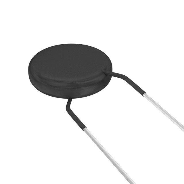
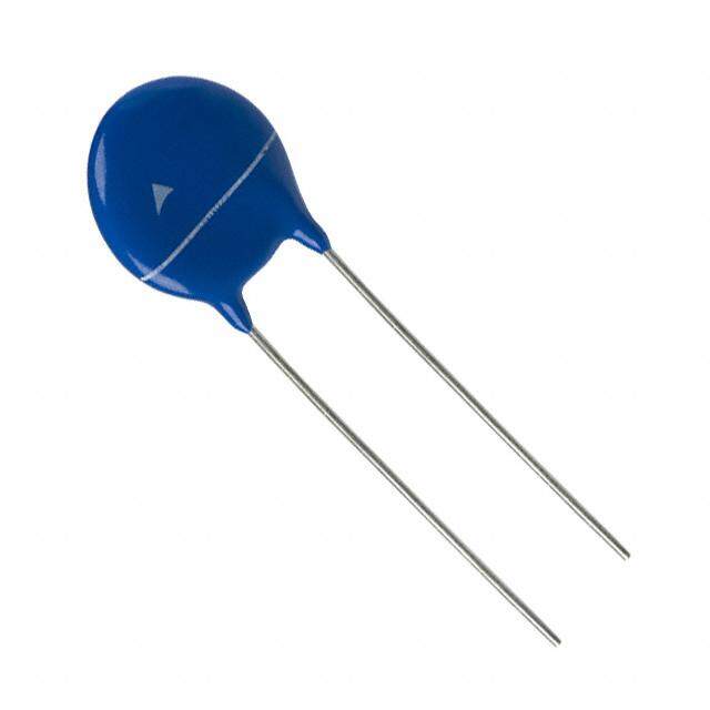
ICGOO电子元器件商城为您提供AVRL101A1R1NTA由TDK设计生产,在icgoo商城现货销售,并且可以通过原厂、代理商等渠道进行代购。 AVRL101A1R1NTA价格参考¥0.38-¥2.64。TDKAVRL101A1R1NTA封装/规格:TVS - 变阻器,MOV, 90V Varistor 1 Circuit Surface Mount, MLCV 0402 (1005 Metric)。您可以下载AVRL101A1R1NTA参考资料、Datasheet数据手册功能说明书,资料中有AVRL101A1R1NTA 详细功能的应用电路图电压和使用方法及教程。
TDK Corporation的AVRL101A1R1NTA是一款压敏电阻(MOV,金属氧化物压敏电阻),属于TVS(瞬态电压抑制)器件的一种。该型号主要用于电路中的过电压保护,特别适用于抑制瞬态浪涌电压,如雷击感应、电感负载切换或静电放电(ESD)等引起的电压尖峰。

典型应用场景包括:消费类电子产品(如电视、机顶盒、路由器等)的电源输入端口保护;工业控制设备的电源线路防护;通信设备中的信号与电源接口防浪涌设计;以及家用电器(如空调、洗衣机)中的电源模块保护。其额定电压为1.1kV,具备良好的能量吸收能力和响应速度,能在瞬态高压出现时迅速导通,将多余能量泄放到地,从而保护后级敏感电子元件。

此外,AVRL101A1R1NTA采用径向引线结构,适合通孔安装,具有较高的可靠性和稳定性,广泛应用于需要符合安全标准(如IEC 61000-4-5)的电磁兼容(EMC)设计中。整体而言,该器件适用于各类中高压电源系统中对过电压敏感的场合,提供高效、可靠的浪涌防护解决方案。
| 参数 | 数值 |
| 产品目录 | |
| 描述 | VARISTOR 90V 0402压敏电阻 0402 90V 1.1 pF |
| 产品分类 | |
| 品牌 | TDK Corporation |
| 产品手册 | |
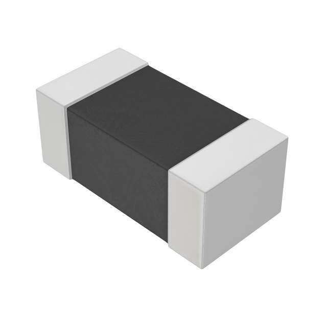
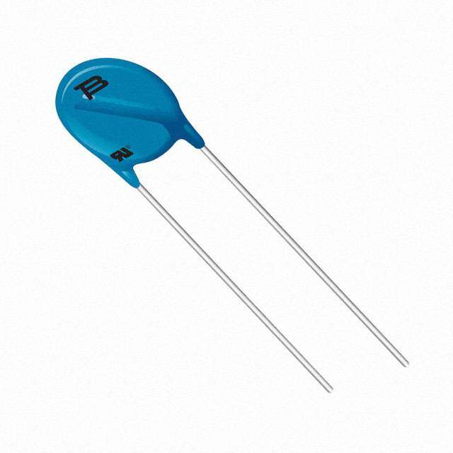
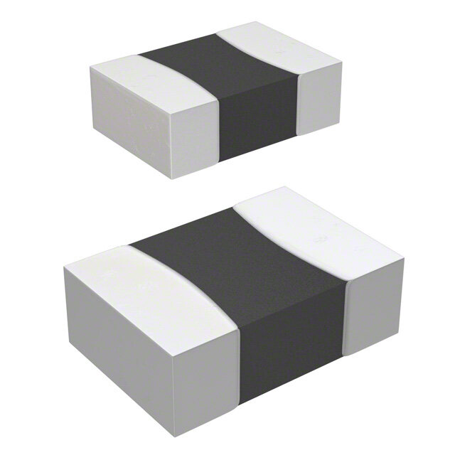
| 产品图片 |
|
| rohs | 符合RoHS无铅 / 符合限制有害物质指令(RoHS)规范要求 |
| 产品系列 | TDK AVRL101A1R1NTAAVRL |
| 数据手册 | |
| 产品型号 | AVRL101A1R1NTA |
| 产品 | MOV |
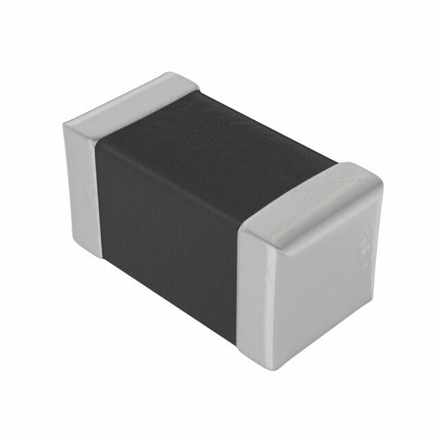
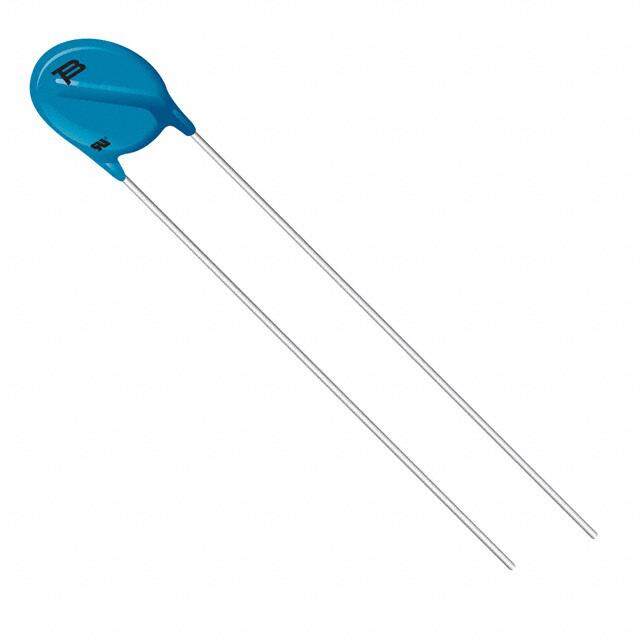
| 产品目录绘图 |
|
| 产品目录页面 | |
| 产品种类 | Varistors |
| 其它名称 | 445-2560-2 |
| 包装 | 带卷 (TR) |
| 变阻器电压 | 90V |
| 商标 | TDK |
| 外壳代码-in | 0402 |
| 外壳代码-mm | 1005 |
| 外壳宽度 | 0.5 mm |
| 安装 | SMD/SMT |
| 宽度 | 0.5 mm |
| 封装 | Reel |
| 封装/外壳 | 0402(1005 公制) |
| 封装/箱体 | 0402 (1005 metric) |
| 尺寸 | 0.5 mm W x 1 mm L x 0.5 mm H |
| 工作温度范围 | - 40 C to + 85 C |
| 工厂包装数量 | 10000 |
| 最大AC电压 | - |
| 最大DC电压 | 10VDC |
| 标准包装 | 10,000 |
| 电压 | 10 VDC |
| 电压额定值DC | 10 V |
| 电容 | 1.1 pF |
| 电流-浪涌 | - |
| 电路数 | 1 |
| 端接类型 | Solder |
| 系列 | AVRL |
| 能量 | - |


- 商务部:美国ITC正式对集成电路等产品启动337调查
- 曝三星4nm工艺存在良率问题 高通将骁龙8 Gen1或转产台积电
- 太阳诱电将投资9.5亿元在常州建新厂生产MLCC 预计2023年完工
- 英特尔发布欧洲新工厂建设计划 深化IDM 2.0 战略
- 台积电先进制程称霸业界 有大客户加持明年业绩稳了
- 达到5530亿美元!SIA预计今年全球半导体销售额将创下新高
- 英特尔拟将自动驾驶子公司Mobileye上市 估值或超500亿美元
- 三星加码芯片和SET,合并消费电子和移动部门,撤换高东真等 CEO
- 三星电子宣布重大人事变动 还合并消费电子和移动部门
- 海关总署:前11个月进口集成电路产品价值2.52万亿元 增长14.8%
PDF Datasheet 数据手册内容提取
VV oo ll tt aa gg ee PP rr oo tt ee cc tt ii oo nn DD ee vv ii cc ee ss FFeebbrruuaarryy 22002200 Cl Pb Br RoHS SRVEHCA-CFrHee HaFlroegeen LFereaed Chip varistors ESD/Voltage protection devices AVR/SGNE series AVRM/AVR-M : Standard Type AVRL : Low Capacitance Type AVRH : High reliability Type SGNE : Low Clamp Type
(2/12) Voltage Protection Devices Chip varistors RoHS Directive Compliant Product Compatible with lead-free solders Overview of the AVR/SGNE series CHARACTERISTICS OF CHIP VARISTOR EQUIVALENT CIRCUIT OF CHIP VARISTORS Varistors are voltage dependent nonlinear resistive elements with 2 Zener Diodes a resistance that decreases rapidly when the voltage is over the constant value. Varistors become zener diode of 2 serial connection and equiva- A capacitance content lent, and does not have polarity. CHIP VARISTORS FEATURE CURRENT vs. VOLTAGE CHARACTERISTICS IEC61000-4-2 LEVEL4 compliant. )A 10–1 Reliability characteristics evaluated based on AEC-Q200 con- (nt 10–2 Zener diode dition. (Automotive products) Curre Positive direction 1100––34 /Vz:6.8V C/Vh1imp Av:a1r2isVtor High ESD withstanding voltage Small-sized products are available 10–5 125°C, 150°C Supported –18 –14 –10 –6 –2 2 6 10 14 18 –10–5 –10–4 Fig.1 Internal structure of multilayer chip varistors –10–3 Negative direction –10–2 –10–1 ① Voltage(V) THE EFFECT OF THE VARISTOR Without varistor A malfunction and failure of electronic equipment ESD, Surge voltage IC Power line ② Signal line ⑤ ③ ④ With Varistor Suppress abnormal voltage by inserting varistor in a circuit No. Name ESD, Surge voltage (1) Semiconductor ceramics (2) Internal electrode(Pd) (3) Ag (4) Terminal electrode Ni Power line IC (5) Sn Signal line Insert a varistor between a line and ground : Chip varistor 20200217 / vpd_varistors_avr_en.fm
(3/12) Voltage Protection Devices Chip varistors RoHS Directive Compliant Product Compatible with lead-free solders Overview of the AVR/SGNE series PART NUMBER CONSTRUCTION AVRM 1608 C 390 K T 271 N L x W Varistor Varistor voltage Capacitance Capacitance Series name dimensions Structure code voltage tolerance Packaging style tolerance (mm) (V) (%) (pF) (%) 0402 0.4x0.2 C General structure 390=39×100 K ±10 T Taping 271=27×101 K ±10 0603 0.6x0.3 6R8 6.8 M ±20 B Bulk 221 220 M ±20 1005 1.0x0.5 270 27 N ±30 271 270 N ±30 1608 1.6x0.8 390 39 2012 2.0×1.2 AVR-M 1608 C 270 M T AAB L x W Varistor Varistor voltage Company Series name dimensions Structure code voltage tolerance Packaging style special symbol (mm) (V) (%) 0603 0.6x0.3 C General structure 270=27×100 K ±10 T Taping 1005 1.0x0.5 G Conductive paste compatible 080 8 M ±20 B Bulk 1608 1.6x0.8 120 12 N ±30 2012 2.0×1.2 270 27 AVRL 10 1A 3R3 F T A L x W Maximum Capacitance Capacitance Company Series name dimensions continuous voltage tolerance Packaging style special symbol (mm) (V) (pF) (pF) 04 0.4x0.2 1A 10 R50 0.5 F ±1 T Taping 06 0.6x0.3 1D 20 1R1 1.1 G ±2 B Bulk 10 1.0×0.5 1E 25 3R3 3.3 N ±0.3 16 1.6×0.8 6R8 6.8 AVRH 10 C 270 K T 150 N A 8 Varistor ESD voltage Operating L x W Varistor Structure voltage Packaging Capacitance Capacitance amount temperature Series name dimensions voltage code tolerance style tolerance IEC61000-4-2 limit (mm) (V) (%) (pF) (kV) (°C) General 1005 1.0x0.5 C 270=27×100 K ±10 T Taping 150=15×100 K ±10% A 25 8 150 structure 270 27 B Bulk 4R7 4.7 M ±20% E 8 390 39 150 15 N ±30% 101 100 500 50 Y ±0.13pF SGNE 04 C 080 M T 150 N 25 Varistor L x W Varistor ESD clamping voltage Structure voltage Packaging Capacitance Capacitance Series name dimensions voltage Average voltage code tolerance style tolerance (IEC61000-4-2, 8kV) (mm) (V) (%) (pF) 04 0.4x0.2 C General structure 080=8×100 K ±10 T Taping 150=15×100 N ±30% 06 0.6x0.3 080 8 B Bulk 6R8 4.7 Y ±0.13pF 10 1.0×0.5 270 27 150 15 L W Shape symbol (JIS) L W T B T 0402 0.40±0.02 0.20±0.02 0.20±0.02 0.07min. 0603 0.60±0.03 0.30±0.03 0.30±0.03 0.1min. 1005 1.00±0.05 0.50±0.05 0.50±0.05 0.1min. 1608 1.60±0.10 0.80±0.10 0.80±0.10 0.2min. B 2012 2.00±0.20 1.25±0.20 0.70±0.20 0.2min. Please be sure to request delivery specifications that provide further details on the features and specifications of the products for proper and safe use. Please note that the contents may change without any prior notice due to reasons such as upgrading. 20200217 / vpd_varistors_avr_en.fm
(4/12) Voltage Protection Devices Chip varistors RoHS Directive Compliant Product Compatible with lead-free solders Overview of the AVR/SGNE series TERMINOLOGY Item Unit Description Varistor voltage V1mA Chip varistor-terminal voltage when DC1mA was flowed (Breakdown voltage) (V) DC voltage that is continuously applied between chip varistor terminals Vdc Terminal chip varistors leakage current-value: 50µA max. Maximum continuous voltage (V) Voltage appearing across the varistor when a pulse current (8/20µs?1) of specified peak value is applied. Vcl Voltage between terminal chip varistors of the Specified peak current value of the impulse current (8/ Clamping voltage (V) 20µs1) is applied E When applied specified peak impulse current-value current (10/1000µs2) once, maximum energy that Maximum energy (Joule) electrical property of chip varistors be not deteriorated Ip When applied impulse current (8/20µs1) once, maximum current that electrical property of chip varis- Maximum peak current (A) tors be not deteriorated C Oscillator frequency 1kHz or 1MHz, capacitance between chip varistor-terminal in oscillator voltage Capacitance (pF) 1Vrms 1 8/20µs test waveform 2 10/1000µs test waveform 100% 100% 90% 90% Current50% Current50% 8µs 10µs 20µs 1000µs Time Time Please be sure to request delivery specifications that provide further details on the features and specifications of the products for proper and safe use. Please note that the contents may change without any prior notice due to reasons such as upgrading. 20200217 / vpd_varistors_avr_en.fm
(5/12) Voltage Protection Devices Chip varistors RoHS Directive Compliant Product Compatible with lead-free solders AVR/SGNE series Product characteristics list PRODUCT CHARACTERISTICS LIST Item V (1mA) C1kHz Vdc Clamping Maximum Maximum Operating IEC61000-4-2 AEC-Q200 *C1MHz voltage energy peak current temperature (Contact) 8/20µs 10/1000µs 8/20µs range (V) (pF) DC (V) Vcl (V) E (J) Ip (A) (°C) 150pF/330 AVRL041E1R1NTA 39(31.2 to 46.8) 1.1(0.8 to 1.4)* 25 — — — –40 to +85 4kV (Level2) AVRM0402C120MT330N 12(9.6 to 14.4) 33(23.1 to 42.9) 5.5 20(1A) 0.005 1 –40 to +85 8kV (Level4) AVRM0402C6R8NT101N 6.8(4.76 to 8.84) 100(70 to 130) 3.5 15(1A) 0.01 4 –40 to +85 8kV (Level4) SGNE04C080MT150N25 8(6.4 to 9.6) 15(10.5 to 19.5) 5.5 21(1A) 0.005 1 –40 to +85 8kV (Level4) AVRL061E1R1NTA 39(35.0 to 43.0) 1.1(0.8 to 1.4)* 25 — — — –40 to +85 4kV (Level2) AVRL061FR50ETA 140(112 to 168) 0.5(0.3 to 0.7)* 30 — — — –40 to +85 4kV (Level2) AVRM0603C080MT101N 8(6.4 to 9.6) 100(70 to 130) 5.5 17(1A) 0.01 4 –40 to +85 8kV (Level4) AVRM0603C120MT101N 12(9.6 to 14.4) 100(70 to 130) 5.5 20(1A) 0.01 5 –40 to +85 8kV (Level4) AVRM0603C120MT150N 12.8(10.0 to 15.6) 15(10.5 to 19.5) 5.5 35(1A) 0.003 1 –40 to +85 8kV (Level4) AVR-M0603C120MTAAB 12(9.6 to 14.4) 33(23.1 to 42.9) 7.5 23(1A) 0.01 1 –40 to +85 8kV (Level4) AVRM0603C200MT150N 20(16 to 24) 15(10.5 to 19.5)* 12 40(1A) 0.01 1 –40 to +85 8kV (Level4) AVRM0603C6R8NT101N 6.8(4.76 to 8.84) 100(70 to 130) 3.5 14(1A) 0.01 10 –40 to +85 8kV (Level4) AVRM0603C6R8NT331N 6.8(4.76 to 8.84) 330(231 to 429) 3.5 14(1A) 0.02 16 –40 to +85 8kV (Level4) SGNE06C080MT150N25 8(6.4 to 9.6) 15(10.5 to 19.5) 5.5 21(1A) 0.005 1 –40 to +85 8kV (Level4) SGNE06C270MT6R8G60 27(21.6 to 32.4) 6.8(4.8 to 8.8)* 15 54(1A) 0.005 1 –40 to +85 8kV (Level4) AVRL101A1R1NTA 90(79.6 to 110.4) 1.1(0.8 to 1.4)* 10 — — — –40 to +85 8kV (Level4) AVRL101E1R1NTB 39(31.2 to 46.8) 1.1(0.8 to 1.4)* 25 — — — –40 to +85 4kV (Level2) AVRL101D3R3FTA 27(21.6 to 32.4) 3.3(2.3 to 4.3)* 20 62(0.5A) 0.01 0.5 –40 to +125 8kV (Level4) ✔ AVRL101D6R8GTA 27(21.6 to 32.4) 6.8(4.8 to 8.8)* 20 58(1A) 0.01 1 –40 to +125 8kV (Level4) ✔ AVR-M1005C080MTAAB 8(6.4 to 9.6) 650(520 to 780) 5.5 14(1A) 0.04 25 –40 to +85 8kV (Level4) AVR-M1005C080MTABB 8(6.4 to 9.6) 100(55 to 145) 5.5 15(1A) 0.02 3 –40 to +85 8kV (Level4) AVR-M1005C080MTACB 8(6.4 to 9.6) 33(14 to 52) 5.5 19(1A) 0.01 1 –40 to +85 8kV (Level4) AVR-M1005C080MTADB 8(6.4 to 9.6) 480(384 to 576) 5.5 14(1A) 0.04 25 –40 to +85 8kV (Level4) AVR-M1005C120MTAAB 12(9.6 to 14.4) 130(104 to 156) 7.5 20(1A) 0.05 10 –40 to +85 8kV (Level4) AVR-M1005C120MTACC 12(9.6 to 14.4) 460(276 to 644)* 7.5 21(1A) 0.01 24 –40 to +85 8kV (Level4) AVR-M1005C180MTAAB 18(14.4 to 21.6) 120(72 to 168)* 11 30(1A) 0.06 16 –40 to +85 8kV (Level4) AVRM1005C270KT101N 27(24.0 to 30.0) 100(70 to 130) 19 44(1A) 0.06 4 –40 to +85 8kV (Level4) AVR-M1005C270MTAAB 27(21.6 to 32.4) 40(30 to 48) 15 47(1A) 0.04 47 –40 to +85 8kV (Level4) AVR-M1005C270MTABB 27(21.6 to 32.4) 15(10.5 to 19.5) 15 49(1A) 0.05 1 –40 to +85 8kV (Level4) AVRM1005C6R8NT101N 6.8(4.76 to 8.84) 100(70 to 130) 3.5 14(1A) 0.02 10 –40 to +85 8kV (Level4) AVRM1005C6R8NT331N 6.8(4.76 to 8.84) 330(231 to 429) 3.5 15(1A) 0.008 24 –40 to +85 8kV (Level4) SGNE10C080MT150N28 8(6.4 to 9.6) 15(10.5 to 19.5) 5.5 21V(1A) 0.01 19 –40 to +85 8kV (Level4) AVRH10C270KT150NA8 27(24.0 to 30.0) 15(10.5 to 19.5) 19 52(2A) 0.02 2 –55 to +150 25kV ✔ AVRH10C270KT350NA8 27(24.0 to 30.0) 35(24.5 to 45.5) 19 52(2A) 0.02 8 –55 to +150 25kV ✔ AVRH10C390KT500NA8 39(35.0 to 43.0) 50(35 to 65) 28 72(2A) 0.02 15 –55 to +150 25kV ✔ AVRH10C101KT4R7FA8 100(90 to 110) 4.7(3.7 to 5.7)* 70 190(1A) 0.03 1 –55 to +150 25kV ✔ AVRH10C101KT1R1NE8 110(100 to 120) 1.1(0.8 to 1.4)* 70 190 (0.3A) 0.01 0.3 –55 to +150 8kV (Level4) ✔ AVRH10C221KT1R5YA8 220 (198 to 242) 1.5(1.37 to 1.63)* 70 400 (0.5A) 0.01 0.5 –55 to +150 25kV AVRL161A1R1NTA 90(79.6 to 110.4) 1.1(0.8 to 1.4)* 10 — — — –40 to +85 8kV (Level4) AVRL161A1R1NTB 39(31.2 to 46.8) 1.1(0.8 to 1.4)* 10 — — — –40 to +85 4kV (Level2) AVRL161D3R3FTA 27(21.6 to 32.4) 3.3(2.3 to 4.3)* 20 62(0.5A) 0.01 0.5 –40 to +125 8kV (Level4) ✔ AVRL161D6R8GTA 27(21.6 to 32.4) 6.8(4.8 to 8.8)* 20 58(1A) 0.01 1 –40 to +125 8kV (Level4) ✔ AVR-M1608C080MTAAB 8(6.4 to 9.6) 650(520 to 780) 5.5 15(2A) 0.09 30 –40 to +85 8kV (Level4) AVR-M1608C120MT2AB 12(9.6 to 14.4) 400(320 to 480) 7.5 20(2A) 0.06 15 –40 to +85 8kV (Level4) AVR-M1608C120MT6AB 12(9.6 to 14.4) 1050(840 to 1260) 7.5 20(2A) 0.09 50 –40 to +85 8kV (Level4) AVR-M1608C180MT6AB 18(14.4 to 21.6) 600(480 to 720) 11 30(2A) 0.10 30 –40 to +85 8kV (Level4) AVR-M1608C220KT2AB 22(19.8 to 24.2) 210(147 to 273) 16 37(2A) 0.03 10 –40 to +125 25kV ✔ AVR-M1608C220KT6AB 22(19.8 to 24.2) 560(392 to 728) 16 34(2A) 0.10 30 –40 to +125 25kV ✔ AVR-M1608C270MTABB 27(21.6 to 32.4) 15(10.5 to 19.5) 17 52(2A) 0.05 2 –55 to +150 25kV ✔ AVR-M1608C270MTAAB 27(21.6 to 32.4) 30(21 to 39) 17 52(2A) 0.05 2 –55 to +150 25kV ✔ AVR-M1608C270KTACB 27(24.0 to 30.0) 60(42 to 78) 19 54(2A) 0.05 10 –55 to +150 25kV ✔ AVRM1608C270KT800M 27(24.0 to 30.0) 80(64 to 96) 19 53(2A) 0.02 28 –55 to +150 25kV ✔ AVR-M1608C270KT2AB 27(24.0 to 30.0) 160(112 to 208) 19 42(2A) 0.10 20 –55 to +150 25kV ✔ AVRM1608C270KT221M 27(24.0 to 30.0) 220(176 to 264) 19 52(2A) 0.10 40 –55 to +150 25kV ✔ AVR-M1608C270KT6AB 27(24.0 to 30.0) 430(301 to 559) 19 42(2A) 0.10 48 –55 to +150 25kV ✔ AVR-M1608G270KT6AB 27(24.0 to 30.0) 430(301 to 559) 19 42(2A) 0.10 48 –55 to +150 25kV ✔ AVRM1608C390KT271N 39(35.0 to 43.0) 270(189 to 351) 28 69(2A) 0.10 78 –55 to +150 25kV ✔ AVRM1608C560KT101M 56(50.4 to 61.6) 100(80 to 120) 40 113(2A) 0.10 60 –55 to +150 25kV ✔ AVRM1608C720KT750M 72(64.8 to 79.2) 75(60 to 90) 53 135(2A) 0.10 40 –55 to +150 25kV ✔ AVR-M2012C120MT6AB 12(9.6 to 14.4) 1000(550 to 1450) 7.5 20(5A) 0.20 60 –40 to +85 8kV (Level4) AVR-M2012C220KT6AB 22(19.8 to 24.2) 800(560 to 1040) 16 38(5A) 0.30 100 –40 to +125 25kV ✔ AVRM2012C330KT801N 33(29.7 to 36.3) 800(560 to 1040) 24 59(5A) 0.50 240 –55 to +150 25kV ✔ AVR-M2012C390KT6AB 39(35.0 to 43.0) 430(387 to 483) 28 62(5A) 0.30 100 –55 to +150 25kV ✔ AVRM2012C560KT251M 56(50.4 to 61.6) 250(200 to 300) 40 113(5A) 0.30 150 –55 to +150 25kV ✔ AVRM2012C720KT201M 72(64.8 to 79.2) 200(160 to 240) 53 142(5A) 0.30 100 –55 to +150 25kV ✔ Please be sure to request delivery specifications that provide further details on the features and specifications of the products for proper and safe use. Please note that the contents may change without any prior notice due to reasons such as upgrading. 20200217 / vpd_varistors_avr_en.fm
(6/12) Voltage Protection Devices Chip varistors RoHS Directive Compliant Product Compatible with lead-free solders AVR/SGNE series Electrostatic absorption characteristics DISCHARGE VOLTAGE WAVEFORM (EXAMPLE) WITHOUT VARISTOR, WAVEFORM AT VARISTOR INSTALLATION WAVEFORM AT VARISTOR INSTALLATION 1800 180 1600 160 Without Varistor 1400 140 1200 120 )V1000 )V100 AVRH10C270KT150NA8 (e AVRH10C270KT150NA8 (e AVR-M1608C270KT6AB g 800 g 80 olta 600 AVR-M1608C270KT6AB olta 60 V AVR-M1608C220KT6AB V 400 40 200 20 AVR-M1608C220KT6AB 0 0 –200 –20 –50 0 50 100 150 200 250 300 –50 0 50 100 150 200 250 300 Time(ns) Time(ns) Test conditions 150pF/330 (IEC61000-4-2) Contact discharge, Charged voltage 8kV TEST CIRCUIT DIAGRAM Discharge gun Test sample 60dB attenuator 50Ω ESD simulator Oscilloscope I/O impedance: 50Ω Shield Discharge SMA Point Connector PCB ESD Simulator Chip Coaxial Attenuator(60dB) Oscilloscope Varistor Cable 50Ω 50Ω Please be sure to request delivery specifications that provide further details on the features and specifications of the products for proper and safe use. Please note that the contents may change without any prior notice due to reasons such as upgrading. 20200217 / vpd_varistors_avr_en.fm
(7/12) Voltage Protection Devices Chip varistors RoHS Directive Compliant Product Compatible with lead-free solders Attention on a circuit board design Board design (2) When peak levels panning-at soldering is excessive, by solder contraction stress, mechanical-thermal stress causes a Yasuku When attached to chip varistors, amount of silver used (fillet size) chip crack. In addition, when the peak level is underestimated, ter- has direct impact on chip varistors after mounting. Thus, sufficient minal electrode fixed strength is insufficient. This causes chip consideration is necessary. dropouts and may affect circuit reliability. Representative example of the panning of peak levels is shown in the following. Set of land dimensions (1) As the stress rises in the chip varistors owing to the increase in Recommended silver dose silver, breakage and cracks will occur. Cause including crack, as caution on board land design, configure the shape and dimensions Solder stress is increased, Solder volume so that the amount of silver is appropriate. If you installed 2 or and it is easy for a crack to overload form. more parts in the Common Land, separated by a solder resist and special land of each component. Most large serving amount Decent solder Minimum prime amount volume C Fixed strength is weak, and Solder volume there is connection a prob- deficit lem and risk of loss. B A Case and suggested protocol want to avoid Dimensions shape SAymbol B C Example Cases to avoid I(mlanpdro dveivmiseionnt )example 0402 0.20 Nom. 0.15 to 0.21 0.18 to 0.20 Leads Leads 0603 0.25 to 0.35 0.20 to 0.30 0.25 to 0.35 1005 0.30 to 0.50 0.35 to 0.45 0.40 to 0.60 Lead wire and land Chip Solder Solder resist 1608 0.60 to 0.80 0.60 to 0.80 0.60 to 0.80 of part discrete 2012 0.90 to 1.20 0.70 to 0.90 0.90 to 1.20 doubles up PCB Chassis Solder Solder resist (ground solder) Arrangements in the vicinity L1 L2 L2>L1 Land Arrangements of chip component's companion Excess solder Solder resist Land Missing solder Please be sure to request delivery specifications that provide further details on the features and specifications of the products for proper and safe use. Please note that the contents may change without any prior notice due to reasons such as upgrading. 20200217 / vpd_varistors_avr_en.fm
(8/12) Voltage Protection Devices Chip varistors RoHS Directive Compliant Product Compatible with lead-free solders Attention on a circuit board design Arrangements of components (2) In payment near by board, depending on mount position of chip (1) I was based on camber of substrate and suggested protocol of varistors, as mechanical stress varies, please refer to the following chip varistors arrangement, as stress does not join to the utmost is diagram. shown in following. Substrate for flexural stressSubstrate for flexural stress E D Adverse events Good example Perforation C Perforation or slit Perforation or slit B A Direction of surface solder Slit Solder the mountain fold as a Solder the mountain fold as a top. bottom. [Please review the italicized portion, as I am The order of A > B = C > D > E eases the stress. unsure what you mean to con- vey here.] Perforation or slit Perforation or slit Chip arrangements (direction) Mounted vertically to the per- Mounted horizontally to the foration and slit. perforation and slit. L1 L2 Distance from perforation and slit (L1<L2) (L1<L2) portion Close location is disadvanta- It is an advantage so distant geous of perforation and slit. location away places the perfo- ration and slit. Please be sure to request delivery specifications that provide further details on the features and specifications of the products for proper and safe use. Please note that the contents may change without any prior notice due to reasons such as upgrading. 20200217 / vpd_varistors_avr_en.fm
(9/12) Voltage Protection Devices Chip varistors RoHS Directive Compliant Product Compatible with lead-free solders Local precautions Application to board Reflow temperature profile Mounting head pressure Preheating Soldering Natural cooling Under suction nozzle if dead point too, during implementation, Peak excessive force joins of chip varistors low, as cause causes of crack, T4 please use with reference to something about following. e 1) Being set to top surface of substrate so that under suction nozzle ur T3 T3 at as for dead center, substrate does not bend back, and adjust, per m please. Te T2 2) Nozzle pressure at implementation is 0.1 to 0.3N in static load, T: t3 T1 please. 3) Substrate fixes up back surface of substrate with support pin in t1 t2 impact of suction nozzle to wely deflection to the utmost, and substrate hold deflection, please. A representative example is t: Time shown in the following. Specification Cases to avoid Recommended case Item For eutectic mixture Use of lead-free solder solder Crack Preheating temperature 160 to 180°C 150 to 180°C Single-sided Solder melting temperature 200°C 230°C mounting Maximum temperature 240°C max. 260°C max. Preheating time 100s max. 120s max. Support pin Time to reach higher than the 30s max. 40s max. solder melting temperature number of possible reflow cycles 2 max. 2 max. Double-sided mounting Soldering iron Solder peeling Crack Support pin The tip temperature and also by (1) types of soldering irons, the size of the substrate, and the geometry of the land pattern. Being earlier, Mechanical shock that, if positioning your nail to wear, ragged edge but when as there is possibility that crack occurs in the heat ander- of positionings, participates in chip varistors are locally, and chip son impaction, point soldering iron temperature is high, please do varistors, as there is possibility of crack generated, cut the closed solder work within the following conditions. positioning, and maintenance and inspection, and, exchange of Temperature Wattage Pallet point Soldering time of iron tips Frequency manage dimensions and position nail periodically, please. (W) shape (mm) (Second) (°C) Within each Soldering terminal once 350max. 30max. ø3.0max. 5 max. (Within total of Significant impact is possible on the performance of chip varistors, twice) flux checks something about follow, please use. (1) Flux uses one with 0.1wt % (Cl conversion) or less halide sub- Direct iron tip is in contact with the (2) chip varistors body, and the stance contains amounts, please. In addition, do not do this with strain owing to thermal shock in particular grows even if a crack is strongly acidic objects. generated. Therefore, please do not touch it directly to the terminal Flux during is soldered (2) Chip varistors is applied the smalleset electrodes. amount necessary, please. (3) If Used soluble flux, perform thorough wash particularly, please. Please be sure to request delivery specifications that provide further details on the features and specifications of the products for proper and safe use. Please note that the contents may change without any prior notice due to reasons such as upgrading. 20200217 / vpd_varistors_avr_en.fm
(10/12) Voltage Protection Devices Chip varistors RoHS Directive Compliant Product Compatible with lead-free solders Attention after implementation Cleaning (2) During each substrate operational check, push pressure with contact failure of check pin of boards checkers of check pin may be (1) If cleaning liquid is inappropriate, residues and other foreign toned up to be prevented. As substrate is bent under loading, chip body of fluxes builds up on chip varistors, and can degrade the per- varistors is broken owing to stress. There is also the possibility that formance of chip varistors (particularly the insulation resistance). solder on the terminal electrode will peel off. Follow the diagram for (2) Wash conditions may compromise performance of chip varistors reference, and check that the substrate bends, please. if they are improper (wash due, wash excess). 2-1) For wash due Item Cases to avoid Recommended case (a) By substance of a system in flux residue halide, metal including Peeling Support pin terminal electrodes may experience corrosion. Substrate sags (b) Substance of a system in flux residue halide builds up on chip Check pin Check pin varistors, and reduces the insulation resistance. (c) Soluble flux makes comparisons of colophony series flux, and there is event with trends of significant (1) and(2). Single-part component handling 2-2) For excess wash To drop impact, as there is possibility that breakage and crack is (1) Owing to lavage, chip varistors deteriorates, and reduces perfor- entered, do not chip varistors that(1) chip varistors falls. mance of chip varistors. (2) In ultrasonography, when output is passed, substrate resonates size, and crack occurs in body and sprang of chip varistors in Crack vibration of substrate. Since this may reduce the strength of the terminal electrode, please note the following conditions. [Please review the italicized portion, as I am unsure what you mean to Floor convey here.] (2) At stacking storage after implementation and treatment of sub- Ultrasound output strate, corner of boards is regarded as chip varistors. Please be Ultrasonic frequency careful, as there is the possibility that breakage and cracks will Ultrasound cleaning time occur on impact. 2-3) Concentration including halogen that when cleaning liquid to pollution, when you released is higher, and may cause similar of Crack Board results into wash due. Substrate handling after component mounting (1) When substrate is divided, a flexible so that show in following dia- gram to substrate, and is given by stress including twist, as there is possibility that crack occurs of chip varistors, please check that stress is within acceptable limits. Bends Twist Please be sure to request delivery specifications that provide further details on the features and specifications of the products for proper and safe use. Please note that the contents may change without any prior notice due to reasons such as upgrading. 20200217 / vpd_varistors_avr_en.fm
(11/12) Voltage Protection Devices Chip varistors RoHS Directive Compliant Product Compatible with lead-free solders Packaging style REEL DIMENSIONS PACKAGE QUANTITY / INDIVIDUAL WEIGHT Package quantity Individual weight 2.0±0.5 Type (pieces/reel) (mg) AVRM0402/AVRL04/SNGE04 20,000 0.1 AVRM0603/AVR-M0603/AVRL06/ 15,000 0.2 SGNE06 AVRM1005/AVR-M1005/AVRL10/ 10,000 1.2 AVRH10 n. AVRM1608/AVR-M1608/AVRL16 4,000 5 mi AVRM2012/AVR-M2012 2,000 13 0 6 ø 0.8 ø13±0.2 9.0max. ø21±0.8 14.0max. ø180±2.0 Dimensions in mm TAPE DIMENSIONS 1 0. 1.5+00.1 2.0±0.05 4.0±0.1 75± 1. 5 0 ±0. 0.3 5 ± B 3. 8.0 A P1 T Dimensions in mm Type A B P1 T 0402 0.26±0.04 0.46±0.04 2.0±0.05 0.40max. 0603 0.38±0.05 0.68±0.05 2.0±0.05 0.45max. 1005 0.65+0.05/–0.1 1.15+0.05/–0.1 2.0±0.05 0.65max. 1608 1.1±0.2 1.9±0.2 4.0±0.1 1.1max. 2012 1.5±0.2 2.3±0.2 4.0±0.1 1.1max 160min. Taping 200min. Drawing direction 300min. Dimensions in mm Please be sure to request delivery specifications that provide further details on the features and specifications of the products for proper and safe use. Please note that the contents may change without any prior notice due to reasons such as upgrading. 20200217 / vpd_varistors_avr_en.fm
(12/12) Voltage Protection Devices REMINDERS FOR USING THESE PRODUCTS Before using these products, be sure to request the delivery specifications. SAFETY REMINDERS Please pay sufficient attention to the warnings for safe designing when using this products. REMINDERS Please pay careful attention to the precautions and follow safe designing practices when using these products. Please observe the following precautions in order to avoid problems with chip varistors such as characteristic degradation and element destruction Please store these products in an environment with a temperature of 5 to 40°C and humidity level of 20 to 70%RH, and use them within six months. Poor storage conditions may lead to the deterioration of the solderability of the edge electrodes, so please be careful to avoid contact with humidity, dew condensation, dust, toxic gas (hydrogen, hydrogen sulfide, sulfurous acid, chlorine, ammonia, etc.), direct sunlight, and so on. Please do not use products that have been dropped or detached when mounting. Please solder with the reflow soldering method, and not the flow (dip) soldering method. Please observe the following precautions to avoid problems with varistors such as characteristic degradation and element destruction, which ultimately lead to the generation of heat and smoke with the elements. Do not use in locations where the temperatures exceed the operating temperature range such as under direct sunlight or near sources of heat. Do not use in locations where there are high levels of humidity such as under direct exposure to weather and areas where steam is released. Do not use in locations such as dusty areas, high-saline environments, places where the atmosphere is contaminated with corrosive gas, etc. Avoid powerful vibrations, impact (such as by dropping), pressure, etc. that may lead to splitting in the products. Do not use with a voltage that exceeds the maximum allowable circuit voltage. When resin coating (including modular) a varistor, do not use a resin that will cause deterioration of the varistor. Be sure never to use resin that generates hydrogen as palladium is used for the inner electrode. Avoid attachment near combustible materials. Please contact our sales offices when considering the use of the products listed on this catalog for applications, whose performance and/or quality require a more stringent level of safety or reliability, or whose failure, malfunction or trouble could cause serious damage to society, person or property ('specific uses' such as automobiles, airplanes,medical instruments, nuclear devices, etc.) as well as when considering the use for applications that exceed the range and conditions of this catalog. Please also contact us when using these products for automotive applications. As range of catalog, conditions are transcended, or for damage that generated by was used in application specific, etc, accept no the responsibility, wish. Please take appropriate measures such as acquiring protective circuits and devices that meet the uses, applications, and conditions of the instruments and keeping backup circuits. Please be sure to request delivery specifications that provide further details on the features and specifications of the products for proper and safe use. Please note that the contents may change without any prior notice due to reasons such as upgrading. 20200217 / vpd_varistors_avr_en.fm