ICGOO在线商城 > 集成电路(IC) > 嵌入式 - 微控制器 > ATTINY40-MMHR
 Datasheet下载
- 型号: ATTINY40-MMHR
- 制造商: Atmel
- 库位|库存: xxxx|xxxx
- 要求:
| 数量阶梯 | 香港交货 | 国内含税 |
| +xxxx | $xxxx | ¥xxxx |
查看当月历史价格
查看今年历史价格
ATTINY40-MMHR产品简介:
ICGOO电子元器件商城为您提供ATTINY40-MMHR由Atmel设计生产,在icgoo商城现货销售,并且可以通过原厂、代理商等渠道进行代购。 ATTINY40-MMHR价格参考¥5.66-¥6.40。AtmelATTINY40-MMHR封装/规格:嵌入式 - 微控制器, AVR 微控制器 IC AVR® ATtiny 8-位 12MHz 4KB(2K x 16) 闪存 20-VQFN(3x3)。您可以下载ATTINY40-MMHR参考资料、Datasheet数据手册功能说明书,资料中有ATTINY40-MMHR 详细功能的应用电路图电压和使用方法及教程。
ATTINY40-MMHR 是 Microchip Technology 公司推出的低功耗 8 位 AVR 微控制器,属于嵌入式微控制器类别。其应用场景广泛,特别适合对功耗敏感、需要高集成度和小型化设计的电子产品。以下是该型号的主要应用场景:

1. 电池供电设备
   ATTINY40-MMHR 的低功耗特性使其非常适合电池供电的设备,如无线传感器节点、智能家居设备(如温湿度传感器、烟雾报警器)以及便携式医疗设备(如血糖仪、脉搏血氧仪)。它可以在休眠模式下进一步降低功耗,延长电池寿命。

2. 物联网 (IoT) 设备
   作为一款嵌入式微控制器,ATTINY40-MMHR 可用于 IoT 边缘节点设备中,例如环境监测系统、农业自动化中的土壤湿度检测器等。其片上外设(如 ADC、DAC 和串行通信接口)支持数据采集和传输功能。

3. 消费类电子产品
   在消费电子领域,它可以应用于遥控器、玩具、键盘和鼠标等外设中。这些产品通常要求低成本、小尺寸和低功耗,而 ATTINY40-MMHR 恰好满足这些需求。

4. 工业控制
   在工业环境中,ATTINY40-MMHR 可用作小型控制器或辅助处理器,执行简单的任务,比如电机控制、LED 驱动或开关状态监控。它的 PWM 功能有助于实现精确的速度调节。

5. 音频与灯光控制
   由于具备 DAC 和可编程外设,ATTINY40-MMHR 能够生成波形信号,适用于音效生成或灯光效果控制,例如音乐播放器的音量调节电路或 RGB 灯光控制系统。

6. 汽车电子
   在汽车应用中,它可以用于车内环境监测(如温度、湿度)、座椅加热控制或简单的车载娱乐系统功能扩展。

7. 教育与开发平台
   凭借其易用性和丰富的开发资源,ATTINY40-MMHR 常被用作教学工具或开发者原型设计的核心组件,帮助学生和工程师快速构建项目。

综上所述,ATTINY40-MMHR 凭借其低功耗、高性能和灵活的外设配置,在多种嵌入式应用场景中表现出色,是许多小型化、智能化产品的理想选择。
| 参数 | 数值 |
| 产品目录 | 集成电路 (IC) |
| 描述 | IC MCU 8BIT 4KB FLASH 20VQFN |
| EEPROM容量 | - |
| 产品分类 | |
| I/O数 | 18 |
| 品牌 | Atmel |
| 数据手册 | |
| 产品图片 |
|
| 产品型号 | ATTINY40-MMHR |
| PCN其它 | |
| PCN设计/规格 | |
| RAM容量 | 256 x 8 |
| rohs | 无铅 / 符合限制有害物质指令(RoHS)规范要求 |
| 产品系列 | AVR® ATtiny |
| 产品培训模块 | http://www.digikey.cn/PTM/IndividualPTM.page?site=cn&lang=zhs&ptm=25784http://www.digikey.cn/PTM/IndividualPTM.page?site=cn&lang=zhs&ptm=26162http://www.digikey.cn/PTM/IndividualPTM.page?site=cn&lang=zhs&ptm=26159http://www.digikey.cn/PTM/IndividualPTM.page?site=cn&lang=zhs&ptm=26180 |
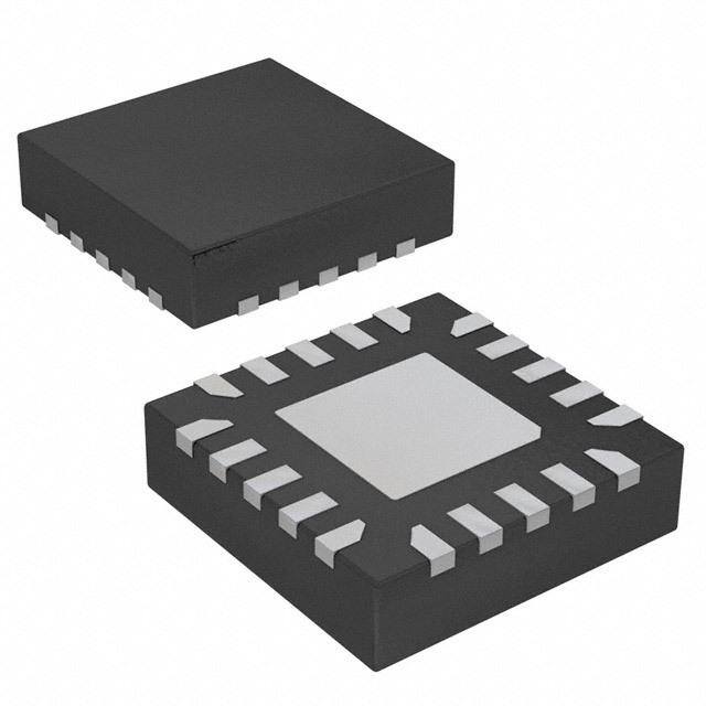
| 供应商器件封装 | 20-VQFN(3x3) |
| 其它名称 | ATTINY40-MMHRCT |
| 包装 | 剪切带 (CT) |
| 外设 | 欠压检测/复位,POR,PWM,WDT |
| 封装/外壳 | 20-VFQFN 裸露焊盘 |
| 工作温度 | -40°C ~ 85°C |
| 振荡器类型 | 内部 |
| 数据转换器 | A/D 12x10b |
| 标准包装 | 1 |
| 核心处理器 | AVR |
| 核心尺寸 | 8-位 |
| 电压-电源(Vcc/Vdd) | 1.8 V ~ 5.5 V |
| 程序存储器类型 | 闪存 |
| 程序存储容量 | 4KB(2K x 16) |
| 连接性 | I²C, SPI |
| 速度 | 12MHz |


- 商务部:美国ITC正式对集成电路等产品启动337调查
- 曝三星4nm工艺存在良率问题 高通将骁龙8 Gen1或转产台积电
- 太阳诱电将投资9.5亿元在常州建新厂生产MLCC 预计2023年完工
- 英特尔发布欧洲新工厂建设计划 深化IDM 2.0 战略
- 台积电先进制程称霸业界 有大客户加持明年业绩稳了
- 达到5530亿美元!SIA预计今年全球半导体销售额将创下新高
- 英特尔拟将自动驾驶子公司Mobileye上市 估值或超500亿美元
- 三星加码芯片和SET,合并消费电子和移动部门,撤换高东真等 CEO
- 三星电子宣布重大人事变动 还合并消费电子和移动部门
- 海关总署:前11个月进口集成电路产品价值2.52万亿元 增长14.8%


PDF Datasheet 数据手册内容提取
8-bit Atmel tinyAVR Microcontroller with 4K Bytes In-System Programmable Flash ATtiny40 Features • High Performance, Low Power AVR® 8-Bit Microcontroller (cid:129) Advanced RISC Architecture – 54 Powerful Instructions – Most Single Clock Cycle Execution – 16 x 8 General Purpose Working Registers – Fully Static Operation – Up to 12 MIPS Throughput at 12 MHz (cid:129) Non-volatile Program and Data Memories – 4K Bytes of In-System Programmable Flash Program Memory – 256 Bytes Internal SRAM – Flash Write/Erase Cycles: 10,000 – Data Retention: 20 Years at 85oC / 100 Years at 25oC (cid:129) Peripheral Features – One 8-bit Timer/Counter with Two PWM Channels – One 8/16-bit Timer/Counter – 10-bit Analog to Digital Converter (cid:129) 12 Single-Ended Channels – Programmable Watchdog Timer with Separate On-chip Oscillator – On-chip Analog Comparator – Master/Slave SPI Serial Interface – Slave TWI Serial Interface (cid:129) Special Microcontroller Features – In-System Programmable – External and Internal Interrupt Sources – Low Power Idle, ADC Noise Reduction, Stand-by and Power-down Modes – Enhanced Power-on Reset Circuit – Internal Calibrated Oscillator (cid:129) I/O and Packages – 20-pin SOIC: 18 Programmable I/O Lines – 20-pin TSSOP: 18 Programmable I/O Lines – 20-pad VQFN: 18 Programmable I/O Lines (cid:129) Operating Voltage: – 1.8 – 5.5V (cid:129) Programming Voltage: – 5V (cid:129) Speed Grade – 0 – 4 MHz @ 1.8 – 5.5V – 0 – 8 MHz @ 2.7 – 5.5V – 0 – 12 MHz @ 4.5 – 5.5V (cid:129) Industrial Temperature Range (cid:129) Low Power Consumption – Active Mode: (cid:129) 200 µA at 1 MHz and 1.8V – Idle Mode: (cid:129) 25 µA at 1 MHz and 1.8V – Power-down Mode: (cid:129) < 0.1 µA at 1.8V 8263B–AVR–01/2013
1. Pin Configurations Figure 1-1. Pinout of ATtiny40 SOIC/TSSOP (PCINT8/ADC8) PB0 1 20 PB1 (ADC9/PCINT9) (PCINT7/ADC7) PA7 2 19 PB2 (ADC10/PCINT10) (PCINT6/ADC6) PA6 3 18 PB3 (ADC11/PCINT11) (PCINT5/ADC5/OC0B) PA5 4 17 PC0 (OC0A/SS/PCINT12) (PCINT4/ADC4/T0) PA4 5 16 PC1 (SCK/SCL/ICP1/T1/PCINT13) (PCINT3/ADC3) PA3 6 15 PC2 (INT0/CLKO/MISO/PCINT14) (PCINT2/ADC2/AIN1) PA2 7 14 PC3 (RESET/PCINT15) (PCINT1/ADC1/AIN0) PA1 8 13 PC4 (MOSI/SDA/TPIDATA/PCINT16) (PCINT0/ADC0) PA0 9 12 PC5 (CLKI/TPICLK/PCINT17) GND 10 11 VCC VQFN 0) 1) 7) 8) 9) T1 T1 T T T N N CIN CIN CIN PCI PCI 7/P 8/P 9/P 10/ 11/ C C C C C D D D D D A A A A A 7 ( 0 ( 1 ( 2 ( 3 ( A B B B B P P P P P 0 9 8 7 6 2 1 1 1 1 (PCINT6/ADC6) PA6 1 15 PC0 (OC0A/SS/PCINT12) (PCINT5/ADC5/OC0B) PA5 2 14 PC1 (SCK/SCL/ICP1/T1/PCINT13) (PCINT4/ADC4/T0) PA4 3 13 PC2 (INT0/CLKO/MISO/PCINT14) (PCINT3/ADC3) PA3 4 12 PC3 (RESET/PCINT15) (PCINT2/ADC2/AIN1) PA2 5 11 PC4 (MOSI/SDA/TPIDATA/PCINT16) 0 6 7 8 9 1 1 0 D C 5 A A N C C 0) P 0) P G V K) P N C L AI D C C1/ 0/A TPI 1/AD CINT CLKI/ CINT (P T17/ P N ( CI P ( NOTE: Bottom pad should be soldered to ground. ATtiny40 [DATASHEET] 2 8263B–AVR–01/2013
1.1 Pin Description 1.1.1 VCC Supply voltage. 1.1.2 GND Ground. 1.1.3 RESET Reset input. A low level on this pin for longer than the minimum pulse length will generate a reset, even if the clock is not running and provided the reset pin has not been disabled. The minimum pulse length is given in Table 20-4 on page 155. Shorter pulses are not guaranteed to generate a reset. The reset pin can also be used as a (weak) I/O pin. 1.1.4 Port A (PA7:PA0) Port A is a 8-bit bi-directional I/O port with internal pull-up resistors (selected for each bit). The Port A output buffers have symmetrical drive characteristics with both high sink and source capability. As inputs, Port A pins that are externally pulled low will source current if the pull-up resistors are activated. The Port A pins are tri-stated when a reset condition becomes active, even if the clock is not running. Port A has alternate functions as analog inputs for the ADC, analog comparator and pin change interrupt as described in “Alternate Port Functions” on page 47. 1.1.5 Port B (PB3:PB0) Port B is a 4-bit bi-directional I/O port with internal pull-up resistors (selected for each bit). The Port B output buffers have symmetrical drive characteristics with both high sink and source capability. As inputs, Port B pins that are externally pulled low will source current if the pull-up resistors are activated. The Port B pins are tri-stated when a reset condition becomes active, even if the clock is not running. The port also serves the functions of various special features of the ATtiny40, as listed on page 37. 1.1.6 Port C (PC5:PC0) Port C is a 6-bit bi-directional I/O port with internal pull-up resistors (selected for each bit). The Port C output buf- fers have symmetrical drive characteristics with both high sink and source capability except PC3 which has the RESET capability. To use pin PC3 as an I/O pin, instead of RESET pin, program (‘0’) RSTDISBL fuse. As inputs, Port C pins that are externally pulled low will source current if the pull-up resistors are activated. The Port C pins are tri-stated when a reset condition becomes active, even if the clock is not running. Port C has alternate functions as analog inputs for the ADC, analog comparator and pin change interrupt as described in “Alternate Port Functions” on page 47. The port also serves the functions of various special features of the ATtiny40, as listed on page 37. 2. Overview ATtiny40 is a low-power CMOS 8-bit microcontroller based on the compact AVR enhanced RISC architecture. By executing powerful instructions in a single clock cycle, the ATtiny40 achieves throughputs approaching 1 MIPS per MHz allowing the system designer to optimize power consumption versus processing speed. Figure 2-1. Block Diagram The AVR core combines a rich instruction set with 16 general purpose working registers and system registers. All registers are directly connected to the Arithmetic Logic Unit (ALU), allowing two independent registers to be ATtiny40 [DATASHEET] 3 8263B–AVR–01/2013
VCC RESET PROGRAMMING PROGRAM INTERNAL CALIBRATED LOGIC COUNTER OSCILLATOR OSCILLATOR PROGRAM STACK WATCHDOG TIMING AND FLASH POINTER TIMER CONTROL INSTRUCTION RESET FLAG REGISTER SRAM REGISTER INSTRUCTION INTERRUPT MCU STATUS DECODER UNIT REGISTER CONTROL GENERAL TIMER/ LINES PURPOSE COUNTER0 REGISTERS X Y Z TIMER/ COUNTER1 ALU SPI ANALOG COMPARATOR ISP STATUS INTERFACE REGISTER TWI ADC 8-BIT DATA BUS DATA REGISTER DIRECTION DATA REGISTER DIRECTION DATA REGISTER DIRECTION PORT A REG. PORT A PORT B REG. PORT B PORT C REG. PORT C DRIVERS DRIVERS DRIVERS PORT A PORT B PORT C PA[7:0] PB[3:0] PC[5:0] GND accessed in one single instruction executed in one clock cycle. The resulting architecture is compact and code effi- cient while achieving throughputs up to ten times faster than conventional CISC microcontrollers. The ATtiny40 provides the following features: 4K bytes of In-System Programmable Flash, 256 bytes of SRAM, twelve general purpose I/O lines, 16 general purpose working registers, an 8-bit Timer/Counter with two PWM channels, a 8/16-bit Timer/Counter, Internal and External Interrupts, an eight-channel, 10-bit ADC, a programma- ble Watchdog Timer with internal oscillator, a slave two-wire interface, a master/slave serial peripheral interface, an internal calibrated oscillator, and four software selectable power saving modes. Idle mode stops the CPU while allowing the Timer/Counter, ADC, Analog Comparator, SPI, TWI, and interrupt sys- tem to continue functioning. ADC Noise Reduction mode minimizes switching noise during ADC conversions by stopping the CPU and all I/O modules except the ADC. In Power-down mode registers keep their contents and all chip functions are disabled until the next interrupt or hardware reset. In Standby mode, the oscillator is running while the rest of the device is sleeping, allowing very fast start-up combined with low power consumption. ATtiny40 [DATASHEET] 4 8263B–AVR–01/2013
The device is manufactured using Atmel’s high density non-volatile memory technology. The on-chip, in-system programmable Flash allows program memory to be re-programmed in-system by a conventional, non-volatile memory programmer. The ATtiny40 AVR is supported by a suite of program and system development tools, including macro assemblers and evaluation kits. 3. General Information 3.1 Resources A comprehensive set of drivers, application notes, data sheets and descriptions on development tools are available for download at http://www.atmel.com/avr. 3.2 Code Examples This documentation contains simple code examples that briefly show how to use various parts of the device. These code examples assume that the part specific header file is included before compilation. Be aware that not all C compiler vendors include bit definitions in the header files and interrupt handling in C is compiler dependent. Please confirm with the C compiler documentation for more details. 3.3 Capacitive Touch Sensing Atmel QTouch Library provides a simple to use solution for touch sensitive interfaces on Atmel AVR microcon- trollers. The QTouch Library includes support for QTouch® and QMatrix® acquisition methods. Touch sensing is easily added to any application by linking the QTouch Library and using the Application Program- ming Interface (API) of the library to define the touch channels and sensors. The application then calls the API to retrieve channel information and determine the state of the touch sensor. The QTouch Library is free and can be downloaded from the Atmel website. For more information and details of implementation, refer to the QTouch Library User Guide – also available from the Atmel website. 3.4 Data Retention Reliability Qualification results show that the projected data retention failure rate is much less than 1 PPM over 20 years at 85°C or 100 years at 25°C. 3.5 Disclaimer Typical values contained in this datasheet are based on simulations and characterization of other AVR microcon- trollers manufactured on the same process technology. 4. CPU Core This section discusses the AVR core architecture in general. The main function of the CPU core is to ensure cor- rect program execution. The CPU must therefore be able to access memories, perform calculations, control peripherals, and handle interrupts. ATtiny40 [DATASHEET] 5 8263B–AVR–01/2013
4.1 Architectural Overview Figure 4-1. Block Diagram of the AVR Architecture Data Bus 8-bit Program Status Interrupt Flash Counter and Control Unit Program Memory Watchdog Timer 16 x 8 Instruction General Register Purpose Analog Registrers Comparator Instruction Decoder ADC g g n n si ssi es ALU Control Lines dre ddr Timer/Counter 0 d A ct A ect Dire ndir Timer/Counter 1 I Data SPI SRAM TWI Slave I/O Lines In order to maximize performance and parallelism, the AVR uses a Harvard architecture – with separate memories and buses for program and data. Instructions in the program memory are executed with a single level pipelining. While one instruction is being executed, the next instruction is pre-fetched from the program memory. This concept enables instructions to be executed in every clock cycle. The program memory is In-System Reprogrammable Flash memory. The fast-access Register File contains 16 x 8-bit general purpose working registers with a single clock cycle access time. This allows single-cycle Arithmetic Logic Unit (ALU) operation. In a typical ALU operation, two oper- ands are output from the Register File, the operation is executed, and the result is stored back in the Register File – in one clock cycle. Six of the 16 registers can be used as three 16-bit indirect address register pointers for data space addressing – enabling efficient address calculations. These added function registers are the 16-bit X-, Y-, and Z-register, described later in this section. ATtiny40 [DATASHEET] 6 8263B–AVR–01/2013
The ALU supports arithmetic and logic operations between registers or between a constant and a register. Single register operations can also be executed in the ALU. After an arithmetic operation, the Status Register is updated to reflect information about the result of the operation. Program flow is provided by conditional and unconditional jump and call instructions, capable of directly addressing the whole address space. Most AVR instructions have a single 16-bit word format but 32-bit wide instructions also exist. The actual instruction set varies, as some devices only implement a part of the instruction set. During interrupts and subroutine calls, the return address Program Counter (PC) is stored on the Stack. The Stack is effectively allocated in the general data SRAM, and consequently the Stack size is only limited by the SRAM size and the usage of the SRAM. All user programs must initialize the SP in the Reset routine (before subroutines or interrupts are executed). The Stack Pointer (SP) is read/write accessible in the I/O space. The data SRAM can easily be accessed through the four different addressing modes supported in the AVR architecture. The memory spaces in the AVR architecture are all linear and regular memory maps. A flexible interrupt module has its control registers in the I/O space with an additional Global Interrupt Enable bit in the Status Register. All interrupts have a separate Interrupt Vector in the Interrupt Vector table. The interrupts have priority in accordance with their Interrupt Vector position. The lower the Interrupt Vector address, the higher the priority. The I/O memory space contains 64 addresses for CPU peripheral functions as Control Registers, SPI, and other I/O functions. The I/O memory can be accessed as the data space locations, 0x0000 - 0x003F. 4.2 ALU – Arithmetic Logic Unit The high-performance AVR ALU operates in direct connection with all the 16 general purpose working registers. Within a single clock cycle, arithmetic operations between general purpose registers or between a register and an immediate are executed. The ALU operations are divided into three main categories – arithmetic, logical, and bit- functions. Some implementations of the architecture also provide a powerful multiplier supporting both signed/unsigned multiplication and fractional format. See document “AVR Instruction Set” and section “Instruction Set Summary” on page 191 for a detailed description. 4.3 Status Register The Status Register contains information about the result of the most recently executed arithmetic instruction. This information can be used for altering program flow in order to perform conditional operations. Note that the Status Register is updated after all ALU operations, as specified in document “AVR Instruction Set” and section “Instruc- tion Set Summary” on page 191. This will in many cases remove the need for using the dedicated compare instructions, resulting in faster and more compact code. The Status Register is not automatically stored when entering an interrupt routine and restored when returning from an interrupt. This must be handled by software. 4.4 General Purpose Register File The Register File is optimized for the AVR Enhanced RISC instruction set. In order to achieve the required perfor- mance and flexibility, the following input/output schemes are supported by the Register File: (cid:129) One 8-bit output operand and one 8-bit result input (cid:129) Two 8-bit output operands and one 8-bit result input (cid:129) One 16-bit output operand and one 16-bit result input Figure 4-2 below shows the structure of the 16 general purpose working registers in the CPU. ATtiny40 [DATASHEET] 7 8263B–AVR–01/2013
Figure 4-2. AVR CPU General Purpose Working Registers 7 0 R16 R17 General R18 Purpose … Working R26 X-register Low Byte Registers R27 X-register High Byte R28 Y-register Low Byte R29 Y-register High Byte R30 Z-register Low Byte R31 Z-register High Byte Note: A typical implementation of the AVR register file includes 32 general prupose registers but ATtiny40 implements only 16 registers. For reasons of compatibility the registers are numbered R16...R31 and not R0...R15. Most of the instructions operating on the Register File have direct access to all registers, and most of them are sin- gle cycle instructions. 4.4.1 The X-register, Y-register, and Z-register Registers R26..R31 have some added functions to their general purpose usage. These registers are 16-bit address pointers for indirect addressing of the data space. The three indirect address registers X, Y, and Z are defined as described in Figure 4-3. Figure 4-3. The X-, Y-, and Z-registers 15 XH XL 0 X-register 7 0 7 0 R27 R26 15 YH YL 0 Y-register 7 0 7 0 R29 R28 15 ZH ZL 0 Z-register 7 0 7 0 R31 R30 In different addressing modes these address registers function as automatic increment and automatic decrement (see document “AVR Instruction Set” and section “Instruction Set Summary” on page 191 for details). ATtiny40 [DATASHEET] 8 8263B–AVR–01/2013
4.5 Stack Pointer The stack is mainly used for storing temporary data, local variables and return addresses after interrupts and sub- routine calls. The Stack Pointer Registers(SPH and SPL) always point to the top of the stack. Note that the stack grows from higher memory locations to lower memory locations. This means that the PUSH instruction decreases and the POP instruction increases the stack pointer value. The stack pointer points to the area of data memory where subroutine and interrupt stacks are located. This stack space must be defined by the program before any subroutine calls are executed or interrupts are enabled. The pointer is decremented by one when data is put on the stack with the PUSH instruction, and incremented by one when data is fetched with the POP instruction. It is decremented by two when the return address is put on the stack by a subroutine call or a jump to an interrupt service routine, and incremented by two when data is fetched by a return from subroutine (the RET instruction) or a return from interrupt service routine (the RETI instruction). The AVR stack pointer is typically implemented as two 8-bit registers in the I/O register file. The width of the stack pointer and the number of bits implemented is device dependent. In some AVR devices all data memory can be addressed using SPL, only. In this case, the SPH register is not implemented. The stack pointer must be set to point above the I/O register areas, the minimum value being the lowest address of SRAM. See Figure 5-1 on page 14. 4.6 Instruction Execution Timing This section describes the general access timing concepts for instruction execution. The AVR CPU is driven by the CPU clock clk , directly generated from the selected clock source for the chip. No internal clock division is used. CPU Figure 4-4. The Parallel Instruction Fetches and Instruction Executions T1 T2 T3 T4 clk CPU 1st Instruction Fetch 1st Instruction Execute 2nd Instruction Fetch 2nd Instruction Execute 3rd Instruction Fetch 3rd Instruction Execute 4th Instruction Fetch Figure 4-4 shows the parallel instruction fetches and instruction executions enabled by the Harvard architecture and the fast access Register File concept. This is the basic pipelining concept to obtain up to 1 MIPS per MHz with the corresponding unique results for functions per cost, functions per clocks, and functions per power-unit. Figure 4-5 shows the internal timing concept for the Register File. In a single clock cycle an ALU operation using two register operands is executed, and the result is stored back to the destination register. ATtiny40 [DATASHEET] 9 8263B–AVR–01/2013
Figure 4-5. Single Cycle ALU Operation T1 T2 T3 T4 clk CPU Total Execution Time Register Operands Fetch ALU Operation Execute Result Write Back 4.7 Reset and Interrupt Handling The AVR provides several different interrupt sources. These interrupts and the separate Reset Vector each have a separate Program Vector in the program memory space. All interrupts are assigned individual enable bits which must be written logic one together with the Global Interrupt Enable bit in the Status Register in order to enable the interrupt. The lowest addresses in the program memory space are by default defined as the Reset and Interrupt Vectors. The complete list of vectors is shown in “Interrupts” on page 35. The list also determines the priority levels of the different interrupts. The lower the address the higher is the priority level. RESET has the highest priority, and next is INT0 – the External Interrupt Request0. When an interrupt occurs, the Global Interrupt Enable I-bit is cleared and all interrupts are disabled. The user soft- ware can write logic one to the I-bit to enable nested interrupts. All enabled interrupts can then interrupt the current interrupt routine. The I-bit is automatically set when a Return from Interrupt instruction – RETI – is executed. There are basically two types of interrupts. The first type is triggered by an event that sets the Interrupt Flag. For these interrupts, the Program Counter is vectored to the actual Interrupt Vector in order to execute the interrupt handling routine, and hardware clears the corresponding Interrupt Flag. Interrupt Flags can also be cleared by writ- ing a logic one to the flag bit position(s) to be cleared. If an interrupt condition occurs while the corresponding interrupt enable bit is cleared, the Interrupt Flag will be set and remembered until the interrupt is enabled, or the flag is cleared by software. Similarly, if one or more interrupt conditions occur while the Global Interrupt Enable bit is cleared, the corresponding Interrupt Flag(s) will be set and remembered until the Global Interrupt Enable bit is set, and will then be executed by order of priority. The second type of interrupts will trigger as long as the interrupt condition is present. These interrupts do not nec- essarily have Interrupt Flags. If the interrupt condition disappears before the interrupt is enabled, the interrupt will not be triggered. When the AVR exits from an interrupt, it will always return to the main program and execute one more instruction before any pending interrupt is served. Note that the Status Register is not automatically stored when entering an interrupt routine, nor restored when returning from an interrupt routine. This must be handled by software. When using the CLI instruction to disable interrupts, the interrupts will be immediately disabled. No interrupt will be executed after the CLI instruction, even if it occurs simultaneously with the CLI instruction. ATtiny40 [DATASHEET] 10 8263B–AVR–01/2013
When using the SEI instruction to enable interrupts, the instruction following SEI will be executed before any pend- ing interrupts, as shown in the following example. Assembly Code Example sei ; set Global Interrupt Enable sleep ; enter sleep, waiting for interrupt ; note: will enter sleep before any pending interrupt(s) Note: See “Code Examples” on page 5. 4.7.1 Interrupt Response Time The interrupt execution response for all the enabled AVR interrupts is four clock cycles minimum. After four clock cycles the Program Vector address for the actual interrupt handling routine is executed. During this four clock cycle period, the Program Counter is pushed onto the Stack. The vector is normally a jump to the interrupt routine, and this jump takes three clock cycles. If an interrupt occurs during execution of a multi-cycle instruction, this instruction is completed before the interrupt is served. If an interrupt occurs when the MCU is in sleep mode, the interrupt exe- cution response time is increased by four clock cycles. This increase comes in addition to the start-up time from the selected sleep mode. A return from an interrupt handling routine takes four clock cycles. During these four clock cycles, the Program Counter (two bytes) is popped back from the Stack, the Stack Pointer is incremented by two, and the I-bit in SREG is set. 4.8 Register Description 4.8.1 CCP – Configuration Change Protection Register Bit 7 6 5 4 3 2 1 0 0x3C CCP[7:0] CCP Read/Write W W W W W W W W Initial Value 0 0 0 0 0 0 0 0 (cid:129) Bits 7:0 – CCP[7:0]: Configuration Change Protection In order to change the contents of a protected I/O register the CCP register must first be written with the correct signature. After CCP is written the protected I/O registers may be written to during the next four CPU instruction cycles. All interrupts are ignored during these cycles. After these cycles interrupts are automatically handled again by the CPU, and any pending interrupts will be executed according to their priority. When the protected I/O register signature is written, CCP0 will read as one as long as the protected feature is enabled, while CCP[7:1] will always read as zero. Table 4-1 shows the signatures that are in recognised. Table 4-1. Signatures Recognised by the Configuration Change Protection Register Signature Group Description 0xD8 IOREG: CLKMSR, CLKPSR, WDTCSR(1), MCUCR(2) Protected I/O register Notes: 1. Only WDE and WDP[3:0] bits are protected in WDTCSR. 2. Only BODS bit is protected in MCUCR. ATtiny40 [DATASHEET] 11 8263B–AVR–01/2013
4.8.2 SPH and SPL – Stack Pointer Register Bit 15 14 13 12 11 10 9 8 0x3E SP15 SP14 SP13 SP12 SP11 SP10 SP9 SP8 SPH 0x3D SP7 SP6 SP5 SP4 SP3 SP2 SP1 SP0 SPL 7 6 5 4 3 2 1 0 Read/Write R R R R R R R R Read/Write R/W R/W R/W R/W R/W R/W R/W R/W Initial Value RAMEND RAMEND RAMEND RAMEND RAMEND RAMEND RAMEND RAMEND Initial Value RAMEND RAMEND RAMEND RAMEND RAMEND RAMEND RAMEND RAMEND (cid:129) Bits 15:0 – SP[15:0]: Stack Pointer The Stack Pointer register points to the top of the stack, which is implemented as growing from higher memory locations to lower memory locations. Hence, a stack PUSH command decreases the Stack Pointer. The stack space in the data SRAM must be defined by the program before any subroutine calls are executed or interrupts are enabled. The Stack Pointer in ATtiny40 is implemented as two 8-bit registers in the I/O space. 4.8.3 SREG – Status Register Bit 7 6 5 4 3 2 1 0 0x3F I T H S V N Z C SREG Read/Write R/W R/W R/W R/W R/W R/W R/W R/W Initial Value 0 0 0 0 0 0 0 0 (cid:129) Bit 7 – I: Global Interrupt Enable The Global Interrupt Enable bit must be set for the interrupts to be enabled. The individual interrupt enable control is then performed in separate control registers. If the Global Interrupt Enable Register is cleared, none of the inter- rupts are enabled independent of the individual interrupt enable settings. The I-bit is cleared by hardware after an interrupt has occurred, and is set by the RETI instruction to enable subsequent interrupts. The I-bit can also be set and cleared by the application with the SEI and CLI instructions, as described in the document “AVR Instruction Set” and “Instruction Set Summary” on page 191. (cid:129) Bit 6 – T: Bit Copy Storage The Bit Copy instructions BLD (Bit LoaD) and BST (Bit STore) use the T-bit as source or destination for the oper- ated bit. A bit from a register in the Register File can be copied into T by the BST instruction, and a bit in T can be copied into a bit in a register in the Register File by the BLD instruction. (cid:129) Bit 5 – H: Half Carry Flag The Half Carry Flag H indicates a Half Carry in some arithmetic operations. Half Carry is useful in BCD arithmetic. See document “AVR Instruction Set” and section “Instruction Set Summary” on page 191 for detailed information. (cid:129) Bit 4 – S: Sign Bit, S = N V The S-bit is always an exclusive or between the Negative Flag N and the Two’s Complement Overflow Flag V. See document “AVR Instruction Set” and section “Instruction Set Summary” on page 191 for detailed information. (cid:129) Bit 3 – V: Two’s Complement Overflow Flag The Two’s Complement Overflow Flag V supports two’s complement arithmetics. See document “AVR Instruction Set” and section “Instruction Set Summary” on page 191 for detailed information. (cid:129) Bit 2 – N: Negative Flag ATtiny40 [DATASHEET] 12 8263B–AVR–01/2013
The Negative Flag N indicates a negative result in an arithmetic or logic operation. See document “AVR Instruction Set” and section “Instruction Set Summary” on page 191 for detailed information. (cid:129) Bit 1 – Z: Zero Flag The Zero Flag Z indicates a zero result in an arithmetic or logic operation. See document “AVR Instruction Set” and section “Instruction Set Summary” on page 191 for detailed information. (cid:129) Bit 0 – C: Carry Flag The Carry Flag C indicates a carry in an arithmetic or logic operation. See document “AVR Instruction Set” and section “Instruction Set Summary” on page 191 for detailed information. 5. Memories This section describes the different memories in the ATtiny40. The device has two main memory areas, the pro- gram memory space and the data memory space. 5.1 In-System Re-programmable Flash Program Memory The ATtiny40 contains 4K byte on-chip, in-system reprogrammable Flash memory for program storage. Since all AVR instructions are 16 or 32 bits wide, the Flash is organized as 2048 x 16. The Flash memory has an endurance of at least 10,000 write/erase cycles. The ATtiny40 Program Counter (PC) is 11 bits wide, thus capable of addressing the 2048 program memory locations, starting at 0x000. “Memory Pro- gramming” on page 143 contains a detailed description on Flash data serial downloading. Constant tables can be allocated within the entire address space of program memory. Since program memory can not be accessed directly, it has been mapped to the data memory. The mapped program memory begins at byte address 0x4000 in data memory (see Figure 5-1 on page 14). Although programs are executed starting from address 0x000 in program memory it must be addressed starting from 0x4000 when accessed via the data memory. Internal write operations to Flash program memory have been disabled and program memory therefore appears to firmware as read-only. Flash memory can still be written to externally but internal write operations to the program memory area will not be succesful. Timing diagrams of instruction fetch and execution are presented in “Instruction Execution Timing” on page 9. 5.2 Data Memory Data memory locations include the I/O memory, the internal SRAM memory, the non-volatile memory lock bits, and the Flash memory. See Figure 5-1 on page 14 for an illustration on how the ATtiny40 memory space is organized. The first 64 locations are reserved for I/O memory, while the following 256 data memory locations (from 0x0040 to 0x013F) address the internal data SRAM. The non-volatile memory lock bits and all the Flash memory sections are mapped to the data memory space. These locations appear as read-only for device firmware. The four different addressing modes for data memory are direct, indirect, indirect with pre-decrement, and indirect with post-increment. In the register file, registers R26 to R31 function as pointer registers for indirect addressing. The IN and OUT instructions can access all 64 locations of I/O memory. Direct addressing using the LDS and STS instructions reaches the lowest 128 locations between 0x0040 and 0x00BF. The indirect addressing reaches the entire data memory space. When using indirect addressing modes with auto- matic pre-decrement and post-increment, the address registers X, Y, and Z are decremented or incremented. ATtiny40 [DATASHEET] 13 8263B–AVR–01/2013
Figure 5-1. Data Memory Map (Byte Addressing) I/O SPACE 0x0000 ... 0x003F SRAM DATA MEMORY 0x0040 ... 0x013F (reserved) 0x0140 ... 0x3EFF NVM LOCK BITS 0x3F00 ... 0x3F01 (reserved) 0x3F02 ... 0x3F3F CONFIGURATION BITS 0x3F40 ... 0x3F41 (reserved) 0x3F42 ... 0x3F7F CALIBRATION BITS 0x3F80 ... 0x3F81 (reserved) 0x3F82 ... 0x3FBF DEVICE ID BITS 0x3FC0 ... 0x3FC3 (reserved) 0x3FC4 ... 0x3FFF FLASH PROGRAM MEMORY 0x4000 ... 0x47FF (reserved) 0x4800 ... 0xFFFF 5.2.1 Data Memory Access Times This section describes the general access timing concepts for internal memory access. The internal data SRAM access is performed in two clk cycles as described in Figure 5-2. CPU Figure 5-2. On-chip Data SRAM Access Cycles T1 T2 T3 clk CPU Address Compute Address Address valid Data e Writ WR Data d a e R RD Memory Access Instruction Next Instruction ATtiny40 [DATASHEET] 14 8263B–AVR–01/2013
5.2.2 Internal SRAM The internal SRAM is mapped in the Data Memory space starting at address 0x0040. SRAM is accessed from the CPU by using direct addressing, indirect addressing or via the RAM interface. The registers R26 to R31 function as pointer register for indirect addressing. The pointer pre-decrement and post-increment functions are also sup- ported in connection with the indirect addressing. Direct addressing using the LDS and STS instructions reaches only the lowest 128 locations between 0x0040 and 0x00BF. The locations beyond the first 128 bytes between 0x00C0 and 0x013F must be accessed using either indirect addressing mode (LD and ST instructions) or via the RAM interface. The user must pay particular attention to the RAM addressing when using the RAM interface. The direct and indi- rect addressing modes use virtual RAM address, but the RAM interface uses physical RAM address. The virtual RAM address space mapping to physical addresses is described in Table 5-1. For example, if the data is written to RAM using the virtual RAM address 0x0100 (instruction STS or ST), it is mapped to physical RAM address 0x0000. Thus the physical RAM address 0x0000 must be written to the RAMAR register when the same data location is read back via the RAM interface. On the other hand, if the same data loca- tion is read back using direct or indirect addressing mode (instruction LDS or LD), the same virtual RAM address 0x0100 is used. Table 5-1. SRAM Address Space Virtual RAM Physical RAM Address Address 0x0040 0x0040 – – – – – – 0x00FF 0x00FF 0x0100 0x0000 – – – – – – 0x013F 0x003F 5.2.3 RAM Interface The RAM Interface consists of two registers, RAM Address Register (RAMAR) and RAM Data Register (RAMDR). The registers are accessible in I/O space. To write a location the user must first write the RAM address into RAMAR and then the data into RAMDR. Writing the data into RAMDR triggers the write operation and the data from the source register is written to RAM in address given by RAMAR within the same instruction cycle. ATtiny40 [DATASHEET] 15 8263B–AVR–01/2013
To read a location the user must first write the RAM address into RAMAR and then read the data from RAMDR. Reading the data from RAMDR triggers the read operation and the data from RAM address given by RAMAR is fetched and written to the destination register within the same instruction cycle. Assembly Code Example RAM_write: ; Set up address (r17) in address register out RAMAR, r17 ; Write data (r16) to data register out RAMDR, r16 ret RAM_read: ; Set up address (r17) in address register out RAMAR, r17 ; Read data (r16) from data register in r16, RAMDR ret C Code Example void RAM_write(unsigned char ucAddress, unsigned char ucData) { /* Set up address register */ RAMAR = ucAddress; /* Write data into RAMDR */ RAMDR = ucData; } void RAM_read(unsigned char ucAddress, unsigned char ucData) { /* Set up address register */ RAMAR = ucAddress; /* Read data from RAMDR */ ucData = RAMDR; } 5.3 I/O Memory The I/O space definition of the ATtiny40 is shown in “Register Summary” on page 189. All ATtiny40 I/Os and peripherals are placed in the I/O space. All I/O locations may be accessed using the LD and ST instructions, enabling data transfer between the 16 general purpose working registers and the I/O space. I/O Registers within the address range 0x00 - 0x1F are directly bit-accessible using the SBI and CBI instructions. In these registers, the value of single bits can be checked by using the SBIS and SBIC instructions. See document “AVR Instruction Set” and section “Instruction Set Summary” on page 191 for more details. When using the I/O specific commands IN and OUT, the I/O addresses 0x00 - 0x3F must be used. For compatibility with future devices, reserved bits should be written to zero if accessed. Reserved I/O memory addresses should never be written. ATtiny40 [DATASHEET] 16 8263B–AVR–01/2013
Some of the status flags are cleared by writing a logical one to them. Note that CBI and SBI instructions will only operate on the specified bit, and can therefore be used on registers containing such status flags. The CBI and SBI instructions work on registers in the address range 0x00 to 0x1F, only. The I/O and Peripherals Control Registers are explained in later sections. 5.4 Register Description 5.4.1 RAMAR – RAM Address Register Bit 7 6 5 4 3 2 1 0 0x20 RAMAR7 RAMAR6 RAMAR5 RAMAR4 RAMAR3 RAMAR2 RAMAR1 RAMAR0 RAMAR Read/Write R/W R/W R/W R/W R/W R/W R/W R/W Initial Value X X X X X X X X (cid:129) Bits 7:0 – RAMAR[7:0]: RAM Address The RAMAR register contains the RAM address bits. The RAM data bytes are addressed linearly in the range 0..255. The initial value of RAMAR is undefined and a proper value must be therefore written before the RAM may be accessed. 5.4.2 RAMDR – RAM Data Register Bit 7 6 5 4 3 2 1 0 0x1F RAMDR7 RAMDR6 RAMDR5 RAMDR4 RAMDR3 RAMDR2 RAMDR1 RAMDR0 RAMDR Read/Write R/W R/W R/W R/W R/W R/W R/W R/W Initial Value X X X X X X X X (cid:129) Bits 7:0 – RAMDR[7:0]: RAM Data For the RAM write operation, the RAMDR register contains the RAM data to be written to the RAM in address given by the RAMAR register. For the RAM read operation, the RAMDR contains the data read out from the RAM at the address given by RAMAR. 6. Clock System Figure 6-1 presents the principal clock systems and their distribution in ATtiny40. All of the clocks need not be active at a given time. In order to reduce power consumption, the clocks to modules not being used can be halted by using different sleep modes and power reduction register bits, as described in “Power Management and Sleep Modes” on page 23. The clock systems is detailed below. ATtiny40 [DATASHEET] 17 8263B–AVR–01/2013
Figure 6-1. Clock Distribution ANALOG-TO-DIGITAL GENERAL CPU RAM NVM CONVERTER I/O MODULES CORE clk clk clk ADC I/O NVM clk CPU CLOCK CONTROL UNIT SOURCE CLOCK RESET LOGIC WATCHDOG CLOCK WATCHDOG CLOCK TIMER PRESCALER CLOCK SWITCH EXTERNAL WATCHDOG CALIBRATED CLOCK OSCILLATOR OSCILLATOR 6.1 Clock Subsystems The clock subsystems are detailed in the sections below. 6.1.1 CPU Clock – clk CPU The CPU clock is routed to parts of the system concerned with operation of the AVR Core. Examples of such mod- ules are the General Purpose Register File, the System Registers and the SRAM data memory. Halting the CPU clock inhibits the core from performing general operations and calculations. 6.1.2 I/O Clock – clk I/O The I/O clock is used by the majority of the I/O modules, like Timer/Counter. The I/O clock is also used by the External Interrupt module, but note that some external interrupts are detected by asynchronous logic, allowing such interrupts to be detected even if the I/O clock is halted. 6.1.3 NVM clock - clk NVM The NVM clock controls operation of the Non-Volatile Memory Controller. The NVM clock is usually active simulta- neously with the CPU clock. 6.1.4 ADC Clock – clk ADC The ADC is provided with a dedicated clock domain. This allows halting the CPU and I/O clocks in order to reduce noise generated by digital circuitry. This gives more accurate ADC conversion results. 6.2 Clock Sources All synchronous clock signals are derived from the main clock. The device has three alternative sources for the main clock, as follows: (cid:129) Calibrated Internal 8 MHz Oscillator (see page 19) ATtiny40 [DATASHEET] 18 8263B–AVR–01/2013
(cid:129) External Clock (see page 19) (cid:129) Internal 128 kHz Oscillator (see page 19) See Table 6-3 on page 21 on how to select and change the active clock source. 6.2.1 Calibrated Internal 8 MHz Oscillator The calibrated internal oscillator provides an approximately 8 MHz clock signal. Though voltage and temperature dependent, this clock can be very accurately calibrated by the user. See Table 20-2 on page 154, and “Internal Oscillator Speed” on page 186 for more details. This clock may be selected as the main clock by setting the Clock Main Select bits CLKMS[1:0] in CLKMSR to 0b00. Once enabled, the oscillator will operate with no external components. During reset, hardware loads the cal- ibration byte into the OSCCAL register and thereby automatically calibrates the oscillator. The accuracy of this calibration is shown as Factory calibration in Table 20-2 on page 154. When this oscillator is used as the main clock, the watchdog oscillator will still be used for the watchdog timer and reset time-out. For more information on the pre-programmed calibration value, see section “Calibration Section” on page 147. 6.2.2 External Clock To use the device with an external clock source, CLKI should be driven as shown in Figure 6-2. The external clock is selected as the main clock by setting CLKMS[1:0] bits in CLKMSR to 0b10. Figure 6-2. External Clock Drive Configuration EXTERNAL CLOCK CLKI SIGNAL GND When applying an external clock, it is required to avoid sudden changes in the applied clock frequency to ensure stable operation of the MCU. A variation in frequency of more than 2% from one clock cycle to the next can lead to unpredictable behavior. It is required to ensure that the MCU is kept in reset during such changes in the clock frequency. 6.2.3 Internal 128 kHz Oscillator The internal 128 kHz oscillator is a low power oscillator providing a clock of 128 kHz. The frequency depends on supply voltage, temperature and batch variations. This clock may be select as the main clock by setting the CLKMS[1:0] bits in CLKMSR to 0b01. 6.2.4 Switching Clock Source The main clock source can be switched at run-time using the “CLKMSR – Clock Main Settings Register” on page 21. When switching between any clock sources, the clock system ensures that no glitch occurs in the main clock. 6.2.5 Default Clock Source The calibrated internal 8 MHz oscillator is always selected as main clock when the device is powered up or has been reset. The synchronous system clock is the main clock divided by 8, controlled by the System Clock Pres- caler. The Clock Prescaler Select Bits can be written later to change the system clock frequency. See “System Clock Prescaler”. ATtiny40 [DATASHEET] 19 8263B–AVR–01/2013
6.3 System Clock Prescaler The system clock is derived from the main clock via the System Clock Prescaler. The system clock can be divided by setting the “CLKPSR – Clock Prescale Register” on page 22. The system clock prescaler can be used to decrease power consumption at times when requirements for processing power is low or to bring the system clock within limits of maximum frequency. The prescaler can be used with all main clock source options, and it will affect the clock frequency of the CPU and all synchronous peripherals. The System Clock Prescaler can be used to implement run-time changes of the internal clock frequency while still ensuring stable operation. 6.3.1 Switching Prescaler Setting When switching between prescaler settings, the system clock prescaler ensures that no glitch occurs in the system clock and that no intermediate frequency is higher than neither the clock frequency corresponding the previous set- ting, nor the clock frequency corresponding to the new setting. The ripple counter that implements the prescaler runs at the frequency of the main clock, which may be faster than the CPU's clock frequency. Hence, it is not possible to determine the state of the prescaler - even if it were read- able, and the exact time it takes to switch from one clock division to another cannot be exactly predicted. From the time the CLKPS values are written, it takes between T1 + T2 and T1 + 2*T2 before the new clock fre- quency is active. In this interval, two active clock edges are produced. Here, T1 is the previous clock period, and T2 is the period corresponding to the new prescaler setting. 6.4 Starting 6.4.1 Starting from Reset The internal reset is immediately asserted when a reset source goes active. The internal reset is kept asserted until the reset source is released and the start-up sequence is completed. The start-up sequence includes three steps, as follows. 1. The first step after the reset source has been released consists of the device counting the reset start-up time. The purpose of this reset start-up time is to ensure that supply voltage has reached sufficient levels. The reset start-up time is counted using the internal 128 kHz oscillator. See Table 6-1 for details of reset start-up time. Note that the actual supply voltage is not monitored by the start-up logic. The device will count until the reset start-up time has elapsed even if the device has reached sufficient supply voltage levels earlier. 2. The second step is to count the oscillator start-up time, which ensures that the calibrated internal oscilla- tor has reached a stable state before it is used by the other parts of the system. The calibrated internal oscillator needs to oscillate for a minimum number of cycles before it can be considered stable. See Table 6-1 for details of the oscillator start-up time. 3. The last step before releasing the internal reset is to load the calibration and the configuration values from the Non-Volatile Memory to configure the device properly. The configuration time is listed in Table 6-1. Table 6-1. Start-up Times when Using the Internal Calibrated Oscillator Reset Oscillator Configuration Total start-up time 64 ms 6 cycles 21 cycles 64 ms + 6 oscillator cycles + 21 system clock cycles (1)(2) Notes: 1. After powering up the device or after a reset the system clock is automatically set to calibrated internal 8 MHz oscil- lator, divided by 8 2. When the Brown-out Detection is enabled, the reset start-up time is 128 ms after powering up the device. ATtiny40 [DATASHEET] 20 8263B–AVR–01/2013
6.4.2 Starting from Power-Down Mode When waking up from Power-down sleep mode, the supply voltage is assumed to be at a sufficient level and only the oscillator start-up time is counted to ensure the stable operation of the oscillator. The oscillator start-up time is counted on the selected main clock, and the start-up time depends on the clock selected. See Table 6-2 for details. Table 6-2. Start-up Time from Power-Down Sleep Mode. Oscillator start-up time Total start-up time 6 cycles 6 oscillator cycles (1)(2) Notes: 1. The start-up time is measured in main clock oscillator cycles. 2. When using software BOD disable, the wake-up time from sleep mode will be approximately 60µs. 6.4.3 Starting from Idle / ADC Noise Reduction / Standby Mode When waking up from Idle, ADC Noise Reduction or Standby Mode, the oscillator is already running and no oscilla- tor start-up time is introduced. 6.5 Register Description 6.5.1 CLKMSR – Clock Main Settings Register Bit 7 6 5 4 3 2 1 0 0x37 – – – – – – CLKMS1 CLKMS0 CLKMSR Read/Write R R R R R R R/W R/W Initial Value 0 0 0 0 0 0 0 0 (cid:129) Bits 7:2 – Res: Reserved Bits These bits are reserved and will always read as zero. (cid:129) Bits 1:0 – CLKMS[1:0]: Clock Main Select Bits These bits select the main clock source of the system. The bits can be written at run-time to switch the source of the main clock. The clock system ensures glitch free switching of the main clock source. The main clock alternatives are shown in Table 6-3. Table 6-3. Selection of Main Clock CLKM1 CLKM0 Main Clock Source 0 0 Calibrated Internal 8 MHzOscillator 0 1 Internal 128 kHz Oscillator (WDT Oscillator) 1 0 External clock 1 1 Reserved To avoid unintentional switching of main clock source, a protected change sequence must be followed to change the CLKMS bits, as follows: 1. Write the signature for change enable of protected I/O register to register CCP 2. Within four instruction cycles, write the CLKMS bits with the desired value ATtiny40 [DATASHEET] 21 8263B–AVR–01/2013
6.5.2 CLKPSR – Clock Prescale Register Bit 7 6 5 4 3 2 1 0 0x36 – – – – CLKPS3 CLKPS2 CLKPS1 CLKPS0 CLKPSR Read/Write R R R R R/W R/W R/W R/W Initial Value 0 0 0 0 0 0 1 1 (cid:129) Bits 7:4 – Res: Reserved Bits These bits are reserved and will always read as zero. (cid:129) Bits 3:0 – CLKPS[3:0]: Clock Prescaler Select Bits 3 - 0 These bits define the division factor between the selected clock source and the internal system clock. These bits can be written at run-time to vary the clock frequency and suit the application requirements. As the prescaler divides the master clock input to the MCU, the speed of all synchronous peripherals is reduced accordingly. The division factors are given in Table 6-4. Table 6-4. Clock Prescaler Select CLKPS3 CLKPS2 CLKPS1 CLKPS0 Clock Division Factor 0 0 0 0 1 0 0 0 1 2 0 0 1 0 4 0 0 1 1 8 (default) 0 1 0 0 16 0 1 0 1 32 0 1 1 0 64 0 1 1 1 128 1 0 0 0 256 1 0 0 1 Reserved 1 0 1 0 Reserved 1 0 1 1 Reserved 1 1 0 0 Reserved 1 1 0 1 Reserved 1 1 1 0 Reserved 1 1 1 1 Reserved To avoid unintentional changes of clock frequency, a protected change sequence must be followed to change the CLKPS bits: 1. Write the signature for change enable of protected I/O register to register CCP 2. Within four instruction cycles, write the desired value to CLKPS bits At start-up, the CLKPS bits will be reset to 0b0011 to select the clock division factor of 8. The application software must ensure that a sufficient division factor is chosen if the selected clock source has a higher frequency than the maximum frequency of the device at the present operating conditions. ATtiny40 [DATASHEET] 22 8263B–AVR–01/2013
6.5.3 OSCCAL – Oscillator Calibration Register . Bit 7 6 5 4 3 2 1 0 0x39 CAL7 CAL6 CAL5 CAL4 CAL3 CAL2 CAL1 CAL0 OSCCAL Read/Write R/W R/W R/W R/W R/W R/W R/W R/W Initial Value 0 0 0 0 0 0 0 0 (cid:129) Bits 7:0 – CAL[7:0]: Oscillator Calibration Value The oscillator calibration register is used to trim the calibrated internal oscillator and remove process variations from the oscillator frequency. A pre-programmed calibration value is automatically written to this register during chip reset, giving the factory calibrated frequency as specified in Table20-2, “Calibration Accuracy of Internal RC Oscillator,” on page154. The application software can write this register to change the oscillator frequency. The oscillator can be calibrated to frequencies as specified in Table20-2, “Calibration Accuracy of Internal RC Oscillator,” on page154. Calibration outside the range given is not guaranteed. The CAL[7:0] bits are used to tune the frequency of the oscillator. A setting of 0x00 gives the lowest frequency, and a setting of 0xFF gives the highest frequency. 7. Power Management and Sleep Modes The high performance and industry leading code efficiency makes the AVR microcontrollers an ideal choise for low power applications. In addition, sleep modes enable the application to shut down unused modules in the MCU, thereby saving power. The AVR provides various sleep modes allowing the user to tailor the power consumption to the application’s requirements. 7.1 Sleep Modes Figure 6-1 on page 18 presents the different clock systems and their distribution in ATtiny40. The figure is helpful in selecting an appropriate sleep mode. Table 7-1 shows the different sleep modes and their wake up sources. Table 7-1. Active Clock Domains and Wake-up Sources in Different Sleep Modes. Active Clock Domains Oscillators Wake-up Sources d e bl ckna ge g e Sleep Mode clkCPU clkNVM clkIO clkADC Main CloSource E INT0 andPin Chan WatchdoInterrupt TWI Slav ADC Other I/O Idle X X X X X X X X ADC Noise Reduction X X X(1) X X(2) X Standby X X(1) X X(2) Power-down X(1) X X(2) Notes: 1. For INT0, only level interrupt. 2. Only TWI address match interrupt. To enter any of the four sleep modes, the SE bits in MCUCR must be written to logic one and a SLEEP instruction must be executed. The SM[2:0] bits in the MCUCR register select which sleep mode (Idle, ADC Noise Reduction, Standby or Power-down) will be activated by the SLEEP instruction. See Table 7-2 for a summary. ATtiny40 [DATASHEET] 23 8263B–AVR–01/2013
If an enabled interrupt occurs while the MCU is in a sleep mode, the MCU wakes up. The MCU is then halted for four cycles in addition to the start-up time, executes the interrupt routine, and resumes execution from the instruc- tion following SLEEP. The contents of the Register File and SRAM are unaltered when the device wakes up from sleep. If a reset occurs during sleep mode, the MCU wakes up and executes from the Reset Vector. Note that if a level triggered interrupt is used for wake-up the changed level must be held for some time to wake up the MCU (and for the MCU to enter the interrupt service routine). See “External Interrupts” on page 37 for details. 7.1.1 Idle Mode When bits SM[2:0] are written to 000, the SLEEP instruction makes the MCU enter Idle mode, stopping the CPU but allowing the analog comparator, ADC, timer/counters, watchdog, TWI, SPI and the interrupt system to continue operating. This sleep mode basically halts clk and clk , while allowing the other clocks to run. CPU NVM Idle mode enables the MCU to wake up from external triggered interrupts as well as internal ones like the timer overflow. If wake-up from the analog comparator interrupt is not required, the analog comparator can be powered down by setting the ACD bit in “ACSRA – Analog Comparator Control and Status Register” on page 95. This will reduce power consumption in idle mode. If the ADC is enabled, a conversion starts automatically when this mode is entered. 7.1.2 ADC Noise Reduction Mode When bits SM[2:0] are written to 001, the SLEEP instruction makes the MCU enter ADC Noise Reduction mode, stopping the CPU but allowing the ADC, the external interrupts, TWI and the watchdog to continue operating (if enabled). This sleep mode halts clk , clk , and clk , while allowing the other clocks to run. I/O CPU NVM This mode improves the noise environment for the ADC, enabling higher resolution measurements. If the ADC is enabled, a conversion starts automatically when this mode is entered. 7.1.3 Power-down Mode When bits SM[2:0] are written to 010, the SLEEP instruction makes the MCU enter Power-down mode. In this mode, the oscillator is stopped, while the external interrupts, TWI and the watchdog continue operating (if enabled). Only a watchdog reset, an external level interrupt on INT0, a pin change interrupt, or a TWI slave inter- rupt can wake up the MCU. This sleep mode halts all generated clocks, allowing operation of asynchronous modules only. 7.1.4 Standby Mode When bits SM[2:0] are written to 100, the SLEEP instruction makes the MCU enter Standby mode. This mode is identical to Power-down with the exception that the oscillator is kept running. This reduces wake-up time, because the oscillator is already running and doesn't need to be started up. 7.2 Software BOD Disable When the Brown-out Detector (BOD) is enabled by BODLEVEL fuses (see Table 19-5 on page 146), the BOD is actively monitoring the supply voltage during a sleep period. In some devices it is possible to save power by dis- abling the BOD by software in Power-down and Stand-by sleep modes. The sleep mode power consumption will then be at the same level as when BOD is globally disabled by fuses. If BOD is disabled by software, the BOD function is turned off immediately after entering the sleep mode. Upon wake-up from sleep, BOD is automatically enabled again. This ensures safe operation in case the V level has CC dropped during the sleep period. When the BOD has been disabled, the wake-up time from sleep mode will be approximately 60µs to ensure that the BOD is working correctly before the MCU continues executing code. ATtiny40 [DATASHEET] 24 8263B–AVR–01/2013
BOD disable is controlled by the BODS (BOD Sleep) bit of MCU Control Register, see “MCUCR – MCU Control Register” on page 26. Writing this bit to one turns off BOD in Power-down and Stand-by, while writing a zero keeps the BOD active. The default setting is zero, i.e. BOD active. Writing to the BODS bit is controlled by a timed sequence, see “MCUCR – MCU Control Register” on page 26. 7.3 Power Reduction Register The Power Reduction Register (PRR), see “PRR – Power Reduction Register” on page 27, provides a method to reduce power consumption by stopping the clock to individual peripherals. When the clock for a peripheral is stopped then: (cid:129) The current state of the peripheral is frozen. (cid:129) The associated registers can not be read or written. (cid:129) Resources used by the peripheral will remain occupied. The peripheral should in most cases be disabled before stopping the clock. Clearing the PRR bit wakes up the peripheral and puts it in the same state as before shutdown. Peripheral shutdown can be used in Idle mode and Active mode to significantly reduce the overall power consump- tion. See “Supply Current of I/O Modules” on page 159 for examples. In all other sleep modes, the clock is already stopped. 7.4 Minimizing Power Consumption There are several issues to consider when trying to minimize the power consumption in an AVR Core controlled system. In general, sleep modes should be used as much as possible, and the sleep mode should be selected so that as few as possible of the device’s functions are operating. All functions not needed should be disabled. In par- ticular, the following modules may need special consideration when trying to achieve the lowest possible power consumption. 7.4.1 Analog Comparator When entering Idle mode, the analog comparator should be disabled if not used. In the power-down mode, the analog comparator is automatically disabled. See “Analog Comparator” on page 94 for further details. 7.4.2 Analog to Digital Converter If enabled, the ADC will be enabled in all sleep modes. To save power, the ADC should be disabled before entering any sleep mode. When the ADC is turned off and on again, the next conversion will be an extended conversion. See “Analog to Digital Converter” on page 98 for details on ADC operation. 7.4.3 Watchdog Timer If the Watchdog Timer is not needed in the application, this module should be turned off. If the Watchdog Timer is enabled, it will be enabled in all sleep modes, and hence, always consume power. In the deeper sleep modes, this will contribute significantly to the total current consumption. Refer to “Watchdog Timer” on page 31 for details on how to configure the Watchdog Timer. 7.4.4 Brown-out Detector If the Brown-out Detector is not needed in the application, this module should be turned off. If the Brown-out Detec- tor is enabled by the BODLEVEL Fuses, it will be enabled in all sleep modes, and hence, always consume power. In the deeper sleep modes, this will contribute significantly to the total current consumption. See “Brown-out Detec- tion” on page 30 and “Software BOD Disable” on page 24 for details on how to configure the Brown-out Detector. ATtiny40 [DATASHEET] 25 8263B–AVR–01/2013
7.4.5 Port Pins When entering a sleep mode, all port pins should be configured to use minimum power. The most important thing is then to ensure that no pins drive resistive loads. In sleep modes where the I/O clock (clk ) is stopped, the input I/O buffers of the device will be disabled. This ensures that no power is consumed by the input logic when not needed. In some cases, the input logic is needed for detecting wake-up conditions, and it will then be enabled. Refer to the section “Digital Input Enable and Sleep Modes” on page 46 for details on which pins are enabled. If the input buffer is enabled and the input signal is left floating or has an analog signal level close to V /2, the input buffer will use CC excessive power. For analog input pins, the digital input buffer should be disabled at all times. An analog signal level close to V /2 CC on an input pin can cause significant current even in active mode. Digital input buffers can be disabled by writing to the Digital Input Disable Register (DIDR0). Refer to “DIDR0 – Digital Input Disable Register 0” on page 97 for details. 7.5 Register Description 7.5.1 MCUCR – MCU Control Register The MCU Control Register contains bits for controlling external interrupt sensing and power management. Bit 7 6 5 4 3 2 1 0 0x3A ISC01 ISC00 – BODS SM2 SM1 SM0 SE MCUCR Read/Write R/W R/W R R/W R/W R/W R/W R/W Initial Value 0 0 0 0 0 0 0 0 (cid:129) Bit 5 – Res: Reserved Bit This bit is reserved and will always read as zero. (cid:129) Bit 4 – BODS: BOD Sleep In order to disable BOD during sleep (see Table 7-1 on page 23) the BODS bit must be written to logic one. This is controlled by a protected change sequence, as follows: 1. Write the signature for change enable of protected I/O registers to register CCP. 2. Within four instruction cycles write the BODS bit. A sleep instruction must be executed while BODS is active in order to turn off the BOD for the actual sleep mode. The BODS bit is automatically cleared when the device wakes up. Alternatively the BODS bit can be cleared by writing logic zero to it. This does not require protected sequence. (cid:129) Bits 3:1 – SM[2:0]: Sleep Mode Select Bits 2, 1 and 0 These bits select between available sleep modes, as shown in Table 7-2. ATtiny40 [DATASHEET] 26 8263B–AVR–01/2013
Table 7-2. Sleep Mode Select SM2 SM1 SM0 Sleep Mode 0 0 0 Idle 0 0 1 ADC noise reduction 0 1 0 Power-down 0 1 1 Reserved 1 0 0 Standby 1 0 1 Reserved 1 1 0 Reserved 1 1 1 Reserved (cid:129) Bit 0 – SE: Sleep Enable The SE bit must be written to logic one to make the MCU enter the sleep mode when the SLEEP instruction is exe- cuted. To avoid the MCU entering the sleep mode unless it is the programmer’s purpose, it is recommended to write the Sleep Enable (SE) bit to one just before the execution of the SLEEP instruction and to clear it immediately after waking up. 7.5.2 PRR – Power Reduction Register Bit 7 6 5 4 3 2 1 0 0x35 – – – PRTWI PRSPI PRTIM1 PRTIM0 PRADC PRR Read/Write R R R R/W R/W R/W R/W R/W Initial Value 0 0 0 0 0 0 0 0 (cid:129) Bits 7:5 – Res: Reserved Bits These bits are reserved and will always read as zero. (cid:129) Bit 4 – PRTWI: Power Reduction Two-Wire Interface Writing a logic one to this bit shuts down the Two-Wire Interface module. (cid:129) Bit 3 – PRSPI: Power Reduction Serial Peripheral Interface Writing a logic one to this bit shuts down the Serial Peripheral Interface module. (cid:129) Bit 2 – PRTIM1: Power Reduction Timer/Counter1 Writing a logic one to this bit shuts down the Timer/Counter1 module. When the Timer/Counter1 is enabled, opera- tion will continue like before the shutdown. (cid:129) Bit 1 – PRTIM0: Power Reduction Timer/Counter0 Writing a logic one to this bit shuts down the Timer/Counter0 module. When the Timer/Counter0 is enabled, opera- tion will continue like before the shutdown. (cid:129) Bit 0 – PRADC: Power Reduction ADC Writing a logic one to this bit shuts down the ADC. The ADC must be disabled before shut down. The analog com- parator cannot use the ADC input MUX when the ADC is shut down. ATtiny40 [DATASHEET] 27 8263B–AVR–01/2013
8. System Control and Reset 8.1 Resetting the AVR During reset, all I/O registers are set to their initial values, and the program starts execution from the Reset Vector. The instruction placed at the Reset Vector must be a RJMP – Relative Jump – instruction to the reset handling rou- tine. If the program never enables an interrupt source, the interrupt vectors are not used, and regular program code can be placed at these locations. The circuit diagram in Figure 8-1 shows the reset logic. Electrical parameters of the reset circuitry are defined in section “System and Reset Characteristics” on page 155. Figure 8-1. Reset Logic DATA BUS BBOODDLLEEVVEELL[[22::00]] RREESSEETT ((FFRRLLSSAATTGGFF LLRRRREE))GGIISSTTEERR VCCCC RRBBEERRSSEEOOTTWW CCNNII RROOCCUUUUTTIITT BORF PORF EXTRF WDRF PPRRUUEESLLSLLIISS--UUTTPPOORR RREEPPSSOOEEWWTT EECCRRIIRR--OOCCNNUUIITT CCOOUUNNTTEERR RREESSEETT S Q IINNRRTTEEEESSRREENNTTAALL RREESSEETT FFSSIIPPLLTTIIKKEEEERR TTIIMMEEOOUUTT R RREEEESSXXEETTTTEE CCRRIINNRRAACCLLUUIITT CCOODDUUEENNLLTTAAEEYYRRSS CCKK WWAATTCCHHDDOOGG TTIIMMEERR RRSSTTDDIISSBBLL WWAATTCCHHDDOOGG CCLLOOCCKK OOSSCCIILLLLAATTOORR GGEENNEERRAATTOORR The I/O ports of the AVR are immediately reset to their initial state when a reset source goes active. This does not require any clock source to be running. After all reset sources have gone inactive, a delay counter is invoked, stretching the internal reset. This allows the power to reach a stable level before normal operation starts. The start up sequence is described in “Starting from Reset” on page 20. 8.2 Reset Sources The ATtiny40 has four sources of reset: (cid:129) Power-on Reset. The MCU is reset when the supply voltage is below the Power-on Reset threshold (V ) POT (cid:129) External Reset. The MCU is reset when a low level is present on the RESET pin for longer than the minimum pulse length (cid:129) Watchdog Reset. The MCU is reset when the Watchdog Timer period expires and the Watchdog is enabled (cid:129) Brown Out Reset. The MCU is reset when the Brown-Out Detector is enabled and supply voltage is below the brown-out threshold (V ) BOT 8.2.1 Power-on Reset A Power-on Reset (POR) pulse is generated by an on-chip detection circuit. The detection level is defined in sec- tion “System and Reset Characteristics” on page 155. The POR is activated whenever V is below the detection CC level. The POR circuit can be used to trigger the Start-up Reset, as well as to detect a failure in supply voltage. A Power-on Reset (POR) circuit ensures that the device is reset from Power-on. Reaching the Power-on Reset threshold voltage invokes the delay counter, which determines how long the device is kept in reset after V rise. CC The reset signal is activated again, without any delay, when V decreases below the detection level. CC ATtiny40 [DATASHEET] 28 8263B–AVR–01/2013
Figure 8-2. MCU Start-up, RESET High before Initial Time-out V V POT CC V RESET RST t TIME-OUT TOUT INTERNAL RESET Figure 8-3. MCU Start-up, RESET Extended Externally V V POT CC > t TOUT V RST RESET t TOUT TIME-OUT INTERNAL RESET 8.2.2 External Reset An External Reset is generated by a low level on the RESET pin if enabled. Reset pulses longer than the minimum pulse width (see section “System and Reset Characteristics” on page 155) will generate a reset, even if the clock is not running. Shorter pulses are not guaranteed to generate a reset. When the applied signal reaches the Reset Threshold Voltage – V – on its positive edge, the delay counter starts the MCU after the time-out period – t RST TOUT –has expired. External reset is ignored during Power-on start-up count. After Power-on reset the internal reset is extended only if RESET pin is low when the initial Power-on delay count is complete. See Figure 8-2 and Figure 8- 3. ATtiny40 [DATASHEET] 29 8263B–AVR–01/2013
Figure 8-4. External Reset During Operation CC 8.2.3 Watchdog Reset When the Watchdog times out, it will generate a short reset pulse. On the falling edge of this pulse, the delay timer starts counting the time-out period t . See page 30 for details on operation of the Watchdog Timer and Table TOUT 20-4 on page 155 for details on reset time-out. Figure 8-5. Watchdog Reset During Operation CC CK 8.2.4 Brown-out Detection ATtiny40 has an On-chip Brown-out Detection (BOD) circuit for monitoring the V level during operation by com- CC paring it to a fixed trigger level. The trigger level for the BOD can be selected by the BODLEVEL Fuses. The trigger level has a hysteresis to ensure spike free Brown-out Detection. The hysteresis on the detection level should be interpreted as V = V + V /2 and V = V - V /2. BOT+ BOT HYST BOT- BOT HYST When the BOD is enabled, and V decreases to a value below the trigger level (V in Figure 8-6 on page 31), CC BOT- the Brown-out Reset is immediately activated. When V increases above the trigger level (V in Figure 8-6), CC BOT+ the delay counter starts the MCU after the Time-out period t has expired. TOUT The BOD circuit will only detect a drop in V if the voltage stays below the trigger level for longer than t given CC BOD in “System and Reset Characteristics” on page 155. ATtiny40 [DATASHEET] 30 8263B–AVR–01/2013
Figure 8-6. Brown-out Reset During Operation V V CC V BOT+ BOT- RESET t TIME-OUT TOUT INTERNAL RESET 8.3 Internal Voltage Reference ATtiny40 features an internal bandgap reference. This reference is used for Brown-out Detection, and it can be used as an input to the Analog Comparator or the ADC. The bandgap voltage varies with supply voltage and temperature. 8.3.1 Voltage Reference Enable Signals and Start-up Time The voltage reference has a start-up time that may influence the way it should be used. The start-up time is given in “System and Reset Characteristics” on page 155. To save power, the reference is not always turned on. The ref- erence is on during the following situations: 1. When the BOD is enabled (by programming the BODLEVEL[2:0] Fuse). 2. When the internal reference is connected to the Analog Comparator (by setting the ACBG bit in ACSR). 3. When the ADC is enabled. Thus, when the BOD is not enabled, after setting the ACBG bit or enabling the ADC, the user must always allow the reference to start up before the output from the Analog Comparator or ADC is used. To reduce power con- sumption in Power-down mode, the user can avoid the three conditions above to ensure that the reference is turned off before entering Power-down mode. 8.4 Watchdog Timer The Watchdog Timer is clocked from an on-chip oscillator, which runs at 128kHz. See Figure 8-7. By controlling the Watchdog Timer prescaler, the Watchdog Reset interval can be adjusted as shown in Table 8-2 on page 34. The WDR – Watchdog Reset – instruction resets the Watchdog Timer. The Watchdog Timer is also reset when it is disabled and when a device reset occurs. Ten different clock cycle periods can be selected to determine the reset period. If the reset period expires without another Watchdog Reset, the ATtiny40 resets and executes from the Reset Vector. For timing details on the Watchdog Reset, refer to Table 8-3 on page 34. ATtiny40 [DATASHEET] 31 8263B–AVR–01/2013
Figure 8-7. Watchdog Timer 128 kHz WATCHDOG OSCILLATOR PRESCALER WATCRHEDSOEGT OSC/2K OSC/4K OSC/8K OSC/16K OSC/32K OSC/64K OSC/128K OSC/256K OSC/512K OSC/1024K WDP0 WDP1 MUX WDP2 WDP3 WDE MCU RESET The Wathdog Timer can also be configured to generate an interrupt instead of a reset. This can be very helpful when using the Watchdog to wake-up from Power-down. To prevent unintentional disabling of the Watchdog or unintentional change of time-out period, two different safety levels are selected by the fuse WDTON as shown in Table 8-1 on page 32. See “Procedure for Changing the Watchdog Timer Configuration” on page 32 for details. Table 8-1. WDT Configuration as a Function of the Fuse Settings of WDTON Safety WDT How to How to WDTON Level Initial State Disable the WDT Change Time-out Protected change Unprogrammed 1 Disabled No limitations sequence Protected change Programmed 2 Enabled Always enabled sequence 8.4.1 Procedure for Changing the Watchdog Timer Configuration The sequence for changing configuration differs between the two safety levels, as follows: 8.4.1.1 Safety Level 1 In this mode, the Watchdog Timer is initially disabled, but can be enabled by writing the WDE bit to one without any restriction. A special sequence is needed when disabling an enabled Watchdog Timer. To disable an enabled Watchdog Timer, the following procedure must be followed: 1. Write the signature for change enable of protected I/O registers to register CCP 2. Within four instruction cycles, in the same operation, write WDE and WDP bits 8.4.1.2 Safety Level 2 In this mode, the Watchdog Timer is always enabled, and the WDE bit will always read as one. A protected change is needed when changing the Watchdog Time-out period. To change the Watchdog Time-out, the following proce- dure must be followed: 1. Write the signature for change enable of protected I/O registers to register CCP 2. Within four instruction cycles, write the WDP bit. The value written to WDE is irrelevant ATtiny40 [DATASHEET] 32 8263B–AVR–01/2013
8.4.2 Code Examples The following code example shows how to turn off the WDT. The example assumes that interrupts are controlled (e.g., by disabling interrupts globally) so that no interrupts will occur during execution of these functions. Assembly Code Example WDT_off: wdr ; Clear WDRF in RSTFLR in r16, RSTFLR andi r16, ~(1<<WDRF) out RSTFLR, r16 ; Write signature for change enable of protected I/O register ldi r16, 0xD8 out CCP, r16 ; Within four instruction cycles, turn off WDT ldi r16, (0<<WDE) out WDTCSR, r16 ret Note: See “Code Examples” on page 5. 8.5 Register Description 8.5.1 WDTCSR – Watchdog Timer Control and Status Register Bit 7 6 5 4 3 2 1 0 0x31 WDIF WDIE WDP3 – WDE WDP2 WDP1 WDP0 WDTCSR Read/Write R/W R/W R/W R R/W R/W R/W R/W Initial Value 0 0 0 0 X 0 0 0 (cid:129) Bit 7 – WDIF: Watchdog Timer Interrupt Flag This bit is set when a time-out occurs in the Watchdog Timer and the Watchdog Timer is configured for interrupt. WDIF is cleared by hardware when executing the corresponding interrupt handling vector. Alternatively, WDIF is cleared by writing a logic one to the flag. When the WDIE is set, the Watchdog Time-out Interrupt is requested. (cid:129) Bit 6 – WDIE: Watchdog Timer Interrupt Enable When this bit is written to one, the Watchdog interrupt request is enabled. If WDE is cleared in combination with this setting, the Watchdog Timer is in Interrupt Mode, and the corresponding interrupt is requested if time-out in the Watchdog Timer occurs. If WDE is set, the Watchdog Timer is in Interrupt and System Reset Mode. The first time-out in the Watchdog Timer will set WDIF. Executing the corresponding interrupt vector will clear WDIE and WDIF automatically by hard- ware (the Watchdog goes to System Reset Mode). This is useful for keeping the Watchdog Timer security while using the interrupt. To stay in Interrupt and System Reset Mode, WDIE must be set after each interrupt. This should however not be done within the interrupt service routine itself, as this might compromise the safety-function ATtiny40 [DATASHEET] 33 8263B–AVR–01/2013
of the Watchdog System Reset mode. If the interrupt is not executed before the next time-out, a System Reset will be applied. Table 8-2. Watchdog Timer Configuration WDTON(1) WDE WDIE Mode Action on Time-out 1 0 0 Stopped None 1 0 1 Interrupt Interrupt 1 1 0 System Reset Reset 1 1 1 Interrupt and System Reset Interrupt, then go to System Reset Mode 0 x x System Reset Reset Note: 1. WDTON configuration bit set to “0“ means programmed and “1“ means unprogrammed. (cid:129) Bit 4 – Res: Reserved Bit This bit is reserved and will always read as zero. (cid:129) Bit 3 – WDE: Watchdog System Reset Enable WDE is overridden by WDRF in RSTFLR. This means that WDE is always set when WDRF is set. To clear WDE, WDRF must be cleared first. This feature ensures multiple resets during conditions causing failure, and a safe start-up after the failure. (cid:129) Bits 5, 2:0 – WDP[3:0]: Watchdog Timer Prescaler 3, 2, 1 and 0 The WDP[3:0] bits determine the Watchdog Timer prescaling when the Watchdog Timer is running. The different prescaling values and their corresponding time-out periods are shown in Table 8-3 on page 34. Table 8-3. Watchdog Timer Prescale Select Number of Typical Time-out WDP3 WDP2 WDP1 WDP0 WDT Oscillator Cycles at V = 5.0V CC 0 0 0 0 2K (2048) cycles 16 ms 0 0 0 1 4K (4096) cycles 32 ms 0 0 1 0 8K (8192) cycles 64 ms 0 0 1 1 16K (16384) cycles 0.125 s 0 1 0 0 32K (32768) cycles 0.25 s 0 1 0 1 64K (65536) cycles 0.5 s 0 1 1 0 128K (131072) cycles 1.0 s 0 1 1 1 256K (262144) cycles 2.0 s 1 0 0 0 512K (524288) cycles 4.0 s 1 0 0 1 1024K (1048576) cycles 8.0 s ATtiny40 [DATASHEET] 34 8263B–AVR–01/2013
Table 8-3. Watchdog Timer Prescale Select (Continued) Number of Typical Time-out WDP3 WDP2 WDP1 WDP0 WDT Oscillator Cycles at V = 5.0V CC 1 0 1 0 1 0 1 1 1 1 0 0 Reserved 1 1 0 1 1 1 1 0 1 1 1 1 8.5.2 RSTFLR – Reset Flag Register The Reset Flag Register provides information on which reset source caused an MCU Reset. Bit 7 6 5 4 3 2 1 0 0x3B – – – – WDRF BORF EXTRF PORF RSTFLR Read/Write R R R R R/W R/W R/W R/W Initial Value 0 0 0 0 X X X X (cid:129) Bits 7:4 – Res: Reserved Bits These bits are reserved and will always read as zero. (cid:129) Bit 3 – WDRF: Watchdog Reset Flag This bit is set if a Watchdog Reset occurs. The bit is reset by a Power-on Reset, or by writing a logic zero to the flag. (cid:129) Bit 2 – BORF: Brown-Out Reset Flag This bit is set if a Brown-Out Reset occurs. The bit is reset by a Power-on Reset, or by writing a logic zero to the flag. (cid:129) Bit 1 – EXTRF: External Reset Flag This bit is set if an External Reset occurs. The bit is reset by a Power-on Reset, or by writing a logic zero to the flag. (cid:129) Bit 0 – PORF: Power-On Reset Flag This bit is set if a Power-on Reset occurs. The bit is reset only by writing a logic zero to the flag. To make use of the Reset Flags to identify a reset condition, the user should read and then reset the RSTFLR as early as possible in the program. If the register is cleared before another reset occurs, the source of the reset can be found by examining the Reset Flags. 9. Interrupts This section describes the specifics of the interrupt handling as performed in ATtiny40. For a general explanation of the AVR interrupt handling, see “Reset and Interrupt Handling” on page 10. ATtiny40 [DATASHEET] 35 8263B–AVR–01/2013
9.1 Interrupt Vectors The interrupt vectors of ATtiny40 are described in Table 9-1 below. Table 9-1. Reset and Interrupt Vectors Vector No. Program Address Label Interrupt Source External Pin, Power-on Reset, 1 0x0000 RESET Brown-Out Reset, Watchdog Reset 2 0x0001 INT0 External Interrupt Request 0 3 0x0002 PCINT0 Pin Change Interrupt Request 0 4 0x0003 PCINT1 Pin Change Interrupt Request 1 5 0x0004 PCINT2 Pin Change Interrupt Request 2 6 0x0005 WDT Watchdog Time-out 7 0x0006 TIM1_CAPT Timer/Counter1 Input Capture 8 0x0007 TIM1_COMPA Timer/Counter1 Compare Match A 9 0x0008 TIM1_COMPB Timer/Counter1 Compare Match B 10 0x0009 TIM1_OVF Timer/Counter1 Overflow 11 0x000A TIM0_COMPA Timer/Counter0 Compare Match A 12 0x000B TIM0_COMPB Timer/Counter0 Compare Match B 13 0x000C TIM0_OVF Timer/Counter0 Overflow 14 0x000D ANA_COMP Analog Comparator 15 0x000E ADC ADC Conversion Complete 16 0x000F TWI_SLAVE Two-Wire Interface 17 0x0010 SPI Serial Peripheral Interface 18 0x0011 QTRIP (1) Touch Sensing 1. The touch sensing interrupt source is related to the QTouch library support. In case the program never enables an interrupt source, the Interrupt Vectors will not be used and, consequently, regular program code can be placed at these locations. ATtiny40 [DATASHEET] 36 8263B–AVR–01/2013
The most typical and general setup for interrupt vector addresses in ATtiny40 is shown in the program example below. Assembly Code Example .org 0x0000 ;Set address of next statement rjmp RESET ; Address 0x0000 rjmp INT0_ISR ; Address 0x0001 rjmp PCINT0_ISR ; Address 0x0002 rjmp PCINT1_ISR ; Address 0x0003 rjmp PCINT2_ISR ; Address 0x0004 rjmp WDT_ISR ; Address 0x0005 rjmp TIM1_CAPT_ISR ; Address 0x0006 rjmp TIM1_COMPA_ISR ; Address 0x0007 rjmp TIM1_COMPB_ISR ; Address 0x0008 rjmp TIM1_OVF_ISR ; Address 0x0009 rjmp TIM0_COMPA_ISR ; Address 0x000A rjmp TIM0_COMPB_ISR ; Address 0x000B rjmp TIM0_OVF_ISR ; Address 0x000C rjmp ANA_COMP_ISR ; Address 0x000D rjmp ADC_ISR ; Address 0x000E rjmp TWI_SLAVE_ISR ; Address 0x000F rjmp SPI_ISR ; Address 0x0010 rjmp QTRIP_ISR ; Address 0x0011 RESET: ; Main program start <instr> ; Address 0x0012 ... Note: See “Code Examples” on page 5. 9.2 External Interrupts External Interrupts are triggered by the INT0 pin or any of the PCINT[17:0] pins. Observe that, if enabled, the inter- rupts will trigger even if the INT0 or PCINT[17:0] pins are configured as outputs. This feature provides a way of generating a software interrupt. Pin change 0 interrupts PCI0 will trigger if any enabled PCINT[7:0] pin toggles. Pin change 1 interrupts PCI1 will trigger if any enabled PCINT[11:8] pin toggles. Pin change 2 interrupts PCI1 will trigger if any enabled PCINT[17:12] pin toggles. The PCMSK0, PCMSK1 and PCMSK2 Registers control which pins contribute to the pin change interrupts. Pin change interrupts on PCINT[17:0] are detected asynchronously, which means that these interrupts can be used for waking the part also from sleep modes other than Idle mode. The INT0 interrupt can be triggered by a falling or rising edge or a low level. This is set up as shown in “MCUCR – MCU Control Register” on page 38. When the INT0 interrupt is enabled and configured as level triggered, the inter- rupt will trigger as long as the pin is held low. Note that recognition of falling or rising edge interrupts on INT0 requires the presence of an I/O clock, as described in “Clock System” on page 17. ATtiny40 [DATASHEET] 37 8263B–AVR–01/2013
9.2.1 Low Level Interrupt A low level interrupt on INT0 is detected asynchronously. This means that the interrupt source can be used for waking the part also from sleep modes other than Idle (the I/O clock is halted in all sleep modes except Idle). Note that if a level triggered interrupt is used for wake-up from Power-down, the required level must be held long enough for the MCU to complete the wake-up to trigger the level interrupt. If the level disappears before the end of the Start-up Time, the MCU will still wake up, but no interrupt will be generated. The start-up time is defined as described in “Clock System” on page 17. If the low level on the interrupt pin is removed before the device has woken up then program execution will not be diverted to the interrupt service routine but continue from the instruction following the SLEEP command. 9.2.2 Pin Change Interrupt Timing A timing example of a pin change interrupt is shown in Figure 9-1. Figure 9-1. Timing of pin change interrupts pin_lat pcint_in_(0) PCINT(0) D Q 0 pcint_syn pcint_setflag pin_sync PCIF LE x clk PCINT(0) in PCMSK(x) clk clk PCINT(0) pin_lat pin_sync pcint_in_(0) pcint_syn pcint_setflag PCIF 9.3 Register Description 9.3.1 MCUCR – MCU Control Register The MCU Control Register contains bits for controlling external interrupt sensing and power management. Bit 7 6 5 4 3 2 1 0 0x3A ISC01 ISC00 – BODS SM2 SM1 SM0 SE MCUCR Read/Write R/W R/W R R/W R/W R/W R/W R/W ATtiny40 [DATASHEET] 38 8263B–AVR–01/2013
Initial Value 0 0 0 0 0 0 0 0 (cid:129) Bits 7:6 – ISC0[1:0]: Interrupt Sense Control The External Interrupt 0 is activated by the external pin INT0 if the SREG I-flag and the corresponding interrupt mask are set. The level and edges on the external INT0 pin that activate the interrupt are defined in Table 9-2. The value on the INT0 pin is sampled before detecting edges. If edge or toggle interrupt is selected, pulses that last lon- ger than one clock period will generate an interrupt. Shorter pulses are not guaranteed to generate an interrupt. If low level interrupt is selected, the low level must be held until the completion of the currently executing instruction to generate an interrupt. Table 9-2. Interrupt 0 Sense Control ISC01 ISC00 Description 0 0 The low level of INT0 generates an interrupt request. 0 1 Any logical change on INT0 generates an interrupt request. 1 0 The falling edge of INT0 generates an interrupt request. 1 1 The rising edge of INT0 generates an interrupt request. 9.3.2 GIMSK – General Interrupt Mask Register Bit 7 6 5 4 3 2 1 0 0x0C – PCIE2 PCIE1 PCIE0 – – – INT0 GIMSK Read/Write R R/W R/W R/W R R R R/W Initial Value 0 0 0 0 0 0 0 0 (cid:129) Bit 7 – Res: Reserved Bit This bit is reserved and will always read as zero. (cid:129) Bit 6 – PCIE2: Pin Change Interrupt Enable 2 When the PCIE1 bit is set (one) and the I-bit in the Status Register (SREG) is set (one), pin change interrupt 2 is enabled. Any change on any enabled PCINT[17:12] pin will cause an interrupt. The corresponding interrupt of Pin Change Interrupt Request is executed from the PCI0 Interrupt Vector. PCINT[17:12] pins are enabled individually by the PCMSK2 Register. (cid:129) Bit 5 – PCIE1: Pin Change Interrupt Enable 1 When the PCIE1 bit is set (one) and the I-bit in the Status Register (SREG) is set (one), pin change interrupt 1 is enabled. Any change on any enabled PCINT[11:8] pin will cause an interrupt. The corresponding interrupt of Pin Change Interrupt Request is executed from the PCI1 Interrupt Vector. PCINT[11:8] pins are enabled individually by the PCMSK1 Register. (cid:129) Bit 4 – PCIE0: Pin Change Interrupt Enable 0 When the PCIE0 bit is set (one) and the I-bit in the Status Register (SREG) is set (one), pin change interrupt 0 is enabled. Any change on any enabled PCINT[7:0] pin will cause an interrupt. The corresponding interrupt of Pin Change Interrupt Request is executed from the PCI0 Interrupt Vector. PCINT[7:0] pins are enabled individually by the PCMSK0 Register. (cid:129) Bits 3:1 – Res: Reserved Bits These bits are reserved and will always read as zero. ATtiny40 [DATASHEET] 39 8263B–AVR–01/2013
(cid:129) Bit 0 – INT0: External Interrupt Request 0 Enable When the INT0 bit is set (one) and the I-bit in the Status Register (SREG) is set (one), the external pin interrupt is enabled. The Interrupt Sense Control bits (ISC01 and ISC00) in the MCU Control Register (MCUCR) define whether the external interrupt is activated on rising and/or falling edge of the INT0 pin or level sensed. Activity on the pin will cause an interrupt request even if INT0 is configured as an output. The corresponding interrupt of Exter- nal Interrupt Request 0 is executed from the INT0 Interrupt Vector. 9.3.3 GIFR – General Interrupt Flag Register Bit 7 6 5 4 3 2 1 0 0x0B – PCIF2 PCIF1 PCIF0 – – – INTF0 GIFR Read/Write R R/W R/W R/W R R R R/W Initial Value 0 0 0 0 0 0 0 0 (cid:129) Bit 7 – Res: Reserved Bit This bit is reserved and will always read as zero. (cid:129) Bit 6 – PCIF2: Pin Change Interrupt Flag 2 When a logic change on any PCINT[17:12] pin triggers an interrupt request, PCIF2 becomes set (one). If the I-bit in SREG and the PCIE2 bit in GIMSK are set (one), the MCU will jump to the corresponding Interrupt Vector. The flag is cleared when the interrupt routine is executed. Alternatively, the flag can be cleared by writing a logical one to it. (cid:129) Bit 5 – PCIF1: Pin Change Interrupt Flag 1 When a logic change on any PCINT[11:8] pin triggers an interrupt request, PCIF1 becomes set (one). If the I-bit in SREG and the PCIE1 bit in GIMSK are set (one), the MCU will jump to the corresponding Interrupt Vector. The flag is cleared when the interrupt routine is executed. Alternatively, the flag can be cleared by writing a logical one to it. (cid:129) Bit 4 – PCIF0: Pin Change Interrupt Flag 0 When a logic change on any PCINT[7:0] pin triggers an interrupt request, PCIF becomes set (one). If the I-bit in SREG and the PCIE0 bit in GIMSK are set (one), the MCU will jump to the corresponding Interrupt Vector. The flag is cleared when the interrupt routine is executed. Alternatively, the flag can be cleared by writing a logical one to it. (cid:129) Bits 3:1 – Res: Reserved Bits These bits are reserved and will always read as zero. (cid:129) Bit 0 – INTF0: External Interrupt Flag 0 When an edge or logic change on the INT0 pin triggers an interrupt request, INTF0 becomes set (one). If the I-bit in SREG and the INT0 bit in GIMSK are set (one), the MCU will jump to the corresponding Interrupt Vector. The flag is cleared when the interrupt routine is executed. Alternatively, the flag can be cleared by writing a logical one to it. This flag is always cleared when INT0 is configured as a level interrupt. 9.3.4 PCMSK2 – Pin Change Mask Register 2 Bit 7 6 5 4 3 2 1 0 0x1A – – PCINT17 PCINT16 PCINT15 PCINT14 PCINT13 PCINT12 PCMSK2 Read/Write R R R/W R/W R/W R/W R/W R/W Initial Value 0 0 0 0 0 0 0 0 (cid:129) Bits 7:6 – Res: Reserved Bits These bits are reserved and will always read as zero. ATtiny40 [DATASHEET] 40 8263B–AVR–01/2013
(cid:129) Bits 5:0 – PCINT[17:12]: Pin Change Enable Mask 17:12 Each PCINT[17:12] bit selects whether pin change interrupt is enabled on the corresponding I/O pin. If PCINT[17:12] is set and the PCIE2 bit in GIMSK is set, pin change interrupt is enabled on the corresponding I/O pin. If PCINT[17:12] is cleared, pin change interrupt on the corresponding I/O pin is disabled. 9.3.5 PCMSK1 – Pin Change Mask Register 1 Bit 7 6 5 4 3 2 1 0 0x0A – – – – PCINT11 PCINT10 PCINT9 PCINT8 PCMSK1 Read/Write R R R R R/W R/W R/W R/W Initial Value 0 0 0 0 0 0 0 0 (cid:129) Bits 7:4 – Res: Reserved Bits These bits are reserved and will always read as zero. (cid:129) Bits 3:0 – PCINT[11:8]: Pin Change Enable Mask 11:8 Each PCINT[11:8] bit selects whether pin change interrupt is enabled on the corresponding I/O pin. If PCINT[11:8] is set and the PCIE1 bit in GIMSK is set, pin change interrupt is enabled on the corresponding I/O pin. If PCINT[11:8] is cleared, pin change interrupt on the corresponding I/O pin is disabled. 9.3.6 PCMSK0 – Pin Change Mask Register 0 Bit 7 6 5 4 3 2 1 0 0x09 PCINT7 PCINT6 PCINT5 PCINT4 PCINT3 PCINT2 PCINT1 PCINT0 PCMSK0 Read/Write R/W R/W R/W R/W R/W R/W R/W R/W Initial Value 0 0 0 0 0 0 0 0 (cid:129) Bits 7:0 – PCINT[7:0]: Pin Change Enable Mask 7:0 Each PCINT[7:0] bit selects whether pin change interrupt is enabled on the corresponding I/O pin. If PCINT[7:0] is set and the PCIE0 bit in GIMSK is set, pin change interrupt is enabled on the corresponding I/O pin. If PCINT[7:0] is cleared, pin change interrupt on the corresponding I/O pin is disabled. ATtiny40 [DATASHEET] 41 8263B–AVR–01/2013
10. I/O Ports 10.1 Overview All AVR ports have true Read-Modify-Write functionality when used as general digital I/O ports. This means that the direction of one port pin can be changed without unintentionally changing the direction of any other pin with the SBI and CBI instructions. The same applies when changing drive value (if configured as output) or enabling/dis- abling of pull-up resistors. Each output buffer has symmetrical drive characteristics with both high sink and source capability. The pin driver is strong enough to drive LED displays directly. All port pins have individually selectable pull-up resistors with a supply-voltage invariant resistance. All I/O pins have protection diodes to both V and CC Ground as indicated in Figure 10-1 on page 42. See “Electrical Characteristics” on page 152 for a complete list of parameters. Figure 10-1. I/O Pin Equivalent Schematic R pu Pxn Logic C pin See Figure "General Digital I/O" for Details All registers and bit references in this section are written in general form. A lower case “x” represents the number- ing letter for the port, and a lower case “n” represents the bit number. However, when using the register or bit defines in a program, the precise form must be used. For example, PORTB3 for bit no. 3 in Port B, here docu- mented generally as PORTxn. The physical I/O Registers and bit locations are listed in “Register Description” on page 58. Four I/O memory address locations are allocated for each port, one each for the Data Register – PORTx, Data Direction Register – DDRx, Pull-up Enable Register – PUEx, and the Port Input Pins – PINx. The Port Input Pins I/O location is read only, while the Data Register, the Data Direction Register, and the Pull-up Enable Register are read/write. However, writing a logic one to a bit in the PINx Register, will result in a toggle in the corresponding bit in the Data Register. Using the I/O port as General Digital I/O is described in “Ports as General Digital I/O” on page 43. Most port pins are multiplexed with alternate functions for the peripheral features on the device. How each alternate function inter- feres with the port pin is described in “Alternate Port Functions” on page 47. Refer to the individual module sections for a full description of the alternate functions. Note that enabling the alternate function of some of the port pins does not affect the use of the other pins in the port as general digital I/O. ATtiny40 [DATASHEET] 42 8263B–AVR–01/2013
10.2 Ports as General Digital I/O The ports are bi-directional I/O ports with optional internal pull-ups. Figure 10-2 shows a functional description of one I/O-port pin, here generically called Pxn. Figure 10-2. General Digital I/O(1) REx Q D PUExn QCLR RESET WEx Q D DDxn QCLR WDx RESET RDx S U 1 Pxn Q D B PORTxn 0 A T QCLR A D RESET WPx WRx SLEEP RRx SYNCHRONIZER RPx D Q D Q PINxn L Q Q clk I/O WEx: WRITE PUEx REx: READ PUEx WDx: WRITE DDRx RDx: READ DDRx SLEEP: SLEEP CONTROL WRx: WRITE PORTx clk : I/O CLOCK RRx: READ PORTx REGISTER I/O RPx: READ PORTx PIN WPx: WRITE PINx REGISTER Note: 1. WEx, WRx, WPx, WDx, REx, RRx, RPx, and RDx are common to all pins within the same port. clk , and SLEEP I/O are common to all ports. 10.2.1 Configuring the Pin Each port pin consists of four register bits: DDxn, PORTxn, PUExn, and PINxn. As shown in “Register Description” on page 58, the DDxn bits are accessed at the DDRx I/O address, the PORTxn bits at the PORTx I/O address, the PUExn bits at the PUEx I/O address, and the PINxn bits at the PINx I/O address. The DDxn bit in the DDRx Register selects the direction of this pin. If DDxn is written logic one, Pxn is configured as an output pin. If DDxn is written logic zero, Pxn is configured as an input pin. ATtiny40 [DATASHEET] 43 8263B–AVR–01/2013
If PORTxn is written logic one when the pin is configured as an output pin, the port pin is driven high (one). If PORTxn is written logic zero when the pin is configured as an output pin, the port pin is driven low (zero). The pull-up resistor is activated, if the PUExn is written logic one. To switch the pull-up resistor off, PUExn has to be written logic zero. Table 10-1 summarizes the control signals for the pin value. Table 10-1. Port Pin Configurations DDxn PORTxn PUExn I/O Pull-up Comment 0 X 0 Input No Tri-state (hi-Z) 0 X 1 Input Yes Sources current if pulled low externally 1 0 0 Output No Output low (sink) NOT RECOMMENDED. Output low (sink) and internal pull-up active. 1 0 1 Output Yes Sources current through the internal pull-up resistor and consumes power constantly 1 1 0 Output No Output high (source) 1 1 1 Output Yes Output high (source) and internal pull-up active Port pins are tri-stated when a reset condition becomes active, even when no clocks are running. 10.2.2 Toggling the Pin Writing a logic one to PINxn toggles the value of PORTxn, independent on the value of DDRxn. Note that the SBI instruction can be used to toggle one single bit in a port. 10.2.3 Break-Before-Make Switching In Break-Before-Make mode, switching the DDRxn bit from input to output introduces an immediate tri-state period lasting one system clock cycle, as indicated in Figure 10-3. For example, if the system clock is 4 MHz and the DDRxn is written to make an output, an immediate tri-state period of 250 ns is introduced before the value of PORTxn is seen on the port pin. To avoid glitches it is recommended that the maximum DDRxn toggle frequency is two system clock cycles. The Break-Before-Make mode applies to the entire port and it is activated by the BBMx bit. For more details, see “PORTCR – Port Control Register” on page 58. When switching the DDRxn bit from output to input no immediate tri-state period is introduced. ATtiny40 [DATASHEET] 44 8263B–AVR–01/2013
Figure 10-3. Switching Between Input and Output in Break-Before-Make-Mode SYSTEM CLK r16 0x02 r17 0x01 INSTRUCTIONS out DDRx, r16 nop out DDRx, r17 PORTx 0x55 DDRx 0x01 0x02 0x01 Px0 tri-state Px1 tri-state tri-state intermediate tri-state cycle intermediate tri-state cycle 10.2.4 Reading the Pin Value Independent of the setting of Data Direction bit DDxn, the port pin can be read through the PINxn Register bit. As shown in Figure 10-2 on page 43, the PINxn Register bit and the preceding latch constitute a synchronizer. This is needed to avoid metastability if the physical pin changes value near the edge of the internal clock, but it also intro- duces a delay. Figure 10-4 shows a timing diagram of the synchronization when reading an externally applied pin value. The maximum and minimum propagation delays are denoted t and t respectively. pd,max pd,min Figure 10-4. Synchronization when Reading an Externally Applied Pin value SYSTEM CLK INSTRUCTIONS XXX XXX in r17, PINx SYNC LATCH PINxn r17 0x00 0xFF t pd, max tpd, min Consider the clock period starting shortly after the first falling edge of the system clock. The latch is closed when the clock is low, and goes transparent when the clock is high, as indicated by the shaded region of the “SYNC LATCH” signal. The signal value is latched when the system clock goes low. It is clocked into the PINxn Register at the succeeding positive clock edge. As indicated by the two arrows tpd,max and tpd,min, a single signal transition on the pin will be delayed between ½ and 1½ system clock period depending upon the time of assertion. When reading back a software assigned pin value, a nop instruction must be inserted as indicated in Figure 10-5 on page 46. The out instruction sets the “SYNC LATCH” signal at the positive edge of the clock. In this case, the delay tpd through the synchronizer is one system clock period. ATtiny40 [DATASHEET] 45 8263B–AVR–01/2013
Figure 10-5. Synchronization when Reading a Software Assigned Pin Value SYSTEM CLK r16 0xFF INSTRUCTIONS out PORTx, r16 nop in r17, PINx SYNC LATCH PINxn r17 0x00 0xFF t pd 10.2.5 Digital Input Enable and Sleep Modes As shown in Figure 10-2 on page 43, the digital input signal can be clamped to ground at the input of the schmitt- trigger. The signal denoted SLEEP in the figure, is set by the MCU Sleep Controller in Power-down and Standby modes to avoid high power consumption if some input signals are left floating, or have an analog signal level close to V /2. CC SLEEP is overridden for port pins enabled as external interrupt pins. If the external interrupt request is not enabled, SLEEP is active also for these pins. SLEEP is also overridden by various other alternate functions as described in “Alternate Port Functions” on page 47. If a logic high level (“one”) is present on an asynchronous external interrupt pin configured as “Interrupt on Rising Edge, Falling Edge, or Any Logic Change on Pin” while the external interrupt is not enabled, the corresponding External Interrupt Flag will be set when resuming from the above mentioned Sleep mode, as the clamping in these sleep mode produces the requested logic change. 10.2.6 Unconnected Pins If some pins are unused, it is recommended to ensure that these pins have a defined level. Even though most of the digital inputs are disabled in the deep sleep modes as described above, floating inputs should be avoided to reduce current consumption in all other modes where the digital inputs are enabled (Reset, Active mode and Idle mode). The simplest method to ensure a defined level of an unused pin, is to enable the internal pull-up. In this case, the pull-up will be disabled during reset. If low power consumption during reset is important, it is recommended to use an external pull-up or pulldown. Connecting unused pins directly to V or GND is not recommended, since this CC may cause excessive currents if the pin is accidentally configured as an output. ATtiny40 [DATASHEET] 46 8263B–AVR–01/2013
10.2.7 Program Example The following code example shows how to set port B pin 0 high, pin 1 low, and define the port pins from 2 to 3 as input with a pull-up assigned to port pin 2. The resulting pin values are read back again, but as previously dis- cussed, a nop instruction is included to be able to read back the value recently assigned to some of the pins. Assembly Code Example ... ; Define pull-ups and set outputs high ; Define directions for port pins ldi r16,(1<<PUEB2) ldi r17,(1<<PB0) ldi r18,(1<<DDB1)|(1<<DDB0) out PUEB,r16 out PORTB,r17 out DDRB,r18 ; Insert nop for synchronization nop ; Read port pins in r16,PINB ... Note: See “Code Examples” on page 5. 10.3 Alternate Port Functions Most port pins have alternate functions in addition to being general digital I/Os. In Figure 10-6 below is shown how the port pin control signals from the simplified Figure 10-2 on page 43 can be overridden by alternate functions. ATtiny40 [DATASHEET] 47 8263B–AVR–01/2013
Figure 10-6. Alternate Port Functions(1) PUOExn REx PUOVxn 1 0 Q D PUExn DDOExn QCLR RESET WEx DDOVxn 1 0 Q D DDxn QCLR WDx PVOExn RESET RDx PVOVxn S 1 1 U Pxn B 0 POQRTxnD 0 PTOExn TA DIEOExn QCLR DA WPx DIEOVxn RESET 1 WRx RRx 0 SLEEP SYNCHRONIZER RPx DSET Q D Q PINxn LCLR Q CLRQ clk I/O DIxn AIOxn WEx: WRITE PUEx PUOExn: Pxn PULL-UP OVERRIDE ENABLE REx: READ PUEx PUOVxn: Pxn PULL-UP OVERRIDE VALUE WDx: WRITE DDRx DDOExn: Pxn DATA DIRECTION OVERRIDE ENABLE RDx: READ DDRx DDOVxn: Pxn DATA DIRECTION OVERRIDE VALUE RRx: READ PORTx REGISTER PVOExn: Pxn PORT VALUE OVERRIDE ENABLE WRx: WRITE PORTx PVOVxn: Pxn PORT VALUE OVERRIDE VALUE RPx: READ PORTx PIN DIEOExn: Pxn DIGITAL INPUT-ENABLE OVERRIDE ENABLE WPx: WRITE PINx DIEOVxn: Pxn DIGITAL INPUT-ENABLE OVERRIDE VALUE clk : I/O CLOCK I/O SLEEP: SLEEP CONTROL DIxn: DIGITAL INPUT PIN n ON PORTx PTOExn: Pxn, PORT TOGGLE OVERRIDE ENABLE AIOxn: ANALOG INPUT/OUTPUT PIN n ON PORTx Note: 1. WEx, WRx, WPx, WDx, REx, RRx, RPx, and RDx are common to all pins within the same port. clk , and SLEEP I/O are common to all ports. All other signals are unique for each pin. The illustration in the figure above serves as a generic description applicable to all port pins in the AVR microcon- troller family. Some overriding signals may not be present in all port pins. ATtiny40 [DATASHEET] 48 8263B–AVR–01/2013
Table 10-2 on page 49 summarizes the function of the overriding signals. The pin and port indexes from Figure 10- 6 on page 48 are not shown in the succeeding tables. The overriding signals are generated internally in the mod- ules having the alternate function. Table 10-2. Generic Description of Overriding Signals for Alternate Functions Signal Name Full Name Description If this signal is set, the pull-up enable is controlled by the PUOV Pull-up Override PUOE signal. If this signal is cleared, the pull-up is enabled when Enable PUExn = 0b1. Pull-up Override If PUOE is set, the pull-up is enabled/disabled when PUOV is PUOV Value set/cleared, regardless of the setting of the PUExn Register bit. If this signal is set, the Output Driver Enable is controlled by the Data Direction DDOE DDOV signal. If this signal is cleared, the Output driver is Override Enable enabled by the DDxn Register bit. If DDOE is set, the Output Driver is enabled/disabled when Data Direction DDOV DDOV is set/cleared, regardless of the setting of the DDxn Override Value Register bit. If this signal is set and the Output Driver is enabled, the port Port Value value is controlled by the PVOV signal. If PVOE is cleared, and PVOE Override Enable the Output Driver is enabled, the port Value is controlled by the PORTxn Register bit. Port Value If PVOE is set, the port value is set to PVOV, regardless of the PVOV Override Value setting of the PORTxn Register bit. Port Toggle PTOE If PTOE is set, the PORTxn Register bit is inverted. Override Enable Digital Input If this bit is set, the Digital Input Enable is controlled by the DIEOE Enable Override DIEOV signal. If this signal is cleared, the Digital Input Enable Enable is determined by MCU state (Normal mode, sleep mode). Digital Input If DIEOE is set, the Digital Input is enabled/disabled when DIEOV Enable Override DIEOV is set/cleared, regardless of the MCU state (Normal Value mode, sleep mode). This is the Digital Input to alternate functions. In the figure, the signal is connected to the output of the schmitt-trigger but DI Digital Input before the synchronizer. Unless the Digital Input is used as a clock source, the module with the alternate function will use its own synchronizer. This is the Analog Input/Output to/from alternate functions. The Analog AIO signal is connected directly to the pad, and can be used bi- Input/Output directionally. The following subsections shortly describe the alternate functions for each port, and relate the overriding signals to the alternate function. Refer to the alternate function description for further details. ATtiny40 [DATASHEET] 49 8263B–AVR–01/2013
10.3.1 Alternate Functions of Port A The Port A pins with alternate function are shown in Table 10-3. Table 10-3. Port A Pins Alternate Functions Port Pin Alternate Function ADC0: ADC Input Channel 0 PA0 PCINT0:Pin Change Interrupt 0, Source 0 ADC1: ADC Input Channel 1 PA1 AIN0: Analog Comparator, Positive Input PCINT1:Pin Change Interrupt 0, Source 1 ADC2: ADC Input Channel 2 PA2 AIN1: Analog Comparator, Negative Input PCINT2:Pin Change Interrupt 0, Source 2 ADC3: ADC Input Channel 3 PA3 PCINT3:Pin Change Interrupt 0, Source 3 ADC4: ADC Input Channel 4 PA4 T0: Timer/Counter0 Clock Source PCINT4:Pin Change Interrupt 0, Source 4 ADC5: ADC Input Channel 5 PA5 OC0B: Timer/Counter0 Compare Match B Output PCINT5:Pin Change Interrupt 0, Source 5 ADC6: ADC Input Channel 6 PA6 PCINT6:Pin Change Interrupt 0, Source 6 ADC7: ADC Input Channel 7 PA7 PCINT7:Pin Change Interrupt 0, Source 7 (cid:129) Port A, Bit 0 – ADC0/PCINT0 (cid:129) ADC0: Analog to Digital Converter, Channel 0. (cid:129) PCINT0: Pin Change Interrupt source 0. The PA0 pin can serve as an external interrupt source for pin change interrupt 0. (cid:129) Port A, Bit 1 – ADC1/AIN0/PCINT1 (cid:129) ADC1: Analog to Digital Converter, Channel 1. (cid:129) AIN0: Analog Comparator Positive Input. Configure the port pin as input with the internal pull-up switched off to avoid the digital port function from interfering with the function of the Analog Comparator. (cid:129) PCINT1: Pin Change Interrupt source 1. The PA1 pin can serve as an external interrupt source for pin change interrupt 0. (cid:129) Port A, Bit 2 – ADC2/AIN1/PCINT2 (cid:129) ADC2: Analog to Digital Converter, Channel 2. (cid:129) AIN1: Analog Comparator Negative Input. Configure the port pin as input with the internal pull-up switched off to avoid the digital port function from interfering with the function of the Analog Comparator. (cid:129) PCINT2: Pin Change Interrupt source 2. The PA2 pin can serve as an external interrupt source for pin change interrupt 0. ATtiny40 [DATASHEET] 50 8263B–AVR–01/2013
(cid:129) Port A, Bit 3 – ADC3/PCINT3 (cid:129) ADC3: Analog to Digital Converter, Channel 3. (cid:129) PCINT3: Pin Change Interrupt source 3. The PA3 pin can serve as an external interrupt source for pin change interrupt 0. (cid:129) Port A, Bit 4 – ADC4/T0/PCINT4 (cid:129) ADC4: Analog to Digital Converter, Channel 4. (cid:129) T0: Timer/Counter0 counter source. (cid:129) PCINT4: Pin Change Interrupt source 4. The PA4 pin can serve as an external interrupt source for pin change interrupt 0. (cid:129) Port A, Bit 5 – ADC5/OC0B/PCINT5 (cid:129) ADC5: Analog to Digital Converter, Channel 5. (cid:129) OC0B: Output Compare Match output. The PA5 pin can serve as an external output for the Timer/Counter0 Compare Match B. The pin has to be configured as an output (DDA5 set (one)) to serve this function. This is also the output pin for the PWM mode timer function. (cid:129) PCINT5: Pin Change Interrupt source 5. The PA5 pin can serve as an external interrupt source for pin change interrupt 0. (cid:129) Port A, Bit 6 – ADC6/PCINT6 (cid:129) ADC6: Analog to Digital Converter, Channel 6. (cid:129) PCINT6: Pin Change Interrupt source 6. The PA6 pin can serve as an external interrupt source for pin change interrupt 0. (cid:129) Port A, Bit 7 – ADC7/PCINT7 (cid:129) ADC7: Analog to Digital Converter, Channel 7. (cid:129) PCINT7: Pin Change Interrupt source 7. The PA7 pin can serve as an external interrupt source for pin change interrupt 0. ATtiny40 [DATASHEET] 51 8263B–AVR–01/2013
Table 10-4 and Table 10-5 relate the alternate functions of Port A to the overriding signals shown in Figure 10-6 on page 48. Table 10-4. Overriding Signals for Alternate Functions in PA[7:5] Signal Name PA7/ADC7/PCINT7 PA6/ADC6/PCINT6 PA5/ADC5/PCINT5 PUOE 0 0 0 PUOV 0 0 0 DDOE 0 0 0 DDOV 0 0 0 PVOE 0 0 OC0B_ENABLE PVOV 0 0 OC0B PTOE 0 0 0 DIEOE PCINT7 (cid:129) PCIE0 + ADC7D PCINT6 (cid:129) PCIE0 + ADC6D PCINT5 (cid:129) PCIE0 + ADC5D DIEOV PCINT7 (cid:129) PCIE0 PCINT6 (cid:129) PCIE0 PCINT5 (cid:129) PCIE0 DI PCINT7 Input PCINT6 Input PCINT5 Input AIO ADC7 Input ADC6 Input ADC5 Input Note: When TWI is enabled the slew rate control and spike filter are activated on PA7. This is not illustrated in Figure 10-6 on page 48. The spike filter is connected between AIOxn and the TWI module. Table 10-5. Overriding Signals for Alternate Functions in PA[4:2] Signal Name PA4/ADC4/PCINT4 PA3/ADC3/PCINT3 PA2/ADC2/AIN1/PCINT2 PUOE 0 0 0 PUOV 0 0 0 DDOE 0 0 0 DDOV 0 0 0 PVOE 0 0 0 PVOV 0 0 0 PTOE 0 0 0 DIEOE (PCINT4 (cid:129) PCIE0) + ADC4D (PCINT3 (cid:129) PCIE0) + ADC3D (PCINT2 (cid:129) PCIE0) + ADC2D DIEOV PCINT4 (cid:129) PCIE0 PCINT3 (cid:129) PCIE0 PCINT3 (cid:129) PCIE0 DI T0 / PCINT4 input PCINT1 Input PCINT0 Input ADC2 / Analog Comparator AIO ADC4 Input ADC3 Input Negative Input ATtiny40 [DATASHEET] 52 8263B–AVR–01/2013
Table 10-6. Overriding Signals for Alternate Functions in PA[1:0] Signal Name PA1/ADC1/AIN0/PCINT1 PA0/ADC0/PCINT0 PUOE 0 0 PUOV 0 0 DDOE 0 0 DDOV 0 0 PVOE 0 0 PVOV 0 0 PTOE 0 0 DIEOE PCINT1 (cid:129) PCIE0 + ADC1D PCINT0 (cid:129) PCIE0 + ADC0D DIEOV PCINT1 (cid:129) PCIE0 PCINT0 (cid:129) PCIE0 DI PCINT1 Input PCINT0 Input AIO ADC1 / Analog Comparator Positive Input ADC1 Input 10.3.2 Alternate Functions of Port B The Port B pins with alternate function are shown in Table 10-7. Table 10-7. Port B Pins Alternate Functions Port Pin Alternate Function ADC8: ADC Input Channel 8 PB0 PCINT8:Pin Change Interrupt 1, Source 8 ADC9: ADC Input Channel 9 PB1 PCINT9:Pin Change Interrupt 1, Source 9 ADC10: ADC Input Channel 10 PB2 PCINT10:Pin Change Interrupt 1, Source 10 ADC11: ADC Input Channel 11 PB3 PCINT11:Pin Change Interrupt 1, Source 11. (cid:129) Port B, Bit 0 – ADC8/PCINT8 (cid:129) ADC8: Analog to Digital Converter, Channel 8. (cid:129) PCINT8: Pin Change Interrupt source 8. The PB0 pin can serve as an external interrupt source for pin change interrupt 1. (cid:129) Port B, Bit 1 – ADC9/PCINT9 (cid:129) ADC9: Analog to Digital Converter, Channel 9. (cid:129) PCINT9: Pin Change Interrupt source 9. The PB1 pin can serve as an external interrupt source for pin change interrupt 1. (cid:129) Port B, Bit 2 – ADC10/PCINT10 (cid:129) ADC10: Analog to Digital Converter, Channel 10. (cid:129) PCINT10: Pin Change Interrupt source 10. The PB2 pin can serve as an external interrupt source for pin change interrupt 1. ATtiny40 [DATASHEET] 53 8263B–AVR–01/2013
(cid:129) Port B, Bit 3 – ADC11/PCINT11 (cid:129) ADC11: Analog to Digital Converter, Channel 11. (cid:129) PCINT11: Pin Change Interrupt source 11. The PB3 pin can serve as an external interrupt source for pin change interrupt 1. Table 10-8 on page 54 and Table 10-9 on page 54 relate the alternate functions of Port B to the overriding signals shown in Figure 10-6 on page 48. Table 10-8. Overriding Signals for Alternate Functions in PB[3:2] Signal Name PB3/ADC11/PCINT11 PB2/ADC10/PCINT10 PUOE 0 0 PUOV 0 0 DDOE 0 0 DDOV 0 0 PVOE 0 0 PVOV 0 0 PTOE 0 0 DIEOE PCINT11 (cid:129) PCIE1 (cid:129) ADC11D PCINT10 (cid:129) PCIE1 (cid:129) ADC10D DIEOV PCINT11 (cid:129) PCIE1 PCINT10 (cid:129) PCIE1 DI PCINT11 Input INT0 / PCINT10 / SPI Master Input AIO ASDC11 Input ADC10 Input Table 10-9. Overriding Signals for Alternate Functions in PB[1:0] Signal Name PB1/ADC9/PCINT9 PB0/ADC8/PCINT8 PUOE 0 0 PUOV 0 0 DDOE 0 0 DDOV 0 0 PVOE 0 0 PVOV 0 0 PTOE 0 0 DIEOE PCINT9 (cid:129) PCIE1 (cid:129) ADC9D PCINT8 (cid:129) PCIE1 (cid:129) ADC8D DIEOV PCINT9 (cid:129) PCIE1 PCINT8 (cid:129) PCIE1 DI PCINT9 PCINT8 AIO ADC9 Input ADC8 Input ATtiny40 [DATASHEET] 54 8263B–AVR–01/2013
10.3.3 Alternate Functions of Port C The Port C pins with alternate function are shown in Table 10-10. Table 10-10. Port A Pins Alternate Functions Port Pin Alternate Function OC0A: Timer/Counter0 Compare Match A output PC0 SS : SPI Slave Select PCINT12:Pin Change Interrupt 0, Source 12 SCK: SPI Clock SCL : TWI Clock PC1 ICP1: Timer/Counter1 Input Capture Pin T1: Timer/Counter1 Clock Source PCINT13:Pin Change Interrupt 0, Source 13 INT0: External Interrupt 0 Input CLKO: System Clock Output PC2 MISO: SPI Master Input / Slave Output PCINT14:Pin Change Interrupt 0, Source 14 RESET: Reset pin PC3 PCINT15:Pin Change Interrupt 0, Source 15 MOSI: SPI Master Output / Slave Input SDA: TWI Data Input /Output PC4 TPIDATA:Serial Programming Data PCINT16:Pin Change Interrupt 0, Source 16 CLKI: E xternal Clock Input PC5 TPICLK:Serial Programming Clock PCINT17:Pin Change Interrupt 0, Source 17 (cid:129) Port C, Bit 0 – OC0A/PCINT12 (cid:129) OC0A: Output Compare Match output. Provided that the pin has been configured as an output it serves as an external output for Timer/Counter0 Compare Match A. This pin is also the output for the timer/counter PWM mode function. (cid:129) SS: Slave Select Input. Regardless of DDC0, this pin is automatically configured as an input when SPI is enabled as a slave. The data direction of this pin is controlled by DDC0 when SPI is enabled as a master. (cid:129) PCINT12: Pin Change Interrupt source 12. The PC0 pin can serve as an external interrupt source for pin change interrupt 2. (cid:129) Port C, Bit 1 – SCK/SCL/ICP1/T1/PCINT13 (cid:129) SCK: SPI Clock. (cid:129) SCL: TWI Clock. The pin is disconnected from the part and becomes the serial clock for the TWI when TWEN in TWSCRA is set. In this mode of operation, the pin is driven by an open drain driver with slew rate limitation and a spike filter. (cid:129) ICP1: Timer/Counter1 Input Capture Pin. (cid:129) T1: Timer/Counter1 counter source. (cid:129) PCINT13: Pin Change Interrupt source 13. The PC1 pin can serve as an external interrupt source for pin change interrupt 2. (cid:129) Port C, Bit 2 – INT0/CLKO/MISO/PCINT14 ATtiny40 [DATASHEET] 55 8263B–AVR–01/2013
(cid:129) INT0: The PC2 pin can serve as an External Interrupt source 0. (cid:129) CLKO: The divided system clock can be output on the PB5 pin, if the CKOUT Fuse is programmed, regardless of the PORTB5 and DDB5 settings. It will also be output during reset. (cid:129) MISO: SPI Master Input / Slave Output. Regardless of DDC2, this pin is automatically configured as an input when SPI is enabled as a master. The data direction of this pin is controlled by DDC2 when SPI is enabled as a slave. (cid:129) PCINT14: Pin Change Interrupt source 14. The PC2 pin can serve as an external interrupt source for pin change interrupt 2. (cid:129) Port C, Bit 3 – RESET/PCINT15 (cid:129) RESET: External Reset input is active low and enabled by unprogramming (“1”) the RSTDISBL Fuse. Pullup is activated and output driver and digital input are deactivated when the pin is used as the RESET pin. (cid:129) PCINT15: Pin Change Interrupt source 15. The PC3 pin can serve as an external interrupt source for pin change interrupt 2. (cid:129) Port C, Bit 4 – MOSI/SDA/TPIDATA/PCINT16 (cid:129) MOSI: SPI Master Output / Slave Input. Regardless of DDC4, this pin is automatically configured as an input when SPI is enabled as a slave. The data direction of this pin is controlled by DDC4 when SPI is enabled as a master. (cid:129) SDA: TWI Data. The pin is disconnected from the port and becomes the serial data for the TWI when TWEN in TWSCRA is set. In this mode of operation, the pin is driven by an open drain driver with slew rate limitation and a spike filter. (cid:129) TPIDATA: Serial Programming Data. (cid:129) PCINT16: Pin Change Interrupt source 16. The PC4 pin can serve as an external interrupt source for pin change interrupt 2. (cid:129) Port C, Bit 5 – CLKI/PCINT17 (cid:129) CLKI: Clock Input from an external clock source, see “External Clock” on page 19. (cid:129) TPICLK: Serial Programming Clock. (cid:129) PCINT17: Pin Change Interrupt source 17. The PC5 pin can serve as an external interrupt source for pin change interrupt 2. ATtiny40 [DATASHEET] 56 8263B–AVR–01/2013
Table 10-11 and Table 10-12 relate the alternate functions of Port C to the overriding signals shown in Figure 10-6 on page 48. Table 10-11. Overriding Signals for Alternate Functions in PC[5:3] Signal Name PC5/CLKI/PCINT17 PC4/MOSI/SDA/PCINT16 PC3/RESET/PCINT15 PUOE EXT_CLOCK(1) 0 RSTDISBL(2) PUOV 0 0 1 DDOE EXT_CLOCK(1) (SPE (cid:129) MSTR) + TWEN RSTDISBL(2) DDOV 0 TWEN (cid:129) SDA_OUT 0 PVOE EXT_CLOCK(1) TWEN + (SPE (cid:129) MSTR) RSTDISBL(2) TWEN (cid:129) SPE (cid:129) MSTR (cid:129) PVOV 0 SPI_MASTER_OUT + 0 TWEN (cid:129) (SPE + MSTR) PTOE 0 0 0 EXT_CLOCK + (PCINT17 (cid:129) RSTDISBL(2) + (PCINT15 (cid:129) DIEOE PCINT16 (cid:129) PCIE2 PCIE2) PCIE2) (EXT_CLOCK (cid:129) PWR_DOWN ) RSTDISBL(2) (cid:129) PCINT15 (cid:129) DIEOV + (EXT_CLOCK(1) (cid:129) PCINT17 (cid:129) PCINT16 (cid:129) PCIE2 PCIE2 PCIE2) DI CLOCK / PCINT17 Input PCINT16 / SPI Slave Input PCINT15 Input AIO SDA Input Notes: 1. EXT_CLOCK = external clock is selected as system clock. 2. x RSTDISBL is 1 when the configuration bit is “0” (programmed). 3. When TWI is enabled the slew rate control and spike filter are activated on PC4. This is not illustrated in Figure 10- 6 on page 48. The spike filter is connected between AIOxn and the TWI. Table 10-12. Overriding Signals for Alternate Functions in PC[2:0] Signal PC2/INT0/CLKO/MISO/ PC1/SCK/SCL/ICP1/T1/ Name PCINT14 PCINT13 PC0/OC0A/SS/PCINT12 PUOE CKOUT(1) 0 0 PUOV 0 0 0 DDOE CKOUT(1) + (SPE (cid:129) MSTR) TWEN + (SPE (cid:129) MSTR) SPE (cid:129) MSTR DDOV CKOUT TWEN + SCL_OUT 0 PVOE CKOUT(1) + (SPE (cid:129) MSTR) TWEN + (SPE (cid:129) MSTR) OC0A_ENABLE CKOUT(1) (cid:129) System Clock + TWEN (cid:129) (SPE (cid:129) MSTR (cid:129) PVOV CKOUT (cid:129) SPE (cid:129) MSTR (cid:129) SCK_OUT (cid:129) (SPE + OC0A SPI_SLAVE_OUT MSTR)) PTOE 0 0 0 DIEOE (PCINT14 (cid:129) PCIE2) + INT0 PCINT13 (cid:129) PCIE2 PCINT12 (cid:129) PCIE2 DIEOV (PCINT14 (cid:129) PCIE2) + INT0 PCINT13 (cid:129) PCIE2 PCINT12 (cid:129) PCIE2 INT0 / PCINT14 / SPI Master ICP1 / SCK / T1 / SCL / DI SPI SS / PCINT12 Input Input PCINT13 Input AIO SCL Input ATtiny40 [DATASHEET] 57 8263B–AVR–01/2013
Notes: 1. CKOUT is 1 when the configuration bit is “0” (programmed). 2. When TWI is enabled the slew rate control and spike filter are activated on PC1. This is not illustrated in Figure 10- 6 on page 48. The spike filter is connected between AIOxn and the TWI. 10.4 Register Description 10.4.1 PORTCR – Port Control Register Bit 7 6 5 4 3 2 1 0 0x08 ADC11D ADC10D ADC9D ADC8D – BBMC BBMB BBMA PORTCR Read/Write R/W R/W R/W R/W R R/W R/W R/W Initial Value 0 0 0 0 0 0 0 0 (cid:129) Bit 3 – Res: Reserved Bit This bit is reserved and will always read as zero. (cid:129) Bit 2 – BBMC: Break-Before-Make Mode Enable When this bit is set the Break-Before-Make mode is activated for the entire Port C. The intermediate tri-state cycle is then inserted when writing DDRCn to make an output. For further information, see “Break-Before-Make Switch- ing” on page 44 (cid:129) Bit 1 – BBMB: Break-Before-Make Mode Enable When this bit is set the Break-Before-Make mode is activated for the entire Port B. The intermediate tri-state cycle is then inserted when writing DDRBn to make an output. For further information, see “Break-Before-Make Switch- ing” on page 44. (cid:129) Bit 0 – BBMA: Break-Before-Make Mode Enable When this bit is set the Break-Before-Make mode is activated for the entire Port A. The intermediate tri-state cycle is then inserted when writing DDRAn to make an output. For further information, see “Break-Before-Make Switch- ing” on page 44. 10.4.2 PUEA – Port A Pull-up Enable Control Register Bit 7 6 5 4 3 2 1 0 0x03 PUEA7 PUEA6 PUEA5 PUEA4 PUEA3 PUEA2 PUEA1 PUEA0 PUEA Read/Write R/W R/W R/W R/W R/W R/W R/W R/W Initial Value 0 0 0 0 0 0 0 0 10.4.3 PORTA – Port A Data Register Bit 7 6 5 4 3 2 1 0 0x02 PORTA7 PORTA6 PORTA5 PORTA4 PORTA3 PORTA2 PORTA1 PORTA0 PORTA Read/Write R/W R/W R/W R/W R/W R/W R/W R/W Initial Value 0 0 0 0 0 0 0 0 10.4.4 DDRA – Port A Data Direction Register Bit 7 6 5 4 3 2 1 0 0x01 DDA7 DDA6 DDA5 DDA4 DDA3 DDA2 DDA1 DDA0 DDRA Read/Write R/W R/W R/W R/W R/W R/W R/W R/W Initial Value 0 0 0 0 0 0 0 0 ATtiny40 [DATASHEET] 58 8263B–AVR–01/2013
10.4.5 PINA – Port A Input Pins Bit 7 6 5 4 3 2 1 0 0x00 PINA7 PINA6 PINA5 PINA4 PINA3 PINA2 PINA1 PINA0 PINA Read/Write R/W R/W R/W R/W R/W R/W R/W R/W Initial Value N/A N/A N/A N/A N/A N/A N/A N/A 10.4.6 PUEB – Port B Pull-up Enable Control Register Bit 7 6 5 4 3 2 1 0 0x07 – – – – PUEB3 PUEB2 PUEB1 PUEB0 PUEB Read/Write R R R R R/W R/W R/W R/W Initial Value 0 0 0 0 0 0 0 0 10.4.7 PORTB – Port B Data Register Bit 7 6 5 4 3 2 1 0 0x06 – – – – PORTB3 PORTB2 PORTB1 PORTB0 PORTB Read/Write R R R R R/W R/W R/W R/W Initial Value 0 0 0 0 0 0 0 0 10.4.8 DDRB – Port B Data Direction Register Bit 7 6 5 4 3 2 1 0 0x05 – – – – DDB3 DDB2 DDB1 DDB0 DDRB Read/Write R R R R R/W R/W R/W R/W Initial Value 0 0 0 0 0 0 0 0 10.4.9 PINB – Port B Input Pins Bit 7 6 5 4 3 2 1 0 0x04 – – – – PINB3 PINB2 PINB1 PINB0 PINB Read/Write R R R R R/W R/W R/W R/W Initial Value 0 0 0 0 N/A N/A N/A N/A 10.4.10 PUEC – Port C Pull-up Enable Control Register Bit 7 6 5 4 3 2 1 0 0x1E – – PUEC5 PUEC4 PUEC3 PUEC2 PUEC1 PUEC0 PUEC Read/Write R R R/W R/W R/W R/W R/W R/W Initial Value 0 0 0 0 0 0 0 0 10.4.11 PORTC – Port C Data Register Bit 7 6 5 4 3 2 1 0 0x1D – – PORTC5 PORTC4 PORTC3 PORTC2 PORTC1 PORTC0 PORTC Read/Write R R R/W R/W R/W R/W R/W R/W Initial Value 0 0 0 0 0 0 0 0 10.4.12 DDRC – Port C Data Direction Register Bit 7 6 5 4 3 2 1 0 0x1C – – PINC5 PINC4 DDC3 DDC2 DDC1 DDC0 DDRC Read/Write R R R/W R/W R/W R/W R/W R/W Initial Value 0 0 0 0 0 0 0 0 ATtiny40 [DATASHEET] 59 8263B–AVR–01/2013
10.4.13 PINC – Port C Input Pins Bit 7 6 5 4 3 2 1 0 0x1B – – PINC5 PINC4 PINC3 PINC2 PINC1 PINC0 PINC Read/Write R R R/W R/W R/W R/W R/W R/W Initial Value 0 0 0 0 N/A N/A N/A N/A 11. Timer/Counter0 11.1 Features (cid:129) Two Independent Output Compare Units (cid:129) Double Buffered Output Compare Registers (cid:129) Clear Timer on Compare Match (Auto Reload) (cid:129) Glitch Free, Phase Correct Pulse Width Modulator (PWM) (cid:129) Variable PWM Period (cid:129) Frequency Generator (cid:129) Three Independent Interrupt Sources (TOV0, OCF0A, and OCF0B) 11.2 Overview Timer/Counter0 is a general purpose 8-bit Timer/Counter module, with two independent Output Compare Units, and with PWM support. It allows accurate program execution timing (event management) and wave generation. A simplified block diagram of the 8-bit Timer/Counter is shown in Figure 11-1 on page 61. For the actual placement of I/O pins, refer to Figure 1-1 on page 2. CPU accessible I/O Registers, including I/O bits and I/O pins, are shown in bold. The device-specific I/O Register and bit locations are listed in the “Register Description” on page 71. ATtiny40 [DATASHEET] 60 8263B–AVR–01/2013
Figure 11-1. 8-bit Timer/Counter Block Diagram Count TOVn Clear (Int.Req.) Control Logic Direction clk Clock Select Tn Edge Tn Detector TOP BOTTOM ( From Prescaler ) Timer/Counter TCNTn = = 0 OCnA (Int.Req.) = Waveform OCnA Generation OCRnA Fixed OCnB TOP (Int.Req.) S Value U B = Waveform OCnB A Generation T A D OCRnB TCCRnA TCCRnB 11.2.1 Registers The Timer/Counter (TCNT0) and Output Compare Registers (OCR0A and OCR0B) are 8-bit registers. Interrupt request (abbreviated to Int.Req. in Figure 11-1) signals are all visible in the Timer Interrupt Flag Register (TIFR). All interrupts are individually masked with the Timer Interrupt Mask Register (TIMSK). TIFR and TIMSK are not shown in the figure. The Timer/Counter can be clocked internally, via the prescaler, or by an external clock source on the T0 pin. The Clock Select logic block controls which clock source and edge the Timer/Counter uses to increment (or decrement) its value. The Timer/Counter is inactive when no clock source is selected. The output from the Clock Select logic is referred to as the timer clock (clk ). T0 The double buffered Output Compare Registers (OCR0A and OCR0B) is compared with the Timer/Counter value at all times. The result of the compare can be used by the Waveform Generator to generate a PWM or variable fre- quency output on the Output Compare pins (OC0A and OC0B). See “Output Compare Unit” on page 63 for details. The Compare Match event will also set the Compare Flag (OCF0A or OCF0B) which can be used to generate an Output Compare interrupt request. 11.2.2 Definitions Many register and bit references in this section are written in general form. A lower case “n” replaces the Timer/Counter number, in this case 0. A lower case “x” replaces the Output Compare Unit, in this case Compare Unit A or Compare Unit B. However, when using the register or bit defines in a program, the precise form must be used, i.e., TCNT0 for accessing Timer/Counter0 counter value and so on. ATtiny40 [DATASHEET] 61 8263B–AVR–01/2013
The definitions in Table 11-1 are also used extensively throughout the document. Table 11-1. Definitions Constant Description BOTTOM The counter reaches BOTTOM when it becomes 0x00 MAX The counter reaches its MAXimum when it becomes 0xFF (decimal 255) The counter reaches the TOP when it becomes equal to the highest value in the count TOP sequence. The TOP value can be assigned to be the fixed value 0xFF (MAX) or the value stored in the OCR0A Register. The assignment depends on the mode of operation 11.3 Clock Sources The Timer/Counter can be clocked by an internal or an external clock source. The clock source is selected by the Clock Select logic which is controlled by the Clock Select (CS0[2:0]) bits located in the Timer/Counter Control Reg- ister (TCCR0B). For details on clock sources and prescaler, see “Timer/Counter Prescaler” on page 92. 11.4 Counter Unit The main part of the 8-bit Timer/Counter is the programmable bi-directional counter unit. Figure 11-2 on page 62 shows a block diagram of the counter and its surroundings. Figure 11-2. Counter Unit Block Diagram TOVn DATA BUS (Int.Req.) Clock Select count Edge Tn TCNTn clear Control Logic clkTn Detector direction ( From Prescaler ) bottom top Signal description (internal signals): count Increment or decrement TCNT0 by 1. direction Select between increment and decrement. clear Clear TCNT0 (set all bits to zero). clk Timer/Counter clock, referred to as clk in the following. Tn T0 top Signalize that TCNT0 has reached maximum value. bottom Signalize that TCNT0 has reached minimum value (zero). Depending of the mode of operation used, the counter is cleared, incremented, or decremented at each timer clock (clk ). clk can be generated from an external or internal clock source, selected by the Clock Select bits T0 T0 (CS0[2:0]). When no clock source is selected (CS0[2:0] = 0) the timer is stopped. However, the TCNT0 value can be accessed by the CPU, regardless of whether clk is present or not. A CPU write overrides (has priority over) all T0 counter clear or count operations. The counting sequence is determined by the setting of the WGM01 and WGM00 bits located in the Timer/Counter Control Register (TCCR0A) and the WGM02 bit located in the Timer/Counter Control Register B (TCCR0B). There are close connections between how the counter behaves (counts) and how waveforms are generated on the Out- ATtiny40 [DATASHEET] 62 8263B–AVR–01/2013
put Compare output OC0A. For more details about advanced counting sequences and waveform generation, see “Modes of Operation” on page 65. The Timer/Counter Overflow Flag (TOV0) is set according to the mode of operation selected by the WGM0[1:0] bits. TOV0 can be used for generating a CPU interrupt. 11.5 Output Compare Unit The 8-bit comparator continuously compares TCNT0 with the Output Compare Registers (OCR0A and OCR0B). Whenever TCNT0 equals OCR0A or OCR0B, the comparator signals a match. A match will set the Output Com- pare Flag (OCF0A or OCF0B) at the next timer clock cycle. If the corresponding interrupt is enabled, the Output Compare Flag generates an Output Compare interrupt. The Output Compare Flag is automatically cleared when the interrupt is executed. Alternatively, the flag can be cleared by software by writing a logical one to its I/O bit loca- tion. The Waveform Generator uses the match signal to generate an output according to operating mode set by the WGM0[2:0] bits and Compare Output mode (COM0x[1:0]) bits. The max and bottom signals are used by the Wave- form Generator for handling the special cases of the extreme values in some modes of operation. See “Modes of Operation” on page 65. Figure 11-3 on page 63 shows a block diagram of the Output Compare unit. Figure 11-3. Output Compare Unit, Block Diagram DATA BUS OCRnx TCNTn 8-BIT COMPARATOR OCFnx (Int.Req.) top bottom WAVEFORM GENERATOR OCnx FOCn WGMn[2:0] COMnX[1:0] The OCR0x Registers are double buffered when using any of the Pulse Width Modulation (PWM) modes. For the normal and Clear Timer on Compare (CTC) modes of operation, the double buffering is disabled. The double buff- ering synchronizes the update of the OCR0x Compare Registers to either top or bottom of the counting sequence. The synchronization prevents the occurrence of odd-length, non-symmetrical PWM pulses, thereby making the output glitch-free. The OCR0x Register access may seem complex, but this is not case. When the double buffering is enabled, the CPU has access to the OCR0x Buffer Register, and if double buffering is disabled the CPU will access the OCR0x directly. ATtiny40 [DATASHEET] 63 8263B–AVR–01/2013
11.5.1 Force Output Compare In non-PWM waveform generation modes, the match output of the comparator can be forced by writing a one to the Force Output Compare (0x) bit. Forcing Compare Match will not set the OCF0x Flag or reload/clear the timer, but the OC0x pin will be updated as if a real Compare Match had occurred (the COM0x[1:0] bits settings define whether the OC0x pin is set, cleared or toggled). 11.5.2 Compare Match Blocking by TCNT0 Write All CPU write operations to the TCNT0 Register will block any Compare Match that occur in the next timer clock cycle, even when the timer is stopped. This feature allows OCR0x to be initialized to the same value as TCNT0 without triggering an interrupt when the Timer/Counter clock is enabled. 11.5.3 Using the Output Compare Unit Since writing TCNT0 in any mode of operation will block all Compare Matches for one timer clock cycle, there are risks involved when changing TCNT0 when using the Output Compare Unit, independently of whether the Timer/Counter is running or not. If the value written to TCNT0 equals the OCR0x value, the Compare Match will be missed, resulting in incorrect waveform generation. Similarly, do not write the TCNT0 value equal to BOTTOM when the counter is down-counting. The setup of the OC0x should be performed before setting the Data Direction Register for the port pin to output. The easiest way of setting the OC0x value is to use the Force Output Compare (0x) strobe bits in Normal mode. The OC0x Registers keep their values even when changing between Waveform Generation modes. Be aware that the COM0x[1:0] bits are not double buffered together with the compare value. Changing the COM0x[1:0] bits will take effect immediately. 11.6 Compare Match Output Unit The Compare Output mode (COM0x[1:0]) bits have two functions. The Waveform Generator uses the COM0x[1:0] bits for defining the Output Compare (OC0x) state at the next Compare Match. Also, the COM0x[1:0] bits control the OC0x pin output source. Figure 11-4 on page 65 shows a simplified schematic of the logic affected by the COM0x[1:0] bit setting. The I/O Registers, I/O bits, and I/O pins in the figure are shown in bold. Only the parts of the general I/O Port Control Registers (DDR and PORT) that are affected by the COM0x[1:0] bits are shown. When referring to the OC0x state, the reference is for the internal OC0x Register, not the OC0x pin. If a system reset occur, the OC0x Register is reset to “0”. ATtiny40 [DATASHEET] 64 8263B–AVR–01/2013
Figure 11-4. Compare Match Output Unit, Schematic COMnx1 Waveform COMnx0 D Q Generator FOCn 1 OCn OCnx Pin 0 D Q S U B PORT A T A D D Q DDR clk I/O The general I/O port function is overridden by the Output Compare (OC0x) from the Waveform Generator if either of the COM0x[1:0] bits are set. However, the OC0x pin direction (input or output) is still controlled by the Data Direction Register (DDR) for the port pin. The Data Direction Register bit for the OC0x pin (DDR_OC0x) must be set as output before the OC0x value is visible on the pin. The port override function is independent of the Wave- form Generation mode. The design of the Output Compare pin logic allows initialization of the OC0x state before the output is enabled. Note that some COM0x[1:0] bit settings are reserved for certain modes of operation, see “Register Description” on page 71 11.6.1 Compare Output Mode and Waveform Generation The Waveform Generator uses the COM0x[1:0] bits differently in Normal, CTC, and PWM modes. For all modes, setting the COM0x[1:0] = 0 tells the Waveform Generator that no action on the OC0x Register is to be performed on the next Compare Match. For compare output actions in the non-PWM modes refer to Table 11-2 on page 71. For fast PWM mode, refer to Table 11-3 on page 72, and for phase correct PWM refer to Table 11-4 on page 72. A change of the COM0x[1:0] bits state will have effect at the first Compare Match after the bits are written. For non- PWM modes, the action can be forced to have immediate effect by using the Force Output Compare bits. See “TCCR0B – Timer/Counter Control Register B” on page 74. 11.7 Modes of Operation The mode of operation, i.e., the behavior of the Timer/Counter and the Output Compare pins, is defined by the combination of the Waveform Generation mode (WGM0[2:0]) and Compare Output mode (COM0x[1:0]) bits. The Compare Output mode bits do not affect the counting sequence, while the Waveform Generation mode bits do. The COM0x[1:0] bits control whether the PWM output generated should be inverted or not (inverted or non- inverted PWM). For non-PWM modes the COM0x[1:0] bits control whether the output should be set, cleared, or toggled at a Compare Match (See “Modes of Operation” on page 65). ATtiny40 [DATASHEET] 65 8263B–AVR–01/2013
For detailed timing information refer to Figure 11-8 on page 70, Figure 11-9 on page 70, Figure 11-10 on page 70 and Figure 11-11 on page 71 in “Timer/Counter Timing Diagrams” on page 69. 11.7.1 Normal Mode The simplest mode of operation is the Normal mode (WGM0[2:0] = 0). In this mode the counting direction is always up (incrementing), and no counter clear is performed. The counter simply overruns when it passes its maximum 8- bit value (TOP = 0xFF) and then restarts from the bottom (0x00). In normal operation the Timer/Counter Overflow Flag (TOV0) will be set in the same timer clock cycle as the TCNT0 becomes zero. The TOV0 Flag in this case behaves like a ninth bit, except that it is only set, not cleared. However, combined with the timer overflow interrupt that automatically clears the TOV0 Flag, the timer resolution can be increased by software. There are no special cases to consider in the Normal mode, a new counter value can be written anytime. The Output Compare Unit can be used to generate interrupts at some given time. Using the Output Compare to generate waveforms in Normal mode is not recommended, since this will occupy too much of the CPU time. 11.7.2 Clear Timer on Compare Match (CTC) Mode In Clear Timer on Compare or CTC mode (WGM0[2:0] = 2), the OCR0A Register is used to manipulate the counter resolution. In CTC mode the counter is cleared to zero when the counter value (TCNT0) matches the OCR0A. The OCR0A defines the top value for the counter, hence also its resolution. This mode allows greater control of the Compare Match output frequency. It also simplifies the operation of counting external events. The timing diagram for the CTC mode is shown in Figure 11-5 on page 66. The counter value (TCNT0) increases until a Compare Match occurs between TCNT0 and OCR0A, and then counter (TCNT0) is cleared. Figure 11-5. CTC Mode, Timing Diagram OCnx Interrupt Flag Set TCNTn OCnA (COMnA[1:0] = 1) (Toggle) Period 1 2 3 4 An interrupt can be generated each time the counter value reaches the TOP value by using the OCF0A Flag. If the interrupt is enabled, the interrupt handler routine can be used for updating the TOP value. However, changing TOP to a value close to BOTTOM when the counter is running with none or a low prescaler value must be done with care since the CTC mode does not have the double buffering feature. If the new value written to OCR0A is lower than the current value of TCNT0, the counter will miss the Compare Match. The counter will then have to count to its maximum value (0xFF) and wrap around starting at 0x00 before the Compare Match can occur. For generating a waveform output in CTC mode, the OC0A output can be set to toggle its logical level on each Compare Match by setting the Compare Output mode bits to toggle mode (COM0A[1:0] = 1). The OC0A value will not be visible on the port pin unless the data direction for the pin is set to output. The waveform generated will have a maximum frequency of f /2 when OCR0A is set to zero (0x00). The waveform frequency is defined by the fol- clk_I/O lowing equation: f clk_I/O f = --------------------------------------------------- OCnx 2N1+OCRnA ATtiny40 [DATASHEET] 66 8263B–AVR–01/2013
The N variable represents the prescale factor (1, 8, 64, 256, or 1024). As for the Normal mode of operation, the TOV0 Flag is set in the same timer clock cycle that the counter counts from MAX to 0x00. 11.7.3 Fast PWM Mode The fast Pulse Width Modulation or fast PWM mode (WGM0[2:0] = 3 or 7) provides a high frequency PWM wave- form generation option. The fast PWM differs from the other PWM option by its single-slope operation. The counter counts from BOTTOM to TOP then restarts from BOTTOM. TOP is defined as 0xFF when WGM0[2:0] = 3, and OCR0A when WGM0[2:0] = 7. In non-inverting Compare Output mode, the Output Compare (OC0x) is cleared on the Compare Match between TCNT0 and OCR0x, and set at BOTTOM. In inverting Compare Output mode, the output is set on Compare Match and cleared at BOTTOM. Due to the single-slope operation, the operating fre- quency of the fast PWM mode can be twice as high as the phase correct PWM mode that use dual-slope operation. This high frequency makes the fast PWM mode well suited for power regulation, rectification, and DAC applications. High frequency allows physically small sized external components (coils, capacitors), and therefore reduces total system cost. In fast PWM mode, the counter is incremented until the counter value matches the TOP value. The counter is then cleared at the following timer clock cycle. The timing diagram for the fast PWM mode is shown in Figure 11-6 on page 67. The TCNT0 value is in the timing diagram shown as a histogram for illustrating the single-slope operation. The diagram includes non-inverted and inverted PWM outputs. The small horizontal line marks on the TCNT0 slopes represent Compare Matches between OCR0x and TCNT0. Figure 11-6. Fast PWM Mode, Timing Diagram OCRnx Interrupt Flag Set OCRnx Update and TOVn Interrupt Flag Set TCNTn OCnx (COMnx[1:0] = 2) OCnx (COMnx[1:0] = 3) Period 1 2 3 4 5 6 7 The Timer/Counter Overflow Flag (TOV0) is set each time the counter reaches TOP. If the interrupt is enabled, the interrupt handler routine can be used for updating the compare value. In fast PWM mode, the compare unit allows generation of PWM waveforms on the OC0x pins. Setting the COM0x[1:0] bits to two will produce a non-inverted PWM and an inverted PWM output can be generated by setting the COM0x[1:0] to three: Setting the COM0A[1:0] bits to one allowes the OC0A pin to toggle on Compare Matches if the WGM02 bit is set. This option is not available for the OC0B pin (See Table 11-3 on page 72). The actual OC0x value will only be visible on the port pin if the data direction for the port pin is set as output. The PWM wave- form is generated by setting (or clearing) the OC0x Register at the Compare Match between OCR0x and TCNT0, ATtiny40 [DATASHEET] 67 8263B–AVR–01/2013
and clearing (or setting) the OC0x Register at the timer clock cycle the counter is cleared (changes from TOP to BOTTOM). The PWM frequency for the output can be calculated by the following equation: f clk_I/O f = ----------------------------------- OCnxPWM NTOP+1 The N variable represents the prescale factor (1, 8, 64, 256, or 1024). The extreme values for the OCR0x Register represents special cases when generating a PWM waveform output in the fast PWM mode. If OCR0x is set equal to BOTTOM, the output will be a narrow spike for each TOP+1 timer clock cycle. Setting the OCR0x equal to TOP will result in a constantly high or low output (depending on the polarity of the output set by the COM0x[1:0] bits.) A frequency (with 50% duty cycle) waveform output in fast PWM mode can be achieved by setting OC0A to toggle its logical level on each Compare Match (COM0A[1:0] = 1). The waveform generated will have a maximum fre- quency of f /2 when OCR0A is set to zero. This feature is similar to the OC0A toggle in CTC mode, except the clk_I/O double buffer feature of the Output Compare unit is enabled in the fast PWM mode. 11.7.4 Phase Correct PWM Mode The phase correct PWM mode (WGM0[2:0] = 1 or 5) provides a high resolution phase correct PWM waveform gen- eration option. The phase correct PWM mode is based on a dual-slope operation. The counter counts repeatedly from BOTTOM to TOP and then from TOP to BOTTOM. TOP is defined as 0xFF when WGM0[2:0] = 1, and OCR0A when WGM0[2:0] = 5. In non-inverting Compare Output mode, the Output Compare (OC0x) is cleared on the Compare Match between TCNT0 and OCR0x while upcounting, and set on the Compare Match while down- counting. In inverting Output Compare mode, the operation is inverted. The dual-slope operation has lower maxi- mum operation frequency than single slope operation. However, due to the symmetric feature of the dual-slope PWM modes, these modes are preferred for motor control applications. Figure 11-7. Phase Correct PWM Mode, Timing Diagram OCnx Interrupt Flag Set OCRnx Update TOVn Interrupt Flag Set TCNTn OCnx (COMnx[1:0] = 2) OCxn (COMnx[1:0] = 3) Period 1 2 3 ATtiny40 [DATASHEET] 68 8263B–AVR–01/2013
In phase correct PWM mode the counter is incremented until the counter value matches TOP. When the counter reaches TOP, it changes the count direction. The TCNT0 value will be equal to TOP for one timer clock cycle. The timing diagram for the phase correct PWM mode is shown on Figure 11-7. The TCNT0 value is in the timing dia- gram shown as a histogram for illustrating the dual-slope operation. The diagram includes non-inverted and inverted PWM outputs. The small horizontal line marks on the TCNT0 slopes represent Compare Matches between OCR0x and TCNT0. The Timer/Counter Overflow Flag (TOV0) is set each time the counter reaches BOTTOM. The Interrupt Flag can be used to generate an interrupt each time the counter reaches the BOTTOM value. In phase correct PWM mode, the compare unit allows generation of PWM waveforms on the OC0x pins. Setting the COM0x[1:0] bits to two will produce a non-inverted PWM. An inverted PWM output can be generated by setting the COM0x[1:0] to three: Setting the COM0A0 bits to one allows the OC0A pin to toggle on Compare Matches if the WGM02 bit is set. This option is not available for the OC0B pin (See Table 11-4 on page 72). The actual OC0x value will only be visible on the port pin if the data direction for the port pin is set as output. The PWM waveform is generated by clearing (or setting) the OC0x Register at the Compare Match between OCR0x and TCNT0 when the counter increments, and setting (or clearing) the OC0x Register at Compare Match between OCR0x and TCNT0 when the counter decrements. The PWM frequency for the output when using phase correct PWM can be calcu- lated by the following equation: f clk_I/O f = -------------------------------- OCnxPCPWM 2NTOP The N variable represents the prescale factor (1, 8, 64, 256, or 1024). The extreme values for the OCR0x Register represent special cases when generating a PWM waveform output in the phase correct PWM mode. If the OCR0x is set equal to BOTTOM, the output will be continuously low and if set equal to TOP the output will be continuously high for non-inverted PWM mode. For inverted PWM the output will have the opposite logic values. At the very start of period 2 in Figure 11-7 on page 68 OCnx has a transition from high to low even though there is no Compare Match. The point of this transition is to guarantee symmetry around BOTTOM. There are two cases that give a transition without Compare Match. (cid:129) OCR0x changes its value from TOP, like in Figure 11-7 on page 68. When the OCR0x value is TOPthe OCnx pin value is the same as the result of a down-counting Compare Match. To ensure symmetry around BOTTOM the OCnx value at TOP must correspond to the result of an up-counting Compare Match. (cid:129) The timer starts counting from a value higher than the one in OCR0x, and for that reason misses the Compare Match and hence the OCnx change that would have happened on the way up. 11.8 Timer/Counter Timing Diagrams The Timer/Counter is a synchronous design and the timer clock (clk ) is therefore shown as a clock enable signal T0 in the following figures. The figures include information on when Interrupt Flags are set. Figure 11-8 on page 70 contains timing data for basic Timer/Counter operation. The figure shows the count sequence close to the MAX value in all modes other than phase correct PWM mode. ATtiny40 [DATASHEET] 69 8263B–AVR–01/2013
Figure 11-8. Timer/Counter Timing Diagram, no Prescaling clk I/O clk Tn (clk /1) I/O TCNTn MAX - 1 MAX BOTTOM BOTTOM + 1 TOVn Figure 11-9 on page 70 shows the same timing data, but with the prescaler enabled. Figure 11-9. Timer/Counter Timing Diagram, with Prescaler (f /8) clk_I/O clk I/O clk Tn (clk /8) I/O TCNTn MAX - 1 MAX BOTTOM BOTTOM + 1 TOVn Figure 11-10 on page 70 shows the setting of OCF0B in all modes and OCF0A in all modes except CTC mode and PWM mode, where OCR0A is TOP. Figure 11-10. Timer/Counter Timing Diagram, Setting of OCF0x, with Prescaler (f /8) clk_I/O clk I/O clk Tn (clk /8) I/O TCNTn OCRnx - 1 OCRnx OCRnx + 1 OCRnx + 2 OCRnx OCRnx Value OCFnx Figure 11-11 on page 71 shows the setting of OCF0A and the clearing of TCNT0 in CTC mode and fast PWM mode where OCR0A is TOP. ATtiny40 [DATASHEET] 70 8263B–AVR–01/2013
Figure 11-11. Timer/Counter Timing Diagram, Clear Timer on Compare Match mode, with Prescaler (f /8) clk_I/O clk I/O clk Tn (clk /8) I/O TCNTn TOP - 1 TOP BOTTOM BOTTOM + 1 (CTC) OCRnx TOP OCFnx 11.9 Register Description 11.9.1 TCCR0A – Timer/Counter Control Register A Bit 7 6 5 4 3 2 1 0 0x19 COM0A1 COM0A0 COM0B1 COM0B0 – – WGM01 WGM00 TCCR0A Read/Write R/W R/W R/W R/W R R R/W R/W Initial Value 0 0 0 0 0 0 0 0 (cid:129) Bits 7:6 – COM0A[1:0]: Compare Match Output A Mode These bits control the Output Compare pin (OC0A) behavior. If one or both of the COM0A[1:0] bits are set, the OC0A output overrides the normal port functionality of the I/O pin it is connected to. However, note that the Data Direction Register (DDR) bit corresponding to the OC0A pin must be set in order to enable the output driver. When OC0A is connected to the pin, the function of the COM0A[1:0] bits depends on the WGM0[2:0] bit setting. Table 11-2 shows the COM0A[1:0] bit functionality when the WGM0[2:0] bits are set to a normal or CTC mode (non-PWM). Table 11-2. Compare Output Mode, non-PWM Mode COM0A1 COM0A0 Description 0 0 Normal port operation, OC0A disconnected. 0 1 Toggle OC0A on Compare Match 1 0 Clear OC0A on Compare Match 1 1 Set OC0A on Compare Match Table 11-3 shows COM0A[1:0] bit functionality when WGM0[1:0] bits are set to fast PWM mode. ATtiny40 [DATASHEET] 71 8263B–AVR–01/2013
Table 11-3. Compare Output Mode, Fast PWM Mode(1) COM0A1 COM0A0 Description 0 0 Normal port operation, OC0A disconnected WGM02 = 0: Normal Port Operation, OC0A Disconnected 0 1 WGM02 = 1: Toggle OC0A on Compare Match Clear OC0A on Compare Match 1 0 Set OC0A at BOTTOM (non-inverting mode) Set OC0A on Compare Match 1 1 Clear OC0A at BOTTOM (inverting mode) Note: 1. A special case occurs when OCR0A equals TOP and COM0A1 is set. In this case, the Compare Match is ignored, but the set or clear is done at BOTTOM. See “Fast PWM Mode” on page 67 for more details. Table 11-4 shows COM0A[1:0] bit functionality when WGM0[2:0] bits are set to phase correct PWM mode. Table 11-4. Compare Output Mode, Phase Correct PWM Mode(1) COM0A1 COM0A0 Description 0 0 Normal port operation, OC0A disconnected. WGM02 = 0: Normal Port Operation, OC0A Disconnected. 0 1 WGM02 = 1: Toggle OC0A on Compare Match. Clear OC0A on Compare Match when up-counting. Set OC0A on 1 0 Compare Match when down-counting. Set OC0A on Compare Match when up-counting. Clear OC0A on 1 1 Compare Match when down-counting. Note: 1. When OCR0A equals TOP and COM0A1 is set, the Compare Match is ignored, but the set or clear is done at TOP. See “Phase Correct PWM Mode” on page 68 for more details. (cid:129) Bits 5:4 – COM0B[1:0]: Compare Match Output B Mode These bits control the Output Compare pin (OC0B) behavior. If one or both of COM0B[1:0] bits are set, the OC0B output overrides the normal port functionality of the I/O pin it is connected to. The Data Direction Register (DDR) bit corresponding to the OC0B pin must be set in order to enable the output driver. When OC0B is connected to the pin, the function of COM0B[1:0] bits depend on WGM0[2:0] bit setting. Table 11-5 shows COM0B[1:0] bit functionality when WGM0[2:0] bits are set to normal or CTC mode (non-PWM). Table 11-5. Compare Output Mode, non-PWM Mode COM0B1 COM0B0 Description 0 0 Normal port operation, OC0B disconnected. 0 1 Toggle OC0B on Compare Match 1 0 Clear OC0B on Compare Match 1 1 Set OC0B on Compare Match ATtiny40 [DATASHEET] 72 8263B–AVR–01/2013
Table 11-6 shows COM0B[1:0] bit functionality when WGM0[2:0] bits are set to fast PWM mode. Table 11-6. Compare Output Mode, Fast PWM Mode(1) COM0B1 COM0B0 Description 0 0 Normal port operation, OC0B disconnected. 0 1 Reserved Clear OC0B on Compare Match, set OC0B at BOTTOM 1 0 (non-inverting mode) Set OC0B on Compare Match, clear OC0B at BOTTOM 1 1 (inverting mode) Note: 1. A special case occurs when OCR0B equals TOP and COM0B1 is set. In this case, the Compare Match is ignored, but the set or clear is done at BOTTOM. See “Fast PWM Mode” on page 67 for more details. Table 11-7 shows the COM0B[1:0] bit functionality when the WGM0[2:0] bits are set to phase correct PWM mode. Table 11-7. Compare Output Mode, Phase Correct PWM Mode(1) COM0B1 COM0B0 Description 0 0 Normal port operation, OC0B disconnected. 0 1 Reserved Clear OC0B on Compare Match when up-counting. Set OC0B on 1 0 Compare Match when down-counting. Set OC0B on Compare Match when up-counting. Clear OC0B on 1 1 Compare Match when down-counting. Note: 1. A special case occurs when OCR0B equals TOP and COM0B1 is set. In this case, the Compare Match is ignored, but the set or clear is done at TOP. See “Phase Correct PWM Mode” on page 68 for more details. (cid:129) Bits 3:2 – Res: Reserved Bits These bits are reserved and will always read as zero. (cid:129) Bits 1:0 – WGM0[1:0]: Waveform Generation Mode Combined with the WGM02 bit found in the TCCR0B Register, these bits control the counting sequence of the counter, the source for maximum (TOP) counter value, and what type of waveform generation to be used, see Table 11-8. Modes of operation supported by the Timer/Counter unit are: Normal mode (counter), Clear Timer on Compare Match (CTC) mode, and two types of Pulse Width Modulation (PWM) modes (see “Modes of Operation” on page 65). Table 11-8. Waveform Generation Mode Bit Description Timer/Counter Update of TOV Flag Mode WGM02 WGM01 WGM00 Mode of Operation TOP OCRx at Set on(1) 0 0 0 0 Normal 0xFF Immediate MAX PWM, Phase 1 0 0 1 0xFF TOP BOTTOM Correct 2 0 1 0 CTC OCRA Immediate MAX 3 0 1 1 Fast PWM 0xFF BOTTOM MAX 4 1 0 0 Reserved – – – ATtiny40 [DATASHEET] 73 8263B–AVR–01/2013
Table 11-8. Waveform Generation Mode Bit Description (Continued) Timer/Counter Update of TOV Flag Mode WGM02 WGM01 WGM00 Mode of Operation TOP OCRx at Set on(1) PWM, Phase 5 1 0 1 OCRA TOP BOTTOM Correct 6 1 1 0 Reserved – – – 7 1 1 1 Fast PWM OCRA BOTTOM TOP Note: 1. MAX = 0xFF BOTTOM = 0x00 11.9.2 TCCR0B – Timer/Counter Control Register B Bit 7 6 5 4 3 2 1 0 0x18 FOC0A FOC0B TSM PSR WGM02 CS02 CS01 CS00 TCCR0B Read/Write W W R/W R/W R/W R/W R/W R/W Initial Value 0 0 0 0 0 0 0 0 (cid:129) Bit 7 – FOC0A: Force Output Compare A The FOC0A bit is only active when the WGM bits specify a non-PWM mode. However, for ensuring compatibility with future devices, this bit must be set to zero when TCCR0B is written when operating in PWM mode. When writing a logical one to the FOC0A bit, an immediate Compare Match is forced on the Waveform Generation unit. The OC0A output is changed according to its COM0A[1:0] bits setting. Note that the FOC0A bit is implemented as a strobe. Therefore it is the value present in the COM0A[1:0] bits that determines the effect of the forced compare. A FOC0A strobe will not generate any interrupt, nor will it clear the timer in CTC mode using OCR0A as TOP. The FOC0A bit always reads as zero. (cid:129) Bit 6 – FOC0B: Force Output Compare B The FOC0B bit is only active when the WGM bits specify a non-PWM mode. However, for ensuring compatibility with future devices, this bit must be set to zero when TCCR0B is written when operating in PWM mode. When writing a logical one to the FOC0B bit, an immediate Compare Match is forced on the Waveform Generation unit. The OC0B output is changed according to its COM0B[1:0] bits setting. Note that the FOC0B bit is implemented as a strobe. Therefore it is the value present in the COM0B[1:0] bits that determines the effect of the forced compare. A FOC0B strobe will not generate any interrupt, nor will it clear the timer in CTC mode using OCR0B as TOP. The FOC0B bit always reads as zero. (cid:129) Bit 3 – WGM02: Waveform Generation Mode See the description in the “TCCR0A – Timer/Counter Control Register A” on page 71. (cid:129) Bits 2:0 – CS0[2:0]: Clock Select ATtiny40 [DATASHEET] 74 8263B–AVR–01/2013
The three Clock Select bits select the clock source to be used by the Timer/Counter. Table 11-9. Clock Select Bit Description CS02 CS01 CS00 Description 0 0 0 No clock source (Timer/Counter stopped) 0 0 1 clk /(No prescaling) I/O 0 1 0 clk /8 (From prescaler) I/O 0 1 1 clk /64 (From prescaler) I/O 1 0 0 clk /256 (From prescaler) I/O 1 0 1 clk /1024 (From prescaler) I/O 1 1 0 External clock source on T0 pin. Clock on falling edge. 1 1 1 External clock source on T0 pin. Clock on rising edge. If external pin modes are used for the Timer/Counter0, transitions on the T0 pin will clock the counter even if the pin is configured as an output. This feature allows software control of the counting. 11.9.3 TCNT0 – Timer/Counter Register Bit 7 6 5 4 3 2 1 0 0x17 TCNT0[7:0] TCNT0 Read/Write R/W R/W R/W R/W R/W R/W R/W R/W Initial Value 0 0 0 0 0 0 0 0 The Timer/Counter Register gives direct access, both for read and write operations, to the Timer/Counter unit 8-bit counter. Writing to the TCNT0 Register blocks (removes) the Compare Match on the following timer clock. Modify- ing the counter (TCNT0) while the counter is running, introduces a risk of missing a Compare Match between TCNT0 and the OCR0x Registers. 11.9.4 OCR0A – Output Compare Register A Bit 7 6 5 4 3 2 1 0 0x16 OCR0A[7:0] OCR0A Read/Write R/W R/W R/W R/W R/W R/W R/W R/W Initial Value 0 0 0 0 0 0 0 0 The Output Compare Register A contains an 8-bit value that is continuously compared with the counter value (TCNT0). A match can be used to generate an Output Compare interrupt, or to generate a waveform output on the OC0A pin. 11.9.5 OCR0B – Output Compare Register B Bit 7 6 5 4 3 2 1 0 0x15 OCR0B[7:0] OCR0B Read/Write R/W R/W R/W R/W R/W R/W R/W R/W Initial Value 0 0 0 0 0 0 0 0 The Output Compare Register B contains an 8-bit value that is continuously compared with the counter value (TCNT0). A match can be used to generate an Output Compare interrupt, or to generate a waveform output on the OC0B pin. 11.9.6 TIMSK – Timer/Counter Interrupt Mask Register Bit 7 6 5 4 3 2 1 0 0x26 ICIE1 – OCIE1B OCIE1A TOIE1 OCIE0B OCIE0A TOIE0 TIMSK ATtiny40 [DATASHEET] 75 8263B–AVR–01/2013
Read/Write R/W R R/W R/W R/W R/W R/W R/W Initial Value 0 0 0 0 0 0 0 0 (cid:129) Bit 6 – Res: Reserved Bit This bit is reserved and will always read as zero. (cid:129) Bit 2 – OCIE0B: Timer/Counter Output Compare Match B Interrupt Enable When the OCIE0B bit is written to one, and the I-bit in the Status Register is set, the Timer/Counter Compare Match B interrupt is enabled. The corresponding interrupt is executed if a Compare Match in Timer/Counter occurs, i.e., when the OCF0B bit is set in the Timer/Counter Interrupt Flag Register – TIFR. (cid:129) Bit 1 – OCIE0A: Timer/Counter0 Output Compare Match A Interrupt Enable When the OCIE0A bit is written to one, and the I-bit in the Status Register is set, the Timer/Counter0 Compare Match A interrupt is enabled. The corresponding interrupt is executed if a Compare Match in Timer/Counter0 occurs, i.e., when the OCF0A bit is set in the Timer/Counter Interrupt Flag Register – TIFR. (cid:129) Bit 0 – TOIE0: Timer/Counter0 Overflow Interrupt Enable When the TOIE0 bit is written to one, and the I-bit in the Status Register is set, the Timer/Counter0 Overflow inter- rupt is enabled. The corresponding interrupt is executed if an overflow in Timer/Counter0 occurs, i.e., when the TOV0 bit is set in the Timer/Counter Interrupt Flag Register – TIFR. 11.9.7 TIFR – Timer/Counter Interrupt Flag Register Bit 7 6 5 4 3 2 1 0 0x25 ICF1 – OCF1B OCF1A TOV1 OCF0B OCF0A TOV0 TIFR Read/Write R/W R R/W R/W R/W R/W R/W R/W Initial Value 0 0 0 0 0 0 0 0 (cid:129) Bit 6 – Res: Reserved Bit This bit is reserved and will always read as zero. (cid:129) Bit 2 – OCF0B: Output Compare Flag 0 B The OCF0B bit is set when a Compare Match occurs between the Timer/Counter and the data in OCR0B – Output Compare Register0 B. OCF0B is cleared by hardware when executing the corresponding interrupt handling vector. Alternatively, OCF0B is cleared by writing a logic one to the flag. When the I-bit in SREG, OCIE0B (Timer/Counter Compare B Match Interrupt Enable), and OCF0B are set, the Timer/Counter Compare Match Interrupt is executed. (cid:129) Bit 1 – OCF0A: Output Compare Flag 0 A The OCF0A bit is set when a Compare Match occurs between the Timer/Counter0 and the data in OCR0A – Out- put Compare Register0. OCF0A is cleared by hardware when executing the corresponding interrupt handling vector. Alternatively, OCF0A is cleared by writing a logic one to the flag. When the I-bit in SREG, OCIE0A (Timer/Counter0 Compare Match Interrupt Enable), and OCF0A are set, the Timer/Counter0 Compare Match Inter- rupt is executed. (cid:129) Bit 0 – TOV0: Timer/Counter0 Overflow Flag The bit TOV0 is set when an overflow occurs in Timer/Counter0. TOV0 is cleared by hardware when executing the corresponding interrupt handling vector. Alternatively, TOV0 is cleared by writing a logic one to the flag. When the SREG I-bit, TOIE0 (Timer/Counter0 Overflow Interrupt Enable), and TOV0 are set, the Timer/Counter0 Overflow interrupt is executed. The setting of this flag is dependent of the WGM0[2:0] bit setting. See Table 11-8 on page 73 and “Waveform Gen- eration Mode Bit Description” on page 73. ATtiny40 [DATASHEET] 76 8263B–AVR–01/2013
12. Timer/Counter1 12.1 Features (cid:129) Clear Timer on Compare Match (Auto Reload) (cid:129) One Input Capture unit (cid:129) Four Independent Interrupt Sources (TOV1, OCF1A, OCF1B, ICF1) (cid:129) 8-bit Mode with Two Independent Output Compare Units (cid:129) 16-bit Mode with One Independent Output Compare Unit 12.2 Overview Timer/Counter1 is a general purpose 8/16-bit Timer/Counter module, with two/one Output Compare units and Input Capture feature. The general operation of Timer/Counter1 is described in 8/16-bit mode. A simplified block diagram of the 8/16-bit Timer/Counter is shown in Figure 12-1. CPU accessible I/O Registers, including I/O bits and I/O pins, are shown in bold. For actual placement of I/O pins, refer to “Pin Description” on page 3. Device-specific I/O Register and bit locations are listed in the “Register Description” on page 88. Figure 12-1. 8/16-bit Timer/Counter Block Diagram TOVn (Int. Req.) Count Clear Clock Select Control Logic Direction Edge clk Detector Tn Tn ( From Prescaler ) TOP Timer/Counter = TCNTnH TCNTnL Fixed TOP value OCnA (Int. Req.) = = OCnB (Int. Req.) S U ICFn (Int. Req.) B A AT OCRnB OCRnA D Edge Noise ICPn Detector Canceler TCCRnA 12.2.1 Registers The Timer/Counter1 Low Byte Register (TCNT1L) and Output Compare Registers (OCR1A and OCR1B) are 8-bit registers. Interrupt request (abbreviated Int.Req. in Figure 12-1) signals are all visible in the Timer Interrupt Flag Register (TIFR). All interrupts are individually masked with the Timer Interrupt Mask Register (TIMSK). TIFR and TIMSK are not shown in the figure. ATtiny40 [DATASHEET] 77 8263B–AVR–01/2013
In 16-bit mode one more 8-bit register is available, the Timer/Counter1 High Byte Register (TCNT1H). Also, in 16- bit mode, there is only one output compare unit as the two Output Compare Registers, OCR1A and OCR1B, are combined to one, 16-bit Output Compare Register, where OCR1A contains the low byte and OCR1B contains the high byte of the word. When accessing 16-bit registers, special procedures described in section “Accessing Regis- ters in 16-bit Mode” on page 84 must be followed. 12.2.2 Definitions Many register and bit references in this section are written in general form. A lower case “n” replaces the Timer/Counter number, in this case 1. A lower case “x” replaces the Output Compare Unit, in this case Compare Unit A or Compare Unit B. However, when using the register or bit defines in a program, the precise form must be used, i.e. TCNT1L for accessing Timer/Counter1 counter value, and so on. The definitions in Table 11-1 are also used extensively throughout the document. Table 12-1. Definitions Constant Description BOTTOM The counter reaches BOTTOM when it becomes 0x00 MAX The counter reaches its MAXimum when it becomes 0xFF (decimal 255) The counter reaches the TOP when it becomes equal to the highest value in the count TOP sequence. The TOP value can be assigned to be the fixed value 0xFF (MAX) or the value stored in the OCR1A Register. The assignment depends on the mode of operation 12.3 Clock Sources The Timer/Counter can be clocked by an internal or an external clock source. The clock source is selected by the Clock Select logic which is controlled by the Clock Select (CS1[2:0]) bits located in the Timer/Counter Control Reg- ister (TCCR1A). For details on clock sources and prescaler, see “Timer/Counter Prescaler” on page 92. 12.4 Counter Unit The main part of the 8-bit Timer/Counter is the programmable bi-directional counter unit. Figure 12-2 shows a block diagram of the counter and its surroundings. Table 12-2. Counter Unit Block Diagram DATA BUS TOVn (Int.Req.) Clock Select Edge Tn clk Detector TCNTn count Control Logic Tn ( From Prescaler ) top Signal description (internal signals): count Increment or decrement TCNT1 by 1. clk Timer/Counter clock, referred to as clk in the following. Tn T1 top Signalize that TCNT1 has reached maximum value. ATtiny40 [DATASHEET] 78 8263B–AVR–01/2013
The counter is incremented at each timer clock (clk ) until it passes its TOP value and then restarts from BOT- T1 TOM. The counting sequence is determined by the setting of the CTC1 bit located in the Timer/Counter Control Register (TCCR1A). For more details about counting sequences, see “Modes of Operation” on page 81. clk can T1 be generated from an external or internal clock source, selected by the Clock Select bits (CS1[2:0]). When no clock source is selected (CS1[2:0] = 0) the timer is stopped. However, the TCNT1 value can be accessed by the CPU, regardless of whether clk is present or not. A CPU write overrides (has priority over) all counter clear or count T1 operations. The Timer/Counter Overflow Flag (TOV1) is set when the counter reaches the maximum value and it can be used for generating a CPU interrupt. 12.5 Input Capture Unit The Timer/Counter incorporates an Input Capture unit that can capture external events and give them a time- stamp indicating time of occurrence. The external signal indicating an event, or multiple events, can be applied via the ICP1 pin or alternatively, via the analog-comparator unit. The time-stamps can then be used to calculate fre- quency, duty-cycle, and other features of the signal applied. Alternatively the time-stamps can be used for creating a log of the events. The Input Capture unit is illustrated by the block diagram shown in Figure 12-2. The elements of the block diagram that are not directly a part of the Input Capture unit are gray shaded. Figure 12-2. Input Capture Unit Block Diagram DATA BUS (8-bit) TEMP (8-bit) OCR0B (8-bit) OCR0A (8-bit) TCNT0H (8-bit) TCNT0L (8-bit) WRITE ICR0 (16-bit Register) TCNT0 (16-bit Counter) ICNC0 ICES0 Noise Edge ICP0 ICF0 (Int.Req.) Canceler Detector The Output Compare Register OCR1A is a dual-purpose register that is also used as an 8-bit Input Capture Regis- ter ICR1. In 16-bit Input Capture mode the Output Compare Register OCR1B serves as the high byte of the Input Capture Register ICR1. In 8-bit Input Capture mode the Output Compare Register OCR1B is free to be used as a normal Output Compare Register, but in 16-bit Input Capture mode the Output Compare Unit cannot be used as there are no free Output Compare Register(s). Even though the Input Capture register is called ICR1 in this sec- tion, it is refering to the Output Compare Register(s). When a change of the logic level (an event) occurs on the Input Capture pin (ICP1), and this change confirms to the setting of the edge detector, a capture will be triggered. When a capture is triggered, the value of the counter (TCNT1) is written to the Input Capture Register (ICR1). The Input Capture Flag (ICF1) is set at the same system ATtiny40 [DATASHEET] 79 8263B–AVR–01/2013
clock as the TCNT1 value is copied into Input Capture Register. If enabled (ICIE1=1), the Input Capture Flag gen- erates an Input Capture interrupt. The ICF1 flag is automatically cleared when the interrupt is executed. Alternatively the ICF1 flag can be cleared by software by writing a logical one to its I/O bit location. 12.5.1 Input Capture Trigger Source The trigger source for the Input Capture unit is the Input Capture pin (ICP1). The Input Capture pin (ICP1) input is sampled using the same technique as for the T1 pin (Figure 12-4 on page 88). The edge detector is also identical. However, when the noise canceler is enabled, additional logic is inserted before the edge detector, which increases the delay by four system clock cycles. An Input Capture can also be trig- gered by software by controlling the port of the ICP1 pin. 12.5.2 Noise Canceler The noise canceler improves noise immunity by using a simple digital filtering scheme. The noise canceler input is monitored over four samples, and all four must be equal for changing the output that in turn is used by the edge detector. The noise canceler is enabled by setting the Input Capture Noise Canceler (ICNC1) bit in Timer/Counter Control Register A (TCCR1A). When enabled the noise canceler introduces additional four system clock cycles of delay from a change applied to the input, to the update of the ICR1 Register. The noise canceler uses the system clock and is therefore not affected by the prescaler. 12.5.3 Using the Input Capture Unit The main challenge when using the Input Capture unit is to assign enough processor capacity for handling the incoming events. The time between two events is critical. If the processor has not read the captured value in the ICR1 Register before the next event occurs, the ICR1 will be overwritten with a new value. In this case the result of the capture will be incorrect. When using the Input Capture interrupt, the ICR1 Register should be read as early in the interrupt handler routine as possible. The maximum interrupt response time is dependent on the maximum number of clock cycles it takes to handle any of the other interrupt requests. Measurement of an external signal’s duty cycle requires that the trigger edge is changed after each capture. Changing the edge sensing must be done as early as possible after the ICR1 Register has been read. After a change of the edge, the Input Capture Flag (ICF1) must be cleared by software (writing a logical one to the I/O bit location). For measuring frequency only, the trigger edge change is not required (if an interrupt handler is used). 12.6 Output Compare Unit The comparator continuously compares Timer/Counter (TCNT1) with the Output Compare Registers (OCR1A and OCR1B), and whenever the Timer/Counter equals to the Output Compare Regisers, the comparator signals a match. A match will set the Output Compare Flag at the next timer clock cycle. In 8-bit mode the match can set either the Output Compare Flag OCF1A or OCF1B, but in 16-bit mode the match can set only the Output Compare Flag OCF1A as there is only one Output Compare Unit. If the corresponding interrupt is enabled, the Output Com- pare Flag generates an Output Compare interrupt. The Output Compare Flag is automatically cleared when the interrupt is executed. Alternatively, the flag can be cleared by software by writing a logical one to its I/O bit location. Figure 12-3 shows a block diagram of the Output Compare unit. ATtiny40 [DATASHEET] 80 8263B–AVR–01/2013
Figure 12-3. Output Compare Unit, Block Diagram DATA BUS OCRnx TCNTn = (8/16-bit Comparator ) OCFnx (Int.Req.) 12.6.1 Compare Match Blocking by TCNT1 Write All CPU write operations to the TCNT1H/L Register will block any Compare Match that occur in the next timer clock cycle, even when the timer is stopped. This feature allows OCR1A/B to be initialized to the same value as TCNT1 without triggering an interrupt when the Timer/Counter clock is enabled. 12.6.2 Using the Output Compare Unit Since writing TCNT1H/L will block all Compare Matches for one timer clock cycle, there are risks involved when changing TCNT1H/L when using the Output Compare Unit, independently of whether the Timer/Counter is running or not. If the value written to TCNT1H/L equals the OCR1A/B value, the Compare Match will be missed. 12.7 Modes of Operation The mode of operation, i.e., the behavior of the Timer/Counter and the Output Compare pins, is defined by the Timer/Counter Width (TCW1), Input Capture Enable (ICEN1) and CTC Mode (CTC1) bits. See “TCCR1A – Timer/Counter1 Control Register A” on page 88. Table 12-3 summarises the different modes of operation. Table 12-3. Modes of operation Mode ICEN1 TCW1 CTC1 Mode of Operation TOP Update of OCRx at TOV Flag Set on 0 0 0 0 Normal, 8-bit Mode 0xFF Immediate MAX (0xFF) 1 0 0 1 CTC Mode, 8-bit OCR0A Immediate MAX (0xFF) 2 0 1 X Normal, 16-bit Mode 0xFFFF Immediate MAX (0xFFFF) 3 1 0 X Input Capture Mode, 8-bit 0xFF Immediate MAX (0xFF) 4 1 1 X Input Capture Mode, 16-bit 0xFFFF Immediate MAX (0xFFFF) 12.7.1 Normal, 8-bit Mode In Normal 8-bit mode (see Table 12-3), the counter (TCNT1L) is incrementing until it overruns when it passes its maximum 8-bit value (MAX = 0xFF) and then restarts from the bottom (0x00). The Overflow Flag (TOV1) is set in the same timer clock cycle as when TCNT1L becomes zero. The TOV1 Flag in this case behaves like a ninth bit, except that it is only set, not cleared. However, combined with the timer overflow interrupt that automatically clears the TOV1 Flag, the timer resolution can be increased by software. There are no special cases to consider in the Normal 8-bit mode, a new counter value can be written anytime. The Output Compare Unit can be used to gener- ate interrupts at some given time. 12.7.2 Clear Timer on Compare Match (CTC) 8-bit Mode In Clear Timer on Compare or CTC mode, see Table 12-3 on page 81, the OCR1A Register is used to manipulate the counter resolution. In CTC mode the counter is cleared to zero when the counter value (TCNT1) matches the ATtiny40 [DATASHEET] 81 8263B–AVR–01/2013
OCR1A. The OCR1A defines the top value for the counter, hence also its resolution. This mode allows greater con- trol of the Compare Match output frequency. It also simplifies the operation of counting external events. The timing diagram for the CTC mode is shown in Figure 12-4. The counter value (TCNT1) increases until a Com- pare Match occurs between TCNT1 and OCR1A, and then counter (TCNT1) is cleared. Figure 12-4. CTC Mode, Timing Diagram OCnx Interrupt Flag Set TCNTn OCnA (COMnA[1:0] = 1) (Toggle) Period 1 2 3 4 An interrupt can be generated each time the counter value reaches the TOP value by using the OCF1A Flag. If the interrupt is enabled, the interrupt handler routine can be used for updating the TOP value. However, changing TOP to a value close to BOTTOM when the counter is running with none or a low prescaler value must be done with care since the CTC mode does not have the double buffering feature. If the new value written to OCR1A is lower than the current value of TCNT1, the counter will miss the Compare Match. The counter will then have to count to its maximum value (0xFF) and wrap around starting at 0x00 before the Compare Match can occur. As for the Nor- mal mode of operation, the TOV1 Flag is set in the same timer clock cycle that the counter counts from MAX to 0x00. 12.7.3 Normal, 16-bit Mode In 16-bit mode, see Table 12-3 on page 81, the counter (TCNT1H/L) is a incrementing until it overruns when it passes its maximum 16-bit value (MAX = 0xFFFF) and then restarts from the bottom (0x0000). The Overflow Flag (TOV1) will be set in the same timer clock cycle as the TCNT1H/L becomes zero. The TOV1 Flag in this case behaves like a 17th bit, except that it is only set, not cleared. However, combined with the timer overflow interrupt that automatically clears the TOV1 Flag, the timer resolution can be increased by software. There are no special cases to consider in the Normal mode, a new counter value can be written anytime. The Output Compare Unit can be used to generate interrupts at some given time. 12.7.4 8-bit Input Capture Mode The Timer/Counter1 can also be used in an 8-bit Input Capture mode, see Table 12-3 on page 81 for bit settings. For full description, see the section “Input Capture Unit” on page 79. 12.7.5 16-bit Input Capture Mode The Timer/Counter1 can also be used in a 16-bit Input Capture mode, see Table 12-3 on page 81 for bit settings. For full description, see the section “Input Capture Unit” on page 79. 12.8 Timer/Counter Timing Diagrams The Timer/Counter is a synchronous design and the timer clock (clk ) is therefore shown as a clock enable signal T1 in the following figures. The figures include information on when Interrupt Flags are set. Figure 12-5 contains timing data for basic Timer/Counter operation. The figure shows the count sequence close to the MAX value. ATtiny40 [DATASHEET] 82 8263B–AVR–01/2013
Figure 12-5. Timer/Counter Timing Diagram, no Prescaling clk I/O clk Tn (clk /1) I/O TCNTn MAX - 1 MAX BOTTOM BOTTOM + 1 TOVn Figure 12-6 shows the same timing data, but with the prescaler enabled. Figure 12-6. Timer/Counter Timing Diagram, with Prescaler (f /8) clk_I/O clk I/O clk Tn (clk /8) I/O TCNTn MAX - 1 MAX BOTTOM BOTTOM + 1 TOVn Figure 12-7 on page 83 shows the setting of OCF1A and OCF1B in Normal mode. Figure 12-7. Timer/Counter Timing Diagram, Setting of OCF1x, with Prescaler (f /8) clk_I/O clk I/O clk Tn (clk /8) I/O TCNTn OCRnx - 1 OCRnx OCRnx + 1 OCRnx + 2 OCRnx OCRnx Value OCFnx Figure 12-8 shows the setting of OCF1A and the clearing of TCNT1 in CTC mode. ATtiny40 [DATASHEET] 83 8263B–AVR–01/2013
Figure 12-8. Timer/Counter Timing Diagram, CTC mode, with Prescaler (f /8) clk_I/O clk PCK clk Tn (clk /8) PCK TCNTn TOP - 1 TOP BOTTOM BOTTOM + 1 (CTC) OCRnx TOP OCFnx 12.9 Accessing Registers in 16-bit Mode In 16-bit mode (the TCW1 bit is set to one) the TCNT1H/L and OCR1A/B or TCNT1L/H and OCR1B/A are 16-bit registers that can be accessed by the AVR CPU via the 8-bit data bus. The 16-bit register must be byte accessed using two read or write operations. The 16-bit Timer/Counter has a single 8-bit register for temporary storing of the high byte of the 16-bit access. The same temporary register is shared between all 16-bit registers. Accessing the low byte triggers the 16-bit read or write operation. When the low byte of a 16-bit register is written by the CPU, the high byte stored in the temporary register, and the low byte written are both copied into the 16-bit register in the same clock cycle. When the low byte of a 16-bit register is read by the CPU, the high byte of the 16-bit register is copied into the temporary register in the same clock cycle as the low byte is read. There is one exception in the temporary register usage. In the Output Compare mode the 16-bit Output Compare Register OCR1A/B is read without the temporary register, because the Output Compare Register contains a fixed value that is only changed by CPU access. However, in 16-bit Input Capture mode the ICR1 register formed by the OCR1A and OCR1B registers must be accessed with the temporary register. To do a 16-bit write, the high byte must be written before the low byte. For a 16-bit read, the low byte must be read before the high byte. ATtiny40 [DATASHEET] 84 8263B–AVR–01/2013
The following code examples show how to access the 16-bit timer registers assuming that no interrupts updates the temporary register. The same principle can be used directly for accessing the OCR1A/B registers. Assembly Code Example ... ; Set TCNT1 to 0x01FF ldir17,0x01 ldir16,0xFF outTCNT1H,r17 outTCNT1L,r16 ; Read TCNT1 into r17:r16 in r16,TCNT1L in r17,TCNT1H ... C Code Example unsigned int i; ... /* Set TCNT1 to 0x01FF */ TCNT1H = 0x01; TCNT1L = 0xff; /* Read TCNT1 into i */ i = TCNT1L; i |= ((unsigned int)TCNT1H << 8); ... Note: See “Code Examples” on page 5. The assembly code example returns the TCNT1H/L value in the r17:r16 register pair. It is important to notice that accessing 16-bit registers are atomic operations. If an interrupt occurs between the two instructions accessing the 16-bit register, and the interrupt code updates the temporary register by accessing the same or any other of the 16-bit timer registers, then the result of the access outside the interrupt will be corrupted. Therefore, when both the main code and the interrupt code update the temporary register, the main code must dis- able the interrupts during the 16-bit access. ATtiny40 [DATASHEET] 85 8263B–AVR–01/2013
The following code examples show how to do an atomic read of the TCNT1 register contents. Reading any of the OCR1 register can be done by using the same principle. Assembly Code Example TIM1_ReadTCNT1: ; Save global interrupt flag in r18,SREG ; Disable interrupts cli ; Read TCNT1 into r17:r16 in r16,TCNT1L in r17,TCNT1H ; Restore global interrupt flag outSREG,r18 ret C Code Example unsigned int TIM1_ReadTCNT1( void ) { unsigned char sreg; unsigned int i; /* Save global interrupt flag */ sreg = SREG; /* Disable interrupts */ _CLI(); /* Read TCNT1 into i */ i = TCNT1L; i |= ((unsigned int)TCNT1H << 8); /* Restore global interrupt flag */ SREG = sreg; return i; } Note: See “Code Examples” on page 5. The assembly code example returns the TCNT1H/L value in the r17:r16 register pair. ATtiny40 [DATASHEET] 86 8263B–AVR–01/2013
The following code examples show how to do an atomic write of the TCNT1H/L register contents. Writing any of the OCR1A/B registers can be done by using the same principle. Assembly Code Example TIM1_WriteTCNT1: ; Save global interrupt flag in r18,SREG ; Disable interrupts cli ; Set TCNT1 to r17:r16 outTCNT1H,r17 outTCNT1L,r16 ; Restore global interrupt flag outSREG,r18 ret C Code Example void TIM1_WriteTCNT1( unsigned int i ) { unsigned char sreg; /* Save global interrupt flag */ sreg = SREG; /* Disable interrupts */ _CLI(); /* Set TCNT1 to i */ TCNT1H = (i >> 8); TCNT1L = (unsigned char)i; /* Restore global interrupt flag */ SREG = sreg; } Note: See “Code Examples” on page 5. The assembly code example requires that the r17:r16 register pair contains the value to be written to TCNT1H/L. 12.9.1 Reusing the temporary high byte register If writing to more than one 16-bit register where the high byte is the same for all registers written, then the high byte only needs to be written once. However, note that the same rule of atomic operation described previously also applies in this case. ATtiny40 [DATASHEET] 87 8263B–AVR–01/2013
12.10 Register Description 12.10.1 TCCR1A – Timer/Counter1 Control Register A Bit 7 6 5 4 3 2 1 0 0x24 TCW1 ICEN1 ICNC1 ICES1 CTC1 CS12 CS11 CS10 TCCR1A Read/Write R/W R/W R/W R/W R/W R/W R/W R/W Initial Value 0 0 0 0 0 0 0 0 (cid:129) Bit 7 – TCW1: Timer/Counter1 Width When this bit is written to one, 16-bit mode is selected as described Figure 12-5 on page 83. Timer/Counter1 width is set to 16-bits and the Output Compare Registers OCR1A and OCR1B are combined to form one 16-bit Output Compare Register. Because the 16-bit registers TCNT1H/L and OCR1B/A are accessed by the AVR CPU via the 8-bit data bus, special procedures must be followed. These procedures are described in section “Accessing Regis- ters in 16-bit Mode” on page 84. (cid:129) Bit 6 – ICEN1: Input Capture Mode Enable When this bit is written to one, the Input Capture Mode is enabled. (cid:129) Bit 5 – ICNC1: Input Capture Noise Canceler Setting this bit activates the Input Capture Noise Canceler. When the noise canceler is activated, the input from the Input Capture Pin (ICP1) is filtered. The filter function requires four successive equal valued samples of the ICP1 pin for changing its output. The Input Capture is therefore delayed by four System Clock cycles when the noise canceler is enabled. (cid:129) Bit 4 – ICES1: Input Capture Edge Select This bit selects which edge on the Input Capture Pin (ICP1) that is used to trigger a capture event. When the ICES1 bit is written to zero, a falling (negative) edge is used as trigger, and when the ICES1 bit is written to one, a rising (positive) edge will trigger the capture. When a capture is triggered according to the ICES1 setting, the coun- ter value is copied into the Input Capture Register. The event will also set the Input Capture Flag (ICF1), and this can be used to cause an Input Capture Interrupt, if this interrupt is enabled. (cid:129) Bit 3 – CTC1: Waveform Generation Mode This bit controls the counting sequence of the counter, the source for maximum (TOP) counter value, see Figure 12-5 on page 83. Modes of operation supported by the Timer/Counter unit are: Normal mode (counter) and Clear Timer on Compare Match (CTC) mode (see “Modes of Operation” on page 81). (cid:129) Bits 2:0 – CS1[2:0]: Clock Select1, Bits 2, 1, and 0 The Clock Select1 bits 2, 1, and 0 define the prescaling source of Timer1. Table 12-4. Clock Select Bit Description CS12 CS11 CS10 Description 0 0 0 No clock source (Timer/Counter stopped) 0 0 1 clk /(No prescaling) I/O 0 1 0 clk /8 (From prescaler) I/O 0 1 1 clk /64 (From prescaler) I/O 1 0 0 clk /256 (From prescaler) I/O ATtiny40 [DATASHEET] 88 8263B–AVR–01/2013
Table 12-4. Clock Select Bit Description (Continued) CS12 CS11 CS10 Description 1 0 1 clk /1024 (From prescaler) I/O 1 1 0 External clock source on T1 pin. Clock on falling edge. 1 1 1 External clock source on T1 pin. Clock on rising edge. If external pin modes are used for the Timer/Counter1, transitions on the T1 pin will clock the counter even if the pin is configured as an output. This feature allows software control of the counting. 12.10.2 TCNT1L – Timer/Counter1 Register Low Byte Bit 7 6 5 4 3 2 1 0 0x23 TCNT1L[7:0] TCNT1L Read/Write R/W R/W R/W R/W R/W R/W R/W R/W Initial Value 0 0 0 0 0 0 0 0 The Timer/Counter1 Register Low Byte, TCNT1L, gives direct access, both for read and write operations, to the Timer/Counter unit 8-bit counter. Writing to the TCNT1L Register blocks (disables) the Compare Match on the fol- lowing timer clock. Modifying the counter (TCNT1L) while the counter is running, introduces a risk of missing a Compare Match between TCNT1L and the OCR1x Registers. In 16-bit mode the TCNT1L register contains the lower part of the 16-bit Timer/Counter1 Register. 12.10.3 TCNT1H – Timer/Counter1 Register High Byte Bit 7 6 5 4 3 2 1 0 0x27 TCNT1H[7:0] TCNT1H Read/Write R/W R/W R/W R/W R/W R/W R/W R/W Initial Value 0 0 0 0 0 0 0 0 When 16-bit mode is selected (the TCW1 bit is set to one) the Timer/Counter Register TCNT1H combined to the Timer/Counter Register TCNT1L gives direct access, both for read and write operations, to the Timer/Counter unit 16-bit counter. To ensure that both the high and low bytes are read and written simultaneously when the CPU accesses these registers, the access is performed using an 8-bit temporary high byte register (TEMP). This tempo- rary register is shared by all the other 16-bit registers. See “Accessing Registers in 16-bit Mode” on page 84 12.10.4 OCR1A – Timer/Counter1 Output Compare Register A Bit 7 6 5 4 3 2 1 0 0x22 OCR1A[7:0] OCR1A Read/Write R/W R/W R/W R/W R/W R/W R/W R/W Initial Value 0 0 0 0 0 0 0 0 The Output Compare Register A contains an 8-bit value that is continuously compared with the counter value (TCNT1L). A match can be used to generate an Output Compare interrupt. In 16-bit mode the OCR1A register contains the low byte of the 16-bit Output Compare Register. To ensure that both the high and the low bytes are written simultaneously when the CPU writes to these registers, the access is performed using an 8-bit temporary high byte register (TEMP). This temporary register is shared by all the other 16-bit registers. See “Accessing Registers in 16-bit Mode” on page 84. 12.10.5 OCR1B – Timer/Counter1 Output Compare Register B Bit 7 6 5 4 3 2 1 0 0x21 OCR1B[7:0] OCR1B Read/Write R/W R/W R/W R/W R/W R/W R/W R/W Initial Value 0 0 0 0 0 0 0 0 ATtiny40 [DATASHEET] 89 8263B–AVR–01/2013
The Output Compare Register B contains an 8-bit value that is continuously compared with the counter value (TCNT1L in 8-bit mode and TCNTH in 16-bit mode). A match can be used to generate an Output Compare interrupt. In 16-bit mode the OCR1B register contains the high byte of the 16-bit Output Compare Register. To ensure that both the high and the low bytes are written simultaneously when the CPU writes to these registers, the access is performed using an 8-bit temporary high byte register (TEMP). This temporary register is shared by all the other 16-bit registers. See “Accessing Registers in 16-bit Mode” on page 84. 12.10.6 TIMSK – Timer/Counter1 Interrupt Mask Register Bit 7 6 5 4 3 2 1 0 0x26 ICIE1 – OCIE1B OCIE1A TOIE1 OCIE0B OCIE0A TOIE0 TIMSK Read/Write R/W R R/W R/W R/W R/W R/W R/W Initial Value 0 0 0 0 0 0 0 0 (cid:129) Bit 7 – ICIE1: Timer/Counter1, Input Capture Interrupt Enable When this bit is written to one, and the I-flag in the Status Register is set (interrupts globally enabled), the Timer/Counter1 Input Capture interrupt is enabled. The corresponding Interrupt Vector (See “Interrupts” on page 35.) is executed when the ICF1 flag, located in TIFR, is set. (cid:129) Bit 6 – Res: Reserved Bit This bit is reserved and will always read as zero. (cid:129) Bit 5 – OCIE1B: Timer/Counter1 Output Compare Match B Interrupt Enable When the OCIE1B bit is written to one, and the I-bit in the Status Register is set, the Timer/Counter Compare Match B interrupt is enabled. The corresponding interrupt is executed if a Compare Match in Timer/Counter occurs, i.e., when the OCF1B bit is set in the Timer/Counter Interrupt Flag Register – TIFR1. (cid:129) Bit 4 – OCIE1A: Timer/Counter1 Output Compare Match A Interrupt Enable When the OCIE1A bit is written to one, and the I-bit in the Status Register is set, the Timer/Counter1 Compare Match A interrupt is enabled. The corresponding interrupt is executed if a Compare Match in Timer/Counter1 occurs, i.e., when the OCF1A bit is set in the Timer/Counter 1 Interrupt Flag Register – TIFR1. (cid:129) Bit 3 – TOIE1: Timer/Counter1 Overflow Interrupt Enable When the TOIE1 bit is written to one, and the I-bit in the Status Register is set, the Timer/Counter1 Overflow inter- rupt is enabled. The corresponding interrupt is executed if an overflow in Timer/Counter1 occurs, i.e., when the TOV1 bit is set in the Timer/Counter 1 Interrupt Flag Register – TIFR1. 12.10.7 TIFR – Timer/Counter1 Interrupt Flag Register Bit 7 6 5 4 3 2 1 0 0x25 ICF1 – OCF1B OCF1A TOV1 OCF0B OCF0A TOV0 TIFR Read/Write R/W R R/W R/W R/W R/W R/W R/W Initial Value 0 0 0 0 0 0 0 0 (cid:129) Bit 7 – ICF1: Timer/Counter1, Input Capture Flag This flag is set when a capture event occurs on the ICP1 pin. When the Input Capture Register (ICR1) is set to be used as the TOP value, the ICF1 flag is set when the counter reaches the TOP value. ICF1 is automatically cleared when the Input Capture Interrupt Vector is executed. Alternatively, ICF1 can be cleared by writing a logic one to its bit location. ATtiny40 [DATASHEET] 90 8263B–AVR–01/2013
(cid:129) Bit 6 – Res: Reserved Bit This bit is reserved and will always read as zero. (cid:129) Bit 5 – OCF1B: Output Compare Flag 1 B The OCF1B bit is set when a Compare Match occurs between the Timer/Counter and the data in OCR1B – Output Compare Register1 B. OCF1B is cleared by hardware when executing the corresponding interrupt handling vector. Alternatively, OCF1B is cleared by writing a logic one to the flag. When the I-bit in SREG, OCIE1B (Timer/Counter Compare B Match Interrupt Enable), and OCF1B are set, the Timer/Counter Compare Match Interrupt is executed. The OCF1B is not set in 16-bit Output Compare mode when the Output Compare Register OCR1B is used as the high byte of the 16-bit Output Compare Register or in 16-bit Input Capture mode when the Output Compare Regis- ter OCR1B is used as the high byte of the Input Capture Register. (cid:129) Bit 4 – OCF1A: Output Compare Flag 1 A The OCF1A bit is set when a Compare Match occurs between the Timer/Counter1 and the data in OCR1A – Out- put Compare Register1. OCF1A is cleared by hardware when executing the corresponding interrupt handling vector. Alternatively, OCF1A is cleared by writing a logic one to the flag. When the I-bit in SREG, OCIE1A (Timer/Counter1 Compare Match Interrupt Enable), and OCF1A are set, the Timer/Counter1 Compare Match Inter- rupt is executed. The OCF1A is also set in 16-bit mode when a Compare Match occurs between the Timer/Counter and 16-bit data in OCR1B/A. The OCF1A is not set in Input Capture mode when the Output Compare Register OCR1A is used as an Input Capture Register. (cid:129) Bit 3 – TOV1: Timer/Counter1 Overflow Flag The bit TOV1 is set when an overflow occurs in Timer/Counter1. TOV1 is cleared by hardware when executing the corresponding interrupt handling vector. Alternatively, TOV1 is cleared by writing a logic one to the flag. When the SREG I-bit, TOIE1 (Timer/Counter1 Overflow Interrupt Enable), and TOV1 are set, the Timer/Counter1 Overflow interrupt is executed. ATtiny40 [DATASHEET] 91 8263B–AVR–01/2013
13. Timer/Counter Prescaler Timer/Counter0 and Timer/Counter1 share the same prescaler module, but the Timer/Counters can have different prescaler settings. The description below applies to both Timer/Counters. Tn is used as a general name, n = 0, 1. The Timer/Counter can be clocked directly by the system clock (by setting the CSn[2:0]=1). This provides the fastest operation, with a maximum Timer/Counter clock frequency equal to system clock frequency (f ). Alter- CLK_I/O natively, one of four taps from the prescaler can be used as a clock source. The prescaled clock has a frequency of either f /8, f /64, f /256, or f /1024. CLK_I/O CLK_I/O CLK_I/O CLK_I/O 13.1 Prescaler Reset The prescaler is free running, i.e., operates independently of the Clock Select logic of the Timer/CounterCounter, and it is shared by the Timer/Counter Tn. Since the prescaler is not affected by the Timer/Counter’s clock select, the state of the prescaler will have implications for situations where a prescaled clock is used. One example of prescaling artifacts occurs when the timer is enabled and clocked by the prescaler (CSn[2:0] = 2, 3, 4, or 5). The number of system clock cycles from when the timer is enabled to the first count occurs can be from 1 to N+1 sys- tem clock cycles, where N equals the prescaler divisor (8, 64, 256, or 1024). It is possible to use the Prescaler Reset for synchronizing the Timer/Counter to program execution. 13.2 External Clock Source An external clock source applied to the Tn pin can be used as Timer/Counter clock (clk ). The Tn pin is sampled Tn once every system clock cycle by the pin synchronization logic. The synchronized (sampled) signal is then passed through the edge detector. Figure 13-1 shows a functional equivalent block diagram of the Tn synchronization and edge detector logic. The registers are clocked at the positive edge of the internal system clock (clk ). The latch is I/O transparent in the high period of the internal system clock. The edge detector generates one clk pulse for each positive (CSn[2:0] = 7) or negative (CSn[2:0] = 6) edge it T0 detects. Figure 13-1. T0 Pin Sampling Tn D Q D Q D Q Tn_sync (To Clock Select Logic) LE clk I/O Synchronization Edge Detector The synchronization and edge detector logic introduces a delay of 2.5 to 3.5 system clock cycles from an edge has been applied to the Tn pin to the counter is updated. Enabling and disabling of the clock input must be done when Tn has been stable for at least one system clock cycle, otherwise it is a risk that a false Timer/Counter clock pulse is generated. Each half period of the external clock applied must be longer than one system clock cycle to ensure correct sam- pling. The external clock must be guaranteed to have less than half the system clock frequency (f < f /2) ExtClk clk_I/O given a 50/50% duty cycle. Since the edge detector uses sampling, the maximum frequency of an external clock it can detect is half the sampling frequency (Nyquist sampling theorem). However, due to variation of the system clock frequency and duty cycle caused by Oscillator source (crystal, resonator, and capacitors) tolerances, it is rec- ommended that maximum frequency of an external clock source is less than f /2.5. clk_I/O An external clock source can not be prescaled. ATtiny40 [DATASHEET] 92 8263B–AVR–01/2013
Figure 13-2. Prescaler for Timer/Counter0 clk I/O Clear PSR T0 Synchronization clk T0 Note: 1. The synchronization logic on the input pins (T0) is shown in Figure 13-1 on page 92. 13.3 Register Description 13.3.1 TCCR0B – Timer/Counter Control Register B Bit 7 6 5 4 3 2 1 0 0x18 FOC0A FOC0B TSM PSR WGM02 CS02 CS01 CS00 TCCR0B Read/Write W W R/W R/W R/W R/W R/W R/W Initial Value 0 0 0 0 0 0 0 0 (cid:129) Bit 5 – TSM: Timer/Counter Synchronization Mode Writing the TSM bit to one activates the Timer/Counter Synchronization mode. In this mode, the value that is writ- ten to the PSR bit is kept, hence keeping the Prescaler Reset signal asserted. This ensures that the Timer/Counter is halted and can be configured without the risk of advancing during configuration. When the TSM bit is written to zero, the PSR bit is cleared by hardware, and the Timer/Counter start counting. (cid:129) Bit 4 – PSR: Prescaler Reset Timer/Counter When this bit is one, the Timer/Counter prescaler will be Reset. This bit is normally cleared immediately by hard- ware, except if the TSM bit is set. ATtiny40 [DATASHEET] 93 8263B–AVR–01/2013
14. Analog Comparator The analog comparator compares the input values on the positive pin AIN0 and negative pin AIN1. When the volt- age on the positive pin AIN0 is higher than the voltage on the negative pin AIN1, the Analog Comparator Output, ACO, is set. The comparator can trigger a separate interrupt, exclusive to the Analog Comparator. The user can select Interrupt triggering on comparator output rise, fall or toggle. A block diagram of the comparator and its sur- rounding logic is shown in Figure 14-1. Figure 14-1. Analog Comparator Block Diagram BANDGAP REFERENCE VCC ACBG ACD ACIE AIN0 ANALOG + INTERRUPT COMPARATOR _ SELECT IRQ ACI AIN1 ACIS1 ACIS0 ACME ACIC HSEL To T/C1 Capture HLEV Trigger MUX ADC MULTIPLEXER ACO OUTPUT(1) Notes: 1. See Table 14-1 on page 95. See Figure 1-1 on page 2 and Table 10-9 on page 54 for Analog Comparator pin placement. The ADC Power Reduction bit, PRADC, must be disabled in order to use the ADC input multiplexer. This is done by clearing the PRADC bit in the Power Reduction Register, PRR. See “PRR – Power Reduction Register” on page 27 for more details. When the supply voltage is below 2.7V, it is recommended to disable the ADC Power Reduction bit, PRADC, in order to use AIN0, AIN1, or a bandgap reference as an analog comparator input. 14.1 Analog Comparator Multiplexed Input When the Analog to Digital Converter (ADC) is configurated as single ended input channel, it is possible to select any of the ADC[7:0] pins to replace the negative input to the Analog Comparator. The ADC multiplexer is used to select this input. If the Analog Comparator Multiplexer Enable bit (ACME in ADCSRB) is set, MUX bits in ADMUX select the input pin to replace the negative input to the analog comparator. ATtiny40 [DATASHEET] 94 8263B–AVR–01/2013
Table 14-1. Analog Comparator Multiplexed Input ACME MUX[3:0] Analog Comparator Negative Input 0 XXXX AIN1 1 0000 ADC0 1 0001 ADC1 1 0010 ADC2 1 0011 ADC3 1 0100 ADC4 1 0101 ADC5 1 0110 ADC6 1 0111 ADC7 1 1000 ADC8 1 1001 ADC9 1 1010 ADC10 1 1011 ADC11 14.2 Register Description 14.2.1 ACSRA – Analog Comparator Control and Status Register Bit 7 6 5 4 3 2 1 0 0x14 ACD ACBG ACO ACI ACIE ACIC ACIS1 ACIS0 ACSRA Read/Write R/W R/W R R/W R/W R/W R/W R/W Initial Value 0 0 N/A 0 0 0 0 0 (cid:129) Bit 7 – ACD: Analog Comparator Disable When this bit is written logic one, the power to the Analog Comparator is switched off. This bit can be set at any time to turn off the Analog Comparator. This will reduce power consumption in Active and Idle mode. When chang- ing the ACD bit, the Analog Comparator Interrupt must be disabled by clearing the ACIE bit in ACSR. Otherwise an interrupt can occur when the bit is changed. (cid:129) Bit 6 – ACBG: Analog Comparator Bandgap Select When this bit is set, a fixed, internal bandgap reference voltage replaces the positive input to the Analog Compara- tor. When this bit is cleared, AIN0 is applied to the positive input of the Analog Comparator. (cid:129) Bit 5 – ACO: Analog Comparator Output The output of the Analog Comparator is synchronized and then directly connected to ACO. The synchronization introduces a delay of 1 - 2 clock cycles. (cid:129) Bit 4 – ACI: Analog Comparator Interrupt Flag This bit is set by hardware when a comparator output event triggers the interrupt mode defined by ACIS1 and ACIS0. The Analog Comparator interrupt routine is executed if the ACIE bit is set and the I-bit in SREG is set. ACI is cleared by hardware when executing the corresponding interrupt handling vector. Alternatively, ACI is cleared by writing a logic one to the flag. ATtiny40 [DATASHEET] 95 8263B–AVR–01/2013
(cid:129) Bit 3 – ACIE: Analog Comparator Interrupt Enable When the ACIE bit is written logic one and the I-bit in the Status Register is set, the Analog Comparator interrupt is activated. When written logic zero, the interrupt is disabled. (cid:129) Bit 2 – ACIC: Analog Comparator Input Capture Enable When written logic one, this bit enables the input capture function in Timer/Counter1 to be triggered by the Analog Comparator. The comparator output is then directly connected to the input capture front-end logic, making the comparator utilize the noise canceler and edge select features of the Timer/Counter1 Input Capture interrupt. When written logic zero, no connection between the Analog Comparator and the input capture function exists. To make the comparator trigger the Timer/Counter1 Input Capture inter-rupt, the ICIE1 bit in the Timer Interrupt Mask Register (TIMSK) must be set. (cid:129) Bits 1:0 – ACIS[1:0]: Analog Comparator Interrupt Mode Select These bits determine which comparator events that trigger the Analog Comparator interrupt. The different settings are shown in Table 14-2. Table 14-2. ACIS1/ACIS0 Settings ACIS1 ACIS0 Interrupt Mode 0 0 Comparator Interrupt on Output Toggle. 0 1 Reserved 1 0 Comparator Interrupt on Falling Output Edge. 1 1 Comparator Interrupt on Rising Output Edge. When changing the ACIS1/ACIS0 bits, the Analog Comparator Interrupt must be disabled by clearing its Interrupt Enable bit in the ACSR Register. Otherwise an interrupt can occur when the bits are changed. 14.2.2 ACSRB – Analog Comparator Control and Status Register B Bit 7 6 5 4 3 2 1 0 0x13 HSEL HLEV ACLP – ACCE ACME ACIRS1 ACIRS0 ACSRB Read/Write R/W R/W R/W R R/W R/W R/W R/W Initial Value 0 0 0 0 0 0 0 0 (cid:129) Bit 7 – HSEL: Hysteresis Select When this bit is written logic one, the hysteresis of the analog comparator is enabled. The level of hysteresis is selected by the HLEV bit. (cid:129) Bit 6 – HLEV: Hysteresis Level When enabled via the HSEL bit, the level of hysteresis can be set using the HLEV bit, as shown in Table 14-3. Table 14-3. Selecting Level of Analog Comparator Hysteresis HSEL HLEV Hysteresis of Analog Comparator 0 X Not enabled 0 20 mV 1 1 50 mV (cid:129) Bit 5 – ACLP This bit is reserved for QTouch, always write as zero. ATtiny40 [DATASHEET] 96 8263B–AVR–01/2013
(cid:129) Bit 4 – Reserved This bit is reserved and will always read as zero. (cid:129) Bit 3 – ACCE This bit is reserved for QTouch, always write as zero. (cid:129) Bit 2 – ACME: Analog Comparator Multiplexer Enable When this bit is written logic one and the ADC is switched off (ADEN in ADCSRA is zero), the ADC multiplexer selects the negative input to the Analog Comparator. When this bit is written logic zero, AIN1 is applied to the neg- ative input of the Analog Comparator. For a detailed description of this bit, see “Analog Comparator Multiplexed Input” on page 94. (cid:129) Bit 1 – ACIRS1 This bit is reserved for QTouch, always write as zero. (cid:129) Bit 0 – ACIRS0 This bit is reserved for QTouch, always write as zero. 14.2.3 DIDR0 – Digital Input Disable Register 0 Bit 7 6 5 4 3 2 1 0 0x0D ADC7D ADC6D ADC5D ADC4D ADC3D ADC2D ADC1D ADC0D DIDR0 Read/Write R/W R/W R/W R/W R/W R/W R/W R/W Initial Value 0 0 0 0 0 0 0 0 (cid:129) Bits 2:1 – ADC2D, ADC1D: ADC[2:1] Digital Input Buffer Disable When this bit is written logic one, the digital input buffer on the AIN[1:0] pin is disabled. The corresponding PIN Register bit will always read as zero when this bit is set. When used as an analog input but not required as a digital input the power consumption in the digital input buffer can be reduced by writing this bit to logic one. ATtiny40 [DATASHEET] 97 8263B–AVR–01/2013
15. Analog to Digital Converter 15.1 Features (cid:129) 10-bit Resolution (cid:129) 1 LSB Integral Non-linearity (cid:129) ± 2 LSB Absolute Accuracy (cid:129) 13 µs Conversion Time (cid:129) 15 kSPS at Maximum Resolution (cid:129) 12 Multiplexed Single Ended Input Channels (cid:129) Temperature Sensor Input Channel (cid:129) Optional Left Adjustment for ADC Result Readout (cid:129) 0 - V ADC Input Voltage Range CC (cid:129) 1.1V ADC Reference Voltage (cid:129) Free Running or Single Conversion Mode (cid:129) ADC Start Conversion by Auto Triggering on Interrupt Sources (cid:129) Interrupt on ADC Conversion Complete (cid:129) Sleep Mode Noise Canceler 15.2 Overview ATtiny40 features a 10-bit, successive approximation Analog-to-Digital Converter (ADC). The ADC is wired to a 13-channel analog multiplexer, which allows the ADC to measure the voltage at 12 single-ended input pins, or from one internal, single-ended voltage channel coming from the internal temperature sensor. Voltage inputs are referred to 0V (GND). The ADC contains a Sample and Hold circuit which ensures that the input voltage to the ADC is held at a constant level during conversion. A block diagram of the ADC is shown in Figure 15-1 on page 99. Internal reference voltage of nominally 1.1V is provided on-chip. Alternatively, V can be used as reference volt- CC age for single ended channels. ATtiny40 [DATASHEET] 98 8263B–AVR–01/2013
Figure 15-1. Analog to Digital Converter Block Schematic 8-BIT DATA BUS S AADDMMUUXX AADDCCSSRRBB AG AADDCCSSRRAA AADDCCHH++AADDCCLL FL REFS MUX[3:0] ADLAR ADTS[2:0] NTERRUPT ADSC ADATE ADPS2 ADPS1 ADPS0 ADEN ADIE I DDEECCOODDEERR TTRRIIGGGGEERR AADDCC IIRRQQ SSEELLEECCTT EL RT ANN STA PPRREESSCCAALLEERR H C F DI A CCOONNVVEERRSSIIOONN LLOOGGIICC VCCCC 1100--BBIITT DDAACC - IINNTTEERRNNAALL RREEFFEERREENNCCEE + SSAAMMPPLLEE && HHOOLLDD TTEEMMPPEERRAATTUURREE CCOOMMPPAARRAATTOORR SSEENNSSOORR AADDCC1111 AADDCC1100 AADDCC99 AADDCC MMUUXX OOUUTTPPUUTT AADDCC88 AADDCC77 IINNPPUUTT AADDCC66 MMUUXX AADDCC55 AADDCC44 AADDCC33 AADDCC22 AADDCC11 AADDCC00 AGND 15.3 Operation In order to be able to use the ADC the Power Reduction bit, PRADC, in the Power Reduction Register must be dis- abled. This is done by clearing the PRADC bit. See “PRR – Power Reduction Register” on page 27 for more details. The ADC is enabled by setting the ADC Enable bit, ADEN in ADCSRA. Voltage reference and input channel selec- tions will not go into effect until ADEN is set. The ADC does not consume power when ADEN is cleared, so it is recommended to switch off the ADC before entering power saving sleep modes. The ADC converts an analog input voltage to a 10-bit digital value using successive approximation. The minimum value represents GND and the maximum value represents the reference voltage. The ADC voltage reference is selected by writing the REFS bit in the ADMUX register. Alternatives are the V supply pin and the internal 1.1V CC voltage reference. ATtiny40 [DATASHEET] 99 8263B–AVR–01/2013
The analog input channel is selected by writing to the MUX bits in ADMUX. Any of the ADC input pins can be selected as single ended inputs to the ADC. The ADC generates a 10-bit result which is presented in the ADC Data Registers, ADCH and ADCL. By default, the result is presented right adjusted, but can optionally be presented left adjusted by setting the ADLAR bit in ADCSRB. If the result is left adjusted and no more than 8-bit precision is required, it is sufficient to read ADCH, only. Other- wise, ADCL must be read first, then ADCH, to ensure that the content of the data registers belongs to the same conversion. Once ADCL is read, ADC access to data registers is blocked. This means that if ADCL has been read, and a conversion completes before ADCH is read, neither register is updated and the result from the conversion is lost. When ADCH is read, ADC access to the ADCH and ADCL Registers is re-enabled. The ADC has its own interrupt which can be triggered when a conversion completes. When ADC access to the data registers is prohibited between reading of ADCH and ADCL, the interrupt will trigger even if the result is lost. 15.4 Starting a Conversion Make sure the ADC is powered by clearing the ADC Power Reduction bit, PRADC, in the Power Reduction Regis- ter, PRR (see “PRR – Power Reduction Register” on page 27). A single conversion is started by writing a logical one to the ADC Start Conversion bit, ADSC. This bit stays high as long as the conversion is in progress and will be cleared by hardware when the conversion is completed. If a differ- ent data channel is selected while a conversion is in progress, the ADC will finish the current conversion before performing the channel change. Alternatively, a conversion can be triggered automatically by various sources. Auto Triggering is enabled by setting the ADC Auto Trigger Enable bit, ADATE in ADCSRA. The trigger source is selected by setting the ADC Trigger Select bits, ADTS in ADCSRB (see description of the ADTS bits for a list of the trigger sources). When a positive edge occurs on the selected trigger signal, the ADC prescaler is reset and a conversion is started. This provides a method of starting conversions at fixed intervals. If the trigger signal still is set when the conversion completes, a new conversion will not be started. If another positive edge occurs on the trigger signal during conversion, the edge will be ignored. Note that an Interrupt Flag will be set even if the specific interrupt is disabled or the Global Interrupt Enable bit in SREG is cleared. A conversion can thus be triggered without causing an interrupt. However, the Inter- rupt Flag must be cleared in order to trigger a new conversion at the next interrupt event. Figure 15-2. ADC Auto Trigger Logic ADTS[2:0] PRESCALER START CLK ADC ADIF ADATE SOURCE 1 . CONVERSION . LOGIC . . EDGE DETECTOR SOURCE n ADSC Using the ADC Interrupt Flag as a trigger source makes the ADC start a new conversion as soon as the ongoing conversion has finished. The ADC then operates in Free Running mode, constantly sampling and updating the ADC Data Register. The first conversion must be started by writing a logical one to the ADSC bit in ADCSRA. In ATtiny40 [DATASHEET] 100 8263B–AVR–01/2013
this mode the ADC will perform successive conversions independently of whether the ADC Interrupt Flag, ADIF is cleared or not. If Auto Triggering is enabled, single conversions can be started by writing ADSC in ADCSRA to one. ADSC can also be used to determine if a conversion is in progress. The ADSC bit will be read as one during a conversion, independently of how the conversion was started. 15.5 Prescaling and Conversion Timing By default, the successive approximation circuitry requires an input clock frequency between 50 kHz and 200 kHz to get maximum resolution. If a lower resolution than 10 bits is needed, the input clock frequency to the ADC can be higher than 200 kHz to get a higher sample rate. It is not recommended to use a higher input clock frequency than 1 MHz. Figure 15-3. ADC Prescaler ADEN Reset START 7-BIT ADC PRESCALER CK 8 6 2 4 2 2 4 8 1 3 6 1 K/ K/ K/ K/ K/ K/ K/ C C C C C C C ADPS0 ADPS1 ADPS2 ADC CLOCK SOURCE The ADC module contains a prescaler, as illustrated in Figure 15-3 on page 101, which generates an acceptable ADC clock frequency from any CPU frequency above 100 kHz. The prescaling is set by the ADPS bits in ADCSRA. The prescaler starts counting from the moment the ADC is switched on by setting the ADEN bit in ADCSRA. The prescaler keeps running for as long as the ADEN bit is set, and is continuously reset when ADEN is low. When initiating a single ended conversion by setting the ADSC bit in ADCSRA, the conversion starts at the follow- ing rising edge of the ADC clock cycle. A normal conversion takes 13 ADC clock cycles, as summarised in Table 15-1 on page 104. The first conversion after the ADC is switched on (ADEN in ADCSRA is set) takes 25 ADC clock cycles in order to initialize the analog circuitry, as shown in Figure 15-4 below. ATtiny40 [DATASHEET] 101 8263B–AVR–01/2013
Figure 15-4. ADC Timing Diagram, First Conversion (Single Conversion Mode) Next First Conversion Conversion Cycle Number 1 2 12 13 14 15 16 17 18 19 20 21 22 23 24 25 1 2 3 ADC Clock ADEN ADSC ADIF ADCH Sign and MSB of Result ADCL LSB of Result MUX and REFS Conversion MUX and REFS Update Sample & Hold Complete Update The actual sample-and-hold takes place 1.5 ADC clock cycles after the start of a normal conversion and 13.5 ADC clock cycles after the start of a first conversion. See Figure 15-5. When a conversion is complete, the result is writ- ten to the ADC Data Registers, and ADIF is set. In Single Conversion mode, ADSC is cleared simultaneously. The software may then set ADSC again, and a new conversion will be initiated on the first rising ADC clock edge. Figure 15-5. ADC Timing Diagram, Single Conversion One Conversion Next Conversion Cycle Number 1 2 3 4 5 6 7 8 9 10 11 12 13 1 2 3 ADC Clock ADSC ADIF ADCH Sign and MSB of Result ADCL LSB of Result Sample & Hold Conversion MUX and REFS MUX and REFS Complete Update Update When Auto Triggering is used, the prescaler is reset when the trigger event occurs, as shown in Figure 15-6 below. This assures a fixed delay from the trigger event to the start of conversion. In this mode, the sample-and-hold takes place two ADC clock cycles after the rising edge on the trigger source signal. Three additional CPU clock cycles are used for synchronization logic. ATtiny40 [DATASHEET] 102 8263B–AVR–01/2013
Figure 15-6. ADC Timing Diagram, Auto Triggered Conversion One Conversion Next Conversion Cycle Number 1 2 3 4 5 6 7 8 9 10 11 12 13 1 2 ADC Clock Trigger Source ADATE ADIF ADCH Sign and MSB of Result ADCL LSB of Result Sample & Conversion Prescaler Prescaler Hold Complete Reset Reset MUX and REFS Update In Free Running mode, a new conversion will be started immediately after the conversion completes, while ADSC remains high. See Figure 15-7. Figure 15-7. ADC Timing Diagram, Free Running Conversion One Conversion Next Conversion 12 13 14 1 2 3 4 Cycle Number ADC Clock ADSC ADIF ADCH Sign and MSB of Result ADCL LSB of Result Sample & Hold Conversion Complete MUX and REFS Update ATtiny40 [DATASHEET] 103 8263B–AVR–01/2013
For a summary of conversion times, see Table 15-1. Table 15-1. ADC Conversion Time Sample & Hold (Cycles from Condition Start of Conversion) Conversion Time (Cycles) First conversion 13.5 25 Normal conversions 1.5 13 Auto Triggered conversions 2 13.5 Free Running conversion 2.5 14 15.6 Changing Channel or Reference Selection The MUX and REFS bits in the ADMUX Register are single buffered through a temporary register to which the CPU has random access. This ensures that the channels and reference selection only takes place at a safe point during the conversion. The channel and reference selection is continuously updated until a conversion is started. Once the conversion starts, the channel and reference selection is locked to ensure a sufficient sampling time for the ADC. Continuous updating resumes in the last ADC clock cycle before the conversion completes (ADIF in ADCSRA is set). Note that the conversion starts on the following rising ADC clock edge after ADSC is written. The user is thus advised not to write new channel or reference selection values to ADMUX until one ADC clock cycle after ADSC is written. If Auto Triggering is used, the exact time of the triggering event can be indeterministic. Special care must be taken when updating the ADMUX Register, in order to control which conversion will be affected by the new settings. If both ADATE and ADEN is written to one, an interrupt event can occur at any time. If the ADMUX Register is changed in this period, the user cannot tell if the next conversion is based on the old or the new settings. ADMUX can be safely updated in the following ways: (cid:129) When ADATE or ADEN is cleared. (cid:129) During conversion, minimum one ADC clock cycle after the trigger event. (cid:129) After a conversion, before the Interrupt Flag used as trigger source is cleared. When updating ADMUX in one of these conditions, the new settings will affect the next ADC conversion. 15.6.1 ADC Input Channels When changing channel selections, the user should observe the following guidelines to ensure that the correct channel is selected: (cid:129) In Single Conversion mode, always select the channel before starting the conversion. The channel selection may be changed one ADC clock cycle after writing one to ADSC. However, the simplest method is to wait for the conversion to complete before changing the channel selection. (cid:129) In Free Running mode, always select the channel before starting the first conversion. The channel selection may be changed one ADC clock cycle after writing one to ADSC. However, the simplest method is to wait for the first conversion to complete, and then change the channel selection. Since the next conversion has already started automatically, the next result will reflect the previous channel selection. Subsequent conversions will reflect the new channel selection. ATtiny40 [DATASHEET] 104 8263B–AVR–01/2013
15.6.2 ADC Voltage Reference The ADC reference voltage (V ) indicates the conversion range for the ADC. Single ended channels that exceed REF V will result in codes close to 0x3FF. V can be selected as either V , or internal 1.1V reference. The internal REF REF CC 1.1V reference is generated from the internal bandgap reference (V ) through an internal amplifier. BG The first ADC conversion result after switching reference voltage source may be inaccurate, and the user is advised to discard this result. 15.7 ADC Noise Canceler The ADC features a noise canceler that enables conversion during sleep mode. This reduces noise induced from the CPU core and other I/O peripherals. The noise canceler can be used with ADC Noise Reduction and Idle mode. To make use of this feature, the following procedure should be used: (cid:129) Make sure that the ADC is enabled and is not busy converting. Single Conversion mode must be selected and the ADC conversion complete interrupt must be enabled. (cid:129) Enter ADC Noise Reduction mode (or Idle mode). The ADC will start a conversion once the CPU has been halted. (cid:129) If no other interrupts occur before the ADC conversion completes, the ADC interrupt will wake up the CPU and execute the ADC Conversion Complete interrupt routine. If another interrupt wakes up the CPU before the ADC conversion is complete, that interrupt will be executed, and an ADC Conversion Complete interrupt request will be generated when the ADC conversion completes. The CPU will remain in active mode until a new sleep command is executed. Note that the ADC will not automatically be turned off when entering other sleep modes than Idle mode and ADC Noise Reduction mode. The user is advised to write zero to ADEN before entering such sleep modes to avoid excessive power consumption. 15.8 Analog Input Circuitry The analog input circuitry for single ended channels is illustrated in Figure 15-8. An analog source applied to ADCn is subjected to the pin capacitance and input leakage of that pin, regardless of whether that channel is selected as input for the ADC. When the channel is selected, the source must drive the S/H capacitor through the series resis- tance (combined resistance in the input path). The ADC is optimized for analog signals with an output impedance of approximately 10k or less. If such a source is used, the sampling time will be negligible. If a source with higher impedance is used, the sampling time will depend on how long time the source needs to charge the S/H capacitor, which can vary widely. The user is recom- mended to only use low impedance sources with slowly varying signals, since this minimizes the required charge transfer to the S/H capacitor. In order to avoid distortion from unpredictable signal convolution, signal components higher than the Nyquist fre- quency (f /2) should not be present. The user is advised to remove high frequency components with a low-pass ADC filter before applying the signals as inputs to the ADC. ATtiny40 [DATASHEET] 105 8263B–AVR–01/2013
Figure 15-8. Analog Input Circuitry I IH ADCn 1..100 kohm C = 14 pF S/H I IL V /2 CC Note: The capacitor in the figure depicts the total capacitance, including the sample/hold capacitor and any stray or parasitic capacitance inside the device. The value given is worst case. 15.9 Noise Canceling Techniques Digital circuitry inside and outside the device generates EMI which might affect the accuracy of analog measure- ments. When conversion accuracy is critical, the noise level can be reduced by applying the following techniques: (cid:129) Keep analog signal paths as short as possible. (cid:129) Make sure analog tracks run over the analog ground plane. (cid:129) Keep analog tracks well away from high-speed switching digital tracks. (cid:129) If any port pin is used as a digital output, it mustn’t switch while a conversion is in progress. (cid:129) Place bypass capacitors as close to V and GND pins as possible. CC Where high ADC accuracy is required it is recommended to use ADC Noise Reduction Mode, as described in Sec- tion 15.7 on page 105. This is especially the case when system clock frequency is above 1 MHz, or when the ADC is used for reading the internal temperature sensor, as described in Section 15.12 on page 109. A good system design with properly placed, external bypass capacitors does reduce the need for using ADC Noise Reduction Mode 15.10 ADC Accuracy Definitions An n-bit single-ended ADC converts a voltage linearly between GND and V in 2n steps (LSBs). The lowest code REF is read as 0, and the highest code is read as 2n-1. Several parameters describe the deviation from the ideal behavior, as follows: (cid:129) Offset: The deviation of the first transition (0x000 to 0x001) compared to the ideal transition (at 0.5 LSB). Ideal value: 0 LSB. ATtiny40 [DATASHEET] 106 8263B–AVR–01/2013
Figure 15-9. Offset Error Output Code Ideal ADC Actual ADC Offset Error V Input Voltage REF (cid:129) Gain Error: After adjusting for offset, the Gain Error is found as the deviation of the last transition (0x3FE to 0x3FF) compared to the ideal transition (at 1.5 LSB below maximum). Ideal value: 0 LSB Figure 15-10. Gain Error Output Code Gain Error Ideal ADC Actual ADC V Input Voltage REF (cid:129) Integral Non-linearity (INL): After adjusting for offset and gain error, the INL is the maximum deviation of an actual transition compared to an ideal transition for any code. Ideal value: 0 LSB. ATtiny40 [DATASHEET] 107 8263B–AVR–01/2013
Figure 15-11. Integral Non-linearity (INL) Output Code IN L Ideal ADC Actual ADC V Input Voltage REF (cid:129) Differential Non-linearity (DNL): The maximum deviation of the actual code width (the interval between two adjacent transitions) from the ideal code width (1 LSB). Ideal value: 0 LSB. Figure 15-12. Differential Non-linearity (DNL) Output Code 0xFF 1 LSB DNL 0x00 0 V Input Voltage REF (cid:129) Quantization Error: Due to the quantization of the input voltage into a finite number of codes, a range of input voltages (1 LSB wide) will code to the same value. Always ± 0.5 LSB. (cid:129) Absolute Accuracy: The maximum deviation of an actual (unadjusted) transition compared to an ideal transition for any code. This is the compound effect of offset, gain error, differential error, non-linearity, and quantization error. Ideal value: ± 0.5 LSB. ATtiny40 [DATASHEET] 108 8263B–AVR–01/2013
15.11 ADC Conversion Result After the conversion is complete (ADIF is high), the conversion result can be found in the ADC Data Registers (ADCL, ADCH). The result is, as follows: V 1024 ADC = ----I--N-------------------- V REF where V is the voltage on the selected input pin and V the selected voltage reference (see Table 15-3 on page IN REF 110 and Table 15-4 on page 110). 0x000 represents analog ground, and 0x3FF represents the selected reference voltage minus one LSB. The result is presented in one-sided form, from 0x3FF to 0x000. 15.12 Temperature Measurement The temperature measurement is based on an on-chip temperature sensor that is coupled to a single ended ADC channel. The temperature sensor is measured via channel ADC12 and is enabled by writing MUX bits in ADMUX register to “1110”. The internal 1.1V reference must also be selected for the ADC reference source in the tempera- ture sensor measurement. When the temperature sensor is enabled, the ADC converter can be used in single conversion mode to measure the voltage over the temperature sensor. The measured voltage has a linear relationship to the temperature as described in Table 15-2 The sensitivity is approximately 1 LSB / C and the accuracy depends on the method of user calibration. Typically, the measurement accuracy after a single temperature calibration is ±10C, assuming calibration at room temperature. Better accuracies are achieved by using two temperature points for calibration. Table 15-2. Temperature vs. Sensor Output Voltage (Typical Case) Temperature -40C +25C +85C ADC 230 LSB 300 LSB 370 LSB The values described in Table 15-2 are typical values. However, due to process variation the temperature sensor output voltage varies from one chip to another. To be capable of achieving more accurate results the temperature measurement can be calibrated in the application software. The sofware calibration can be done using the formula: T = k * [(ADCH << 8) | ADCL] + T OS where ADCH and ADCL are the ADC data registers, k is the fixed slope coefficient and T is the temperature sen- OS sor offset. Typically, k is very close to 1.0 and in single-point calibration the coefficient may be omitted. Where higher accuracy is required the slope coefficient should be evaluated based on measurements at two temperatures. 15.13 Register Description 15.13.1 ADMUX – ADC Multiplexer Selection Register Bit 7 6 5 4 3 2 1 0 0x10 – REFS REFEN ADC0EN MUX3 MUX2 MUX1 MUX0 ADMUX Read/Write R R/W R/W R/W R/W R/W R/W R/W Initial Value 0 0 0 0 0 0 0 0 (cid:129) Bit 7 – Res: Reserved Bit This bit is reserved and will always read as zero. ATtiny40 [DATASHEET] 109 8263B–AVR–01/2013
(cid:129) Bit 6 – REFS: Reference Selection Bit This bit selects the voltage reference for the ADC, as shown in Table 15-3. Table 15-3. Voltage Reference Selections for ADC REFS Voltage Reference Selection 0 V used as analog reference CC 1 Internal 1.1V voltage reference If this bit is changed during a conversion, the change will not go in effect until this conversion is complete (ADIF in ADCSR is set). Also note, that when these bits are changed, the next conversion will take 25 ADC clock cycles. (cid:129) Bit 5 – REFEN This bit is reserved for QTouch, always write as zero. (cid:129) Bit 4 – ADC0EN This bit is reserved for QTouch, always write as zero. (cid:129) Bits 3:0 – MUX[3:0]: Analog Channel and Gain Selection Bits The value of these bits selects which analog input is connected to the ADC, as shown in Table 15-4. Selecting channel ADC12 enables temperature measurement. Table 15-4. Single-Ended Input channel Selections Single Ended Input MUX[3:0] ADC0 (PA0) 0000 ADC1 (PA1) 0001 ADC2 (PA2) 0010 ADC3 (PA3) 0011 ADC4 (PA4) 0100 ADC5 (PA5) 0101 ADC6 (PA6) 0110 ADC7 (PA7) 0111 ADC8 (PB0) 1000 ADC9 (PB1) 1001 ADC10 (PB2) 1010 ADC11 (PB3) 1011 0V (AGND) 1100 1.1V (I Ref)(1) 1101 ADC12 (Temperature Sensor)(2) 1110 Reserved 1111 Notes: 1. After switching to internal voltage reference the ADC requires a settling time of 1ms before measurements are sta- ble. Conversions starting before this may not be reliable. The ADC must be enabled during the settling time. 2. See “Temperature Measurement” on page 109. ATtiny40 [DATASHEET] 110 8263B–AVR–01/2013
If these bits are changed during a conversion, the change will not go into effect until this conversion is complete (ADIF in ADCSRA is set). 15.13.2 ADCL and ADCH – ADC Data Register 15.13.2.1 ADLAR = 0 Bit 15 14 13 12 11 10 9 8 0x0F – – – – – – ADC9 ADC8 ADCH 0x0E ADC7 ADC6 ADC5 ADC4 ADC3 ADC2 ADC1 ADC0 ADCL 7 6 5 4 3 2 1 0 Read/Write R R R R R R R R R R R R R R R R Initial Value 0 0 0 0 0 0 0 0 0 0 0 0 0 0 0 0 15.13.2.2 ADLAR = 1 Bit 15 14 13 12 11 10 9 8 0x0F ADC9 ADC8 ADC7 ADC6 ADC5 ADC4 ADC3 ADC2 ADCH 0x0E ADC1 ADC0 – – – – – – ADCL 7 6 5 4 3 2 1 0 Read/Write R R R R R R R R R R R R R R R R Initial Value 0 0 0 0 0 0 0 0 0 0 0 0 0 0 0 0 When an ADC conversion is complete, the result is found in these two registers. When ADCL is read, the ADC Data Register is not updated until ADCH is read. Consequently, if the result is left adjusted and no more than 8-bit precision is required, it is sufficient to read ADCH. Otherwise, ADCL must be read first, then ADCH. The ADLAR bit in ADCSRB, and the MUX bits in ADMUX affect the way the result is read from the registers. If ADLAR is set, the result is left adjusted. If ADLAR is cleared (default), the result is right adjusted. (cid:129) ADC[9:0]: ADC Conversion Result These bits represent the result from the conversion, as detailed in “ADC Conversion Result” on page 109. 15.13.3 ADCSRA – ADC Control and Status Register A Bit 7 6 5 4 3 2 1 0 0x12 ADEN ADSC ADATE ADIF ADIE ADPS2 ADPS1 ADPS0 ADCSRA Read/Write R/W R/W R/W R/W R/W R/W R/W R/W Initial Value 0 0 0 0 0 0 0 0 (cid:129) Bit 7 – ADEN: ADC Enable Writing this bit to one enables the ADC. By writing it to zero, the ADC is turned off. Turning the ADC off while a con- version is in progress, will terminate this conversion. (cid:129) Bit 6 – ADSC: ADC Start Conversion In Single Conversion mode, write this bit to one to start each conversion. In Free Running mode, write this bit to one to start the first conversion. The first conversion after ADSC has been written after the ADC has been enabled, or if ADSC is written at the same time as the ADC is enabled, will take 25 ADC clock cycles instead of the normal 13. This first conversion performs initialization of the ADC. ATtiny40 [DATASHEET] 111 8263B–AVR–01/2013
ADSC will read as one as long as a conversion is in progress. When the conversion is complete, it returns to zero. Writing zero to this bit has no effect. (cid:129) Bit 5 – ADATE: ADC Auto Trigger Enable When this bit is written to one, Auto Triggering of the ADC is enabled. The ADC will start a conversion on a positive edge of the selected trigger signal. The trigger source is selected by setting the ADC Trigger Select bits, ADTS in ADCSRB. (cid:129) Bit 4 – ADIF: ADC Interrupt Flag This bit is set when an ADC conversion completes and the data registers are updated. The ADC Conversion Com- plete Interrupt is executed if the ADIE bit and the I-bit in SREG are set. ADIF is cleared by hardware when executing the corresponding interrupt handling vector. Alternatively, ADIF is cleared by writing a logical one to the flag. Beware that if doing a Read-Modify-Write on ADCSRA, a pending interrupt can be disabled. (cid:129) Bit 3 – ADIE: ADC Interrupt Enable When this bit is written to one and the I-bit in SREG is set, the ADC Conversion Complete Interrupt is activated. (cid:129) Bits 2:0 – ADPS[2:0]: ADC Prescaler Select Bits These bits determine the division factor between the system clock frequency and the input clock to the ADC. Table 15-5. ADC Prescaler Selections ADPS2 ADPS1 ADPS0 Division Factor 0 0 0 2 0 0 1 2 0 1 0 4 0 1 1 8 1 0 0 16 1 0 1 32 1 1 0 64 1 1 1 128 15.13.4 ADCSRB – ADC Control and Status Register B Bit 7 6 5 4 3 2 1 0 0x11 VDEN VDPD – – ADLAR ADTS2 ADTS1 ADTS0 ADCSRB Read/Write R/W R/W R R R/W R/W R/W R/W Initial Value 0 0 0 0 0 0 0 0 (cid:129) Bit 7 – VDEN This bit is reserved for QTouch, always write as zero. (cid:129) Bit 6 – VDPD This bit is reserved for QTouch, always write as zero. (cid:129) Bits 5:4 – Res: Reserved Bits These are reserved bits. For compatibility with future devices always write these bits to zero. ATtiny40 [DATASHEET] 112 8263B–AVR–01/2013
(cid:129) Bit 3 – ADLAR: ADC Left Adjust Result The ADLAR bit affects the presentation of the ADC conversion result in the ADC Data Register. Write one to ADLAR to left adjust the result. Otherwise, the result is right adjusted. Changing the ADLAR bit will affect the ADC Data Register immediately, regardless of any ongoing conversions. For a comple the description of this bit, see “ADCL and ADCH – ADC Data Register” on page 111. (cid:129) Bits 2:0 – ADTS[2:0]: ADC Auto Trigger Source If ADATE in ADCSRA is written to one, the value of these bits selects which source will trigger an ADC conversion. If ADATE is cleared, the ADTS[2:0] settings will have no effect. A conversion will be triggered by the rising edge of the selected Interrupt Flag. Note that switching from a trigger source that is cleared to a trigger source that is set, will generate a positive edge on the trigger signal. If ADEN in ADCSRA is set, this will start a conversion. Switching to Free Running mode (ADTS[2:0]=0) will not cause a trigger event, even if the ADC Interrupt Flag is set. Table 15-6. ADC Auto Trigger Source Selections ADTS2 ADTS1 ADTS0 Trigger Source 0 0 0 Free Running mode 0 0 1 Analog Comparator 0 1 0 External Interrupt Request 0 0 1 1 Timer/Counter0 Compare Match A 1 0 0 Timer/Counter0 Overflow 1 0 1 Timer/Counter1 Compare Match B 1 1 0 Timer/Counter1 Overflow 1 1 1 Timer/Counter1 Capture Event 15.13.5 DIDR0 – Digital Input Disable Register 0 Bit 7 6 5 4 3 2 1 0 0x0D ADC7D ADC6D ADC5D ADC4D ADC3D ADC2D ADC1D ADC0D DIDR0 Read/Write R/W R/W R/W R/W R/W R/W R/W R/W Initial Value 0 0 0 0 0 0 0 0 (cid:129) Bits 7:0 – ADC7D:ADC0D: ADC[7:0] Digital Input Disable When a bit is written logic one, the digital input buffer on the corresponding ADC pin is disabled. The correspond- ing PIN register bit will always read as zero when this bit is set. When an analog signal is applied to the ADC[7:0] pin and the digital input from this pin is not needed, this bit should be written logic one to reduce power consump- tion in the digital input buffer. 15.13.6 PORTCR – Port Control Register Bit 7 6 5 4 3 2 1 0 0x08 ADC11D ADC10D ADC9D ADC8D – BBMC BBMB BBMA PORTCR Read/Write R/W R/W R/W R/W R R/W R/W R/W Initial Value 0 0 0 0 0 0 0 0 (cid:129) Bits 7:4 – ADC11D:ADC8D: ADC[11:8] Digital Input Disable When a bit is written logic one, the digital input buffer on the corresponding ADC pin is disabled. The correspond- ing PIN register bit will always read as zero when this bit is set. When an analog signal is applied to the ADC[11:8] pin and the digital input from this pin is not needed, this bit should be written logic one to reduce power consump- tion in the digital input buffer. ATtiny40 [DATASHEET] 113 8263B–AVR–01/2013
16. SPI – Serial Peripheral Interface 16.1 Features (cid:129) Full-duplex, Three-wire Synchronous Data Transfer (cid:129) Master or Slave Operation (cid:129) LSB First or MSB First Data Transfer (cid:129) Seven Programmable Bit Rates (cid:129) End of Transmission Interrupt Flag (cid:129) Write Collision Flag Protection (cid:129) Wake-up from Idle Mode (cid:129) Double Speed (CK/2) Master SPI Mode 16.2 Overview The Serial Peripheral Interface (SPI) allows high-speed synchronous data transfer between the ATtiny40 and peripheral devices or between several AVR devices. The SPI module is illustrated in Figure 16-1. Figure 16-1. SPI Block Diagram CLKIO DIVIDER /2/4/8/16/32/64/128 SS X 2 PI S X 2 PI S Note: Refer to Figure 1-1 on page 2, and Table 16-1 on page 116 for SPI pin placement. To enable the SPI module, the PRSPI bit in the Power Reduction Register must be written to zero. See “PRR – Power Reduction Register” on page 27. ATtiny40 [DATASHEET] 114 8263B–AVR–01/2013
The interconnection between Master and Slave CPUs with SPI is shown in Figure 16-2 on page 115. The system consists of two shift Registers, and a Master clock generator. The SPI Master initiates the communication cycle when pulling low the Slave Select SS pin of the desired Slave. Master and Slave prepare the data to be sent in their respective shift Registers, and the Master generates the required clock pulses on the SCK line to interchange data. Data is always shifted from Master to Slave on the Master Out – Slave In, MOSI, line, and from Slave to Mas- ter on the Master In – Slave Out, MISO, line. After each data packet, the Master will synchronize the Slave by pulling high the Slave Select, SS, line. When configured as a Master, the SPI interface has no automatic control of the SS line. This must be handled by user software before communication can start. When this is done, writing a byte to the SPI Data Register starts the SPI clock generator, and the hardware shifts the eight bits into the Slave. After shifting one byte, the SPI clock gen- erator stops, setting the end of Transmission Flag (SPIF). If the SPI Interrupt Enable bit (SPIE) in the SPCR Register is set, an interrupt is requested. The Master may continue to shift the next byte by writing it into SPDR, or signal the end of packet by pulling high the Slave Select, SS line. The last incoming byte will be kept in the Buffer Register for later use. When configured as a Slave, the SPI interface will remain sleeping with MISO tri-stated as long as the SS pin is driven high. In this state, software may update the contents of the SPI Data Register, SPDR, but the data will not be shifted out by incoming clock pulses on the SCK pin until the SS pin is driven low. As one byte has been com- pletely shifted, the end of Transmission Flag, SPIF is set. If the SPI Interrupt Enable bit, SPIE, in the SPCR Register is set, an interrupt is requested. The Slave may continue to place new data to be sent into SPDR before reading the incoming data. The last incoming byte will be kept in the Buffer Register for later use. Figure 16-2. SPI Master-Slave Interconnection SHIFT ENABLE The system is single buffered in the transmit direction and double buffered in the receive direction. This means that bytes to be transmitted cannot be written to the SPI Data Register before the entire shift cycle is completed. When receiving data, however, a received character must be read from the SPI Data Register before the next character has been completely shifted in. Otherwise, the first byte is lost. In SPI Slave mode, the control logic will sample the incoming signal of the SCK pin. To ensure correct sampling of the clock signal, the minimum low and high periods should be: Low periods: Longer than 2 CPU clock cycles. High periods: Longer than 2 CPU clock cycles. ATtiny40 [DATASHEET] 115 8263B–AVR–01/2013
When the SPI is enabled, the data direction of the MOSI, MISO, SCK, and SS pins is overridden according to Table 16-1 on page 116. For more details on automatic port overrides, refer to “Alternate Port Functions” on page 47. Table 16-1. SPI Pin Overrides Pin Direction, Master SPI Direction, Slave SPI MOSI User Defined Input MISO Input User Defined SCK User Defined Input SS User Defined Input Note: See “Alternate Functions of Port B” on page 53 for a detailed description of how to define the direction of the user defined SPI pins. The following code examples show how to initialize the SPI as a Master and how to perform a simple transmission. DDR_SPI in the examples must be replaced by the actual Data Direction Register controlling the SPI pins. DD_MOSI, DD_MISO and DD_SCK must be replaced by the actual data direction bits for these pins. E.g. if MOSI is placed on pin PB5, replace DD_MOSI with DDB5 and DDR_SPI with DDRB. Assembly Code Example(1) SPI_MasterInit: ; Set MOSI and SCK output, all others input ldi r17,(1<<DD_MOSI)|(1<<DD_SCK) out DDR_SPI,r17 ; Enable SPI, Master, set clock rate fck/16 ldi r17,(1<<SPE)|(1<<MSTR)|(1<<SPR0) out SPCR,r17 ret SPI_MasterTransmit: ; Start transmission of data (r16) out SPDR,r16 Wait_Transmit: ; Wait for transmission complete in r16, SPSR sbrsr16, SPIF rjmp Wait_Transmit ret ATtiny40 [DATASHEET] 116 8263B–AVR–01/2013
C Code Example(1) void SPI_MasterInit(void) { /* Set MOSI and SCK output, all others input */ DDR_SPI = (1<<DD_MOSI)|(1<<DD_SCK); /* Enable SPI, Master, set clock rate fck/16 */ SPCR = (1<<SPE)|(1<<MSTR)|(1<<SPR0); } void SPI_MasterTransmit(char cData) { /* Start transmission */ SPDR = cData; /* Wait for transmission complete */ while(!(SPSR & (1<<SPIF))) ; } Note: 1. See ”Code Examples” on page 5. The following code examples show how to initialize the SPI as a Slave and how to perform a simple reception. Assembly Code Example(1) SPI_SlaveInit: ; Set MISO output, all others input ldi r17,(1<<DD_MISO) out DDR_SPI,r17 ; Enable SPI ldi r17,(1<<SPE) out SPCR,r17 ret SPI_SlaveReceive: ; Wait for reception complete in r16, SPSR sbrs r16, SPIF rjmp SPI_SlaveReceive ; Read received data and return in r16,SPDR ret ATtiny40 [DATASHEET] 117 8263B–AVR–01/2013
C Code Example(1) void SPI_SlaveInit(void) { /* Set MISO output, all others input */ DDR_SPI = (1<<DD_MISO); /* Enable SPI */ SPCR = (1<<SPE); } char SPI_SlaveReceive(void) { /* Wait for reception complete */ while(!(SPSR & (1<<SPIF))) ; /* Return Data Register */ return SPDR; } Note: 1. See ”Code Examples” on page 5. 16.3 SS Pin Functionality 16.3.1 Slave Mode When the SPI is configured as a Slave, the Slave Select (SS) pin is always input. When SS is held low, the SPI is activated, and MISO becomes an output if configured so by the user. All other pins are inputs. When SS is driven high, all pins are inputs, and the SPI is passive, which means that it will not receive incoming data. Note that the SPI logic will be reset once the SS pin is driven high. The SS pin is useful for packet/byte synchronization to keep the slave bit counter synchronous with the master clock generator. When the SS pin is driven high, the SPI slave will immediately reset the send and receive logic, and drop any partially received data in the Shift Register. 16.3.2 Master Mode When the SPI is configured as a Master (MSTR in SPCR is set), the user can determine the direction of the SS pin. If SS is configured as an output, the pin is a general output pin which does not affect the SPI system. Typically, the pin will be driving the SS pin of the SPI Slave. If SS is configured as an input, it must be held high to ensure Master SPI operation. If the SS pin is driven low by peripheral circuitry when the SPI is configured as a Master with the SS pin defined as an input, the SPI system interprets this as another master selecting the SPI as a slave and starting to send data to it. To avoid bus conten- tion, the SPI system takes the following actions: 1. The MSTR bit in SPCR is cleared and the SPI system becomes a Slave. As a result of the SPI becoming a Slave, the MOSI and SCK pins become inputs. 2. The SPIF Flag in SPSR is set, and if the SPI interrupt is enabled, and the I-bit in SREG is set, the interrupt routine will be executed. Thus, when interrupt-driven SPI transmission is used in Master mode, and there exists a possibility that SS is driven low, the interrupt should always check that the MSTR bit is still set. If the MSTR bit has been cleared by a slave select, it must be set by the user to re-enable SPI Master mode. ATtiny40 [DATASHEET] 118 8263B–AVR–01/2013
16.4 Data Modes There are four combinations of SCK phase and polarity with respect to serial data, which are determined by control bits CPHA and CPOL. The SPI data transfer formats are shown in Figure 16-3 on page 119 and Figure 16-4 on page 119. Figure 16-3. SPI Transfer Format with CPHA = 0 SCK (CPOL = 0) mode 0 SCK (CPOL = 1) mode 2 SAMPLE I MOSI/MISO CHANGE 0 MOSI PIN CHANGE 0 MISO PIN SS MSB first (DORD = 0) MSB Bit 6 Bit 5 Bit 4 Bit 3 Bit 2 Bit 1 LSB LSB first (DORD = 1) LSB Bit 1 Bit 2 Bit 3 Bit 4 Bit 5 Bit 6 MSB Figure 16-4. SPI Transfer Format with CPHA = 1 SCK (CPOL = 0) mode 1 SCK (CPOL = 1) mode 3 SAMPLE I MOSI/MISO CHANGE 0 MOSI PIN CHANGE 0 MISO PIN SS MSB first (DORD = 0) MSB Bit 6 Bit 5 Bit 4 Bit 3 Bit 2 Bit 1 LSB LSB first (DORD = 1) LSB Bit 1 Bit 2 Bit 3 Bit 4 Bit 5 Bit 6 MSB ATtiny40 [DATASHEET] 119 8263B–AVR–01/2013
Data bits are shifted out and latched in on opposite edges of the SCK signal, ensuring sufficient time for data sig- nals to stabilize. This is shown in Table 16-2, which is a summary of Table 16-3 on page 120 and Table 16-4 on page 121. Table 16-2. SPI Modes SPI Mode Conditions Leading Edge Trailing eDge 0 CPOL=0, CPHA=0 Sample (Rising) Setup (Falling) 1 CPOL=0, CPHA=1 Setup (Rising) Sample (Falling) 2 CPOL=1, CPHA=0 Sample (Falling) Setup (Rising) 3 CPOL=1, CPHA=1 Setup (Falling) Sample (Rising) 16.5 Register Description 16.5.1 SPCR – SPI Control Register Bit 7 6 5 4 3 2 1 0 0x30 SPIE SPE DORD MSTR CPOL CPHA SPR1 SPR0 SPCR Read/Write R/W R/W R/W R/W R/W R/W R/W R/W Initial Value 0 0 0 0 0 0 0 0 (cid:129) Bit 7 – SPIE: SPI Interrupt Enable This bit causes the SPI interrupt to be executed if SPIF bit in the SPSR Register is set and the if the Global Inter- rupt Enable bit in SREG is set. (cid:129) Bit 6 – SPE: SPI Enable When the SPE bit is written to one, the SPI is enabled. This bit must be set to enable any SPI operations. (cid:129) Bit 5 – DORD: Data Order When the DORD bit is written to one, the LSB of the data word is transmitted first. When the DORD bit is written to zero, the MSB of the data word is transmitted first. (cid:129) Bit 4 – MSTR: Master/Slave Select This bit selects Master SPI mode when written to one, and Slave SPI mode when written logic zero. If SS is config- ured as an input and is driven low while MSTR is set, MSTR will be cleared, and SPIF in SPSR will become set. The user will then have to set MSTR to re-enable SPI Master mode. (cid:129) Bit 3 – CPOL: Clock Polarity When this bit is written to one, SCK is high when idle. When CPOL is written to zero, SCK is low when idle. Refer to Figure 16-3 and Figure 16-4 for an example. The CPOL functionality is summarized below: Table 16-3. CPOL Functionality CPOL Leading Edge Trailing Edge 0 Rising Falling 1 Falling Rising (cid:129) Bit 2 – CPHA: Clock Phase The settings of the Clock Phase bit (CPHA) determine if data is sampled on the leading (first) or trailing (last) edge of SCK. Refer to Figure 16-3 and Figure 16-4 for an example. The CPOL functionality is summarized below: ATtiny40 [DATASHEET] 120 8263B–AVR–01/2013
Table 16-4. CPHA Functionality CPHA Leading Edge Trailing Edge 0 Sample Setup 1 Setup Sample (cid:129) Bits 1:0 – SPR[1:0]: SPI Clock Rate Select 1 and 0 These two bits control the SCK rate of the device configured as a Master. SPR1 and SPR0 have no effect on the Slave. The relationship between SCK and the I/O Clock frequency f is shown in the following table: clk_I/O Table 16-5. Relationship Between SCK and the I/O Clock Frequency SPI2X SPR1 SPR0 SCK Frequency 0 0 0 f /4 clk_I/O 0 0 1 f /16 clk_I/O 0 1 0 f /64 clk_I/O 0 1 1 f /128 clk_I/O 1 0 0 f /2 clk_I/O 1 0 1 f /8 clk_I/O 1 1 0 f /32 clk_I/O 1 1 1 f /64 clk_I/O 16.5.2 SPSR – SPI Status Register Bit 7 6 5 4 3 2 1 0 0x2F SPIF WCOL – – – – – SPI2X SPSR Read/Write R/W R/W R R R R R R/W Initial Value 0 0 0 0 0 0 0 0 (cid:129) Bit 7 – SPIF: SPI Interrupt Flag When a serial transfer is complete, the SPIF Flag is set. An interrupt is generated if SPIE in SPCR is set and global interrupts are enabled. If SS is an input and is driven low when the SPI is in Master mode, this will also set the SPIF Flag. SPIF is cleared by hardware when executing the corresponding interrupt handling vector. Alternatively, the SPIF bit is cleared by first reading the SPI Status Register with SPIF set, then accessing the SPI Data Register (SPDR). (cid:129) Bit 6 – WCOL: Write COLlision Flag The WCOL bit is set if the SPI Data Register (SPDR) is written during a data transfer. The WCOL bit (and the SPIF bit) are cleared by first reading the SPI Status Register with WCOL set, and then accessing the SPI Data Register. (cid:129) Bits 5:1 – Res: Reserved Bits These bits are reserved and will always read as zero. (cid:129) Bit 0 – SPI2X: Double SPI Speed Bit When this bit is written logic one the SPI speed (SCK Frequency) will be doubled when the SPI is in Master mode (see Table 16-5). This means that the minimum SCK period will be two CPU clock periods. When the SPI is config- ured as Slave, the SPI is only guaranteed to work at f /4 or lower. clk_I/O ATtiny40 [DATASHEET] 121 8263B–AVR–01/2013
16.5.3 SPDR – SPI Data Register Bit 7 6 5 4 3 2 1 0 0x2E MSB LSB SPDR Read/Write R/W R/W R/W R/W R/W R/W R/W R/W Initial Value X X X X X X X X Undefined The SPI Data Register is a read/write register used for data transfer between the Register File and the SPI Shift Register. Writing to the register initiates data transmission. Reading the register causes the Shift Register Receive buffer to be read. 17. TWI – Two Wire Interface (Slave) 17.1 Features (cid:129) Phillips I2C compatible (cid:129) SMBus compatible (with reservations) (cid:129) 100 kHz and 400 kHz support at low system clock frequencies (cid:129) Slew-Rate Limited Output Drivers (cid:129) Input Filter provides noise suppression (cid:129) 7-bit, and General Call Address Recognition in Hardware (cid:129) Address mask register for address masking or dual address match (cid:129) 10-bit addressing supported (cid:129) Optional Software Address Recognition Provides Unlimited Number of Slave Addresses (cid:129) Operates in all sleep modes, including Power Down (cid:129) Slave Arbitration allows support for SMBus Address Resolve Protocol (ARP) 17.2 Overview The Two Wire Interface (TWI) is a bi-directional, bus communication interface, which uses only two wires. The TWI is I2C compatible and, with reservations, SMBus compatible (see “Compatibility with SMBus” on page 128). A device connected to the bus must act as a master or slave.The master initiates a data transaction by addressing a slave on the bus, and telling whether it wants to transmit or receive data. One bus can have several masters, and an arbitration process handles priority if two or more masters try to transmit at the same time. The TWI module in ATtiny40 implements slave functionality, only. Lost arbitration, errors, collisions and clock holds on the bus are detected in hardware and indicated in separate status flags. Both 7-bit and general address call recognition is implemented in hardware. 10-bit addressing is also supported. A dedicated address mask register can act as a second address match register or as a mask register for the slave address to match on a range of addresses. The slave logic continues to operate in all sleep modes, including Power down. This enables the slave to wake up from sleep on TWI address match. It is possible to disable the address matching and let this be handled in software instead. This allows the slave to detect and respond to sev- eral addresses. Smart Mode can be enabled to auto trigger operations and reduce software complexity. The TWI module includes bus state logic that collects information to detect START and STOP conditions, bus col- lision and bus errors. The bus state logic continues to operate in all sleep modes including Power down. 17.3 General TWI Bus Concepts The Two-Wire Interface (TWI) provides a simple two-wire bi-directional bus consisting of a serial clock line (SCL) and a serial data line (SDA). The two lines are open collector lines (wired-AND), and pull-up resistors (Rp) are the only external components needed to drive the bus. The pull-up resistors will provide a high level on the lines when none of the connected devices are driving the bus. A constant current source can be used as an alternative to the pull-up resistors. ATtiny40 [DATASHEET] 122 8263B–AVR–01/2013
The TWI bus is a simple and efficient method of interconnecting multiple devices on a serial bus. A device con- nected to the bus can be a master or slave, where the master controls the bus and all communication. Figure 17-1 illustrates the TWI bus topology. Figure 17-1. TWI Bus Topology A unique address is assigned to all slave devices connected to the bus, and the master will use this to address a slave and initiate a data transaction. 7-bit or 10-bit addressing can be used. Several masters can be connected to the same bus, and this is called a multi-master environment. An arbitration mechanism is provided for resolving bus ownership between masters since only one master device may own the bus at any given time. A device can contain both master and slave logic, and can emulate multiple slave devices by responding to more than one address. A master indicates the start of transaction by issuing a START condition (S) on the bus. An address packet with a slave address (ADDRESS) and an indication whether the master wishes to read or write data (R/W), is then sent. After all data packets (DATA) are transferred, the master issues a STOP condition (P) on the bus to end the trans- action. The receiver must acknowledge (A) or not-acknowledge (A) each byte received. Figure 17-2 shows a TWI transaction. Figure 17-2. Basic TWI Transaction Diagram Topology The master provides the clock signal for the transaction, but a device connected to the bus is allowed to stretch the low level period of the clock to decrease the clock speed. ATtiny40 [DATASHEET] 123 8263B–AVR–01/2013
17.3.1 Electrical Characteristics The TWI follows the electrical specifications and timing of I2C and SMBus. See“Two-Wire Serial Interface Charac- teristics” on page 156 and “Compatibility with SMBus” on page 128. 17.3.2 START and STOP Conditions Two unique bus conditions are used for marking the beginning (START) and end (STOP) of a transaction. The master issues a START condition(S) by indicating a high to low transition on the SDA line while the SCL line is kept high. The master completes the transaction by issuing a STOP condition (P), indicated by a low to high transition on the SDA line while SCL line is kept high. Figure 17-3. START and STOP Conditions Multiple START conditions can be issued during a single transaction. A START condition not directly following a STOP condition, are named a Repeated START condition (Sr). 17.3.3 Bit Transfer As illustrated by Figure 17-4 a bit transferred on the SDA line must be stable for the entire high period of the SCL line. Consequently the SDA value can only be changed during the low period of the clock. This is ensured in hard- ware by the TWI module. Figure 17-4. Data Validity Combining bit transfers results in the formation of address and data packets. These packets consist of 8 data bits (one byte) with the most significant bit transferred first, plus a single bit not-acknowledge (NACK) or acknowledge (ACK) response. The addressed device signals ACK by pulling the SCL line low, and NACK by leaving the line SCL high during the ninth clock cycle. 17.3.4 Address Packet After the START condition, a 7-bit address followed by a read/write (R/W) bit is sent. This is always transmitted by the Master. A slave recognizing its address will ACK the address by pulling the data line low the next SCL cycle, while all other slaves should keep the TWI lines released, and wait for the next START and address. The 7-bit address, the R/W bit and the acknowledge bit combined is the address packet. Only one address packet for each START condition is given, also when 10-bit addressing is used. ATtiny40 [DATASHEET] 124 8263B–AVR–01/2013
The R/W specifies the direction of the transaction. If the R/W bit is low, it indicates a Master Write transaction, and the master will transmit its data after the slave has acknowledged its address. Opposite, for a Master Read opera- tion the slave will start to transmit data after acknowledging its address. 17.3.5 Data Packet Data packets succeed an address packet or another data packet. All data packets are nine bits long, consisting of one data byte and an acknowledge bit. The direction bit in the previous address packet determines the direction in which the data is transferred. 17.3.6 Transaction A transaction is the complete transfer from a START to a STOP condition, including any Repeated START condi- tions in between. The TWI standard defines three fundamental transaction modes: Master Write, Master Read, and combined transaction. Figure 17-5 illustrates the Master Write transaction. The master initiates the transaction by issuing a START condi- tion (S) followed by an address packet with direction bit set to zero (ADDRESS+W). Figure 17-5. Master Write Transaction Given that the slave acknowledges the address, the master can start transmitting data (DATA) and the slave will ACK or NACK (A/A) each byte. If no data packets are to be transmitted, the master terminates the transaction by issuing a STOP condition (P) directly after the address packet. There are no limitations to the number of data pack- ets that can be transferred. If the slave signal a NACK to the data, the master must assume that the slave cannot receive any more data and terminate the transaction. Figure 17-6 illustrates the Master Read transaction. The master initiates the transaction by issuing a START condi- tion followed by an address packet with direction bit set to one (ADRESS+R). The addressed slave must acknowledge the address for the master to be allowed to continue the transaction. Figure 17-6. Master Read Transaction Given that the slave acknowledges the address, the master can start receiving data from the slave. There are no limitations to the number of data packets that can be transferred. The slave transmits the data while the master sig- nals ACK or NACK after each data byte. The master terminates the transfer with a NACK before issuing a STOP condition. Figure 17-7 illustrates a combined transaction. A combined transaction consists of several read and write transac- tions separated by a Repeated START conditions (Sr). ATtiny40 [DATASHEET] 125 8263B–AVR–01/2013
Figure 17-7. Combined Transaction 17.3.7 Clock and Clock Stretching All devices connected to the bus are allowed to stretch the low period of the clock to slow down the overall clock frequency or to insert wait states while processing data. A device that needs to stretch the clock can do this by holding/forcing the SCL line low after it detects a low level on the line. Three types of clock stretching can be defined as shown in Figure 17-8. Figure 17-8. Clock Stretching If the device is in a sleep mode and a START condition is detected the clock is stretched during the wake-up period for the device. A slave device can slow down the bus frequency by stretching the clock periodically on a bit level. This allows the slave to run at a lower system clock frequency. However, the overall performance of the bus will be reduced accordingly. Both the master and slave device can randomly stretch the clock on a byte level basis before and after the ACK/NACK bit. This provides time to process incoming or prepare outgoing data, or performing other time crit- ical tasks. In the case where the slave is stretching the clock the master will be forced into a wait-state until the slave is ready and vice versa. 17.3.8 Arbitration A master can only start a bus transaction if it has detected that the bus is idle. As the TWI bus is a multi master bus, it is possible that two devices initiate a transaction at the same time. This results in multiple masters owning the bus simultaneously. This is solved using an arbitration scheme where the master loses control of the bus if it is not able to transmit a high level on the SDA line. The masters who lose arbitration must then wait until the bus becomes idle (i.e. wait for a STOP condition) before attempting to reacquire bus ownership. Slave devices are not involved in the arbitration procedure. ATtiny40 [DATASHEET] 126 8263B–AVR–01/2013
Figure 17-9. TWI Arbitration Figure 17-9 shows an example where two TWI masters are contending for bus ownership. Both devices are able to issue a START condition, but DEVICE1 loses arbitration when attempting to transmit a high level (bit 5) while DEVICE2 is transmitting a low level. Arbitration between a repeated START condition and a data bit, a STOP condition and a data bit, or a repeated START condition and STOP condition are not allowed and will require special handling by software. 17.3.9 Synchronization A clock synchronization algorithm is necessary for solving situations where more than one master is trying to con- trol the SCL line at the same time. The algorithm is based on the same principles used for clock stretching previously described. Figure 17-10 shows an example where two masters are competing for the control over the bus clock. The SCL line is the wired-AND result of the two masters clock outputs. Figure 17-10. Clock Synchronization A high to low transition on the SCL line will force the line low for all masters on the bus and they start timing their low clock period. The timing length of the low clock period can vary between the masters. When a master (DEVICE1 in this case) has completed its low period it releases the SCL line. However, the SCL line will not go high before all masters have released it. Consequently the SCL line will be held low by the device with the longest low period (DEVICE2). Devices with shorter low periods must insert a wait-state until the clock is released. All mas- ters start their high period when the SCL line is released by all devices and has become high. The device which ATtiny40 [DATASHEET] 127 8263B–AVR–01/2013
first completes its high period (DEVICE1) forces the clock line low and the procedure are then repeated. The result of this is that the device with the shortest clock period determines the high period while the low period of the clock is determined by the longest clock period. 17.3.10 Compatibility with SMBus As with any other I2C-compliant interface there are known compatibility issues the designer should be aware of before connecting a TWI device to SMBus devices. For use in SMBus environments, the following should be noted: (cid:129) All I/O pins of an AVR, including those of the two-wire interface, have protection diodes to both supply voltage and ground. See Figure 10-1 on page 42. This is in contradiction to the requirements of the SMBus specifications. As a result, supply voltage mustn’t be removed from the AVR or the protection diodes will pull the bus lines down. Power down and sleep modes is not a problem, provided supply voltages remain. (cid:129) The data hold time of the TWI is lower than specified for SMBus. The TWSHE bit of TWSCRA can be used to increase the hold time. See “TWSCRA – TWI Slave Control Register A” on page 130. (cid:129) SMBus has a low speed limit, while I2C hasn’t. As a master in an SMBus environment, the AVR must make sure bus speed does not drop below specifications, since lower bus speeds trigger timeouts in SMBus slaves. If the AVR is configured a slave there is a possibility of a bus lockup, since the TWI module doesn't identify timeouts. 17.4 TWI Slave Operation The TWI slave is byte-oriented with optional interrupts after each byte. There are separate interrupt flags for Data Interrupt and Address/Stop Interrupt. Interrupt flags can be set to trigger the TWI interrupt, or be used for polled operation. There are dedicated status flags for indicating ACK/NACK received, clock hold, collision, bus error and read/write direction. When an interrupt flag is set, the SCL line is forced low. This will give the slave time to respond or handle any data, and will in most cases require software interaction. Figure 17-11. shows the TWI slave operation. The diamond shapes symbols (SW) indicate where software interaction is required. Figure 17-11. TWI Slave Operation The number of interrupts generated is kept at a minimum by automatic handling of most conditions. Quick Com- mand can be enabled to auto trigger operations and reduce software complexity. Promiscuous Mode can be enabled to allow the slave to respond to all received addresses. 17.4.1 Receiving Address Packets When the TWI slave is properly configured, it will wait for a START condition to be detected. When this happens, the successive address byte will be received and checked by the address match logic, and the slave will ACK the ATtiny40 [DATASHEET] 128 8263B–AVR–01/2013
correct address. If the received address is not a match, the slave will not acknowledge the address and wait for a new START condition. The slave Address/Stop Interrupt Flag is set when a START condition succeeded by a valid address packet is detected. A general call address will also set the interrupt flag. A START condition immediately followed by a STOP condition, is an illegal operation and the Bus Error flag is set. The R/W Direction flag reflects the direction bit received with the address. This can be read by software to deter- mine the type of operation currently in progress. Depending on the R/W direction bit and bus condition one of four distinct cases (1 to 4) arises following the address packet. The different cases must be handled in software. 17.4.1.1 Case 1: Address packet accepted - Direction bit set If the R/W Direction flag is set, this indicates a master read operation. The SCL line is forced low, stretching the bus clock. If ACK is sent by the slave, the slave hardware will set the Data Interrupt Flag indicating data is needed for transmit. If NACK is sent by the slave, the slave will wait for a new START condition and address match. 17.4.1.2 Case 2: Address packet accepted - Direction bit cleared If the R/W Direction flag is cleared this indicates a master write operation. The SCL line is forced low, stretching the bus clock. If ACK is sent by the slave, the slave will wait for data to be received. Data, Repeated START or STOP can be received after this. If NACK is indicated the slave will wait for a new START condition and address match. 17.4.1.3 Case 3: Collision If the slave is not able to send a high level or NACK, the Collision flag is set and it will disable the data and acknowledge output from the slave logic. The clock hold is released. A START or repeated START condition will be accepted. 17.4.1.4 Case 4: STOP condition received. Operation is the same as case 1 or 2 above with one exception. When the STOP condition is received, the Slave Address/Stop flag will be set indicating that a STOP condition and not an address match occurred. 17.4.2 Receiving Data Packets The slave will know when an address packet with R/W direction bit cleared has been successfully received. After acknowledging this, the slave must be ready to receive data. When a data packet is received the Data Interrupt Flag is set, and the slave must indicate ACK or NACK. After indicating a NACK, the slave must expect a STOP or Repeated START condition. 17.4.3 Transmitting Data Packets The slave will know when an address packet, with R/W direction bit set, has been successfully received. It can then start sending data by writing to the Slave Data register. When a data packet transmission is completed, the Data Interrupt Flag is set. If the master indicates NACK, the slave must stop transmitting data, and expect a STOP or Repeated START condition. ATtiny40 [DATASHEET] 129 8263B–AVR–01/2013
17.5 Register Description 17.5.1 TWSCRA – TWI Slave Control Register A Bit 7 6 5 4 3 2 1 0 0x2D TWSHE – TWDIE TWASIE TWEN TWSIE TWPME TWSME TWSCRA Read/Write R/W R R/W R/W R/W R/W R/W R/W Initial Value 0 0 0 0 0 0 0 0 (cid:129) Bit 7 – TWSHE: TWI SDA Hold Time Enable When this bit is set each negative transition of SCL triggers an additional internal delay, before the device is allowed to change the SDA line. The added delay is approximately 50ns in length. This may be useful in SMBus systems. (cid:129) Bit 6 – Res: Reserved Bit This bit is reserved and will always read as zero. (cid:129) Bit 5 – TWDIE: TWI Data Interrupt Enable When this bit is set and interrupts are enabled, a TWI interrupt will be generated when the data interrupt flag (TWDIF) in TWSSRA is set. (cid:129) Bit 4 – TWASIE: TWI Address/Stop Interrupt Enable When this bit is set and interrupts are enabled, a TWI interrupt will be generated when the address/stop interrupt flag (TWASIF) in TWSSRA is set. (cid:129) Bit 3 – TWEN: Two-Wire Interface Enable When this bit is set the slave Two-Wire Interface is enabled. (cid:129) Bit 2 – TWSIE: TWI Stop Interrupt Enable Setting the Stop Interrupt Enable (TWSIE) bit will set the TWASIF in the TWSSRA register when a STOP condition is detected. (cid:129) Bit 1 – TWPME: TWI Promiscuous Mode Enable When this bit is set the address match logic of the slave TWI responds to all received addresses. When this bit is cleared the address match logic uses the TWSA register to determine which address to recognize as its own. (cid:129) Bit 0 – TWSME: TWI Smart Mode Enable When this bit is set the TWI slave enters Smart Mode, where the Acknowledge Action is sent immediately after the TWI data register (TWSD) has been read. Acknowledge Action is defined by the TWAA bit in TWSCRB. When this bit is cleared the Acknowledge Action is sent after TWCMDn bits in TWSCRB are written to 1X. 17.5.2 TWSCRB – TWI Slave Control Register B Bit 7 6 5 4 3 2 1 0 0x2C – – – – – TWAA TWCMD1 TWCMD0 TWSCRB Read/Write R R R R R R/W W W Initial Value 0 0 0 0 0 0 0 0 (cid:129) Bits 7:3 – Res: Reserved Bits These bits are reserved and will always read as zero. ATtiny40 [DATASHEET] 130 8263B–AVR–01/2013
(cid:129) Bit 2 – TWAA: TWI Acknowledge Action This bit defines the slave's acknowledge behavior after an address or data byte has been received from the mas- ter. Depending on the TWSME bit in TWSCRA the Acknowledge Action is executed either when a valid command has been written to TWCMDn bits, or when the data register has been read. Acknowledge action is also executed if clearing TWAIF flag after address match or TWDIF flag during master transmit. See Table 17-1 for details. Table 17-1. Acknowledge Action of TWI Slave TWAA Action TWSME When 0 When TWCMDn bits are written to 10 or 11 0 Send ACK 1 When TWSD is read 0 When TWCMDn bits are written to 10 or 11 1 Send NACK 1 When TWSD is read (cid:129) Bits 1:0 – TWCMD[1:0]: TWI Command Writing these bits triggers the slave operation as defined by Table 17-2. The type of operation depends on the TWI slave interrupt flags, TWDIF and TWASIF. The Acknowledge Action is only executed when the slave receives data bytes or address byte from the master. Table 17-2. TWI Slave Command TWCMD[1:0] TWDIR Operation 00 X No action 01 X Reserved Used to complete transaction 10 0 Execute Acknowledge Action, then wait for any START (S/Sr) condition 1 Wait for any START (S/Sr) condition Used in response to an Address Byte (TWASIF is set) 0 Execute Acknowledge Action, then receive next byte 1 Execute Acknowledge Action, then set TWDIF 11 Used in response to a Data Byte (TWDIF is set) 0 Execute Acknowledge Action, then wait for next byte 1 No action Writing the TWCMD bits will automatically release the SCL line and clear the TWCH and slave interrupt flags. TWAA and TWCMDn bits can be written at the same time. Acknowledge Action will then be executed before the command is triggered. The TWCMDn bits are strobed and always read zero. 17.5.3 TWSSRA – TWI Slave Status Register A Bit 7 6 5 4 3 2 1 0 0x2B TWDIF TWASIF TWCH TWRA TWC TWBE TWDIR TWAS TWSCRA Read/Write R/W R/W R R R/W R/W R/W R/W Initial Value 0 0 0 0 0 0 0 0 ATtiny40 [DATASHEET] 131 8263B–AVR–01/2013
(cid:129) Bit 7 – TWDIF: TWI Data Interrupt Flag This flag is set when a data byte has been successfully received, i.e. no bus errors or collisions have occurred dur- ing the operation. When this flag is set the slave forces the SCL line low, stretching the TWI clock period. The SCL line is released by clearing the interrupt flags. Writing a one to this bit will clear the flag. This flag is also automatically cleared when writing a valid command to the TWCMDn bits in TWSCRB. (cid:129) Bit 6 – TWASIF: TWI Address/Stop Interrupt Flag This flag is set when the slave detects that a valid address has been received, or when a transmit collision has been detected. When this flag is set the slave forces the SCL line low, stretching the TWI clock period. The SCL line is released by clearing the interrupt flags. If TWASIE in TWSCRA is set, a STOP condition on the bus will also set TWASIF. STOP condition will set the flag only if system clock is faster than the minimum bus free time between STOP and START. Writing a one to this bit will clear the flag. This flag is also automatically cleared when writing a valid command to the TWCMDn bits in TWSCRB. (cid:129) Bit 5 – TWCH: TWI Clock Hold This bit is set when the slave is holding the SCL line low. This bit is read-only, and set when TWDIF or TWASIF is set. The bit can be cleared indirectly by clearing the inter- rupt flags and releasing the SCL line. (cid:129) Bit 4 – TWRA: TWI Receive Acknowledge This bit contains the most recently received acknowledge bit from the master. This bit is read-only. When zero, the most recent acknowledge bit from the maser was ACK and, when one, the most recent acknowledge bit was NACK. (cid:129) Bit 3 – TWC: TWI Collision This bit is set when the slave was not able to transfer a high data bit or a NACK bit. When a collision is detected, the slave will commence its normal operation, and disable data and acknowledge output. No low values are shifted out onto the SDA line. This bit is cleared by writing a one to it. The bit is also cleared automatically when a START or Repeated START condition is detected. (cid:129) Bit 2 – TWBE: TWI Bus Error This bit is set when an illegal bus condition has occured during a transfer. An illegal bus condition occurs if a Repeated START or STOP condition is detected, and the number of bits from the previous START condition is not a multiple of nine. This bit is cleared by writing a one to it. (cid:129) Bit 1 – TWDIR: TWI Read/Write Direction This bit indicates the direction bit from the last address packet received from a master. When this bit is one, a mas- ter read operation is in progress. When the bit is zero a master write operation is in progress. (cid:129) Bit 0 – TWAS: TWI Address or Stop This bit indicates why the TWASIF bit was last set. If zero, a stop condition caused TWASIF to be set. If one, address detection caused TWASIF to be set. ATtiny40 [DATASHEET] 132 8263B–AVR–01/2013
17.5.4 TWSA – TWI Slave Address Register Bit 7 6 5 4 3 2 1 0 0x2A TWSA[7:0] TWSA Read/Write R/W R/W R/W R/W R/W R/W R/W R/W Initial Value 0 0 0 0 0 0 0 0 The slave address register contains the TWI slave address used by the slave address match logic to determine if a master has addressed the slave. When using 7-bit or 10-bit address recognition mode, the high seven bits of the address register (TWSA[7:1]) represent the slave address. The least significant bit (TWSA0) is used for general call address recognition. Setting TWSA0 enables general call address recognition logic. When using 10-bit addressing the address match logic only support hardware address recognition of the first byte of a 10-bit address. If TWSA[7:1] is set to "0b11110nn", 'nn' will represent bits 9 and 8 of the slave address. The next byte received is then bits 7 to 0 in the 10-bit address, but this must be handled by software. When the address match logic detects that a valid address byte has been received, the TWASIF is set and the TWDIR flag is updated. If TWPME in TWSCRA is set, the address match logic responds to all addresses transmitted on the TWI bus. TWSA is not used in this mode. 17.5.5 TWSD – TWI Slave Data Register Bit 7 6 5 4 3 2 1 0 0x28 TWSD[7:0] TWSD Read/Write R/W R/W R/W R/W R/W R/W R/W R/W Initial Value 0 0 0 0 0 0 0 0 The data register is used when transmitting and received data. During transfer, data is shifted from/to the TWSD register and to/from the bus. Therefore, the data register cannot be accessed during byte transfers. This is pro- tected in hardware. The data register can only be accessed when the SCL line is held low by the slave, i.e. when TWCH is set. When a master reads data from a slave, the data to be sent must be written to the TWSD register. The byte trans- fer is started when the master starts to clock the data byte from the slave. It is followed by the slave receiving the acknowledge bit from the master. The TWDIF and the TWCH bits are then set. When a master writes data to a slave, the TWDIF and the TWCH flags are set when one byte has been received in the data register. If Smart Mode is enabled, reading the data register will trigger the bus operation, as set by the TWAA bit in TWSCRB. Accessing TWSD will clear the slave interrupt flags and the TWCH bit. 17.5.6 TWSAM – TWI Slave Address Mask Register Bit 7 6 5 4 3 2 1 0 0x29 TWSAM[7:0] TWAE TWSAM Read/Write R/W R/W R/W R/W R/W R/W R/W R/W Initial Value 0 0 0 0 0 0 0 0 (cid:129) Bits 7:1 – TWSAM[7:1]: TWI Address Mask These bits can act as a second address match register, or an address mask register, depending on the TWAE setting. If TWAE is set to zero, TWSAM can be loaded with a 7-bit slave address mask. Each bit in TWSAM can mask (dis- able) the corresponding address bit in the TWSA register. If the mask bit is one the address match between the incoming address bit and the corresponding bit in TWSA is ignored. In other words, masked bits will always match. ATtiny40 [DATASHEET] 133 8263B–AVR–01/2013
If TWAE is set to one, TWSAM can be loaded with a second slave address in addition to the TWSA register. In this mode, the slave will match on 2 unique addresses, one in TWSA and the other in TWSAM. (cid:129) Bit 0 – TWAE: TWI Address Enable By default, this bit is zero and the TWSAM bits acts as an address mask to the TWSA register. If this bit is set to one, the slave address match logic responds to the two unique addresses in TWSA and TWSAM. 18. Programming Interface 18.1 Features (cid:129) Physical Layer: – Synchronous Data Transfer – Bi-directional, Half-duplex Receiver And Transmitter – Fixed Frame Format With One Start Bit, 8 Data Bits, One Parity Bit And 2 Stop Bits – Parity Error Detection, Frame Error Detection And Break Character Detection – Parity Generation And Collision Detection – Automatic Guard Time Insertion Between Data Reception And Transmission (cid:129) Access Layer: – Communication Based On Messages – Automatic Exception Handling Mechanism – Compact Instruction Set – NVM Programming Access Control – Tiny Programming Interface Control And Status Space Access Control – Data Space Access Control 18.2 Overview The Tiny Programming Interface (TPI) supports external programming of all Non-Volatile Memories (NVM). Mem- ory programming is done via the NVM Controller, by executing NVM controller commands as described in “Memory Programming” on page 143. The Tiny Programming Interface (TPI) provides access to the programming facilities. The interface consists of two layers: the access layer and the physical layer. The layers are illustrated in Figure 18-1. Figure 18-1. The Tiny Programming Interface and Related Internal Interfaces NVM TINY PROGRAMMING INTERFACE (TPI) CONTROLLER RESET PHYSICAL ACCESS TPICLK LAYER LAYER NON-VOLATILE TPIDATA MEMORIES DATA BUS Programming is done via the physical interface. This is a 3-pin interface, which uses the RESET pin as enable, the TPICLK pin as the clock input, and the TPIDATA pin as data input and output. NVM can be programmed at 5V, only. ATtiny40 [DATASHEET] 134 8263B–AVR–01/2013
18.3 Physical Layer of Tiny Programming Interface The TPI physical layer handles the basic low-level serial communication. The TPI physical layer uses a bi-direc- tional, half-duplex serial receiver and transmitter. The physical layer includes serial-to-parallel and parallel-to-serial data conversion, start-of-frame detection, frame error detection, parity error detection, parity generation and colli- sion detection. The TPI is accessed via three pins, as follows: RESET: Tiny Programming Interface enable input TPICLK: Tiny Programming Interface clock input TPIDATA: Tiny Programming Interface data input/output In addition, the V and GND pins must be connected between the external programmer and the device. CC 18.3.1 Enabling The following sequence enables the Tiny Programming Interface: (cid:129) Apply 5V between V and GND CC (cid:129) Depending on the method of reset to be used: – Either: wait t (see Table 20-4 on page 155) and then set the RESET pin low. This will reset the TOUT device and enable the TPI physical layer. The RESET pin must then be kept low for the entire programming session – Or: if the RSTDISBL configuration bit has been programmed, apply 12V to the RESET pin. The RESET pin must be kept at 12V for the entire programming session (cid:129) Wait t (see Table 20-4 on page 155) RST (cid:129) Keep the TPIDATA pin high for 16 TPICLK cycles See Figure 18-2 for guidance. Figure 18-2. Sequence for enabling the Tiny Programming Interface t 16 x TPICLK CYCLES RST RESET TPICLK TPIDATA 18.3.2 Disabling Provided that the NVM enable bit has been cleared, the TPI is automatically disabled if the RESET pin is released to inactive high state or, alternatively, if V is no longer applied to the RESET pin. HV If the NVM enable bit is not cleared a power down is required to exit TPI programming mode. See NVMEN bit in “TPISR – Tiny Programming Interface Status Register” on page 143. 18.3.3 Frame Format The TPI physical layer supports a fixed frame format. A frame consists of one character, eight bits in length, and one start bit, a parity bit and two stop bits. Data is transferred with the least significant bit first. ATtiny40 [DATASHEET] 135 8263B–AVR–01/2013
Figure 18-3. Serial frame format. TPICLK TPIDATA IDLE ST D0 D1 D7 P SP1 SP2 IDLE/ST Symbols used in Figure 18-3: ST: Start bit (always low) D0-D7: Data bits (least significant bit sent first) P: Parity bit (using even parity) SP1: Stop bit 1 (always high) SP2: Stop bit 2 (always high) 18.3.4 Parity Bit Calculation The parity bit is always calculated using even parity. The value of the bit is calculated by doing an exclusive-or of all the data bits, as follows: P = D0 D1 D2 D3 D4 D5 D6 D7 0 where: P: Parity bit using even parity D0-D7: Data bits of the character 18.3.5 Supported Characters The BREAK character is equal to a 12 bit long low level. It can be extended beyond a bit-length of 12. The IDLE character is equal to a 12 bit long high level. It can be extended beyond a bit-length of 12. Figure 18-4. Supported characters. DATA CHARACTER TPIDATA IDLE ST D0 D1 D7 P SP1 SP2 IDLE/ST BREAK CHARACTER TPIDATA IDLE IDLE/ST IDLE CHARACTER TPIDATA IDLE IDLE/ST 18.3.6 Operation The TPI physical layer operates synchronously on the TPICLK provided by the external programmer. The depen- dency between the clock edges and data sampling or data change is shown in Figure 18-5. Data is changed at falling edges and sampled at rising edges. ATtiny40 [DATASHEET] 136 8263B–AVR–01/2013
Figure 18-5. Data changing and Data sampling. TPICLK TPIDATA SAMPLE SETUP The TPI physical layer supports two modes of operation: Transmit and Receive. By default, the layer is in Receive mode, waiting for a start bit. The mode of operation is controlled by the access layer. 18.3.7 Serial Data Reception When the TPI physical layer is in receive mode, data reception is started as soon as a start bit has been detected. Each bit that follows the start bit will be sampled at the rising edge of the TPICLK and shifted into the shift register until the second stop bit has been received. When the complete frame is present in the shift register the received data will be available for the TPI access layer. There are three possible exceptions in the receive mode: frame error, parity error and break detection. All these exceptions are signalized to the TPI access layer, which then enters the error state and puts the TPI physical layer into receive mode, waiting for a BREAK character. (cid:129) Frame Error Exception. The frame error exception indicates the state of the stop bit. The frame error exception is set if the stop bit was read as zero. (cid:129) Parity Error Exception. The parity of the data bits is calculated during the frame reception. After the frame is received completely, the result is compared with the parity bit of the frame. If the comparison fails the parity error exception is signalized. (cid:129) Break Detection Exception. The Break detection exception is given when a complete frame of all zeros has been received. 18.3.8 Serial Data Transmission When the TPI physical layer is ready to send a new frame it initiates data transmission by loading the shift register with the data to be transmitted. When the shift register has been loaded with new data, the transmitter shifts one complete frame out on the TPIDATA line at the transfer rate given by TPICLK. If a collision is detected during transmission, the output driver is disabled. The TPI access layer enters the error state and the TPI physical layer is put into receive mode, waiting for a BREAK character. 18.3.9 Collision Detection Exception The TPI physical layer uses one bi-directional data line for both data reception and transmission. A possible drive contention may occur, if the external programmer and the TPI physical layer drive the TPIDATA line simultane- ously. In order to reduce the effect of the drive contention, a collision detection mechanism is supported. The collision detection is based on the way the TPI physical layer drives the TPIDATA line. The TPIDATA line is driven by a tri-state, push-pull driver with internal pull-up. The output driver is always enabled when a logical zero is sent. When sending successive logical ones, the output is only driven actively during the first clock cycle. After this, the output driver is automatically tri-stated and the TPIDATA line is kept high by the internal pull-up. The output is re-enabled, when the next logical zero is sent. ATtiny40 [DATASHEET] 137 8263B–AVR–01/2013
The collision detection is enabled in transmit mode, when the output driver has been disabled. The data line should now be kept high by the internal pull-up and it is monitored to see, if it is driven low by the external programmer. If the output is read low, a collision has been detected. There are some potential pit-falls related to the way collision detection is performed. For example, collisions cannot be detected when the TPI physical layer transmits a bit-stream of successive logical zeros, or bit-stream of alter- nating logical ones and zeros. This is because the output driver is active all the time, preventing polling of the TPIDATA line. However, within a single frame the two stop bits should always be transmitted as logical ones, enabling collision detection at least once per frame (as long as the frame format is not violated regarding the stop bits). The TPI physical layer will cease transmission when it detects a collision on the TPIDATA line. The collision is sig- nalized to the TPI access layer, which immediately changes the physical layer to receive mode and goes to the error state. The TPI access layer can be recovered from the error state only by sending a BREAK character. 18.3.10 Direction Change In order to ensure correct timing of the half-duplex operation, a simple guard time mechanism has been added to the physical layer. When the TPI physical layer changes from receive to transmit mode, a configurable number of additional IDLE bits are inserted before the start bit is transmitted. The minimum transition time between receive and transmit mode is two IDLE bits. The total IDLE time is the specified guard time plus two IDLE bits. The guard time is configured by dedicated bits in the TPIPCR register. The default guard time value after the phys- ical layer is initialized is 128 bits. The external programmer looses control of the TPIDATA line when the TPI target changes from receive mode to transmit. The guard time feature relaxes this critical phase of the communication. When the external programmer changes from receive mode to transmit, a minimum of one IDLE bit should be inserted before the start bit is transmitted. 18.4 Access Layer of Tiny Programming Interface The TPI access layer is responsible for handling the communication with the external programmer. The communi- cation is based on a message format, where each message comprises an instruction followed by one or more byte- sized operands. The instruction is always sent by the external programmer but operands are sent either by the external programmer or by the TPI access layer, depending on the type of instruction issued. The TPI access layer controls the character transfer direction on the TPI physical layer. It also handles the recov- ery from the error state after exception. The Control and Status Space (CSS) of the Tiny Programming Interface is allocated for control and status registers in the TPI access Layer. The CSS consist of registers directly involved in the operation of the TPI itself. These reg- ister are accessible using the SLDCS and SSTCS instructions. The access layer can also access the data space, either directly or indirectly using the Pointer Register (PR) as the address pointer. The data space is accessible using the SLD, SST, SIN and SOUT instructions. The address pointer can be stored in the Pointer Register using the SLDPR instruction. 18.4.1 Message format Each message comprises an instruction followed by one or more byte operands. The instruction is always sent by the external programmer. Depending on the instruction all the following operands are sent either by the external programmer or by the TPI. The messages can be categorized in two types based on the instruction, as follows: (cid:129) Write messages. A write message is a request to write data. The write message is sent entirely by the external programmer. This message type is used with the SSTCS, SST, STPR, SOUT and SKEY instructions. ATtiny40 [DATASHEET] 138 8263B–AVR–01/2013
(cid:129) Read messages. A read message is a request to read data. The TPI reacts to the request by sending the byte operands. This message type is used with the SLDCS, SLD and SIN instructions. All the instructions except the SKEY instruction require the instruction to be followed by one byte operand. The SKEY instruction requires 8 byte operands. For more information, see the TPI instruction set on page 139. 18.4.2 Exception Handling and Synchronisation Several situations are considered exceptions from normal operation of the TPI. When the TPI physical layer is in receive mode, these exceptions are: (cid:129) The TPI physical layer detects a parity error. (cid:129) The TPI physical layer detects a frame error. (cid:129) The TPI physical layer recognizes a BREAK character. When the TPI physical layer is in transmit mode, the possible exceptions are: (cid:129) The TPI physical layer detects a data collision. All these exceptions are signalized to the TPI access layer. The access layer responds to an exception by aborting any on-going operation and enters the error state. The access layer will stay in the error state until a BREAK char- acter has been received, after which it is taken back to its default state. As a consequence, the external programmer can always synchronize the protocol by simply transmitting two successive BREAK characters. 18.5 Instruction Set The TPI has a compact instruction set that is used to access the TPI Control and Status Space (CSS) and the data space. The instructions allow the external programmer to access the TPI, the NVM Controller and the NVM memo- ries. All instructions except SKEY require one byte operand following the instruction. The SKEY instruction is followed by 8 data bytes. All instructions are byte-sized. The TPI instruction set is summarised in Table 18-1. Table 18-1. Instruction Set Summary Mnemonic Operand Description Operation Serial LoaD from data space using indirect SLD data, PR data DS[PR] addressing Serial LoaD from data space using indirect data DS[PR] SLD data, PR+ addressing and post-increment PR PR+1 Serial STore to data space using indirect SST PR, data DS[PR] data addressing Serial STore to data space using indirect DS[PR] data SST PR+, data addressing and post-increment PR PR+1 Serial STore to Pointer Register using direct SSTPR PR, a PR[a] data addressing SIN data, a Serial IN from data space data I/O[a] SOUT a, data Serial OUT to data space I/O[a] data ATtiny40 [DATASHEET] 139 8263B–AVR–01/2013
Table 18-1. Instruction Set Summary (Continued) Mnemonic Operand Description Operation Serial LoaD from Control and Status space SLDCS data, a data CSS[a] using direct addressing Serial STore to Control and Status space SSTCS a, data CSS[a] data using direct addressing SKEY Key, {8{data}} Serial KEY Key {8{data}} 18.5.1 SLD - Serial LoaD from data space using indirect addressing The SLD instruction uses indirect addressing to load data from the data space to the TPI physical layer shift-regis- ter for serial read-out. The data space location is pointed by the Pointer Register (PR), where the address must have been stored before data is accessed. The Pointer Register can either be left unchanged by the operation, or it can be post-incremented, as shown in Table 18-2. Table 18-2. The Serial Load from Data Space (SLD) Instruction Operation Opcode Remarks Register data DS[PR] 0010 0000 PR PR Unchanged data DS[PR] 0010 0100 PR PR + 1 Post increment 18.5.2 SST - Serial STore to data space using indirect addressing The SST instruction uses indirect addressing to store into data space the byte that is shifted into the physical layer shift register. The data space location is pointed by the Pointer Register (PR), where the address must have been stored before the operation. The Pointer Register can be either left unchanged by the operation, or it can be post- incremented, as shown in Table 18-3. Table 18-3. The Serial Store to Data Space (SLD) Instruction Operation Opcode Remarks Register DS[PR] data 0110 0000 PR PR Unchanged DS[PR] data 0110 0100 PR PR + 1 Post increment 18.5.3 SSTPR - Serial STore to Pointer Register The SSTPR instruction stores the data byte that is shifted into the physical layer shift register to the Pointer Regis- ter (PR). The address bit of the instruction specifies which byte of the Pointer Register is accessed, as shown in Table 18-4. Table 18-4. The Serial Store to Pointer Register (SSTPR) Instruction Operation Opcode Remarks PR[a] data 0110 100a Bit ‘a’ addresses Pointer Register byte 18.5.4 SIN - Serial IN from i/o space using direct addressing The SIN instruction loads data byte from the I/O space to the shift register of the physical layer for serial read-out. The instuction uses direct addressing, the address consisting of the 6 address bits of the instruction, as shown in Table 18-5. Table 18-5. The Serial IN from i/o space (SIN) Instruction Operation Opcode Remarks data I/O[a] 0aa1 aaaa Bits marked ‘a’ form the direct, 6-bit addres ATtiny40 [DATASHEET] 140 8263B–AVR–01/2013
18.5.5 SOUT - Serial OUT to i/o space using direct addressing The SOUT instruction stores the data byte that is shifted into the physical layer shift register to the I/O space. The instruction uses direct addressing, the address consisting of the 6 address bits of the instruction, as shown in Table 18-6. Table 18-6. The Serial OUT to i/o space (SOUT) Instruction Operation Opcode Remarks I/O[a] data 1aa1 aaaa Bits marked ‘a’ form the direct, 6-bit addres 18.5.6 SLDCS - Serial LoaD data from Control and Status space using direct addressing The SLDCS instruction loads data byte from the TPI Control and Status Space to the TPI physical layer shift regis- ter for serial read-out. The SLDCS instruction uses direct addressing, the direct address consisting of the 4 address bits of the instruction, as shown in Table 18-7. Table 18-7. The Serial Load Data from Control and Status space (SLDCS) Instruction Operation Opcode Remarks data CSS[a] 1000 aaaa Bits marked ‘a’ form the direct, 4-bit addres 18.5.7 SSTCS - Serial STore data to Control and Status space using direct addressing The SSTCS instruction stores the data byte that is shifted into the TPI physical layer shift register to the TPI Control and Status Space. The SSTCS instruction uses direct addressing, the direct address consisting of the 4 address bits of the instruction, as shown in Table 18-8. Table 18-8. The Serial STore data to Control and Status space (SSTCS) Instruction Operation Opcode Remarks CSS[a] data 1100 aaaa Bits marked ‘a’ form the direct, 4-bit addres 18.5.8 SKEY - Serial KEY signaling The SKEY instruction is used to signal the activation key that enables NVM programming. The SKEY instruction is followed by the 8 data bytes that includes the activation key, as shown in Table 18-9. Table 18-9. The Serial KEY signaling (SKEY) Instruction Operation Opcode Remarks Key {8[data}} 1110 0000 Data bytes follow after instruction 18.6 Accessing the Non-Volatile Memory Controller By default, NVM programming is not enabled. In order to access the NVM Controller and be able to program the non-volatile memories, a unique key must be sent using the SKEY instruction. The 64-bit key that will enable NVM programming is given in Table 18-10. Table 18-10. Enable Key for Non-Volatile Memory Programming Key Value NVM Program Enable 0x1289AB45CDD888FF After the key has been given, the Non-Volatile Memory Enable (NVMEN) bit in the TPI Status Register (TPISR) must be polled until the Non-Volatile memory has been enabled. NVM programming is disabled by writing a logical zero to the NVMEN bit in TPISR. ATtiny40 [DATASHEET] 141 8263B–AVR–01/2013
18.7 Control and Status Space Register Descriptions The control and status registers of the Tiny Programming Interface are mapped in the Control and Status Space (CSS) of the interface. These registers are not part of the I/O register map and are accessible via SLDCS and SSTCS instructions, only. The control and status registers are directly involved in configuration and status monitor- ing of the TPI. A summary of CSS registers is shown in Table 18-11. Table 18-11. Summary of Control and Status Registers Addr. Name Bit 7 Bit 6 Bit 5 Bit 4 Bit 3 Bit 2 Bit 1 Bit 0 0x0F TPIIR Tiny Programming Interface Identification Code 0x0E Reserved – – – – – – – – 0x0D Reserved – – – – – – – – 0x0C Reserved – – – – – – – – 0x0B Reserved – – – – – – – – 0x0A Reserved – – – – – – – – 0x09 Reserved – – – – – – – – 0x08 Reserved – – – – – – – – 0x07 Reserved – – – – – – – – 0x06 Reserved – – – – – – – – 0x05 Reserved – – – – – – – – 0x04 Reserved – – – – – – – – 0x03 Reserved – – – – – – – – 0x02 TPIPCR – – – – – GT2 GT1 GT0 0x01 Reserved – – – – – – – – 0x00 TPISR – – – – – – NVMEN – 18.7.1 TPIIR – Tiny Programming Interface Identification Register Bit 7 6 5 4 3 2 1 0 CSS: 0x0F Programming Interface Identification Code TPIIR Read/Write R R R R R R R R Initial Value 0 0 0 0 0 0 0 0 (cid:129) Bits 7:0 – TPIIC: Tiny Programming Interface Identification Code These bits give the identification code for the Tiny Programming Interface. The code can be used be the external programmer to identify the TPI. The identification code of the Tiny Programming Interface is shown in Table 18-12. Table 18-12. Identification Code for Tiny Programming Interface Code Value Interface Identification 0x80 18.7.2 TPIPCR – Tiny Programming Interface Physical Layer Control Register Bit 7 6 5 4 3 2 1 0 CSS: 0x02 – – – – – GT2 GT1 GT0 TPIPCR Read/Write R R R R R R/W R/W R/W Initial Value 0 0 0 0 0 0 0 0 ATtiny40 [DATASHEET] 142 8263B–AVR–01/2013
(cid:129) Bits 7:3 – Res: Reserved Bits These bits are reserved and will always read as zero. (cid:129) Bits 2:0 – GT[2:0]: Guard Time These bits specify the number of additional IDLE bits that are inserted to the idle time when changing from recep- tion mode to transmission mode. Additional delays are not inserted when changing from transmission mode to reception. The total idle time when changing from reception to transmission mode is Guard Time plus two IDLE bits. Table 18-13 shows the available Guard Time settings. Table 18-13. Guard Time Settings GT2 GT1 GT0 Guard Time (Number of IDLE bits) 0 0 0 +128 (default value) 0 0 1 +64 0 1 0 +32 0 1 1 +16 1 0 0 +8 1 0 1 +4 1 1 0 +2 1 1 1 +0 The default Guard Time is 128 IDLE bits. To speed up the communication, the Guard Time should be set to the shortest safe value. 18.7.3 TPISR – Tiny Programming Interface Status Register Bit 7 6 5 4 3 2 1 0 CSS: 0x00 – – – – – – NVMEN – TPISR Read/Write R R R R R R R/W R Initial Value 0 0 0 0 0 0 0 0 (cid:129) Bits 7:2, 0 – Res: Reserved Bits These bits are reserved and will always read as zero. (cid:129) Bit 1 – NVMEN: Non-Volatile Memory Programming Enabled NVM programming is enabled when this bit is set. The external programmer can poll this bit to verify the interface has been successfully enabled. NVM programming is disabled by writing this bit to zero. 19. Memory Programming 19.1 Features (cid:129) Two Embedded Non-Volatile Memories: – Non-Volatile Memory Lock bits (NVM Lock bits) – Flash Memory (cid:129) Four Separate Sections Inside Flash Memory: – Code Section (Program Memory) – Signature Section ATtiny40 [DATASHEET] 143 8263B–AVR–01/2013
– Configuration Section – Calibration Section (cid:129) Read Access to All Non-Volatile Memories from Application Software (cid:129) Read and Write Access to Non-Volatile Memories from External programmer: – Read Access to All Non-Volatile Memories – Write Access to NVM Lock Bits, Flash Code Section and Flash Configuration Section (cid:129) External Programming: – Support for In-System and Mass Production Programming – Programming Through the Tiny Programming Interface (TPI) (cid:129) High Security with NVM Lock Bits 19.2 Overview The Non-Volatile Memory (NVM) Controller manages all access to the Non-Volatile Memories. The NVM Controller controls all NVM timing and access privileges, and holds the status of the NVM. During normal execution the CPU will execute code from the code section of the Flash memory (program memory). When entering sleep and no programming operations are active, the Flash memory is disabled to minimize power consumption. All NVM are mapped to the data memory. Application software can read the NVM from the mapped locations of data memory using load instruction with indirect addressing. The NVM has only one read port and, therefore, the next instruction and the data can not be read simultaneously. When the application reads data from NVM locations mapped to the data space, the data is read first before the next instruction is fetched. The CPU execution is here delayed by one system clock cycle. Internal programming operations to NVM have been disabled and the NVM therefore appears to the application software as read-only. Internal write or erase operations of the NVM will not be successful. The method used by the external programmer for writing the Non-Volatile Memories is referred to as external pro- gramming. External programming can be done both in-system or in mass production. The external programmer can read and program the NVM via the Tiny Programming Interface (TPI). In the external programming mode all NVM can be read and programmed, except the signature and the calibration sections which are read-only. NVM can be programmed at 5V, only. 19.3 Non-Volatile Memories The ATtiny40 has the following, embedded NVM: (cid:129) Non-Volatile Memory Lock Bits (cid:129) Flash memory with four separate sections 19.3.1 Non-Volatile Memory Lock Bits The ATtiny40 provides two Lock Bits, as shown in Table 19-1. Table 19-1. Lock Bit Byte Lock Bit Bit No Description Default Value 7 1 (unprogrammed) 6 1 (unprogrammed) 5 1 (unprogrammed) ATtiny40 [DATASHEET] 144 8263B–AVR–01/2013
Table 19-1. Lock Bit Byte Lock Bit Bit No Description Default Value 4 1 (unprogrammed) 3 1 (unprogrammed) 2 1 (unprogrammed) NVLB2 1 Non-Volatile Lock Bit 1 (unprogrammed) NVLB1 0 Non-Volatile Lock Bit 1 (unprogrammed) The Lock Bits can be left unprogrammed ("1") or can be programmed ("0") to obtain the additional security shown in Table 19-2. Lock Bits can be erased to "1" with the Chip Erase command, only. Table 19-2. Lock Bit Protection Modes Memory Lock Bits (1) Lock Mode NVLB2 (2) NVLB1 (2) Protection Type 1 1 1 No Memory Lock feature Enabled Further Programming of the Flash memory is disabled in the external programming mode. The configuration 2 1 0 section bits are locked in the external programming mode Further programming and verification of the flash is disabled in the external programming mode. The 3 0 0 configuration section bits are locked in the external programming mode Notes: 1. Program the configuration section bits before programming NVLB1 and NVLB2. 2. "1" means unprogrammed, "0" means programmed 19.3.2 Flash Memory The embedded Flash memory of ATtiny40 has four separate sections, as shown in Table 19-3. Table 19-3. Number of Words and Pages in the Flash Section Size (Bytes) Page Size (Words) Pages WADDR PADDR Code (program memory) 4096 32 64 [5:1] [11:6] Configuration 32 32 1 [5:1] – Signature (1) 32 16 2 [4:1] [5:5] Calibration (1) 32 32 1 [5:1] – Notes: 1. This section is read-only. ATtiny40 [DATASHEET] 145 8263B–AVR–01/2013
19.3.3 Configuration Section ATtiny40 has one configuration byte, which resides in the configuration section. See Table 19-4. Table 19-4. Configuration bytes Configuration word data Configuration word address High byte Low byte 0x00 Reserved Configuration Byte 0 0x01 ... 0x1F Reserved Reserved Table 19-5 briefly describes the functionality of all configuration bits and how they are mapped into the configura- tion byte. Table 19-5. Configuration Byte 0 Bit Bit Name Description Default Value 7 – Reserved 1 (unprogrammed) 6 BODLEVEL2(1) Brown-out Detector trigger level 1 (unprogrammed) 5 BODLEVEL1(1) Brown-out Detector trigger level 1 (unprogrammed) 4 BODLEVEL0(1) Brown-out Detector trigger level 1 (unprogrammed) 3 – Reserved 1 (unprogrammed) 2 CKOUT System Clock Output 1 (unprogrammed) 1 WDTON Watchdog Timer always on 1 (unprogrammed) 0 RSTDISBL External Reset disable 1 (unprogrammed) Notes: 1. See Table 20-6 on page 155 for BODLEVEL Fuse decoding. Configuration bits are not affected by a chip erase but they can be cleared using the configuration section erase command (see “Erasing the Configuration Section” on page 150). Note that configuration bits are locked if Non- Volatile Lock Bit 1 (NVLB1) is programmed. 19.3.3.1 Latching of Configuration Bits All configuration bits are latched either when the device is reset or when the device exits the external programming mode. Changes to configuration bit values have no effect until the device leaves the external programming mode. 19.3.4 Signature Section The signature section is a dedicated memory area used for storing miscellaneous device information, such as the device signature. Most of this memory section is reserved for internal use, as shown in Table 19-6. Table 19-6. Signature bytes Signature word data Signature word address High byte Low byte 0x00 Device ID 1 Manufacturer ID 0x01 Reserved for internal use Device ID 2 0x02 ... 0x3F Reserved for internal use Reserved for internal use ATtiny40 [DATASHEET] 146 8263B–AVR–01/2013
ATtiny40 has a three-byte signature code, which can be used to identify the device. The three bytes reside in the signature section, as shown in Table 19-6. The signature data for ATtiny40 is given in Table 19-7. Table 19-7. Signature codes Signature Bytes Part Manufacturer ID Device ID 1 Device ID 2 ATtiny40 0x1E 0x92 0x0E 19.3.5 Calibration Section ATtiny40 has one calibration byte. The calibration byte contains the calibration data for the internal oscillator and resides in the calibration section, as shown in Table 19-8. During reset, the calibration byte is automatically written into the OSCCAL register to ensure correct frequency of the calibrated internal oscillator. Table 19-8. Calibration byte Calibration word data Calibration word address High byte Low byte 0x00 Reserved Internal oscillator calibration value 0x01 ... 0x1F Reserved Reserved 19.3.5.1 Latching of Calibration Value To ensure correct frequency of the calibrated internal oscillator the calibration value is automatically written into the OSCCAL register during reset. 19.4 Accessing the NVM NVM lock bits, and all Flash memory sections are mapped to the data space as shown in Figure 5-1 on page 14. The NVM can be accessed for read and programming via the locations mapped in the data space. The NVM Controller recognises a set of commands that can be used to instruct the controller what type of pro- gramming task to perform on the NVM. Commands to the NVM Controller are issued via the NVM Command Register. See “NVMCMD – Non-Volatile Memory Command Register” on page 151. After the selected command has been loaded, the operation is started by writing data to the NVM locations mapped to the data space. When the NVM Controller is busy performing an operation it will signal this via the NVM Busy Flag in the NVM Con- trol and Status Register. See “NVMCSR – Non-Volatile Memory Control and Status Register” on page 151. The NVM Command Register is blocked for write access as long as the busy flag is active. This is to ensure that the current command is fully executed before a new command can start. Programming any part of the NVM will automatically inhibit the following operations: (cid:129) All programming to any other part of the NVM (cid:129) All reading from any NVM location The ATtiny40 supports only external programming. Internal programming operations to the NVM have been dis- abled, which means any internal attempt to write or erase NVM locations will fail. ATtiny40 [DATASHEET] 147 8263B–AVR–01/2013
19.4.1 Addressing the Flash The data space uses byte accessing but since the Flash sections are accessed as words and organized in pages, the byte-address of the data space must be converted to the word-address of the Flash section. This is illustrated in Figure 19-1. Also, see Table 19-3 on page 145. Figure 19-1. Addressing the Flash Memory 16 PADDRMSB WADDRMSB+1 WADDRMSB 1 PADDR WADDR 0/1 ADDRESS POINTER LOW/HIGH BYTE SELECT FLASH FLASH SECTION PAGE 00 00 WORD ADDRESS 01 01 WITHIN A FLASH 02 ... WORD PAGE ... PAGE ... PAGE ADDRESS ... WITHIN A FLASH ... SECTION ... PAGEEND SECTIONEND The most significant bits of the data space address select the NVM Lock bits or the Flash section mapped to the data memory. The word address within a page (WADDR) is held by the bits [WADDRMSB:1], and the page address (PADDR) is held by the bits [PADDRMSB:WADDRMSB+1]. Together, PADDR and WADDR form the absolute address of a word in the Flash section. The least significant bit of the Flash section address is used to select the low or high byte of the word. 19.4.2 Reading the Flash The Flash can be read from the data memory mapped locations one byte at a time. For read operations, the least significant bit (bit 0) is used to select the low or high byte in the word address. If this bit is zero, the low byte is read, and if it is one, the high byte is read. 19.4.3 Programming the Flash The Flash can be written four words at a time. Before writing a Flash words, the Flash target location must be erased. Writing to an un-erased Flash word will corrupt its content. The Flash is written four words at a time but the data space uses byte-addressing to access Flash that has been mapped to data memory. It is therefore important to write the four words in the correct order to the Flash, namely low bytes before high bytes. The low byte of the first word is first written to the temporary buffer, then the high byte. Writing the low byte and then the high byte to the buffer latches the four words into the Flash write buffer, starting the actual Flash write operation. The Flash erase operations can only performed for the entire Flash sections. The Flash programming sequence is as follows: ATtiny40 [DATASHEET] 148 8263B–AVR–01/2013
1. Perform a Flash section erase or perform a Chip erase 2. Write the Flash section four words at a time 19.4.3.1 Chip Erase The Chip Erase command will erase the entire code section of the Flash memory and the NVM Lock Bits. For security reasons, however, the NVM Lock Bits are not reset before the code section has been completely erased. The Configuration, Signature and Calibration sections are not changed. Before starting the Chip erase, the NVMCMD register must be loaded with the CHIP_ERASE command. To start the erase operation a dummy byte must be written into the high byte of a word location that resides inside the Flash code section. The NVMBSY bit remains set until erasing has been completed. While the Flash is being erased nei- ther Flash buffer loading nor Flash reading can be performed. The Chip Erase can be carried out as follows: 1. Write the CHIP_ERASE command to the NVMCMD register 2. Start the erase operation by writing a dummy byte to the high byte of any word location inside the code section 3. Wait until the NVMBSY bit has been cleared 19.4.3.2 Erasing the Code Section The algorithm for erasing all pages of the Flash code section is as follows: 1. Write the SECTION_ERASE command to the NVMCMD register 2. Start the erase operation by writing a dummy byte to the high byte of any word location inside the code section 3. Wait until the NVMBSY bit has been cleared 19.4.3.3 Writing Flash Code Words The algorithm for writing four words to the code section is as follows: 1. Write the CODE_WRITE command to the NVMCMD register 2. Write the low byte of the 1st word to the low byte of a target word location 3. Write the high byte of the 1st word to the high byte of the same target word location 4. Send IDLE character as described in section “Supported Characters” on page 136 5. Write the low byte of the 2nd word to the low byte of the next target word location 6. Write the high byte of the 2nd word to the high byte of the same target word location. 7. Send IDLE character as described in section “Supported Characters” on page 136 8. Write the low byte of the 3rd word to the low byte of a target word location 9. Write the high byte of the 3rd word to the high byte of the same target word location 10. Send IDLE character as described in section “Supported Characters” on page 136 11. Write the low byte of the 4th word to the low byte of the next target word location 12. Write the high byte of the 4th word to the high byte of the same target word location. This will start the Flash write operation 13. Wait until the NVMBSY bit has been cleared ATtiny40 [DATASHEET] 149 8263B–AVR–01/2013
19.4.3.4 Erasing the Configuration Section The algorithm for erasing the Configuration section is as follows: 1. Write the SECTION_ERASE command to the NVMCMD register 2. Start the erase operation by writing a dummy byte to the high byte of any word location inside the configu- ration section 3. Wait until the NVMBSY bit has been cleared 19.4.3.5 Writing a Configuration Word The algorithm for writing a Configuration word is as follows. 1. Write the CODE_WRITE command to the NVMCMD register 2. Write the low byte of the data word to the low byte of the configuration word location 3. Write the high byte of the data word to the high byte of the same configuration word location 4. Send IDLE character as described in section “Supported Characters” on page 136 5. Write a dummy byte to the low byte of the next configuration word location 6. Write a dummy byte to the high byte of the same configuration word location. 7. Send IDLE character as described in section “Supported Characters” on page 136 8. Write a dummy byte to the low byte of the next configuration word location 9. Write a dummy byte to the high byte of the same configuration word location. 10. Send IDLE character as described in section “Supported Characters” on page 136 11. Write a dummy byte to the low byte of the next configuration word location 12. Write a dummy byte to the high byte of the same configuration word location. This will start the Flash write operation 13. Wait until the NVMBSY bit has been cleared 19.4.4 Reading NVM Lock Bits The Non-Volatile Memory Lock Byte can be read from the mapped location in data memory. 19.4.5 Writing NVM Lock Bits The algorithm for writing the Lock bits is as follows. 1. Write the CODE_WRITE command to the NVMCMD register. 2. Write the lock bits value to the Non-Volatile Memory Lock Byte location. This is the low byte of the Non- Volatile Memory Lock Word. 3. Start the NVM Lock Bit write operation by writing a dummy byte to the high byte of the NVM Lock Word location. 4. Wait until the NVMBSY bit has been cleared. 19.5 Self programming The ATtiny40 doesn't support internal programming. 19.6 External Programming The method for programming the Non-Volatile Memories by means of an external programmer is referred to as external programming. External programming can be done both in-system or in mass production. ATtiny40 [DATASHEET] 150 8263B–AVR–01/2013
The Non-Volatile Memories can be externally programmed via the Tiny Programming Interface (TPI). For details on the TPI, see “Programming Interface” on page 134. Using the TPI, the external programmer can access the NVM control and status registers mapped to I/O space and the NVM memory mapped to data memory space. 19.6.1 Entering External Programming Mode The TPI must be enabled before external programming mode can be entered. The following procedure describes, how to enter the external programming mode after the TPI has been enabled: 1. Make a request for enabling NVM programming by sending the NVM memory access key with the SKEY instruction. 2. Poll the status of the NVMEN bit in TPISR until it has been set. Refer to the Tiny Programming Interface description on page 134 for more detailed information of enabling the TPI and programming the NVM. 19.6.2 Exiting External Programming Mode Clear the NVM enable bit to disable NVM programming, then release the RESET pin. See NVMEN bit in “TPISR – Tiny Programming Interface Status Register” on page 143. 19.7 Register Description 19.7.1 NVMCMD – Non-Volatile Memory Command Register (cid:129) Bits 7:6 – Res: Reserved Bits These bits are reserved and will always read as zero. (cid:129) Bits 5:0 – NVMCMD[5:0]: Non-Volatile Memory Command These bits define the programming commands for the flash, as shown in Table 19-9. Table 19-9. NVM Programming commands NVMCMD Operation Type Binary Hex Mnemonic Description 0b000000 0x00 NO_OPERATION No operation General 0b010000 0x10 CHIP_ERASE Chip erase Section 0b010100 0x14 SECTION_ERASE Section erase Flash Words 0b011101 0x1D CODE_WRITE Write Flash words 19.7.2 NVMCSR – Non-Volatile Memory Control and Status Register (cid:129) Bit 7 – NVMBSY: Non-Volatile Memory Busy This bit indicates the NVM memory (Flash memory and Lock Bits) is busy, being programmed. This bit is set when a program operation is started, and it remains set until the operation has been completed. (cid:129) Bits 6:0 – Res: Reserved Bits These bits are reserved and will always read as zero. ATtiny40 [DATASHEET] 151 8263B–AVR–01/2013
20. Electrical Characteristics 20.1 Absolute Maximum Ratings* Operating Temperature..................................-55C to +125C *NOTICE: Stresses beyond those listed under “Absolute Maximum Ratings” may cause permanent dam- Storage Temperature.....................................-65°C to +150°C age to the device. This is a stress rating only and functional operation of the device at these or Voltage on any Pin except RESET other conditions beyond those indicated in the with respect to Ground................................-0.5V to V +0.5V operational sections of this specification is not CC implied. Exposure to absolute maximum rating Voltage on RESET with respect to Ground......-0.5V to +13.0V conditions for extended periods may affect device reliability. Maximum Operating Voltage............................................6.0V DC Current per I/O Pin...............................................40.0 mA DC Current V and GND Pins................................200.0 mA CC 20.2 DC Characteristics Table 20-1. DC Characteristics. T = -40C to +85C A Symbol Parameter Condition Min Typ(1) Max Units V = 1.8V - 2.4V 0.2V (3) V Input Low Voltage CC -0.5 CC V IL V = 2.4V - 5.5V 0.3V (3) CC CC Input High-voltage V = 1.8V - 2.4V 0.7V (2) CC CC V +0.5 V Except RESET pin V = 2.4V - 5.5V 0.6V (2) CC CC CC V IH Input High-voltage V = 1.8V - 5.5V 0.9V (2) V +0.5 V RESET pin CC CC CC Output Low Voltage(4) I = 10 mA, V = 5V 0.6 V OL CC V OL Except RESET pin(6) I = 5 mA, V = 3V 0.5 OL CC Output High-voltage(5) I = -10 mA, V = 5V 4.3 V OH CC V OH Except RESET pin(6) I = -5 mA, V = 3V 2.5 OH CC Input Leakage V = 5.5V, pin low I CC <0.05 1 µA LIL Current I/O Pin (absolute value) Input Leakage V = 5.5V, pin high I CC <0.05 1 µA LIH Current I/O Pin (absolute value) R Reset Pull-up Resistor V = 5.5V, input low 30 60 k RST CC R I/O Pin Pull-up Resistor V = 5.5V, input low 20 50 k PU CC Analog Comparator V = 5V I CC -50 50 nA ACLK Input Leakage Current V = V /2 in CC ATtiny40 [DATASHEET] 152 8263B–AVR–01/2013
Table 20-1. DC Characteristics. T = -40C to +85C (Continued) A Symbol Parameter Condition Min Typ(1) Max Units Active 1MHz, V = 2V 0.2 0.6 mA CC Active 4MHz, V = 3V 1.1 2 mA CC Active 8MHz, V = 5V 3.2 5 mA Power Supply Current(7) CC Idle 1MHz, V = 2V 0.03 0.2 mA CC I CC Idle 4MHz, V = 3V 0.2 0.5 mA CC Idle 8MHz, V = 5V 0.8 1.5 mA CC WDT enabled, V = 3V 4.5 10 µA Power-down mode(8) CC WDT disabled, V = 3V 0.15 2 µA CC Notes: 1. Typical values at 25C. 2. “Min” means the lowest value where the pin is guaranteed to be read as high. 3. “Max” means the highest value where the pin is guaranteed to be read as low. 4. Although each I/O port can sink more than the test conditions (10 mA at V = 5V, 5 mA at V = 3V) under steady state CC CC conditions (non-transient), the sum of all I (for all ports) should not exceed 60 mA. If I exceeds the test conditions, V OL OL OL may exceed the related specification. Pins are not guaranteed to sink current greater than the listed test condition. 5. Although each I/O port can source more than the test conditions (10 mA at V = 5V, 5 mA at V = 3V) under steady state CC CC conditions (non-transient), the sum of all I (for all ports) should not exceed 60 mA. If I exceeds the test condition, V OH OH OH may exceed the related specification. Pins are not guaranteed to source current greater than the listed test condition. 6. The RESET pin must tolerate high voltages when entering and operating in programming modes and, as a consequence, has a weak drive strength as compared to regular I/O pins. See Figure 21-32 to Figure 21-37, starting from page 175. 7. Values are with external clock using methods described in “Minimizing Power Consumption” on page 25. Power Reduction is enabled (PRR = 0xFF) and there is no I/O drive. 8. BOD Disabled. 20.3 Speed The maximum operating frequency of the device depends on V . As shown in Figure 20-1, the relationship CC between maximum frequency vs. V is linear between 1.8V<V <2.7V, and 2.7V<V <4.5V. CC CC CC Figure 20-1. Maximum Frequency vs. V CC 12 MHz 8 MHz 4 MHz 1.8V 2.7V 4.5V 5.5V ATtiny40 [DATASHEET] 153 8263B–AVR–01/2013
20.4 Clock Characteristics 20.4.1 Accuracy of Calibrated Internal Oscillator It is possible to manually calibrate the internal oscillator to be more accurate than default factory calibration. Note that the oscillator frequency depends on temperature and voltage. Voltage and temperature characteristics can be found in Figure 21-55 on page 187 and Figure 21-56 on page 187. Table 20-2. Calibration Accuracy of Internal RC Oscillator Calibration Accuracy at given Voltage Method Target Frequency V Temperature & Temperature(1) CC Factory 8.0 MHz 3V 25C ±10% Calibration User Fixed frequency within: Fixed voltage within: Fixed temp. within: ±1% Calibration 7.3 – 8.1 MHz 1.8V – 5.5V -40C to +85C Notes: 1. Accuracy of oscillator frequency at calibration point (fixed temperature and fixed voltage). 20.4.2 External Clock Drive Figure 20-2. External Clock Drive Waveform V IH1 V IL1 Table 20-3. External Clock Drive Characteristics V = 1.8 - 5.5V V = 2.7 - 5.5V V = 4.5 - 5.5V CC CC CC Symbol Parameter Min. Max. Min. Max. Min. Max. Units 1/t Clock Frequency 0 4 0 8 0 12 MHz CLCL t Clock Period 250 125 83 ns CLCL t High Time 100 40 20 ns CHCX t Low Time 100 40 20 ns CLCX t Rise Time 2.0 1.6 0.5 µs CLCH t Fall Time 2.0 1.6 0.5 µs CHCL t Change in period from one clock cycle to the next 2 2 2 % CLCL ATtiny40 [DATASHEET] 154 8263B–AVR–01/2013
20.5 System and Reset Characteristics Table 20-4. Reset and Internal Voltage Characteristics Symbol Parameter Condition Min Typ Max Units RESET Pin Threshold V 0.2 V 0.9V V RST Voltage CC CC V = 2.7V V Internal bandgap voltage CC 1.0 1.1 1.2 V BG T =25°C A V = 1.8V 2000 Minimum pulse width on CC t V = 3V 700 ns RST RESET Pin CC V = 5V 400 CC t Time-out after reset 64 128 ms TOUT 20.5.1 Power-On Reset Table 20-5. Characteristics of Enhanced Power-On Reset. T = -40 to +85C A Symbol Parameter Min(1) Typ(1) Max(1) Units V Release threshold of power-on reset (2) 1.1 1.4 1.6 V POR V Activation threshold of power-on reset (3) 0.6 1.3 1.6 V POA SR Power-on Slope Rate 0.01 V/ms ON Note: 1. Values are guidelines, only 2. Threshold where device is released from reset when voltage is rising 3. The Power-on Reset will not work unless the supply voltage has been below V (falling) POT 20.5.2 Brown-Out Detection Table 20-6. V vs. BODLEVEL Fuse Coding BOT BODLEVEL[2:0] Fuses Min(1) Typ(1) Max(1) Units 111 BOD Disabled 110 1.7 1.8 2.0 101 2.5 2.7 2.9 V 100 4.1 4.3 4.5 0XX Reserved Note: 1. V may be below nominal minimum operating voltage for some devices. For devices where this is the case, the BOT device is tested down to V = V during the production test. This guarantees that a Brown-out Reset will occur CC BOT before V drops to a voltage where correct operation of the microcontroller is no longer guaranteed. CC ATtiny40 [DATASHEET] 155 8263B–AVR–01/2013
20.6 Two-Wire Serial Interface Characteristics The following data is based on simulations and characterisations. Parameters listed in Table 20-7 are not tested in produc- tion. Symbols refer to Figure 20-3. Table 20-7. Two-Wire Serial Interface Characteristics Symbol Parameter Condition Min Max Unit V Input Low voltage -0.5 0.3 V V IL CC V Input High voltage 0.7 V V + 0.5 V IH CC CC V 2.7V 0.05 V V CC CC V Hysteresis of Schmitt-trigger inputs – HYS V < 2.7V 0 CC I = 3mA, V > 2.7V OL CC V Output Low voltage 0 0.4 V OL I = 2mA, V < 2.7V OL CC t Spikes suppressed by input filter 0 50 ns SP f SCL clock frequency (1) f > max(16f , 250kHz) 0 400 kHz SCL CK SCL t Hold time (repeated) START Condition 0.6 – µs HD:STA t Low period of SCL clock 1.3 – µs LOW t High period of SCL clock 0.6 – µs HIGH t Set-up time for repeated START condition 0.6 – µs SU:STA t Data hold time 0 0.9 µs HD:DAT t Data setup time 100 – ns SU:DAT t Setup time for STOP condition 0.6 – µs SU:STO t Bus free time between STOP and START condition 1.3 – µs BUF Notes: 1. f = CPU clock frequency. CK Figure 20-3. Two-Wire Serial Bus Timing tOF tHIGH tR t t SCL LOW LOW tSU:STA tHD:STA tHD:DAT tSU:DAT t SU:STO SDA t BUF ATtiny40 [DATASHEET] 156 8263B–AVR–01/2013
20.7 Analog Comparator Characteristics Table 20-8. Analog Comparator Characteristics, T = -40C to +85C A Symbol Parameter Condition Min Typ Max Units V Input Offset Voltage V = 5V, V = V / 2 < 10 40 mV AIO CC IN CC I Input Leakage Current V = 5V, V = V / 2 -50 50 nA LAC CC IN CC Analog Propagation Delay VCC = 2.7V 750 (from saturation to slight overdrive) V = 4.0V 500 CC t ns APD Analog Propagation Delay VCC = 2.7V 100 (large step change) V = 4.0V 75 CC t Digital Propagation Delay V = 1.8V - 5.5 1 2 CLK DPD CC 20.8 ADC Characteristics Table 20-9. ADC Characteristics. T = -40C to +85C. V = 2.5V – 5.5V CC Symbol Parameter Condition Min Typ Max Units Resolution 10 Bits V = V = 4V, REF CC 2 LSB ADC clock = 200 kHz V = V = 4V, REF CC 3 LSB Absolute accuracy ADC clock = 1 MHz (Including INL, DNL, and V = V = 4V, REF CC Quantization, Gain and Offset ADC clock = 200 kHz 1.5 LSB Errors) Noise Reduction Mode V = V = 4V, REF CC ADC clock = 1 MHz 2.5 LSB Noise Reduction Mode Integral Non-Linearity (INL) V = V = 4V, (Accuracy after Offset and REF CC 1 LSB ADC clock = 200 kHz Gain Calibration) Differential Non-linearity V = V = 4V, REF CC 0.5 LSB (DNL) ADC clock = 200 kHz V = V = 4V, Gain Error REF CC 2.5 LSB ADC clock = 200 kHz V = V = 4V, Offset Error REF CC 1.5 LSB ADC clock = 200 kHz Conversion Time Free Running Conversion 13 260 µs Clock Frequency 50 1000 kHz V Input Voltage GND V V IN REF Input Bandwidth 38.5 kHz R Analog Input Resistance 100 M AIN ADC Conversion Output 0 1023 LSB ATtiny40 [DATASHEET] 157 8263B–AVR–01/2013
20.9 Serial Programming Characteristics Figure 20-4. Serial Programming Timing Receive Mode Transmit Mode TPIDATA tIVCH tCHIX tCLOV TPICLK tCLCH tCHCL tCLCL Table 20-10. Serial Programming Characteristics, T = -40C to +85C, V = 5V ±5% A CC Symbol Parameter Min Typ Max Units 1/t Clock Frequency 2 MHz CLCL t Clock Period 500 ns CLCL t Clock Low Pulse Width 200 ns CLCH t Clock High Pulse Width 200 ns CHCH t Data Input to Clock High Setup Time 50 ns IVCH t Data Input Hold Time After Clock High 100 ns CHIX t Data Output Valid After Clock Low Time 200 ns CLOV ATtiny40 [DATASHEET] 158 8263B–AVR–01/2013
21. Typical Characteristics The data contained in this section is largely based on simulations and characterization of similar devices in the same process and design methods. Thus, the data should be treated as indications of how the part will behave. The following charts show typical behavior. These figures are not tested during manufacturing. During characteri- sation devices are operated at frequencies higher than test limits but they are not guaranteed to function properly at frequencies higher than the ordering code indicates. All current consumption measurements are performed with all I/O pins configured as inputs and with internal pull- ups enabled. Current consumption is a function of several factors such as operating voltage, operating frequency, loading of I/O pins, switching rate of I/O pins, code executed and ambient temperature. The dominating factors are operating voltage and frequency. A sine wave generator with rail-to-rail output is used as clock source but current consumption in Power-down mode is independent of clock selection. The difference between current consumption in Power-down mode with Watch- dog Timer enabled and Power-down mode with Watchdog Timer disabled represents the differential current drawn by the Watchdog Timer. The current drawn from pins with a capacitive load may be estimated (for one pin) as follows: I V C f CP CC L SW where V = operating voltage, C = load capacitance and f = average switching frequency of pin. CC L SW 21.1 Supply Current of I/O Modules The tables and formulas below can be used to calculate the additional current consumption for the different I/O modules in Active and Idle mode. The enabling or disabling of the I/O modules is controlled by the Power Reduc- tion Register. See “Power Reduction Register” on page 25 for details. Table 21-1. Additional Current Consumption for different I/O modules (absolute values) PRR bit Typical numbers V = 2V, f = 1MHz V = 3V, f = 4MHz V = 5V, f = 8MHz CC CC CC PRTIM0 4 µA 25 µA 110 µA PRTIM1 5 µA 35 µA 150 µA PRADC 190 µA 260 µA 470 µA PRSPI 3 µA 15 µA 75 µA PRTWI 5 µA 35 µA 160 µA Table 21-2 below can be used for calculating typical current consumption for other supply voltages and frequencies than those mentioned in the Table 21-1 above. Table 21-2. Additional Current Consumption (percentage) in Active and Idle mode Current consumption additional to Current consumption additional to active mode with external clock idle mode with external clock PRR bit (see Table 21-1 and Table 21-2) (see Table 21-7 and Table 21-8) PRTIM0 2 % 15 % PRTIM1 3 % 20 % PRADC See Figure 21-16 on page 167 See Figure 21-16 on page 167 PRSPI 2 % 10 % PRTWI 4 % 20 % ATtiny40 [DATASHEET] 159 8263B–AVR–01/2013
21.2 Current Consumption in Active Mode Figure 21-1. Active Supply Current vs. Low Frequency (0.1 - 1.0 MHz) 0,9 0,8 5.5 V 0,7 5.0 V 0,6 4.5 V mA] 0,5 4.0 V I [CC0,4 3.3 V 0,3 2.7 V 0,2 1.8 V 0,1 0 0 0,1 0,2 0,3 0,4 0,5 0,6 0,7 0,8 0,9 1 Frequency [MHz] Figure 21-2. Active Supply Current vs. Frequency (1 - 12 MHz) 6 5.5 V 5 5.0 V 4 4.5 V A] 4.0 V I [mCC3 3.3 V 2 2.7 V 1 1.8 V 0 0 2 4 6 8 10 12 Frequency [MHz] ATtiny40 [DATASHEET] 160 8263B–AVR–01/2013
Figure 21-3. Active Supply Current vs. V (Internal Oscillator, 8 MHz) CC 4,5 85 °C 4 25 °C -40 °C 3,5 3 A] 2,5 m I [CC 2 1,5 1 0,5 0 1,5 2 2,5 3 3,5 4 4,5 5 5,5 VCC [V] Figure 21-4. Active Supply Current vs. V (Internal Oscillator, 1 MHz) CC 1 85 °C 0,9 25 °C -40 °C 0,8 0,7 0,6 A] I [mCC0,5 0,4 0,3 0,2 0,1 0 1,5 2 2,5 3 3,5 4 4,5 5 5,5 VCC [V] ATtiny40 [DATASHEET] 161 8263B–AVR–01/2013
Figure 21-5. Active Supply Current vs. V (Internal Oscillator, 128 kHz) CC 0,12 0,1 -40 °C 25 °C 85 °C 0,08 A] I [mCC0,06 0,04 0,02 0 1,5 2 2,5 3 3,5 4 4,5 5 5,5 VCC [V] Figure 21-6. Active Supply Current vs. V (Internal Oscillator, 32kHz) CC 0,045 0,04 -40 °C 25 °C 85 °C 0,035 0,03 A] 0,025 m I [CC 0,02 0,015 0,01 0,005 0 1,5 2 2,5 3 3,5 4 4,5 5 5,5 VCC [V] ATtiny40 [DATASHEET] 162 8263B–AVR–01/2013
21.3 Current Consumption in Idle Mode Figure 21-7. Idle Supply Current vs. Low Frequency (0.1 - 1.0 MHz) 0,12 5.5 V 0,1 5.0 V 4.5 V 0,08 4.0 V A] I [mCC0,06 3.3 V 0,04 2.7 V 1.8 V 0,02 0 0 0,1 0,2 0,3 0,4 0,5 0,6 0,7 0,8 0,9 1 Frequency [MHz] Figure 21-8. Idle Supply Current vs. Frequency (1 - 12 MHz) 1,4 5.5 V 1,2 5.0 V 1 4.5 V 0,8 A] m 4.0 V I [CC0,6 3.3 V 0,4 2.7 V 0,2 1.8 V 0 0 2 4 6 8 10 12 Frequency [MHz] ATtiny40 [DATASHEET] 163 8263B–AVR–01/2013
Figure 21-9. Idle Supply Current vs. V (Internal Oscillator, 8 MHz) CC 1 85 °C 0,9 25 °C -40 °C 0,8 0,7 0,6 A] I [mCC0,5 0,4 0,3 0,2 0,1 0 1,5 2 2,5 3 3,5 4 4,5 5 5,5 VCC [V] Figure 21-10. Idle Supply Current vs. V (Internal Oscillator, 1 MHz) CC 0,3 -40 °C 0,25 25 °C 85 °C 0,2 A] I [mCC0,15 0,1 0,05 0 1,5 2 2,5 3 3,5 4 4,5 5 5,5 VCC [V] ATtiny40 [DATASHEET] 164 8263B–AVR–01/2013
Figure 21-11. Idle Supply Current vs. V (Internal Oscillator, 128 kHz) CC 0,03 -40 °C 25 °C 85 °C 0,025 0,02 A] I [mCC0,015 0,01 0,005 0 1,5 2 2,5 3 3,5 4 4,5 5 5,5 VCC [V] Figure 21-12. Idle Supply Current vs. V (Internal Oscillator, 32kHz) CC 0,025 -40 °C 0,02 25 °C 85 °C 0,015 A] m I [CC 0,01 0,005 0 1,5 2 2,5 3 3,5 4 4,5 5 5,5 VCC [V] ATtiny40 [DATASHEET] 165 8263B–AVR–01/2013
21.4 Current Consumption in Power-down Mode Figure 21-13. Power-down Supply Current vs. V (Watchdog Timer Disabled) CC 0,8 0,7 85 °C 0,6 0,5 A] I [uCC0,4 0,3 0,2 25 °C 0,1 -40 °C 0 1,5 2 2,5 3 3,5 4 4,5 5 5,5 VCC [V] Figure 21-14. Power-down Supply Current vs. V (Watchdog Timer Enabled) CC 12 -40 °C 10 25 °C 85 °C 8 A] I [uCC 6 4 2 0 1,5 2 2,5 3 3,5 4 4,5 5 5,5 VCC [V] ATtiny40 [DATASHEET] 166 8263B–AVR–01/2013
21.5 Current Consumption in Reset Figure 21-15. Reset Supply Current vs. V (excluding Current Through the Reset Pull-up and No Clock CC 4,5 4 3,5 3 A] 2,5 m I [CC 2 1,5 85 °C -40 °C 1 25 °C 0,5 0 1,5 2 2,5 3 3,5 4 4,5 5 5,5 VCC [V] 21.6 Current Consumption of Peripheral Units Figure 21-16. ADC Current vs. V CC 400 350 300 250 A] I [uCC200 150 100 50 0 1,5 2 2,5 3 3,5 4 4,5 5 5,5 VCC [V] ATtiny40 [DATASHEET] 167 8263B–AVR–01/2013
Figure 21-17. Analog Comparator Current vs. V (Frequency 1 MHz) CC 140 120 100 80 A] u I [CC 60 40 20 0 1,5 2 2,5 3 3,5 4 4,5 5 5,5 VCC [V] Figure 21-18. Watchdog Timer Current vs. V CC 12 -40 °C 10 25 °C 85 °C 8 A] I [uCC 6 4 2 0 1,5 2 2,5 3 3,5 4 4,5 5 5,5 VCC [V] ATtiny40 [DATASHEET] 168 8263B–AVR–01/2013
Figure 21-19. Brownout Detector Current vs. V CC 30 25 85 °C 25 °C -40 °C 20 A] I [uCC15 10 5 0 1,5 2 2,5 3 3,5 4 4,5 5 5,5 VCC [V] 21.7 Pull-up Resistors Figure 21-20. I/O pin Pull-up Resistor Current vs. Input Voltage (V = 1.8V) CC 50 45 40 35 30 A] [uOP25 I 20 15 10 5 25 °C 85 °C -40 °C 0 0 0,2 0,4 0,6 0,8 1 1,2 1,4 1,6 1,8 2 VOP [V] ATtiny40 [DATASHEET] 169 8263B–AVR–01/2013
Figure 21-21. I/O Pin Pull-up Resistor Current vs. input Voltage (V = 2.7V) CC 80 70 60 50 A] [uOP40 I 30 20 10 25 °C 85 °C -40 °C 0 0 0,5 1 1,5 2 2,5 3 VOP [V] Figure 21-22. I/O pin Pull-up Resistor Current vs. Input Voltage (V = 5V) CC 160 140 120 100 A] [uOP 80 I 60 40 20 25 °C 85 °C -40 °C 0 0 1 2 3 4 5 6 VOP [V] ATtiny40 [DATASHEET] 170 8263B–AVR–01/2013
Figure 21-23. Reset Pull-up Resistor Current vs. Reset Pin Voltage (V = 1.8V) CC 40 35 30 25 A] u I [RESET20 15 10 5 25 °C -40 °C 85 °C 0 0 0,2 0,4 0,6 0,8 1 1,2 1,4 1,6 1,8 2 VRESET [V] Figure 21-24. Reset Pull-up Resistor Current vs. Reset Pin Voltage (V = 2.7V) CC 60 50 40 A] u I [RESET30 20 10 25 °C -40 °C 85 °C 0 0 0,5 1 1,5 2 2,5 3 VRESET [V] ATtiny40 [DATASHEET] 171 8263B–AVR–01/2013
Figure 21-25. Reset Pull-up Resistor Current vs. Reset Pin Voltage (V = 5V) CC 120 100 80 A] u I [RESET 60 40 20 25 °C -40 °C 85 °C 0 0 1 2 3 4 5 6 VRESET [V] 21.8 Output Driver Strength Figure 21-26. V : Output Voltage vs. Sink Current (I/O Pin, V = 1.8V) OL CC 0,8 0,7 85 °C 0,6 0,5 25 °C V] V [OL0,4 -40 °C 0,3 0,2 0,1 0 0 1 2 3 4 5 IOL [mA] ATtiny40 [DATASHEET] 172 8263B–AVR–01/2013
Figure 21-27. V : Output Voltage vs. Sink Current (I/O Pin, V = 3V) OL CC 0,8 0,7 0,6 85 °C 0,5 25 °C V] [OL0,4 -40 °C V 0,3 0,2 0,1 0 0 1 2 3 4 5 6 7 8 9 10 IOL [mA] Figure 21-28. V : Output Voltage vs. Sink Current (I/O Pin, V = 5V) OL CC 1 85 °C 0,8 25 °C 0,6 -40 °C V] [OL V 0,4 0,2 0 0 2 4 6 8 10 12 14 16 18 20 IOL [mA] ATtiny40 [DATASHEET] 173 8263B–AVR–01/2013
Figure 21-29. V : Output Voltage vs. Source Current (I/O Pin, V = 1.8V) OH CC 2 1,8 1,6 1,4 -40 °C 1,2 V] 25 °C [OH 1 85 °C V 0,8 0,6 0,4 0,2 0 0 0,5 1 1,5 2 2,5 3 3,5 4 4,5 5 IOH [mA] Figure 21-30. V : Output Voltage vs. Source Current (I/O Pin, V = 3V) OH CC 3,5 3 -40 °C 2,5 25 °C 85 °C 2 V] [OH V 1,5 1 0,5 0 0 1 2 3 4 5 6 7 8 9 10 IOH [mA] ATtiny40 [DATASHEET] 174 8263B–AVR–01/2013
Figure 21-31. V : Output Voltage vs. Source Current (I/O Pin, V = 5V) OH CC 5,1 5 4,9 4,8 4,7 V] [OH4,6 V 4,5 4,4 -40 °C 4,3 25 °C 4,2 85 °C 4,1 0 2 4 6 8 10 12 14 16 18 20 IOH [mA] Figure 21-32. V : Output Voltage vs. Sink Current (Reset Pin as I/O, V = 1.8V) OL CC 1 0,8 0,6 V] [OL V 0,4 85 °C 25 °C -40 °C 0,2 0 0 0,1 0,2 0,3 0,4 0,5 0,6 IOL [mA] ATtiny40 [DATASHEET] 175 8263B–AVR–01/2013
Figure 21-33. V : Output Voltage vs. Sink Current (Reset Pin as I/O, V = 3V) OL CC 2 1,8 1,6 1,4 1,2 85 °C V] [OL 1 V 25 °C 0,8 0,6 -40 °C 0,4 0,2 0 0 0,5 1 1,5 2 2,5 3 IOL [mA] Figure 21-34. V : Output Voltage vs. Sink Current (Reset Pin as I/O, V = 5V) OL CC 2 1,8 1,6 1,4 1,2 V] [OL 1 85 °C V 0,8 25 °C 0,6 -40 °C 0,4 0,2 0 0 0,5 1 1,5 2 2,5 3 3,5 4 4,5 5 IOL [mA] ATtiny40 [DATASHEET] 176 8263B–AVR–01/2013
Figure 21-35. V : Output Voltage vs. Source Current (Reset Pin as I/O, V = 1.8V OH CC 1,6 1,4 1,2 1 V] [OH0,8 V 0,6 0,4 85 °C 25 °C -40 °C 0,2 0 0 0,1 0,2 0,3 0,4 0,5 0,6 0,7 0,8 0,9 1 IOH [mA] Figure 21-36. V : Output Voltage vs. Source Current (Reset Pin as I/O, V = 3V OH CC 3 2,5 2 V] V [OH1,5 85 °C 25 °C -40 °C 1 0,5 0 0 0,1 0,2 0,3 0,4 0,5 0,6 0,7 0,8 0,9 1 IOH [mA] ATtiny40 [DATASHEET] 177 8263B–AVR–01/2013
Figure 21-37. V : Output Voltage vs. Source Current (Reset Pin as I/O, V = 5V OH CC 4,5 4 3,5 85 °C 3 25 °C -40 °C 2,5 V] [OH V 2 1,5 1 0,5 0 0 0,1 0,2 0,3 0,4 0,5 0,6 0,7 0,8 0,9 1 IOH [mA] 21.9 Input Thresholds and Hysteresis Figure 21-38. V : Input Threshold Voltage vs. V (I/O Pin, Read as ‘1’) IH CC 3 85 °C 25 °C -40 °C 2,5 2 V] d [ hol1,5 es hr T 1 0,5 0 1,5 2 2,5 3 3,5 4 4,5 5 5,5 VCC [V] ATtiny40 [DATASHEET] 178 8263B–AVR–01/2013
Figure 21-39. V : Input Threshold Voltage vs. V (I/O Pin, Read as ‘0’) IL CC 2,5 85 °C 25 °C -40 °C 2 1,5 V] d [ ol h es hr T 1 0,5 0 1,5 2 2,5 3 3,5 4 4,5 5 5,5 VCC [V] Figure 21-40. V -V : Input Hysteresis vs. V (I/O Pin) IH IL CC 0,6 -40 °C 0,5 25 °C 0,4 V] esis [0,3 85 °C er Hyst 0,2 0,1 0 1,5 2 2,5 3 3,5 4 4,5 5 5,5 VCC [V] ATtiny40 [DATASHEET] 179 8263B–AVR–01/2013
Figure 21-41. V : Input Threshold Voltage vs. V (Reset Pin as I/O, Read as ‘1’) IH CC 3,5 3 -40 °C 25 °C 85 °C 2,5 V] 2 d [ ol h es hr1,5 T 1 0,5 0 1,5 2 2,5 3 3,5 4 4,5 5 5,5 VCC [V] Figure 21-42. V : Input Threshold Voltage vs. V (Reset Pin as I/O, Read as ‘0’) IL CC 2,5 85 °C 25 °C -40 °C 2 1,5 V] d [ ol h es hr T 1 0,5 0 1,5 2 2,5 3 3,5 4 4,5 5 5,5 VCC [V] ATtiny40 [DATASHEET] 180 8263B–AVR–01/2013
Figure 21-43. V -V : Input Hysteresis vs. V (Reset Pin as I/O) IH IL CC 0,8 -40 °C 0,7 0,6 25 °C 0,5 V] 85 °C esis [0,4 er Hyst 0,3 0,2 0,1 0 1,5 2 2,5 3 3,5 4 4,5 5 5,5 VCC [V] 21.10 BOD, Bandgap and Reset Figure 21-44. BOD Threshold vs Temperature (BODLEVEL is 4.3V) 4,34 VCC RISING 4,32 4,3 4,28 old [V]4,26 VCC FALLING h hres4,24 T 4,22 4,2 4,18 4,16 -40 -20 0 20 40 60 80 100 Temperature [°C] ATtiny40 [DATASHEET] 181 8263B–AVR–01/2013
Figure 21-45. BOD Threshold vs Temperature (BODLEVEL is 2.7V) 2,76 2,74 VCC RISING 2,72 V] 2,7 d [ ol h Thres2,68 VCC FALLING 2,66 2,64 2,62 -40 -20 0 20 40 60 80 100 Temperature [°C] Figure 21-46. BOD Threshold vs Temperature (BODLEVEL is 1.8V) 1,83 1,82 VCC RISING 1,81 1,8 d [V] VCC FALLING hol1,79 es hr T 1,78 1,77 1,76 1,75 -40 -20 0 20 40 60 80 100 Temperature [°C] ATtiny40 [DATASHEET] 182 8263B–AVR–01/2013
Figure 21-47. Bandgap Voltage vs. Supply Voltage 1,09 1,085 1,08 1,075 85 °C p [V] 1,07 a g d Ban1,065 25 °C 1,06 1,055 -40 °C 1,05 1,045 1,5 2 2,5 3 3,5 4 4,5 5 5,5 VCC [V] Figure 21-48. V : Input Threshold Voltage vs. V (Reset Pin, Read as ‘1’) IH CC 2,5 -40 °C 25 °C 85 °C 2 1,5 V] d [ ol h es hr T 1 0,5 0 1,5 2 2,5 3 3,5 4 4,5 5 5,5 VCC [V] ATtiny40 [DATASHEET] 183 8263B–AVR–01/2013
Figure 21-49. V : Input Threshold Voltage vs. V (Reset Pin, Read as ‘0’) IL CC 2,5 -40 °C 25 °C 85 °C 2 1,5 V] d [ ol h es hr T 1 0,5 0 1,5 2 2,5 3 3,5 4 4,5 5 5,5 VCC [V] Figure 21-50. V -V : Input Hysteresis vs. V (Reset Pin ) IH IL CC 0,6 -40 °C 0,5 0,4 V] 25 °C esis [0,3 er Hyst 85 °C 0,2 0,1 0 1,5 2 2,5 3 3,5 4 4,5 5 5,5 VCC [V] ATtiny40 [DATASHEET] 184 8263B–AVR–01/2013
Figure 21-51. Minimum Reset Pulse Width vs. V CC 2500 2000 ns]1500 h [ dt wi e uls P1000 500 85 °C 25 °C -40 °C 0 1,5 2 2,5 3 3,5 4 4,5 5 5,5 VCC [V] 21.11 Analog Comparator Offset Figure 21-52. Analog Comparator Offset vs. V (V = 5V) in CC 0 0 0,5 1 1,5 2 2,5 3 3,5 4 4,5 5 -0,002 -0,004 -0,006 V] et [ 85 °C Offs-0,008 25 °C -0,01 -0,012 -40 °C -0,014 Vin [V] ATtiny40 [DATASHEET] 185 8263B–AVR–01/2013
21.12 Internal Oscillator Speed Figure 21-53. Watchdog Oscillator Frequency vs. V CC 0,109 0,108 0,107 0,106 -40 °C 0,105 Hz] 25 °C M 0,104 F [RC 0,103 0,102 0,101 0,1 85 °C 0,099 1,5 2 2,5 3 3,5 4 4,5 5 5,5 VCC [V] Figure 21-54. Watchdog Oscillator Frequency vs. Temperature 0,109 0,108 0,107 0,106 0,105 Hz] M 0,104 F [RC 1.8 V 0,103 0,102 2.8 V 3.5 V 0,101 4.0 V 0,1 5.5 V 0,099 -40 -20 0 20 40 60 80 100 Temperature [°C ] ATtiny40 [DATASHEET] 186 8263B–AVR–01/2013
Figure 21-55. Calibrated Oscillator Frequency vs. V CC 8,5 8,4 -40 °C 8,3 25 °C 8,2 Hz] M 8,1 F [RC 85 °C 8 7,9 7,8 7,7 1,5 2 2,5 3 3,5 4 4,5 5 5,5 VCC [V] Figure 21-56. Calibrated Oscillator Frequency vs. Temperature 8,3 8,2 8,1 Hz] M 8 F [RC 5.0 V 7,9 3.0 V 7,8 1.8 V 7,7 -40 -20 0 20 40 60 80 100 Temperature [°C ] ATtiny40 [DATASHEET] 187 8263B–AVR–01/2013
Figure 21-57. Calibrated Oscillator Frequency vs, OSCCAL Value 16 14 -40 °C 25 °C 85 °C 12 10 Hz] M 8 F [RC 6 4 2 0 0 16 32 48 64 80 96 112 128 144 160 176 192 208 224 240 OSCCAL [X1] ATtiny40 [DATASHEET] 188 8263B–AVR–01/2013
22. Register Summary Address Name Bit 7 Bit 6 Bit 5 Bit 4 Bit 3 Bit 2 Bit 1 Bit 0 Page 0x3F SREG I T H S V N Z C Page 12 0x3E SPH Stack Pointer High Byte Page 12 0x3D SPL Stack Pointer Low Byte Page 12 0x3C CCP CPU Change Protection Register Page 11 0x3B RSTFLR – – – – WDRF BORF EXTRF PORF Page 35 0x3A MCUCR ISC01 ISC00 – BODS SM2 SM1 SM0 SE Pages 26, 38 0x39 OSCCAL Oscillator Calibration Register Page 23 0x38 Reserved – 0x37 CLKMSR – – – – – – CLKMS1 CLKMS0 Page 21 0x36 CLKPSR – – – – CLKPS3 CLKPS2 CLKPS1 CLKPS0 Page 22 0x35 PRR – – – PRTWI PRSPI PRTIM1 PRTIM0 PRADC Page 27 0x34 QTCSR QTouch Control and Status Register Page 5 0x33 NVMCMD – – NVM Command Register Page 151 0x32 NVMCSR NVMBSY – – – – – – – Page 151 0x31 WDTCSR WDIF WDIE WDP3 – WDE WDP2 WDP1 WDP0 Page 33 0x30 SPCR SPIE SPE DORD MSTR CPOL CPHA SPR1 SPR0 Page 120 0x2F SPSR SPIF WCOL – – – – – SPI2X Page 121 0x2E SPDR SPI Data Register Page 122 0x2D TWSCRA TWSHE – TWDIE TWASIE TWEN TWSIE TWPME TWSME Page 130 0x2C TWSCRB – – – – – TWAA TWCMD[1.0] Page 130 0x2B TWSSRA TWDIF TWASIF TWCH TWRA TWC TWBE TWDIR TWAS Page 131 0x2A TWSA TWI Slave Address Register Page 133 0x29 TWSAM TWI Slave Address Mask Register Page 133 0x28 TWSD TWI Slave Data Register Page 133 0x27 TCNT1H Timer/Counter1 – Counter Register High Byte Page 89 0x26 TIMSK ICIE1 – OCIE1B OCIE1A TOIE1 OCIE0B OCIE0A TOIE0 Pages 75, 90 0x25 TIFR ICF1 – OCF1B OCF1A TOV1 OCF0B OCF0A TOV0 Pages 76, 90 0x24 TCCR1A TCW1 ICEN1 ICNC1 ICES1 CTC1 CS12 CS11 CS10 Page 88 0x23 TCNT1L Timer/Counter1 – Counter Register Low Byte Page 89 0x22 OCR1A Timer/Counter1 – Compare Register A Page 89 0x21 OCR1B Timer/Counter1 – Compare Register B Page 89 0x20 RAMAR RAM Address Register Page 17 0x1F RAMDR RAM Data Register Page 17 0x1E PUEC – – PUEC5 PUEC4 PUEC3 PUEC2 PUEC1 PUEC0 Page 59 0x1D PORTC – – PORTC5 PORTC4 PORTC3 PORTC2 PORTC1 PORTC0 Page 59 0x1C DDRC – – DDRC5 DDRC4 DDRC3 DDRC2 DDRC1 DDRC0 Page 59 0x1B PINC – – PINC5 PINC4 PINC3 PINC2 PINC1 PINC0 Page 59 0x1A PCMSK2 – – PCINT17 PCINT16 PCINT15 PCINT14 PCINT13 PCINT12 Page 40 0x19 TCCR0A COM0A1 COM0A0 COM0B1 COM0B0 – – WGM01 WGM00 Page 71 0x18 TCCR0B FOC0A FOC0B TSM PSR WGM02 CS02 CS01 CS00 Pages 74, 93 0x17 TCNT0 Timer/Counter0 – Counter Register Page 75 0x16 OCR0A Timer/Counter0 – Compare Register A Page 75 0x15 OCR0B Timer/Counter0 – Compare Register B Page 75 0x14 ACSRA ACD ACBG/ACIRE ACO ACI ACIE ACIC ACIS1 ACIS0 Page 95 0x13 ACSRB HSEL HLEV ACLP – ACCE ACME ACIRS1 ACIRS0 Page 96 0x12 ADCSRA ADEN ADSC ADATE ADIF ADIE ADPS2 ADPS1 ADPS0 Page 111 0x11 ADCSRB VDEN VDPD – – ADLAR ADTS2 ADTS1 ADTS0 Page 112 0x10 ADMUX – REFS REFEN ADC0EN MUX3 MUX2 MUX1 MUX0 Page 109 0x0F ADCH ADC Conversion Result – High Byte Page 111 0x0E ADCL ADC Conversion Result – Low Byte Page 111 0x0D DIDR0 ADC7D ADC6D ADC5D ADC4D ADC3D ADC2D ADC1D ADC0D Pages 97, 113 0x0C GIMSK – PCIE2 PCIE1 PCIE0 – – – INT0 Page 39 0x0B GIFR – PCIF2 PCIF1 PCIF0 – – – INTF0 Page 40 0x0A PCMSK1 – – – – PCINT11 PCINT10 PCINT9 PCINT8 Page 41 0x09 PCMSK0 PCINT7 PCINT6 PCINT5 PCINT4 PCINT3 PCINT2 PCINT1 PCINT0 Page 41 0x08 PORTCR ADC11D ADC10D ADC9D ADC8D – BBMC BBMB BBMA Pages 58, 113 0x07 PUEB – – – – PUEB3 PUEB2 PUEB1 PUEB0 Page 59 0x06 PORTB – – – – PORTB3 PORTB2 PORTB1 PORTB0 Page 59 0x05 DDRB – – – – DDRB3 DDRB2 DDRB1 DDRB0 Page 59 0x04 PINB – – – – PINB3 PINB2 PINB1 PINB0 Page 59 0x03 PUEA PUEA7 PUEA6 PUEA5 PUEA4 PUEA3 PUEA2 PUEA1 PUEA0 Page 58 0x02 PORTA PORTA7 PORTA6 PORTA5 PORTA4 PORTA3 PORTA2 PORTA1 PORTA0 Page 58 0x01 DDRA DDRA7 DDRA6 DDRA5 DDRA4 DDRA3 DDRA2 DDRA1 DDRA0 Page 58 0x00 PINA PINA7 PINA6 PINA5 PINA4 PINA3 PINA2 PINA1 PINA0 Page 59 Note: 1. For compatibility with future devices, reserved bits should be written to zero if accessed. Reserved I/O memory addresses ATtiny40 [DATASHEET] 189 8263B–AVR–01/2013
should never be written. 2. I/O Registers within the address range 0x00 - 0x1F are directly bit-accessible using the SBI and CBI instructions. In these registers, the value of single bits can be checked by using the SBIS and SBIC instructions. 3. Some of the Status Flags are cleared by writing a logical one to them. Note that, unlike most other AVRs, the CBI and SBI instructions will only operation the specified bit, and can therefore be used on registers containing such Status Flags. The CBI and SBI instructions work with registers 0x00 to 0x1F only. ATtiny40 [DATASHEET] 190 8263B–AVR–01/2013
23. Instruction Set Summary Mnemonics Operands Description Operation Flags #Clocks ARITHMETIC AND LOGIC INSTRUCTIONS ADD Rd, Rr Add without Carry Rd Rd + Rr Z,C,N,V,S,H 1 ADC Rd, Rr Add with Carry Rd Rd + Rr + C Z,C,N,V,S,H 1 SUB Rd, Rr Subtract without Carry Rd Rd - Rr Z,C,N,V,S,H 1 SUBI Rd, K Subtract Immediate Rd Rd - K Z,C,N,V,S,H 1 SBC Rd, Rr Subtract with Carry Rd Rd - Rr - C Z,C,N,V,S,H 1 SBCI Rd, K Subtract Immediate with Carry Rd Rd - K - C Z,C,N,V,S,H 1 AND Rd, Rr Logical AND Rd Rd Rr Z,N,V,S 1 ANDI Rd, K Logical AND with Immediate Rd Rd K Z,N,V,S 1 OR Rd, Rr Logical OR Rd Rd v Rr Z,N,V,S 1 ORI Rd, K Logical OR with Immediate Rd Rd v K Z,N,V,S 1 EOR Rd, Rr Exclusive OR Rd Rd Rr Z,N,V,S 1 COM Rd One’s Complement Rd $FF Rd Z,C,N,V,S 1 NEG Rd Two’s Complement Rd $00 Rd Z,C,N,V,S,H 1 SBR Rd,K Set Bit(s) in Register Rd Rd v K Z,N,V,S 1 CBR Rd,K Clear Bit(s) in Register Rd Rd ($FFh - K) Z,N,V,S 1 INC Rd Increment Rd Rd + 1 Z,N,V,S 1 DEC Rd Decrement Rd Rd 1 Z,N,V,S 1 TST Rd Test for Zero or Minus Rd Rd Rd Z,N,V,S 1 CLR Rd Clear Register Rd Rd Rd Z,N,V,S 1 SER Rd Set Register Rd $FF None 1 BRANCH INSTRUCTIONS RJMP k Relative Jump PC PC + k + 1 None 2 IJMP Indirect Jump to (Z) PC(15:0) Z, PC(21:16) 0 None 2 RCALL k Relative Subroutine Call PC PC + k + 1 None 3/4 ICALL Indirect Call to (Z) PC(15:0) Z, PC(21:16) 0 None 3/4 RET Subroutine Return PC STACK None 4/5 RETI Interrupt Return PC STACK I 4/5 CPSE Rd,Rr Compare, Skip if Equal if (Rd = Rr) PC PC + 2 or 3 None 1/2/3 CP Rd,Rr Compare Rd Rr Z, C,N,V,S,H 1 CPC Rd,Rr Compare with Carry Rd Rr C Z, C,N,V,S,H 1 CPI Rd,K Compare with Immediate Rd K Z, C,N,V,S,H 1 SBRC Rr, b Skip if Bit in Register Cleared if (Rr(b)=0) PC PC + 2 or 3 None 1/2/3 SBRS Rr, b Skip if Bit in Register is Set if (Rr(b)=1) PC PC + 2 or 3 None 1/2/3 SBIC A, b Skip if Bit in I/O Register Cleared if (I/O(A,b)=0) PC PC + 2 or 3 None 1/2/3 SBIS A, b Skip if Bit in I/O Register is Set if (I/O(A,b)=1) PC PC + 2 or 3 None 1/2/3 BRBS s, k Branch if Status Flag Set if (SREG(s) = 1) then PCPC+k + 1 None 1/2 BRBC s, k Branch if Status Flag Cleared if (SREG(s) = 0) then PCPC+k + 1 None 1/2 BREQ k Branch if Equal if (Z = 1) then PC PC + k + 1 None 1/2 BRNE k Branch if Not Equal if (Z = 0) then PC PC + k + 1 None 1/2 BRCS k Branch if Carry Set if (C = 1) then PC PC + k + 1 None 1/2 BRCC k Branch if Carry Cleared if (C = 0) then PC PC + k + 1 None 1/2 BRSH k Branch if Same or Higher if (C = 0) then PC PC + k + 1 None 1/2 BRLO k Branch if Lower if (C = 1) then PC PC + k + 1 None 1/2 BRMI k Branch if Minus if (N = 1) then PC PC + k + 1 None 1/2 BRPL k Branch if Plus if (N = 0) then PC PC + k + 1 None 1/2 BRGE k Branch if Greater or Equal, Signed if (N V= 0) then PC PC + k + 1 None 1/2 BRLT k Branch if Less Than Zero, Signed if (N V= 1) then PC PC + k + 1 None 1/2 BRHS k Branch if Half Carry Flag Set if (H = 1) then PC PC + k + 1 None 1/2 BRHC k Branch if Half Carry Flag Cleared if (H = 0) then PC PC + k + 1 None 1/2 BRTS k Branch if T Flag Set if (T = 1) then PC PC + k + 1 None 1/2 BRTC k Branch if T Flag Cleared if (T = 0) then PC PC + k + 1 None 1/2 BRVS k Branch if Overflow Flag is Set if (V = 1) then PC PC + k + 1 None 1/2 BRVC k Branch if Overflow Flag is Cleared if (V = 0) then PC PC + k + 1 None 1/2 BRIE k Branch if Interrupt Enabled if ( I = 1) then PC PC + k + 1 None 1/2 BRID k Branch if Interrupt Disabled if ( I = 0) then PC PC + k + 1 None 1/2 BIT AND BIT-TEST INSTRUCTIONS LSL Rd Logical Shift Left Rd(n+1) Rd(n), Rd(0) 0 Z,C,N,V,H 1 LSR Rd Logical Shift Right Rd(n) Rd(n+1), Rd(7) 0 Z,C,N,V 1 ROL Rd Rotate Left Through Carry Rd(0)C,Rd(n+1) Rd(n),CRd(7) Z,C,N,V,H 1 ROR Rd Rotate Right Through Carry Rd(7)C,Rd(n) Rd(n+1),CRd(0) Z,C,N,V 1 ASR Rd Arithmetic Shift Right Rd(n) Rd(n+1), n=0..6 Z,C,N,V 1 SWAP Rd Swap Nibbles Rd(3..0)Rd(7..4),Rd(7..4)Rd(3..0) None 1 BSET s Flag Set SREG(s) 1 SREG(s) 1 BCLR s Flag Clear SREG(s) 0 SREG(s) 1 SBI A, b Set Bit in I/O Register I/O(A, b) 1 None 1 ATtiny40 [DATASHEET] 191 8263B–AVR–01/2013
Mnemonics Operands Description Operation Flags #Clocks CBI A, b Clear Bit in I/O Register I/O(A, b) 0 None 1 BST Rr, b Bit Store from Register to T T Rr(b) T 1 BLD Rd, b Bit load from T to Register Rd(b) T None 1 SEC Set Carry C 1 C 1 CLC Clear Carry C 0 C 1 SEN Set Negative Flag N 1 N 1 CLN Clear Negative Flag N 0 N 1 SEZ Set Zero Flag Z 1 Z 1 CLZ Clear Zero Flag Z 0 Z 1 SEI Global Interrupt Enable I 1 I 1 CLI Global Interrupt Disable I 0 I 1 SES Set Signed Test Flag S 1 S 1 CLS Clear Signed Test Flag S 0 S 1 SEV Set Two’s Complement Overflow. V 1 V 1 CLV Clear Two’s Complement Overflow V 0 V 1 SET Set T in SREG T 1 T 1 CLT Clear T in SREG T 0 T 1 SEH Set Half Carry Flag in SREG H 1 H 1 CLH Clear Half Carry Flag in SREG H 0 H 1 DATA TRANSFER INSTRUCTIONS MOV Rd, Rr Copy Register Rd Rr None 1 LDI Rd, K Load Immediate Rd K None 1 LD Rd, X Load Indirect Rd (X) None 1/2 LD Rd, X+ Load Indirect and Post-Increment Rd (X), X X + 1 None 2 LD Rd, - X Load Indirect and Pre-Decrement X X - 1, Rd (X) None 2/3 LD Rd, Y Load Indirect Rd (Y) None 1/2 LD Rd, Y+ Load Indirect and Post-Increment Rd (Y), Y Y + 1 None 2 LD Rd, - Y Load Indirect and Pre-Decrement Y Y - 1, Rd (Y) None 2/3 LD Rd, Z Load Indirect Rd (Z) None 1/2 LD Rd, Z+ Load Indirect and Post-Increment Rd (Z), Z Z+1 None 2 LD Rd, -Z Load Indirect and Pre-Decrement Z Z - 1, Rd (Z) None 2/3 LDS Rd, k Store Direct from SRAM Rd k) None 1 ST X, Rr Store Indirect (X) Rr None 1 ST X+, Rr Store Indirect and Post-Increment (X) Rr, X X + 1 None 1 ST - X, Rr Store Indirect and Pre-Decrement X X - 1, (X) Rr None 2 ST Y, Rr Store Indirect (Y) Rr None 1 ST Y+, Rr Store Indirect and Post-Increment (Y) Rr, Y Y + 1 None 1 ST - Y, Rr Store Indirect and Pre-Decrement Y Y - 1, (Y) Rr None 2 ST Z, Rr Store Indirect (Z) Rr None 1 ST Z+, Rr Store Indirect and Post-Increment. (Z) Rr, Z Z + 1 None 1 ST -Z, Rr Store Indirect and Pre-Decrement Z Z - 1, (Z) Rr None 2 STS k, Rr Store Direct to SRAM (k) Rr None 1 IN Rd, A In from I/O Location Rd I/O (A) None 1 OUT A, Rr Out to I/O Location I/O (A) Rr None 1 PUSH Rr Push Register on Stack STACK Rr None 2 POP Rd Pop Register from Stack Rd STACK None 2 MCU CONTROL INSTRUCTIONS BREAK Break (see specific descr. for Break) None 1 NOP No Operation None 1 SLEEP Sleep (see specific descr. for Sleep) None 1 WDR Watchdog Reset (see specific descr. for WDR) None 1 ATtiny40 [DATASHEET] 192 8263B–AVR–01/2013
24. Ordering Information Speed (MHz) Power Supply Ordering Code(1) Package(2) Operational Range ATtiny40-SU 20S2 ATtiny40-SUR 20S2 ATtiny40-XU 20X Industrial 12 1.8 - 5.5V ATtiny40-XUR 20X (-40C to +85C)(4) ATtiny40-MMH(3) 20M2(3) ATtiny40-MMHR(3) 20M2(3) Notes: 1. Code indicators: – H: NiPdAu lead finish – U: matte tin – R: tape & reel 2. All packages are Pb-free, halide-free and fully green and they comply with the European directive for Restriction of Hazard- ous Substances (RoHS). 3. Topside marking for ATtiny40: – 1st Line: T40 – 2nd & 3rd Line: manufacturing data 4. These devices can also be supplied in wafer form. Please contact your local Atmel sales office for detailed ordering informa- tion and minimum quantities. Package Type 20S2 20-lead, 0.300" Wide Body, Plastic Gull Wing Small Outline Package (SOIC) 20X 20-lead, 4.4 mm Body, Plastic Thin Shrink Small Outline Package (TSSOP) 20M2 20-pad, 3 x 3 x 0.85 mm Body, Very Thin Quad Flat No Lead Package (VQFN) ATtiny40 [DATASHEET] 193 8263B–AVR–01/2013
25. Packaging Information 25.1 20S2 ATtiny40 [DATASHEET] 194 8263B–AVR–01/2013
25.2 20X Dimensions in Millimeters and (Inches). Controlling dimension: Millimeters. JEDEC Standard MO-153 AC INDEX MARK PIN 1 4.50 (0.177) 6.50 (0.256) 4.30 (0.169) 6.25 (0.246) 6.60 (.260) 1.20 (0.047) MAX 6.40 (.252) 0.65 (.0256) BSC 0.15 (0.006) SEATING 0.30 (0.012) 0.05 (0.002) PLANE 0.19 (0.007) 0.20 (0.008) 0º ~ 8º 0.09 (0.004) 0.75 (0.030) 0.45 (0.018) 10/23/03 TITLE DRAWING NO. REV. 2325 Orchard Parkway 20X, (Formerly 20T), 20-lead, 4.4 mm Body Width, San Jose, CA 95131 20X C R Plastic Thin Shrink Small Outline Package (TSSOP) ATtiny40 [DATASHEET] 195 8263B–AVR–01/2013
25.3 20M2 D C y Pin 1 ID E SIDE VIEW TOP VIEW AA11 A D2 16 17 18 19 20 COMMON DIMENSIONS (Unit of Measure = mm) C0.18 (8X) 15 1 SYMBOL MIN NOM MAX NOTE A 0.75 0.80 0.85 Pin #1 Chamfer 14 (C 0.3) 2 A1 0.00 0.02 0.05 e b 0.17 0.22 0.27 E2 13 3 C 0.152 12 4 D 2.90 3.00 3.10 D2 1.40 1.55 1.70 11 5 E 2.90 3.00 3.10 b E2 1.40 1.55 1.70 e – 0.45 – 10 9 8 7 6 L 0.35 0.40 0.45 0.3 Ref (4x) L K K 0.20 – – BOTTOM VIEW y 0.00 – 0.08 10/24/08 TITLE GPC DRAWING NO. REV. Package Drawing Contact: 20M2, 20-pad, 3 x 3 x 0.85 mm Body, Lead Pitch 0.45 mm, packagedrawings@atmel.com 1.55 x 1.55 mm Exposed Pad, Thermally Enhanced ZFC 20M2 B Plastic Very Thin Quad Flat No Lead Package (VQFN) 26. Errata The revision letters in this section refer to the revision of the corresponding ATtiny40 device. ATtiny40 [DATASHEET] 196 8263B–AVR–01/2013
26.1 Rev. B (cid:129) MISO output driver is not disabled by Slave Select (SS) signal. (cid:129) Current consumption in sleep modes may exceed specifications. 1. MISO output driver is not disabled by Slave Select (SS) signal. When SPI is configured as a slave and the MISO pin is configured as an output the pin output driver is con- stantly enabled, even when the SS pin is high. If other slave devices are connected to the same MISO line this behaviour may cause drive contention. Problem Fix / Workaround Monitor SS pin by software and use the DDRC2 bit of DDRC to control the MISO pin driver. 2. Current consumption in sleep mode may exceed specifications. Some settings of register R27 may increase current consumption in sleep mode. Problem Fix / Workaround Before entering sleep mode, make sure register R27 is not loaded with 0x00 or 0x01. 26.2 Rev. A Not sampled. 27. Datasheet Revision History 27.1 Rev. 8263B – 01/2013 1. Removed Preliminary status 2. Updated – Idle Mode description on page 4 – “Capacitive Touch Sensing” on page 5 (section updated and moved) – “Disclaimer” on page 5 – Description on 16-bit registers on page 6 – Description on Stack Pointer on page 9 – List of active modules in “Idle Mode” on page 24 – Description on reset pulse width in “Watchdog Reset” on page 30 – Bit description in Figure 11-3 on page 63 – “Modes of Operation” on page 65, simplified = f /2 to f /2 (on two locations) 0 clk_I/O clk_I/O – Section “Compare Output Mode and Waveform Generation” on page 65 – Figure 11-5 on page 66, Figure 11-6 on page 67, and Figure 11-7 on page 68 – Equations on page 66, page 68, and page 69 – Terminology in sections describing extreme values on page 68, and page 69 – Description on creating frequency waveforms on page 69 – Description on signal source impedance on page 105 – SPI slave assembly code example on page 117 – “Speed” on page 153 – Characteristics in Figure 21-3 on page 161, and Figure 21-9 on page 164 – Last page 3. Added: ATtiny40 [DATASHEET] 197 8263B–AVR–01/2013
– Note on internal voltage reference in Table 15-4 on page 110 – “Compatibility with SMBus” on page 128 – “Two-Wire Serial Interface Characteristics” on page 156 – “Errata” on page 196 27.2 Rev. 8263A – 08/10 1. Initial revision ATtiny40 [DATASHEET] 198 8263B–AVR–01/2013
Table of Contents Features.....................................................................................................1 1 Pin Configurations ...................................................................................2 1.1 Pin Description ..................................................................................................3 2 Overview ...................................................................................................3 3 General Information .................................................................................5 3.1 Resources .........................................................................................................5 3.2 Code Examples .................................................................................................5 3.3 Capacitive Touch Sensing .................................................................................5 3.4 Data Retention ...................................................................................................5 3.5 Disclaimer ..........................................................................................................5 4 CPU Core ...................................................................................................5 4.1 Architectural Overview .......................................................................................6 4.2 ALU – Arithmetic Logic Unit ...............................................................................7 4.3 Status Register ..................................................................................................7 4.4 General Purpose Register File ..........................................................................7 4.5 Stack Pointer .....................................................................................................9 4.6 Instruction Execution Timing .............................................................................9 4.7 Reset and Interrupt Handling ...........................................................................10 4.8 Register Description ........................................................................................11 5 Memories .................................................................................................13 5.1 In-System Re-programmable Flash Program Memory ....................................13 5.2 Data Memory ...................................................................................................13 5.3 I/O Memory ......................................................................................................16 5.4 Register Description ........................................................................................17 6 Clock System ..........................................................................................17 6.1 Clock Subsystems ...........................................................................................18 6.2 Clock Sources .................................................................................................18 6.3 System Clock Prescaler ..................................................................................20 6.4 Starting ............................................................................................................20 6.5 Register Description ........................................................................................21 7 Power Management and Sleep Modes .................................................23 7.1 Sleep Modes ....................................................................................................23 7.2 Software BOD Disable .....................................................................................24 ATtiny40 [DATASHEET] i 8263B–AVR–01/2013
7.3 Power Reduction Register ...............................................................................25 7.4 Minimizing Power Consumption ......................................................................25 7.5 Register Description ........................................................................................26 8 System Control and Reset .....................................................................28 8.1 Resetting the AVR ...........................................................................................28 8.2 Reset Sources .................................................................................................28 8.3 Internal Voltage Reference ..............................................................................31 8.4 Watchdog Timer ..............................................................................................31 8.5 Register Description ........................................................................................33 9 Interrupts .................................................................................................35 9.1 Interrupt Vectors ..............................................................................................36 9.2 External Interrupts ...........................................................................................37 9.3 Register Description ........................................................................................38 10 I/O Ports ..................................................................................................42 10.1 Overview ..........................................................................................................42 10.2 Ports as General Digital I/O .............................................................................43 10.3 Alternate Port Functions ..................................................................................47 10.4 Register Description ........................................................................................58 11 Timer/Counter0 .......................................................................................60 11.1 Features ..........................................................................................................60 11.2 Overview ..........................................................................................................60 11.3 Clock Sources .................................................................................................62 11.4 Counter Unit ....................................................................................................62 11.5 Output Compare Unit .......................................................................................63 11.6 Compare Match Output Unit ............................................................................64 11.7 Modes of Operation .........................................................................................65 11.8 Timer/Counter Timing Diagrams ......................................................................69 11.9 Register Description ........................................................................................71 12 Timer/Counter1 .......................................................................................77 12.1 Features ..........................................................................................................77 12.2 Overview ..........................................................................................................77 12.3 Clock Sources .................................................................................................78 12.4 Counter Unit ....................................................................................................78 12.5 Input Capture Unit ...........................................................................................79 12.6 Output Compare Unit .......................................................................................80 ATtiny40 [DATASHEET] ii 8263B–AVR–01/2013
12.7 Modes of Operation .........................................................................................81 12.8 Timer/Counter Timing Diagrams ......................................................................82 12.9 Accessing Registers in 16-bit Mode ................................................................84 12.10 Register Description ........................................................................................88 13 Timer/Counter Prescaler ........................................................................92 13.1 Prescaler Reset ...............................................................................................92 13.2 External Clock Source .....................................................................................92 13.3 Register Description ........................................................................................93 14 Analog Comparator ................................................................................94 14.1 Analog Comparator Multiplexed Input .............................................................94 14.2 Register Description ........................................................................................95 15 Analog to Digital Converter ...................................................................98 15.1 Features ..........................................................................................................98 15.2 Overview ..........................................................................................................98 15.3 Operation .........................................................................................................99 15.4 Starting a Conversion ....................................................................................100 15.5 Prescaling and Conversion Timing ................................................................101 15.6 Changing Channel or Reference Selection ...................................................104 15.7 ADC Noise Canceler .....................................................................................105 15.8 Analog Input Circuitry ....................................................................................105 15.9 Noise Canceling Techniques .........................................................................106 15.10 ADC Accuracy Definitions .............................................................................106 15.11 ADC Conversion Result .................................................................................109 15.12 Temperature Measurement ...........................................................................109 15.13 Register Description ......................................................................................109 16 SPI – Serial Peripheral Interface .........................................................114 16.1 Features ........................................................................................................114 16.2 Overview ........................................................................................................114 16.3 SS Pin Functionality ......................................................................................118 16.4 Data Modes ...................................................................................................119 16.5 Register Description ......................................................................................120 17 TWI – Two Wire Interface (Slave) ........................................................122 17.1 Features ........................................................................................................122 17.2 Overview ........................................................................................................122 17.3 General TWI Bus Concepts ...........................................................................122 ATtiny40 [DATASHEET] iii 8263B–AVR–01/2013
17.4 TWI Slave Operation .....................................................................................128 17.5 Register Description ......................................................................................130 18 Programming Interface ........................................................................134 18.1 Features ........................................................................................................134 18.2 Overview ........................................................................................................134 18.3 Physical Layer of Tiny Programming Interface ..............................................135 18.4 Access Layer of Tiny Programming Interface ................................................138 18.5 Instruction Set ................................................................................................139 18.6 Accessing the Non-Volatile Memory Controller .............................................141 18.7 Control and Status Space Register Descriptions ...........................................142 19 Memory Programming .........................................................................143 19.1 Features ........................................................................................................143 19.2 Overview ........................................................................................................144 19.3 Non-Volatile Memories ..................................................................................144 19.4 Accessing the NVM .......................................................................................147 19.5 Self programming ..........................................................................................150 19.6 External Programming ...................................................................................150 19.7 Register Description ......................................................................................151 20 Electrical Characteristics ....................................................................152 20.1 Absolute Maximum Ratings* .........................................................................152 20.2 DC Characteristics .........................................................................................152 20.3 Speed ............................................................................................................153 20.4 Clock Characteristics .....................................................................................154 20.5 System and Reset Characteristics ................................................................155 20.6 Two-Wire Serial Interface Characteristics .....................................................156 20.7 Analog Comparator Characteristics ...............................................................157 20.8 ADC Characteristics ......................................................................................157 20.9 Serial Programming Characteristics ..............................................................158 21 Typical Characteristics ........................................................................159 21.1 Supply Current of I/O Modules ......................................................................159 21.2 Current Consumption in Active Mode ............................................................160 21.3 Current Consumption in Idle Mode ................................................................163 21.4 Current Consumption in Power-down Mode ..................................................166 21.5 Current Consumption in Reset ......................................................................167 21.6 Current Consumption of Peripheral Units ......................................................167 ATtiny40 [DATASHEET] iv 8263B–AVR–01/2013
21.7 Pull-up Resistors ...........................................................................................169 21.8 Output Driver Strength ...................................................................................172 21.9 Input Thresholds and Hysteresis ...................................................................178 21.10 BOD, Bandgap and Reset .............................................................................181 21.11 Analog Comparator Offset .............................................................................185 21.12 Internal Oscillator Speed ...............................................................................186 22 Register Summary ................................................................................189 23 Instruction Set Summary .....................................................................191 24 Ordering Information ...........................................................................193 25 Packaging Information .........................................................................194 25.1 20S2 ..............................................................................................................194 25.2 20X ................................................................................................................195 25.3 20M2 ..............................................................................................................196 26 Errata .....................................................................................................196 26.1 Rev. B ............................................................................................................197 26.2 Rev. A ............................................................................................................197 27 Datasheet Revision History .................................................................197 27.1 Rev. 8263B – 01/2013 ...................................................................................197 27.2 Rev. 8263A – 08/10 .......................................................................................198 Table of Contents.......................................................................................i Features1 i Table of Contents1 v ATtiny40 [DATASHEET] v 8263B–AVR–01/2013
Atmel Corporation Atmel Asia Limited Atmel Munich GmbH Atmel Japan G.K. 1600 Technology Drive Unit 01-5 & 16, 19F Business Campus 16F Shin-Osaki Kangyo Bldg San Jose, CA 95110 BEA Tower, Millennium City 5 Parkring 4 1-6-4 Osaki, Shinagawa-ku USA 418 Kwun Tong Roa D-85748 Garching b. Munich Tokyo 141-0032 Tel: (+1) (408) 441-0311 Kwun Tong, Kowloon GERMANY JAPAN Fax: (+1) (408) 487-2600 HONG KONG Tel: (+49) 89-31970-0 Tel: (+81) (3) 6417-0300 www.atmel.com Tel: (+852) 2245-6100 Fax: (+49) 89-3194621 Fax: (+81) (3) 6417-0370 Fax: (+852) 2722-1369 © 2013 Atmel Corporation. All rights reserved. / Rev.: 8263B–AVR–01/2013 Atmel®, Atmel logo and combinations thereof, Enabling Unlimited Possibilities®, and others are registered trademarks or trademarks of Atmel Corporation or its subsidiaries. Other terms and product names may be trademarks of others. Disclaimer: The information in this document is provided in connection with Atmel products. No license, express or implied, by estoppel or otherwise, to any intellectual property right is granted by this document or in connection with the sale of Atmel products. EXCEPT AS SET FORTH IN THE ATMEL TERMS AND CONDITIONS OF SALES LOCATED ON THE ATMEL WEBSITE, ATMEL ASSUMES NO LIABILITY WHATSOEVER AND DISCLAIMS ANY EXPRESS, IMPLIED OR STATUTORY WARRANTY RELATING TO ITS PRODUCTS INCLUDING, BUT NOT LIMITED TO, THE IMPLIED WARRANTY OF MERCHANTABILITY, FITNESS FOR A PARTICULAR PURPOSE, OR NON-INFRINGEMENT. IN NO EVENT SHALL ATMEL BE LIABLE FOR ANY DIRECT, INDIRECT, CONSEQUENTIAL, PUNITIVE, SPECIAL OR INCIDENTAL DAMAGES (INCLUDING, WITHOUT LIMITATION, DAMAGES FOR LOSS AND PROFITS, BUSINESS INTERRUPTION, OR LOSS OF INFORMATION) ARISING OUT OF THE USE OR INABILITY TO USE THIS DOCUMENT, EVEN IF ATMEL HAS BEEN ADVISED OF THE POSSIBILITY OF SUCH DAMAGES. Atmel makes no representations or warranties with respect to the accuracy or completeness of the contents of this document and reserves the right to make changes to specifications and products descriptions at any time without notice. Atmel does not make any commitment to update the information contained herein. Unless specifically provided otherwise, Atmel products are not suitable for, and shall not be used in, automotive applications. Atmel products are not intended, authorized, or warranted for use as components in applications intended to support or sustain life.
Mouser Electronics Authorized Distributor Click to View Pricing, Inventory, Delivery & Lifecycle Information: M icrochip: ATTINY40-MMHR ATTINY40-MMH ATTINY40-SU ATTINY40-SUR ATTINY40-XU ATTINY40-XUR