ICGOO在线商城 > 集成电路(IC) > 嵌入式 - 微控制器 > ATSAM4LC4BA-UUR

 Datasheet下载
- 型号: ATSAM4LC4BA-UUR
- 制造商: Atmel
- 库位|库存: xxxx|xxxx
- 要求:
| 数量阶梯 | 香港交货 | 国内含税 |
| +xxxx | $xxxx | ¥xxxx |
查看当月历史价格
查看今年历史价格
ATSAM4LC4BA-UUR产品简介:
ICGOO电子元器件商城为您提供ATSAM4LC4BA-UUR由Atmel设计生产,在icgoo商城现货销售,并且可以通过原厂、代理商等渠道进行代购。 ATSAM4LC4BA-UUR价格参考。AtmelATSAM4LC4BA-UUR封装/规格:嵌入式 - 微控制器, ARM® Cortex®-M4 SAM4L Microcontroller IC 32-Bit 48MHz 256KB (256K x 8) FLASH 64-WLCSP (4.31x4.34)。您可以下载ATSAM4LC4BA-UUR参考资料、Datasheet数据手册功能说明书,资料中有ATSAM4LC4BA-UUR 详细功能的应用电路图电压和使用方法及教程。
ATSAM4LC4BA-UUR是Microchip Technology推出的一款基于ARM® Cortex®-M4的32位微控制器,属于SAM4L超低功耗系列。该器件广泛应用于对能效和电池寿命要求较高的嵌入式系统中。

典型应用场景包括:便携式医疗设备(如血糖仪、体温计、可穿戴健康监测设备),因其具备低功耗运行模式和快速唤醒功能,适合长时间电池供电使用;智能传感器节点和工业自动化设备,利用其丰富的外设接口(如I²C、SPI、UART)实现传感器数据采集与通信;物联网(IoT)终端设备,如无线传感器网络、智能家居节点,配合低功耗无线模块(如LoRa、BLE)实现节能通信;此外,还适用于智能仪表(如水表、气表、电表)等需要长期稳定运行的计量设备。

该芯片支持多种省电模式(睡眠、等待、备份等),工作电压范围宽(1.62V至3.6V),集成LCD控制器、模拟比较器和温度传感器,增强了在低功耗环境下的多功能集成能力。凭借高性能与低功耗的平衡,ATSAM4LC4BA-UUR成为电池供电和绿色电子产品的理想选择。
| 参数 | 数值 |
| 产品目录 | 集成电路 (IC) |
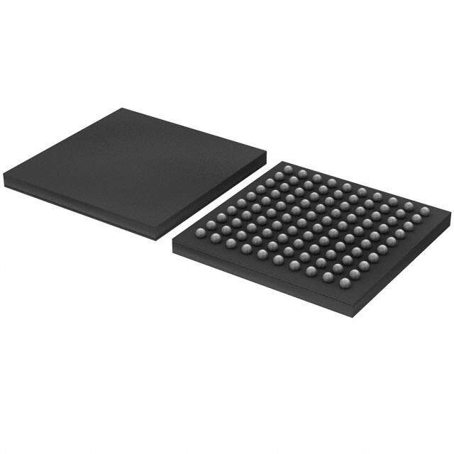
| 描述 | IC MCU 32BIT 256KB FLASH 64WLCSP |
| EEPROM容量 | - |
| 产品分类 | |
| I/O数 | 43 |
| 品牌 | Atmel |
| 数据手册 | |
| 产品图片 | |
| 产品型号 | ATSAM4LC4BA-UUR |
| RAM容量 | 32K x 8 |
| rohs | 无铅 / 符合限制有害物质指令(RoHS)规范要求 |
| 产品系列 | SAM4L |
| 产品培训模块 | http://www.digikey.cn/PTM/IndividualPTM.page?site=cn&lang=zhs&ptm=26162http://www.digikey.cn/PTM/IndividualPTM.page?site=cn&lang=zhs&ptm=26159http://www.digikey.cn/PTM/IndividualPTM.page?site=cn&lang=zhs&ptm=26180http://www.digikey.cn/PTM/IndividualPTM.page?site=cn&lang=zhs&ptm=26247 |
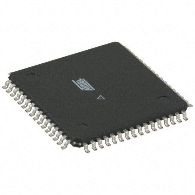
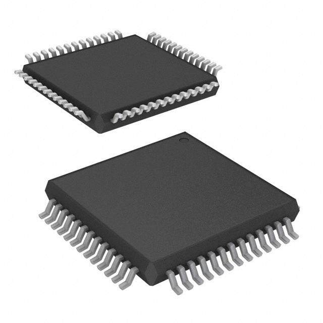
| 供应商器件封装 | 64-WLCSP |
| 其它名称 | ATSAM4LC4BA-UURCT |
| 包装 | 剪切带 (CT) |
| 外设 | 欠压检测/复位,DMA,I²S,LCD,POR,PWM,WDT |
| 封装/外壳 | 64-XFBGA,WLCSP |
| 工作温度 | -40°C ~ 85°C |
| 应用说明 | |
| 振荡器类型 | 内部 |
| 数据转换器 | A/D 7x12b, D/A 1x10b |
| 标准包装 | 1 |
| 核心处理器 | ARM® Cortex®-M4 |
| 核心尺寸 | 32-位 |
| 特色产品 | http://www.digikey.cn/product-highlights/cn/zh/atmel-sam4l-series-microcontrollers/3278 |
| 电压-电源(Vcc/Vdd) | 1.68 V ~ 3.6 V |
| 程序存储器类型 | 闪存 |
| 程序存储容量 | 256KB(256K x 8) |
| 连接性 | I²C, IrDA, LIN, SPI, UART/USART, USB |
| 速度 | 48MHz |


- 商务部:美国ITC正式对集成电路等产品启动337调查
- 曝三星4nm工艺存在良率问题 高通将骁龙8 Gen1或转产台积电
- 太阳诱电将投资9.5亿元在常州建新厂生产MLCC 预计2023年完工
- 英特尔发布欧洲新工厂建设计划 深化IDM 2.0 战略
- 台积电先进制程称霸业界 有大客户加持明年业绩稳了
- 达到5530亿美元!SIA预计今年全球半导体销售额将创下新高
- 英特尔拟将自动驾驶子公司Mobileye上市 估值或超500亿美元
- 三星加码芯片和SET,合并消费电子和移动部门,撤换高东真等 CEO
- 三星电子宣布重大人事变动 还合并消费电子和移动部门
- 海关总署:前11个月进口集成电路产品价值2.52万亿元 增长14.8%


PDF Datasheet 数据手册内容提取
Summary Atmel's SAM4L series is a member of a family of Flash microcontrollers based on the high performance 32-bit ARM Cortex-M4 RISC processor running at fre- quencies up to 48MHz. The SAM4L series embeds state-of-the-art picoPower technology for ultra-low power consumption. Combined power control techniques are used to bring active current consumption down to 90μA/MHz. The device allows a wide range of options between functionality and power consumption, giving the user the ATSAM---e ability to reach the lowest possible power consumption with the feature set required for the application. The WAIT and RETENTION modes provide full logic ARM-based and RAM retention, associated with fast wake-up capability (<1.5μs) and a very low consumption of, respectively, 3 μA and 1.5 μA. In addition, WAIT mode sup- Flash MCU ports SleepWalking features. In BACKUP mode, CPU, peripherals and RAM are powered off and, while consuming less than 0.9μA with external interrupt wake- up supported. SAM4L Series The SAM4L series offers a wide range of peripherals such as segment LCD con- troller, embedded hardware capacitive touch (QTouch), USB device & embedded host, 128-bit AES and audio interfaces in addition to high speed serial peripherals such as USART, SPI and I2C. Additionally the Peripheral Event System and SleepWalking allows the peripherals to communicate directly with each other and make intelligent decisions and decide to wake-up the system on a qualified events on a peripheral level; such as I2C address match or and ADC threshold. Features • Core Summary – ARM® CortexTM-M4 running at up to 48MHz – Memory Protection Unit (MPU) – Thumb®-2 instruction set • picoPower® Technology for Ultra-low Power Consumption – Active mode downto 90µA/MHz with configurable voltage scaling – High performance and efficiency: 28 coremark/mA – Wait mode downto 3µA with fast wake-up time (<1.5µs) supporting SleepWalking – Full RAM and Logic Retention mode downto 1.5µA with fast wake-up time (<1.5µs) – Ultra low power Backup mode with/without RTC downto 1,5/0.9µA • Memories – From 128 to 512Kbytes embedded Flash, 64-bit wide access, • 0 wait-state capability up to 24MHz – up to 64Kbytes embedded SRAM • System Functions – Embedded voltage linear and switching regulator for single supply operation – Two Power-on-Reset and Two Brown-out Detectors (BOD) – Quartz or ceramic resonator oscillators: 0.6 to 30MHz main power with Failure Detection and low power 32.768 kHz for RTC or device clock – High precision 4/8/12MHz factory trimmed internal RC oscillator – Slow Clock Internal RC oscillator as permanent low-power mode device clock – High speed 80MHz internal RC oscillator – Low power 32kHz internal RC oscillator 42023HS–11/2016
ATSAM4L8/L4/L2 – PLL up to 240MHz for device clock and for USB – Digital Frequency Locked Loop (DFLL) with wide input range – Up to 16 peripheral DMA (PDCA) channels • Peripherals – USB 2.0 Device and Embedded Host: 12 Mbps, up to 8 bidirectional Endpoints and Multi-packet Ping-pong Mode. On- Chip Transceiver – Liquid Crystal Display (LCD) Module with Capacity up to 40 Segments and up to 4 Common Terminals – One USART with ISO7816, IrDA®, RS-485, SPI, Manchester and LIN Mode – Three USART with SPI Mode – One PicoUART for extended UART wake-up capabilities in all sleep modes – Windowed Watchdog Timer (WDT) – Asynchronous Timer (AST) with Real-time Clock Capability, Counter or Calendar Mode Supported – Frequency Meter (FREQM) for Accurate Measuring of Clock Frequency – Six 16-bit Timer/Counter (TC) Channels with capture, waveform, compare and PWM mode – One Master/Slave Serial Peripheral Interface (SPI) with Chip Select Signals – Four Master and Two Slave Two-wire Interfaces (TWI), up to 3.4Mbit/s I2C-compatible – One Advanced Encryption System (AES) with 128-bit key length – One 16-channel ADC 300Ksps (ADC) with up to 12 Bits Resolution – One DAC 500Ksps (DACC) with up to 10 Bits Resolution – Four Analog Comparators (ACIFC) with Optional Window Detection – Capacitive Touch Module (CATB) supporting up to 32 buttons – Audio Bitstream DAC (ABDACB) Suitable for Stereo Audio – Inter-IC Sound (IISC) Controller, Compliant with Inter-IC Sound (I2S) Specification – Peripheral Event System for Direct Peripheral to Peripheral Communication – 32-bit Cyclic Redundancy Check Calculation Unit (CRCCU) – Random generator (TRNG) – Parallel Capture Module (PARC) – Glue Logic Controller (GLOC) • I/O – Up to 75 I/O lines with external interrupt capability (edge or level sensitivity), debouncing, glitch filtering and slew-rate control – Up to Six High-drive I/O Pins • Single 1.68-3.6V Power Supply • Packages – 100-lead LQFP, 14 x 14 mm, pitch 0.5 mm/100-ball VFBGA, 7x7 mm, pitch 0.65 mm – 64-lead LQFP, 10 x 10 mm, pitch 0.5 mm/64-pad QFN 9x9 mm, pitch 0.5 mm – 64-ball WLCSP, 4,314x4,434 mm, pitch 0.5 mm for SAM4LC4/2 and SAM4LS4/2 series – 64-ball WLCSP, 5,270x5,194 mm, pitch 0.5 mm for SAM4LC8 and SAM4LS8 series – 48-lead LQFP, 7 x 7 mm, pitch 0.5 mm/48-pad QFN 7x7 mm, pitch 0.5 mm 2 42023HS–SAM–11/2016
ATSAM4L8/L4/L2 1. Description Atmel's SAM4L series is a member of a family of Flash microcontrollers based on the high per- formance 32-bit ARM Cortex-M4 RISC processor running at frequencies up to 48MHz. The processor implements a Memory Protection Unit (MPU) and a fast and flexible interrupt con- troller for supporting modern and real-time operating systems. The ATSAM4L8/L4/L2 embeds state-of-the-art picoPower technology for ultra-low power con- sumption. Combined power control techniques are used to bring active current consumption down to 90µA/MHz. The device allows a wide range of options between functionality and power consumption, giving the user the ability to reach the lowest possible power consumption with the feature set required for the application. On-chip regulator improves power efficiency when used in swichting mode with an external inductor or can be used in linear mode if application is noise sensitive. The ATSAM4L8/L4/L2 supports 4 power saving strategies. The SLEEP mode put the CPU in idle mode and offers different sub-modes which automatically switch off/on bus clocks, PLL, oscillators. The WAIT and RETENTION modes provide full logic and RAM retention, associated with fast wake-up capability (<1.5µs) and a very low consumption of, respectively, 3 µA and 1.5 µA. In addition, WAIT mode supports SleepWalking features. In BACKUP mode, CPU, peripher- als and RAM are powered off and, while consuming less than 0.5µA, the device is able to wake- up from external interrupts. The ATSAM4L8/L4/L2 incorporates on-chip Flash tightly coupled to a low power cache (LPCACHE) for active consumption optimization and SRAM memories for fast access. The LCD controller is intended for monochrome passive liquid crystal display (LCD) with up to 4 Common terminals and up to 40 Segments terminals. Dedicated Low Power Waveform, Con- trast Control, Extended Interrupt Mode, Selectable Frame Frequency and Blink functionality are supported to offload the CPU, reduce interrupts and reduce power consumption. The controller includes integrated LCD buffers and integrated power supply voltage. The low-power and high performance capacitive touch module (CATB) is introduced to meet the demand for a low power capacitive touch solution that could be used to handle buttons, sliders and wheels. The CATB provides excellent signal performance, as well as autonomous touch and proximity detection for up to 32 sensors. This solution includes an advanced sequencer in addition to an hardware filtering unit. The Advanced Encryption Standard module (AESA) is compliant with the FIPS (Federal Infor- mation Processing Standard) Publication 197, Advanced Encryption Standard (AES), which specifies a symmetric block cipher that is used to encrypt and decrypt electronic data. Encryp- tion is the transformation of a usable message, called the plaintext, into an unreadable form, called the ciphertext. On the other hand, decryption is the transformation that recovers the plain- text from the ciphertext. AESA supports 128 bits cryptographic key sizes. The Peripheral Direct Memory Access (DMA) controller enables data transfers between periph- erals and memories without processor involvement. The Peripheral DMA controller drastically reduces processing overhead when transferring continuous and large data streams. The Peripheral Event System (PES) allows peripherals to receive, react to, and send peripheral events without CPU intervention. Asynchronous interrupts allow advanced peripheral operation in low power modes. The Power Manager (PM) improves design flexibility and security. The Power Manager supports SleepWalking functionality, by which a module can be selectively activated based on peripheral 3 42023HS–SAM–11/2016
ATSAM4L8/L4/L2 events, even in sleep modes where the module clock is stopped. Power monitoring is supported by on-chip Power-on Reset (POR18, POR33), Brown-out Detectors (BOD18, BOD33). The device features several oscillators, such as Phase Locked Loop (PLL), Digital Frequency Locked Loop (DFLL), Oscillator 0 (OSC0), Internal RC 4,8,12MHz oscillator (RCFAST), system RC oscillator (RCSYS), Internal RC 80MHz, Internal 32kHz RC and 32kHz Crystal Oscillator. Either of these oscillators can be used as source for the system clock. The DFLL is a program- mable internal oscillator from 40 to 150MHz. It can be tuned to a high accuracy if an accurate reference clock is running, e.g. the 32kHz crystal oscillator. The Watchdog Timer (WDT) will reset the device unless it is periodically serviced by the soft- ware. This allows the device to recover from a condition that has caused the system to be unstable. The Asynchronous Timer (AST) combined with the 32kHz crystal oscillator supports powerful real-time clock capabilities, with a maximum timeout of up to 136 years. The AST can operate in counter or calendar mode. The Frequency Meter (FREQM) allows accurate measuring of a clock frequency by comparing it to a known reference clock. The Full-speed USB 2.0 device and embedded host interface (USBC) supports several USB classes at the same time utilizing the rich end-point configuration. The device includes six identical 16-bit Timer/Counter (TC) channels. Each channel can be inde- pendently programmed to perform frequency measurement, event counting, interval measurement, pulse generation, delay timing, and pulse width modulation. The ATSAM4L8/L4/L2 also features many communication interfaces, like USART, SPI, or TWI, for communication intensive applications. The USART supports different communication modes, like SPI Mode and LIN Mode. A general purpose 16-channel ADC is provided, as well as four analog comparators (ACIFC). The ADC can operate in 12-bit mode at full speed. The analog comparators can be paired to detect when the sensing voltage is within or outside the defined reference window. Atmel offers the QTouch Library for embedding capacitive touch buttons, sliders, and wheels functionality. The patented charge-transfer signal acquisition offers robust sensing and includes fully debounced reporting of touch keys as well as Adjacent Key Suppression® (AKS®) technol- ogy for unambiguous detection of key events. The easy-to-use QTouch Suite toolchain allows you to explore, develop, and debug your own touch applications. The Audio Bitstream DAC (ABDACB) converts a 16-bit sample value to a digital bitstream with an average value proportional to the sample value. Two channels are supported, making the ABDAC particularly suitable for stereo audio. The Inter-IC Sound Controller (IISC) provides a 5-bit wide, bidirectional, synchronous, digital audio link with external audio devices. The controller is compliant with the Inter-IC Sound (I2S) bus specification. 4 42023HS–SAM–11/2016
ATSAM4L8/L4/L2 2. Overview 2.1 Block Diagram Figure 2-1. Block Diagram System TAP TTDCOK JTAG & IEnm-Cuilractuoirt ARM CFomrtaexx -4M84 M PHrozcessor NVIC TDI Serial Wire TMS System Management MEMORY PROTECTION UNIT Access Port Instruction/ System Data M M M S HRAM 64/32 KB CONTROLLER RAM 1A28E-Sbit DMA S HBUIGSH M SAPTEREIDX S FLASH 512/256/128 KB CONTROLLER FLASH DP USBC S LOW POWER CACHE DM 8EndPoints S S S S M CONFIGURATION REGISTERS BUS VVDVDDDDCDOOIRPOSE I/Os UNRTE XXOIRNUST3EW23G2ILTUDCLOORAH/CTSINOC3G2R3K2POWBEBBARHARCI CSINMCDKBSBKTOAGUAY-UEPNNEPCSPRBAT TKBFGREUAOEMPCRL E BHRSIDBG-PEB D BHRSIDBG-PEB C BHRSIDBG-PEB A DMADMADMA CPTTTOEWWWNRIIIUUUUT IDMMMPSSSSRMSHAAAAAAAOPAESSSRRRRLI RTTTTTTTLEEEAE0123RRRLR 012 MNRIPSTTTCOSRTCSWWSCX,X,L CM[CDKKDD3KTO..S0S]I PPAB LPU REGISTERS TWI MASTER 3 PC GENERA EXTRINNXMTDI[8..1] EXTAESCRWYOPNNANICACTTTTLIIOHCMMR URIHONEEAODRRTLRNOLETEORGRURSU PT ONTROLLER DMADMADMA INCCTTTOOEWWNNRII TT-LSSIRRCCLLOO DAASLLVVOLLEEUEE 01NRRD SCEOTIIIGTIISSMWMSWW[CDC3D[BCCS3DKO9KIIK.AA...00SP]]LH,,BCIAAPSLH NERAL PURPOSE I/Os PPPCAB BACKUP DOMAIN ENT C DMA AUDIO BDIATCSTREAM AABBDDACACLCNK[1[1...0.0]] GE POWER MANAGER V RESETN CONCTLROOCLKLER PHERAL E DMA 1IN61-2TC-EbHRiAt FANADNCCEE L ATADRDVI[G1R4GE.E.F0RP] RESET SLEEP RI CONTROLLER CONTROLLER PE DMA IN10T-EbRit FDAACCE DACOUT GCLK_IN[1:0] GCL KR[3C:0S]YS DMA CAPACMIOTIDVUEL TEOUCH SENSDEIS[69..0] RCFAST RC80M SYSITNETMER CFOANCTEROL DMA PARCAOLNLETRL OCLALPETRURE PPCCEDNPAC1T,CPAKC[7E..N0]2 XXOIUN0T0 OSC0 GENERIC GLUE LOGIC IN[7..0] DFLL CLOCK CONTROLLER OUT[1..0] PLL CLK[2..0] TIMER/COUNTER 0 B[2..0] FREQUENCY METER TIMER/COUNTER 1 A[2..0] ACAP[3..0] AC INTERFACE ACAN[3..0] ACREFN PAD_EVT[3..0] TRUE RANDOM 32-BIT CRC GENERATOR CALCULATION UNIT 5 42023HS–SAM–11/2016
ATSAM4L8/L4/L2 2.2 Configuration Summary Table 2-1. Sub Series Summary Feature ATSAM4LC ATSAM4LS SEGMENT LCD Yes No AESA Yes No USB Device + Host Device Only Table 2-2. ATSAM4LC Configuration Summary Feature ATSAM4LC8/4/2C ATSAM4LC8/4/2B ATSAM4LC8/4/2A Number of Pins 100 64 48 Max Frequency 48MHz Flash 512/256/128KB SRAM 64/32/32KB SEGMENT LCD 4x40 4x23 4x13 GPIO 75 43 27 High-drive pins 6 3 1 External Interrupts 8 + 1 NMI 1 Master + 1 TWI 2 Masters + 2 Masters/Slaves Master/Slave 3 in LC sub series USART 4 4 in LS sub series PICOUART 1 0 Peripheral DMA Channels 16 AESA 1 Peripheral Event System 1 SPI 1 Asynchronous Timers 1 Timer/Counter Channels 6 3 Parallel Capture Inputs 8 Frequency Meter 1 Watchdog Timer 1 Power Manager 1 Glue Logic LUT 2 1 6 42023HS–SAM–11/2016
ATSAM4L8/L4/L2 Table 2-2. ATSAM4LC Configuration Summary Feature ATSAM4LC8/4/2C ATSAM4LC8/4/2B ATSAM4LC8/4/2A Digital Frequency Locked Loop 20-150MHz (DFLL) Phase Locked Loop 48-240MHz (PLL) Crystal Oscillator 0.6-30MHz (OSC0) Crystal Oscillator 32kHz (OSC32K) Oscillators RC Oscillator 80MHz (RC80M) RC Oscillator 4,8,12MHz (RCFAST) RC Oscillator 115kHz (RCSYS) RC Oscillator 32kHz (RC32K) ADC 15-channel 7-channel 3-channel DAC 1-channel Analog Comparators 4 2 1 CATB Sensors 32 32 26 USB 1 Audio Bitstream DAC 1 IIS Controller 1 TQFP/QFN/ Packages TQFP/VFBGA TQFP/QFN WLCSP . Table 2-3. ATSAM4LS Configuration Summary Feature ATSAM4LS8/4/2C ATSAM4LS8/4/2B ATSAM4LS8/4/2A Number of Pins 100 64 48 Max Frequency 48MHz Flash 512/256/128KB SRAM 64/32/32KB SEGMENT LCD NA GPIO 80 48 32 High-drive pins 6 3 1 External Interrupts 8 + 1 NMI 1 Master + 1 TWI 2 Masters + 2 Masters/Slaves Master/Slave 3 in LC sub series USART 4 4 in LS sub series PICOUART 1 0 Peripheral DMA Channels 16 AESA NA Peripheral Event System 1 SPI 1 Asynchronous Timers 1 7 42023HS–SAM–11/2016
ATSAM4L8/L4/L2 Table 2-3. ATSAM4LS Configuration Summary Feature ATSAM4LS8/4/2C ATSAM4LS8/4/2B ATSAM4LS8/4/2A Timer/Counter Channels 6 3 Parallel Capture Inputs 8 Frequency Meter 1 Watchdog Timer 1 Power Manager 1 Glue Logic LUT 2 1 Digital Frequency Locked Loop 20-150MHz (DFLL) Phase Locked Loop 48-240MHz (PLL) Crystal Oscillator 0.6-30MHz (OSC0) Crystal Oscillator 32kHz (OSC32K) Oscillators RC Oscillator 80MHz (RC80M) RC Oscillator 4,8,12MHz (RCFAST) RC Oscillator 115kHz (RCSYS) RC Oscillator 32kHz (RC32K) ADC 15-channel 7-channel 3-channel DAC 1-channel Analog Comparators 4 2 1 CATB Sensors 32 32 26 USB 1 Audio Bitstream DAC 1 IIS Controller 1 TQFP/QFN/ Packages TQFP/VFBGA TQFP/QFN WLCSP 8 42023HS–SAM–11/2016
ATSAM4L8/L4/L2 3. Package and Pinout 3.1 Package The device pins are multiplexed with peripheral functions as described in Section 3.2 ”Peripheral Multiplexing on I/O lines” on page 19. 3.1.1 ATSAM4LCx Pinout Figure 3-1. ATSAM4LC TQFP100 Pinout N PB11PB10PB09PB08PC23PC22PC21PC20PA17PA16PA15PA14PA13PC19PC18PC17PC16PC15VLCDIGNDBIASLBIASHVLCDCAPLCAPH 5432109876543210987654321 7777776666666666555555555 PA18 76 50 PA12 PA19 77 49 PA11 PA20 78 48 PA10 PC24 79 47 PA09 PC25 80 46 PB07 PC26 81 45 PB06 PC27 82 44 PA08 PC28 83 43 PC14 PC29 84 42 PC13 PC30 85 41 PC12 PC31 86 40 PC11 VDDIO 87 39 PC10 VDDIO 88 38 PC09 PB12 89 37 PC08 PB13 90 36 PC07 PA21 91 35 VDDANA PA22 92 34 ADVREFP PB14 93 33 GNDANA PB15 94 32 ADVREFN PA23 95 31 PA07 PA24 96 30 PA06 VDDIO 97 29 PB05 PA25 98 28 PB04 PA26 99 27 XOUT32 GND 100 26 XIN32 1111111111222222 1234567890123456789012345 PPPPPPGVPPPPRVGVVTPPPPPPP CCCCAANDCCCAEDNDDCABBBBAA 000000DD0000SDDDDK0000000 012301 IO4562ETCO OUIN 3012345 _NR T E 9 42023HS–SAM–11/2016
ATSAM4L8/L4/L2 Figure 3-2. ATSAM4LC VFBGA100 Pinout 1 2 3 4 5 6 7 8 9 10 A VDD PA05 PA04 GND VDDIN VDDOUT PA02 VDDIO GND PC00 CORE B PB05 XIN32 PA03 TCK RESET_N PC06 PC03 PA01 PA00 GND C PB04 XOUT32 PA06 PB03 PC04 PC05 PC02 PC01 PA26 VDDIO D AD GNDANA PA07 PC10 PB01 PA23 PB14 PB15 PA25 PA24 VREFN E AD VDDANA PC08 PC11 PB02 VDDIO PB12 PB13 PA21 PA22 VREFP F PC09 PC07 PC12 PC13 PA09 PC27 PC29 PC30 PC31 VDDIO G PC14 PA08 PB06 PC19 PA15 PB08 PB09 PB10 PC26 PC28 H PB07 PA10 PA11 PC17 PA13 PA17 PC20 PC23 PC25 PA20 J CAPL PA12 PB00 BIASL PC15 PC16 PA16 PC22 PC24 PA19 K CAPH VLCD BIASH GND VLCDIN PC18 PA14 PC21 PB11 PA18 10 42023HS–SAM–11/2016
ATSAM4L8/L4/L2 Figure 3-3. ATSAM4LC WLCSP64 Pinout 1 2 3 4 5 6 7 8 A AD PB04 GNDANA VDDANA PA09 CAPL CAPH PA12 VREFP B PB03 XIN32 XOUT32 PA08 PB06 PA10 PA11 VLCD C VDDIN PB01 PA05 PA06 PA07 PB07 PA13 BIASH D VDDOUT PB00 PA04 PB05 PB12 PB08 PA14 BIASL E GND PA03 PB02 RESET_N PB13 PB09 PA15 GND F VDD TCK PA02 PB14 PA22 PB10 PA16 VLCDIN CORE G GND PA26 PA24 PA00 PA01 PA19 PA18 PA17 H VDDIO PA25 PA23 PB15 PA21 VDDIO PA20 PB11 11 42023HS–SAM–11/2016
ATSAM4L8/L4/L2 Figure 3-4. ATSAM4LC TQFP64/QFN64 Pinout N PB11PB10PB09PB08PA17PA16PA15PA14PA13VLCDIGNDBIASLBIASHVLCDCAPLCAPH 8765432109876543 4444444443333333 PA18 49 32 PA12 PA19 50 31 PA11 PA20 51 30 PA10 VDDIO 52 29 PA09 PB12 53 28 PB07 PB13 54 27 PB06 PA21 55 26 PA08 PA22 56 25 VDDANA PB14 57 24 ADVREFP PB15 58 23 GNDANA PA23 59 22 PA07 PA24 60 21 PA06 VDDIO 61 20 PB05 PA25 62 19 PB04 PA26 63 18 XOUT32 GND 64 17 XIN32 1111111 1234567890123456 PPPRVGVVTPPPPPPP AAAEDNDDCABBBBAA 000SDDDDK0000000 012EC OIN 3012345 TO U _NR T E 12 42023HS–SAM–11/2016
ATSAM4L8/L4/L2 Figure 3-5. ATSAM4LC TQFP48/QFN48 Pinout N 1716151413CDIDSLSHCDPLPH AAAAALNAALAA PPPPPVGBIBIVCC 654321098765 333333322222 PA18 37 24 PA12 PA19 38 23 PA11 PA20 39 22 PA10 VDDIO 40 21 PA09 PA21 41 20 PA08 PA22 42 19 VDDANA PA23 43 18 ADVREFP PA24 44 17 GNDANA VDDIO 45 16 PA07 PA25 46 15 PA06 PA26 47 14 XOUT32 GND 48 13 XIN32 111 123456789012 PPPRVGVVTPPP AAAEDNDDCAAA 000SDDDDK000 012EC OI 345 N TO U _R T N E 13 42023HS–SAM–11/2016
ATSAM4L8/L4/L2 3.1.2 ATSAM4LSx Pinout Figure 3-6. ATSAM4LS TQFP100 Pinout O 1110090823222120171615141319181716153130DID292827 BBBBCCCCAAAAACCCCCAADNAAA PPPPPPPPPPPPPPPPPPPPVGPPP 5432109876543210987654321 7777776666666666555555555 PA18 76 50 PA12 PA19 77 49 PA11 PA20 78 48 PA10 PC24 79 47 PA09 PC25 80 46 PB07 PC26 81 45 PB06 PC27 82 44 PA08 PC28 83 43 PC14 PC29 84 42 PC13 PC30 85 41 PC12 PC31 86 40 PC11 VDDIO 87 39 PC10 VDDIO 88 38 PC09 PB12 89 37 PC08 PB13 90 36 PC07 PA21 91 35 VDDANA PA22 92 34 ADVREFP PB14 93 33 GNDANA PB15 94 32 ADVREFN PA23 95 31 PA07 PA24 96 30 PA06 VDDIO 97 29 PB05 PA25 98 28 PB04 PA26 99 27 XOUT32 GND 100 26 XIN32 1111111111222222 1234567890123456789012345 PPPPPPGVPPPPRVGVVTPPPPPPP CCCCAANDCCCAEDNDDCABBBBAA 000000DD0000SDDDDK0000000 012301 IO4562ETCO OUIN 3012345 _NR T E 14 42023HS–SAM–11/2016
ATSAM4L8/L4/L2 Figure 3-7. ATSAM4LS VFBGA100 Pinout 1 2 3 4 5 6 7 8 9 10 A VDD PA05 PA04 GND VDDIN VDDOUT PA02 VDDIO GND PC00 CORE B PB05 XIN32 PA03 TCK RESET_N PC06 PC03 PA01 PA00 GND C PB04 XOUT32 PA06 PB03 PC04 PC05 PC02 PC01 PA26 VDDIO D AD GNDANA PA07 PC10 PB01 PA23 PB14 PB15 PA25 PA24 VREFN E AD VDDANA PC08 PC11 PB02 VDDIO PB12 PB13 PA21 PA22 VREFP F PC09 PC07 PC12 PC13 PA09 PC27 PC29 PC30 PC31 VDDIO G PC14 PA08 PB06 PC19 PA15 PB08 PB09 PB10 PC26 PC28 H PB07 PA10 PA11 PC17 PA13 PA17 PC20 PC23 PC25 PA20 J PA28 PA12 PB00 VDDIO PC15 PC16 PA16 PC22 PC24 PA19 K PA27 PA29 GND PA30 PA31 PC18 PA14 PC21 PB11 PA18 15 42023HS–SAM–11/2016
ATSAM4L8/L4/L2 Figure 3-8. ATSAM4LS WLCSP64 Pinout 1 2 3 4 5 6 7 8 A AD PB04 GNDANA VDDANA PA09 PA28 PA27 PA12 VREFP B PB03 XIN32 XOUT32 PA08 PB06 PA10 PA11 PA29 C VDDIN PB01 PA05 PA06 PA07 PB07 PA13 GND D VDDOUT PB00 PA04 PB05 PB12 PB08 PA14 VDDIO E GND PA03 PB02 RESET_N PB13 PB09 PA15 PA30 F VDD TCK PA02 PB14 PA22 PB10 PA16 PA31 CORE G GND PA26 PA24 PA00 PA01 PA19 PA18 PA17 H VDDIO PA25 PA23 PB15 PA21 VDDIO PA20 PB11 16 42023HS–SAM–11/2016
ATSAM4L8/L4/L2 Figure 3-9. ATSAM4LS TQFP64/QFN64 Pinout O 1110090817161514133130DID292827 BBBBAAAAAAADNAAA PPPPPPPPPPPVGPPP 8765432109876543 4444444443333333 PA18 49 32 PA12 PA19 50 31 PA11 PA20 51 30 PA10 VDDIO 52 29 PA09 PB12 53 28 PB07 PB13 54 27 PB06 PA21 55 26 PA08 PA22 56 25 VDDANA PB14 57 24 ADVREFP PB15 58 23 GNDANA PA23 59 22 PA07 PA24 60 21 PA06 VDDIO 61 20 PB05 PA25 62 19 PB04 PA26 63 18 XOUT32 GND 64 17 XIN32 1111111 1234567890123456 PPPRVGVVTPPPPPPP AAAEDNDDCABBBBAA 000SDDDDK0000000 012ETCO OUIN 3012345 _NR T E 17 42023HS–SAM–11/2016
ATSAM4L8/L4/L2 Figure 3-10. ATSAM4LS TQFP48/QFN48 Pinout O 17161514133130DID292827 AAAAAAADNAAA PPPPPPPVGPPP 654321098765 333333322222 PA18 37 24 PA12 PA19 38 23 PA11 PA20 39 22 PA10 VDDIO 40 21 PA09 PA21 41 20 PA08 PA22 42 19 VDDANA PA23 43 18 ADVREFP PA24 44 17 GNDANA VDDIO 45 16 PA07 PA25 46 15 PA06 PA26 47 14 XOUT32 GND 48 13 XIN32 111 123456789012 PPPRVGVVTPPP AAAEDNDDCAAA 000SDDDDK000 012EC OIN 345 TO U _NR T E See Section 3.3 ”Signals Description” on page 31 for a description of the various peripheral signals. Refer to ”Electrical Characteristics” on page 99 for a description of the electrical properties of the pin types used. 18 42023HS–SAM–11/2016
ATSAM4L8/L4/L2 3.2 Peripheral Multiplexing on I/O lines 3.2.1 Multiplexed Signals Each GPIO line can be assigned to one of the peripheral functions. The following tables (Section 3-1 ”100-pin GPIO Controller Function Multiplexing” on page 19 to Section 3-4 ”48-pin GPIO Controller Function Multiplexing” on page 28) describes the peripheral signals multiplexed to the GPIO lines. Peripheral functions that are not relevant in some parts of the family are grey-shaded. For description of differents Supply voltage source, refer to the Section 6. ”Power and Startup Considerations” on page 46. Table 3-1. 100-pin GPIO Controller Function Multiplexing (Sheet 1 of 4) C S L L 4 4 M M y ATSA ATSA Pin GPIO Suppl GPIO Functions QFN VFBGA QFN VFBGA A B C D E F G 5 B9 5 B9 PA00 0 VDDIO 6 B8 6 B8 PA01 1 VDDIO SCIF SPI CATB 12 A7 12 A7 PA02 2 VDDIN GCLK0 NPCS0 DIS SPI 19 B3 19 B3 PA03 3 VDDIN MISO ADCIFE USART0 EIC GLOC CATB 24 A2 24 A2 PA04 4 VDDANA AD0 CLK EXTINT2 IN1 SENSE0 ADCIFE USART0 EIC GLOC ADCIFE CATB 25 A1 25 A1 PA05 5 VDDANA AD1 RXD EXTINT3 IN2 TRIGGER SENSE1 DACC USART0 EIC GLOC ACIFC CATB 30 C3 30 C3 PA06 6 VDDANA VOUT RTS EXTINT1 IN0 ACAN0 SENSE2 ADCIFE USART0 EIC GLOC ACIFC CATB 31 D3 31 D3 PA07 7 VDDANA AD2 TXD EXTINT4 IN3 ACAP0 SENSE3 USART0 TC0 PEVC GLOC LCDCA CATB 44 G2 44 G2 PA08 8 LCDA RTS A0 PAD EVT0 OUT0 SEG23 SENSE4 USART0 TC0 PEVC PARC LCDCA CATB 47 F5 47 F5 PA09 9 LCDA CTS B0 PAD EVT1 PCDATA0 COM3 SENSE5 USART0 TC0 PEVC PARC LCDCA CATB 48 H2 48 H2 PA10 10 LCDA CLK A1 PAD EVT2 PCDATA1 COM2 SENSE6 USART0 TC0 PEVC PARC LCDCA CATB 49 H3 49 H3 PA11 11 LCDA RXD B1 PAD EVT3 PCDATA2 COM1 SENSE7 USART0 TC0 PARC LCDCA CATB 50 J2 50 J2 PA12 12 LCDA TXD A2 PCDATA3 COM0 DIS USART1 TC0 SPI PARC LCDCA CATB 63 H5 63 H5 PA13 13 LCDA RTS B2 NPCS1 PCDATA4 SEG5 SENSE8 USART1 TC0 SPI PARC LCDCA CATB 64 K7 64 K7 PA14 14 LCDA CLK CLK0 NPCS2 PCDATA5 SEG6 SENSE9 USART1 TC0 SPI PARC LCDCA CATB 65 G5 65 G5 PA15 15 LCDA RXD CLK1 NPCS3 PCDATA6 SEG7 SENSE10 19 42023HS–SAM–11/2016
ATSAM4L8/L4/L2 Table 3-1. 100-pin GPIO Controller Function Multiplexing (Sheet 2 of 4) C S L L 4 4 M M y ATSA ATSA Pin GPIO Suppl GPIO Functions QFN VFBGA QFN VFBGA A B C D E F G USART1 TC0 EIC PARC LCDCA CATB 66 J7 66 J7 PA16 16 LCDA TXD CLK2 EXTINT1 PCDATA7 SEG8 SENSE11 USART2 ABDACB EIC PARC LCDCA CATB 67 H6 67 H6 PA17 17 LCDA RTS DAC0 EXTINT2 PCCK SEG9 SENSE12 USART2 ABDACB EIC PARC LCDCA CATB 76 K10 76 K10 PA18 18 LCDA CLK DACN0 EXTINT3 PCEN1 SEG18 SENSE13 USART2 ABDACB EIC PARC SCIF LCDCA CATB 77 J10 77 J10 PA19 19 LCDA RXD DAC1 EXTINT4 PCEN2 GCLK0 SEG19 SENSE14 USART2 ABDACB EIC GLOC SCIF LCDCA CATB 78 H10 78 H10 PA20 20 LCDA TXD DACN1 EXTINT5 IN0 GCLK1 SEG20 SENSE15 SPI USART1 EIC GLOC TWIM2 LCDCA CATB 91 E9 91 E9 PA21 21 LCDC MISO CTS EXTINT6 IN1 TWD SEG34 SENSE16 SPI USART2 EIC GLOC TWIM2 LCDCA CATB 92 E10 92 E10 PA22 22 LCDC MOSI CTS EXTINT7 IN2 TWCK SEG35 SENSE17 SPI TWIMS0 EIC GLOC SCIF LCDCA CATB 95 D6 95 D6 PA23 23 LCDC SCK TWD EXTINT8 IN3 GCLK IN0 SEG38 DIS SPI TWIMS0 GLOC SCIF LCDCA CATB 96 D10 96 D10 PA24 24 LCDC NPCS0 TWCK OUT0 GCLK IN1 SEG39 SENSE18 USBC USART2 CATB 98 D9 98 D9 PA25 25 VDDIO DM RXD SENSE19 USBC USART2 CATB 99 C9 99 C9 PA26 26 VDDIO DP TXD SENSE20 SPI IISC ABDACB GLOC USART3 CATB 51 K1 PA27 27 LCDA MISO ISCK DAC0 IN4 RTS SENSE0 SPI IISC ABDACB GLOC USART3 CATB 52 J1 PA28 28 LCDA MOSI ISDI DACN0 IN5 CTS SENSE1 SPI IISC ABDACB GLOC USART3 CATB 53 K2 PA29 29 LCDA SCK IWS DAC1 IN6 CLK SENSE2 SPI IISC ABDACB GLOC USART3 CATB 56 K4 PA30 30 LCDA NPCS0 ISDO DACN1 IN7 RXD SENSE3 SPI IISC ABDACB GLOC USART3 CATB 57 K5 PA31 31 LCDA NPCS1 IMCK CLK OUT1 TXD DIS TWIMS1 USART0 CATB 20 J3 20 J3 PB00 32 VDDIN TWD RXD SENSE21 TWIMS1 USART0 EIC CATB 21 D5 21 D5 PB01 33 VDDIN TWCK TXD EXTINT0 SENSE22 ADCIFE USART1 ABDACB IISC ACIFC CATB 22 E5 22 E5 PB02 34 VDDANA AD3 RTS DAC0 ISCK ACBN0 SENSE23 ADCIFE USART1 ABDACB IISC ACIFC CATB 23 C4 23 C4 PB03 35 VDDANA AD4 CLK DACN0 ISDI ACBP0 DIS ADCIFE USART1 ABDACB IISC DACC CATB 28 C1 28 C1 PB04 36 VDDANA AD5 RXD DAC1 ISDO EXT TRIG0 SENSE24 ADCIFE USART1 ABDACB IISC CATB 29 B1 29 B1 PB05 37 VDDANA AD6 TXD DACN1 IMCK SENSE25 USART3 GLOC IISC LCDCA CATB 45 G3 45 G3 PB06 38 LCDA RTS IN4 IWS SEG22 SENSE26 USART3 GLOC TC0 LCDCA CATB 46 H1 46 H1 PB07 39 LCDA CTS IN5 A0 SEG21 SENSE27 20 42023HS–SAM–11/2016
ATSAM4L8/L4/L2 Table 3-1. 100-pin GPIO Controller Function Multiplexing (Sheet 3 of 4) C S L L 4 4 M M y ATSA ATSA Pin GPIO Suppl GPIO Functions QFN VFBGA QFN VFBGA A B C D E F G USART3 GLOC TC0 LCDCA CATB 72 G6 72 G6 PB08 40 LCDA CLK IN6 B0 SEG14 SENSE28 USART3 PEVC GLOC TC0 LCDCA CATB 73 G7 73 G7 PB09 41 LCDA RXD PAD EVT2 IN7 A1 SEG15 SENSE29 USART3 PEVC GLOC TC0 SCIF LCDCA CATB 74 G8 74 G8 PB10 42 LCDA TXD PAD EVT3 OUT1 B1 GCLK0 SEG16 SENSE30 USART0 SPI TC0 SCIF LCDCA CATB 75 K9 75 K9 PB11 43 LCDA CTS NPCS2 A2 GCLK1 SEG17 SENSE31 USART0 SPI PEVC TC0 SCIF LCDCA CATB 89 E7 89 E7 PB12 44 LCDC RTS NPCS3 PAD EVT0 B2 GCLK2 SEG32 DIS USART0 SPI PEVC TC0 SCIF LCDCA CATB 90 E8 90 E8 PB13 45 LCDC CLK NPCS1 PAD EVT1 CLK0 GCLK3 SEG33 SENSE0 USART0 SPI TWIM3 TC0 SCIF LCDCA CATB 93 D7 93 D7 PB14 46 LCDC RXD MISO TWD CLK1 GCLK IN0 SEG36 SENSE1 USART0 SPI TWIM3 TC0 SCIF LCDCA CATB 94 D8 94 D8 PB15 47 LCDC TXD MOSI TWCK CLK2 GCLK IN1 SEG37 SENSE2 SPI USART0 TC1 CATB 1 A10 1 A10 PC00 64 VDDIO NPCS2 CLK A0 SENSE3 SPI USART0 TC1 CATB 2 C8 2 C8 PC01 65 VDDIO NPCS3 RTS B0 SENSE4 SPI USART0 USART0 TC1 CATB 3 C7 3 C7 PC02 66 VDDIO NPCS1 CTS RXD A1 SENSE5 SPI EIC USART0 TC1 CATB 4 B7 4 B7 PC03 67 VDDIO NPCS0 EXTINT5 TXD B1 SENSE6 SPI EIC TC1 CATB 9 C5 9 C5 PC04 68 VDDIO MISO EXTINT6 A2 SENSE7 SPI EIC TC1 CATB 10 C6 10 C6 PC05 69 VDDIO MOSI EXTINT7 B2 DIS SPI EIC TC1 CATB 11 B6 11 B6 PC06 70 VDDIO SCK EXTINT8 CLK0 SENSE8 ADCIFE USART2 PEVC TC1 CATB 36 F2 36 F2 PC07 71 VDDANA AD7 RTS PAD EVT0 CLK1 SENSE9 ADCIFE USART2 PEVC TC1 USART2 CATB 37 E3 37 E3 PC08 72 VDDANA AD8 CLK PAD EVT1 CLK2 CTS SENSE10 ADCIFE USART3 ABDACB IISC ACIFC CATB 38 F1 38 F1 PC09 73 VDDANA AD9 RXD DAC0 ISCK ACAN1 SENSE11 ADCIFE USART3 ABDACB IISC ACIFC CATB 39 D4 39 D4 PC10 74 VDDANA AD10 TXD DACN0 ISDI ACAP1 SENSE12 ADCIFE USART2 PEVC CATB 40 E4 40 E4 PC11 75 VDDANA AD11 RXD PAD EVT2 SENSE13 ADCIFE USART2 ABDACB IISC CATB 41 F3 41 F3 PC12 76 VDDANA AD12 TXD CLK IWS SENSE14 ADCIFE USART3 ABDACB IISC ACIFC CATB 42 F4 42 F4 PC13 77 VDDANA AD13 RTS DAC1 ISDO ACBN1 SENSE15 ADCIFE USART3 ABDACB IISC ACIFC CATB 43 G1 43 G1 PC14 78 VDDANA AD14 CLK DACN1 IMCK ACBP1 DIS TC1 GLOC LCDCA CATB 58 J5 58 J5 PC15 79 LCDA A0 IN4 SEG0 SENSE16 21 42023HS–SAM–11/2016
ATSAM4L8/L4/L2 Table 3-1. 100-pin GPIO Controller Function Multiplexing (Sheet 4 of 4) C S L L 4 4 M M y ATSA ATSA Pin GPIO Suppl GPIO Functions QFN VFBGA QFN VFBGA A B C D E F G TC1 GLOC LCDCA CATB 59 J6 59 J6 PC16 80 LCDA B0 IN5 SEG1 SENSE17 TC1 GLOC LCDCA CATB 60 H4 60 H4 PC17 81 LCDA A1 IN6 SEG2 SENSE18 TC1 GLOC LCDCA CATB 61 K6 61 K6 PC18 82 LCDA B1 IN7 SEG3 SENSE19 TC1 GLOC LCDCA CATB 62 G4 62 G4 PC19 83 LCDA A2 OUT1 SEG4 SENSE20 TC1 LCDCA CATB 68 H7 68 H7 PC20 84 LCDA B2 SEG10 SENSE21 TC1 PARC LCDCA CATB 69 K8 69 K8 PC21 85 LCDA CLK0 PCCK SEG11 SENSE22 TC1 PARC LCDCA CATB 70 J8 70 J8 PC22 86 LCDA CLK1 PCEN1 SEG12 SENSE23 TC1 PARC LCDCA CATB 71 H8 71 H8 PC23 87 LCDA CLK2 PCEN2 SEG13 DIS USART1 EIC PEVC PARC LCDCA CATB 79 J9 79 J9 PC24 88 LCDB RTS EXTINT1 PAD EVT0 PCDATA0 SEG24 SENSE24 USART1 EIC PEVC PARC LCDCA CATB 80 H9 80 H9 PC25 89 LCDB CLK EXTINT2 PAD EVT1 PCDATA1 SEG25 SENSE25 USART1 EIC PEVC PARC SCIF LCDCA CATB 81 G9 81 G9 PC26 90 LCDB RXD EXTINT3 PAD EVT2 PCDATA2 GCLK0 SEG26 SENSE26 USART1 EIC PEVC PARC SCIF LCDCA CATB 82 F6 82 F6 PC27 91 LCDB TXD EXTINT4 PAD EVT3 PCDATA3 GCLK1 SEG27 SENSE27 USART3 SPI GLOC PARC SCIF LCDCA CATB 83 G10 83 G10 PC28 92 LCDB RXD MISO IN4 PCDATA4 GCLK2 SEG28 SENSE28 USART3 SPI GLOC PARC SCIF LCDCA CATB 84 F7 84 F7 PC29 93 LCDB TXD MOSI IN5 PCDATA5 GCLK3 SEG29 SENSE29 USART3 SPI GLOC PARC SCIF LCDCA CATB 85 F8 85 F8 PC30 94 LCDB RTS SCK IN6 PCDATA6 GCLK IN0 SEG30 SENSE30 USART3 SPI GLOC PARC SCIF LCDCA CATB 86 F9 86 F9 PC31 95 LCDB CLK NPCS0 OUT1 PCDATA7 GCLK IN1 SEG31 SENSE31 Table 3-2. 64-pin GPIO Controller Function Multiplexing (Sheet 1 of 3) C S L L 4 4 M M ATSA ATSA Pin GPIO upply GPIO Functions S QFP QFP QFN QFN A B C D E F G 1 1 PA00 0 VDDIO 2 2 PA01 1 VDDIO SCIF SPI CATB 3 3 PA02 2 VDDIN GCLK0 NPCS0 DIS SPI 10 10 PA03 3 VDDIN MISO 22 42023HS–SAM–11/2016
ATSAM4L8/L4/L2 Table 3-2. 64-pin GPIO Controller Function Multiplexing (Sheet 2 of 3) C S L L 4 4 M M ATSA ATSA Pin GPIO upply GPIO Functions S QFP QFP QFN QFN A B C D E F G ADCIFE USART0 EIC GLOC CATB 15 15 PA04 4 VDDANA AD0 CLK EXTINT2 IN1 SENSE0 ADCIFE USART0 EIC GLOC ADCIFE CATB 16 16 PA05 5 VDDANA AD1 RXD EXTINT3 IN2 TRIGGER SENSE1 DACC USART0 EIC GLOC ACIFC CATB 21 21 PA06 6 VDDANA VOUT RTS EXTINT1 IN0 ACAN0 SENSE2 ADCIFE USART0 EIC GLOC ACIFC CATB 22 22 PA07 7 VDDANA AD2 TXD EXTINT4 IN3 ACAP0 SENSE3 USART0 TC0 PEVC GLOC LCDCA CATB 26 26 PA08 8 LCDA RTS A0 PAD EVT0 OUT0 SEG23 SENSE4 USART0 TC0 PEVC PARC LCDCA CATB 29 29 PA09 9 LCDA CTS B0 PAD EVT1 PCDATA0 COM3 SENSE5 USART0 TC0 PEVC PARC LCDCA CATB 30 30 PA10 10 LCDA CLK A1 PAD EVT2 PCDATA1 COM2 SENSE6 USART0 TC0 PEVC PARC LCDCA CATB 31 31 PA11 11 LCDA RXD B1 PAD EVT3 PCDATA2 COM1 SENSE7 USART0 TC0 PARC LCDCA CATB 32 32 PA12 12 LCDA TXD A2 PCDATA3 COM0 DIS USART1 TC0 SPI PARC LCDCA CATB 40 40 PA13 13 LCDA RTS B2 NPCS1 PCDATA4 SEG5 SENSE8 USART1 TC0 SPI PARC LCDCA CATB 41 41 PA14 14 LCDA CLK CLK0 NPCS2 PCDATA5 SEG6 SENSE9 USART1 TC0 SPI PARC LCDCA CATB 42 42 PA15 15 LCDA RXD CLK1 NPCS3 PCDATA6 SEG7 SENSE10 USART1 TC0 EIC PARC LCDCA CATB 43 43 PA16 16 LCDA TXD CLK2 EXTINT1 PCDATA7 SEG8 SENSE11 USART2 ABDACB EIC PARC LCDCA CATB 44 44 PA17 17 LCDA RTS DAC0 EXTINT2 PCCK SEG9 SENSE12 USART2 ABDACB EIC PARC LCDCA CATB 49 49 PA18 18 LCDA CLK DACN0 EXTINT3 PCEN1 SEG18 SENSE13 USART2 ABDACB EIC PARC SCIF LCDCA CATB 50 50 PA19 19 LCDA RXD DAC1 EXTINT4 PCEN2 GCLK0 SEG19 SENSE14 USART2 ABDACB EIC GLOC SCIF LCDCA CATB 51 51 PA20 20 LCDA TXD DACN1 EXTINT5 IN0 GCLK1 SEG20 SENSE15 SPI USART1 EIC GLOC TWIM2 LCDCA CATB 55 55 PA21 21 LCDC MISO CTS EXTINT6 IN1 TWD SEG34 SENSE16 SPI USART2 EIC GLOC TWIM2 LCDCA CATB 56 56 PA22 22 LCDC MOSI CTS EXTINT7 IN2 TWCK SEG35 SENSE17 SPI TWIMS0 EIC GLOC SCIF LCDCA CATB 59 59 PA23 23 LCDC SCK TWD EXTINT8 IN3 GCLK IN0 SEG38 DIS SPI TWIMS0 GLOC SCIF LCDCA CATB 60 60 PA24 24 LCDC NPCS0 TWCK OUT0 GCLK IN1 SEG39 SENSE18 USBC USART2 CATB 62 62 PA25 25 VDDIO DM RXD SENSE19 USBC USART2 CATB 63 63 PA26 26 VDDIO DP TXD SENSE20 23 42023HS–SAM–11/2016
ATSAM4L8/L4/L2 Table 3-2. 64-pin GPIO Controller Function Multiplexing (Sheet 3 of 3) C S L L 4 4 M M ATSA ATSA Pin GPIO upply GPIO Functions S QFP QFP QFN QFN A B C D E F G SPI IISC ABDACB GLOC USART3 CATB 33 PA27 27 LCDA MISO ISCK DAC0 IN4 RTS SENSE0 SPI IISC ABDACB GLOC USART3 CATB 34 PA28 28 LCDA MOSI ISDI DACN0 IN5 CTS SENSE1 SPI IISC ABDACB GLOC USART3 CATB 35 PA29 29 LCDA SCK IWS DAC1 IN6 CLK SENSE2 SPI IISC ABDACB GLOC USART3 CATB 38 PA30 30 LCDA NPCS0 ISDO DACN1 IN7 RXD SENSE3 SPI IISC ABDACB GLOC USART3 CATB 39 PA31 31 LCDA NPCS1 IMCK CLK OUT1 TXD DIS TWIMS1 USART0 CATB 11 11 PB00 32 VDDIN TWD RXD SENSE21 TWIMS1 USART0 EIC CATB 12 12 PB01 33 VDDIN TWCK TXD EXTINT0 SENSE22 ADCIFE USART1 ABDACB IISC ACIFC CATB 13 13 PB02 34 VDDANA AD3 RTS DAC0 ISCK ACBN0 SENSE23 ADCIFE USART1 ABDACB IISC ACIFC CATB 14 14 PB03 35 VDDANA AD4 CLK DACN0 ISDI ACBP0 DIS ADCIFE USART1 ABDACB IISC DACC CATB 19 19 PB04 36 VDDANA AD5 RXD DAC1 ISDO EXT TRIG0 SENSE24 ADCIFE USART1 ABDACB IISC CATB 20 20 PB05 37 VDDANA AD6 TXD DACN1 IMCK SENSE25 USART3 GLOC IISC LCDCA CATB 27 27 PB06 38 LCDA RTS IN4 IWS SEG22 SENSE26 USART3 GLOC TC0 LCDCA CATB 28 28 PB07 39 LCDA CTS IN5 A0 SEG21 SENSE27 USART3 GLOC TC0 LCDCA CATB 45 45 PB08 40 LCDA CLK IN6 B0 SEG14 SENSE28 USART3 PEVC GLOC TC0 LCDCA CATB 46 46 PB09 41 LCDA RXD PAD EVT2 IN7 A1 SEG15 SENSE29 USART3 PEVC GLOC TC0 SCIF LCDCA CATB 47 47 PB10 42 LCDA TXD PAD EVT3 OUT1 B1 GCLK0 SEG16 SENSE30 USART0 SPI TC0 SCIF LCDCA CATB 48 48 PB11 43 LCDA CTS NPCS2 A2 GCLK1 SEG17 SENSE31 USART0 SPI PEVC TC0 SCIF LCDCA CATB 53 53 PB12 44 LCDC RTS NPCS3 PAD EVT0 B2 GCLK2 SEG32 DIS USART0 SPI PEVC TC0 SCIF LCDCA CATB 54 54 PB13 45 LCDC CLK NPCS1 PAD EVT1 CLK0 GCLK3 SEG33 SENSE0 USART0 SPI TWIM3 TC0 SCIF LCDCA CATB 57 57 PB14 46 LCDC RXD MISO TWD CLK1 GCLK IN0 SEG36 SENSE1 USART0 SPI TWIM3 TC0 SCIF LCDCA CATB 58 58 PB15 47 LCDC TXD MOSI TWCK CLK2 GCLK IN1 SEG37 SENSE2 24 42023HS–SAM–11/2016
ATSAM4L8/L4/L2 Table 3-3. 64-pin GPIO Controller Function Multiplexing for WLCSP package (Sheet 1 of 3) C S L L 4 4 M M y TSA TSA Pin GPIO uppl GPIO Functions A A S WLCSP WLCSP A B C D E F G G4 G4 PA00 0 VDDIO G5 G5 PA01 1 VDDIO SCIF SPI CATB F3 F3 PA02 2 VDDIN GCLK0 NPCS0 DIS SPI E2 E2 PA03 3 VDDIN MISO ADCIFE USART0 EIC GLOC CATB D3 D3 PA04 4 VDDANA AD0 CLK EXTINT2 IN1 SENSE0 ADCIFE USART0 EIC GLOC ADCIFE CATB C3 C3 PA05 5 VDDANA AD1 RXD EXTINT3 IN2 TRIGGER SENSE1 DACC USART0 EIC GLOC ACIFC CATB C4 C4 PA06 6 VDDANA VOUT RTS EXTINT1 IN0 ACAN0 SENSE2 ADCIFE USART0 EIC GLOC ACIFC CATB C5 C5 PA07 7 VDDANA AD2 TXD EXTINT4 IN3 ACAP0 SENSE3 USART0 TC0 PEVC GLOC LCDCA CATB B4 B4 PA08 8 LCDA RTS A0 PAD EVT0 OUT0 SEG23 SENSE4 USART0 TC0 PEVC PARC LCDCA CATB A5 A5 PA09 9 LCDA CTS B0 PAD EVT1 PCDATA0 COM3 SENSE5 USART0 TC0 PEVC PARC LCDCA CATB B6 B6 PA10 10 LCDA CLK A1 PAD EVT2 PCDATA1 COM2 SENSE6 USART0 TC0 PEVC PARC LCDCA CATB B7 B7 PA11 11 LCDA RXD B1 PAD EVT3 PCDATA2 COM1 SENSE7 USART0 TC0 PARC LCDCA CATB A8 A8 PA12 12 LCDA TXD A2 PCDATA3 COM0 DIS USART1 TC0 SPI PARC LCDCA CATB C7 C7 PA13 13 LCDA RTS B2 NPCS1 PCDATA4 SEG5 SENSE8 USART1 TC0 SPI PARC LCDCA CATB D7 D7 PA14 14 LCDA CLK CLK0 NPCS2 PCDATA5 SEG6 SENSE9 USART1 TC0 SPI PARC LCDCA CATB E7 E7 PA15 15 LCDA RXD CLK1 NPCS3 PCDATA6 SEG7 SENSE10 USART1 TC0 EIC PARC LCDCA CATB F7 F7 PA16 16 LCDA TXD CLK2 EXTINT1 PCDATA7 SEG8 SENSE11 USART2 ABDACB EIC PARC LCDCA CATB G8 G8 PA17 17 LCDA RTS DAC0 EXTINT2 PCCK SEG9 SENSE12 USART2 ABDACB EIC PARC LCDCA CATB G7 G7 PA18 18 LCDA CLK DACN0 EXTINT3 PCEN1 SEG18 SENSE13 USART2 ABDACB EIC PARC SCIF LCDCA CATB G6 G6 PA19 19 LCDA RXD DAC1 EXTINT4 PCEN2 GCLK0 SEG19 SENSE14 USART2 ABDACB EIC GLOC SCIF LCDCA CATB H7 H7 PA20 20 LCDA TXD DACN1 EXTINT5 IN0 GCLK1 SEG20 SENSE15 SPI USART1 EIC GLOC TWIM2 LCDCA CATB H5 H5 PA21 21 LCDC MISO CTS EXTINT6 IN1 TWD SEG34 SENSE16 SPI USART2 EIC GLOC TWIM2 LCDCA CATB F5 F5 PA22 22 LCDC MOSI CTS EXTINT7 IN2 TWCK SEG35 SENSE17 25 42023HS–SAM–11/2016
ATSAM4L8/L4/L2 Table 3-3. 64-pin GPIO Controller Function Multiplexing for WLCSP package (Sheet 2 of 3) C S L L 4 4 M M y TSA TSA Pin GPIO uppl GPIO Functions A A S WLCSP WLCSP A B C D E F G SPI TWIMS0 EIC GLOC SCIF LCDCA CATB H3 H3 PA23 23 LCDC SCK TWD EXTINT8 IN3 GCLK IN0 SEG38 DIS SPI TWIMS0 GLOC SCIF LCDCA CATB G3 G3 PA24 24 LCDC NPCS0 TWCK OUT0 GCLK IN1 SEG39 SENSE18 USBC USART2 CATB H2 H2 PA25 25 VDDIO DM RXD SENSE19 USBC USART2 CATB G2 G2 PA26 26 VDDIO DP TXD SENSE20 SPI IISC ABDACB GLOC USART3 CATB A7 PA27 27 LCDA MISO ISCK DAC0 IN4 RTS SENSE0 SPI IISC ABDACB GLOC USART3 CATB A6 PA28 28 LCDA MOSI ISDI DACN0 IN5 CTS SENSE1 SPI IISC ABDACB GLOC USART3 CATB B8 PA29 29 LCDA SCK IWS DAC1 IN6 CLK SENSE2 SPI IISC ABDACB GLOC USART3 CATB E8 PA30 30 LCDA NPCS0 ISDO DACN1 IN7 RXD SENSE3 SPI IISC ABDACB GLOC USART3 CATB F8 PA31 31 LCDA NPCS1 IMCK CLK OUT1 TXD DIS TWIMS1 USART0 CATB D2 D2 PB00 32 VDDIN TWD RXD SENSE21 TWIMS1 USART0 EIC CATB C2 C2 PB01 33 VDDIN TWCK TXD EXTINT0 SENSE22 ADCIFE USART1 ABDACB IISC ACIFC CATB E3 E3 PB02 34 VDDANA AD3 RTS DAC0 ISCK ACBN0 SENSE23 ADCIFE USART1 ABDACB IISC ACIFC CATB B1 B1 PB03 35 VDDANA AD4 CLK DACN0 ISDI ACBP0 DIS ADCIFE USART1 ABDACB IISC DACC CATB A1 A1 PB04 36 VDDANA AD5 RXD DAC1 ISDO EXT TRIG0 SENSE24 ADCIFE USART1 ABDACB IISC CATB D4 D4 PB05 37 VDDANA AD6 TXD DACN1 IMCK SENSE25 USART3 GLOC IISC LCDCA CATB B5 B5 PB06 38 LCDA RTS IN4 IWS SEG22 SENSE26 USART3 GLOC TC0 LCDCA CATB C6 C6 PB07 39 LCDA CTS IN5 A0 SEG21 SENSE27 USART3 GLOC TC0 LCDCA CATB D6 D6 PB08 40 LCDA CLK IN6 B0 SEG14 SENSE28 USART3 PEVC GLOC TC0 LCDCA CATB E6 E6 PB09 41 LCDA RXD PAD EVT2 IN7 A1 SEG15 SENSE29 USART3 PEVC GLOC TC0 SCIF LCDCA CATB F6 F6 PB10 42 LCDA TXD PAD EVT3 OUT1 B1 GCLK0 SEG16 SENSE30 USART0 SPI TC0 SCIF LCDCA CATB H8 H8 PB11 43 LCDA CTS NPCS2 A2 GCLK1 SEG17 SENSE31 USART0 SPI PEVC TC0 SCIF LCDCA CATB D5 D5 PB12 44 LCDC RTS NPCS3 PAD EVT0 B2 GCLK2 SEG32 DIS 26 42023HS–SAM–11/2016
ATSAM4L8/L4/L2 Table 3-3. 64-pin GPIO Controller Function Multiplexing for WLCSP package (Sheet 3 of 3) C S L L 4 4 M M y TSA TSA Pin GPIO uppl GPIO Functions A A S WLCSP WLCSP A B C D E F G USART0 SPI PEVC TC0 SCIF LCDCA CATB E5 E5 PB13 45 LCDC CLK NPCS1 PAD EVT1 CLK0 GCLK3 SEG33 SENSE0 USART0 SPI TWIM3 TC0 SCIF LCDCA CATB F4 F4 PB14 46 LCDC RXD MISO TWD CLK1 GCLK IN0 SEG36 SENSE1 USART0 SPI TWIM3 TC0 SCIF LCDCA CATB H4 H4 PB15 47 LCDC TXD MOSI TWCK CLK2 GCLK IN1 SEG37 SENSE2 27 42023HS–SAM–11/2016
ATSAM4L8/L4/L2 Table 3-4. 48-pin GPIO Controller Function Multiplexing (Sheet 1 of 2) TSAM4LC TSAM4LS Pin GPIO Supply A B C GPIO FuDnctions E F G A A 1 1 PA00 0 VDDIO 2 2 PA01 1 VDDIO SCIF SPI CATB 3 3 PA02 2 VDDIN GCLK0 NPCS0 DIS SPI 10 10 PA03 3 VDDIN MISO ADCIFE USART0 EIC GLOC CATB 11 11 PA04 4 VDDANA AD0 CLK EXTINT2 IN1 SENSE0 ADCIFE USART0 EIC GLOC ADCIFE CATB 12 12 PA05 5 VDDANA AD1 RXD EXTINT3 IN2 TRIGGER SENSE1 DACC USART0 EIC GLOC ACIFC CATB 15 15 PA06 6 VDDANA VOUT RTS EXTINT1 IN0 ACAN0 SENSE2 ADCIFE USART0 EIC GLOC ACIFC CATB 16 16 PA07 7 VDDANA AD2 TXD EXTINT4 IN3 ACAP0 SENSE3 USART0 TC0 PEVC GLOC LCDCA CATB 20 20 PA08 8 LCDA RTS A0 PAD EVT0 OUT0 SEG23 SENSE4 USART0 TC0 PEVC PARC LCDCA CATB 21 21 PA09 9 LCDA CTS B0 PAD EVT1 PCDATA0 COM3 SENSE5 USART0 TC0 PEVC PARC LCDCA CATB 22 22 PA10 10 LCDA CLK A1 PAD EVT2 PCDATA1 COM2 SENSE6 USART0 TC0 PEVC PARC LCDCA CATB 23 23 PA11 11 LCDA RXD B1 PAD EVT3 PCDATA2 COM1 SENSE7 USART0 TC0 PARC LCDCA CATB 24 24 PA12 12 LCDA TXD A2 PCDATA3 COM0 DIS USART1 TC0 SPI PARC LCDCA CATB 32 32 PA13 13 LCDA RTS B2 NPCS1 PCDATA4 SEG5 SENSE8 USART1 TC0 SPI PARC LCDCA CATB 33 33 PA14 14 LCDA CLK CLK0 NPCS2 PCDATA5 SEG6 SENSE9 USART1 TC0 SPI PARC LCDCA CATB 34 34 PA15 15 LCDA RXD CLK1 NPCS3 PCDATA6 SEG7 SENSE10 USART1 TC0 EIC PARC LCDCA CATB 35 35 PA16 16 LCDA TXD CLK2 EXTINT1 PCDATA7 SEG8 SENSE11 USART2 ABDACB EIC PARC LCDCA CATB 36 36 PA17 17 LCDA RTS DAC0 EXTINT2 PCCK SEG9 SENSE12 USART2 ABDACB EIC PARC LCDCA CATB 37 37 PA18 18 LCDA CLK DACN0 EXTINT3 PCEN1 SEG18 SENSE13 USART2 ABDACB EIC PARC SCIF LCDCA CATB 38 38 PA19 19 LCDA RXD DAC1 EXTINT4 PCEN2 GCLK0 SEG19 SENSE14 USART2 ABDACB EIC GLOC SCIF LCDCA CATB 39 39 PA20 20 LCDA TXD DACN1 EXTINT5 IN0 GCLK1 SEG20 SENSE15 SPI USART1 EIC GLOC TWIM2 LCDCA CATB 41 41 PA21 21 LCDC MISO CTS EXTINT6 IN1 TWD SEG34 SENSE16 SPI USART2 EIC GLOC TWIM2 LCDCA CATB 42 42 PA22 22 LCDC MOSI CTS EXTINT7 IN2 TWCK SEG35 SENSE17 SPI TWIMS0 EIC GLOC SCIF LCDCA CATB 43 43 PA23 23 LCDC SCK TWD EXTINT8 IN3 GCLK IN0 SEG38 DIS 28 42023HS–SAM–11/2016
ATSAM4L8/L4/L2 Table 3-4. 48-pin GPIO Controller Function Multiplexing (Sheet 2 of 2) TSAM4LC TSAM4LS Pin GPIO Supply A B C GPIO FuDnctions E F G A A SPI TWIMS0 GLOC SCIF LCDCA CATB 44 44 PA24 24 LCDC NPCS0 TWCK OUT0 GCLK IN1 SEG39 SENSE18 USBC USART2 CATB 46 46 PA25 25 VDDIO DM RXD SENSE19 USBC USART2 CATB 47 47 PA26 26 VDDIO DP TXD SENSE20 SPI IISC ABDACB GLOC USART3 CATB 25 PA27 27 LCDA MISO ISCK DAC0 IN4 RTS SENSE0 SPI IISC ABDACB GLOC USART3 CATB 26 PA28 28 LCDA MOSI ISDI DACN0 IN5 CTS SENSE1 SPI IISC ABDACB GLOC USART3 CATB 27 PA29 29 LCDA SCK IWS DAC1 IN6 CLK SENSE2 SPI IISC ABDACB GLOC USART3 CATB 30 PA30 30 LCDA NPCS0 ISDO DACN1 IN7 RXD SENSE3 SPI IISC ABDACB GLOC USART3 CATB 31 PA31 31 LCDA NPCS1 IMCK CLK OUT1 TXD DIS 3.2.2 Peripheral Functions Each GPIO line can be assigned to one of several peripheral functions. The following table describes how the various peripheral functions are selected. The last listed function has priority in case multiple functions are enabled on the same pin. Table 3-5. Peripheral Functions Function Description GPIO Controller Function multiplexing GPIO and GPIO peripheral selection A to H JTAG port connections JTAG debug port Oscillators OSC0 3.2.3 JTAG Port Connections If the JTAG is enabled, the JTAG will take control over a number of pins, irrespectively of the I/O Controller configuration. Table 3-6. JTAG Pinout 48-pin 64-pin 64-pin 100-pin 100-ball Pin JTAG Packages QFP/QFN WLSCP QFN VFBGA Name Pin 10 10 E2 19 B3 PA03 TMS 43 59 H3 95 D6 PA23 TDO 44 60 G3 96 D10 PA24 TDI 9 9 F2 18 B4 TCK TCK 29 42023HS–SAM–11/2016
ATSAM4L8/L4/L2 3.2.4 ITM Trace Connections If the ITM trace is enabled, the ITM will take control over the pin PA23, irrespectively of the I/O Controller configuration. The Serial Wire Trace signal is available on pin PA23 3.2.5 Oscillator Pinout The oscillators are not mapped to the normal GPIO functions and their muxings are controlled by registers in the System Control Interface (SCIF) or Backup System Control Interface (BSCIF). Refer to the Section 15. ”System Control Interface (SCIF)” on page 308 and Section 15. ”Backup System Control Interface (BSCIF)” on page 308 for more information about this. Table 3-7. Oscillator Pinout 48-pin Packages 64-pin QFN/QFP 64-pin WLCSP 100-pin Packages 100-ball VFBGA Pin Name Oscillator Pin 1 1 G4 5 B9 PA00 XIN0 13 17 B2 26 B2 XIN32 XIN32 2 2 G5 6 B8 PA01 XOUT0 14 18 B3 27 C2 XOUT32 XOUT32 30 42023HS–SAM–11/2016
ATSAM4L8/L4/L2 3.3 Signals Description The following table gives details on signal names classified by peripheral. Table 3-8. Signal Descriptions List (Sheet 1 of 4) Active Signal Name Function Type Level Comments Audio Bitstream DAC - ABDACB CLK D/A clock output Output DAC1 - DAC0 D/A bitstream outputs Output DACN1 - DACN0 D/A inverted bitstream outputs Output Analog Comparator Interface - ACIFC ACAN1 - ACAN0 Analog Comparator A negative references Analog ACAP1 - ACAP0 Analog Comparator A positive references Analog ACBN1 - ACBN0 Analog Comparator B negative references Analog ACBP1 - ACBP0 Analog Comparator B positive references Analog ADC controller interface - ADCIFE AD14 - AD0 Analog inputs Analog ADVREFP Positive voltage reference Analog TRIGGER External trigger Input Backup System Control Interface - BSCIF Analog/ XIN32 32 kHz Crystal Oscillator Input Digital XOUT32 32 kHz Crystal Oscillator Output Analog Capacitive Touch Module B - CATB DIS Capacitive discharge line Output SENSE31 - SENSE0 Capacitive sense lines I/O DAC Controller - DACC DAC external trigger DAC external trigger Input DAC voltage output DAC voltage output Analog Enhanced Debug Port For ARM Products - EDP TCK/SWCLK JTAG / SW Debug Clock Input TDI JTAG Debug Data In Input TDO/TRACESWO JTAG Debug Data Out / SW Trace Out Output TMS/SWDIO JTAG Debug Mode Select / SW Data I/O External Interrupt Controller - EIC EXTINT8 - EXTINT0 External interrupts Input Glue Logic Controller - GLOC IN7 - IN0 Lookup Tables Inputs Input OUT1 - OUT0 Lookup Tables Outputs Output 31 42023HS–SAM–11/2016
ATSAM4L8/L4/L2 Table 3-8. Signal Descriptions List (Sheet 2 of 4) Active Signal Name Function Type Level Comments Inter-IC Sound (I2S) Controller - IISC IMCK I2S Master Clock Output ISCK I2S Serial Clock I/O ISDI I2S Serial Data In Input ISDO I2S Serial Data Out Output IWS I2S Word Select I/O LCD Controller - LCDCA BIASL Bias voltage (1/3 VLCD) Analog BIASH Bias voltage (2/3 VLCD) Analog CAPH High voltage end of flying capacitor Analog CAPL Low voltage end of flying capacitor Analog COM3 - COM0 Common terminals Analog SEG39 - SEG0 Segment terminals Analog VLCD Bias voltage Analog Parallel Capture - PARC PCCK Clock Input PCDATA7 - PCDATA0 Data lines Input PCEN1 Data enable 1 Input PCEN2 Data enable 2 Input Peripheral Event Controller - PEVC PAD_EVT3 - Event Inputs Input PAD_EVT0 Power Manager - PM RESET_N Reset Input Low System Control Interface - SCIF GCLK3 - GCLK0 Generic Clock Outputs Output GCLK_IN1 - GCLK_IN0 Generic Clock Inputs Input Analog/ XIN0 Crystal 0 Input Digital XOUT0 Crystal 0 Output Analog Serial Peripheral Interface - SPI MISO Master In Slave Out I/O MOSI Master Out Slave In I/O NPCS3 - NPCS0 SPI Peripheral Chip Selects I/O Low SCK Clock I/O Timer/Counter - TC0, TC1 32 42023HS–SAM–11/2016
ATSAM4L8/L4/L2 Table 3-8. Signal Descriptions List (Sheet 3 of 4) Active Signal Name Function Type Level Comments A0 Channel 0 Line A I/O A1 Channel 1 Line A I/O A2 Channel 2 Line A I/O B0 Channel 0 Line B I/O B1 Channel 1 Line B I/O B2 Channel 2 Line B I/O CLK0 Channel 0 External Clock Input Input CLK1 Channel 1 External Clock Input Input CLK2 Channel 2 External Clock Input Input Two-wire Interface - TWIMS0, TWIMS1, TWIM2, TWIM3 TWCK Two-wire Serial Clock I/O TWD Two-wire Serial Data I/O Universal Synchronous Asynchronous Receiver Transmitter - USART0, USART1, USART2, USART3 CLK Clock I/O CTS Clear To Send Input Low RTS Request To Send Output Low RXD Receive Data Input TXD Transmit Data Output USB 2.0 Interface - USBC DM USB Full Speed Interface Data - I/O DP USB Full Speed Interface Data + I/O Power GND Ground Ground GNDANA Analog Ground Ground Power VDDANA Analog Power Supply 1.68V to 3.6V Input Power VDDCORE Core Power Supply 1.68V to 1.98V Input Power VDDIN Voltage Regulator Input 1.68V to 3.6V Input 1.68V to 3.6V. VDDIO must Power VDDIO I/O Pads Power Supply always be equal to or lower than Input VDDIN. Power VDDOUT Voltage Regulator Output 1.08V to 1.98V Output General Purpose I/O 33 42023HS–SAM–11/2016
ATSAM4L8/L4/L2 Table 3-8. Signal Descriptions List (Sheet 4 of 4) Active Signal Name Function Type Level Comments PA31 - PA00 Parallel I/O Controller I/O Port A I/O PB15 - PB00 Parallel I/O Controller I/O Port B I/O PC31 - PC00 Parallel I/O Controller I/O Port C I/O Note: 1. See “Power and Startup Considerations” section. 3.4 I/O Line Considerations 3.4.1 SW/JTAG Pins The JTAG pins switch to the JTAG functions if a rising edge is detected on TCK low after the RESET_N pin has been released. The TMS, and TDI pins have pull-up resistors when used as JTAG pins. The TCK pin always has pull-up enabled during reset. The JTAG pins can be used as GPIO pins and multiplexed with peripherals when the JTAG is disabled. Refer to Section 3.2.3 ”JTAG Port Connections” on page 29 for the JTAG port connections. For more details, refer to Section 1.1 ”Enhanced Debug Port (EDP)” on page 3. 3.4.2 RESET_N Pin The RESET_N pin is a schmitt input and integrates a permanent pull-up resistor to VDDIN. As the product integrates a power-on reset detector, the RESET_N pin can be left unconnected in case no reset from the system needs to be applied to the product. 3.4.3 TWI Pins When these pins are used for TWI, the pins are open-drain outputs with slew-rate limitation and- inputs with inputs with spike-filtering. When used as GPIO-pins or used for other peripherals, the pins have the same characteristics as GPIO pins. 3.4.4 GPIO Pins All the I/O lines integrate a pull-up/pull-down resistor and slew rate controller. Programming these features is performed independently for each I/O line through the GPIO Controllers. After reset, I/O lines default as inputs with pull-up and pull-down resistors disabled and slew rate enabled. 3.4.5 High-drive Pins The six pins PA02, PB00, PB01, PC04, PC05 and PC06 have high-drive output capabilities. Refer to Section 9.6.2 ”High-drive I/O Pin : PA02, PC04, PC05, PC06” on page 115 for electrical characteristics. 3.4.6 USB Pins When these pins are used for USB, the pins are behaving according to the USB specification. When used as GPIO pins or used for other peripherals, the pins have the same behavior as other normal I/O pins, but the characteristics are different. Refer to Section 9.6.3 ”USB I/O Pin : PA25, PA26” on page 116 for electrical characteristics. These pins are compliant to USB standard only when VDDIO power supply is 3.3V nominal. 34 42023HS–SAM–11/2016
ATSAM4L8/L4/L2 3.4.7 ADC Input Pins These pins are regular I/O pins powered from the VDDANA. 35 42023HS–SAM–11/2016
ATSAM4L8/L4/L2 4. Cortex-M4 processor and core peripherals 4.1 Cortex-M4 The Cortex-M4 processor is a high performance 32-bit processor designed for the microcon- troller market. It offers significant benefits to developers, including: • outstanding processing performance combined with fast interrupt handling • enhanced system debug with extensive breakpoint and trace capabilities • efficient processor core, system and memories • ultra-low power consumption with integrated sleep modes • platform security robustness, with integrated memory protection unit (MPU). Cortex-M4 processor NVIC Processor core Debug Serial Memory Access Wire protection unit Port viewer Flash Data patch watchpoints Bus matrix Code SRAM and interface peripheral interface The Cortex-M4 processor is built on a high-performance processor core, with a 3-stage pipeline Harvard architecture, making it ideal for demanding embedded applications. The processor delivers exceptional power efficiency through an efficient instruction set and extensively opti- mized design, providing high-end processing hardware including a range of single-cycle and SIMD multiplication and multiply-with-accumulate capabilities, saturating arithmetic and dedi- cated hardware division. To facilitate the design of cost-sensitive devices, the Cortex-M4 processor implements tightly- coupled system components that reduce processor area while significantly improving interrupt handling and system debug capabilities. The Cortex-M4 processor implements a version of the Thumb® instruction set based on Thumb-2 technology, ensuring high code density and reduced program memory requirements. The Cortex-M4 instruction set provides the exceptional perfor- mance expected of a modern 32-bit architecture, with the high code density of 8-bit and 16-bit microcontrollers. The Cortex-M4 processor closely integrates a configurable Nested Vectored Interrupt Controller (NVIC), to deliver industry-leading interrupt performance. The NVIC includes a non-maskable interrupt (NMI), and provides up to 80 interrupt priority levels. The tight integration of the proces- 36 42023HS–SAM–11/2016
ATSAM4L8/L4/L2 sor core and NVIC provides fast execution of interrupt service routines (ISRs), dramatically reducing the interrupt latency. This is achieved through the hardware stacking of registers, and the ability to suspend load-multiple and store-multiple operations. Interrupt handlers do not require wrapping in assembler code, removing any code overhead from the ISRs. A tail-chain optimization also significantly reduces the overhead when switching from one ISR to another. To optimize low-power designs, the NVIC integrates with the sleep modes, that include a deep sleep function enabling the entire device to be rapidly powered down while still retaining pro- gram state. 4.2 System level interface The Cortex-M4 processor provides multiple interfaces using AMBA® technology to provide high speed, low latency memory accesses. It supports unaligned data accesses and implements atomic bit manipulation that enables faster peripheral controls, system spinlocks and thread-safe Boolean data handling. The Cortex-M4 processor has an memory protection unit (MPU) that provides fine grain memory control, enabling applications to utilize multiple privilege levels, separating and protecting code, data and stack on a task-by-task basis. Such requirements are becoming critical in many embedded applications such as automotive. 4.3 Integrated configurable debug The Cortex-M4 processor implements a complete hardware debug solution. This provides high system visibility of the processor and memory through either a traditional JTAG port or a 2-pin Serial Wire Debug (SWD) port that is ideal for microcontrollers and other small package devices. For system trace the processor integrates an Instrumentation Trace Macrocell (ITM) alongside data watchpoints and a profiling unit. To enable simple and cost-effective profiling of the system events these generate, a Serial Wire Viewer (SWV) can export a stream of software-generated messages, data trace, and profiling information through a single pin. The Flash Patch and Breakpoint Unit (FPB) provides 8 hardware breakpoint comparators that debuggers can use. The comparators in the FPB also provide remap functions of up to 8 words in the program code in the CODE memory region. This enables applications stored on a non- erasable, ROM-based microcontroller to be patched if a small programmable memory, for exam- ple flash, is available in the device. During initialization, the application in ROM detects, from the programmable memory, whether a patch is required. If a patch is required, the application pro- grams the FPB to remap a number of addresses. When those addresses are accessed, the accesses are redirected to a remap table specified in the FPB configuration, which means the program in the non-modifiable ROM can be patched. A specific Peripheral Debug (PDBG) register is implemented in the Private Peripheral Bus address map. This register allows the user to configure the behavior of some modules in debug mode. 37 42023HS–SAM–11/2016
ATSAM4L8/L4/L2 4.4 Cortex-M4 processor features and benefits summary • tight integration of system peripherals reduces area and development costs • Thumb instruction set combines high code density with 32-bit performance • code-patch ability for ROM system updates • power control optimization of system components • integrated sleep modes for low power consumption • fast code execution permits slower processor clock or increases sleep mode time • hardware division and fast digital-signal-processing orientated multiply accumulate • saturating arithmetic for signal processing • deterministic, high-performance interrupt handling for time-critical applications • memory protection unit (MPU) for safety-critical applications • extensive debug and trace capabilities: – Serial Wire Debug and Serial Wire Trace reduce the number of pins required for debugging, tracing, and code profiling. 4.5 Cortex-M4 core peripherals These are: Nested Vectored Interrupt Controller The NVIC is an embedded interrupt controller that supports low latency interrupt processing. System control block The System control block (SCB) is the programmers model interface to the processor. It pro- vides system implementation information and system control, including configuration, control, and reporting of system exceptions. System timer The system timer, SysTick, is a 24-bit count-down timer. Use this as a Real Time Operating Sys- tem (RTOS) tick timer or as a simple counter. Memory protection unit The Memory protection unit (MPU) improves system reliability by defining the memory attributes for different memory regions. It provides up to eight different regions, and an optional predefined background region. The complete Cortex-M4 User Guide can be found on the ARM web site: http://infocenter.arm.com/help/topic/com.arm.doc.dui0553a/DUI0553A_cortex_m4_dgug.pdf 38 42023HS–SAM–11/2016
ATSAM4L8/L4/L2 4.6 Cortex-M4 implementations options This table provides the specific configuration options implemented in the SAM4L series Option Implementation Inclusion of MPU yes Inclusion of FPU No Number of interrupts 80 Number of priority bits 4 Inclusion of the WIC No Embedded Trace Macrocell No Sleep mode instruction Only WFI supported Endianness Little Endian Bit-banding No SysTick timer Yes Register reset values No Table 4-1. Cortex-M4 implementation options 4.7 Cortex-M4 Interrupts map The table below shows how the interrupt request signals are connected to the NVIC. Table 4-2. Interrupt Request Signal Map (Sheet 1 of 3) Line Module Signal 0 Flash Controller HFLASHC 1 Peripheral DMA Controller PDCA 0 2 Peripheral DMA Controller PDCA 1 3 Peripheral DMA Controller PDCA 2 4 Peripheral DMA Controller PDCA 3 5 Peripheral DMA Controller PDCA 4 6 Peripheral DMA Controller PDCA 5 7 Peripheral DMA Controller PDCA 6 8 Peripheral DMA Controller PDCA 7 9 Peripheral DMA Controller PDCA 8 10 Peripheral DMA Controller PDCA 9 11 Peripheral DMA Controller PDCA 10 39 42023HS–SAM–11/2016
ATSAM4L8/L4/L2 Table 4-2. Interrupt Request Signal Map (Sheet 2 of 3) Line Module Signal 12 Peripheral DMA Controller PDCA 11 13 Peripheral DMA Controller PDCA 12 14 Peripheral DMA Controller PDCA 13 15 Peripheral DMA Controller PDCA 14 16 Peripheral DMA Controller PDCA 15 17 CRC Calculation Unit CRCCU 18 USB 2.0 Interface USBC 19 Peripheral Event Controller PEVC TR 20 Peripheral Event Controller PEVC OV 21 Advanced Encryption Standard AESA 22 Power Manager PM 23 System Control Interface SCIF 24 Frequency Meter FREQM 25 General-Purpose Input/Output Controller GPIO 0 26 General-Purpose Input/Output Controller GPIO 1 27 General-Purpose Input/Output Controller GPIO 2 28 General-Purpose Input/Output Controller GPIO 3 29 General-Purpose Input/Output Controller GPIO 4 30 General-Purpose Input/Output Controller GPIO 5 31 General-Purpose Input/Output Controller GPIO 6 32 General-Purpose Input/Output Controller GPIO 7 33 General-Purpose Input/Output Controller GPIO 8 34 General-Purpose Input/Output Controller GPIO 9 35 General-Purpose Input/Output Controller GPIO 10 36 General-Purpose Input/Output Controller GPIO 11 37 Backup Power Manager BPM 38 Backup System Control Interface BSCIF 39 Asynchronous Timer AST ALARM 40 Asynchronous Timer AST PER 41 Asynchronous Timer AST OVF 42 Asynchronous Timer AST READY 43 Asynchronous Timer AST CLKREADY 44 Watchdog Timer WDT 45 External Interrupt Controller EIC 1 46 External Interrupt Controller EIC 2 47 External Interrupt Controller EIC 3 40 42023HS–SAM–11/2016
ATSAM4L8/L4/L2 Table 4-2. Interrupt Request Signal Map (Sheet 3 of 3) Line Module Signal 48 External Interrupt Controller EIC 4 49 External Interrupt Controller EIC 5 50 External Interrupt Controller EIC 6 51 External Interrupt Controller EIC 7 52 External Interrupt Controller EIC 8 53 Inter-IC Sound (I2S) Controller IISC 54 Serial Peripheral Interface SPI 55 Timer/Counter TC00 56 Timer/Counter TC01 57 Timer/Counter TC02 58 Timer/Counter TC10 59 Timer/Counter TC11 60 Timer/Counter TC12 61 Two-wire Master Interface TWIM0 62 Two-wire Slave Interface TWIS0 63 Two-wire Master Interface TWIM1 64 Two-wire Slave Interface TWIS1 Universal Synchronous Asynchronous 65 USART0 Receiver Transmitter Universal Synchronous Asynchronous 66 USART1 Receiver Transmitter Universal Synchronous Asynchronous 67 USART2 Receiver Transmitter Universal Synchronous Asynchronous 68 USART3 Receiver Transmitter 69 ADC controller interface ADCIFE 70 DAC Controller DACC 71 Analog Comparator Interface ACIFC 72 Audio Bitstream DAC ABDACB 73 True Random Number Generator TRNG 74 Parallel Capture PARC 75 Capacitive Touch Module B CATB 77 Two-wire Master Interface TWIM2 78 Two-wire Master Interface TWIM3 79 LCD Controller A LCDCA 41 42023HS–SAM–11/2016
ATSAM4L8/L4/L2 4.8 Peripheral Debug The PDBG register controls the behavior of asynchronous peripherals when the device is in debug mode.When the corresponding bit is set, that peripheral will be in a frozenstate in debug mode. 4.8.1 Peripheral Debug Name: PDBG Access Type: Read/Write Address: 0xE0042000 Reset Value: 0x00000000 31 30 29 28 27 26 25 24 - - - - - - - - 23 22 21 20 19 18 17 16 - - - - - - - - 15 14 13 12 11 10 9 8 - - - - - - - - 7 6 5 4 3 2 1 0 - - - - - PEVC AST WDT • WDT: Watchdog PDBG bit WDT = 0: The WDT counter is not frozen during debug operation. WDT = 1: The WDT counter is frozen during debug operation when Core is halted • AST: Asynchronous Timer PDBG bit AST = 0: The AST prescaler and counter is not frozen during debug operation. AST = 1: The AST prescaler and counter is frozen during debug operation when Core is halted. • PEVC: PEVC PDBG bit PEVC= 0: PEVC is not frozen during debug operation. PEVC= 1: PEVC is frozen during debug operation when Core is halted. 42 42023HS–SAM–11/2016
ATSAM4L8/L4/L2 5. Memories 5.1 Product Mapping Figure 5-1. ATSAM4L8/L4/L2 Product Mapping Global Memory Space Code 0x00000000 0x00000000 Code Internal Flash Peripheral Bridge A Peripheral Bridge B 0x20000000 0x00800000 0x40000000 0x400A0000 SRAM Reserved Reserved FLASHCALW 0x40004000 0x400A0400 0x22000000 0x1FFFFFFF I2SC PICOCACHE 0x40008000 0x400A1000 SPI HMATRIX Undefined SRAM 0x4000C000 0x400A2000 Reserved PDCA 0x20000000 0x40010000 0x400A3000 0x40000000 HRAMC0 TC0 SMAP 0x40014000 0x400A4000 Peripherals 0x20010000 TC1 CRCCU 0x40018000 0x400A5000 0x60000000 Reserved TWIMS0 USBC Reserved 0x21000000 0x4001C000 0x400A6000 TWIMS1 PEVC 0xE0000000 HRAMC1 0x40020000 0x400A6400 0x210007FF Reserved Reserved System 0x40024000 0x400AFFFF 0xFFFFFFFF Reserved USART0 0x40028000 0x21FFFFFF USART1 0x4002C000 USART2 Peripheral Bridge C System Peripherals 0x40030000 USART3 0x400E0000 0xE0000000 0x40000000 0x40034000 PM ITM Peripheral Reserved 0x400E0740 0xE0001000 Bridge A 0x40038000 CHIPID DWT ADCIFE 0x400E0800 0x400A0000 0xE0002000 Peripheral 0x4003C000 SCIF FPB DACC 0x400E0C00 0xE0003000 Bridge B 0x40040000 FREQM 0x400B0000 ACIFC 0x400E1000 Reserved AESA 0x40044000 GPIO 0xE000E000 Reserved 0x400E1800 SCS 0x400B0100 0x40060000 Reserved 0xE000F000 Reserved GLOC 0x400EFFFF 0x40064000 Reserved 0x400E0000 ABDACB Peripheral 0x40068000 Peripheral Bridge D 0xE0040000 TRNG Bridge C TPIU 0x4006C000 0x400F0000 0xE0041000 0x400F0000 PARC BPM Reserved Peripheral 0x40070000 0x400F0400 0xE0042000 Bridge D CATB BSCIF 0x40100000 0x40074000 0x400F0800 External PPB Reserved AST 0x40078000 0x400F0C00 0xE00FF000 TWIM2 WDT ROM Table 0x4007C000 0x400F1000 0xE0100000 Reserved TWIM3 EIC 0x40080000 0x400F1400 LCDCA PICOUART Reserved 0x40084000 0x400F1800 Reserved Reserved 0xFFFFFFFF 0x5FFFFFFF 0x4009FFFF 0x400FFFFF System Controller 43 42023HS–SAM–11/2016
ATSAM4L8/L4/L2 5.2 Embedded Memories • Internal high-speed flash – 512Kbytes (ATSAM4Lx8) – 256Kbytes (ATSAM4Lx4) – 128Kbytes (ATSAM4Lx2) • Pipelined flash architecture, allowing burst reads from sequential flash locations, hiding penalty of 1 wait state access • Pipelined flash architecture typically reduces the cycle penalty of 1 wait state operation compared to 0 wait state operation • 100 000 write cycles, 15-year data retention capability • Sector lock capabilities, bootloader protection, security bit • 32 fuses, erased during chip erase • User page for data to be preserved during chip erase • Internal high-speed SRAM, single-cycle access at full speed – 64Kbytes (ATSAM4Lx8) – 32Kbytes (ATSAM4Lx4, ATSAM4Lx2) 5.3 Physical Memory Map The system bus is implemented as a bus matrix. All system bus addresses are fixed, and they are never remapped in any way, not even during boot. The 32-bit physical address space is mapped as follows: Table 5-1. ATSAM4L8/L4/L2 Physical Memory Map Start Address Size Size Memory ATSAM4Lx4 ATSAM4Lx2 Embedded Flash 0x00000000 256Kbytes 128Kbytes Embedded SRAM 0x20000000 32Kbytes 32Kbytes Cache SRAM 0x21000000 4Kbytes 4Kbytes Peripheral Bridge A 0x40000000 64Kbytes 64Kbytes Peripheral Bridge B 0x400A0000 64Kbytes 64Kbytes AESA 0x400B0000 256 bytes 256 bytes Peripheral Bridge C 0x400E0000 64Kbytes 64Kbytes Peripheral Bridge D 0x400F0000 64Kbytes 64Kbytes Start Address Size Memory ATSAM4Lx8 Embedded Flash 0x00000000 512Kbytes Embedded SRAM 0x20000000 64Kbytes Cache SRAM 0x21000000 4Kbytes Peripheral Bridge A 0x40000000 64Kbytes Peripheral Bridge B 0x400A0000 64Kbytes 44 42023HS–SAM–11/2016
ATSAM4L8/L4/L2 Start Address Size Memory ATSAM4Lx8 AESA 0x400B0000 256 bytes Peripheral Bridge C 0x400E0000 64Kbytes Peripheral Bridge D 0x400F0000 64Kbytes Table 5-2. Flash Memory Parameters Device Flash Size (FLASH_PW) Number of Pages (FLASH_P) Page Size (FLASH_W) ATSAM4Lx8 512Kbytes 1024 512 bytes ATSAM4Lx4 256Kbytes 512 512 bytes ATSAM4Lx2 128Kbytes 256 512 bytes 45 42023HS–SAM–11/2016
ATSAM4L8/L4/L2 6. Power and Startup Considerations 6.1 Power Domain Overview Figure 6-1. ATSAM4LS Power Domain Diagram n O E D T R L U O BUCK/(PA02) VDDIN GND VDDO VDDC DUAL OUTPUT CORE DOMAIN TRIMMABLE CORTEX M4 PDCA USBC RAM FLASH VOLTAGE REGULATOR CPU BUS MATRIX VDDANA DOMAIN PERIPHERAL BRIDGE A PERIPHERAL BRIDGE B AD0-AD14 ADC PERIPHERALS AHB PERIPHERALS ADVREF AC0A-AC3A ANALOG PERIPHERAL BRIDGE C COMPARATORS AC0B-AC3B GPIO DACOUT DAC POWER MANAGER FREQUENCY METER STARTUP LOGIC PLL POR33 SYSTEM DFLL VDDIO DOMAIN BOD33 CONTROL INTERFACE RCSYS USB PADS BOD18 RCFAST MPOSC PERIPHERAL BRIDGE D GPIOs RC80M BACKUP RC32K POWER MANAGER BACKUP SYSTEM XIN32 CONTROL INTERFACE OSC32K POR18 VDDIO GND XOUT32 EXTERNAL INTERRUPT WATCHDOG EXTINT0-EXTINT8 CONTROLLER TIMER BACKUP ASYNCHRONOUS TIMER REGISTERS VDDANA GNDANA BACKUP DOMAIN 46 42023HS–SAM–11/2016
ATSAM4L8/L4/L2 Figure 6-2. ATSAM4LC Power Domain Diagram n O E D T R L U O BUCK/(PA02) VDDIN GND VDDO VDDC VLCDIN GND LCDA DOMAIN DUAL OUTPUT CORE DOMAIN CAPH RTEVRGOIMULMTLAAAGTBOLEER CORCTPEUX M4 PDCA USBC RAM FLASH VPLCUDMP BBCIIAAAPSSLHL VLCD BUS MATRIX GPIOs VDDANA DOMAIN PERIPHERAL BRIDGE A PERIPHERAL BRIDGE B AD0-AD14 ADC PERIPHERALS AHB PERIPHERALS LCDB DOMAIN ADVREF VDDIO AC0A-AC3A ANALOG GPIOs COMPARATORS PERIPHERAL BRIDGE C AC0B-AC3B GPIO DACOUT DAC LCDC DOMAIN POWER MANAGER FREQUENCY VDDIO METER STARTUP GPIOs LOGIC PLL POR33 SYSTEM DFLL VDDIO DOMAIN BOD33 CONTROL INTERFACE RCSYS USB PADS BOD18 RCFAST MPOSC PERIPHERAL BRIDGE D GPIOs RC80M BACKUP RC32K BACKUP SYSTEM POWER MANAGER XIN32 CONTROL INTERFACE OSC32K POR18 VDDIO GND XOUT32 EXTINT0-EXTINT8 EXTERNAL INTERRUPT WATCHDOG CONTROLLER TIMER BACKUP ASYNCHRONOUS TIMER REGISTERS VDDANA GNDANA BACKUP DOMAIN 47 42023HS–SAM–11/2016
ATSAM4L8/L4/L2 6.2 Power Supplies The ATSAM4L8/L4/L2 has several types of power supply pins: • VDDIO: Powers I/O lines, the general purpose oscillator (OSC), the 80MHz integrated RC oscillator (RC80M) . Voltage is 1.68V to 3.6V. • VLCDIN: (ATSAM4LC only) Powers the LCD voltage pump. Voltage is 1.68V to 3.6V. • VDDIN: Powers the internal voltage regulator. Voltage is 1.68V to 3.6V. • VDDANA: Powers the ADC, the DAC, the Analog Comparators, the 32kHz oscillator (OSC32K), the 32kHz integrated RC oscillator (RC32K)and the Brown-out detectors (BOD18 and BOD33). Voltage is 1.68V to 3.6V nominal. • VDDCORE: Powers the core, memories, peripherals, the PLL, the DFLL, the 4MHz integrated RC oscillator (RCFAST) and the 115kHz integrated RC oscillator (RCSYS). – VDDOUT is the output voltage of the regulator and must be connected with or without an inductor to VDDCORE. The ground pins GND are common to VDDCORE, VDDIO, and VDDIN. The ground pin for VDDANA is GNDANA. For decoupling recommendations for the different power supplies, refer to the schematic document. 6.2.1 Voltage Regulator An embedded voltage regulator supplies all the digital logic in the Core and the Backup power domains. The regulator has two functionnal mode depending of BUCK/LDOn (PA02) pin value. When this pin is low, the regulator is in linear mode and VDDOUT must be connected to VDDCORE exter- nally. When this pin is high, it behaves as a switching regulator and an inductor must be placed between VDDOUT and VDDCORE. The value of this pin is sampled during the power-up phase when the Power On Reset 33 reaches V (Section 9.9 ”Analog Characteristics” on page 129) POT+ Its output voltages in the Core domain (V ) and in the Backup domain (V ) are always CORE BKUP equal except in Backup mode where the Core domain is not powered (V =0). The Backup CORE domain is always powered. The voltage regulator features three different modes: • Normal mode: the regulator is configured as linear or switching regulator. It can support all different Run and Sleep modes. • Low Power (LP) mode: the regulator consumes little static current. It can be used in Wait modes. • Ultra Low Power (ULP) mode: the regulator consumes very little static current . It is dedicated to Retention and Backup modes. In Backup mode, the regulator only supplies the backup domain. 48 42023HS–SAM–11/2016
ATSAM4L8/L4/L2 6.2.2 Typical Powering Schematics The ATSAM4L8/L4/L2 supports the Single supply mode from 1.68V to 3.6V. Depending on the input voltage range and on the final application frequency, it is recommended to use the follow- ing table in order to choose the most efficient power strategy Figure 6-3. Efficient power strategy: VDDIN Voltage 1.68V 1.80V 2.00V 2.30V 3.60V Switching Mode Possible but (BUCK/LDOn N/A Optimal power efficiency not efficient (PA02) =1) Linear Mode (BUCK/LDOn Optimal power efficiency Possible but not efficient (PA02) =0) Up to 36MHz In PS0 F 12MHz Up to 12MHz in PS1 CPUMAX Up to 48MHz in PS2 PowerScaling PS1(1) ALL Typical power consumption in ℵ 212µA/MHz @ FCPU=12MHz(PS1) ℵ 100µA/MHz @ FCPU=12MHz(PS1) @ VVDDIN=3.3V RUN mode ℵ 306µA/MHz @ FCPU= 48MHz(PS2) ℵ 180µA/MHz @ FCPU=48MHz(PS2) @ VVDDIN=3.3V Typical power consumption in 1.5µA RET mode Note 1. The SAM4L boots in PS0 on RCSYS(115kHz), then the application must switch to PS1 before running on higher frequency (<12MHz) 49 42023HS–SAM–11/2016
ATSAM4L8/L4/L2 The internal regulator is connected to the VDDIN pin and its output VDDOUT feeds VDDCORE in linear mode or through an inductor in switching mode. Figure 6-4 shows the power schematics to be used. All I/O lines will be powered by the same power (V =V =V ). VDDIN VDDIO VDDANA Figure 6-4. Single Supply Mode VLCDIN LCD VPUMP VDDIO Main Supply RC80M, OSC, (1.68V-3.6V) VDDANA ADC, DAC, AC0/1, RC32K, OSC32K, BOD18, BOD33 BUCK/LDOn (PA02) Core domain: CPU, Peripherals, RAM, Flash, VDDIN RCSYS, PLL, DFLL, REGULATOR VDDOUT RCFAST VDDCORE Backup domain: AST, WDT, EIC, BPM, BSCIF 6.2.3 LCD Power Modes 6.2.3.1 Principle LCD lines is powered using the device internal voltage sources provided by the LCDPWR block. When enabled, the LCDPWR blocks will generate the VLCD, BIASL, BIASH voltages. LCD pads are splitted into three clusters that can be powered independently namely clusters A, B and C. A cluster can either be in GPIO mode or in LCD mode. When a cluster is in GPIO mode, its VDDIO pin must be powered externally. None of its GPIO pin can be used as a LCD line When a cluster is in LCD mode, each clusters VDDIO pin can be either forced externally (1.8- 3.6V) or unconnected (nc). GPIOs in a cluster are not available when it is in LCD mode. A clus- ter is set in LCD mode by the LCDCA controller when it is enabled depending on the number of segments configured. The LCDPWR block is powered by the VLCDIN pin inside cluster A When LCD feature is not used, VLCDIN must be always powered (1.8-3.6V). VLCD, CAPH, CAPL, BIASH, BIASL can be left unconnected in this case 50 42023HS–SAM–11/2016
ATSAM4L8/L4/L2 Figure 6-5. LCD clusters in the device R SEG17 SEG16 SEG15 SEG14 SEG13 SEG12 SEG11 SEG10 SEG9 SEG8 SEG7 SEG6 SEG5 SEG4 SEG3 SEG2 SEG1 SEG0 VLCDIN GND BIASL BIASH VLCD CAPL CAPH E T S U 5 4 3 2 1 0 9 8 7 6 5 4 3 2 1 0 9 8 7 6 5 4 3 2 1 L 7 7 7 7 7 7 6 6 6 6 6 6 6 6 6 6 5 5 5 5 5 5 5 5 5 C A D N LC SEG18 76 SEG8 SEG7 SEG6 SEG5 SEG4 SEG3 SEG2 SEG1 SEG0 VLCDI GND BIASL BIASH VLCD CAPL CAPH 50 COM0 SEG19 77 49 COM1 SEG20 78 48 COM2 8 7 6 5 4 3 2 1 0 9 8 7 6 5 4 3 4 4 4 4 4 4 4 4 4 3 3 3 3 3 3 3 SEG24 79 47 COM3 TER SSEEGG2256 8801 SEG9 49 SEG4SEG3SEG2SEG1SEG0VLCDINGNDBIASLBIASHVLCDCAPLCAPH 32 COM0 4456 SSEEGG2212 US SEG27 82 SEG10 50 31 COM1 44 SEG23 L SEG11 51 30 COM2 B C SSEEGG2289 8834 VDDIO 52 363534333231302928272625 29 COM3 4423 D SEG15 53 SEG5 37 24 COM0 28 SEG12 C SEG30 85 SEG6 38 23 COM1 41 L SEG16 54 SEG7 39 22 COM2 27 SEG13 SEG31 86 SEG17 55 VDDIO 40 21 COM3 26 SEG14 40 SEG9 41 20 SEG8 VDDIO 87 SEG18 56 SEG10 42 TQFP48/QFN48 19 VDDANA 25 VDDANA 39 VDDIO 88 SEG19 57 SSEEGG1112 4434 1178 GNDANA 24 38 SEG20 58 VDDIO 45 16 23 GNDANA ER SSEEGG3323 8990 SEG21 59 4467 1145 22 3367 T SEG22 60 GND 48 13 21 US SEG34 91 VDDIO 61 20 35 VDDANA CL SEG35 92 62 123456789101112 19 34 C SEG36 93 63 18 33 GNDANA CD SEG37 94 GND 64 VDGNVDVD 17 32 L SEG38 95 DCODDOUDIN TQFP64/QFN64 31 R T E SEG39 96 30 1 1 1 1 1 1 1 97 1 2 3 4 5 6 7 8 9 0 1 2 3 4 5 6 29 98 28 V G V V 99 D N D D 27 D D D D GND 100 CO OU IN 26 R T E TQFP100 1 1 1 1 1 1 1 1 1 1 2 2 2 2 2 2 1 2 3 4 5 6 7 8 9 0 1 2 3 4 5 6 7 8 9 0 1 2 3 4 5 G V V G V V N D D N D D D D D D D D IO CO OU IN R T E 6.2.3.2 Internal LCD Voltage In this mode the LCD voltages are internally generated. Depending of the number of segments required by the application, LCDB and LDCC clusters VDDIO pin must be unconnected (nc) or 51 42023HS–SAM–11/2016
ATSAM4L8/L4/L2 connected to an external voltage source (1.8-3.6V). LCDB cluster is not available in 64 and 48 pin packages Table 6-1. LCD powering when using the internal voltage pump Segments VDDIO VDDIO Package in use LCDB LCDC [1,24] 1.8-3.6V 1.8-3.6V 100-pin packages [1, 32] nc 1.8-3.6V [1, 40] nc nc [1,15] - 1.8-3.6V 64-pin packages [1, 23] - nc [1,9] - 1.8-3.6V 48-pin packages [1,13] - nc Up to 4x24 segments Up to 4x40 segments Up to 4x32 segments Up to 16 GPIOs in No GPIO in LCD Up to 8 GPIOs in LCDB & LCDC clusters LCDC clusters clusters 1.8–3.6V 1.8–3.6V 1.8–3.6V DIN GND DIN GND DIN GND C C C L L L V V V LCDA DOMAIN LCDA DOMAIN LCDA DOMAIN CAPH CAPH CAPH CAPL CAPL CAPL LCD BIASH LCD BIASH LCD BIASH VPUMP BIASL VPUMP BIASL VPUMP BIASL VLCD VLCD VLCD GPIOs GPIOs GPIOs h on LCDB DOMAIN h on LCDB DOMAIN h off LCDB DOMAIN 1.8–3.6V c c c wit VDDIO wit VDDIO wit VDDIO S nc S nc S GPIOs GPIOs GPIOs h on LCDC DOMAIN h off LCDC DOMAIN 1.8–3.6V h off LCDC DOMAIN c c c wit VDDIO wit VDDIO wit VDDIO S nc S S GPIOs GPIOs GPIOs 52 42023HS–SAM–11/2016
ATSAM4L8/L4/L2 6.2.4 Power-up Sequence 6.2.4.1 Maximum Rise Rate To avoid risk of latch-up, the rise rate of the power supplies must not exceed the values described in Table 9-3 on page 100. 6.2.4.2 Minimum Rise Rate The integrated Power-on Reset (POR33) circuitry monitoring the VDDIN powering supply requires a minimum rise rate for the VDDIN power supply. See Table 9-3 on page 100 for the minimum rise rate value. If the application can not ensure that the minimum rise rate condition for the VDDIN power sup- ply is met, the following configuration can be used: • A logic “0” value is applied during power-up on pin RESET_N until VDDIN rises above 1.6 V. 6.3 Startup Considerations This section summarizes the boot sequence of the ATSAM4L8/L4/L2. The behavior after power- up is controlled by the Power Manager. For specific details, refer to Section 9. ”Power Manager (PM)” on page 677. 6.3.1 Starting of Clocks After power-up, the device will be held in a reset state by the power-up circuitry for a short time to allow the power to stabilize throughout the device. After reset, the device will use the System RC Oscillator (RCSYS) as clock source. Refer to Section 9. ”Electrical Characteristics” on page 99 for the frequency for this oscillator. On system start-up, the DFLL and the PLLs are disabled. Only the necessary clocks are active allowing software execution. Refer to Section 3-6 ”Maskable Module Clocks in AT32UC3B.” on page 24 to know the list of peripheral clock running.. No clocks have a divided frequency; all parts of the system receive a clock with the same frequency as the System RC Oscillator. 6.3.2 Fetching of Initial Instructions After reset has been released, the Cortex M4 CPU starts fetching PC and SP values from the reset address, which is 0x00000000. Refer to the ARM Architecture Reference Manual for more information on CPU startup. This address points to the first address in the internal Flash. The code read from the internal flash is free to configure the clock system and clock sources. 6.4 Power-on-Reset, Brownout and Supply Monitor The SAM4L embeds four features to monitor, warm, and/or reset the device: • POR33: Power-on-Reset on VDDANA • BOD33: Brownout detector on VDDANA • POR18: Power-on-Reset on VDDCORE • BOD18: Brownout detector on VDDCORE 53 42023HS–SAM–11/2016
ATSAM4L8/L4/L2 Figure 6-6. Supply Monitor Schematic DUAL OUTPUT TRIMMABLE VOLTAGE REGULATOR VDDCORE VDDANA POR33 BOD33 POR18 BOD18 VDDANA GNDANA 6.4.1 Power-on-Reset on VDDANA POR33 monitors VDDANA. It is always activated and monitors voltage at startup but also during all the Power Save Mode. If VDDANA goes below the threshold voltage, the entire chip is reset. 6.4.2 Brownout Detector on VDDANA BOD33 monitors VDDANA. Refer to Section 15. ”Backup System Control Interface (BSCIF)” on page 308to get more details. 6.4.3 Power-on-Reset on VDDCORE POR18 monitors the internal VDDCORE. Refer to Section 15. ”Backup System Control Interface (BSCIF)” on page 308 to get more details. 6.4.4 Brownout Detector on VDDCORE Once the device is startup, the BOD18 monitors the internal VDDCORE. Refer to Section 15. ”Backup System Control Interface (BSCIF)” on page 308 to get more details. 54 42023HS–SAM–11/2016
ATSAM4L8/L4/L2 7. Low Power Techniques The ATSAM4L8/L4/L2 supports multiple power configurations to allow the user to optimize its power consumption in different use cases. The Backup Power Manager (BPM) implements dif- ferent solutions to reduce the power consumption: • The Power Save modes intended to reduce the logic activity and to adapt the power configuration. See ”Power Save Modes” on page 55. • The Power Scaling intended to scale the power configuration (voltage scaling of the regulator). See ”Power Scaling” on page 60. These two techniques can be combined together. Figure 7-1. Power Scaling and Power Save Mode Overview POWER SCALING Max frequency = 36Mhz Max frequency = 12Mhz Max frequency = 48Mhz Normal Speed Flash Normal Speed Flash High Speed Flash RESET Nominal Voltage Reduced Voltage Nominal Voltage BPM.PMCON.PS=0 BPM.PMCON.PS=1 BPM.PMCON.PS=2 RUN RUN0 RUN1 RUN2 SLEEP SLEEP0 SLEEP1 SLEEP2 CPU Clock OFF P 4 sub-modes O W E R WAIT S WAIT0 WAIT1 WAIT2 A All Clocks OFF V E SleepWalking M O D E RETENTION S All Clocks OFF RET0 RET1 RET2 Full chip retention BACKUP BKUP0 BKUP1 BKUP2 Core Domain OFF 7.1 Power Save Modes Refer to Section 6. ”Power and Startup Considerations” on page 46 to get definition of the core and the backup domains. 55 42023HS–SAM–11/2016
ATSAM4L8/L4/L2 At power-up or after a reset, the ATSAM4L8/L4/L2 is in the RUN0 mode. Only the necessary clocks are enabled allowing software execution. The Power Manager (PM) can be used to adjust the clock frequencies and to enable and disable the peripheral clocks. When the CPU is entering a Power Save Mode, the CPU stops executing code. The user can choose between four Power Save Modes to optimize power consumption: • SLEEP mode: the Cortex-M4 core is stopped, optionally some clocks are stopped, peripherals are kept running if enabled by the user. • WAIT mode: all clock sources are stopped, the core and all the peripherals are stopped except the modules running with the 32kHz clock if enabled. This is the lowest power configuration where SleepWalking is supported. • RETENTION mode: similar to the WAIT mode in terms of clock activity. This is the lowest power configuration where the logic is retained. • BACKUP mode: the Core domain is powered off, the Backup domain is kept powered. A wake up source exits the system to the RUN mode from which the Power Save Mode was entered. A reset source always exits the system from the Power Save Mode to the RUN0 mode. The configuration of the I/O lines are maintained in all Power Save Modes. Refer to Section 9. ”Backup Power Manager (BPM)” on page 677. 7.1.1 SLEEP mode The SLEEP mode allows power optimization with the fastest wake up time. The CPU is stopped. To further reduce power consumption, the user can switch off modules- clocks and synchronous clock sources through the BPM.PMCON.SLEEP field (See Table 7-1). The required modules will be halted regardless of the bit settings of the mask registers in the Power Manager (PM.AHBMASK, PM.APBxMASK). Table 7-1. SLEEP mode Configuration Clock sources: OSC, RCFAST, CPU AHB APB clocks RC80M, PLL, OSC32K BPM.PSAVE.SLEEP clock clocks GCLK DFLL RCSYS RC32K(2) Wake up Sources 0 Stop Run Run Run Run Run Any interrupt 1 Stop Stop Run Run Run Run Any interrupt(1) 2 Stop Stop Stop Run Run Run Any interrupt(1) 3 Stop Stop Stop Stop Run Run Any interrupt(1) Notes: 1. from modules with clock running. 2. OSC32K and RC32K will only remain operational if pre-enabled. 7.1.1.1 Entering SLEEP mode The SLEEP mode is entered by executing the WFI instruction. Additionally, if the SLEEPONEXIT bit in the Cortex-M4 System Control Register (SCR) is set, the SLEEP mode will also be entered when the Cortex-M4 exits the lowest priority ISR. This 56 42023HS–SAM–11/2016
ATSAM4L8/L4/L2 mechanism can be useful for applications that only require the processor to run when an inter- rupt occurs. Before entering the SLEEP mode, the user must configure: • the SLEEP mode configuration field (BPM.PMCON.SLEEP), Refer to Table 7-1. • the SCR.SLEEPDEEP bit to 0. (See the Power Management section in the ARM Cortex-M4 Processor chapter). • the BPM.PMCON.RET bit to 0. • the BPM.PMCON.BKUP bit to 0. 7.1.1.2 Exiting SLEEP mode The NVIC wakes the system up when it detects any non-masked interrupt with sufficient priority to cause exception entry. The system goes back to the RUN mode from which the SLEEP mode was entered. The CPU and affected modules are restarted. Note that even if an interrupt is enabled in SLEEP mode, it will not trigger if the source module is not clocked. 7.1.2 WAIT Mode and RETENTION Mode The WAIT and RETENTION modes allow achieving very low power consumption while main- taining the Core domain powered-on. Internal SRAM and registers contents of the Core domain are preserved. In these modes, all clocks are stopped except the 32kHz clocks (OSC32K, RC32K) which are kept running if enabled. In RETENTION mode, the SleepWalking feature is not supported and must not be used. 7.1.2.1 Entering WAIT or RETENTION Mode The WAIT or RETENTION modes are entered by executing the WFI instruction with the follow- ing settings: • set the SCR.SLEEPDEEP bit to 1. (See the Power Management section in the ARM Cortex- M4 Processor chapter). • set the BPM.PSAVE.BKUP bit to 0. • set the BPM.PMCON.RET bit to RETENTION or WAIT mode. SLEEPONEXIT feature is also available. See ”Entering SLEEP mode” on page 56. 7.1.2.2 Exiting WAIT or RETENTION Mode In WAIT or RETENTION modes, synchronous clocks are stopped preventing interrupt sources from triggering. To wakeup the system, asynchronous wake up sources (AST, EIC, USBC ...) should be enabled in the peripheral (refer to the documentation of the peripheral). The PM.AWEN (Asynchronous Wake Up Enable) register should also be enabled for all peripheral except for EIC and AST. When the enabled asynchronous wake up event occurs and the system is waken-up, it will gen- erate either: • an interrupt on the PM WAKE interrupt line if enabled (Refer to Section 9. ”Power Manager (PM)” on page 677). In that case, the PM.WCAUSE register indicates the wakeup source. • or an interrupt directly from the peripheral if enabled (Refer to the section of the peripheral). When waking up, the system goes back to the RUN mode mode from which the WAIT or RETENTION mode was entered. 57 42023HS–SAM–11/2016
ATSAM4L8/L4/L2 7.1.3 BACKUP Mode The BACKUP mode allows achieving the lowest power consumption possible in a system which is performing periodic wake-ups to perform tasks but not requiring fast startup time. The Core domain is powered-off. The internal SRAM and register contents of the Core domain are lost. The Backup domain is kept powered-on. The 32kHz clock (RC32K or OSC32K) is kept running if enabled to feed modules that require clocking. In BACKUP mode, the configuration of the I/O lines is preserved. Refer to Section 9. ”Backup Power Manager (BPM)” on page 677 to have more details. 7.1.3.1 Entering BACKUP Mode The Backup mode is entered by using the WFI instruction with the following settings: • set the SCR.SLEEPDEEP bit to 1. (See the Power Management section in the ARM Cortex- M4 Processor chapter). • set the BPM.PSAVE.BKUP bit to 1. 7.1.3.2 Exiting BACKUP Mode Exit from BACKUP mode happens if a reset occurs or if an enabled wake up event occurs. The reset sources are: • BOD33 reset • BOD18 reset • WDT reset • External reset in RESET_N pin The wake up sources are: • EIC lines (level transition only) • BOD33 interrupt • BOD18 interrupt • AST alarm, periodic, overflow • WDT interrupt The RC32K or OSC32K should be used as clock source for modules if required. The PMCON.CK32S is used to select one of these two 32kHz clock sources. Exiting the BACKUP mode is triggered by: • a reset source: an internal reset sequence is performed according to the reset source. Once VDDCOREis stable and has the correct value according to RUN0 mode, the internal reset is released and program execution starts. The corresponding reset source is flagged in the Reset Cause register (RCAUSE) of the PM. • a wake up source: the Backup domain is not reset. An internal reset is generated to the Core domain, and the system switches back to the previous RUN mode. Once VDDCOREis stable and has the correct value, the internal reset in the Core domain is released and program execution starts. The BKUP bit is set in the Reset Cause register (RCAUSE) of the PM. It allows the user to discriminate between the reset cause and a wake up cause from the BACKUP mode. The wake up cause can be found in the Backup Wake up Cause register (BPM.BKUPWCAUSE). 58 42023HS–SAM–11/2016
ATSAM4L8/L4/L2 7.1.4 Wakeup Time 7.1.4.1 Wakeup Time From SLEEP Mode The latency depends on the clock sources wake up time. If the clock sources are not stopped, there is no latency to wake the clocks up. 7.1.4.2 Wakeup Time From WAIT or RETENTION Mode The wake up latency consists of: • the switching time from the low power configuration to the RUN mode power configuration. By default, the switching time is completed when all the voltage regulation system is ready. To speed-up the startup time, the user can set the Fast Wakeup bit in BPM.PMCON register. • the wake up time of the RC oscillator used to start the system up. By default, the RCSYS oscillator is used to startup the system. The user can use another clock source (RCFAST for example) to speed up the startup time by configuring the PM.FASTWKUP register. Refer to Section 9. ”Power Manager (PM)” on page 677. • the Flash memory wake up time. To have the shortest wakeup time, the user should: - set the BPM.PMCON.FASTWKUP bit. - configure the PM.FASTSLEEP.FASTRCOSC field to use the RCFAST main clock. - enter the WAIT or RETENTION mode Upon a wakeup, this is required to keep the main clock connected to RCFAST until the voltage regulation system is fully ready (when BPM.ISR.PSOK bit is one). During this wakeup period, the FLASHCALW module is automatically configured to operate in “1 wait state mode”. 7.1.4.3 Wake time from BACKUP mode It is equal to the Core domain logic reset latency (similar to the reset latency caused by an exter- nal reset in RESET_N pin) added to the time required for the voltage regulation system to be stabilized. 59 42023HS–SAM–11/2016
ATSAM4L8/L4/L2 7.1.5 Power Save Mode Summary Table The following table shows a summary of the main Power Save modes: Table 7-2. Power Save mode Configuration Summary Core Backup Mode Mode Entry Wake up sources domain domain CPU clock OFF Clocks OFF depending on WFI Other clocks OFF depending the BPM.PMCON.SLEEP on the BPM.PMCON.SLEEP SLEEP SCR.SLEEPDEEP bit = 0 Any interrupt field field BPM.PMCON.BKUP bit = 0 see ”SLEEP mode” on page see ”SLEEP mode” on page 56 56 WFI All clocks are OFF except SCR.SLEEPDEEP bit = 1 All clocks are OFF WAIT PM WAKE interrupt RC32K or OSC32K if BPM.PMCON.RET bit = 0 Core domain is retained running BPM.PMCON.BKUP bit = 0 WFI All clocks are OFF except SCR.SLEEPDEEP bit = 1 All clocks are OFF RETENTION PM WAKE interrupt RC32K or OSC32K if BPM.PMCON.RET bit = 1 Core domain is retained running BPM.PMCON.BKUP bit = 0 EIC interrupt BOD33, BOD18 interrupt and reset WFI All clocks are OFF except AST alarm, periodic, BACKUP + SCR.SLEEPDEEP bit = 1 OFF (not powered) RC32K or OSC32K if overflow + BPM.PMCON.BKUP bit = 1 running WDT interrupt and reset external reset on RESET_N pin 7.2 Power Scaling The Power Scaling technique consists of adjusting the internal regulator output voltage (voltage scaling) to reduce the power consumption. According to the requirements in terms of perfor- mance, operating modes, and current consumption, the user can select the Power Scaling configuration that fits the best with its application. The Power Scaling configuration field (PMCON.PS) is provided in the Backup Power Manager (BPM) module. In RUN mode, the user can adjust on the fly the Power Scaling configuration The Figure 7.1 summarizes the different combination of the Power Scaling configuration which can be applied according to the Power Save Mode. Power scaling from a current power configuration to a new power configuration is done by halt- ing the CPU execution Power scaling occurs after a WFI instruction. The system is halted until the new power configu- ration is stabilized. After handling the PM interrupt, the system resumes from WFI. To scale the power, the following sequence is required: • Check the BPM.SR.PSOK bit to make sure the current power configuration is stabilized. 60 42023HS–SAM–11/2016
ATSAM4L8/L4/L2 • Set the clock frequency to be supported in both power configurations. • Set the high speed read mode of the FLASH to be supported in both power scaling configurations – Only relevant when entering or exiting BPM.PMCON.PS=2 • Configure the BPM.PMCON.PS field to the new power configuration. • Set the BPM.PMCON.PSCREQ bit to one. • Disable all the interrupts except the PM WCAUSE interrupt and enable only the PSOK asynchronous event in the AWEN register of PM. • Execute the WFI instruction. • WAIT for PM interrupt. The new power configuration is reached when the system is waken up by the PM interrupt thanks to the PSOK event. By default, all features are available in all Power Scaling modes. However some specific fea- tures are not available in PS1 (BPM.PMCON.PS=1) mode : – USB – DFLL – PLL – Programming/Erasing in Flash 61 42023HS–SAM–11/2016
ATSAM4L8/L4/L2 8. Debug and Test 8.1 Features • IEEE1149.1 compliant JTAG Debug Port • Serial Wire Debug Port • Boundary-Scan chain on all digital pins for board-level testing • Direct memory access and programming capabilities through debug ports • Flash Patch and Breakpoint (FPB) unit for implementing breakpoints and code patches • Data Watchpoint and Trace (DWT) unit for implementing watchpoints, data tracing, and system profiling • Instrumentation Trace Macrocell (ITM) for support of printf style debugging • Chip Erase command and status • Unlimited Flash User page read access • Cortex-M4 core reset source • CRC32 of any memory accessible through the bus matrix • Debugger Hot Plugging 8.2 Overview Debug and test features are made available to external tools by: • The Enhanced Debug Port (EDP) embedding: – a Serial Wire Debug Port (SW-DP) part of the ARM coresight architecture – an IEEE 1149.1 JTAG Debug Debug Port (JTAG-DP) part of the ARM coresight architecture – a supplementary IEEE 1149.1 JTAG TAP machine that implements the boundary scan feature • The System Manager Acces Port (SMAP) providing unlimited flash User page read access, CRC32 of any memory accessible through the bus matrix and Cortex-M4 core reset services • The AHB Access Port (AHB-AP) providing Direct memory access, programming capabilities and standard debugging functions • The Instrumentation Trace macrocell part of the ARM coresight architecture For more information on ARM debug components, please refer to: • ARMv7-M Architecture Reference Manual • ARM Debug Interface v5.1 Architecture Specification document • ARM CoreSight Architecture Specification • ARM ETM Architecture Specification v3.5 • ARM Cortex-M4 Technical Reference Manual 62 42023HS–SAM–11/2016
ATSAM4L8/L4/L2 8.3 Block diagram Figure 8-1. Debug and Test Block Diagram ENHANCED CORTEX-M4 TPIU TMS DEBUG PORT TDI PORT Core MUXING AHB-AP TDO DAP Bus Instr Data SWJ-DP TCK Boundary FPB DWT NVIC ITM BSCAN-TAP scan Hot_plugging JTAG-FILTER RESET_N Private peripheral Bus (PPB) M EDP Core reset request APB HTOP AHB SMAP S SMAP Core reset request Chip Erase M AHB AHB System Bus Matrix RESET POR CONTROLLER Cortex-M4 Core reset note: Boxes with a plain corner are SAM4L specific. 8.4 I/O Lines Description Refer to Section 1.1.4 ”I/O Lines Description” on page 4. 63 42023HS–SAM–11/2016
ATSAM4L8/L4/L2 8.5 Product dependencies 8.5.1 I/O Lines Refer to Section 1.1.5.1 ”I/O Lines” on page 5. 8.5.2 Power management Refer to Section 1.1.5.2 ”Power Management” on page 5. 8.5.3 Clocks Refer to Section 1.1.5.3 ”Clocks” on page 5. 8.6 Core debug Figure 8-2 shows the Debug Architecture used in the SAM4L. The Cortex-M4 embeds four func- tional units for debug: • FPB (Flash Patch Breakpoint) • DWT (Data Watchpoint and Trace) • ITM (Instrumentation Trace Macrocell) • TPIU (Trace Port Interface Unit) The debug architecture information that follows is mainly dedicated to developers of SWJ-DP Emulators/Probes and debugging tool vendors for Cortex-M4 based microcontrollers. For further details on SWJ-DP see the Cortex-M4 technical reference manual. Figure 8-2. Debug Architecture DWT 4 watchpoints FPB PC sampler SWJ-DP 6 breakpoints data address sampler SWD/JTAG ITM data sampler software trace SWO trace 32 channels interrupt trace TPIU time stamping CPU statistics 8.6.1 FPB (Flash Patch Breakpoint) The FPB: • Implements hardware breakpoints • Patches (on the fly) code and data being fetched by the Cortex-M4 core from code space with data in the system space. Definition of code and system spaces can be found in the System Address Map section of the ARMv7-M Architecture Reference Manual. 64 42023HS–SAM–11/2016
ATSAM4L8/L4/L2 The FPB unit contains: • Two literal comparators for matching against literal loads from Code space, and remapping to a corresponding area in System space. • Six instruction comparators for matching against instruction fetches from Code space and remapping to a corresponding area in System space. • Alternatively, comparators can also be configured to generate a Breakpoint instruction to the processor core on a match. 8.6.2 DWT (Data Watchpoint and Trace) The DWT contains four comparators which can be configured to generate the following: • PC sampling packets at set intervals • PC or Data watchpoint packets • Watchpoint event to halt core The DWT contains counters for the items that follow: • Clock cycle (CYCCNT) • Folded instructions • Load Store Unit (LSU) operations • Sleep Cycles • CPI (all instruction cycles except for the first cycle) • Interrupt overhead 8.6.3 ITM (Instrumentation Trace Macrocell) The ITM is an application driven trace source that supports printf style debugging to trace Oper- ating System (OS) and application events, and emits diagnostic system information. The ITM emits trace information as packets which can be generated by three different sources with sev- eral priority levels: • Software trace: This can be done thanks to the printf style debugging. For more information, refer to Section “How to Configure the ITM:”. • Hardware trace: The ITM emits packets generated by the DWT. • Time stamping: Timestamps are emitted relative to packets. The ITM contains a 21-bit counter to generate the timestamp. How to Configure the ITM: The following example describes how to output trace data in asynchronous trace mode. • Configure the TPIU for asynchronous trace mode (refer to Section “5.4.3. How to Configure the TPIU”) • Enable the write accesses into the ITM registers by writing “0xC5ACCE55” into the LockAccess Register (Address: 0xE0000FB0) • Write 0x00010015 into the Trace Control Register: – Enable ITM – Enable Synchronization packets – Enable SWO behavior 65 42023HS–SAM–11/2016
ATSAM4L8/L4/L2 – Fix the ATB ID to 1 • Write 0x1 into the Trace Enable Register: – Enable the Stimulus port 0 • Write 0x1 into the Trace Privilege Register: – Stimulus port 0 only accessed in privileged mode (Clearing a bit in this register will result in the corresponding stimulus port being accessible in user mode.) • Write into the Stimulus port 0 register: TPIU (Trace Port Interface Unit) The TPIU acts as a bridge between the on-chip trace data and the Instruction Trace Macro- cell (ITM). The TPIU formats and transmits trace data off-chip at frequencies asynchronous to the core. Asynchronous Mode: The TPIU is configured in asynchronous mode, trace data are output using the single TRAC- ESWO pin. The TRACESWO signal is multiplexed with the TDO signal of the JTAG Debug Port. As a consequence, asynchronous trace mode is only available when the Serial Wire Debug mode is selected since TDO signal is used in JTAG debug mode. Two encoding formats are available for the single pin output: • Manchester encoded stream. This is the reset value. • NRZ_based UART byte structure 5.4.3. How to Configure the TPIU This example only concerns the asynchronous trace mode. • Set the TRCENA bit to 1 into the Debug Exception and Monitor Register (0xE000EDFC) to enable the use of trace and debug blocks. • Write 0x2 into the Selected Pin Protocol Register – Select the Serial Wire Output – NRZ • Write 0x100 into the Formatter and Flush Control Register • Set the suitable clock prescaler value into the Async Clock Prescaler Register to scale the baud rate of the asynchronous output (this can be done automatically by the debugging tool). 66 42023HS–SAM–11/2016
ATSAM4L8/L4/L2 8.7 Enhanced Debug Port (EDP) Rev.: 1.0.0.0 8.7.1 Features • IEEE1149.1 compliant JTAG debug port • Serial Wire Debug Port • Boundary-Scan chain on all digital pins for board-level testing • Debugger Hot-Plugging • SMAP core reset request source 8.7.2 Overview The enhanced debug port embeds a standard ARM debug port plus some specific hardware intended for testability and activation of the debug port features. All the information related to the ARM Debug Interface implementation can be found in the ARM Debug Interface v5.1 Architec- ture Specification document. It features: • A single Debug Port (SWJ-DP), that provides the external physical connection to the interface and supports two DP implementations: – the JTAG Debug Port (JTAG-DP) – the Serial Wire Debug Port (SW-DP) • A supplementary JTAG TAP (BSCAN-TAP) connected in parallel with the JTAG-DP that implements the boundary scan instructions detailed in • A JTAG-FILTER module that monitors TCK and RESET_N pins to handle specific features like the detection of a debugger hot-plugging and the request of reset of the Cortex-M4 at startup. The JTAG-FILTER module detects the presence of a debugger. When present, JTAG pins are automatically assigned to the Enhanced Debug Port(EDP). If the SWJ-DP is switched to the SW mode, then TDI and TDO alternate functions are released. The JTAG-FILTER also implements a CPU halt mechanism. When triggered, the Cortex-M4 is maintained under reset after the exter- nal reset is released to prevent any system corruption during later programmation operations. 67 42023HS–SAM–11/2016
ATSAM4L8/L4/L2 8.7.3 Block Diagram Figure 8-3. Enhanced Debug Port Block Diagram ENHANCED DEBUG PORT SWJ-DP TMS swdio TDI traceswo SW-DP TDO TCK swclk DAP Bus tms tdi JTAG-DP tdo tck test_tap_sel tms tdi BSCAN-TAP boundary_scan tdo tck tck JTAG-FILTER EDP Core reset request RESET_N reset_n 8.7.4 I/O Lines Description Table 8-1. I/O Lines Description Name JTAG Debug Port SWD Debug Port Type Description Type Description TCK/SWCLK I Debug Clock I Serial Wire Clock TDI I Debug Data in - NA TDO/TRACESWO O Debug Data Out O Trace asynchronous Data Out TMS/SWDIO I Debug Mode Select I/O Serial Wire Input/Output RESET_N I Reset I Reset 68 42023HS–SAM–11/2016
ATSAM4L8/L4/L2 8.7.5 Product Dependencies 8.7.5.1 I/O Lines The TCK pin is dedicated to the EDP. The other debug port pins default after reset to their GPIO functionality and are automatically reassigned to the JTAG functionalities on detection of a debugger. In serial wire mode, TDI and TDO can be used as GPIO functions. Note that in serial wire mode TDO can be used as a single pin trace output. 8.7.5.2 Power Management When a debugger is present, the connection is kept alive allowing debug operations. As a side effect, the power is never turned off. The hot plugging functionality is always available except when the system is in BACKUP Power Save Mode. 8.7.5.3 Clocks The SWJ-DP uses the external TCK pin as its clock source. This clock must be provided by the external JTAG master device. Some of the JTAG Instructions are used to access an Access Port (SMAP or AHB-AP). These instructions require the CPU clock to be running. If the CPU clock is not present because the CPU is in a Power Save Mode where this clock is not provided, the Power Manager(PM) will automatically restore the CPU clock on detection of a debug access. The RCSYS clock is used as CPU clock when the external reset is applied to ensure correct Access Port operations. 8.7.6 Module Initialization This module is enabled as soon as a TCK falling edge is detected when RESET_N is not asserted (refer to Section 8.7.7 below). Moreover, the module is synchronously reseted as long as the TAP machine is in the TEST_LOGIC_RESET (TLR) state. It is advised asserting TMS at least 5 TCK clock periods after the debugger has been detected to ensure the module is in the TLR state prior to any operation. This module also has the ability to maintain the Cortex-M4 under reset (refer to the Section 8.7.8 ”SMAP Core Reset Request Source” on page 70). 8.7.7 Debugger Hot Plugging The TCK pin is dedicated to the EDP. After reset has been released, the EDP detects that a debugger has been attached when a TCK falling edge arises. Figure 8-4. Debugger Hot Plugging Detection Timings Diagram TCK TCK RESE T _RNESET_N Hot_Hpoltu Pgluggigningg 69 42023HS–SAM–11/2016
ATSAM4L8/L4/L2 The Debug Port pins assignation is then forced to the EDP function even if they were already assigned to another module. This allows to connect a debugger at any time without reseting the device. The connection is non-intrusive meaning that the chip will continue its execution without being disturbed. The CPU can of course be halted later on by issuing Cortex-M4 OCD features. 8.7.8 SMAP Core Reset Request Source The EDP has the ability to send a request to the SMAP for a Cortex-M4 Core reset. The proce- dure to do so is to hold TCK low until RESET_N is released. This mechanism aims at halting the CPU to prevent it from changing the system configuration while the SMAP is operating. Figure 8-5. SMAP Core Reset Request Timings Diagram TCK RESET_N EDP reset request Core reset request The SMAP can de-assert the core reset request for this operation, refer to Section 2.8.8 ”Cortex- M4 Core Reset Source” on page 57. 8.7.9 SWJ-DP The Cortex-M4 embeds a SWJ-DP Debug port which is the standard CoreSight™ debug port. It combines Serial Wire Debug Port (SW-DP), from 2 to 3 pins and JTAG debug Port(JTAG-DP), 5 pins. By default, the JTAG Debug Port is active. If the host debugger wants to switch to the Serial Wire Debug Port, it must provide a dedicated JTAG sequence on TMS/SWDIO and TCK/SWCLK which disables JTAG-DP and enables SW-DP. When the EDP has been switched to Serial Wire mode, TDO/TRACESWO can be used for trace (for more information refer to the section below). The asynchronous TRACE output (TRAC- ESWO) is multiplexed with TDO. So the asynchronous trace can only be used with SW-DP, not JTAG-DP. The SWJ-DP provides access to the AHB-AP and SMAP access ports which have the following APSEL value: Figure 8-6. Access Ports APSEL Acces Port (AP) APSEL AHB-AP 0 SMAP 1 Refer to the ARM Debug Interface v5.1 Architecture Specification for more details on SWJ-DP. 70 42023HS–SAM–11/2016
ATSAM4L8/L4/L2 8.7.10 SW-DP and JTAG-DP Selection Mechanism After reset, the SWJ-DP is in JTAG mode but it can be switched to the Serial Wire mode. Debug port selection mechanism is done by sending specific SWDIOTMS sequence. The JTAG-DP is selected by default after reset. • Switch from JTAG-DP to SW-DP. The sequence is: – Send more than 50 SWCLKTCK cycles with SWDIOTMS = 1 – Send the 16-bit sequence on SWDIOTMS = 0111100111100111 (0x79E7 MSB first) – Send more than 50 SWCLKTCK cycles with SWDIOTMS = 1 • Switch from SWD to JTAG. The sequence is: – Send more than 50 SWCLKTCK cycles with SWDIOTMS = 1 – Send the 16-bit sequence on SWDIOTMS = 0011110011100111 (0x3CE7 MSB first) Send more than 50 SWCLKTCK cycles with SWDIOTMS = 1 Note that the BSCAN-TAP is not available when the debug port is switched to Serial Mode. Boundary scan instructions are not available. 8.7.11 JTAG-DP and BSCAN-TAP Selection Mechanism After the DP has been enabled, the BSCAN-TAP and the JTAG-DP run simultaneously has long as the SWJ-DP remains in JTAG mode. Each TAP captures simultaneously the JTAG instruc- tions that are shifted. If an instruction is recognized by the BSCAN-TAP, then the BSCAN-TAP TDO is selected instead of the SWJ-DP TDO. TDO selection changes dynamically depending on the current instruction held in the BSCAN-TAP instruction register. 71 42023HS–SAM–11/2016
ATSAM4L8/L4/L2 8.7.12 JTAG Instructions Summary The implemented JTAG instructions are shown in the table below. Table 8-2. Implemented JTAG instructions list availability IR instruction Instruction Description when Component value protected Select boundary-scan chain as data register for b0000 EXTEST testing circuitry external to yes the device. Take a snapshot of external pin values without b0001 SAMPLE_PRELOAD yes affecting system operation. Select boundary-scan chain for internal testing of the b0100 INTEST yes device. Bypass device through Bypass register, while driving b0101 CLAMP yes outputs from boundary-scan register. BSCAN-TAP b1000 ABORT ARM JTAG-DP Instruction yes b1010 DPACC ARM JTAG-DP Instruction yes b1011 APACC ARM JTAG-DP Instruction yes SWJ-DP b1100 - Reserved yes (in JTAG mode) b1101 - Reserved yes b1110 IDCODE ARM JTAG-DP Instruction yes b1111 BYPASS Bypass this device through the bypass register. yes 72 42023HS–SAM–11/2016
ATSAM4L8/L4/L2 8.7.13 Security Restrictions The SAM4L provide a security restrictions mechanism to lock access to the device. The device in the protected state when the Flash Security Bit is set. Refer to section Flash Controller for more details. When the device is in the protected state the AHB-AP is locked. Full access to the AHB-AP is re- enabled when the protected state is released by issuing a Chip Erase command. Note that the protected state will read as programmed only after the system has been reseted. 8.7.13.1 Notation Table 8-4 on page 73 shows bit patterns to be shifted in a format like "p01". Each character cor- responds to one bit, and eight bits are grouped together for readability. The least significant bit is always shifted first, and the most significant bit shifted last. The symbols used are shown in Table 8-3. Table 8-3. Symbol Description Symbol Description 0 Constant low value - always reads as zero. 1 Constant high value - always reads as one. p The chip protected state. x A don’t care bit. Any value can be shifted in, and output data should be ignored. e An error bit. Read as one if an error occurred, or zero if not. b A busy bit. Read as one if the SMAP was busy, or zero if it was not. s Startup done bit. Read as one if the system has started-up correctly. In many cases, it is not required to shift all bits through the data register. Bit patterns are shown using the full width of the shift register, but the suggested or required bits are emphasized using bold text. I.e. given the pattern "01010101 xxxxxxxx xxxxxxxx xxxxxxxx", the shift register is 32 bits, but the test or debug unit may choose to shift only 8 bits "01010101". The following describes how to interpret the fields in the instruction description tables: Table 8-4. Instruction Description Instruction Description Shows the bit pattern to shift into IR in the Shift-IR state in order to select this instruction. The pattern is show both in binary and in hexadecimal form for IR input value convenience. Example: 1000 (0x8) Shows the bit pattern shifted out of IR in the Shift-IR state when this instruction is IR output value active. Example: p00s 73 42023HS–SAM–11/2016
ATSAM4L8/L4/L2 Table 8-4. Instruction Description (Continued) Instruction Description Shows the number of bits in the data register chain when this instruction is active. DR Size Example: 32 bits Shows which bit pattern to shift into the data register in the Shift-DR state when this DR input value instruction is active. Shows the bit pattern shifted out of the data register in the Shift-DR state when this DR output value instruction is active. 8.7.14 JTAG Instructions Refer to the ARM Debug Interface v5.1 Architecture Specification for more details on ABORT, DPACC, APACC and IDCODE instructions. 8.7.14.1 EXTEST This instruction selects the boundary-scan chain as Data Register for testing circuitry external to the chip package. The contents of the latched outputs of the boundary-scan chain is driven out as soon as the JTAG IR-register is loaded with the EXTEST instruction. Starting in Run-Test/Idle, the EXTEST instruction is accessed the following way: 1. Select the IR Scan path. 2. In Capture-IR: The IR output value is latched into the shift register. 3. In Shift-IR: The instruction register is shifted by the TCK input. 4. In Update-IR: The data from the boundary-scan chain is applied to the output pins. 5. Return to Run-Test/Idle. 6. Select the DR Scan path. 7. In Capture-DR: The data on the external pins is sampled into the boundary-scan chain. 8. In Shift-DR: The boundary-scan chain is shifted by the TCK input. 9. In Update-DR: The data from the scan chain is applied to the output pins. 10. Return to Run-Test/Idle. Table 8-5. EXTEST Details Instructions Details IR input value 0000 (0x0) IR output value p00s DR Size Depending on boundary-scan chain, see BSDL-file. DR input value Depending on boundary-scan chain, see BSDL-file. DR output value Depending on boundary-scan chain, see BSDL-file. 8.7.14.2 SAMPLE_PRELOAD This instruction takes a snap-shot of the input/output pins without affecting the system operation, and pre-loading the scan chain without updating the DR-latch. The boundary-scan chain is selected as Data Register. Starting in Run-Test/Idle, the Device Identification register is accessed in the following way: 74 42023HS–SAM–11/2016
ATSAM4L8/L4/L2 1. Select the IR Scan path. 2. In Capture-IR: The IR output value is latched into the shift register. 3. In Shift-IR: The instruction register is shifted by the TCK input. 4. Return to Run-Test/Idle. 5. Select the DR Scan path. 6. In Capture-DR: The Data on the external pins are sampled into the boundary-scan chain. 7. In Shift-DR: The boundary-scan chain is shifted by the TCK input. 8. Return to Run-Test/Idle. Table 8-6. SAMPLE_PRELOAD Details Instructions Details IR input value 0001 (0x1) IR output value p00s DR Size Depending on boundary-scan chain, see BSDL-file. DR input value Depending on boundary-scan chain, see BSDL-file. DR output value Depending on boundary-scan chain, see BSDL-file. 8.7.14.3 INTEST This instruction selects the boundary-scan chain as Data Register for testing internal logic in the device. The logic inputs are determined by the boundary-scan chain, and the logic outputs are captured by the boundary-scan chain. The device output pins are driven from the boundary-scan chain. Starting in Run-Test/Idle, the INTEST instruction is accessed the following way: 1. Select the IR Scan path. 2. In Capture-IR: The IR output value is latched into the shift register. 3. In Shift-IR: The instruction register is shifted by the TCK input. 4. In Update-IR: The data from the boundary-scan chain is applied to the internal logic inputs. 5. Return to Run-Test/Idle. 6. Select the DR Scan path. 7. In Capture-DR: The data on the internal logic is sampled into the boundary-scan chain. 8. In Shift-DR: The boundary-scan chain is shifted by the TCK input. 9. In Update-DR: The data from the boundary-scan chain is applied to internal logic inputs. 10. Return to Run-Test/Idle. Table 8-7. INTEST Details Instructions Details IR input value 0100 (0x4) IR output value p001 DR Size Depending on boundary-scan chain, see BSDL-file. DR input value Depending on boundary-scan chain, see BSDL-file. DR output value Depending on boundary-scan chain, see BSDL-file. 75 42023HS–SAM–11/2016
ATSAM4L8/L4/L2 8.7.14.4 CLAMP This instruction selects the Bypass register as Data Register. The device output pins are driven from the boundary-scan chain. Starting in Run-Test/Idle, the CLAMP instruction is accessed the following way: 1. Select the IR Scan path. 2. In Capture-IR: The IR output value is latched into the shift register. 3. In Shift-IR: The instruction register is shifted by the TCK input. 4. In Update-IR: The data from the boundary-scan chain is applied to the output pins. 5. Return to Run-Test/Idle. 6. Select the DR Scan path. 7. In Capture-DR: A logic ‘0’ is loaded into the Bypass Register. 8. In Shift-DR: Data is scanned from TDI to TDO through the Bypass register. 9. Return to Run-Test/Idle. Table 8-8. CLAMP Details Instructions Details IR input value 0101 (0x5) IR output value p00s DR Size 1 DR input value x DR output value x 76 42023HS–SAM–11/2016
ATSAM4L8/L4/L2 8.8 AHB-AP Access Port The AHB-AP is a Memory Access Port (MEM-AP) as defined in the ARM Debug Interface v5 Architecture Specification. The AHB-AP provides access to all memory and registers in the sys- tem, including processor registers through the System Control Space (SCS). System access is independent of the processor status. Either SW-DP or SWJ-DP is used to access the AHB-AP. The AHB-AP is a master into the Bus Matrix. Transactions are made using the AHB-AP pro- grammers model (please refer to the ARM Cortex-M4 Technical Reference Manual), which generates AHB-Lite transactions into the Bus Matrix. The AHB-AP does not perform back-to- back transactions on the bus, so all transactions are non-sequential. The AHB-AP can perform unaligned and bit-band transactions. The Bus Matrix handles these. The AHB-AP transactions are not subject to MPU lookups. AHB-AP transactions bypass the FPB, and so the FPB cannot remap AHB-AP transactions. AHB-AP transactions are little-endian. Note that while an external reset is applied, AHB-AP accesses are not possible. In addition, access is denied when the protected state is set. In order to discard the protected state, a chip erase operation is necessary. 77 42023HS–SAM–11/2016
ATSAM4L8/L4/L2 8.9 System Manager Access Port (SMAP) Rev.: 1.0.0.0 8.9.1 Features • Chip Erase command and status • Cortex-M4 core reset source • 32-bit Cyclic Redundancy check of any memory accessible through the bus matrix • Unlimited Flash User page read access • Chip identification register 8.9.2 Overview The SMAP provides memory-related services and also Cortex-M4 core reset control to a debug- ger through the Debug Port. This makes possible to halt the CPU and program the device after reset. 8.9.3 Block Diagram Figure 8-7. SMAP Block Diagram SMAP System Ahb_Master AHB Bus Matrix AHB Flash DAP chip_erase DAP Bus Core Controller Interface PM SMAP Core reset request Reset Controller Cortex-M4 core reset System reset 8.9.4 Initializing the Module The SMAP can be accessed only if the CPU clock is running and the SWJ-DP has been acti- vated by issuing a CDBGPWRUP request. For more details, refer to the ARM Debug Interface v5.1 Architecture Specification. Then it must be enabled by writing a one to the EN bit of the CR register (CR.EN) before writing or reading other registers. If the SMAP is not enabled it will discard any read or write operation. 8.9.5 Stopping the Module To stop the module, the user must write a one to the DIS bit of the CR register (CR.DIS). All the user interface and internal registers will be cleared and the internal clock will be stopped. 78 42023HS–SAM–11/2016
ATSAM4L8/L4/L2 8.9.6 Security Considerations In protected state this module may access sensible information located in the device memories. To avoid any risk of sensible data extraction from the module registers, all operations are non interruptible except by a disable command triggered by writing a one to CR.DIS. Issuing this command clears all the interface and internal registers. Some registers have some special protection: • It is not possible to read or write the LENGTH register when the part is protected. • In addition, when the part is protected and an operation is ongoing, it is not possible to read the ADDR and DATA registers. Once an operation has started, the user has to wait until it has terminated by polling the DONE field in the Status Register (SR.DONE). 8.9.7 Chip Erase The Chip erase operation consists in: 1. clearing all the volatile memories in the system 2. clearing the whole flash array 3. clearing the protected state No proprietary or sensitive information is left in volatile memories once the protected state is disabled. This feature is operated by writing a one to the CE bit of the Control Register (CR.CE). When the operation completes, SR.DONE is asserted. 8.9.8 Cortex-M4 Core Reset Source The SMAP processes the EDP Core hold reset requests (Refer to Section 1.1.8 ”SMAP Core Reset Request Source” on page 6). When requested, it instructs the Power Manager to hold the Cortex-M4 core under reset. The SMAP can de-assert the core reset request if a one is written to the Hold Core Reset bit in the Status Clear Register (SCR.HCR). This has the effect of releasing the CPU from its reset state. To assert again this signal, a new reset sequence with TCK tied low must be issued. Note that clearing HCR with this module is only possible when it is enabled, for more information refer to Section 8.9.4 ”Initializing the Module” on page 78. Also note that asserting RESET_N automatically clears HCR. 79 42023HS–SAM–11/2016
ATSAM4L8/L4/L2 8.9.9 Unlimited Flash User Page Read Access The SMAP can access the User page even if the protected state is set. Prior to operate such an access, the user should check that the module is not busy by checking that SR.STATE is equal to zerp. Once the offset of the word to access inside the page is written in ADDR.ADDR, the read operation can be initiated by writing a one in CR.FSPR. The SR.STATE field will indicate the FSPR state. Addresses written to ADDR.ADDR must be world aligned. Failing to do so will result in unpredictable behavior. The result can be read in the DATA register as soon as SR.DONE rises. The ADDR field is used as an offset in the page, bits outside a page boundary will be silently discarded. The ADDR register is automatically incremented at the end of the read operation making possible to dump consecutive words without writing the next offset into ADDR.ADDR. 8.9.10 32-bit Cyclic Redundancy Check (CRC) The SMAP unit provides support for calculating a Cyclic Redundancy Check (CRC) value for a memory area. The algorithm used is the industry standard CRC32 algorithm using the generator polynomial 0xEDB88320. 8.9.10.1 Starting CRC Calculation To calculate CRC for a memory range, the start address must be written into the ADDR register, and the size of the memory range into the LENGTH register. Both the start address and the length must be word aligned. The initial value used for the CRC calculation must be written to the DATA register. This value will usually be 0xFFFFFFFF, but can be e.g. the result of a previous CRC calculation if generat- ing a common CRC of separate memory blocks. Once completed, the calculated CRC value can be read out of the DATA register. The read value must be inverted to match standard CRC32 implementations, or kept non-inverted if used as starting point for subsequent CRC calculations. If the device is in protected state, it is only possible to calculate the CRC of the whole flash array. In most cases this area will be the entire onboard nonvolatile memory. The ADDR, LENGTH, and DATA registers will be forced to predefined values once the CRC operation is started, and user-written values are ignored. This allows the user to verify the contents of a protected device. The actual test is started by writing a one in CR.CRC. A running CRC operation can be can- celled by disabling the module (write a one in CR.DIS). This has the effect of resetting the module. The module has to be restarted by issuing an enable command (write a one in CR.EN). 8.9.10.2 Interpreting the Results The user should monitor the SR register (Refer to Section 8.9.11.2 ”Status Register” on page 83). When the operation is completed SR.DONE is set. Then the SR.BERR and SR.FAIL must be read to ensure that no bus error nor functional error occured. 80 42023HS–SAM–11/2016
ATSAM4L8/L4/L2 8.9.11 SMAP User Interface Table 8-9. SMAP Register Memory Map Access Access Offset Register Register Name (unprotected) (protected) Reset 0x0000 Control Register CR Write-Only Write-Only (partial)(2) 0x00000000 0x0004 Status Register SR Read-Only Read-Only 0x00000000 0x0008 Status Clear Register SCR Write-Only Write-Only (partial)(3) 0x00000000 0x000C Address Register ADDR Read/Write Read/Write (partial)(4) 0x00000000 0x0010 Length Register LENGTH Read/Write denied 0x00000000 0x0014 Data Register DATA Read/Write Read/Write (partial)(4) 0x00000000 0x0028 VERSION Register VERSION Read-Only Read-Only -(1) 0x00F0 Chip ID Register CIDR Read-Only Read-Only -(1) 0x00F4 Chip ID Extension Register EXID Read-Only Read-Only -(1) 0x00FC AP Identification register IDR Read-Only Read-Only 0x003E0000 Note: 1. The reset value for this register is device specific. Refer to the Module Configuration section at the end of this chapter. 2. CR.MBIST is ignored 3. SCR.HCR is ignored 4. Access is not allowed when an operation is ongoing 81 42023HS–SAM–11/2016
ATSAM4L8/L4/L2 8.9.11.1 Control Register Name: CR Access Type: Write-Only Offset: 0x00 Reset Value: 0x00000000 31 30 29 28 27 26 25 24 - - - - - - - - 23 22 21 20 19 18 17 16 - - - - - - - - 15 14 13 12 11 10 9 8 - - - - - - - - 7 6 5 4 3 2 1 0 - - - CE FSPR CRC DIS EN Writing a zero to a bit in this register has no effect. • CE: Chip Erase Writing a one to this bit triggers the FLASH Erase All (EA) operation which clears all volatile memories, the whole flash array, the general purpose fuses and the protected state. The Status register DONE field indicates the completion of the operation. Reading this bit always returns 0 • FSPR: Flash User Page Read Writing a one to this bit triggers a read operation in the User page. The word pointed by the ADDR register in the page is read and written to the DATA register. ADDR is post incremented allowing a burst of reads without modifying ADDR. SR.DONE must be read high prior to reading the DATA register. Reading this bit always returns 0 • CRC: Cyclic Redundancy Code Writing a one triggers a CRC calculation over a memory area defined by the ADDR and LENGTH registers. Reading this bit always returns 0 Note: This feature is restricted while in protected state • DIS: Disable Writing a one to this bit disables the module. Disabling the module resets the whole module immediately. • EN: Enable Writing a one to this bit enables the module. 82 42023HS–SAM–11/2016
ATSAM4L8/L4/L2 8.9.11.2 Status Register Name: SR Access Type: Read-Only Offset: 0x04 Reset Value: 0x00000000 31 30 29 28 27 26 25 24 - - - - - STATE 23 22 21 20 19 18 17 16 - - - - - - - - 15 14 13 12 11 10 9 8 - - - - - DBGP PROT EN 7 6 5 4 3 2 1 0 - - - LCK FAIL BERR HCR DONE • STATE: State Value State Description 0 IDLE Idle state 1 CE Chip erase operation is ongoing 2 CRC32 CRC32 operation is ongoing 3 FSPR Flash User Page Read 4-7 - reserved • DBGP: Debugger present 1: A debugger is present (TCK falling edge detected) 0: No debugger is present • PROT: Protected 1: The protected state is set. The only way to overcome this is to issue a Chip Erase command. 0: The protected state is not set • EN: Enabled 1: The block is in ready for operation 0: the block is disabled. Write operations are not possible until the block is enabled by writing a one in CR.EN. • LCK: Lock 1: An operation could not be performed because chip protected state is on. 0: No security issues have been detected sincle last clear of this bit • FAIL: Failure 1: The requested operation failed 0: No failure has been detected sincle last clear of this bit • BERR: Bus Error 1: A bus error occured due to the unability to access part of the requested memory area. 83 42023HS–SAM–11/2016
ATSAM4L8/L4/L2 0: No bus error has been detected sincle last clear of this bit • HCR: Hold Core reset 1: The Cortex-M4 core is held under reset 0: The Cortex-M4 core is not held under reset • DONE: Operation done 1: At least one operation has terminated since last clear of this field 0: No operation has terminated since last clear of this field 84 42023HS–SAM–11/2016
ATSAM4L8/L4/L2 8.9.11.3 Status Clear Register Name: SCR Access Type: Write-Only Offset: 0x08 Reset Value: 0x00000000 31 30 29 28 27 26 25 24 - - - - - - - - 23 22 21 20 19 18 17 16 - - - - - - - - 15 14 13 12 11 10 9 8 - - - - - - - - 7 6 5 4 3 2 1 0 - - - LCK FAIL BERR HCR DONE Writing a zero to a bit in this register has no effect. Writing a one to a bit clears the corresponding SR bit Note: Writing a one to bit HCR while the chip is in protected state has no effect 85 42023HS–SAM–11/2016
ATSAM4L8/L4/L2 8.9.11.4 Address Register Name: ADDR Access Type: Read/Write Offset: 0x0C Reset Value: 0x00000000 31 30 29 28 27 26 25 24 ADDR 23 22 21 20 19 18 17 16 ADDR 15 14 13 12 11 10 9 8 ADDR 7 6 5 4 3 2 1 0 ADDR - - • ADDR: Address Value Addess values are always world aligned 86 42023HS–SAM–11/2016
ATSAM4L8/L4/L2 8.9.11.5 Length Register Name: LENGTH Access Type: Read/Write Offset: 0x10 Reset Value: 0x00000000 31 30 29 28 27 26 25 24 LENGTH 23 22 21 20 19 18 17 16 LENGTH 15 14 13 12 11 10 9 8 LENGTH 7 6 5 4 3 2 1 0 LENGTH - - • LENGTH: Length Value, Bits 1-0 are always zero 87 42023HS–SAM–11/2016
ATSAM4L8/L4/L2 8.9.11.6 Data Register Name: DATA Access Type: Read/Write Offset: 0x14 Reset Value: 0x00000000 31 30 29 28 27 26 25 24 DATA 23 22 21 20 19 18 17 16 DATA 15 14 13 12 11 10 9 8 DATA 7 6 5 4 3 2 1 0 DATA • DATA: Generic data register 88 42023HS–SAM–11/2016
ATSAM4L8/L4/L2 8.9.11.7 Module Version Name: VERSION Access Type: Read-Only Offset: 0x28 Reset Value: - 31 30 29 28 27 26 25 24 - - - - - - - - 23 22 21 20 19 18 17 16 - - - - VARIANT 15 14 13 12 11 10 9 8 - - - - VERSION 7 6 5 4 3 2 1 0 VERSION • VARIANT: Variant number Reserved. No functionality associated. • VERSION: Version number Version number of the module. No functionality associated. 89 42023HS–SAM–11/2016
ATSAM4L8/L4/L2 8.9.11.8 Chip Identification Register Name: CIDR Access Type: Read-Only Offset: 0xF0 Reset Value: - 31 30 29 28 27 26 25 24 EXT NVPTYP ARCH 23 22 21 20 19 18 17 16 ARCH SRAMSIZ 15 14 13 12 11 10 9 8 NVPSIZ2 NVPSIZ 7 6 5 4 3 2 1 0 EPROC VERSION Note: Refer to section CHIPID for more information on this register. 90 42023HS–SAM–11/2016
ATSAM4L8/L4/L2 8.9.11.9 Chip Identification Extension Register Name: EXID Access Type: Read-Only Offset: 0xF4 Reset Value: - 31 30 29 28 27 26 25 24 EXID 23 22 21 20 19 18 17 16 EXID 15 14 13 12 11 10 9 8 EXID 7 6 5 4 3 2 1 0 EXID Note: Refer to section CHIPID for more information on this register. 91 42023HS–SAM–11/2016
ATSAM4L8/L4/L2 8.9.11.10 Identification Register Name: IDR Access Type: Read-Only Offset: 0xFC Reset Value: - 31 30 29 28 27 26 25 24 REVISION CC 23 22 21 20 19 18 17 16 IC CLSS 15 14 13 12 11 10 9 8 Reserved 7 6 5 4 3 2 1 0 APID APIDV • REVISION: Revision • CC: JEP-106 Continuation Code Atmel continuation code is 0x0 • IC: JEP-106 Identity Code Atmel identification code is 0x1F • CLSS: Class 0: This AP is not a Memory Access Port 1: This AP is a Memory Access Port • APID: AP Identification • APIDV: AP Identification Variant For more information about this register, refer to the ARM Debug Interface v5.1 Architecture Specification document. 92 42023HS–SAM–11/2016
ATSAM4L8/L4/L2 8.10 Available Features in Protected State Table 8-10. Features availablility when in protected state Feature Provider Availability when protected Hot plugging EDP yes System bus R/W Access AHB-AP no Flash User Page read access SMAP yes Core Hold Reset clear from the SMAP interface SMAP no CRC32 of any memory accessible through the bus matrix SMAP restricted (limited to the entire flash array) Chip Erase SMAP yes IDCODE SMAP yes 93 42023HS–SAM–11/2016
ATSAM4L8/L4/L2 8.11 Functional Description 8.11.1 Debug Environment Figure 8-8 shows a complete debug environment example. The SWJ-DP interface is used for standard debugging functions, such as downloading code and single-stepping through the pro- gram and viewing core and peripheral registers. Figure 8-8. Application Debug Environment Example Host Debugger PC SWJ-DP Emulator/Probe SWJ-DP Connector SAM4 SAM4-based Application Board 8.11.2 Test Environment Figure 8-9 shows a test environment example (JTAG Boundary scan). Test vectors are sent and interpreted by the tester. In this example, the “board in test” is designed using a number of JTAG-compliant devices. These devices can be connected to form a single scan chain. 94 42023HS–SAM–11/2016
ATSAM4L8/L4/L2 Figure 8-9. Application Test Environment Example Test Adaptor Tester JTAG Probe JTAG Chip n Chip 2 Connector SAM4 Chip 1 SAM4-based Application Board In Test 8.11.3 How to initialize test and debug features To enable the JTAG pins a falling edge event must be detected on the TCK pin at any time after the RESET_N pin is released. Certain operations requires that the system is prevented from running code after reset is released. This is done by holding low the TCK pin after the RESET_N is released. This makes the SMAP assert the core_hold_reset signal that hold the Cortex-M4 core under reset. To make the CPU run again, clear the CHR bit in the Status Register (SR.CHR) to de-assert the core_hold_reset signal. Independent of the initial state of the TAP Controller, the Test-Logic- Reset state can always be entered by holding TMS high for 5 TCK clock periods. This sequence should always be applied at the start of a JTAG session and after enabling the JTAG pins to bring the TAP Controller into a defined state before applying JTAG commands. Applying a 0 on TMS for 1 TCK period brings the TAP Controller to the Run-Test/Idle state, which is the starting point for JTAG operations. 8.11.4 How to disable test and debug features To disable the JTAG pins the TCK pin must be held high while RESET_N pin is released. 8.11.5 Typical JTAG sequence Assuming Run-Test/Idle is the present state, a typical scenario for using the JTAG interface is: 8.11.5.1 Scanning in JTAG instruction At the TMS input, apply the sequence 1, 1, 0, 0 at the rising edges of TCK to enter the Shift Instruction Register - Shift-IR state. While in this state, shift the 4 bits of the JTAG instructions into the JTAG instruction register from the TDI input at the rising edge of TCK. The TMS input must be held low during input of the 4 LSBs in order to remain in the Shift-IR state. The JTAG Instruction selects a particular Data Register as path between TDI and TDO and controls the cir- cuitry surrounding the selected Data Register. 95 42023HS–SAM–11/2016
ATSAM4L8/L4/L2 Apply the TMS sequence 1, 1, 0 to re-enter the Run-Test/Idle state. The instruction is latched onto the parallel output from the shift register path in the Update-IR state. The Exit-IR, Pause-IR, and Exit2-IR states are only used for navigating the state machine. Figure 8-10. Scanning in JTAG instruction TCK TAP State TLR RTI SelDR SelIR CapIR ShIR Ex1IR UpdIR RTI TMS TDI Instruction TDO ImplDefined 8.11.5.2 Scanning in/out data At the TMS input, apply the sequence 1, 0, 0 at the rising edges of TCK to enter the Shift Data Register - Shift-DR state. While in this state, upload the selected Data Register (selected by the present JTAG instruction in the JTAG Instruction Register) from the TDI input at the rising edge of TCK. In order to remain in the Shift-DR state, the TMS input must be held low. While the Data Register is shifted in from the TDI pin, the parallel inputs to the Data Register captured in the Capture-DR state is shifted out on the TDO pin. Apply the TMS sequence 1, 1, 0 to re-enter the Run-Test/Idle state. If the selected Data Register has a latched parallel-output, the latching takes place in the Update-DR state. The Exit-DR, Pause-DR, and Exit2-DR states are only used for navigating the state machine. As shown in the state diagram, the Run-Test/Idle state need not be entered between selecting JTAG instruction and using Data Registers. 8.11.6 Boundary-Scan The Boundary-Scan chain has the capability of driving and observing the logic levels on the dig- ital I/O pins, as well as the boundary between digital and analog logic for analog circuitry having off-chip connections. At system level, all ICs having JTAG capabilities are connected serially by the TDI/TDO signals to form a long shift register. An external controller sets up the devices to drive values at their output pins, and observe the input values received from other devices. The controller compares the received data with the expected result. In this way, Boundary-Scan pro- vides a mechanism for testing interconnections and integrity of components on Printed Circuits Boards by using the 4 TAP signals only. The four IEEE 1149.1 defined mandatory JTAG instructions IDCODE, BYPASS, SAMPLE/PRE- LOAD, and EXTEST can be used for testing the Printed Circuit Board. Initial scanning of the data register path will show the ID-code of the device, since IDCODE is the default JTAG instruction. It may be desirable to have the device in reset during test mode. If not reset, inputs to the device may be determined by the scan operations, and the internal software may be in an undetermined state when exiting the test mode. Entering reset, the outputs of any Port Pin will instantly enter the high impedance state, making the HIGHZ instruction redundant. If needed, the BYPASS instruction can be issued to make the shortest possible scan chain through the device. The device can be set in the reset state by pulling the external RESET_N pin low. The EXTEST instruction is used for sampling external pins and loading output pins with data. The data from the output latch will be driven out on the pins as soon as the EXTEST instruction is loaded into the JTAG IR-register. Therefore, the SAMPLE/PRELOAD should also be used for setting initial values to the scan ring, to avoid damaging the board when issuing the EXTEST 96 42023HS–SAM–11/2016
ATSAM4L8/L4/L2 instruction for the first time. SAMPLE/PRELOAD can also be used for taking a snapshot of the external pins during normal operation of the part. When using the JTAG interface for Boundary-Scan, the JTAG TCK clock is independent of the internal chip clock, which is not required to run. NOTE: For pins connected to 5V lines care should be taken to not drive the pins to a logic one using boundary scan, as this will create a current flowing from the 3,3V driver to the 5V pullup on the line. Optionally a series resistor can be added between the line and the pin to reduce the current. 8.11.7 Flash Programming typical procedure Flash programming is performed by operating Flash controller commands. The Flash controller is connected to the system bus matrix and is then controllable from the AHP-AP. The AHB-AP cannot write the FLASH page buffer while the core_hold_reset is asserted. The AHB-AP cannot be accessed when the device is in protected state. It is important to ensure that the CPU is halted prior to operating any flash programming operation to prevent it from corrupting the sys- tem configuration. The recommended sequence is shown below: 1. At power up, RESET_N is driven low by a debugger. The on-chip regulator holds the system in a POR state until the input supply is above the POR threshold. The system continues to be held in this static state until the internally regulated supplies have reached a safe operating. 2. PM starts, clocks are switched to the slow clock (Core Clock, System Clock, Flash Clock, and any Bus Clocks that do not have clock gate control). Internal resets are maintained due to the external reset. – The Debug Port (DP) and Access Ports (AP) receives a clock and leave the reset state, 3. The debugger maintains a low level on TCK and release RESET_N. – The SMAP asserts the core_hold_reset signal 4. The Cortex-M4 core remains in reset state, meanwhile the rest of the system is released. 5. The debugger then configures the NVIC to catch the Cortex-M4 core reset vector fetch. For more information on how to program the NVIC, refer to the ARMv7-M Architecture Reference Manual. 6. The debugger writes a one in the SMAP SCR.HCR to release the Cortex-M4 core reset to make the system bus matrix accessible from the AHB-AP. 7. The Cortex-M4 core initializes the SP, then read the exception vector and stalls 8. Programming is available through the AHB-AP 9. After operation is completed, the chip can be restarted either by asserting RESET_N or switching power off/on or clearing SCR.HCR. Make sure that the TCK pin is high when releasing RESET_N not to halt the core. 97 42023HS–SAM–11/2016
ATSAM4L8/L4/L2 8.11.8 Chip erase typical procedure The chip erase operation is triggered by writing a one in the CE bit in the Control Register (CR.CE). This clears first all volatile memories in the system and second the whole flash array. Note that the User page is not erased in this process. To ensure that the chip erase operation is completed, check the DONE bit in the Status Register (SR.DONE). Also note that the chip erase operation depends on clocks and power management features that can be altered by the CPU. It is important to ensure that it is stopped. The recommended sequence is shown below: 1. At power up, RESET_N is driven low by a debugger. The on-chip regulator holds the system in a POR state until the input supply is above the POR threshold. The system continues to be held in this static state until the internally regulated supplies have reached a safe operating. 2. PM starts, clocks are switched to the slow clock (Core Clock, System Clock, Flash Clock, and any Bus Clocks that do not have clock gate control). Internal resets are maintained due to the external reset. – The debug port and access ports receives a clock and leave the reset state 3. The debugger maintains a low level on TCK and release RESET_N. – The SMAP asserts the core_hold_reset signal 4. The Cortex-M4 core remains in reset state, meanwhile the rest of the system is released. 5. The Chip erase operation can be performed by issuing the SMAP Chip Erase com- mand. In this case: – volatile memories are cleared first – followed by the clearing of the flash array – followed by the clearing of the protected state 6. After operation is completed, the chip must be restarted by either controling RESET_N or switching power off/on. Make sure that the TCK pin is high when releasing RESET_N not to halt the core. 8.11.9 Setting the protected state This is done by issuing a specific flash controller command, for more information, refer to the Flash Controller chapter and to section 8.11.7Flash Programming typical procedure97. The pro- tected state is defined by a highly secure Flash builtin mechanism. Note that for this programmation to propagate, it is required to reset the chip. 98 42023HS–SAM–11/2016
ATSAM4L8/L4/L2 9. Electrical Characteristics 9.1 Absolute Maximum Ratings* Table 9-1. Absolute Maximum Ratings Operating temperature....................................-40°C to +85°C *NOTICE: Stresses beyond those listed under “Absolute Maxi- mum Ratings” may cause permanent damage to the Storage temperature......................................-60°C to +150°C device. This is a stress rating only and functional Voltage on input pins operation of the device at these or other conditions with respect to ground..........................-0.3V to V (1)+0.3V beyond those indicated in the operational sections of VDD this specification is not implied. Exposure to absolute Total DC output current on all I/O pins maximum rating conditions for extended periods may VDDIO.........................................................................120 mA affect device reliability. Total DC output current on all I/O pins VDDIN ........................................................................100 mA Total DC output current on all I/O pins VDDANA........................................................................50 mA Maximum operating voltage VDDIO, VDDIN....................3.6V 1. V corresponds to either V or V , depending on the supply for the pin. Refer to Section 3-5 on page 13 for details VDD VDDIN VDDIO 9.2 Operating Conditions All the electrical characteristics are applicable to the following conditions unless otherwise spec- ified : – operating voltage range 1,68V to 3,6V for VDDIN, VDDIO & VDDANA – Power Scaling 0 and 2 modes – operating temperature range: TA = -40°C to 85°C and for a junction temperature up to TJ = 100°C. Typical values are base on TA = 25°c and VDDIN,VDDIO,VDDANA = 3,3V unless otherwise specified 9.3 Supply Characteristics Table 9-2. Supply Characteristics Voltage Symbol Conditions Min Max Unit PS1 (FCPU<=12MHz) 1.68 VVDDIO, Linear mode V VDDIN, PS0 & PS2 (FCPU>12MHz) 3.6 V V 1.8 VDDANA Linear mode Switching mode 2.0 (1) 1. Below 2.3V, linear mode is more power efficient than switching mode. Refer to Section 6. ”Power and Startup Considerations” on page 46 for details about Power Supply 99 42023HS–SAM–11/2016
ATSAM4L8/L4/L2 Table 9-3. Supply Rise Rates and Order (1) VDDIO, VDDIN and VDDANA must be connected together and as a consequence, rise synchronously Rise Rate Symbol Parameter Min Max Unit Comment V DC supply peripheral I/Os 0.0001 2.5 V/µs VDDIO DC supply peripheral I/Os V 0.0001 2.5 V/µs VDDIN and internal regulator V Analog supply voltage 0.0001 2.5 V/µs VDDANA 1. These values are based on characterization. These values are not covered by test limits in production. 100 42023HS–SAM–11/2016
ATSAM4L8/L4/L2 9.4 Maximum Clock Frequencies Table 9-4. Maximum Clock Frequencies in Power Scaling Mode 0/2 and RUN Mode Symbol Parameter Description Max Units f CPU clock frequency 48 CPU f PBA clock frequency 48 PBA f PBB clock frequency 48 PBB f PBC clock frequency 48 PBC f PBD clock frequency 48 PBD f GCLK0 clock frequency DFLLIF main reference, GCLK0 pin 50 GCLK0 DFLLIF dithering and SSG reference, f GCLK1 clock frequency 50 GCLK1 GCLK1 pin f GCLK2 clock frequency AST, GCLK2 pin 20 GCLK2 f GCLK3 clock frequency CATB, GCLK3 pin 50 GCLK3 f GCLK4 clock frequency FLO and AESA 50 GCLK4 f GCLK5 clock frequency GLOC, TC0 and RC32KIFB_REF 80 GCLK5 fGCLK6 GCLK6 clock frequency ABDACB and IISC 50 MHz f GCLK7 clock frequency USBC 50 GCLK7 f GCLK8 clock frequency TC1 and PEVC[0] 50 GCLK8 f GCLK9 clock frequency PLL0 and PEVC[1] 50 GCLK9 GCLK10 clock f ADCIFE 50 GCLK10 frequency GCLK11 clock Master generic clock. Can be used as f 150 GCLK11 frequency source for other generic clocks Oscillator 0 in crystal mode 30 f OSC0 output frequency OSC0 Oscillator 0 in digital clock mode 50 f PLL output frequency Phase Locked Loop 240 PLL f DFLL output frequency Digital Frequency Locked Loop 220 DFLL RC80M output f Internal 80MHz RC Oscillator 80 RC80M frequency 101 42023HS–SAM–11/2016
ATSAM4L8/L4/L2 Table 9-5. Maximum Clock Frequencies in Power Scaling Mode 1 and RUN Mode Symbol Parameter Description Max Units f CPU clock frequency 12 CPU f PBA clock frequency 12 PBA f PBB clock frequency 12 PBB f PBC clock frequency 12 PBC f PBD clock frequency 12 PBD f GCLK0 clock frequency DFLLIF main reference, GCLK0 pin 16.6 GCLK0 DFLLIF dithering and SSGreference, f GCLK1 clock frequency 16.6 GCLK1 GCLK1 pin f GCLK2 clock frequency AST, GCLK2 pin 6.6 GCLK2 f GCLK3 clock frequency CATB, GCLK3 pin 17.3 GCLK3 f GCLK4 clock frequency FLO and AESA 16.6 GCLK4 f GCLK5 clock frequency GLOC, TC0 and RC32KIFB_REF 26.6 GCLK5 fGCLK6 GCLK6 clock frequency ABDACB and IISC 16.6 MHz f GCLK7 clock frequency USBC 16.6 GCLK7 f GCLK8 clock frequency TC1 and PEVC[0] 16.6 GCLK8 f GCLK9 clock frequency PLL0 and PEVC[1] 16.6 GCLK9 GCLK10 clock f ADCIFE 16.6 GCLK10 frequency GCLK11 clock Master generic clock. Can be used as f 51.2 GCLK11 frequency source for other generic clocks Oscillator 0 in crystal mode 16 f OSC0 output frequency OSC0 Oscillator 0 in digital clock mode 16 f PLL output frequency Phase Locked Loop N/A PLL f DFLL output frequency Digital Frequency Locked Loop N/A DFLL RC80M output f Internal 80MHz RC Oscillator N/A RC80M frequency 102 42023HS–SAM–11/2016
ATSAM4L8/L4/L2 9.5 Power Consumption 9.5.1 Power Scaling 0 and 2 The values in Table 9-6 are measured values of power consumption under the following condi- tions, except where noted: • Operating conditions for power scaling mode 0 and 2 – V = 3.3V VDDIN – Power Scaling mode 0 is used for CPU frequencies under 36MHz – Power Scaling mode 2 is used for CPU frequencies above 36MHz • Wake up time from low power modes is measured from the edge of the wakeup signal to the first instruction fetched in flash. • Oscillators – OSC0 (crystal oscillator) stopped – OSC32K (32kHz crystal oscillator) running with external 32kHz crystal – DFLL using OSC32K as reference and running at 48MHz • Clocks – DFLL used as main clock source – CPU, AHB clocks undivided – APBC and APBD clocks divided by 4 – APBA and APBB bridges off – The following peripheral clocks running • PM, SCIF, AST, FLASHCALW, APBC and APBD bridges – All other peripheral clocks stopped • I/Os are inactive with internal pull-up • CPU is running on flash with 1 wait state • Low power cache enabled • BOD18 and BOD33 disabled Table 9-6. ATSAM4L4/2 Current consumption and Wakeup time for power scaling mode 0 and 2 Typical Mode Conditions T Wakeup Time Typ Max (1) Unit A CPU running a Fibonacci algorithm 25°C 296 326 N/A Linear mode 85°C 300 332 CPU running a CoreMark algorithm 25°C N/A 320 377 Linear mode 85°C 326 380 RUN µA/MHz CPU running a Fibonacci algorithm 25°C N/A 177 198 Switching mode 85°C 179 200 CPU running a CoreMark algorithm 25°C N/A 186 232 Switching mode 85°C 195 239 103 42023HS–SAM–11/2016
ATSAM4L8/L4/L2 Table 9-6. ATSAM4L4/2 Current consumption and Wakeup time for power scaling mode 0 and 2 Typical Mode Conditions T Wakeup Time Typ Max (1) Unit A 25°C 9 * Main clock 3817 4033 SLEEP0 Switching mode 85°C cycles 3934 4174 25°C 9 * Main clock 2341 2477 SLEEP1 Switching mode 85°C cycles + 500ns 2437 2585 25°C 9 * Main clock 1758 1862 SLEEP2 Switching mode 85°C cycles + 500ns 1847 1971 SLEEP3 Linear mode 51 60 OSC32K and AST running 5.9 8.7 µA Fast wake-up enable WAIT 1.5µs OSC32K and AST stopped 4.7 7.6 Fast wake-up enable 25°C OSC32K running 3.1 5.1 RETENTION AST running at 1kHz 1.5µs AST and OSC32K stopped 2.2 4.2 OSC32K running 1.5 3.1 BACKUP AST running at 1kHz AST and OSC32K stopped 0.9 1.7 1. These values are based on characterization. These values are not covered by test limits in production. Table 9-7. ATSAM4L8 Current consumption and Wakeup time for power scaling mode 0 and 2 Typical Mode Conditions T Wakeup Time Typ Max (1) Unit A CPU running a Fibonacci algorithm 25°C 319 343 N/A Linear mode 85°C 326 350 CPU running a CoreMark algorithm 25°C N/A 343 387 Linear mode 85°C 351 416 RUN µA/MHz CPU running a Fibonacci algorithm 25°C N/A 181 198 Switching mode 85°C 186 203 CPU running a CoreMark algorithm 25°C N/A 192 232 Switching mode 85°C 202 239 104 42023HS–SAM–11/2016
ATSAM4L8/L4/L2 Table 9-7. ATSAM4L8 Current consumption and Wakeup time for power scaling mode 0 and 2 Typical Mode Conditions T Wakeup Time Typ Max (1) Unit A 25°C 9 * Main clock 3817 4033 SLEEP0 Switching mode 85°C cycles 4050 4507 25°C 9 * Main clock 2341 2477 SLEEP1 Switching mode 85°C cycles + 500ns 2525 2832 25°C 9 * Main clock 1758 1862 SLEEP2 Switching mode 85°C cycles + 500ns 1925 1971 SLEEP3 Linear mode 51 60 OSC32K and AST running 6.7 µA Fast wake-up enable WAIT 1.5µs OSC32K and AST stopped 5.5 Fast wake-up enable 25°C OSC32K running 3.9 RETENTION AST running at 1kHz 1.5µs AST and OSC32K stopped 3.0 OSC32K running 1.5 3.1 BACKUP AST running at 1kHz AST and OSC32K stopped 0.9 1.7 1. These values are based on characterization. These values are not covered by test limits in production. 9.5.2 Power Scaling 1 The values in Table 34-7 are measured values of power consumption under the following condi- tions, except where noted: • Operating conditions for power scaling mode 1 – V = 3.3V VDDIN • Wake up time from low power modes is measured from the edge of the wakeup signal to the first instruction fetched in flash. • Oscillators – OSC0 (crystal oscillator) and OSC32K (32kHz crystal oscillator) stopped – RCFAST Running at 12MHz • Clocks – RCFAST used as main clock source – CPU, AHB clocks undivided – APBC and APBD clocks divided by 4 – APBA and APBB bridges off – The following peripheral clocks running • PM, SCIF, AST, FLASHCALW, APBC and APBD bridges 105 42023HS–SAM–11/2016
ATSAM4L8/L4/L2 – All other peripheral clocks stopped • I/Os are inactive with internal pull-up • CPU is running on flash with 1 wait state • Low power cache enabled • BOD18 and BOD33 disabled Table 9-8. ATSAM4L4/2 Current consumption and Wakeup time for power scaling mode 1 Typical Mode Conditions T Wakeup Time Typ Max (1) Unit A CPU running a Fibonacci algorithm 25°C 205 224 N/A Linear mode 85°C 212 231 CPU running a CoreMark algorithm 25°C N/A 213 244 Linear mode 85°C 230 270 RUN µA/MHz CPU running a Fibonacci algorithm 25°C N/A 95 112 Switching mode 85°C 100 119 CPU running a CoreMark algorithm 25°C N/A 100 128 Switching mode 85°C 107 138 25°C 9 * Main clock 527 627 SLEEP0 Switching mode 85°C cycles 579 739 25°C 9 * Main clock 369 445 SLEEP1 Switching mode 85°C cycles + 500ns 404 564 25°C 9 * Main clock 305 381 SLEEP2 Switching mode 85°C cycles + 500ns 334 442 SLEEP3 Linear mode 46 55 OSC32K and AST running 4.7 7.5 µA Fast wake-up enable WAIT 1.5µs OSC32K and AST stopped 3.5 6.3 Fast wake-up enable OSC32K running 25°C 2.6 4.8 RETENTION AST running at 1kHz 1.5µs AST and OSC32K stopped 1.5 4 OSC32K running 1.5 3.1 BACKUP AST running at 1kHz AST and OSC32K stopped 0.9 1.7 1. These values are based on characterization. These values are not covered by test limits in production. 106 42023HS–SAM–11/2016
ATSAM4L8/L4/L2 Table 9-9. ATSAM4L8 Current consumption and Wakeup time for power scaling mode 1 Typical Mode Conditions T Wakeup Time Typ Max (1) Unit A CPU running a Fibonacci algorithm 25°C 222 240 N/A Linear mode 85°C 233 276 CPU running a CoreMark algorithm 25°C N/A 233 276 Linear mode 85°C 230 270 RUN µA/MHz CPU running a Fibonacci algorithm 25°C N/A 100 112 Switching mode 85°C 100 119 CPU running a CoreMark algorithm 25°C N/A 104 128 Switching mode 85°C 107 138 25°C 9 * Main clock 527 627 SLEEP0 Switching mode 85°C cycles 579 739 25°C 9 * Main clock 369 445 SLEEP1 Switching mode 85°C cycles + 500ns 404 564 25°C 9 * Main clock 305 381 SLEEP2 Switching mode 85°C cycles + 500ns 334 442 SLEEP3 Linear mode 46 55 OSC32K and AST running 5.5 µA Fast wake-up enable WAIT 1.5µs OSC32K and AST stopped 4.3 Fast wake-up enable OSC32K running 25°C 3.4 RETENTION AST running at 1kHz 1.5µs AST and OSC32K stopped 2.3 OSC32K running 1.5 3.1 BACKUP AST running at 1kHz AST and OSC32K stopped 0.9 1.7 1. These values are based on characterization. These values are not covered by test limits in production. Table 9-10. Typical Power Consumption running CoreMark on CPU clock sources (1) Frequency Clock Source Conditions Regulator (MHz) Typ Unit 107 42023HS–SAM–11/2016
ATSAM4L8/L4/L2 Table 9-10. Typical Power Consumption running CoreMark on CPU clock sources (1) RCSYS Power scaling mode 1 0.115 978 (MCSEL = 0) 0.5 354 Power scaling mode 1 OSC0 12 114 (MCSEL = 1) 12 228 Power scaling mode 0 30 219 0.6 292 OSC0 Power scaling mode 1 (MCSEL = 1) 12 111 External Clock Power scaling mode 0 12 193 (MODE=0) Power scaling mode 2 50 194 Switching PLL Power scaling mode 2 40 188 µA/MHz Mode (MCSEL = 2) Input Freq = 4MHz from OSC0 50 185 Power scaling mode 0 20 214 DFLL Input Freq = 32kHz from OSC32K (MCSEL = 3) Power scaling mode 2 50 195 Input Freq = 32kHz from OSC32K RC1M Power scaling mode 1 1 267 (MCSEL = 4) RCFAST Power scaling mode 1 4 153 (MCSEL = 5) RCFAST frequency is configurable from 4 to 12MHz 12 114 RC80M Power scaling mode 2 40 211 (MCSEL = 6) f = RC80M / 2 = 40MHz CPU 1. These values are based on characterization. These values are not covered by test limits in production. 108 42023HS–SAM–11/2016
ATSAM4L8/L4/L2 Figure 9-1. Typical Power Consumption running Coremark (from above table) Note: For variable frequency oscillators, linear interpolation between high and low settings Figure 9-2. Measurement Schematic, Switching Mode VDDIN VDDANA VDDIO VDDOUT Amp 0 VDDCORE 109 42023HS–SAM–11/2016
ATSAM4L8/L4/L2 9.5.3 Peripheral Power Consumption in Power Scaling mode 0 and 2 The values in Table 9-11 are measured values of power consumption under the following conditions: • Operating conditions, internal core supply (Figure 9-2) – V = 3.3V VDDIN – V supplied by the internal regulator in switching mode VDDCORE • TA = 25°C • Oscillators – OSC0 (crystal oscillator) stopped – OSC32K (32KHz crystal oscillator) running with external 32KHz crystal – DFLL running at 48MHz with OSC32K as reference clock • Clocks – DFLL used as main clock source – CPU, AHB, and PB clocks undivided • I/Os are inactive with internal pull-up • Flash enabled in high speed mode • CPU in SLEEP0 mode • BOD18 and BOD33 disabled Consumption active is the added current consumption when the module clock is turned on. 110 42023HS–SAM–11/2016
ATSAM4L8/L4/L2 Table 9-11. Typical Current Consumption by Peripheral in Power Scaling Mode 0 and 2 (1) Peripheral Typ Consumption Active Unit IISC 1.0 SPI 1.9 TC 6.3 TWIM 1.5 TWIS 1.2 USART 8.5 ADCIFE(2) 3.1 DACC 1.3 ACIFC (2) 3.1 GLOC 0.4 ABDACB 0.7 TRNG 0.9 PARC 0.7 CATB 3.0 LCDCA 4.4 µA/MHz PDCA 1.0 CRCCU 0.3 USBC 1.5 PEVC 5.6 CHIPID 0.1 SCIF 6.4 FREQM 0.5 GPIO 7.1 BPM 0.9 BSCIF 4.6 AST 1.5 WDT 1.4 EIC 0.6 PICOUART 0.3 1. These numbers are valid for the measured condition only and must not be extrapolated to other frequencies 2. Includes the current consumption on VDDANA and ADVREFP. 9.5.4 .Peripheral Power Consumption in Power Scaling mode 1 The values in Table 9-13 are measured values of power consumption under the following conditions: 111 42023HS–SAM–11/2016
ATSAM4L8/L4/L2 • Operating conditions, internal core supply (Figure 9-2) – V = 3.3V VDDIN – V = 1.2 V, supplied by the internal regulator in switching mode VDDCORE • TA = 25°C • Oscillators – OSC0 (crystal oscillator) stopped – OSC32K (32KHz crystal oscillator) running with external 32KHz crystal – RCFAST running @ 12MHz • Clocks – RCFAST used as main clock source – CPU, AHB, and PB clocks undivided • I/Os are inactive with internal pull-up • Flash enabled in normal mode • CPU in SLEEP0 mode • BOD18 and BOD33 disabled Consumption active is the added current consumption when the module clock is turned on 112 42023HS–SAM–11/2016
ATSAM4L8/L4/L2 Table 9-12. Typical Current Consumption by Peripheral in Power Scaling Mode 1 (1) Peripheral Typ Consumption Active Unit IISC 0.5 SPI 1.1 TC 3.1 TWIM 0.8 TWIS 0.7 USART 4.4 ADCIFE(2) 1.6 DACC 0.6 ACIFC (2) 1.6 GLOC 0.1 ABDACB 0.3 TRNG 0.3 PARC 0.3 CATB 1.5 LCDCA 2.2 µA/MHz PDCA 0.4 CRCCU 0.3 USBC 0.9 PEVC 2.8 CHIPID 0.1 SCIF 3.1 FREQM 0.2 GPIO 3.4 BPM 0.4 BSCIF 2.3 AST 0.8 WDT 0.8 EIC 0.3 PICOUART 0.2 1. These numbers are valid for the measured condition only and must not be extrapolated to other frequencies 2. Includes the current consumption on VDDANA and ADVREFP. 113 42023HS–SAM–11/2016
ATSAM4L8/L4/L2 9.6 I/O Pin Characteristics 9.6.1 Normal I/O Pin Table 9-13. Normal I/O Pin Characteristics (1) Symbol Parameter Conditions Min Typ Max Units R Pull-up resistance (2) 40 kΩ PULLUP R Pull-down resistance(2) 40 kΩ PULLDOWN V Input low-level voltage -0.3 0.2 * V IL VDD V Input high-level voltage 0.8 * V V + 0.3 IH VDD VDD V V Output low-level voltage 0.4 OL V Output high-level voltage V - 0.4 OH VDD 1.68V<V <2.7V 0.8 VDD ODCR0=0 mA 2.7V<V <3.6V 1.6 I Output low-level current (3) VDD OL 1.68V<V <2.7V 1.6 VDD ODCR0=1 mA 2.7V<V <3.6V 3.2 VDD 1.68V<V <2.7V 0.8 VDD ODCR0=0 mA 2.7V<V <3.6V 1.6 I Output high-level current(3) VDD OH 1.68V<V <2.7V 1.6 VDD ODCR0=1 mA 2.7V<V <3.6V 3.2 VDD OSRR0=0 ODCR0=0 35 1.68V<V <2.7V, ns VDD OSRR0=1 45 load = 25pF t Rise time(2) RISE OSRR0=0 ODCR0=0 19 2.7V<V <3.6V, ns VDD OSRR0=1 23 load = 25pF OSRR0=0 ODCR0=0 36 1.68V<V <2.7V, ns VDD OSRR0=1 47 load = 25pF t Fall time(2) FALL OSRR0=0 ODCR0=0 20 2.7V<V <3.6V, ns VDD OSRR0=1 24 load = 25pF OSRR0=0 ODCR0=0, V >2.7V 17 MHz VDD OSRR0=1 load = 25pF 15 MHz F Output frequency(2) PINMAX OSRR0=0 ODCR0=1, V >2.7V 27 MHz VDD OSRR0=1 load = 25pF 23 MHz Pull-up resistors I Input leakage current(3) 0.01 1 µA LEAK disabled C Input capacitance(2) 5 pF IN 1. V corresponds to either V or V , depending on the supply for the pin. Refer to Section 3-5 on page 13 for details VDD VDDIN VDDIO 2. These values are based on simulation. These values are not covered by test limits in production or characterization 114 42023HS–SAM–11/2016
ATSAM4L8/L4/L2 3. These values are based on characterization. These values are not covered by test limits in production 9.6.2 High-drive I/O Pin : PA02, PC04, PC05, PC06 Table 9-14. High-drive I/O Pin Characteristics (1) Symbol Parameter Conditions Min Typ Max Units R Pull-up resistance (2) 40 kΩ PULLUP R Pull-down resistance(2) 40 kΩ PULLDOWN V Input low-level voltage -0.3 0.2 * V IL VDD V Input high-level voltage 0.8 * V V + 0.3 IH VDD VDD V V Output low-level voltage 0.4 OL V Output high-level voltage V - 0.4 OH VDD 1.68V<V <2.7V 1.8 VDD ODCR0=0 mA 2.7V<V <3.6V 3.2 I Output low-level current (3) VDD OL 1.68V<V <2.7V 3.2 VDD ODCR0=1 mA 2.7V<V <3.6V 6 VDD 1.68V<V <2.7V 1.6 VDD ODCR0=0 mA 2.7V<V <3.6V 3.2 I Output high-level current(3) VDD OH 1.68V<V <2.7V 3.2 VDD ODCR0=1 mA 2.7V<V <3.6V 6 VDD OSRR0=0 ODCR0=0 20 1.68V<V <2.7V, ns VDD OSRR0=1 40 Cload = 25pF t Rise time(2) RISE OSRR0=0 ODCR0=0 11 2.7V<V <3.6V, ns VDD OSRR0=1 18 Cload = 25pF OSRR0=0 ODCR0=0 20 1.68V<V <2.7V, ns VDD OSRR0=1 40 Cload = 25pF t Fall time(2) FALL OSRR0=0 ODCR0=0 11 2.7V<V <3.6V, ns VDD OSRR0=1 18 Cload = 25pF OSRR0=0 ODCR0=0, V >2.7V 22 MHz VDD OSRR0=1 load = 25pF 17 MHz F Output frequency(2) PINMAX OSRR0=0 ODCR0=1, V >2.7V 35 MHz VDD OSRR0=1 load = 25pF 26 MHz I Input leakage current(3) Pull-up resistors disabled 0.01 2 µA LEAK C Input capacitance(2) 10 pF IN 1. V corresponds to either V or V , depending on the supply for the pin. Refer to Section 3-5 on page 13 for details VDD VDDIN VDDIO 2. These values are based on simulation. These values are not covered by test limits in production or characterization 3. These values are based on characterization. These values are not covered by test limits in production 115 42023HS–SAM–11/2016
ATSAM4L8/L4/L2 9.6.3 USB I/O Pin : PA25, PA26 Table 9-15. USB I/O Pin Characteristics in GPIO configuration (1) Symbol Parameter Conditions Min Typ Max Units R Pull-up resistance (2) 40 kΩ PULLUP R Pull-down resistance(2) 40 kΩ PULLDOWN V Input low-level voltage -0.3 0.2 * V IL VDD V Input high-level voltage 0.8 * V V + 0.3 IH VDD VDD V V Output low-level voltage 0.4 OL V Output high-level voltage V - 0.4 OH VDD 1.68V<V <2.7V 20 I Output low-level current (3) ODCR0=0 VDD mA OL 2.7V<V <3.6V 30 VDD 1.68V<V <2.7V 20 I Output high-level current(3) ODCR0=0 VDD mA OH 2.7V<V <3.6V 30 VDD ODCR0=0 F Maximum frequency(2) 20 MHz PINMAX OSRR0=0 load = 25pF I Input leakage current(3) Pull-up resistors disabled 0.01 1 µA LEAK C Input capacitance(2) 5 pF IN 1. V corresponds to either V or V , depending on the supply for the pin. Refer to Section 3-5 on page 13 for details VDD VDDIN VDDIO 2. These values are based on simulation. These values are not covered by test limits in production or characterization 3. These values are based on characterization. These values are not covered by test limits in production 9.6.4 TWI Pin : PA21, PA22, PA23, PA24, PB14, PB15 Table 9-16. TWI Pin Characteristics in TWI configuration (1) Symbol Parameter Conditions Min Typ Max Units R Pull-up resistance (2) 40 kΩ PULLUP R Pull-down resistance(2) 40 kΩ PULLDOWN V Input low-level voltage -0.3 0.3 * V V IL VDD V Input high-level voltage 0.7 * V V + 0.3 V IH VDD VDD V Output low-level voltage 0.4 V OL DRIVEL=0 0.5 DRIVEL=1 1.0 DRIVEL=2 1.6 DRIVEL=3 3.1 I Output low-level current (3) mA OL DRIVEL=4 6.2 DRIVEL=5 9.3 DRIVEL=6 15.5 DRIVEL=7 21.8 116 42023HS–SAM–11/2016
ATSAM4L8/L4/L2 Table 9-16. TWI Pin Characteristics in TWI configuration (1) Symbol Parameter Conditions Min Typ Max Units DRIVEH=0 0.5 DRIVEH=1 1 I Current Source(3) mA CS DRIVEH=2 1.5 DRIVEH=3 3 HsMode with Current source; f Max frequency(2) DRIVEx=3, SLEW=0 3.5 6.4 MHz MAX Cbus = 400pF, V = 1.68V VDD HsMode Mode, DRIVEx=3, SLEW=0 t Rise time(2) Cbus = 400pF, Rp = 440Ohm, 28 38 ns RISE V = 1.68V VDD Standard Mode, DRIVEx=3, SLEW=0 Cbus = 400pF, Rp = 440Ohm, 50 95 V = 1.68V t Fall time(2) VDD ns FALL HsMode Mode, DRIVEx=3, SLEW=0 Cbus = 400pF, Rp = 440Ohm, 50 95 V = 1.68V VDD 1. V corresponds to either V or V , depending on the supply for the pin. Refer to Section 3-5 on page 13 for details VDD VDDIN VDDIO 2. These values are based on simulation. These values are not covered by test limits in production or characterization 3. These values are based on characterization. These values are not covered by test limits in production Table 9-17. TWI Pin Characteristics in GPIO configuration (1) Symbol Parameter Conditions Min Typ Max Units R Pull-up resistance (2) 40 kΩ PULLUP R Pull-up resistance(2) 40 kΩ PULLDOWN V Input low-level voltage -0.3 0.2 * V V IL VDD V Input high-level voltage 0.8 * V V + 0.3 V IH VDD VDD V Output low-level voltage 0.4 V OL V Output high-level voltage V - 0.4 OH VDD 1.68V<V <2.7V 1.8 VDD ODCR0=0 2.7V<V <3.6V 3.5 I Output low-level current (3) VDD mA OL 1.68V<V <2.7V 3.6 VDD ODCR0=1 2.7V<V <3.6V 6.8 VDD 1.68V<V <2.7V 1.8 VDD ODCR0=0 2.7V<V <3.6V 3.5 I Output high-level current(3) VDD mA OH 1.68V<V <2.7V 3.6 VDD ODCR0=1 2.7V<V <3.6V 6.8 VDD 117 42023HS–SAM–11/2016
ATSAM4L8/L4/L2 Table 9-17. TWI Pin Characteristics in GPIO configuration (1) Symbol Parameter Conditions Min Typ Max Units OSRR0=0 ODCR0=0 18 1.68V<V <2.7V, ns VDD OSRR0=1 110 Cload = 25pF t Rise time(2) RISE OSRR0=0 ODCR0=0 10 2.7V<V <3.6V, ns VDD OSRR0=1 50 Cload = 25pF OSRR0=0 ODCR0=0 19 1.68V<V <2.7V, ns VDD OSRR0=1 140 Cload = 25pF t Fall time(2) FALL OSRR0=0 ODCR0=0 12 2.7V<V <3.6V, ns VDD OSRR0=1 63 Cload = 25pF 1. V corresponds to either V or V , depending on the supply for the pin. Refer to Section 3-5 on page 13 for details VDD VDDIN VDDIO 2. These values are based on simulation. These values are not covered by test limits in production or characterization 3. These values are based on characterization. These values are not covered by test limits in production Table 9-18. Common TWI Pin Characteristics Symbol Parameter Conditions Min Typ Max Units I Input leakage current (1) Pull-up resistors disabled 0.01 1 µA LEAK C Input capacitance(2) 5 pF IN 1. These values are based on simulation. These values are not covered by test limits in production or characterization 118 42023HS–SAM–11/2016
ATSAM4L8/L4/L2 9.6.5 High Drive TWI Pin : PB00, PB01 Table 9-19. High Drive TWI Pin Characteristics in TWI configuration (1) Symbol Parameter Conditions Min Typ Max Units R Pull-up resistance (2) PB00, PB01 40 kΩ PULLUP R Pull-down resistance(2) 40 kΩ PULLDOWN V Input low-level voltage -0.3 0.3 * V IL VDD V Input high-level voltage 0.7 * V V + 0.3 IH VDD VDD V V Output low-level voltage 0.4 OL V Output high-level voltage V - 0.4 OH VDD DRIVEL=0 0.5 DRIVEL=1 1.0 DRIVEL=2 1.6 DRIVEL=3 3.1 I Output low-level current (3) mA OL DRIVEL=4 6.2 DRIVEL=5 9.3 DRIVEL=6 15.5 DRIVEL=7 21.8 DRIVEH=0 0.5 DRIVEH=1 1 I Current Source(2) mA CS DRIVEH=2 1.5 DRIVEH=3 3 HsMode with Current source; f Max frequency(2) DRIVEx=3, SLEW=0 3.5 6.4 MHz MAX Cbus = 400pF, V = 1.68V VDD HsMode Mode, DRIVEx=3, SLEW=0 t Rise time(2) Cbus = 400pF, Rp = 440Ohm, 28 38 ns RISE V = 1.68V VDD Standard Mode, DRIVEx=3, SLEW=0 Cbus = 400pF, Rp = 440Ohm, 50 95 V = 1.68V t Fall time(2) VDD ns FALL HsMode Mode, DRIVEx=3, SLEW=0 Cbus = 400pF, Rp = 440Ohm, 50 95 V = 1.68V VDD 1. V corresponds to either V or V , depending on the supply for the pin. Refer to Section 3-5 on page 13 for details VDD VDDIN VDDIO 2. These values are based on simulation. These values are not covered by test limits in production or characterization 3. These values are based on characterization. These values are not covered by test limits in production 119 42023HS–SAM–11/2016
ATSAM4L8/L4/L2 Table 9-20. High Drive TWI Pin Characteristics in GPIO configuration (1) Symbol Parameter Conditions Min Typ Max Units R Pull-up resistance (2) 40 kΩ PULLUP R Pull-up resistance(2) 40 kΩ PULLDOWN V Input low-level voltage -0.3 0.2 * V IL VDD V Input high-level voltage 0.8 * V V + 0.3 IH VDD VDD V V Output low-level voltage 0.4 OL V Output high-level voltage V - 0.4 OH VDD 1.68V<V <2.7V 3.4 VDD ODCR0=0 mA 2.7V<V <3.6V 6 I Output low-level current (3) VDD OL 1.68V<V <2.7V 5.2 VDD ODCR0=1 mA 2.7V<V <3.6V 8 VDD 1.68V<V <2.7V 3.4 VDD ODCR0=0 mA 2.7V<V <3.6V 6 I Output high-level current(3) VDD OH 1.68V<V <2.7V 5.2 VDD ODCR0=1 mA 2.7V<V <3.6V 8 VDD OSRR0=0 ODCR0=0 18 1.68V<V <2.7V, ns VDD OSRR0=1 110 Cload = 25pF t Rise time(2) RISE OSRR0=0 ODCR0=0 10 2.7V<V <3.6V, ns VDD OSRR0=1 50 Cload = 25pF OSRR0=0 ODCR0=0 19 1.68V<V <2.7V, ns VDD OSRR0=1 140 Cload = 25pF t Fall time(2) FALL OSRR0=0 ODCR0=0 12 2.7V<V <3.6V, ns VDD OSRR0=1 63 Cload = 25pF 1. V corresponds to either V or V , depending on the supply for the pin. Refer to Section 3-5 on page 13 for details VDD VDDIN VDDIO 2. These values are based on simulation. These values are not covered by test limits in production or characterization 3. These values are based on characterization. These values are not covered by test limits in production Table 9-21. Common High Drive TWI Pin Characteristics Symbol Parameter Conditions Min Typ Max Units I Input leakage current (1) Pull-up resistors disabled 0.01 2 µA LEAK C Input capacitance(1) 10 pF IN 1. These values are based on simulation. These values are not covered by test limits in production or characterization 120 42023HS–SAM–11/2016
ATSAM4L8/L4/L2 9.7 Oscillator Characteristics 9.7.1 Oscillator 0 (OSC0) Characteristics 9.7.1.1 Digital Clock Characteristics The following table describes the characteristics for the oscillator when a digital clock is applied on XIN. Table 9-22. Digital Clock Characteristics Symbol Parameter Conditions Min Typ Max Units f XIN clock frequency (1) 50 MHz CPXIN t XIN clock duty cycle(1) 40 60 % CPXIN t Startup time N/A cycles STARTUP 1. These values are based on simulation. These values are not covered by test limits in production or characterization. 9.7.1.2 Crystal Oscillator Characteristics The following table describes the characteristics for the oscillator when a crystal is connected between XIN and XOUT as shown in Figure 9-3. The user must choose a crystal oscillator where the crystal load capacitance C is within the range given in the table. The exact value of C L L can be found in the crystal datasheet. The capacitance of the external capacitors (C ) can LEXT then be computed as follows: C = 2(C –C –C ) LEXT L STRAY SHUNT where C is the capacitance of the pins and PCB, C is the shunt capacitance of the STRAY SHUNT crystal. Table 9-23. Crystal Oscillator Characteristics Symbol Parameter Conditions Min Typ Max Unit f Crystal oscillator frequency (1) 0.6 30 MHz OUT f = 0.455MHz, C = 100pF LEXT 17000 SCIF.OSCCTRL.GAIN = 0 f = 2MHz, C = 20pF LEXT 2000 SCIF.OSCCTRL.GAIN = 0 f = 4MHz, C = 20pF LEXT 1500 SCIF.OSCCTRL.GAIN = 1 ESR Crystal Equivalent Series Resistance (2) Ω f = 8MHz, C = 20pF LEXT 300 SCIF.OSCCTRL.GAIN = 2 f = 16MHz, C = 20pF LEXT 350 SCIF.OSCCTRL.GAIN = 3 f = 30MHz, C = 18pF LEXT 45 SCIF.OSCCTRL.GAIN = 4 121 42023HS–SAM–11/2016
ATSAM4L8/L4/L2 Table 9-23. Crystal Oscillator Characteristics Symbol Parameter Conditions Min Typ Max Unit C Crystal load capacitance(1) 6 18 L C Crystal shunt capacitance(1) 7 SHUNT pF C Parasitic capacitor load(2) 4.91 XIN TQFP100 package C Parasitic capacitor load(2) 3.22 XOUT t Startup time(1) SCIF.OSCCTRL.GAIN = 2 30 000 (3) cycles STARTUP Active mode, f = 0.6MHz, 30 SCIF.OSCCTRL.GAIN = 0 Active mode, f = 4MHz, 130 SCIF.OSCCTRL.GAIN = 1 Active mode, f = 8MHz, I Current consumption(1) 260 µA OSC SCIF.OSCCTRL.GAIN = 2 Active mode, f = 16MHz, 590 SCIF.OSCCTRL.GAIN = 3 Active mode, f = 30MHz, 960 SCIF.OSCCTRL.GAIN = 4 1. These values are based on simulation. These values are not covered by test limits in production or characterization. 2. These values are based on characterization. These values are not covered by test limits in production. 3. Nominal crystal cycles. Figure 9-3. Oscillator Connection Xin C Crystal LEXT L M C SHUNT R M C STRAY C M Xout C LEXT 122 42023HS–SAM–11/2016
ATSAM4L8/L4/L2 9.7.2 32kHz Crystal Oscillator (OSC32K) Characteristics Figure 9-3 and the equation above also applies to the 32kHz oscillator connection. The user must choose a crystal oscillator where the crystal load capacitance C is within the range given L in the table. The exact value of C can then be found in the crystal datasheet. L Table 9-24. Digital Clock Characteristics Symbol Parameter Conditions Min Typ Max Units f XIN32 clock frequency (1) 6 MHz CPXIN32 XIN32 clock duty cycle(1) 40 60 % t Startup time N/A cycles STARTUP 1. These values are based on simulation. These values are not covered by test limits in production or characterization. Table 9-25. 32 kHz Crystal Oscillator Characteristics Symbol Parameter Conditions Min Typ Max Unit f Crystal oscillator frequency 32 768 Hz OUT t Startup time (1) R = 100kΩ, C = 12.5pF 30000 (2) cycles STARTUP m L C Crystal load capacitance(1) 6 12.5 L C Crystal shunt capacitance(1) 0.8 1.7 SHUNT pF C Parasitic capacitor load (3) 3.4 XIN TQFP100 package C Parasitic capacitor load(3) 2.72 XOUT I Current consumption(1) 350 nA OSC32K OSCCTRL32.SELCURR=0 28 OSCCTRL32.SELCURR=4 72 Crystal equivalent series CL=6pF kΩ OSCCTRL32.SELCURR=8 114 resistance(1) f=32.768kHz OSCCTRL32.SELCURR=15 313 OSCCTRL32.MODE=1 OSCCTRL32.SELCURR=0 14 Safety Factor = 3 OSCCTRL32.SELCURR=4 36 C =9pF kΩ L ESR OSCCTRL32.SELCURR=8 100 XTAL OSCCTRL32.SELCURR=15 170 OSCCTRL32.SELCURR=4 15.2 Crystal equivalent series resistance(3) OSCCTRL32.SELCURR=6 61.8 f=32.768kHz OSCCTRL32.SELCURR=8 C =12.5pF 101.8 kΩ L OSCCTRL32.MODE=1 OSCCTRL32.SELCURR=10 138.5 Safety Factor = 3 OSCCTRL32.SELCURR=15 228.5 1. These values are based on simulation. These values are not covered by test limits in production or characterization. 2. Nominal crystal cycles. 3. These values are based on characterization. These values are not covered by test limits in production. 123 42023HS–SAM–11/2016
ATSAM4L8/L4/L2 9.7.3 Phase Locked Loop (PLL) Characteristics Table 9-26. Phase Locked Loop Characteristics Symbol Parameter Conditions Min Typ Max Unit f Output frequency (1) PLL is not availabe in PS1 48 240 OUT MHz f Input frequency(1) 4 16 IN fout=80MHz 200 I Current consumption(1) µA PLL fout=240MHz 500 Startup time, from enabling Wide Bandwidth mode disabled 8 t the PLL until the PLL is µs STARTUP locked(1) Wide Bandwidth mode enabled 30 1. These values are based on simulation. These values are not covered by test limits in production or characterization. 9.7.4 Digital Frequency Locked Loop (DFLL) Characteristics Table 9-27. Digital Frequency Locked Loop Characteristics Symbol Parameter Conditions Min Typ Max Unit f Output frequency (1) DFLL is not availabe in PS1 20 150 MHz OUT f Reference frequency(1) 8 150 kHz REF FINE lock, f = 32kHz, SSG disabled (2) 0.1 0.5 REF ACCURATE lock, f = 32kHz, dither REF 0.06 0.5 clk RCSYS/2, SSG disabled(2) Accuracy(1) FINE lock, f = 8-150kHz, SSG % REF 0.2 1 disabled(2) ACCURATE lock, f = 8-150kHz, REF 0.1 1 dither clk RCSYS/2, SSG disabled(2) RANGE 0 96 to 220MHz 430 509 545 COARSE=0, FINE=0, DIV=0 RANGE 0 96 to 220MHz 1545 1858 1919 COARSE=31, FINE=255, DIV=0 RANGE 1 50 to 110MHz 218 271 308 COARSE=0, FINE=0, DIV=0 RANGE 1 50 to 110MHz 704 827 862 COARSE=31, FINE=255, DIV=0 I Power consumption(1) µA DFLL RANGE 2 25 to 55MHz 140 187 226 COARSE=0, FINE=0, DIV=1 RANGE 2 25 to 55MHz 365 441 477 COARSE=31, FINE=255, DIV=1 RANGE 3 20 to 30MHz 122 174 219 COARSE=0, FINE=0, DIV=1 RANGE 3 20 to 30MHz 288 354 391 COARSE=31, FINE=255, DIV=1 124 42023HS–SAM–11/2016
ATSAM4L8/L4/L2 Table 9-27. Digital Frequency Locked Loop Characteristics Symbol Parameter Conditions Min Typ Max Unit t Startup time(1) Within 90% of final values 100 µs STARTUP f = 32kHz, FINE lock, SSG disabled(2) 600 REF tLOCK Lock time(1) fREF = 32kHz, ACCURATE lock, dithering 1100 clock = RCSYS/2, SSG disabled(2) 1. These values are based on simulation. These values are not covered by test limits in production or characterization. 2. Spread Spectrum Generator (SSG) is disabled by writing a zero to the EN bit in the SCIF.DFLL0SSG register. 9.7.5 32kHz RC Oscillator (RC32K) Characteristics Table 9-28. 32kHz RC Oscillator Characteristics Symbol Parameter Conditions Min Typ Max Unit Calibrated against a 32.768kHz f Output frequency (1) reference 20 32.768 44 kHz OUT Temperature compensation disabled Without temperature compensation 0.5 µA I Current consumption (2) RC32K Temperature compensation enabled 2 µA t Startup time(1) 1 cycle STARTUP 1. These values are based on characterization. These values are not covered by test limits in production. 2. These values are based on simulation. These values are not covered by test limits in production or characterization. 9.7.6 System RC Oscillator (RCSYS) Characteristics Table 9-29. System RC Oscillator Characteristics Symbol Parameter Conditions Min Typ Max Unit f Output frequency (1) Calibrated at 85°C 110 113.6 116 kHz OUT I Current consumption (2) 12 µA RCSYS t Startup time(1) 25 38 63 µs STARTUP Duty Duty cycle(1) 49.6 50 50.3 % 1. These values are based on characterization. These values are not covered by test limits in production. 2. These values are based on simulation. These values are not covered by test limits in production or characterization. 125 42023HS–SAM–11/2016
ATSAM4L8/L4/L2 9.7.7 1MHz RC Oscillator (RC1M) Characteristics Table 9-30. RC1M Oscillator Characteristics Symbol Parameter Conditions Min Typ Max Unit f Output frequency (1) 0.91 1 1.12 MHz OUT I Current consumption (2) 35 µA RC1M Duty Duty cycle(1) 48.6 49.9 54.4 % 1. These values are based on characterization. These values are not covered by test limits in production. 2. These values are based on simulation. These values are not covered by test limits in production or characterization. 9.7.8 4/8/12MHz RC Oscillator (RCFAST) Characteristics Table 9-31. RCFAST Oscillator Characteristics Symbol Parameter Conditions Min Typ Max Unit Calibrated, FRANGE=0 4 4.3 4.6 f Output frequency (1) Calibrated, FRANGE=1 7.8 8.2 8.5 MHz OUT Calibrated, FRANGE=2 11.3 12 12.3 Calibrated, FRANGE=0 90 110 I Current consumption (2) Calibrated, FRANGE=1 130 150 µA RCFAST Calibrated, FRANGE=2 180 205 Calibrated, FRANGE=0 48.8 49.6 50.1 Duty Duty cycle(1) Calibrated, FRANGE=1 47.8 49.2 50.1 % Calibrated, FRANGE=2 46.7 48.8 50.0 t Startup time(1) Calibrated, FRANGE=2 0.1 0.31 0.71 µs STARTUP 1. These values are based on characterization. These values are not covered by test limits in production. 2. These values are based on simulation. These values are not covered by test limits in production or characterization. 126 42023HS–SAM–11/2016
ATSAM4L8/L4/L2 9.7.9 80MHz RC Oscillator (RC80M) Characteristics Table 9-32. Internal 80MHz RC Oscillator Characteristics Symbol Parameter Conditions Min Typ Max Unit After calibration f Output frequency (1) 60 80 100 MHz OUT Note that RC80M is not available in PS1 I Current consumption (2) 330 µA RC80M t Startup time(1) 0.57 1.72 3.2 µs STARTUP Duty Duty cycle(2) 45 50 55 % 1. These values are based on characterization. These values are not covered by test limits in production. 2. These values are based on simulation. These values are not covered by test limits in production or characterization. 9.8 Flash Characteristics Table 9-33 gives the device maximum operating frequency depending on the number of flash wait states and the flash read mode. The FWS bit in the FLASHCALW FCR register controls the number of wait states used when accessing the flash memory. Table 9-33. Maximum Operating Frequency (1) Flash Wait Maximum Operating PowerScaling Mode Flash Read Mode States Frequency Unit Low power (HSDIS) + Flash internal reference: 1 12 BPM.PMCON.FASTWKUP=1 0 0 18 Low power(HSDIS) 1 36 Low power (HSDIS) + MHz Flash internal reference: 1 12 BPM.PMCON.FASTWKUP=1 1 0 8 Low power (HSDIS) 1 12 0 24 2 High speed (HSEN) 1 48 1. These values are based on simulation. These values are not covered by test limits in production or characterization. Table 9-34. Flash Characteristics (1) Symbol Parameter Conditions Min Typ Max Unit t Page programming time 4.38 FPP t Page erase time 4.38 FPE f = 48MHz CLK_AHB t Fuse programming time 0.63 ms FFP t Full chip erase time (EA) 5.66 FEA t JTAG chip erase time (CHIP_ERASE) f = 115kHz 304 FCE CLK_AHB 127 42023HS–SAM–11/2016
ATSAM4L8/L4/L2 1. These values are based on simulation. These values are not covered by test limits in production or characterization. Table 9-35. Flash Endurance and Data Retention (1) Symbol Parameter Conditions Min Typ Max Unit N Array endurance (write/page) f > 10MHz 100k FARRAY CLK_AHB cycles N General Purpose fuses endurance (write/bit) f > 10MHz 10k FFUSE CLK_AHB t Data retention 15 years RET 1. These values are based on simulation. These values are not covered by test limits in production or characterization. 128 42023HS–SAM–11/2016
ATSAM4L8/L4/L2 9.9 Analog Characteristics 9.9.1 Voltage Regulator Characteristics Table 9-36. VREG Electrical Characteristics in Linear and Switching Modes Symbol Parameter Conditions Min Typ Max Units Low power mode (WAIT) 2000 3600 5600 DC output current (1) Ultra Low power mode Power scaling mode 0 & 2 100 180 300 (RETENTION) I µA OUT Low power mode (WAIT) 4000 7000 10000 DC output current(1) Ultra Low power mode Power scaling mode 1 200 350 600 (RETENTION) V DC output voltage All modes 1.9 V VDDCORE 1. These values are based on simulation. These values are not covered by test limits in production. Table 9-37. VREG Electrical Characteristics in Linear mode Symbol Parameter Conditions Min Typ Max Units I =10mA 1.68 3.6 OUT V Input voltage range VDDIN IOUT=50mA 1.8 3.6 V DC output voltage (1) IOUT = 0 mA 1.777 1.814 1.854 V VDDCORE Power scaling mode 0 & 2 I = 50 mA 1.75 1.79 1.83 OUT I DC output current(1) V > 1.65V 100 mA OUT VDDCORE Output DC load regulation(1) I = 0 to 80mA, OUT -34 -27 -19 mV Transient load regulation V = 3V VDDIN I = 80 mA, Output DC regulation(1) OUT 10 28 48 mV V = 2V to 3.6V VDDIN I = 0 mA I Quescient current(1) OUT 88 107 128 µA Q RUN and SLEEPx modes 1. These values are based on characterization. These values are not covered by test limits in production. Table 9-38. External components requirements in Linear Mode Symbol Parameter Technology Typ Units C Input regulator capacitor 1 33 IN1 nF C Input regulator capacitor 2 100 IN2 C Input regulator capacitor 3 10 µF IN3 C Output regulator capacitor 1 100 nF OUT1 Tantalum or MLCC C Output regulator capacitor 2 4.7 µF OUT2 0.5<ESR<10Ω Table 9-39. VREG Electrical Characteristics in Switching mode Symbol Parameter Conditions Min Typ Max Units V Input voltage range V = 1.65V, I =50mA 2.0 3.6 VDDIN VDDCORE OUT DC output voltage (1) IOUT = 0 mA 1.75 1.82 1.87 V V VDDCORE Power scaling mode 0 & 2 I = 50 mA 1.66 1.71 1.79 OUT 129 42023HS–SAM–11/2016
ATSAM4L8/L4/L2 Table 9-39. VREG Electrical Characteristics in Switching mode Symbol Parameter Conditions Min Typ Max Units I DC output current(1) V > 1.65V 55 mA OUT VDDCORE Output DC load regulation(1) I = 0 to 50mA, OUT -136 -101 -82 mV Transient load regulation V = 3V VDDIN I = 50 mA, Output DC regulation(1) OUT -20 38 99 mV V = 2V to 3.6V VDDIN V = 2V, I = 0 mA 97 186 546 I Quescient current(1) VDDIN OUT µA Q V > 2.2V, I = 0 mA 97 111 147 VDDIN OUT I = 5mA, 50mA P Power efficiency(1) OUT 82.7 88.3 95 % EFF Reference power not included 1. These values are based on characterization. These values are not covered by test limits in production. Table 9-40. Decoupling Requirements in Switching Mode Symbol Parameter Technology Typ Units C Input regulator capacitor 1 33 IN1 nF C Input regulator capacitor 2 100 IN2 C Input regulator capacitor 3 10 µF IN3 C Output regulator capacitor 1 X7R MLCC 100 nF OUT1 C Output regulator capacitor 2 X7R MLCC (ex : GRM31CR71A475) 4.7 µF OUT2 L External inductance (ex: Murata LQH3NPN220MJ0) 22 µH EXT R Serial resistance of L 0.7 Ω DCLEXT EXT ISAT Saturation current of L 300 mA LEXT EXT Note: 1. Refer to Section 6. on page 46. 130 42023HS–SAM–11/2016
ATSAM4L8/L4/L2 9.9.2 Power-on Reset 33 Characteristics Table 9-41. POR33 Characteristics (1) Symbol Parameter Conditions Min Typ Max Units V Voltage threshold on V rising 1.25 1.55 POT+ VDDIN V V Voltage threshold on V falling 0.95 1.30 POT- VDDIN 1. These values are based on characterization. These values are not covered by test limits in production. Figure 9-4. POR33 Operating Principle N DI D V V V POT+ V POT- Time t e s e R 9.9.3 Brown Out Detectors Characteristics Table 9-42. BOD18 Characteristics (1) Symbol Parameter Conditions Min Typ Max Units Step size, between adjacent values 10.1 in BSCIF.BOD18LEVEL(1) mV V BOD hysteresis(1) T = 25°C 3 40 HYST Time with V < VDDCORE t Detection time(1) BOD18.LEVEL necessary to 1.2 µs DET generate a reset signal on VDDIN 7.4 14 I Current consumption(1) µA BOD on VDDCORE 7 t Startup time(1) 4.5 µs STARTUP 131 42023HS–SAM–11/2016
ATSAM4L8/L4/L2 1. These values are based on simulation. These values are not covered by test limits in production or characterization. The values in Table 9-43 describe the values of the BOD33.LEVEL in the flash User Page fuses. Table 9-43. BOD33.LEVEL Values BOD33.LEVEL Value Min Typ Max Units 16 2.08 20 2.18 24 2.33 28 2.48 32 2.62 V 36 2.77 40 2.92 44 3.06 48 3.21 Table 9-44. BOD33 Characteristics (1) Symbol Parameter Conditions Min Typ Max Units Step size, between adjacent 34.4 values in BSCIF.BOD33LEVEL(1) mV V Hysteresis(1) 45 170 HYST Time with VDDIN < V necessary t Detection time(1) TH µs DET to generate a reset signal I Current consumption(1) Normal mode 36 µA BOD33 t Startup time(1) Normal mode 6 µs STARTUP 1. These values are based on simulation. These values are not covered by test limits in production or characterization. 132 42023HS–SAM–11/2016
ATSAM4L8/L4/L2 9.9.4 Analog- to Digital Converter Characteristics Table 9-45. Operating conditions Symbol Parameter Conditions Min Typ Max Units Temperature range -40 +85 °C Resolution (1) Max 12 12 (2) Bit Differential modes, Gain=1X 5 300 Sampling clock (3) kHz Unipolar modes, Gain=1X 5 250 Differential modes 0.03 1.8 f ADC clock frequency(3) MHz ADC Unipolar modes 0.03 1.5 Differential modes 16.5 277 T Sampling time(3) µs SAMPLEHOLD Unipolar modes 16.5 333 Conversion rate(1) 1X gain, differential 300 kSps Internal channel conversion V /10, Bandgap and VDD 125 kSps rate(3) Temperature channels 1X gain, (resolution/2)+gain (4) 6 2X and 4X gain 7 Conversion time (latency) 8X and 16X gain 8 Cycles Differential mode (no windowing) 32X and 64X gain 9 64X gain and unipolar 10 1. These values are based on characterization. These values are not covered by test limits in production 2. Single ended or using divide by two max resolution: 11 bits 3. These values are based on simulation. These values are not covered by test limits in production 4. See Figure 9-5 Figure 9-5. Maximum input common mode voltage MAX input common mode voltage 3 2.5 2 R vcm_vref=3V M 1.5 C vcm_vref=1V I 1 0.5 0 1.6 3.6 Vcc 133 42023HS–SAM–11/2016
ATSAM4L8/L4/L2 Table 9-46. DC Characteristics Symbol Parameter Conditions Min Typ Max Units VDDANA Supply voltage (1) 1.6 3.6 V VDDANA Differential mode 1.0 -0.6 Reference range (2) Unipolar and Window modes 1.0 1.0 V Using divide by two function 2.0 VDDANA (differential) VDDANA Absolute min, max input voltage(2) -0,1 V +0.1 ADC with reference already 12 24 Cycles enabled No gain compensation Start up time(2) 5 µs Reference buffer Gain compensation 60 Cycles Reference buffer R Input channel source resistance(2) 0.5 kΩ SAMPLE C Sampling capacitance(2) 2.9 3.6 4.3 pF SAMPLE Gain compensation 2 kΩ Reference input source resistance(2) No gain compensation 1 MΩ After changing ADC reference settling time(2) 5 60 Cycles reference/mode (3) 1. These values are based on characterization. These values are not covered by test limits in production 2. These values are based on simulation. These values are not covered by test limits in production 3. Requires refresh/flush otherwise conversion time (latency) + 1 Table 9-47. Differential mode, gain=1 Symbol Parameter Conditions Min Typ Max Units Accuracy without compensation (1) 7 ENOB Accuracy after compensation(1) (INL, gain and offset) 11 ENOB After calibration, INL Integral Non Linearity (2) 1.2 1.7 LSBs Gain compensation DNL Differential Non Linearity(2) After calibration 0.7 1.0 LSBs External reference -5.0 -1.0 5.0 VDDANA/1.6 -40 40 Gain error (2) mV VDDANA/2.0 -40 40 Bandgap After calibration -30 30 Gain error drift vs voltage(1) External reference -2 2 mV/V After calibration + bandgap drift Gain error drift vs temperature(1) 0.08 mV/°K If using onchip bandgap External reference -5.0 5.0 VDDANA/1.6 -10 10 Offset error (2) mV VDDANA/2.0 -10 10 Bandgap After calibration -10 10 Offset error drift vs voltage(1) -4 4 mV/V 134 42023HS–SAM–11/2016
ATSAM4L8/L4/L2 Table 9-47. Differential mode, gain=1 Offset error drift vs temperature(1) 0.04 mV/°K Conversion range (2) Vin-Vip -Vref Vref V see ICMR(1) Figure 9-5 fvdd=1Hz, ext ADVREFP=3.0V 100 V =3.6V PSRR(1) VDD dB fvdd=2MHz, ext 50 ADVREFP=3.0V V =3.6 VDD VDDANA=3.6V, 1.2 ADVREFP=3.0V DC supply current (2) mA VDDANA=1.6V, 0.6 ADVREFP=1.0V 1. These values are based on simulation only. These values are not covered by test limits in production or characterization 2. These values are based on characterization and not tested in production, and valid for an input voltage between 10% to 90% of reference voltage. Table 9-48. Unipolar mode, gain=1 Symbol Parameter Conditions Min Typ Max Units Accuracy without compensation (1) 7 ENOB Accuracy after compensation(1) 11 ENOB After calibration Dynamic tests ±3 No gain compensation INL Integral Non Linearity (2) LSBs After calibration Dynamic tests ±3 Gain compensation DNL Differential Non Linearity(2) After calibration ±2.8 LSBs External reference -15 15 VDDANA/1.6 -50 50 Gain error(2) mV VDDANA/2.0 -30 30 Bandgap After calibration -10 10 Gain error drift vs voltage(1) External reference -8 8 mV/V + bandgap drift If using Gain error drift temperature(1) 0.08 mV/°K bandgap External reference -15 15 VDDANA/1.6 -15 15 Offset error(2) mV VDDANA/2.0 -15 15 Bandgap After calibration -10 10 Offset error drift(1) -4 4 mV/V Offset error drift temperature(1) 0 0.04 mV/°K Conversion range(1) Vin-Vip -Vref Vref V see ICMR(1) Figure 9-5 135 42023HS–SAM–11/2016
ATSAM4L8/L4/L2 Table 9-48. Unipolar mode, gain=1 fVdd=100kHz, VDDIO=3.6V 62 PSRR(1) dB fVdd=1MHz, VDDIO=3.6V 49 VDDANA=3.6V 1 2 DC supply current(1) VDDANA=1.6V, mA 1 1.3 ADVREFP=1.0V 1. These values are based on simulation. These values are not covered by test limits in production or characterization. 2. These values are based on characterization and not tested in production, and valid for an input voltage between 10% to 90% of reference voltage. 9.9.4.1 Inputs and Sample and Hold Acquisition Times The analog voltage source must be able to charge the sample and hold (S/H) capacitor in the ADC in order to achieve maximum accuracy. Seen externally the ADC input consists of a resis- tor (R ) and a capacitor (C ). In addition, the source resistance (R ) must be SAMPLE SAMPLE SOURCE taken into account when calculating the required sample and hold time. Figure 9-6 shows the ADC input channel equivalent circuit. Figure 9-6. ADC Input VDDANA/2 Analog Input C R ADx SAMPLE SOURCE R SAMPLE V IN To achieve n bits of accuracy, the C capacitor must be charged at least to a voltage of SAMPLE V ≥V ×(1–2–(n+1)) CSAMPLE IN The minimum sampling time t for a given R can be found using this formula: SAMPLEHOLD SOURCE t ≥(R +R )×(C )×(n+1)×ln(2) SAMPLEHOLD SAMPLE SOURCE SAMPLE for a 12 bits accuracy : t ≥(R +R )×(C )×9,02 SAMPLEHOLD SAMPLE SOURCE SAMPLE where 1 t = ------------------------ SAMPLEHOLD 2×fADC 136 42023HS–SAM–11/2016
ATSAM4L8/L4/L2 9.9.5 Digital to Analog Converter Characteristics Table 9-49. Operating conditions Symbol Parameter Conditions Min Typ Max Units Analog Supply Voltage (1) on VDDANA 2.4 3 3.6 V Digital Supply Voltage(1) on VDDCORE 1.62 1.8 1.98 V Resolution (2) 10 bits Clock frequency(1) Cload = 50pF ; Rload = 5kΩ 500 kHz CLoad 50 pF Load(1) RLoad 5 kΩ INL Integral Non Linearity (1) Best fit-line method ±2 LSBs DNL Differential Non Linearity (1) Best fit-line method -0.9 +1 LSBs Zero Error (offset) (1) CDR[9:0] = 0 1 5 mV Gain Error (1) CDR[9:0] = 1023 5 10 mV 80% of VDDANA @ fin = Total Harmonic Distortion(1) -56 7 dB 70kHz CDR[9:0] = 512/ Cload = 50 pF Delay to vout (1) 2 µs / Rload = 5 kΩ Startup time(1) CDR[9:0] = 512 5 9 µs (ADVREFP < VDDANA – Output Voltage Range 0 ADVREFP V 100mV) is mandatory (ADVREFP < VDDANA – ADVREFP Voltage Range(1) 2.3 3.5 V 100mV) is mandatory ADVREFN Voltage Range(1) ADVREFP = GND 0 V On VDDANA 500 Standby Current(1) nA On VDDCORE 100 On VDDANA (no Rload) 485 660 DC Current consumption(1) On ADVREFP µA 250 295 (CDR[9:0] = 512) 1. These values are based on simulation. These values are not covered by test limits in production or characterization 2. These values are based on characterization. These values are not covered by test limits in production 9.9.6 Analog Comparator Characteristics Table 9-50. Analog Comparator Characteristics Symbol Parameter Conditions Min Typ Max Units Positive input voltage 0.1 VDDIO-0.1 range V Negative input voltage 0.1 VDDIO-0.1 range V =0.1V to VDDIO-0.1V, ACREFN hysteresis = 0 (2) -12 13 mV Fast mode Offset (1) V =0.1V to VDDIO-0.1V, ACREFN hysteresis = 0(2) -11 12 mV Low power mode 137 42023HS–SAM–11/2016
ATSAM4L8/L4/L2 Table 9-50. Analog Comparator Characteristics Symbol Parameter Conditions Min Typ Max Units V =0.1V to VDDIO-0.1V, ACREFN hysteresis = 1(2) 10 55 mV Fast mode V =0.1V to VDDIO-0.1V, ACREFN hysteresis = 1(2) 10 68 mV Low power mode V =0.1V to VDDIO-0.1V, ACREFN hysteresis = 2(2) 26 83 mV Fast mode Hysteresis(1) V =0.1V to VDDIO-0.1V, ACREFN hysteresis = 2(2) 19 91 mV Low power mode V =0.1V to VDDIO-0.1V, ACREFN hysteresis = 3(2) 43 106 mV Fast mode V =0.1V to VDDIO-0.1V, ACREFN hysteresis = 3(2) 32 136 mV Low power mode Changes for V =VDDIO/2 ACM 100mV Overdrive 67 ns Fast mode Propagation delay(1) Changes for V =VDDIO/2 ACM 100mV Overdrive 315 ns Low power mode Enable to ready delay 1.19 µs Fast mode t Startup time(1) STARTUP Enable to ready delay 3.61 µs Low power mode Channel current Low power mode, no hysteresis 4.9 8.7 I µA AC consumption (3) Fast mode, no hysteresis 63 127 1. These values are based on characterization. These values are not covered by test limits in production 2. HYSTAC.CONFn.HYS field, refer to the Analog Comparator Interface chapter 3. These values are based on simulation. These values are not covered by test limits in production or characterization 138 42023HS–SAM–11/2016
ATSAM4L8/L4/L2 9.9.7 Liquid Crystal Display Controler characteristics Table 9-51. Liquid Crystal Display Controler characteristics Symbol Parameter Conditions Min Typ Max Units SEG Segment Terminal Pins 40 COM Common Terminal Pins 4 f LCD Frame Frequency F 31.25 512 Hz Frame CLKLCD C Flying Capacitor 100 nF Flying V 3 LCD LCD Regulated Voltages (1) C = 100nF BIAS2 Flying 2*V /3 V CFG.FCST=0 100nF on V , BIAS2 and BIAS1 pins LCD LCD BIAS1 V /3 LCD 1. These values are based on simulation. These values are not covered by test limits in production or characterization 9.9.7.1 Liquid Crystal Controler supply current The values in Table 9-52 are measured values of power consumption under the following condi- tions, except where noted: • T=25°C, WAIT mode, Low power waveform, Frame Rate = 32Hz from OSC32K • Configuration: 4COMx40SEG, 1/4 Duty, 1/3 Bias, No animation • All segments on, Load = 160 x 22pF between each COM and each SEG. • LCDCA current based on I = I (Lcd On) - I (Lcd Off) LCD WAIT WAIT Table 9-52. Liquid Crystal Display Controler supply current Symbol Conditions Min Typ Max Units Internal voltage generation VVDDIN = 3.6V 8.85 CFG.FCST=0 V = 1.8V 6.16 VDDIN I µA LCD External bias VVDDIN = 3.3V 0.98 VLCD=3.0V VVDDIN = 1.8V 1.17 139 42023HS–SAM–11/2016
ATSAM4L8/L4/L2 9.10 Timing Characteristics 9.10.1 RESET_N Timing Table 9-53. RESET_N Waveform Parameters (1) Symbol Parameter Conditions Min Max Units t RESET_N minimum pulse length 10 ns RESET 1. These values are based on simulation. These values are not covered by test limits in production. 9.10.2 USART in SPI Mode Timing 9.10.2.1 Master mode Figure 9-7. USART in SPI Master Mode with (CPOL= CPHA= 0) or (CPOL= CPHA= 1) SPCK MISO USPI0 USPI1 MOSI USPI2 Figure 9-8. USART in SPI Master Mode with (CPOL= 0 and CPHA= 1) or (CPOL= 1 and CPHA= 0) SPCK MISO USPI3 USPI4 MOSI USPI5 140 42023HS–SAM–11/2016
ATSAM4L8/L4/L2 Table 9-54. USART0 in SPI Mode Timing, Master Mode(1) Symbol Parameter Conditions Min Max Units USPI0 MISO setup time before SPCK rises 123.2 + t (2) SAMPLE USPI1 MISO hold time after SPCK rises VVDDIO from 24.74 -tSAMPLE(2) 3.0V to 3.6V, USPI2 SPCK rising to MOSI delay maximum 513.56 ns USPI3 MISO setup time before SPCK falls external 125.99 + t (2) SAMPLE capacitor = USPI4 MISO hold time after SPCK falls 40pF 24.74 -tSAMPLE(2) USPI5 SPCK falling to MOSI delay 516.55 Table 9-55. USART1 in SPI Mode Timing, Master Mode(1) Symbol Parameter Conditions Min Max Units USPI0 MISO setup time before SPCK rises 69.28 + t (2) SAMPLE USPI1 MISO hold time after SPCK rises VVDDIO from 25.75 -tSAMPLE(2) 3.0V to 3.6V, USPI2 SPCK rising to MOSI delay maximum 99.66 ns USPI3 MISO setup time before SPCK falls external 73.12 + t (2) SAMPLE capacitor = USPI4 MISO hold time after SPCK falls 40pF 28.10 -tSAMPLE(2) USPI5 SPCK falling to MOSI delay 102.01 Table 9-56. USART2 in SPI Mode Timing, Master Mode(1) Symbol Parameter Conditions Min Max Units USPI0 MISO setup time before SPCK rises 69.09 + t (2) SAMPLE USPI1 MISO hold time after SPCK rises VVDDIO from 26.52 -tSAMPLE(2) 3.0V to 3.6V, USPI2 SPCK rising to MOSI delay maximum 542.96 ns USPI3 MISO setup time before SPCK falls external 72.55 + t (2) SAMPLE capacitor = USPI4 MISO hold time after SPCK falls 40pF 28.37 -tSAMPLE(2) USPI5 SPCK falling to MOSI delay 544.80 Table 9-57. USART3 in SPI Mode Timing, Master Mode(1) Symbol Parameter Conditions Min Max Units USPI0 MISO setup time before SPCK rises 147.24 + t (2) SAMPLE USPI1 MISO hold time after SPCK rises VVDDIO from 25.80 -tSAMPLE(2) 3.0V to 3.6V, USPI2 SPCK rising to MOSI delay maximum 88.23 ns USPI3 MISO setup time before SPCK falls external 154.9 + t (2) SAMPLE capacitor = USPI4 MISO hold time after SPCK falls 40pF 26.89 -tSAMPLE(2) USPI5 SPCK falling to MOSI delay 89.32 Notes: 1. These values are based on simulation. These values are not covered by test limits in production. 2. Where: tSAMPLE = tSPCK–⎝⎛ 2-----×-----t--t--S--P----C---K------------- 12---⎠⎞ ×tCLKUSART CLKUSART 141 42023HS–SAM–11/2016
ATSAM4L8/L4/L2 Maximum SPI Frequency, Master Output The maximum SPI master output frequency is given by the following formula: f = MIN(f ,-----1-------,f--C----L---K----S--P----I---×-----2--) SPCKMAX PINMAXSPIn 9 Where SPIn is the MOSI delay, USPI2 or USPI5 depending on CPOL and NCPHA. f is PINMAX the maximum frequency of the SPI pins. refer to the I/O Pin Characteristics section for the maxi- mum frequency of the pins. f is the maximum frequency of the CLK_SPI. Refer to the SPI CLKSPI chapter for a description of this clock. Maximum SPI Frequency, Master Input The maximum SPI master input frequency is given by the following formula: 1 fCLKSPI×2 f = MIN(------------------------------------,-----------------------------) SPCKMAX SPIn+t 9 VALID Where SPIn is the MISO setup and hold time, USPI0 + USPI1 or USPI3 + USPI4 depending on CPOL and NCPHA.T is the SPI slave response time. refer to the SPI slave datasheet for VALID T .f is the maximum frequency of the CLK_SPI. Refer to the SPI chapter for a VALID CLKSPI description of this clock. 9.10.2.2 Slave mode Figure 9-9. USART in SPI Slave Mode with (CPOL= 0 and CPHA= 1) or (CPOL= 1 and CPHA= 0) SPCK MISO USPI6 MOSI USPI7 USPI8 142 42023HS–SAM–11/2016
ATSAM4L8/L4/L2 Figure 9-10. USART in SPI Slave Mode with (CPOL= CPHA= 0) or (CPOL= CPHA= 1) SPCK MISO USPI9 MOSI USPI10 USPI11 Figure 9-11. USART in SPI Slave Mode, NPCS Timing USPI12 USPI13 SPCK, CPOL=0 SPCK, CPOL=1 USPI14 USPI15 NSS Table 9-58. USART0 in SPI mode Timing, Slave Mode(1) Symbol Parameter Conditions Min Max Units USPI6 SPCK falling to MISO delay 740.67 56.73 + t (2) + USPI7 MOSI setup time before SPCK rises SAMPLE t CLK_USART 45.18 -( t (2) + USPI8 MOSI hold time after SPCK rises SAMPLE t CLK_USART ) USPI9 SPCK rising to MISO delay VVDDIO from 670.18 3.0V to 3.6V, USPI10 MOSI setup time before SPCK falls maximum 56.73 +( tSAMPLE(2) + external tCLK_USART ) ns capacitor = 45.18 -( t (2) + USPI11 MOSI hold time after SPCK falls 40pF t SAMPLE CLK_USART ) USPI12 NSS setup time before SPCK rises 688.71 USPI13 NSS hold time after SPCK falls -2.25 USPI14 NSS setup time before SPCK falls 688.71 USPI15 NSS hold time after SPCK rises -2.25 143 42023HS–SAM–11/2016
ATSAM4L8/L4/L2 Table 9-59. USART1 in SPI mode Timing, Slave Mode(1) Symbol Parameter Conditions Min Max Units USPI6 SPCK falling to MISO delay 373.58 4.16 + t (2) + USPI7 MOSI setup time before SPCK rises SAMPLE t CLK_USART 46.69 -( t (2) + USPI8 MOSI hold time after SPCK rises SAMPLE t CLK_USART ) USPI9 SPCK rising to MISO delay VVDDIO from 373.54 3.0V to 3.6V, USPI10 MOSI setup time before SPCK falls meaxxteimrnuaml 4.16t C+L(K _tSUASMARPLTE )(2) + ns capacitor = 46.69 -( t (2) + USPI11 MOSI hold time after SPCK falls 40pF t SAMPLE CLK_USART ) USPI12 NSS setup time before SPCK rises 200.43 USPI13 NSS hold time after SPCK falls -16.5 USPI14 NSS setup time before SPCK falls 200.43 USPI15 NSS hold time after SPCK rises -16.5 Table 9-60. USART2 in SPI mode Timing, Slave Mode(1) Symbol Parameter Conditions Min Max Units USPI6 SPCK falling to MISO delay 770.02 136.56 + t (2) + USPI7 MOSI setup time before SPCK rises SAMPLE t CLK_USART 47.9 -( t (2) + USPI8 MOSI hold time after SPCK rises SAMPLE t CLK_USART ) USPI9 SPCK rising to MISO delay VVDDIO from 570.19 3.0V to 3.6V, USPI10 MOSI setup time before SPCK falls maximum 136.73 +( tSAMPLE(2) + external tCLK_USART ) ns capacitor = 47.9 -( t (2) + USPI11 MOSI hold time after SPCK falls 40pF t SAMPLE CLK_USART ) USPI12 NSS setup time before SPCK rises 519.87 USPI13 NSS hold time after SPCK falls -1.83 USPI14 NSS setup time before SPCK falls 519.87 USPI15 NSS hold time after SPCK rises -1.83 144 42023HS–SAM–11/2016
ATSAM4L8/L4/L2 Table 9-61. USART3 in SPI mode Timing, Slave Mode(1) Symbol Parameter Conditions Min Max Units USPI6 SPCK falling to MISO delay 593.9 45.93 + t (2) + USPI7 MOSI setup time before SPCK rises SAMPLE t CLK_USART 47.03 -( t (2) + USPI8 MOSI hold time after SPCK rises SAMPLE t CLK_USART ) USPI9 SPCK rising to MISO delay VVDDIO from 593.38 3.0V to 3.6V, USPI10 MOSI setup time before SPCK falls meaxxteimrnuaml 45.93tC L+K(_ tUSSAAMRPTL )E(2) + ns capacitor = 47.03 -( t (2) + USPI11 MOSI hold time after SPCK falls 40pF t SAMPLE CLK_USART ) USPI12 NSS setup time before SPCK rises 237.5 USPI13 NSS hold time after SPCK falls -1.81 USPI14 NSS setup time before SPCK falls 237.5 USPI15 NSS hold time after SPCK rises -1.81 Notes: 1. These values are based on simulation. These values are not covered by test limits in production. 2. Where: tSAMPLE = tSPCK–⎝⎛ 2-----×-----t--t--S--P----C---K------------- +12---⎠⎞ ×tCLKUSART CLKUSART Maximum SPI Frequency, Slave Input Mode The maximum SPI slave input frequency is given by the following formula: fCLKSPI×2 1 f = MIN(-----------------------------,------------) SPCKMAX 9 SPIn Where SPIn is the MOSI setup and hold time, USPI7 + USPI8 or USPI10 + USPI11 depending on CPOL and NCPHA.f is the maximum frequency of the CLK_SPI. Refer to the SPI CLKSPI chapter for a description of this clock. Maximum SPI Frequency, Slave Output Mode The maximum SPI slave output frequency is given by the following formula: f = MIN(f--C----L---K----S--P----I---×-----2--,f ,-----------------1-------------------) SPCKMAX 9 PINMAXSPIn+t SETUP Where SPIn is the MISO delay, USPI6 or USPI9 depending on CPOL and NCPHA.T is SETUP the SPI master setup time. refer to the SPI master datasheet for T .f is the maxi- SETUP CLKSPI mum frequency of the CLK_SPI. Refer to the SPI chapter for a description of this clock.f PINMAX is the maximum frequency of the SPI pins. refer to the I/O Pin Characteristics section for the maximum frequency of the pins. 145 42023HS–SAM–11/2016
ATSAM4L8/L4/L2 9.10.3 SPI Timing 9.10.3.1 Master mode Figure 9-12. SPI Master Mode with (CPOL= NCPHA= 0) or (CPOL= NCPHA= 1) SPCK MISO SPI0 SPI1 MOSI SPI2 Figure 9-13. SPI Master Mode with (CPOL= 0 and NCPHA= 1) or (CPOL= 1 and NCPHA= 0) SPCK MISO SPI3 SPI4 MOSI SPI5 Table 9-62. SPI Timing, Master Mode(1) Symbol Parameter Conditions Min Max Units SPI0 MISO setup time before SPCK rises 9 SPI1 MISO hold time after SPCK rises VVDDIO from 0 2.85V to 3.6V, SPI2 SPCK rising to MOSI delay maximum 9 21 ns SPI3 MISO setup time before SPCK falls external 7.3 capacitor = SPI4 MISO hold time after SPCK falls 40pF 0 SPI5 SPCK falling to MOSI delay 9 22 Note: 1. These values are based on simulation. These values are not covered by test limits in production. Maximum SPI Frequency, Master Output 146 42023HS–SAM–11/2016
ATSAM4L8/L4/L2 The maximum SPI master output frequency is given by the following formula: 1 f = MIN(f ,------------) SPCKMAX PINMAXSPIn Where SPIn is the MOSI delay, SPI2 or SPI5 depending on CPOL and NCPHA. f is the PINMAX maximum frequency of the SPI pins. refer to the I/O Pin Characteristics section for the maximum frequency of the pins. Maximum SPI Frequency, Master Input The maximum SPI master input frequency is given by the following formula: 1 f = ------------------------------------ SPCKMAX SPIn+t VALID Where SPIn is the MISO setup and hold time, SPI0 + SPI1 or SPI3 + SPI4 depending on CPOL and NCPHA. t is the SPI slave response time. refer to the SPI slave datasheet for VALID t . VALID 9.10.3.2 Slave mode Figure 9-14. SPI Slave Mode with (CPOL= 0 and NCPHA= 1) or (CPOL= 1 and NCPHA= 0) SPCK MISO SPI6 MOSI SPI7 SPI8 Figure 9-15. SPI Slave Mode with (CPOL= NCPHA= 0) or (CPOL= NCPHA= 1) SPCK MISO SPI9 MOSI SPI10 SPI11 147 42023HS–SAM–11/2016
ATSAM4L8/L4/L2 Figure 9-16. SPI Slave Mode, NPCS Timing SPI12 SPI13 SPCK, CPOL=0 SPCK, CPOL=1 SPI14 SPI15 NPCS Table 9-63. SPI Timing, Slave Mode(1) Symbol Parameter Conditions Min Max Units SPI6 SPCK falling to MISO delay 19 47 SPI7 MOSI setup time before SPCK rises 0 SPI8 MOSI hold time after SPCK rises 5.4 SPI9 SPCK rising to MISO delay VVDDIO from 19 46 2.85V to 3.6V, SPI10 MOSI setup time before SPCK falls maximum 0 ns SPI11 MOSI hold time after SPCK falls external 5.3 capacitor = SPI12 NPCS setup time before SPCK rises 40pF 4 SPI13 NPCS hold time after SPCK falls 2.5 SPI14 NPCS setup time before SPCK falls 6 SPI15 NPCS hold time after SPCK rises 1.1 Note: 1. These values are based on simulation. These values are not covered by test limits in production. Maximum SPI Frequency, Slave Input Mode The maximum SPI slave input frequency is given by the following formula: 1 f = MIN(f ,------------) SPCKMAX CLKSPISPIn Where SPIn is the MOSI setup and hold time, SPI7 + SPI8 or SPI10 + SPI11 depending on CPOL and NCPHA.f is the maximum frequency of the CLK_SPI. Refer to the SPI chap- CLKSPI ter for a description of this clock. Maximum SPI Frequency, Slave Output Mode The maximum SPI slave output frequency is given by the following formula: 1 f = MIN(f ,------------------------------------) SPCKMAX PINMAXSPIn+t SETUP 148 42023HS–SAM–11/2016
ATSAM4L8/L4/L2 Where SPIn is the MISO delay, SPI6 or SPI9 depending on CPOL and NCPHA. t is the SETUP SPI master setup time. refer to the SPI master datasheet for t .f is the maximum SETUP PINMAX frequency of the SPI pins. refer to the I/O Pin Characteristics section for the maximum frequency of the pins. 9.10.4 TWIM/TWIS Timing Figure 9-64 shows the TWI-bus timing requirements and the compliance of the device with them. Some of these requirements (t and t) are met by the device without requiring user inter- r f vention. Compliance with the other requirements (t , t , t , t , t , HD-STA SU-STA SU-STO HD-DAT SU-DAT-TWI t , t , and f ) requires user intervention through appropriate programming of the rel- LOW-TWI HIGH TWCK evant TWIM and TWIS user interface registers. refer to the TWIM and TWIS sections for more information. Table 9-64. TWI-Bus Timing Requirements Minimum Maximum Symbol Parameter Mode Requirement Device Requirement Device Unit Standard(1) - 1000 t TWCK and TWD rise time ns r Fast(1) 20 + 0.1C 300 b Standard - 300 t TWCK and TWD fall time ns f Fast 20 + 0.1C 300 b Standard 4 t (Repeated) START hold time t - μs HD-STA clkpb Fast 0.6 Standard 4.7 t (Repeated) START set-up time t - μs SU-STA clkpb Fast 0.6 Standard 4.0 t STOP set-up time 4t - μs SU-STO clkpb Fast 0.6 Standard 3.45() t Data hold time 0.3(2) 2t 15t + t μs HD-DAT clkpb prescaled clkpb Fast 0.9() Standard 250 t Data set-up time 2t - ns SU-DAT-TWI clkpb Fast 100 t - - t - - SU-DAT clkpb Standard 4.7 t TWCK LOW period 4t - μs LOW-TWI clkpb Fast 1.3 t - - t - - LOW clkpb Standard 4.0 t TWCK HIGH period 8t - μs HIGH clkpb Fast 0.6 Standard 100 1 f TWCK frequency - ------------------------ kHz TWCK Fast 400 12tclkpb Notes: 1. Standard mode: f ≤100 kHz; fast mode: f >100 kHz. TWCK TWCK 149 42023HS–SAM–11/2016
ATSAM4L8/L4/L2 2. A device must internally provide a hold time of at least 300 ns for TWD with reference to the falling edge of TWCK. Notations: C = total capacitance of one bus line in pF b t = period of TWI peripheral bus clock clkpb t = period of TWI internal prescaled clock (see chapters on TWIM and TWIS) prescaled The maximum t has only to be met if the device does not stretch the LOW period (t ) HD;DAT LOW-TWI of TWCK. 9.10.5 JTAG Timing Figure 9-17. JTAG Interface Signals JTAG2 TCK JTAG0 JTAG1 TMS/TDI JTAG3 JTAG4 TDO JTAG5 JTAG6 Boundary Scan Inputs JTAG7 JTAG8 Boundary Scan Outputs JTAG9 JTAG10 150 42023HS–SAM–11/2016
ATSAM4L8/L4/L2 Table 9-65. JTAG Timings(1) Symbol Parameter Conditions Min Max Units JTAG0 TCK Low Half-period 21.8 JTAG1 TCK High Half-period 8.6 JTAG2 TCK Period 30.3 JTAG3 TDI, TMS Setup before TCK High 2.0 V from VDDIO JTAG4 TDI, TMS Hold after TCK High 3.0V to 3.6V, 2.3 maximum JTAG5 TDO Hold Time 9.5 ns external JTAG6 TCK Low to TDO Valid capacitor = 21.8 40pF JTAG7 Boundary Scan Inputs Setup Time 0.6 JTAG8 Boundary Scan Inputs Hold Time 6.9 JTAG9 Boundary Scan Outputs Hold Time 9.3 JTAG10 TCK to Boundary Scan Outputs Valid 32.2 Note: 1. These values are based on simulation. These values are not covered by test limits in production. 9.10.6 SWD Timing Figure 9-18. SWD Interface Signals Read Cycle From debugger to Stop Park Tri State Data Data Parity Start SWDIO pin Tos Thigh Tlow From debugger to SWDCLK pin SWDIO pin to Tri State Acknowledge Tri State debugger Write Cycle From debugger to Stop Park Tri State Start SWDIO pin Tis Tih From debugger to SWDCLK pin SWDIO pin to Tri State Acknowledge Data Data Parity Tri State debugger 151 42023HS–SAM–11/2016
ATSAM4L8/L4/L2 Table 9-66. SWD Timings(1) Symbol Parameter Conditions Min Max Units Thigh SWDCLK High period 10 500 000 V from Tlow SWDCLK Low period VDDIO 10 500 000 3.0V to 3.6V, Tos SWDIO output skew to falling edge SWDCLK maximum -5 5 ns external Tis Input Setup time required between SWDIO 4 - capacitor = Input Hold time required between SWDIO and 40pF Tih 1 - rising edge SWDCLK Note: 1. These values are based on simulation. These values are not covered by test limits in production or characterization. 152 42023HS–SAM–11/2016
ATSAM4L8/L4/L2 10. Mechanical Characteristics 10.1 Thermal Considerations 10.1.1 Thermal Data Table 10-1 summarizes the thermal resistance data depending on the package. Table 10-1. Thermal Resistance Data Symbol Parameter Condition Package Typ Unit θ Junction-to-ambient thermal resistance Still Air TQFP100 48.1 JA ⋅C/W θ Junction-to-case thermal resistance TQFP100 13.3 JC θ Junction-to-ambient thermal resistance Still Air VFBGA100 31.1 JA ⋅C/W θ Junction-to-case thermal resistance VFBGA100 6.9 JC θ Junction-to-ambient thermal resistance Still Air WLCSP64 26.9 JA ⋅C/W θ Junction-to-case thermal resistance WLCSP64 0.2 JC θ Junction-to-ambient thermal resistance Still Air TQFP64 49.6 JA ⋅C/W θ Junction-to-case thermal resistance TQFP64 13.5 JC θ Junction-to-ambient thermal resistance Still Air QFN64 22.0 JA ⋅C/W θ Junction-to-case thermal resistance QFN64 1.3 JC θ Junction-to-ambient thermal resistance Still Air TQFP48 51.1 JA ⋅C/W θ Junction-to-case thermal resistance TQFP48 13.7 JC θ Junction-to-ambient thermal resistance Still Air QFN48 24.9 JA ⋅C/W θ Junction-to-case thermal resistance QFN48 1.3 JC 10.1.2 Junction Temperature The average chip-junction temperature, T , in °C can be obtained from the following: J 1. T = T +(P ×θ ) J A D JA 2. T = T +(P ×(θ +θ )) J A D HEATSINK JC where: • θ = package thermal resistance, Junction-to-ambient (°C/W), provided in Table 10-1. JA • θ = package thermal resistance, Junction-to-case thermal resistance (°C/W), provided in JC Table 10-1. • θ = cooling device thermal resistance (°C/W), provided in the device datasheet. HEAT SINK • P = device power consumption (W) estimated from data provided in Section 9.5 on page 103. D • T = ambient temperature (°C). A From the first equation, the user can derive the estimated lifetime of the chip and decide if a cooling device is necessary or not. If a cooling device is to be fitted on the chip, the second equation should be used to compute the resulting average chip-junction temperature T in °C. J 153 42023HS–SAM–11/2016
ATSAM4L8/L4/L2 10.2 Package Drawings Figure 10-1. VFBGA-100 package drawing Table 10-2. Device and Package Maximum Weight 120 mg Table 10-3. Package Characteristics Moisture Sensitivity Level MSL3 Table 10-4. Package Reference JEDEC Drawing Reference N/A JESD97 Classification E1 154 42023HS–SAM–11/2016
ATSAM4L8/L4/L2 Figure 10-2. TQFP-100 Package Drawing Table 10-5. Device and Package Maximum Weight 500 mg Table 10-6. Package Characteristics Moisture Sensitivity Level MSL3 Table 10-7. Package Reference JEDEC Drawing Reference MS-026 JESD97 Classification E3 155 42023HS–SAM–11/2016
ATSAM4L8/L4/L2 Figure 10-3. WLCSP64 SAM4LC4/2 Package Drawing Table 10-8. Device and Package Maximum Weight 14.8 mg Table 10-9. Package Characteristics Moisture Sensitivity Level MSL3 Table 10-10. Package Reference JEDEC Drawing Reference MS-026 JESD97 Classification E1 156 42023HS–SAM–11/2016
ATSAM4L8/L4/L2 Figure 10-4. WLCSP64 SAM4LS4/2 Package Drawing Table 10-11. Device and Package Maximum Weight 14.8 mg Table 10-12. Package Characteristics Moisture Sensitivity Level MSL3 Table 10-13. Package Reference JEDEC Drawing Reference MS-026 JESD97 Classification E1 157 42023HS–SAM–11/2016
ATSAM4L8/L4/L2 Figure 10-5. WLCSP64 SAM4LC8 Package Drawing Table 10-14. Device and Package Maximum Weight 14.8 mg Table 10-15. Package Characteristics Moisture Sensitivity Level MSL3 Table 10-16. Package Reference JEDEC Drawing Reference MS-026 JESD97 Classification E1 158 42023HS–SAM–11/2016
ATSAM4L8/L4/L2 Figure 10-6. WLCSP64 SAM4LS8 Package Drawing Table 10-17. Device and Package Maximum Weight 14.8 mg Table 10-18. Package Characteristics Moisture Sensitivity Level MSL3 Table 10-19. Package Reference JEDEC Drawing Reference MS-026 JESD97 Classification E1 159 42023HS–SAM–11/2016
ATSAM4L8/L4/L2 Figure 10-7. TQFP-64 Package Drawing Table 10-20. Device and Package Maximum Weight 300 mg Table 10-21. Package Characteristics Moisture Sensitivity Level MSL3 Table 10-22. Package Reference JEDEC Drawing Reference MS-026 JESD97 Classification E3 160 42023HS–SAM–11/2016
ATSAM4L8/L4/L2 Figure 10-8. QFN-64 Package Drawing Note: The exposed pad is not connected to anything internally, but should be soldered to ground to increase board level reliability. Table 10-23. Device and Package Maximum Weight 200 mg Table 10-24. Package Characteristics Moisture Sensitivity Level MSL3 Table 10-25. Package Reference JEDEC Drawing Reference MO-220 JESD97 Classification E3 161 42023HS–SAM–11/2016
ATSAM4L8/L4/L2 Figure 10-9. TQFP-48 (ATSAM4LC4/2 and ATSAM4LS4/2 Only) Package Drawing Table 10-26. Device and Package Maximum Weight 140 mg Table 10-27. Package Characteristics Moisture Sensitivity Level MSL3 Table 10-28. Package Reference JEDEC Drawing Reference MS-026 JESD97 Classification E3 162 42023HS–SAM–11/2016
ATSAM4L8/L4/L2 Figure 10-10. QFN-48 Package Drawing for ATSAM4LC4/2 and ATSAM4LS4/2 Note: The exposed pad is not connected to anything internally, but should be soldered to ground to increase board level reliability. Table 10-29. Device and Package Maximum Weight 140 mg Table 10-30. Package Characteristics Moisture Sensitivity Level MSL3 Table 10-31. Package Reference JEDEC Drawing Reference MO-220 JESD97 Classification E3 163 42023HS–SAM–11/2016
ATSAM4L8/L4/L2 Figure 10-11. QFN-48 Package Drawing for ATSAM4LC8 and ATSAM4LS8 Note: The exposed pad is not connected to anything internally, but should be soldered to ground to increase board level reliability. Table 10-32. Device and Package Maximum Weight 140 mg Table 10-33. Package Characteristics Moisture Sensitivity Level MSL3 Table 10-34. Package Reference JEDEC Drawing Reference MO-220 JESD97 Classification E3 164 42023HS–SAM–11/2016
ATSAM4L8/L4/L2 10.3 Soldering Profile Table 10-35 gives the recommended soldering profile from J-STD-20. Table 10-35. Soldering Profile Profile Feature Green Package Average Ramp-up Rate (217°C to Peak) 3°C/s max Preheat Temperature 175°C ±25°C 150-200°C Time Maintained Above 217°C 60-150 s Time within 5⋅C of Actual Peak Temperature 30 s Peak Temperature Range 260°C Ramp-down Rate 6°C/s max Time 25⋅C to Peak Temperature 8 minutes max A maximum of three reflow passes is allowed per component. 165 42023HS–SAM–11/2016
ATSAM4L8/L4/L2 11. Ordering Information Table 11-1. ATSAM4LC8 Sub Serie Ordering Information Flash RAM Package Temperature Operating Ordering Code (Kbytes) (Kbytes) Package Conditioning Type Range ATSAM4LC8CA-AU Tray TQFP100 ATSAM4LC8CA-AUR Reel ATSAM4LC8CA-CFU Tray VFBGA100 ATSAM4LC8CA-CFUR Reel ATSAM4LC8BA-AU Tray TQFP64 ATSAM4LC8BA-AUR 512 64 Reel Green Industrial -40°C to 85°C ATSAM4LC8BA-MU Tray QFN64 ATSAM4LC8BA-MUR Reel ATSAM4LC8BA-UUR WLCSP64 Reel ATSAM4LC8AA-MU Tray QFN48 ATSAM4LC8AA-MUR Reel Table 11-2. ATSAM4LC4 Sub Serie Ordering Information Flash RAM Package Temperature Operating Ordering Code (Kbytes) (Kbytes) Package Conditioning Type Range ATSAM4LC4CA-AU-ES ES N/A ATSAM4LC4CA-AU TQFP100 Tray Industrial -40°C to 85°C ATSAM4LC4CA-AUR Reel ATSAM4LC4CA-CFU Tray VFBGA100 Industrial -40°C to 85°C ATSAM4LC4CA-CFUR Reel ATSAM4LC4BA-AU-ES ES N/A ATSAM4LC4BA-AU TQFP64 Tray Industrial -40°C to 85°C ATSAM4LC4BA-AUR Reel ATSAM4LC4BA-MU-ES ES N/A 256 32 Green ATSAM4LC4BA-MU QFN64 Tray Industrial -40°C to 85°C ATSAM4LC4BA-MUR Reel ATSAM4LC4BA-UUR WLCSP64 Reel Industrial -40°C to 85°C ATSAM4LC4AA-AU-ES ES N/A ATSAM4LC4AA-AU TQFP48 Tray Industrial -40°C to 85°C ATSAM4LC4AA-AUR Reel ATSAM4LC4AA-MU-ES ES N/A ATSAM4LC4AA-MU QFN48 Tray Industrial -40°C to 85°C ATSAM4LC4AA-MUR Reel 166 42023HS–SAM–11/2016
ATSAM4L8/L4/L2 Table 11-3. ATSAM4LC2 Sub Serie Ordering Information Flash RAM Package Temperature Operating Ordering Code (Kbytes) (Kbytes) Package Conditioning Type Range ATSAM4LC2CA-AU Tray TQFP100 ATSAM4LC2CA-AUR Reel ATSAM4LC2CA-CFU Tray VFBGA100 ATSAM4LC2CA-CFUR Reel ATSAM4LC2BA-AU Tray TQFP64 ATSAM4LC2BA-AUR Reel ATSAM4LC2BA-MU 128 32 Tray Green Industrial -40°C to 85°C QFN64 ATSAM4LC2BA-MUR Reel ATSAM4LC2BA-UUR WLCSP64 Reel ATSAM4LC2AA-AU Tray TQFP48 ATSAM4LC2AA-AUR Reel ATSAM4LC2AA-MU Tray QFN48 ATSAM4LC2AA-MUR Reel Table 11-4. ATSAM4LS8 Sub Serie Ordering Information Flash RAM Package Temperature Operating Ordering Code (Kbytes) (Kbytes) Package Conditioning Type Range ATSAM4LS8CA-AU Tray TQFP100 ATSAM4LS8CA-AUR Reel ATSAM4LS8CA-CFU Tray VFBGA100 ATSAM4LS8CA-CFUR Reel ATSAM4LS8BA-AU Tray TQFP64 ATSAM4LS8BA-AUR 512 64 Reel Green Industrial -40°C to 85°C ATSAM4LS8BA-MU Tray QFN64 ATSAM4LS8BA-MUR Reel ATSAM4LS8BA-UUR WLCSP64 Reel ATSAM4LS8AA-MU Tray QFN48 ATSAM4LS8AA-MUR Reel 167 42023HS–SAM–11/2016
ATSAM4L8/L4/L2 Table 11-5. ATSAM4LS4 Sub Serie Ordering Information Flash RAM Package Temperature Operating Ordering Code (Kbytes) (Kbytes) Package Conditioning Type Range ATSAM4LS4CA-AU-ES ES N/A ATSAM4LS4CA-AU TQFP100 Tray Industrial -40°C to 85°C ATSAM4LS4CA-AUR Reel ATSAM4LS4CA-CFU Tray VFBGA100 Industrial -40°C to 85°C ATSAM4LS4CA-CFUR Reel ATSAM4LS4BA-AU-ES ES N/A ATSAM4LS4BA-AU TQFP64 Tray Industrial -40°C to 85°C ATSAM4LS4BA-AUR Reel ATSAM4LS4BA-MU-ES ES N/A 256 32 Green ATSAM4LS4BA-MU QFN64 Tray Industrial -40°C to 85°C ATSAM4LS4BA-MUR Reel ATSAM4LS4BA-UUR WLCSP64 Reel Industrial -40°C to 85°C ATSAM4LS4AA-AU-ES ES N/A ATSAM4LS4AA-AU TQFP48 Tray Industrial -40°C to 85°C ATSAM4LS4AA-AUR Reel ATSAM4LS4AA-MU-ES ES N/A ATSAM4LS4AA-MU QFN48 Tray Industrial -40°C to 85°C ATSAM4LS4AA-MUR Reel Table 11-6. ATSAM4LS2 Sub Serie Ordering Information Flash RAM Package Temperature Operating Ordering Code (Kbytes) (Kbytes) Package Conditioning Type Range ATSAM4LS2CA-AU Tray TQFP100 ATSAM4LS2CA-AUR Reel ATSAM4LS2CA-CFU Tray VFBGA100 ATSAM4LS2CA-CFUR Reel ATSAM4LS2BA-AU Tray TQFP64 ATSAM4LS2BA-AUR Reel ATSAM4LS2BA-MU 128 32 Tray Green Industrial -40°C to 85°C QFN64 ATSAM4LS2BA-MUR Reel ATSAM4LS2BA-UUR WLCSP64 Reel ATSAM4LS2AA-AU Tray TQFP48 ATSAM4LS2AA-AUR Reel ATSAM4LS2AA-MU Tray QFN48 ATSAM4LS2AA-MUR Reel 168 42023HS–SAM–11/2016
ATSAM4L8/L4/L2 12. Errata 12.1 ATSAM4L4 /2 Rev. B & ATSAM4L8 Rev. A 12.1.1 General PS2 mode is not supported by Engineering Samples PS2 mode support is supported only by parts with calibration version higher than 0. Fix/Workaround The calibration version can be checked by reading a 32-bit word at address 0x0080020C. The calibration version bitfield is 4-bit wide and located from bit 4 to bit 7 in this word. Any value higher than 0 ensures that the part supports the PS2 mode 12.1.2 SCIF PLLCOUNT value larger than zero can cause PLLEN glitch Initializing the PLLCOUNT with a value greater than zero creates a glitch on the PLLEN sig- nal during asynchronous wake up. Fix/Workaround The lock-masking mechanism for the PLL should not be used. The PLLCOUNT field of the PLL Control Register should always be written to zero. 12.1.3 WDT WDT Control Register does not have synchronization feedback When writing to the Timeout Prescale Select (PSEL), Time Ban Prescale Select (TBAN), Enable (EN), or WDT Mode (MODE) fieldss of the WDT Control Register (CTRL), a synchro- nizer is started to propagate the values to the WDT clcok domain. This synchronization takes a finite amount of time, but only the status of the synchronization of the EN bit is reflected back to the user. Writing to the synchronized fields during synchronization can lead to undefined behavior. Fix/Workaround -When writing to the affected fields, the user must ensure a wait corresponding to 2 clock cycles of both the WDT peripheral bus clock and the selected WDT clock source. -When doing writes that changes the EN bit, the EN bit can be read back until it reflects the written value. 12.1.4 SPI SPI data transfer hangs with CSR0.CSAAT==1 and MR.MODFDIS==0 When CSR0.CSAAT==1 and mode fault detection is enabled (MR.MODFDIS==0), the SPI module will not start a data transfer. Fix/Workaround Disable mode fault detection by writing a one to MR.MODFDIS. SPI disable does not work in SLAVE mode SPI disable does not work in SLAVE mode. 169 42023HS–SAM–11/2016
ATSAM4L8/L4/L2 Fix/Workaround Read the last received data, then perform a software reset by writing a one to the Software Reset bit in the Control Register (CR.SWRST). Disabling SPI has no effect on the SR.TDRE bit Disabling SPI has no effect on the SR.TDRE bit whereas the write data command is filtered when SPI is disabled. Writing to TDR when SPI is disabled will not clear SR.TDRE. If SPI is disabled during a PDCA transfer, the PDCA will continue to write data to TDR until its buffer is empty, and this data will be lost. Fix/Workaround Disable the PDCA, add two NOPs, and disable the SPI. To continue the transfer, enable the SPI and PDCA. SPI bad serial clock generation on 2nd chip_select when SCBR=1, CPOL=1, and NCPHA=0 When multiple chip selects (CS) are in use, if one of the baudrates equal 1 while one (CSRn.SCBR=1) of the others do not equal 1, and CSRn.CPOL=1 and CSRn.NCPHA=0, then an additional pulse will be generated on SCK. Fix/Workaround When multiple CS are in use, if one of the baudrates equals 1, the others must also equal 1 if CSRn.CPOL=1 and CSRn.NCPHA=0. 12.1.5 TC Channel chaining skips first pulse for upper channel When chaining two channels using the Block Mode Register, the first pulse of the clock between the channels is skipped. Fix/Workaround Configure the lower channel with RA = 0x1 and RC = 0x2 to produce a dummy clock cycle for the upper channel. After the dummy cycle has been generated, indicated by the SR.CPCS bit, reconfigure the RA and RC registers for the lower channel with the real values. 12.1.6 USBC In USB host mode, entering suspend mode for low speed device can fail when the USB freeze (USBCON.FRZCLK=1) is done just after UHCON.SOFE=0. Fix/Workaround When entering suspend mode (UHCON.SOFE is cleared), check that USBFSM.DRDSTATE is not equal to three before freezing the clock (USBCON.FRZCLK=1). In USB host mode, the asynchronous attach detection (UDINT.HWUPI) can fail when the USB clock freeze (USBCON.FRZCLK=1) is done just after setting the USB- STA.VBUSRQ bit. Fix/Workaround After setting USBSTA.VBUSRQ bit, wait until the USBFSM register value is ‘A_WAIT_BCON’ before setting the USBCON.FRZCLK bit. 170 42023HS–SAM–11/2016
ATSAM4L8/L4/L2 12.1.7 FLASHCALW Corrupted data in flash may happen after flash page write operations. After a flash page write operation, reading (data read or code fetch) in flash may fail. This may lead to an expecption or to others errors derived from this corrupted read access. Fix/Workaround Before any flash page write operation, each 64-bit doublewords write in the page buffer must preceded by a 64-bit doublewords write in the page buffer with 0xFFFFFFFF_FFFFFFFF content at any address in the page. Note that special care is required when loading page buffer, refer to Section 2.5.9 ”Page Buffer Operations” on page 11. 171 42023HS–SAM–11/2016
ATSAM4L8/L4/L2 13. Datasheet Revision History Note that the referring page numbers in this section are referred to this document. The referring revision in this section are referring to the document revision. 13.1 Rev. A – 09/12 1. Initial revision. 13.2 Rev. B – 10/12 1. Fixed ordering code 2. Changed BOD18CTRL and BOD33CTRL ACTION field from “Reserved” to ‘No action” 13.3 Rev. C – 02/13 1. Fixed ball pitch for VFBGA100 package 2. Added VFBGA100 and WLCSP64 pinouts 3. Added Power Scaling Mode 2 for high frequency support 4. Minor update on several modules chapters 5. Major update on Electrical characteristics 6. Updated errata 7. Fixed GPIO multiplexing pin numbers 13.4 Rev. D – 03/13 1. Removed WLCSP package information 2. Added errata text for detecting whether a part supports PS2 mode or not 3. Removed temperature sensor feature (not supported by production flow) 4. Fixed MUX selection on Positive ADC input channel table 5. Added information about TWI instances capabilities 6. Added some details on errata Corrupted data in flash may happen after flash page write operations.171 172 42023HS–SAM–11/2016
ATSAM4L8/L4/L2 13.5 Rev. E – 07/13 1. Added ATSAM4L8 derivatives and WLCSP packages for ATSAM4L4/2 2. Added operating conditions details in Electrical Characteristics Chapter 3. Fixed “Supply Rise Rates and Order” 4. Added number of USART available in sub-series 5. Fixed IO line considerations for USB pins 6. Removed useless information about CPU local bus which is not implemented 7. Removed useless information about Modem support which is not implemented 8. Added information about unsupported features in Power Scaling mode 1 9. Fixed SPI timings 13.6 Rev. F– 12/13 1. Fixed table 3-6 - TDI is connected to pin G3 in WLCSP package 2. Changed table 42-48 -ADCIFE Electricals in unipolar mode : PSRR & DC supply current typical values 3. Fixed SPI timing characteristics 4. Fixed BOD33 typical step size value 13.7 Rev. G– 03/14 1. Added WLCSP64 packages for SAM4LC8 and SAM4LS8 sub-series 2. Removed unsuppported SWAP feature in LCD module 3. Added mnimal value for ADC Reference range 13.8 Rev. H– 11/16 1. Fixed AESA configuration in Overview chapter for SAM4LS sub-series 173 42023HS–SAM–11/2016
ATSAM4L8/L4/L2 Table of Contents Summary....................................................................................................1 Features.....................................................................................................1 1 Description ...............................................................................................3 2 Overview ...................................................................................................5 2.1 Block Diagram ...................................................................................................5 2.2 Configuration Summary .....................................................................................6 3 Package and Pinout .................................................................................9 3.1 Package .............................................................................................................9 3.2 Peripheral Multiplexing on I/O lines .................................................................19 3.3 Signals Description ..........................................................................................31 3.4 I/O Line Considerations ...................................................................................34 4 Cortex-M4 processor and core peripherals .........................................36 4.1 Cortex-M4 ........................................................................................................36 4.2 System level interface .....................................................................................37 4.3 Integrated configurable debug .........................................................................37 4.4 Cortex-M4 processor features and benefits summary .....................................38 4.5 Cortex-M4 core peripherals .............................................................................38 4.6 Cortex-M4 implementations options ................................................................39 4.7 Cortex-M4 Interrupts map ................................................................................39 4.8 Peripheral Debug .............................................................................................42 5 Memories ................................................................................................43 5.1 Product Mapping .............................................................................................43 5.2 Embedded Memories ......................................................................................44 5.3 Physical Memory Map .....................................................................................44 6 Power and Startup Considerations ......................................................46 6.1 Power Domain Overview .................................................................................46 6.2 Power Supplies ................................................................................................48 6.3 Startup Considerations ....................................................................................53 6.4 Power-on-Reset, Brownout and Supply Monitor .............................................53 7 Low Power Techniques .........................................................................55 7.1 Power Save Modes .........................................................................................55 7.2 Power Scaling ..................................................................................................60 174 42023HS–SAM–11/2016
ATSAM4L8/L4/L2 8 Debug and Test ......................................................................................62 8.1 Features ..........................................................................................................62 8.2 Overview ..........................................................................................................62 8.3 Block diagram ..................................................................................................63 8.4 I/O Lines Description .......................................................................................63 8.5 Product dependencies .....................................................................................64 8.6 Core debug ......................................................................................................64 8.7 Enhanced Debug Port (EDP) ..........................................................................67 8.8 AHB-AP Access Port .......................................................................................77 8.9 System Manager Access Port (SMAP) ............................................................78 8.10 Available Features in Protected State .............................................................93 8.11 Functional Description .....................................................................................94 9 Electrical Characteristics ......................................................................99 9.1 Absolute Maximum Ratings* ...........................................................................99 9.2 Operating Conditions .......................................................................................99 9.3 Supply Characteristics .....................................................................................99 9.4 Maximum Clock Frequencies ........................................................................101 9.5 Power Consumption ......................................................................................103 9.6 I/O Pin Characteristics ...................................................................................114 9.7 Oscillator Characteristics ...............................................................................121 9.8 Flash Characteristics .....................................................................................127 9.9 Analog Characteristics ...................................................................................129 9.10 Timing Characteristics ...................................................................................140 10 Mechanical Characteristics .................................................................153 10.1 Thermal Considerations ................................................................................153 10.2 Package Drawings .........................................................................................154 10.3 Soldering Profile ............................................................................................165 11 Ordering Information ...........................................................................166 12 Errata .....................................................................................................169 12.1 ATSAM4L4 /2 Rev. B & ATSAM4L8 Rev. A ..................................................169 13 Datasheet Revision History ................................................................172 13.1 Rev. A – 09/12 ...............................................................................................172 13.2 Rev. B – 10/12 ...............................................................................................172 13.3 Rev. C – 02/13 ...............................................................................................172 175 42023HS–SAM–11/2016
13.4 Rev. D – 03/13 ...............................................................................................172 13.5 Rev. E – 07/13 ...............................................................................................173 13.6 Rev. F– 12/13 ................................................................................................173 13.7 Rev. G– 03/14 ...............................................................................................173 13.8 Rev. H– 11/16 ................................................................................................173 Table of Contents..................................................................................174 Atmel Corporation Atmel Asia Limited Atmel Munich GmbH Atmel Japan 2325 Orchard Parkway Unit 1-5 & 16, 19/F Business Campus 16F, Shin Osaki Kangyo Bldg. San Jose, CA 95131 BEA Tower, Millennium City 5 Parkring 4 1-6-4 Osaka Shinagawa-ku USA 418 Kwun Tong Road D-85748 Garching b. Munich Tokyo 104-0032 Tel: (+1)(408) 441-0311 Kwun Tong, Kowloon GERMANY JAPAN Fax: (+1)(408) 487-2600 HONG KONG Tel: (+49) 89-31970-0 Tel: (+81) 3-6417-0300 www.atmel.com Tel: (+852) 2245-6100 Fax: (+49) 89-3194621 Fax: (+81) 3-6417-0370 Fax: (+852) 2722-1369 © 2013 Atmel Corporation. All rights reserved. 124152 Atmel®, Atmel logo and combinations thereof, picoPower®, Adjacent Key Suppression® ,AKS®, Qtouch®, and others are registered trademarks or trademarks of Atmel Corporation or its subsidiaries. ARM®, AMBA®,Thumb®, CortexTM are registered trademarks or trademarks of ARM Ltd. Other terms and product names may be trademarks of others. Disclaimer: The information in this document is provided in connection with Atmel products. No license, express or implied, by estoppel or otherwise,to any intellectualproperty right is granted by this document or in connection with the sale of Atmel products. EXCEPT AS SET FORTH IN THE ATMEL TERMS AND CONDITIONS OF SALES LOCATED ON THE ATMEL WEBSITE, ATMEL ASSUMES NO LIABILITY WHATSOEVER AND DISCLAIMS ANY EXPRESS, IMPLIED OR STATUTORY WARRANTY RELATING TO ITS PRODUCTS INCLUDING, BUT NOT LIMITED TO, THE IMPLIED WARRANTY OF MERCHANTABILITY, FITNESS FOR A PARTICULAR PURPOSE, OR NON-INFRINGEMENT. IN NO EVENT SHALL ATMEL BE LIABLE FOR ANY DIRECT, INDIRECT, CONSEQUENTIAL, PUNITIVE, SPECIAL OR INCIDENTAL DAMAGES (INCLUDING, WITHOUT LIMITATION, DAMAGES FOR LOSS AND PROF- ITS, BUSINESS INTERRUPTION, OR LOSS OF INFORMATION) ARISING OUT OF THE USE OR INABILITY TO USE THIS DOCUMENT, EVEN IF ATMEL HAS BEEN ADVISED OF THE POSSIBILITY OF SUCH DAMAGES. Atmel makes no representationsor warranties with respect to the accuracy or com- pleteness of the contents of this document and reserves the right to make changes to specifications and product descriptions at any time without notice. Atmel does not make any commitment to update the information contained herein. Unless specifically provided otherwise, Atmel products are not suit- able for, and shall not be used in, automotive applications. Atmel products are not intended, authorized, or warranted for use as components in applica- tions intended to support or sustainlife. 42023HS–SAM–11/2016