ICGOO在线商城 > 集成电路(IC) > 嵌入式 - 微控制器 > ATMEGA64M1-15AZ

 Datasheet下载
- 型号: ATMEGA64M1-15AZ
- 制造商: Atmel
- 库位|库存: xxxx|xxxx
- 要求:
| 数量阶梯 | 香港交货 | 国内含税 |
| +xxxx | $xxxx | ¥xxxx |
查看当月历史价格
查看今年历史价格
ATMEGA64M1-15AZ产品简介:
ICGOO电子元器件商城为您提供ATMEGA64M1-15AZ由Atmel设计生产,在icgoo商城现货销售,并且可以通过原厂、代理商等渠道进行代购。 ATMEGA64M1-15AZ价格参考。AtmelATMEGA64M1-15AZ封装/规格:嵌入式 - 微控制器, AVR Automotive, AEC-Q100, AVR® ATmega Microcontroller IC 8-Bit 16MHz 64KB (32K x 16) FLASH 32-TQFP (7x7)。您可以下载ATMEGA64M1-15AZ参考资料、Datasheet数据手册功能说明书,资料中有ATMEGA64M1-15AZ 详细功能的应用电路图电压和使用方法及教程。
ATMEGA64M1-15AZ是Microchip Technology(微芯科技)旗下的一款8位AVR微控制器,属于ATmega系列,采用15MHz主频、64KB闪存,具备高性能与低功耗特性。该型号封装为44引脚QFN,适用于空间受限但对可靠性要求较高的嵌入式应用。

其典型应用场景包括:
1. 汽车电子:常用于车载传感器模块、电机控制、车灯控制和车身控制单元(如门锁、雨刷控制),因其具备良好的温度适应性(工业级温度范围)和抗干扰能力。
2. 工业控制:适用于小型PLC、远程I/O模块、智能仪表和自动化设备,支持多种通信接口(如SPI、I2C、UART),便于系统集成。
3. 消费电子:可用于家电控制板(如洗衣机、微波炉)、智能插座和遥控设备,凭借低功耗模式延长电池寿命。
4. 医疗设备:适用于便携式医疗仪器,如血糖仪、体温计等,满足对稳定性和精度的要求。
5. 物联网终端节点:作为边缘感知节点,配合传感器采集数据并进行初步处理,适合低功耗无线传感网络。

ATMEGA64M1-15AZ集成了丰富的外设资源,如ADC、PWM、模拟比较器和看门狗定时器,结合Microchip完善的开发工具链(如Atmel Studio),可加速产品开发周期。其高性价比和成熟生态,使其在中低端嵌入式控制领域具有广泛应用价值。
| 参数 | 数值 |
| 产品目录 | 集成电路 (IC) |
| 描述 | IC MCU 8BIT 64KB FLASH 32TQFP |
| EEPROM容量 | 2K x 8 |
| 产品分类 | |
| I/O数 | - |
| 品牌 | Atmel |
| 数据手册 | |
| 产品图片 |
|
| 产品型号 | ATMEGA64M1-15AZ |
| RAM容量 | 4K x 8 |
| rohs | 无铅 / 符合限制有害物质指令(RoHS)规范要求 |
| 产品系列 | AVR® ATmega |
| 产品培训模块 | http://www.digikey.cn/PTM/IndividualPTM.page?site=cn&lang=zhs&ptm=24997http://www.digikey.cn/PTM/IndividualPTM.page?site=cn&lang=zhs&ptm=25692http://www.digikey.cn/PTM/IndividualPTM.page?site=cn&lang=zhs&ptm=26162http://www.digikey.cn/PTM/IndividualPTM.page?site=cn&lang=zhs&ptm=26159http://www.digikey.cn/PTM/IndividualPTM.page?site=cn&lang=zhs&ptm=26180 |
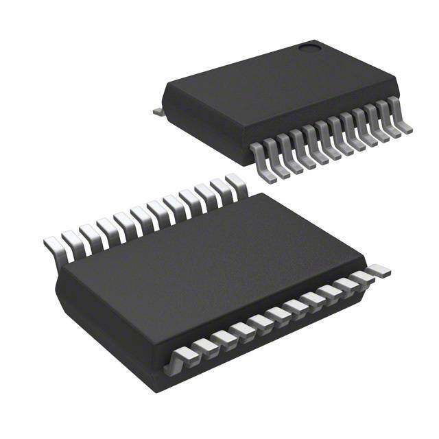
| 供应商器件封装 | 32-TQFP(7x7) |
| 其它名称 | ATMEGA64M1-15AZCT |
| 包装 | 剪切带 (CT) |
| 外设 | 欠压检测/复位,POR,PWM,温度传感器,WDT |
| 封装/外壳 | 32-TQFP |
| 工作温度 | -40°C ~ 125°C |
| 振荡器类型 | 内部 |
| 数据转换器 | A/D 11x10b; D/A 1x10b |
| 标准包装 | 1 |
| 核心处理器 | AVR |
| 核心尺寸 | 8-位 |
| 电压-电源(Vcc/Vdd) | 2.7 V ~ 5.5 V |
| 程序存储器类型 | 闪存 |
| 程序存储容量 | 64KB(32K x 16) |
| 连接性 | CAN,LIN,SPI,UART/USART |
| 速度 | 16MHz |


- 商务部:美国ITC正式对集成电路等产品启动337调查
- 曝三星4nm工艺存在良率问题 高通将骁龙8 Gen1或转产台积电
- 太阳诱电将投资9.5亿元在常州建新厂生产MLCC 预计2023年完工
- 英特尔发布欧洲新工厂建设计划 深化IDM 2.0 战略
- 台积电先进制程称霸业界 有大客户加持明年业绩稳了
- 达到5530亿美元!SIA预计今年全球半导体销售额将创下新高
- 英特尔拟将自动驾驶子公司Mobileye上市 估值或超500亿美元
- 三星加码芯片和SET,合并消费电子和移动部门,撤换高东真等 CEO
- 三星电子宣布重大人事变动 还合并消费电子和移动部门
- 海关总署:前11个月进口集成电路产品价值2.52万亿元 增长14.8%


PDF Datasheet 数据手册内容提取
ATmega16M1/ATmega32M1/ATmega64M1/ ATmega32C1/ATmega64C1 Automotive 8-bit AVR Microcontroller with 16K/32K/64Kbytes In-system DATASHEET Features ● High performance, low power AVR® 8-bit microcontroller ● Advanced RISC architecture ● 131 powerful instructions - most single clock cycle execution ● 32 x 8 general purpose working registers ● Fully static operation ● Up to 1MIPS throughput per MHz ● On-chip 2-cycle multiplier ● Data and non-volatile program memory ● 16K/32K/64Kbytes flash of in-system programmable program memory ● Endurance: 10,000 write/erase cycles ● Optional boot code section with independent lock bits ● In-system programming by on-chip boot program ● True read-while-write operation ● 512/1024/2048 Bytes of in-system programmable EEPROM ● Endurance: 100,000 write/erase cycles ● Programming lock for flash program and EEPROM data security ● 1024/2048/4096 bytes internal SRAM ● On chip debug interface (debugWIRE) ● CAN 2.0A/B with 6 message objects - ISO 16845 certified(1) ● LIN 2.1 and 1.3 controller or 8-Bit UART ● One 12-bit high-speed PSC (power stage controller) (only Atmel® ATmega16/32/64M1) ● Non overlapping inverted PWM output pins with flexible dead-time ● Variable PWM duty cycle and frequency ● Synchronous update of all PWM registers ● Auto stop function for emergency event ● Peripheral features ● One 8-bit general purpose Timer/Counter with separate prescaler, compare mode and capture mode ● One 16-bit general purpose Timer/Counter with separate prescaler, compare mode and capture mode ● One master/slave SPI serial interface 7647O-AVR-01/15
● 10-bit ADC ● Up to 11 single ended channels and 3 fully differential ADC channel pairs ● Programmable gain (5x, 10x, 20x, 40x) on differential channels ● Internal reference voltage ● Direct power supply voltage measurement ● 10-bit DAC for variable voltage reference (comparators, ADC) ● Four analog comparators with variable threshold detection ● 100µA ±6% current source (LIN node identification) ● Interrupt and wake-up on pin change ● Programmable watchdog timer with separate on-chip oscillator ● On-chip temperature sensor ● Special microcontroller features ● Low power idle, noise reduction, and power down modes ● Power on reset and programmable brown out detection ● In-system programmable via SPI port ● High precision crystal oscillator for CAN operations (16MHz) ● Internal calibrated RC oscillator (8MHz) ● On-chip PLL for fast PWM (32MHz, 64MHz) and CPU (16MHz) (only Atmel® ATmega16/32/64M1) ● Operating voltage: ● 2.7V - 5.5V ● Extended operating temperature: ● –40°C to +125°C ● Core speed grade: ● 0 - 8MHz at 2.7 - 4.5V ● 0 - 16MHz at 4.5 - 5.5V Note: 1. See certification on Atmel web site and note on Section 16.4.3 “Baud Rate” on page 148. Table 1. ATmega32/64/M1/C1 Product Line-up Part Number ATmega32C1 ATmega64C1 ATmega16M1 ATmega32M1 ATmega64M1 Flash size 32Kbyte 64Kbyte 16Kbyte 32Kbyte 64Kbyte RAM size 2048 bytes 4096 bytes 1024 bytes 2048 bytes 4096 bytes EEPROM size 1024 bytes 2048 bytes 512 bytes 1024 bytes 2048 bytes 8-bit timer Yes 16-bit timer Yes PSC No Yes PWM outputs 4 4 10 10 10 Fault inputs (PSC) 0 0 3 3 3 PLL No Yes 11 single 10-bit ADC channels 3 differential 10-bit DAC Yes analog comparators 4 Current source Yes CAN Yes LIN/UART Yes On-chip temp. Yes sensor SPI interface Yes 2 ATmega16/32/64/M1/C1 [DATASHEET] 7647O–AVR–01/15
1. Pin Configurations Figure 1-1. ATmega16/32/64M1 TQFP32/QFN32 (7*7mm) Package 5) T N 7) CI T P CINT17/PSCIN0/CLKO) CINT24/RESET/OCD) CINT8/INT3/PSCOUT1A) CINT16/PSCOUT0A) DC4/PSCOUT0B/SCK/PCIN DC7/PSCOUT1B/PCINT6) DC6/INT2/ACMPN1/AMP2-/ 2A/AMP2+/PCINT15) P P P P A A A D 1 ( 0 ( 0 ( 0 ( 7 ( 6 ( 5 ( 7 ( D E C D B B B C P P P P P P P P 32 31 30 29 28 27 26 25 (PCINT18/PSCIN2/OC1A/MISO_A) PD2 1 24 PB4 (AMP0+/PCINT4) (PCINT19/TXD/TXLIN/OC0A/MOSI_A) PD3 2 23 PB3 (AMP0-/PCINT3) (PCINT9/PSCIN1/OC1B/SS_A) PC1 3 22 PC6 (ADC10-/ACMP1/PCINT14) VCC 4 21 AREF(ISRC) GND 5 20 AGND (PCINT10/T0/TXCAN) PC2 6 19 AVCC (PCINT11/T1/RXCAN/ICP1B) PC3 7 18 PC5 (ADC9/ACMP3/AMP1+/PCINT13) (PCINT0/MISO/PSCOUT2A) PB0 8 17 PC4 (ADC8/ACMPN3/AMP1-/PCINT12) 9 10 11 12 13 14 15 16 1 1 2 4 5 6 7 2 B E E D D D D B P P P P P P P P B) 1) 2) A) 1) 2) 3) 2) T2 AL AL K_ T2 T2 T2 NT PCINT1/MOSI/PSCOU (PCINT25/OC0B/XT (PCINT26/ADC0/XT RXD/RXLIN/ICP1A/SC (ADC2/ACMP2/PCIN 3/ACMPN2/INT0/PCIN (ACMP0/PCIN C5/INT1/ACMPN0/PCI ( ADC1/ (ADC (AD 0/ 2 T N CI P ( Note: On the engineering samples (Parts marked AT90PWM324), the ACMPN3 alternate function is not located on PC4. It is located on PE2. ATmega16/32/64/M1/C1 [DATASHEET] 3 7647O–AVR–01/15
Figure 1-2. ATmega32/64C1 TQFP32/QFN32 (7*7 mm) Package 5) T N CI P 2-/ P M OCD) 7) N1/A T15) CINT17/CLKO) CINT24/RESET/ CINT8/INT3) CINT16) DC4/SCK/PCINT DC7/PCINT6) DC6/INT2/ACMP 2A/AMP2+/PCIN P P P P A A A D 1 ( 0 ( 0 ( 0 ( 7 ( 6 ( 5 ( 7 ( D E C D B B B C P P P P P P P P 32 31 30 29 28 27 26 25 (PCINT18/OC1A/MISO_A) PD2 1 24 PB4 (AMP0+/PCINT4) (PCINT19/TXD/TXLIN/OC0A/MOSI_A) PD3 2 23 PB3 (AMP0-/PCINT3) (PCINT9/OC1B/SS_A) PC1 3 22 PC6 (ADC10-/ACMP1/PCINT14) VCC 4 21 AREF(ISRC) GND 5 20 AGND (PCINT10/T0/TXCAN) PC2 6 19 AVCC (PCINT11/T1/RXCAN/ICP1B) PC3 7 18 PC5 (ADC9/ACMP3/AMP1+/PCINT13) (PCINT0/MISO) PB0 8 17 PC4 (ADC8/ACMPN3/AMP1-/PCINT12) 9 10 11 12 13 14 15 16 1 1 2 4 5 6 7 2 B E E D D D D B P P P P P P P P OSI) AL1) AL2) K_A) T21) T22) T23) NT2) (PCINT1/M CINT25/OC0B/XT CINT26/ADC0/XT RXLIN/ICP1A/SC C2/ACMP2/PCIN MPN2/INT0/PCIN (ACMP0/PCIN T1/ACMPN0/PCI (P (P RXD/ (AD 3/AC C5/IN ADC1/ (ADC (AD 0/ 2 T N CI P ( Note: On the first engineering samples (Parts marked AT90PWM324), the ACMPN3 alternate function is not located on PC4. It is located on PE2. 4 ATmega16/32/64/M1/C1 [DATASHEET] 7647O–AVR–01/15
1.1 Pin Descriptions Table 1-1. Pin Out Description QFN32 Pin Number Mnemonic Type Name, Function and Alternate Function 5 GND Power Ground: 0V reference 20 AGND Power Analog Ground: 0V reference for analog part 4 VCC Power Power Supply Analog Power Supply: This is the power supply voltage for analog 19 AVCC Power part For a normal use this pin must be connected. Analog Reference: reference for analog converter. This is the reference voltage of the A/D converter. As output, can be used by 21 AREF Power external analog ISRC (Current Source Output) MISO (SPI Master In Slave Out) 8 PB0 I/O PSCOUT2A (PSC Module 2 Output A) PCINT0 (Pin Change Interrupt 0) MOSI (SPI Master Out Slave In) 9 PB1 I/O PSCOUT2B (PSC Module 2 Output B) PCINT1 (Pin Change Interrupt 1) ADC5 (Analog Input Channel 5 ) INT1 (External Interrupt 1 Input) 16 PB2 I/O ACMPN0 (analog comparator 0 Negative Input) PCINT2 (Pin Change Interrupt 2) AMP0- (Analog Differential Amplifier 0 Negative Input) 23 PB3 I/O PCINT3 (Pin Change Interrupt 3) AMP0+ (Analog Differential Amplifier 0 Positive Input) 24 PB4 I/O PCINT4 (Pin Change Interrupt 4) ADC6 (Analog Input Channel 6) INT2 (External Interrupt 2 Input) 26 PB5 I/O ACMPN1 (analog comparator 1 Negative Input) AMP2- (Analog Differential Amplifier 2 Negative Input) PCINT5 (Pin Change Interrupt 5) ADC7 (Analog Input Channel 7) 27 PB6 I/O PSCOUT1B (PSC Module 1 Output A) PCINT6 (Pin Change Interrupt 6) ADC4 (Analog Input Channel 4) PSCOUT0B (PSC Module 0 Output B) 28 PB7 I/O SCK (SPI Clock) PCINT7 (Pin Change Interrupt 7) PSCOUT1A (PSC Module 1 Output A) 30 PC0 I/O INT3 (External Interrupt 3 Input) PCINT8 (Pin Change Interrupt 8) Note: 1. On the first engineering samples (Parts marked AT90PWM324), the ACMPN3 alternate function is not located on PC4. It is located on PE2. ATmega16/32/64/M1/C1 [DATASHEET] 5 7647O–AVR–01/15
Table 1-1. Pin Out Description (Continued) QFN32 Pin Number Mnemonic Type Name, Function and Alternate Function PSCIN1 (PSC Digital Input 1) OC1B (Timer 1 Output Compare B) 3 PC1 I/O SS_A (Alternate SPI Slave Select) PCINT9 (Pin Change Interrupt 9) T0 (Timer 0 clock input) 6 PC2 I/O TXCAN (CAN Transmit Output) PCINT10 (Pin Change Interrupt 10) T1 (Timer 1 clock input) RXCAN (CAN Receive Input) 7 PC3 I/O ICP1B (Timer 1 input capture alternate B input) PCINT11 (Pin Change Interrupt 11) ADC8 (Analog Input Channel 8) AMP1- (Analog Differential Amplifier 1 Negative Input) 17 PC4 I/O ACMPN3 (analog comparator 3 Negative Input) PCINT12 (Pin Change Interrupt 12) ADC9 (Analog Input Channel 9) AMP1+ (Analog Differential Amplifier 1 Positive Input) 18 PC5 I/O ACMP3 (analog comparator 3 Positive Input) PCINT13 (Pin Change Interrupt 13) ADC10 (Analog Input Channel 10) 22 PC6 I/O ACMP1 (analog comparator 1 Positive Input) PCINT14 (Pin Change Interrupt 14) D2A (DAC output) 25 PC7 I/O AMP2+ (Analog Differential Amplifier 2 Positive Input) PCINT15 (Pin Change Interrupt 15) PSCOUT0A (PSC Module 0 Output A) 29 PD0 I/O PCINT16 (Pin Change Interrupt 16) PSCIN0 (PSC Digital Input 0) 32 PD1 I/O CLKO (System Clock Output) PCINT17 (Pin Change Interrupt 17) OC1A (Timer 1 Output Compare A) PSCIN2 (PSC Digital Input 2) 1 PD2 I/O MISO_A (Programming and alternate SPI Master In Slave Out) PCINT18 (Pin Change Interrupt 18) TXD (UART Tx data) TXLIN (LIN Transmit Output) OC0A (Timer 0 Output Compare A) 2 PD3 I/O SS (SPI Slave Select) MOSI_A (Programming and alternate Master Out SPI Slave In) PCINT19 (Pin Change Interrupt 19) Note: 1. On the first engineering samples (Parts marked AT90PWM324), the ACMPN3 alternate function is not located on PC4. It is located on PE2. 6 ATmega16/32/64/M1/C1 [DATASHEET] 7647O–AVR–01/15
Table 1-1. Pin Out Description (Continued) QFN32 Pin Number Mnemonic Type Name, Function and Alternate Function ADC1 (Analog Input Channel 1) RXD (UART Rx data) RXLIN (LIN Receive Input) 12 PD4 I/O ICP1A (Timer 1 input capture alternate A input) SCK_A (Programming and alternate SPI Clock) PCINT20 (Pin Change Interrupt 20) ADC2 (Analog Input Channel 2) 13 PD5 I/O ACMP2 (analog comparator 2 Positive Input) PCINT21 (Pin Change Interrupt 21) ADC3 (Analog Input Channel 3) ACMPN2 (analog comparator 2 Negative Input) 14 PD6 I/O INT0 (External Interrupt 0 Input) PCINT22 (Pin Change Interrupt 22) ACMP0 (analog comparator 0 Positive Input) 15 PD7 I/O PCINT23 (Pin Change Interrupt 23) RESET (Reset Input) 31 PE0 I/O or I OCD (On Chip Debug I/O) PCINT24 (Pin Change Interrupt 24) XTAL1 (XTAL Input) 10 PE1 I/O OC0B (Timer 0 Output Compare B) PCINT25 (Pin Change Interrupt 25) XTAL2 (XTAL Output) 11 PE2 I/O ADC0 (Analog Input Channel 0) PCINT26 (Pin Change Interrupt 26) Note: 1. On the first engineering samples (Parts marked AT90PWM324), the ACMPN3 alternate function is not located on PC4. It is located on PE2. ATmega16/32/64/M1/C1 [DATASHEET] 7 7647O–AVR–01/15
2. Overview The Atmel® ATmega16/32/64/M1/C1 is a low-power CMOS 8-bit microcontroller based on the AVR® enhanced RISC architecture. By executing powerful instructions in a single clock cycle, the Atmel ATmega16/32/64/M1/C1 achieves throughputs approaching 1MIPS per MHz allowing the system designer to optimize power consumption versus processing speed. 2.1 Block Diagram Figure 2-1. Block Diagram Data Bus 8-bit Flash Program Status and Interrupt Program Counter Control Unit Memory SPI Unit 32 x 8 General Instruction Purpose Watchdog Register Registers Timer 4 Analog g Instruction g n Comparators Decoder ddressin Addressi ALU HW LIN/UART Control Lines Direct A ndirect I Timer 0 Data Timer 1 SRAM ADC EEPROM DAC I/O Lines MPSC Current Source CAN The AVR core combines a rich instruction set with 32 general purpose working registers. All the 32 registers are directly connected to the Arithmetic Logic Unit (ALU), allowing two independent registers to be accessed in one single instruction executed in one clock cycle. The resulting architecture is more code efficient while achieving throughputs up to ten times faster than conventional CISC microcontrollers. The Atmel ATmega16/32/64/M1/C1 provides the following features: 16K/32K/64K bytes of In-System Programmable Flash with Read-while-write capabilities, 512/1024/2048 bytes EEPROM, 1024/2048/4096 bytes SRAM, 27 general purpose I/O lines, 32 general purpose working registers, one Motor Power Stage Controller, two flexible Timer/Counters with compare modes and PWM, one UART with HW LIN, an 11-channel 10-bit ADC with two differential input stages with programmable gain, a 10-bit DAC, a programmable Watchdog Timer with Internal Individual Oscillator, an SPI serial port, an On-chip Debug system and four software selectable power saving modes. 8 ATmega16/32/64/M1/C1 [DATASHEET] 7647O–AVR–01/15
The Idle mode stops the CPU while allowing the SRAM, Timer/Counters, SPI ports, CAN, LIN/UART and interrupt system to continue functioning. The Power-down mode saves the register contents but freezes the Oscillator, disabling all other chip functions until the next interrupt or Hardware Reset. The ADC noise reduction mode stops the CPU and all I/O modules except ADC, to minimize switching noise during ADC conversions. In Standby mode, the Crystal/Resonator Oscillator is running while the rest of the device is sleeping. This allows very fast start-up combined with low power consumption. The device is manufactured using Atmel’s high-density nonvolatile memory technology. The On-chip ISP Flash allows the program memory to be reprogrammed in-system through an SPI serial interface, by a conventional nonvolatile memory programmer, or by an On-chip Boot program running on the AVR core. The boot program can use any interface to download the application program in the application Flash memory. Software in the boot flash section will continue to run while the application flash section is updated, providing true read-while-write operation. By combining an 8-bit RISC CPU with in- system self-programmable flash on a monolithic chip, the Atmel ATmega16/32/64/M1/C1 is a powerful microcontroller that provides a highly flexible and cost effective solution to many embedded control applications. The ATmega16/32/64/M1/C1 AVR is supported with a full suite of program and system development tools including: C compilers, macro assemblers, program debugger/simulators, in-circuit emulators, and evaluation kits. 2.2 Automotive Quality Grade The Atmel® ATmega16/32/64/M1/C1 have been developed and manufactured according to the most stringent requirements of the international standard ISO-TS-16949. This data sheet contains limit values extracted from the results of extensive characterization (Temperature and Voltage). The quality and reliability of the ATmega16/32/64/M1/C1 have been verified during regular product qualification as per AEC-Q100 grade 1. As indicated in the ordering information paragraph, the products are available in only one temperature grade. Table 2-1. Temperature Grade Identification for Automotive Products Temperature Temperature Identifier Comments –40, +125 Z Full automotive temperature range 2.3 Pin Descriptions 2.3.1 VCC Digital supply voltage. 2.3.2 GND Ground. 2.3.3 Port B (PB7..PB0) Port B is an 8-bit bi-directional I/O port with internal pull-up resistors (selected for each bit). The Port B output buffers have symmetrical drive characteristics with both high sink and source capability. As inputs, Port B pins that are externally pulled low will source current if the pull-up resistors are activated. The Port B pins are tri-stated when a reset condition becomes active, even if the clock is not running. Port B also serves the functions of various special features of the Atmel ATmega16/32/64/M1/C1 as listed in Section 9.3.2 “Alternate Functions of Port B” on page 58. 2.3.4 Port C (PC7..PC0) Port C is an 8-bit bi-directional I/O port with internal pull-up resistors (selected for each bit). The Port C output buffers have symmetrical drive characteristics with both high sink and source capability. As inputs, Port C pins that are externally pulled low will source current if the pull-up resistors are activated. The Port C pins are tri-stated when a reset condition becomes active, even if the clock is not running. Port C also serves the functions of special features of the ATmega16/32/64/M1/C1 as listed in Section 9.3.3 “Alternate Functions of Port C” on page 61. ATmega16/32/64/M1/C1 [DATASHEET] 9 7647O–AVR–01/15
2.3.5 Port D (PD7..PD0) Port D is an 8-bit bi-directional I/O port with internal pull-up resistors (selected for each bit). The port D output buffers have symmetrical drive characteristics with both high sink and source capability. As inputs, port D pins that are externally pulled low will source current if the pull-up resistors are activated. The port D pins are tri-stated when a reset condition becomes active, even if the clock is not running. Port D also serves the functions of various special features of the Atmel® ATmega16/32/64/M1/C1 as listed on 64. 2.3.6 Port E (PE2..0) RESET/ XTAL1/ XTAL2 Port E is an 3-bit bi-directional I/O port with internal pull-up resistors (selected for each bit). The port E output buffers have symmetrical drive characteristics with both high sink and source capability. As inputs, port E pins that are externally pulled low will source current if the pull-up resistors are activated. The Port E pins are tri-stated when a reset condition becomes active, even if the clock is not running. If the RSTDISBL fuse is programmed, PE0 is used as an I/O pin. Note that the electrical characteristics of PE0 differ from those of the other pins of Port E. If the RSTDISBL fuse is unprogrammed, PE0 is used as a Reset input. A low level on this pin for longer than the minimum pulse length will generate a Reset, even if the clock is not running. The minimum pulse length is given in Table 7-1 on page 39. Shorter pulses are not guaranteed to generate a reset. Depending on the clock selection fuse settings, PE1 can be used as input to the inverting oscillator amplifier and input to the internal clock operating circuit. Depending on the clock selection fuse settings, PE2 can be used as output from the inverting oscillator amplifier. The various special features of Port E are elaborated in Section 9.3.5 “Alternate Functions of Port E” on page 67 and Section 5.1 “Clock Systems and their Distribution” on page 25. 2.3.7 AVCC AVCC is the supply voltage pin for the A/D converter, D/A converter, current source. It should be externally connected to V , even if the ADC, DAC are not used. If the ADC is used, it should be connected to V through a low-pass filter (see CC CC Section 18.6.2 “Analog Noise Canceling Techniques” on page 204). 2.3.8 AREF This is the analog reference pin for the A/D converter. 2.4 About Code Examples This documentation contains simple code examples that briefly show how to use various parts of the device. These code examples assume that the part specific header file is included before compilation. Be aware that not all C compiler vendors include bit definitions in the header files and interrupt handling in C is compiler dependent. Please confirm with the C compiler documentation for more details. 10 ATmega16/32/64/M1/C1 [DATASHEET] 7647O–AVR–01/15
3. AVR CPU Core 3.1 Introduction This section discusses the AVR® core architecture in general. The main function of the CPU core is to ensure correct program execution. The CPU must therefore be able to access memories, perform calculations, control peripherals, and handle interrupts. 3.2 Architectural Overview Figure 3-1. Block Diagram of the AVR Architecture Data Bus 8-bit Flash Program Status and Program Counter Control Memory Interrupt 32 x 8 Unit General Instruction Purpose Register Registers SPI Unit g Instruction g n Decoder dressin ddressi ALU WaTticmhedrog d A Control Lines Direct A ndirect CoAmnpaaloragtor I I/O Module 1 Data SRAM I/O Module 2 I/O Module n EEPROM I/O Lines In order to maximize performance and parallelism, the AVR uses a Harvard architecture – with separate memories and buses for program and data. Instructions in the program memory are executed with a single level pipelining. While one instruction is being executed, the next instruction is pre-fetched from the program memory. This concept enables instructions to be executed in every clock cycle. The program memory is in-system reprogrammable Flash memory. The fast-access register file contains 32 x 8-bit general purpose working registers with a single clock cycle access time. This allows single-cycle arithmetic logic unit (ALU) operation. In a typical ALU operation, two operands are output from the register file, the operation is executed, and the result is stored back in the register file – in one clock cycle. ATmega16/32/64/M1/C1 [DATASHEET] 11 7647O–AVR–01/15
Six of the 32 registers can be used as three 16-bit indirect address register pointers for data space addressing – enabling efficient address calculations. One of the these address pointers can also be used as an address pointer for look up tables in Flash program memory. These added function registers are the 16-bit X-, Y-, and Z-register, described later in this section. The ALU supports arithmetic and logic operations between registers or between a constant and a register. Single register operations can also be executed in the ALU. After an arithmetic operation, the Status Register is updated to reflect information about the result of the operation. Program flow is provided by conditional and unconditional jump and call instructions, able to directly address the whole address space. Most AVR instructions have a single 16-bit word format. Every program memory address contains a 16- or 32-bit instruction. Program flash memory space is divided in two sections, the boot program section and the application program section. Both sections have dedicated Lock bits for write and read/write protection. The SPM (store program memory) instruction that writes into the application flash memory section must reside in the boot program section. during interrupts and subroutine calls, the return address program counter (PC) is stored on the stack. The stack is effectively allocated in the general data SRAM, and consequently the stack size is only limited by the total SRAM size and the usage of the SRAM. All user programs must initialize the SP in the reset routine (before subroutines or interrupts are executed). The stack pointer (SP) is read/write accessible in the I/O space. The data SRAM can easily be accessed through the five different addressing modes supported in the AVR architecture. The memory spaces in the AVR® architecture are all linear and regular memory maps. A flexible interrupt module has its control registers in the I/O space with an additional global interrupt enable bit in the status register. All interrupts have a separate interrupt vector in the interrupt vector table. The interrupts have priority in accordance with their interrupt vector position. The lower the interrupt vector address, the higher is the priority. The I/O memory space contains 64 addresses for CPU peripheral functions as control registers, SPI, and other I/O functions. The I/O memory can be accessed directly, or as the data space locations following those of the register file, 0x20 - 0x5F. In addition, the Atmel ATmega16/32/64/M1/C1 has extended I/O space from 0x60 - 0xFF in SRAM where only the ST/STS/STD and LD/LDS/LDD instructions can be used. 3.3 ALU – Arithmetic Logic Unit The high-performance AVR ALU operates in direct connection with all the 32 general purpose working registers. Within a single clock cycle, arithmetic operations between general purpose registers or between a register and an immediate are executed. The ALU operations are divided into three main categories – arithmetic, logical, and bit-functions. Some implementations of the architecture also provide a powerful multiplier supporting both signed/unsigned multiplication and fractional format. See the “Instruction Set” section for a detailed description. 3.4 Status Register The status register contains information about the result of the most recently executed arithmetic instruction. This information can be used for altering program flow in order to perform conditional operations. Note that the status register is updated after all ALU operations, as specified in the Instruction Set Reference. This will in many cases remove the need for using the dedicated compare instructions, resulting in faster and more compact code. The status register is not automatically stored when entering an interrupt routine and restored when returning from an interrupt. This must be handled by software. The AVR Status Register – SREG – is defined as: Bit 7 6 5 4 3 2 1 0 I T H S V N Z C SREG Read/Write R/W R/W R/W R/W R/W R/W R/W R/W Initial Value 0 0 0 0 0 0 0 0 • Bit 7 – I: Global Interrupt Enable The global interrupt enable bit must be set to enabled the interrupts. The individual interrupt enable control is then performed in separate control registers. If the global interrupt enable register is cleared, none of the interrupts are enabled independent of the individual interrupt enable settings. The I-bit is cleared by hardware after an interrupt has occurred, and is set by the RETI instruction to enable subsequent interrupts. The I-bit can also be set and cleared by the application with the SEI and CLI instructions, as described in the instruction set reference. 12 ATmega16/32/64/M1/C1 [DATASHEET] 7647O–AVR–01/15
• Bit 6 – T: Bit Copy Storage The bit copy instructions BLD (Bit LoaD) and BST (Bit STore) use the T-bit as source or destination for the operated bit. A bit from a register in the register file can be copied into T by the BST instruction, and a bit in T can be copied into a bit in a register in the register file by the BLD instruction. • Bit 5 – H: Half Carry Flag The half carry flag H indicates a half carry in some arithmetic operations. Half carry Is useful in BCD arithmetic. See the “Instruction Set Description” for detailed information. • Bit 4 – S: Sign Bit, S = N V The S-bit is always an exclusive or between the negative flag N and the two’s complement overflow flag V. See the “Instruction Set Description” for detailed information. • Bit 3 – V: Two’s Complement Overflow Flag The two’s complement overflow flag V supports two’s complement arithmetics. See the “Instruction Set Description” for detailed information. • Bit 2 – N: Negative Flag The negative flag N indicates a negative result in an arithmetic or logic operation. See the “Instruction Set Description” for detailed information. • Bit 1 – Z: Zero Flag The zero flag Z indicates a zero result in an arithmetic or logic operation. See the “Instruction Set Description” for detailed information. • Bit 0 – C: Carry Flag The carry flag C indicates a carry in an arithmetic or logic operation. See the “Instruction Set Description” for detailed information. 3.5 General Purpose Register File The register file is optimized for the AVR enhanced RISC instruction set. In order to achieve the required performance and flexibility, the following input/output schemes are supported by the register file: ● One 8-bit output operand and one 8-bit result input ● Two 8-bit output operands and one 8-bit result input ● Two 8-bit output operands and one 16-bit result input ● One 16-bit output operand and one 16-bit result input ATmega16/32/64/M1/C1 [DATASHEET] 13 7647O–AVR–01/15
Figure 3-2 shows the structure of the 32 general purpose working registers in the CPU. Figure 3-2. AVR CPU General Purpose Working Registers 7 0 Addr. R0 0x00 R1 0x01 R2 0x02 … R13 0x0D General R14 0x0E Purpose R15 0x0F Working R16 0x10 Registers R17 0x11 … R26 0x1A X-register Low Byte R27 0x1B X-register High Byte R28 0x1C Y-register Low Byte R29 0x1D Y-register High Byte R30 0x1E Z-register Low Byte R31 0x1F Z-register High Byte Most of the instructions operating on the register file have direct access to all registers, and most of them are single cycle instructions. As shown in Figure 3-2, each register is also assigned a data memory address, mapping them directly into the first 32 locations of the user data space. Although not being physically implemented as SRAM locations, this memory organization provides great flexibility in access of the registers, as the X-, Y- and Z-pointer registers can be set to index any register in the file. 3.5.1 The X-register, Y-register, and Z-register The registers R26..R31 have some added functions to their general purpose usage. These registers are 16-bit address pointers for indirect addressing of the data space. The three indirect address registers X, Y, and Z are defined as described in Figure 3-3. Figure 3-3. The X-, Y-, and Z-registers 15 XH XL 0 X-register 7 0 7 0 R27 (0x1B) R26 (0x1A) 15 YH YL 0 Y-register 7 0 7 0 R29 (0x1D) R28 (0x1C) 15 ZH ZL 0 Z-register 7 0 7 0 R31 (0x1F) R30 (0x1E) In the different addressing modes these address registers have functions as fixed displacement, automatic increment, and automatic decrement (see the instruction set reference for details). 14 ATmega16/32/64/M1/C1 [DATASHEET] 7647O–AVR–01/15
3.6 Stack Pointer The stack is mainly used for storing temporary data, for storing local variables and for storing return addresses after interrupts and subroutine calls. The stack pointer register always points to the top of the stack. Note that the stack is implemented as growing from higher memory locations to lower memory locations. This implies that a Stack PUSH command decreases the stack pointer. The stack pointer points to the data SRAM stack area where the subroutine and interrupt stacks are located. This stack space in the data SRAM must be defined by the program before any subroutine calls are executed or interrupts are enabled. The stack pointer must be set to point above 0x100. The stack pointer is decremented by one when data is pushed onto the stack with the PUSH instruction, and it is decremented by two when the return address is pushed onto the stack with subroutine call or interrupt. The stack pointer is incremented by one when data is popped from the stack with the POP instruction, and it is incremented by two when data is popped from the stack with return from subroutine RET or return from interrupt RETI. The AVR® stack pointer is implemented as two 8-bit registers in the I/O space. The number of bits actually used is implementation dependent. Note that the data space in some implementations of the AVR architecture is so small that only SPL is needed. In this case, the SPH Register will not be present. Bit 15 14 13 12 11 10 9 8 SP15 SP14 SP13 SP12 SP11 SP10 SP9 SP8 SPH SP7 SP6 SP5 SP4 SP3 SP2 SP1 SP0 SPL 7 6 5 4 3 2 1 0 Read/Write R/W R/W R/W R/W R/W R/W R/W R/W R/W R/W R/W R/W R/W R/W R/W R/W Initial Value Top address of the SRAM (0x04FF/0x08FF/0x10FF) 3.7 Instruction Execution Timing This section describes the general access timing concepts for instruction execution. The AVR CPU is driven by the CPU clock clk , directly generated from the selected clock source for the chip. No internal clock division is used. CPU Figure 3-4 shows the parallel instruction fetches and instruction executions enabled by the Harvard architecture and the fast- access Register File concept. This is the basic pipelining concept to obtain up to 1 MIPS per MHz with the corresponding unique results for functions per cost, functions per clocks, and functions per power-unit. Figure 3-4. The Parallel Instruction Fetches and Instruction Executions T1 T2 T3 T4 clk CPU 1st Instruction Fetch 1st Instruction Execute 2nd Instruction Fetch 2nd Instruction Execute 3rd Instruction Fetch 3rd Instruction Execute 4th Instruction Fetch ATmega16/32/64/M1/C1 [DATASHEET] 15 7647O–AVR–01/15
Figure 3-5 shows the internal timing concept for the Register File. In a single clock cycle an ALU operation using two register operands is executed, and the result is stored back to the destination register. Figure 3-5. Single Cycle ALU Operation T1 T2 T3 T4 clk CPU Total Execution Time Register Operands Fetch ALU Operation Execute Result Write Back 3.8 Reset and Interrupt Handling The AVR® provides several different interrupt sources. These interrupts and the separate reset vector each have a separate program vector in the program memory space. All interrupts are assigned individual enable bits which must be written logic one together with the global interrupt enable bit in the status register in order to enable the interrupt. Depending on the program counter value, interrupts may be automatically disabled when boot lock bits BLB02 or BLB12 are programmed. This feature improves software security. See Section 25. “Memory Programming” on page 255 for details. The lowest addresses in the program memory space are by default defined as the reset and interrupt vectors. The complete list of vectors is shown in Section 8. “Interrupts” on page 47. The list also determines the priority levels of the different interrupts. The lower the address the higher is the priority level. RESET has the highest priority, and next is ANACOMP0 – the analog comparator 0 interrupt. The interrupt vectors can be moved to the start of the boot flash section by setting the IVSEL bit in the MCU control register (MCUCR). Refer to Section 8. “Interrupts” on page 47 for more information. The reset vector can also be moved to the start of the boot flash section by programming the BOOTRST fuse, see Section 24. “Boot Loader Support – Read-while-write Self-Programming ATmega16/32/64/M1/C1” on page 241. 3.8.1 Interrupt Behavior When an interrupt occurs, the global interrupt enable I-bit is cleared and all interrupts are disabled. The user software can write logic one to the I-bit to enable nested interrupts. All enabled interrupts can then interrupt the current interrupt routine. The I-bit is automatically set when a return from interrupt instruction – RETI – is executed. There are basically two types of interrupts. The first type is triggered by an event that sets the interrupt flag. For these interrupts, the program counter is vectored to the actual interrupt vector in order to execute the interrupt handling routine, and hardware clears the corresponding interrupt flag. Interrupt flags can also be cleared by writing a logic one to the flag bit position(s) to be cleared. If an interrupt condition occurs while the corresponding interrupt enable bit is cleared, the interrupt flag will be set and remembered until the interrupt is enabled, or the flag is cleared by software. Similarly, if one or more interrupt conditions occur while the global interrupt enable bit is cleared, the corresponding interrupt flag(s) will be set and remembered until the global interrupt enable bit is set, and will then be executed by order of priority. The second type of interrupts will trigger as long as the interrupt condition is present. These interrupts do not necessarily have interrupt flags. If the interrupt condition disappears before the interrupt is enabled, the interrupt will not be triggered. When the AVR exits from an interrupt, it will always return to the main program and execute one more instruction before any pending interrupt is served. Note that the status register is not automatically stored when entering an interrupt routine, nor restored when returning from an interrupt routine. This must be handled by software. When using the CLI instruction to disable interrupts, the interrupts will be immediately disabled. No interrupt will be executed after the CLI instruction, even if it occurs simultaneously with the CLI instruction. The following example shows how this can be used to avoid interrupts during the timed EEPROM write sequence. 16 ATmega16/32/64/M1/C1 [DATASHEET] 7647O–AVR–01/15
Assembly Code Example in r16, SREG ; store SREG value cli ; disable interrupts during timed sequence sbi EECR, EEMWE ; start EEPROM write sbi EECR, EEWE out SREG, r16 ; restore SREG value (I-bit) C Code Example char cSREG; cSREG = SREG; /* store SREG value */ /* disable interrupts during timed sequence */ _CLI(); EECR |= (1<<EEMWE); /* start EEPROM write */ EECR |= (1<<EEWE); SREG = cSREG; /* restore SREG value (I-bit) */ When using the SEI instruction to enable interrupts, the instruction following SEI will be executed before any pending interrupts, as shown in this example. Assembly Code Example sei ; set Global Interrupt Enable sleep ; enter sleep, waiting for interrupt ; note: will enter sleep before any pending ; interrupt(s) C Code Example _SEI(); /* set Global Interrupt Enable */ _SLEEP(); /* enter sleep, waiting for interrupt */ /* note: will enter sleep before any pending interrupt(s) */ 3.8.2 Interrupt Response Time The interrupt execution response for all the enabled AVR® interrupts is four clock cycles minimum. After four clock cycles the program vector address for the actual interrupt handling routine is executed. during this four clock cycle period, the program counter is pushed onto the stack. The vector is normally a jump to the interrupt routine, and this jump takes three clock cycles. If an interrupt occurs during execution of a multi-cycle instruction, this instruction is completed before the interrupt is served. If an interrupt occurs when the MCU is in sleep mode, the interrupt execution response time is increased by four clock cycles. This increase comes in addition to the start-up time from the selected sleep mode. A return from an interrupt handling routine takes four clock cycles. during these four clock cycles, the program counter (two bytes) is popped back from the stack, the stack pointer is incremented by two, and the I-bit in SREG is set. ATmega16/32/64/M1/C1 [DATASHEET] 17 7647O–AVR–01/15
4. Memories This section describes the different memories in the Atmel® ATmega16/32/64/M1/C1. The AVR architecture has two main memory spaces, the data memory and the program memory space. In addition, the Atmel ATmega16/32/64/M1/C1 features an EEPROM Memory for data storage. All three memory spaces are linear and regular. 4.1 In-system Reprogrammable Flash Program Memory The Atmel ATmega16/32/64/M1/C1 contains 16K/32K/64K bytes on-chip in-system reprogrammable flash memory for program storage. Since all AVR® instructions are 16 or 32 bits wide, the Flash is organized as 8K x 16, 16K x 16 , 32K x 16. For software security, the flash program memory space is divided into two sections, boot program section and application program section. The flash memory has an endurance of at least 10,000 write/erase cycles. The Atmel ATmega16/32/64/M1/C1 program counter (PC) is 14/15 bits wide, thus addressing the 8K/16K/32K program memory locations. The operation of boot program section and associated boot lock bits for software protection are described in detail in Section 24. “Boot Loader Support – Read-while-write Self-Programming ATmega16/32/64/M1/C1” on page 241. Section 25. “Memory Programming” on page 255 contains a detailed description on flash programming in SPI or parallel programming mode. Constant tables can be allocated within the entire program memory address space (see the LPM – Load Program Memory. Timing diagrams for instruction fetch and execution are presented in Section 3.7 “Instruction Execution Timing” on page 15. Figure 4-1. Program Memory Map Program Memory 0x0000 Application Flash Section Boot Flash Section 0x1FFF/0x3FFF/0x7F 4.2 SRAM Data Memory Figure 4-2 shows how the Atmel ATmega16/32/64/M1/C1 SRAM memory is organized. The Atmel ATmega16/32/64/M1/C1 is a complex microcontroller with more peripheral units than can be supported within the 64 locations reserved in the Opcode for the IN and OUT instructions. For the extended I/O space from 0x60 - 0xFF in SRAM, only the ST/STS/STD and LD/LDS/LDD instructions can be used. The lower 2304 data memory locations address both the register File, the I/O memory, extended I/O memory, and the internal data SRAM. The first 32 locations address the register file, the next 64 location the standard I/O memory, then 160 locations of extended I/O memory, and the next 1024/2048/4096 locations address the internal data SRAM. The five different addressing modes for the data memory cover: Direct, Indirect with Displacement, Indirect, Indirect with Pre- decrement, and Indirect with Post-increment. In the register File, registers R26 to R31 feature the indirect addressing pointer registers. 18 ATmega16/32/64/M1/C1 [DATASHEET] 7647O–AVR–01/15
The direct addressing reaches the entire data space. The Indirect with Displacement mode reaches 63 address locations from the base address given by the Y- or Z-register. When using register indirect addressing modes with automatic pre-decrement and post-increment, the address registers X, Y, and Z are decremented or incremented. The 32 general purpose working registers, 64 I/O registers, 160 extended I/O registers, and the 1024/2048/4096 bytes of internal data SRAM in the Atmel® ATmega16/32/64/M1/C1 are all accessible through all these addressing modes. The register file is described in Section 3.5 “General Purpose Register File” on page 13. Figure 4-2. Data Memory Map for 1024/2048/4096 Internal SRAM Data Memory 32 Registers 0x0000 - 0x001F 64 I/O Registers 0x0020 - 0x005F 160 Ext I/O Registers 0x0060 - 0x00FF Internal SRAM 0x0100 (1024x8) (2048x8) 0x04FF/0x08FF/0x10FF (4096x8) 4.2.1 SRAM Data Access Times This section describes the general access timing concepts for internal memory access. Theinternal data SRAM access is performed in two clk cycles as described in Figure 4-3 on page 19. CPU Figure 4-3. On-chip Data SRAM Access Cycles T1 T2 T3 clk CPU Address Compute Address Address valid Data Write WR Data Read RD Memory Access Instruction Next Instruction ATmega16/32/64/M1/C1 [DATASHEET] 19 7647O–AVR–01/15
4.3 EEPROM Data Memory The Atmel® ATmega16/32/64/M1/C1 contains 512/1024/2048 bytes of data EEPROM memory. It is organized as a separate data space, in which single bytes can be read and written. The EEPROM has an endurance of at least 100,000 write/erase cycles. The access between the EEPROM and the CPU is described in the following, specifying the EEPROM Address Registers, the EEPROM Data Register, and the EEPROM Control Register. For a detailed description of SPI and Parallel data downloading to the EEPROM, see Section 25.9 “Serial Downloading” on page 270, and Section 25.6 “Parallel Programming Parameters, Pin Mapping, and Commands” on page 259 respectively. 4.3.1 EEPROM Read/Write Access The EEPROM Access Registers are accessible in the I/O space. The write access time for the EEPROM is given in Table 4-2. A self-timing function, however, lets the user software detect when the next byte can be written. If the user code contains instructions that write the EEPROM, some precautions must be taken. In heavily filtered power supplies, V is likely to rise or fall slowly on power-up/down. This causes the device for CC some period of time to run at a voltage lower than specified as minimum for the clock frequency used. Section 4.3.5 “Preventing EEPROM Corruption” on page 23 for details on how to avoid problems in these situations. In order to prevent unintentional EEPROM writes, a specific write procedure must be followed. Refer to the description of the EEPROM Control Register for details on this. When the EEPROM is read, the CPU is halted for four clock cycles before the next instruction is executed. When the EEPROM is written, the CPU is halted for two clock cycles before the next instruction is executed. 4.3.2 The EEPROM Address Registers – EEARH and EEARL Bit 15 14 13 12 11 10 9 8 – – – – – EEAR10 EEAR9 EEAR8 EEARH EEAR7 EEAR6 EEAR5 EEAR4 EEAR3 EEAR2 EEAR1 EEAR0 EEARL 7 6 5 4 3 2 1 0 Read/Write R R R R R R/W R/W R/W R/W R/W R/W R/W R/W R/W R/W R/W Initial Value 0 0 0 0 0 X X X X X X X X X X X • Bits 15.11 – Reserved Bits These bits are reserved bits in the ATmega16/32/64/M1/C1 and will always read as zero. • Bits 9..0 – EEAR10..0: EEPROM Address The EEPROM address registers – EEARH and EEARL specify the EEPROM address in the 512/1024/2048 bytes EEPROM space. The EEPROM data bytes are addressed linearly between 0 and 511/1023/2047. The initial value of EEAR is undefined. A proper value must be written before the EEPROM may be accessed. 4.3.3 The EEPROM Data Register – EEDR Bit 7 6 5 4 3 2 1 0 EEDR7 EEDR6 EEDR5 EEDR4 EEDR3 EEDR2 EEDR1 EEDR0 EEDR Read/Write R/W R/W R/W R/W R/W R/W R/W R/W Initial Value 0 0 0 0 0 0 0 0 • Bits 7..0 – EEDR7.0: EEPROM Data For the EEPROM write operation, the EEDR register contains the data to be written to the EEPROM in the address given by the EEAR register. For the EEPROM read operation, the EEDR contains the data read out from the EEPROM at the address given by EEAR. 20 ATmega16/32/64/M1/C1 [DATASHEET] 7647O–AVR–01/15
4.3.4 The EEPROM Control Register – EECR Bit 7 6 5 4 3 2 1 0 – – EEPM1 EEPM0 EERIE EEMWE EEWE EERE EECR Read/Write R R R/W R/W R/W R/W R/W R/W Initial Value 0 0 X X 0 0 X 0 • Bits 7..6 – Reserved Bits These bits are reserved bits in the ATmega16/32/64/M1/C1 and will always read as zero. • Bits 5..4 – EEPM1 and EEPM0: EEPROM Programming Mode Bits The EEPROM Programming mode bit setting defines which programming action that will be triggered when writing EEWE. It is possible to program data in one atomic operation (erase the old value and program the new value) or to split the Erase and Write operations in two different operations. The Programming times for the different modes are shown in Table 4-1. While EEWE is set, any write to EEPMn will be ignored. during reset, the EEPMn bits will be reset to 0b00 unless the EEPROM is busy programming. Table 4-1. EEPROM Mode Bits EEPM1 EEPM0 Programming Time Operation 0 0 3.4ms Erase and write in one operation (atomic operation) 0 1 1.8ms Erase only 1 0 1.8ms Write only 1 1 – Reserved for future use • Bit 3 – EERIE: EEPROM Ready Interrupt Enable Writing EERIE to one enables the EEPROM ready Interrupt if the I bit in SREG is set. Writing EERIE to zero disables the interrupt. The EEPROM ready interrupt generates a constant interrupt when EEWE is cleared. The interrupt will not be generated during EEPROM write or SPM. • Bit 2 – EEMWE: EEPROM Master Write Enable The EEMWE bit determines whether setting EEWE to one causes the EEPROM to be written. When EEMWE is set, setting EEWE within four clock cycles will write data to the EEPROM at the selected address If EEMWE is zero, setting EEWE will have no effect. When EEMWE has been written to one by software, hardware clears the bit to zero after four clock cycles. See the description of the EEWE bit for an EEPROM write procedure. • Bit 1 – EEWE: EEPROM Write Enable The EEPROM Write Enable Signal EEWE is the write strobe to the EEPROM. When address and data are correctly set up, the EEWE bit must be written to one to write the value into the EEPROM. The EEMWE bit must be written to one before a logical one is written to EEWE, otherwise no EEPROM write takes place. The following procedure should be followed when writing the EEPROM (the order of steps 3 and 4 is not essential): 1. Wait until EEWE becomes zero. 2. Wait until SPMEN (Store Program Memory Enable) in SPMCSR (Store Program Memory control and status regis- ter) becomes zero. 3. Write new EEPROM address to EEAR (optional). 4. Write new EEPROM data to EEDR (optional). 5. Write a logical one to the EEMWE bit while writing a zero to EEWE in EECR. 6. Within four clock cycles after setting EEMWE, write a logical one to EEWE. The EEPROM can not be programmed during a CPU write to the Flash memory. The software must check that the Flash programming is completed before initiating a new EEPROM write. Step 2 is only relevant if the software contains a Boot Loader allowing the CPU to program the Flash. If the Flash is never being updated by the CPU, step 2 can be omitted. See Section 24. “Boot Loader Support – Read-while-write Self-Programming ATmega16/32/64/M1/C1” on page 241 for details about Boot programming. ATmega16/32/64/M1/C1 [DATASHEET] 21 7647O–AVR–01/15
Caution: Caution: An interrupt between step 5 and step 6 will make the write cycle fail, since the EEPROM master write enable will time-out. If an interrupt routine accessing the EEPROM is interrupting another EEPROM access, the EEAR or EEDR register will be modified, causing the interrupted EEPROM access to fail. It is recommended to have the global interrupt flag cleared during all the steps to avoid these problems. When the write access time has elapsed, the EEWE bit is cleared by hardware. The user software can poll this bit and wait for a zero before writing the next byte. When EEWE has been set, the CPU is halted for two cycles before the next instruction is executed. • Bit 0 – EERE: EEPROM Read Enable The EEPROM read enable signal EERE is the read strobe to the EEPROM. When the correct address is set up in the EEAR register, the EERE bit must be written to a logic one to trigger the EEPROM read. The EEPROM read access takes one instruction, and the requested data is available immediately. When the EEPROM is read, the CPU is halted for four cycles before the next instruction is executed. The user should poll the EEWE bit before starting the read operation. If a write operation is in progress, it is neither possible to read the EEPROM, nor to change the EEAR register. The calibrated oscillator is used to time the EEPROM accesses. Table 4-2 lists the typical programming time for EEPROM access from the CPU. Table 4-2. EEPROM Programming Time. Symbol Number of Calibrated RC Oscillator Cycles Typ Programming Time EEPROM write (from 26368 3.3 ms CPU) The following code examples show one assembly and one C function for writing to the EEPROM. The examples assume that interrupts are controlled (e.g. by disabling interrupts globally) so that no interrupts will occur during execution of these functions. The examples also assume that no flash boot loader is present in the software. If such code is present, the EEPROM write function must also wait for any ongoing SPM command to finish. Assembly Code Example EEPROM_write: ; Wait for completion of previous write sbic EECR,EEWE rjmp EEPROM_write ; Set up address (r18:r17) in address register out EEARH, r18 out EEARL, r17 ; Write data (r16) to data register out EEDR,r16 ; Write logical one to EEMWE sbi EECR,EEMWE ; Start eeprom write by setting EEWE sbi EECR,EEWE ret C Code Example void EEPROM_write (unsigned int uiAddress, unsigned char ucData) { /* Wait for completion of previous write */ while(EECR & (1<<EEWE)) ; /* Set up address and data registers */ EEAR = uiAddress; EEDR = ucData; /* Write logical one to EEMWE */ EECR |= (1<<EEMWE); /* Start eeprom write by setting EEWE */ EECR |= (1<<EEWE); } 22 ATmega16/32/64/M1/C1 [DATASHEET] 7647O–AVR–01/15
The next code examples show assembly and C functions for reading the EEPROM. The examples assume that interrupts are controlled so that no interrupts will occur during execution of these functions. Assembly Code Example EEPROM_read: ; Wait for completion of previous write sbic EECR,EEWE rjmp EEPROM_read ; Set up address (r18:r17) in address register out EEARH, r18 out EEARL, r17 ; Start eeprom read by writing EERE sbi EECR,EERE ; Read data from data register in r16,EEDR ret C Code Example unsigned char EEPROM_read(unsigned int uiAddress) { /* Wait for completion of previous write */ while(EECR & (1<<EEWE)) ; /* Set up address register */ EEAR = uiAddress; /* Start eeprom read by writing EERE */ EECR |= (1<<EERE); /* Return data from data register */ return EEDR; } 4.3.5 Preventing EEPROM Corruption during periods of low V the EEPROM data can be corrupted because the supply voltage is too low for the CPU and the CC, EEPROM to operate properly. These issues are the same as for board level systems using EEPROM, and the same design solutions should be applied. An EEPROM data corruption can be caused by two situations when the voltage is too low. First, a regular write sequence to the EEPROM requires a minimum voltage to operate correctly. Secondly, the CPU itself can execute instructions incorrectly, if the supply voltage is too low. EEPROM data corruption can easily be avoided by following this design recommendation: Keep the AVR® RESET active (low) during periods of insufficient power supply voltage. This can be done by enabling the internal Brown-out Detector (BOD). If the detection level of the internal BOD does not match the needed detection level, an external low V reset Protection circuit can be used. If a reset occurs while a write operation is in progress, the write CC operation will be completed provided that the power supply voltage is sufficient. 4.4 I/O Memory The I/O space definition of the ATmega16/32/64/M1/C1 is shown in Section 29. “Register Summary” on page 299. All Atmel® ATmega16/32/64/M1/C1 I/Os and peripherals are placed in the I/O space. All I/O locations may be accessed by the LD/LDS/LDD and ST/STS/STD instructions, transferring data between the 32 general purpose working registers and the I/O space. I/O registers within the address range 0x00 - 0x1F are directly bit-accessible using the SBI and CBI instructions. In these registers, the value of single bits can be checked by using the SBIS and SBIC instructions. Refer to the instruction set section for more details. When using the I/O specific commands IN and OUT, the I/O addresses 0x00 - 0x3F must be used. When addressing I/O registers as data space using LD and ST instructions, 0x20 must be added to these addresses. The Atmel ATmega16/32/64/M1/C1 is a complex microcontroller with more peripheral units than can be supported within the 64 location reserved in Opcode for the IN and OUT instructions. For the Extended I/O space from 0x60 - 0xFF in SRAM, only the ST/STS/STD and LD/LDS/LDD instructions can be used. ATmega16/32/64/M1/C1 [DATASHEET] 23 7647O–AVR–01/15
For compatibility with future devices, reserved bits should be written to zero if accessed. Reserved I/O memory addresses should never be written. Some of the status flags are cleared by writing a logical one to them. Note that, unlike most other AVR’s, the CBI and SBI instructions will only operate on the specified bit, and can therefore be used on registers containing such status flags. The CBI and SBI instructions work with registers 0x00 to 0x1F only. The I/O and peripherals control registers are explained in later sections. 4.5 General Purpose I/O Registers The Atmel® ATmega16/32/64/M1/C1 contains four general purpose I/O registers. These registers can be used for storing any information, and they are particularly useful for storing global variables and status flags. The general purpose I/O registers, within the address range 0x00 - 0x1F, are directly bit-accessible using the SBI, CBI, SBIS, and SBIC instructions. 4.5.1 General Purpose I/O Register 0 – GPIOR0 Bit 7 6 5 4 3 2 1 0 GPIOR07 GPIOR06 GPIOR05 GPIOR04 GPIOR03 GPIOR02 GPIOR01 GPIOR00 GPIOR0 Read/Write R/W R/W R/W R/W R/W R/W R/W R/W Initial Value 0 0 0 0 0 0 0 0 4.5.2 General Purpose I/O Register 1 – GPIOR1 Bit 7 6 5 4 3 2 1 0 GPIOR17 GPIOR16 GPIOR15 GPIOR14 GPIOR13 GPIOR12 GPIOR11 GPIOR10 GPIOR1 Read/Write R/W R/W R/W R/W R/W R/W R/W R/W Initial Value 0 0 0 0 0 0 0 0 4.5.3 General Purpose I/O Register 2 – GPIOR2 Bit 7 6 5 4 3 2 1 0 GPIOR27 GPIOR26 GPIOR25 GPIOR24 GPIOR23 GPIOR22 GPIOR21 GPIOR20 GPIOR2 Read/Write R/W R/W R/W R/W R/W R/W R/W R/W Initial Value 0 0 0 0 0 0 0 0 24 ATmega16/32/64/M1/C1 [DATASHEET] 7647O–AVR–01/15
5. System Clock 5.1 Clock Systems and their Distribution Figure 5-1 presents the principal clock systems in the AVR® and their distribution. All of the clocks need not be active at a given time. In order to reduce power consumption, the clocks to unused modules can be halted by using different sleep modes, as described in Section 6. “Power Management and Sleep Modes” on page 34. The clock systems are detailed below. Figure 5-1. Clock Distribution General I/O Flash and Fast Peripherals ADC CPU Core RAM Modules EEPROM clk clk PLL ADC PLL clk AVR Clock clk I/O CPU Control Unit clk FLASH Reset Logic Watchdog Timer Source Clock Watchdog Clock PLL Input Clock Watchdog Multiplexer Multiplexer Oscillator Crystal Calibrated RC External Clock Oscillator Oscillator 5.1.1 CPU Clock – clk CPU The CPU clock is routed to parts of the system concerned with operation of the AVR core. Examples of such modules are the General Purpose Register File, the Status Register and the data memory holding the Stack Pointer. Halting the CPU clock inhibits the core from performing general operations and calculations. 5.1.2 I/O Clock – clk I/O The I/O clock is used by the majority of the I/O modules, like Timer/Counters, SPI, UART. The I/O clock is also used by the External Interrupt module, but note that some external interrupts are detected by asynchronous logic, allowing such interrupts to be detected even if the I/O clock is halted. 5.1.3 Flash Clock – clk FLASH The Flash clock controls operation of the Flash interface. The flash clock is usually active simultaneously with the CPU clock. ATmega16/32/64/M1/C1 [DATASHEET] 25 7647O–AVR–01/15
5.1.4 PLL Clock – clk PLL The PLL clock allows the fast peripherals to be clocked directly from a 64/32MHz clock. A 16MHz clock is also derived for the CPU. 5.1.5 ADC Clock – clk ADC The ADC is provided with a dedicated clock domain. This allows halting the CPU and I/O clocks in order to reduce noise generated by digital circuitry. This gives more accurate ADC conversion results. 5.2 Clock Sources The device has the following clock source options, selectable by Flash Fuse bits as illustrated in Table 5-1. The clock from the selected source is input to the AVR clock generator, and routed to the appropriate modules. Table 5-1. Device Clocking Options Select(1) System Device Clocking Option Clock PLL Input CKSEL3..0 External crystal/ceramic resonator Ext Osc RC Osc 1111 - 1000 PLL output divided by 4: 16MHz / PLL driven by external Ext Osc Ext Osc 0100 crystal/ceramic resonator PLL output divided by 4: 16MHz / PLL driven by external PLL / 4 Ext Osc 0101 crystal/ceramic resonator Reserved N/A N/A 0110 Reserved N/A N/A 0111 PLL output divided by 4: 16MHz PLL / 4 RC Osc 0011 Calibrated internal RC oscillator RC Osc RC Osc 0010 PLL output divided by 4: 16MHz/PLL driven by external clock PLL / 4 Ext Clk 0001 External clock Ext Clk RC Osc 0000 Notes: 1. For all fuses “1” means unprogrammed while “0” means programmed. 2. Ext Osc: External oscillator 3. RC Osc: Internal RC oscillator 4. Ext Clk: External clock input The various choices for each clocking option is given in the following sections. When the CPU wakes up from power-down or power-save, the selected clock source is used to time the start-up, ensuring stable oscillator operation before instruction execution starts. When the CPU starts from reset, there is an additional delay allowing the power to reach a stable level before starting normal operation. The watchdog oscillator is used for timing this real-time part of the start-up time. The number of WDT oscillator cycles used for each time-out is shown in Table 5-2 on page 26. The frequency of the Watchdog Oscillator is voltage dependent as shown in Section 27-31 “Watchdog Oscillator Frequency versus V ” on page 294. CC Table 5-2. Number of Watchdog Oscillator Cycles Typ Time-out (V = 5.0V) Typ Time-out (V = 3.0V) Number of Cycles CC CC 4.1ms 4.3ms 4K (4,096) 65ms 69ms 64K (65,536) 26 ATmega16/32/64/M1/C1 [DATASHEET] 7647O–AVR–01/15
5.3 Default Clock Source The device is shipped with CKSEL = “0010”, SUT = “10”, and CKDIV8 programmed. The default clock source setting is the Internal RC Oscillator with longest start-up time and an initial system clock prescaling of 8. This default setting ensures that all users can make their desired clock source setting using an in-system or parallel programmer. 5.4 Low Power Crystal Oscillator XTAL1 and XTAL2 are input and output, respectively, of an inverting amplifier which can be configured for use as an on-chip oscillator, as shown in Figure 5-2. Either a quartz crystal or a ceramic resonator may be used. This crystal oscillator is a low power oscillator, with reduced voltage swing on the XTAL2 output. It gives the lowest power consumption, but is not capable of driving other clock inputs. C1 and C2 should always be equal for both crystals and resonators. The optimal value of the capacitors depends on the crystal or resonator in use, the amount of stray capacitance, and the electromagnetic noise of the environment. Some initial guidelines for choosing capacitors for use with crystals are given in Table 5-3. For ceramic resonators, the capacitor values given by the manufacturer should be used. For more information on how to choose capacitors and other details on Oscillator operation, refer to the multi-purpose oscillator application note. Figure 5-2. Crystal Oscillator Connections C2 XTAL2 C1 XTAL1 GND The Oscillator can operate in three different modes, each optimized for a specific frequency range. The operating mode is selected by the fuses CKSEL3..1 as shown in Table 5-3. Table 5-3. Crystal Oscillator Operating Modes Recommended Range for Capacitors C1 and C2 for CKSEL3..1 Frequency Range (MHz) Use with Crystals (pF) 100(1) 0.4 - 0.9 – 101 0.9 - 3.0 12 - 22 110 3.0 - 8.0 12 - 22 111 8.0 -16.0 12 - 22 Note: 1. This option should not be used with crystals, only with ceramic resonators. ATmega16/32/64/M1/C1 [DATASHEET] 27 7647O–AVR–01/15
The CKSEL0 Fuse together with the SUT1..0 Fuses select the start-up times as shown in Table 5-4. Table 5-4. Start-up Times for the Oscillator Clock Selection Start-up Time from Power- Additional Delay from CKSEL0 SUT1..0 down and Power-save Reset (V = 5.0V) Recommended Usage CC Ceramic resonator, fast rising 0 00 258 CK(1) 14CK + 4.1ms power Ceramic resonator, slowly rising 0 01 258 CK(1) 14CK + 65ms power 0 10 1K CK(2) 14CK Ceramic resonator, BOD enabled Ceramic resonator, fast rising 0 11 1K CK(2) 14CK + 4.1ms power Ceramic resonator, slowly rising 1 00 1K CK(2) 14CK + 65ms power 1 01 16K CK 14CK Crystal Oscillator, BOD enabled Crystal Oscillator, fast rising 1 10 16K CK 14CK + 4.1ms power Crystal Oscillator, slowly rising 1 11 16K CK 14CK + 65ms power Notes: 1. These options should only be used when not operating close to the maximum frequency of the device, and only if frequency stability at start-up is not important for the application. These options are not suitable for crystals. 2. These options are intended for use with ceramic resonators and will ensure frequency stability at start-up. They can also be used with crystals when not operating close to the maximum frequency of the device, and if fre- quency stability at start-up is not important for the application. 5.5 Calibrated Internal RC Oscillator By default, the Internal RC OScillator provides an approximate 8.0MHz clock. Though voltage and temperature dependent, this clock can be very accurately calibrated by the user. The device is shipped with the CKDIV8 Fuse programmed. See Section 5.10 “System Clock Prescaler” on page 32 for more details. This clock may be selected as the system clock by programming the CKSEL Fuses as shown in Table 5-1 on page 26. If selected, it will operate with no external components. during reset, hardware loads the pre-programmed calibration value into the OSCCAL Register and thereby automatically calibrates the RC oscillator. The accuracy of this calibration is shown as factory calibration in Table 26-1 on page 276. By changing the OSCCAL register from SW, see Section 5.5.1 “Oscillator Calibration Register – OSCCAL” on page 29, it is possible to get a higher calibration accuracy than by using the factory calibration. The accuracy of this calibration is shown as User calibration in Section 26.3 “Clock Characteristics” on page 276. When this oscillator is used as the chip clock, the watchdog oscillator will still be used for the watchdog timer and for the reset time-out. For more information on the pre-programmed calibration value, see the section. Table 5-5. Internal Calibrated RC Oscillator Operating Modes(1)(2) Frequency Range (MHz) CKSEL3..0 7.3 - 8.1 0010 Notes: 1. The device is shipped with this option selected. 2. If 8MHz frequency exceeds the specification of the device (depends on V ), the CKDIV8 fuse can be pro- CC grammed in order to divide the internal frequency by 8. 28 ATmega16/32/64/M1/C1 [DATASHEET] 7647O–AVR–01/15
When this oscillator is selected, start-up times are determined by the SUT fuses as shown in Table 5-6 on page 29. Table 5-6. Start-up times for the internal calibrated RC Oscillator clock selection Start-up Time from Power-down and Additional Delay from Reset Power Conditions Power-save (V = 5.0V) SUT1..0 CC BOD enabled 6 CK 14CK(1) 00 Fast rising power 6 CK 14CK + 4.1ms 01 Slowly rising power 6 CK 14CK + 65ms(2) 10 Reserved 11 Notes: 1. If the RSTDISBL fuse is programmed, this start-up time will be increased to 14CK + 4.1 ms to ensure programming mode can be entered. 2. The device is shipped with this option selected. 5.5.1 Oscillator Calibration Register – OSCCAL Bit 7 6 5 4 3 2 1 0 CAL7 CAL6 CAL5 CAL4 CAL3 CAL2 CAL1 CAL0 OSCCAL Read/Write R/W R/W R/W R/W R/W R/W R/W R/W Initial Value Device Specific Calibration Value • Bits 7..0 – CAL7..0: Oscillator Calibration Value The oscillator calibration register is used to trim the calibrated internal RC oscillator to remove process variations from the oscillator frequency. The factory-calibrated value is automatically written to this register during chip reset, giving an oscillator frequency of 8.0MHz at 25°C. The application software can write this register to change the oscillator frequency. The oscillator can be calibrated to any frequency in the range 7.3 - 8.1MHz within ±1% accuracy. Calibration outside that range is not guaranteed. Note that this oscillator is used to time EEPROM and flash write accesses, and these write times will be affected accordingly. If the EEPROM or flash are written, do not calibrate to more than 8.8MHz. Otherwise, the EEPROM or flash write may fail. The CAL7 bit determines the range of operation for the oscillator. Setting this bit to 0 gives the lowest frequency range, setting this bit to 1 gives the highest frequency range. The two frequency ranges are overlapping, in other words a setting of OSCCAL=0x7F gives a higher frequency than OSCCAL = 0x80. The CAL6..0 bits are used to tune the frequency within the selected range. A setting of 0x00 gives the lowest frequency in that range, and a setting of 0x7F gives the highest frequency in the range. Incrementing CAL6..0 by 1 will give a frequency increment of less than 2% in the frequency range 7.3 - 8.1MHz. 5.6 PLL 5.6.1 Internal PLL The internal PLL in the Atmel® ATmega16/32/64/M1/C1 generates a clock frequency that is 64x multiplied from its nominal 1MHz input. The source of the 1MHz PLL input clock can be: ● the output of the internal RC oscillator divided by 8 ● the output of the crystal oscillator divided by 8 ● the external clock divided by 8 See Figure 5-3 on page 30. When the PLL is locked on the RC Oscillator, adjusting the RC Oscillator via OSCCAL Register, will also modify the PLL clock output. However, even if the possibly divided RC Oscillator is taken to a higher frequency than 8MHz, the PLL output clock frequency saturates at 70MHz (worst case) and remains oscillating at the maximum frequency. It should be noted that the PLL in this case is not locked any more with its 1MHz source clock. ATmega16/32/64/M1/C1 [DATASHEET] 29 7647O–AVR–01/15
Therefore it is recommended not to take the OSCCAL adjustments to a higher frequency than 8MHz in order to keep the PLL in the correct operating range. The internal PLL is enabled only when the PLLE bit in the register PLLCSR is set. The bit PLOCK from the register PLLCSR is set when PLL is locked. Both internal 8MHz RC Oscillator, Crystal Oscillator and PLL are switched off in Power-down and Standby sleep modes.01/15 Table 5-7. Start-up Times when the PLL is selected as system clock Start-up Time from Power-down and Additional Delay from Reset CKSEL3..0 SUT1..0 Power-save (V = 5.0V) CC 00 1K CK 14CK 0011 01 1K CK 14CK + 4ms RC Osc 10 1K CK 14CK + 64ms 11 16K CK 14CK 00 1K CK 14CK 0101 01 1K CK 14CK + 4ms Ext Osc 10 16K CK 14CK + 4ms 11 16K CK 14CK + 64ms 00 6 CK(1) 14CK 0001 01 6 CK(1) 14CK + 4ms Ext Clk 10 6 CK(1) 14CK + 64ms 11 Reserved Note: 1. This value do not provide a proper restart; do not use PD in this clock scheme. Figure 5-3. PLL Clocking System OSCCAL CKSEL3..0 PLLE PLLF Lock PLOCK Detector CLK RC Oscillator Divide PLL Divide PLL 8MHz by 8 64x by 2 Divide by 4 CK SOURCE XTAL1 Oscillators XTAL2 30 ATmega16/32/64/M1/C1 [DATASHEET] 7647O–AVR–01/15
5.6.2 PLL control and status register – PLLCSR Bit 7 6 5 4 3 2 1 0 $29 ($29) – – – – – PLLF PLLE PLOCK PLLCSR Read/Write R R R R R R/W R/W R Initial Value 0 0 0 0 0 0 0/1 0 • Bit 7..3 – Res: Reserved Bits These bits are reserved bits in the ATmega16/32/64/M1/C1 and always read as zero. • Bit 2 – PLLF: PLL Factor The PLLF bit is used to select the division factor of the PLL. If PLLF is set, the PLL output is 64MHz. If PLLF is clear, the PLL output is 32MHz. • Bit 1 – PLLE: PLL Enable When the PLLE is set, the PLL is started and if not yet started the internal RC oscillator is started as PLL reference clock. If PLL is selected as a system clock source the value for this bit is always 1. • Bit 0 – PLOCK: PLL Lock Detector When the PLOCK bit is set, the PLL is locked to the reference clock, and it is safe to enable CLK for Fast Peripherals. PLL After the PLL is enabled, it takes about 100µs for the PLL to lock. 5.7 128 kHz Internal Oscillator The 128 kHz internal oscillator is a low power Oscillator providing a clock of 128 kHz. The frequency is nominal at 3V and 25°C. This clock is used by the Watchdog Oscillator. 5.8 External Clock To drive the device from an external clock source, XTAL1 should be driven as shown in Figure 5-4. To run the device on an external clock, the CKSEL fuses must be programmed to “0000”. Figure 5-4. External Clock Drive Configuration NC XTAL2 EXTERNAL CLOCK XTAL1 SIGNAL GND Table 5-8. External Clock Frequency CKSEL3..0 Frequency Range 0000 0 - 16MHz ATmega16/32/64/M1/C1 [DATASHEET] 31 7647O–AVR–01/15
When this clock source is selected, start-up times are determined by the SUT fzses as shown in Table 5-9. Table 5-9. Start-up Times for the External Clock Selection Start-up Time from Power-down and Additional Delay from Reset SUT1..0 Power-save (V = 5.0V) Recommended Usage CC 00 6 CK 14CK BOD enabled 01 6 CK 14CK + 4.1ms Fast rising power 10 6 CK 14CK + 65ms Slowly rising power 11 Reserved When applying an external clock, it is required to avoid sudden changes in the applied clock frequency to ensure stable operation of the MCU. A variation in frequency of more than 2% from one clock cycle to the next can lead to unpredictable behavior. It is required to ensure that the MCU is kept in reset during such changes in the clock frequency. Note that the system clock prescaler can be used to implement run-time changes of the internal clock frequency while still ensuring stable operation. Refer to Section 5.10 “System Clock Prescaler” on page 32 for details. 5.9 Clock Output Buffer When the CKOUT fuse is programmed, the system Clock will be output on CLKO. This mode is suitable when chip clock is used to drive other circuits on the system. The clock will be output also during reset and the normal operation of I/O pin will be overridden when the fuse is programmed. Any clock source, including internal RC oscillator, can be selected when CLKO serves as clock output. If the system clock prescaler is used, it is the divided system clock that is output (CKOUT fuse programmed). 5.10 System Clock Prescaler The Atmel® ATmega16/32/64/M1/C1 system clock can be divided by setting the clock prescale register – CLKPR. This feature can be used to decrease power consumption when the requirement for processing power is low. This can be used with all clock source options, and it will affect the clock frequency of the CPU and all synchronous peripherals. clk , clk , I/O ADC clk , and clk are divided by a factor as shown in Table 5-10. CPU FLASH When switching between prescaler settings, the system clock prescaler ensures that no glitches occurs in the clock system. It also ensures that no intermediate frequency is higher than neither the clock frequency corresponding to the previous setting, nor the clock frequency corresponding to the new setting. The ripple counter that implements the prescaler runs at the frequency of the undivided clock, which may be faster than the CPU's clock frequency. Hence, it is not possible to determine the state of the prescaler - even if it were readable, and the exact time it takes to switch from one clock division to the other cannot be exactly predicted. From the time the CLKPS values are written, it takes between T1 + T2 and T1 + 2 * T2 before the new clock frequency is active. In this interval, 2 active clock edges are produced. Here, T1 is the previous clock period, and T2 is the period corresponding to the new prescaler setting. To avoid unintentional changes of clock frequency, a special write procedure must be followed to change the CLKPS bits: 1. Write the clock prescaler change enable (CLKPCE) bit to one and all other bits in CLKPR to zero. 2. Within four cycles, write the desired value to CLKPS while writing a zero to CLKPCE. Interrupts must be disabled when changing prescaler setting to make sure the write procedure is not interrupted. 32 ATmega16/32/64/M1/C1 [DATASHEET] 7647O–AVR–01/15
5.10.1 Clock Prescaler Register – CLKPR Bit 7 6 5 4 3 2 1 0 CLKPCE – – – CLKPS3 CLKPS2 CLKPS1 CLKPS0 CLKPR Read/Write R/W R R R R/W R/W R/W R/W Initial Value 0 0 0 0 See Bit Description • Bit 7 – CLKPCE: Clock Prescaler Change Enable The CLKPCE bit must be written to logic one to enable change of the CLKPS bits. The CLKPCE bit is only updated when the other bits in CLKPR are simultaneously written to zero. CLKPCE is cleared by hardware four cycles after it is written or when CLKPS bits are written. Rewriting the CLKPCE bit within this time-out period does neither extend the time-out period, nor clear the CLKPCE bit. • Bits 3..0 – CLKPS3..0: Clock Prescaler Select Bits 3 - 0 These bits define the division factor between the selected clock source and the internal system clock. These bits can be written run-time to vary the clock frequency to suit the application requirements. As the divider divides the master clock input to the MCU, the speed of all synchronous peripherals is reduced when a division factor is used. The division factors are given in Table 5-10. The CKDIV8 fuse determines the initial value of the CLKPS bits. If CKDIV8 is unprogrammed, the CLKPS bits will be reset to “0000”. If CKDIV8 is programmed, CLKPS bits are reset to “0011”, giving a division factor of 8 at start up. This feature should be used if the selected clock source has a higher frequency than the maximum frequency of the device at the present operating conditions. Note that any value can be written to the CLKPS bits regardless of the CKDIV8 fuse setting. The application software must ensure that a sufficient division factor is chosen if the selected clock source has a higher frequency than the maximum frequency of the device at the present operating conditions. The device is shipped with the CKDIV8 fuse programmed. Table 5-10. Clock Prescaler Select CLKPS3 CLKPS2 CLKPS1 CLKPS0 Clock Division Factor 0 0 0 0 1 0 0 0 1 2 0 0 1 0 4 0 0 1 1 8 0 1 0 0 16 0 1 0 1 32 0 1 1 0 64 0 1 1 1 128 1 0 0 0 256 1 0 0 1 Reserved 1 0 1 0 Reserved 1 0 1 1 Reserved 1 1 0 0 Reserved 1 1 0 1 Reserved 1 1 1 0 Reserved 1 1 1 1 Reserved ATmega16/32/64/M1/C1 [DATASHEET] 33 7647O–AVR–01/15
6. Power Management and Sleep Modes Sleep modes enable the application to shut down unused modules in the MCU, thereby saving power. The AVR® provides various sleep modes allowing the user to tailor the power consumption to the application’s requirements. To enter any of the five sleep modes, the SE bit in SMCR must be written to logic one and a SLEEP instruction must be executed. The SM2, SM1, and SM0 bits in the SMCR Register select which sleep mode (Idle, ADC noise reduction, Power- down, Power-save, or Standby) will be activated by the SLEEP instruction. See Table 6-1 for a summary. If an enabled interrupt occurs while the MCU is in a sleep mode, the MCU wakes up. The MCU is then halted for four cycles in addition to the start-up time, executes the interrupt routine, and resumes execution from the instruction following SLEEP. The contents of the register file and SRAM are unaltered when the device wakes up from sleep. If a reset occurs during sleep mode, the MCU wakes up and executes from the reset vector. Figure 5-1 on page 25 presents the different clock systems in the Atmel® ATmega16/32/64/M1/C1, and their distribution. The figure is helpful in selecting an appropriate sleep mode. 6.1 Sleep Mode Control Register 6.1.1 Sleep Mode Control Register – SMCR The Sleep Mode Control Register contains control bits for power management. Bit 7 6 5 4 3 2 1 0 – – – – SM2 SM1 SM0 SE SMCR Read/Write R R R R R/W R/W R/W R/W Initial Value 0 0 0 0 0 0 0 0 • Bits 3..1 – SM2..0: Sleep Mode Select Bits 2, 1, and 0 These bits select between the five available sleep modes as shown in Table 6-1. Table 6-1. Sleep Mode Select SM2 SM1 SM0 Sleep Mode 0 0 0 Idle 0 0 1 ADC noise reduction 0 1 0 Power-down 0 1 1 Reserved 1 0 0 Reserved 1 0 1 Reserved 1 1 0 Standby(1) 1 1 1 Reserved Note: 1. Standby mode is only recommended for use with external crystals or resonators. • Bit 1 – SE: Sleep Enable The SE bit must be written to logic one to make the MCU enter the sleep mode when the SLEEP instruction is executed. To avoid the MCU entering the sleep mode unless it is the programmer’s purpose, it is recommended to write the sleep enable (SE) bit to one just before the execution of the SLEEP instruction and to clear it immediately after waking up. 34 ATmega16/32/64/M1/C1 [DATASHEET] 7647O–AVR–01/15
6.2 Idle Mode When the SM2..0 bits are written to 000, the SLEEP instruction makes the MCU enter Idle mode, stopping the CPU but allowing SPI, UART, analog comparator, ADC, Timer/Counters, watchdog, and the interrupt system to continue operating. This sleep mode basically halt clk and clk , while allowing the other clocks to run. CPU FLASH Idle mode enables the MCU to wake up from external triggered interrupts as well as internal ones like the timer overflow and UART transmit complete interrupts. If wake-up from the analog comparator interrupt is not required, the analog comparator can be powered down by setting the ACD bit in the analog comparator control and status register – ACSR. This will reduce power consumption in Idle mode. If the ADC is enabled, a conversion starts automatically when this mode is entered. 6.3 ADC noise reduction Mode When the SM2..0 bits are written to 001, the SLEEP instruction makes the MCU enter ADC noise reduction mode, stopping the CPU but allowing the ADC, the External Interrupts, Timer/Counter (if their clock source is external - T0 or T1) and the watchdog to continue operating (if enabled). This sleep mode basically halts clk , clk , and clk , while allowing the I/O CPU FLASH other clocks to run. This improves the noise environment for the ADC, enabling higher resolution measurements. If the ADC is enabled, a conversion starts automatically when this mode is entered. Apart from the ADC conversion complete interrupt, only an external reset, a watchdog reset, a brown-out reset, a Timer/Counter interrupt, an SPM/EEPROM ready interrupt, an external level interrupt on INT3:0 can wake up the MCU from ADC noise reduction mode. 6.4 Power-down Mode When the SM2..0 bits are written to 010, the SLEEP instruction makes the MCU enter power-down mode. In this mode, the external oscillator is stopped, while the external interrupts and the watchdog continue operating (if enabled). Only an external reset, a watchdog reset, a brown-out reset, a PSC interrupt, an external level interrupt on INT3:0 can wake up the MCU. This sleep mode basically halts all generated clocks, allowing operation of asynchronous modules only. Note that if a level triggered interrupt is used for wake-up from power-down mode, the changed level must be held for some time to wake up the MCU. Refer to Section 10. “External Interrupts” on page 70 for details. When waking up from power-down mode, there is a delay from the wake-up condition occurs until the wake-up becomes effective. This allows the clock to restart and become stable after having been stopped. The wake-up period is defined by the same CKSEL fuses that define the reset time-out period, as described in Section 5.2 “Clock Sources” on page 26. 6.5 Standby Mode When the SM2..0 bits are 110 and an external crystal/resonator clock option is selected, the SLEEP instruction makes the MCU enter Standby mode. This mode is identical to Power-down with the exception that the Oscillator is kept running. From Standby mode, the device wakes up in six clock cycles. Table 6-2. Active Clock Domains and Wake-up Sources in the Different Sleep Modes Active Clock Domains Oscillators Wake-up Sources d clkCPU clkFLASH clkIO clkADC clkPLL Main Clock urce Enable INT3..0 PSC PM/EEPROMReady ADC WDT OtherI/O Sleep Mode o S S Idle X X X X X X X X X X ADC Noise X X X X(2) X X X X Reduction Power-down X(2) X Standby(1) X X(2) X Notes: 1. Only recommended with external crystal or resonator selected as clock source. 2. Only level interrupt. ATmega16/32/64/M1/C1 [DATASHEET] 35 7647O–AVR–01/15
6.6 Power Reduction Register The power reduction register, PRR, provides a method to stop the clock to individual peripherals to reduce power consumption. The current state of the peripheral is frozen and the I/O registers can not be read or written. Resources used by the peripheral when stopping the clock will remain occupied, hence the peripheral should in most cases be disabled before stopping the clock. Waking up a module, which is done by clearing the bit in PRR, puts the module in the same state as before shutdown. A full predictable behavior of a peripheral is not guaranteed during and after a cycle of stopping and starting of its clock. So its recommended to stop a peripheral before stopping its clock with PRR register. Module shutdown can be used in Idle mode and Active mode to significantly reduce the overall power consumption. In all other sleep modes, the clock is already stopped. 6.6.1 Power Reduction Register - PRR Bit 7 6 5 4 3 2 1 0 - PRCAN PRPSC PRTIM1 PRTIM0 PRSPI PRLIN PRADC PRR Read/Write R R/W R/W R/W R/W R/W R/W R/W Initial Value 0 0 0 0 0 0 0 0 • Bit 7 - Res: Reserved Bit This bit is unused bit in the ATmega16/32/64/M1/C1, and will always read as zero. • Bit 6 - PRCAN: Power Reduction CAN Writing a logic one to this bit reduces the consumption of the CAN by stopping the clock to this module. When waking up the CAN again, the CAN should be re initialized to ensure proper operation. • Bit 5 - PRPSC: Power Reduction PSC Writing a logic one to this bit reduces the consumption of the PSC by stopping the clock to this module. When waking up the PSC again, the PSC should be re initialized to ensure proper operation. • Bit 4 - PRTIM1: Power Reduction Timer/Counter1 Writing a logic one to this bit reduces the consumption of the Timer/Counter1 module. When the Timer/Counter1 is enabled, operation will continue like before the setting of this bit. • Bit 3 - PRTIM0: Power Reduction Timer/Counter0 Writing a logic one to this bit reduces the consumption of the Timer/Counter0 module. When the Timer/Counter0 is enabled, operation will continue like before the setting of this bit. • Bit 2 - PRSPI: Power Reduction Serial Peripheral Interface Writing a logic one to this bit reduces the consumption of the serial peripheral interface by stopping the clock to this module. When waking up the SPI again, the SPI should be re initialized to ensure proper operation. • Bit 1 - PRLIN: Power Reduction LIN Writing a logic one to this bit reduces the consumption of the UART controller by stopping the clock to this module. When waking up the UART controller again, the UART controller should be re initialized to ensure proper operation. • Bit 0 - PRADC: Power Reduction ADC Writing a logic one to this bit reduces the consumption of the ADC by stopping the clock to this module. The ADC must be disabled before using this function. The analog comparator cannot use the ADC input MUX when the clock of ADC is stopped. 36 ATmega16/32/64/M1/C1 [DATASHEET] 7647O–AVR–01/15
6.7 Minimizing Power Consumption There are several issues to consider when trying to minimize the power consumption in an AVR® controlled system. In general, sleep modes should be used as much as possible, and the sleep mode should be selected so that as few as possible of the device’s functions are operating. All functions not needed should be disabled. In particular, the following modules may need special consideration when trying to achieve the lowest possible power consumption. 6.7.1 Analog to Digital Converter If enabled, the ADC will be enabled in all sleep modes. To save power, the ADC should be disabled before entering any sleep mode. When the ADC is turned off and on again, the nextconversion will be an extended conversion. Refer to Section 18. “Analog to Digital Converter - ADC” on page 197 for details on ADC operation. 6.7.2 Analog Comparator When entering Idle mode, the analog comparator should be disabled if not used. When entering ADC noise reduction mode, the analog comparator should be disabled. In other sleep modes, the analog comparator is automatically disabled. However, if the analog comparator is set up to use the internal voltage reference as input, the analog comparator should be disabled in all sleep modes. Otherwise, the internal voltage reference will be enabled, independent of sleep mode. Refer to Section 20. “Analog Comparator” on page 225 for details on how to configure the analog comparator. 6.7.3 Brown-out Detector If the brown-out detector is not needed by the application, this module should be turned off. If the brown-out detector is enabled by the BODLEVEL fuses, it will be enabled in all sleep modes, and hence, always consume power. In the deeper sleep modes, this will contribute significantly to the total current consumption. Refer to Section 7.2.3 “Brown-out Detection” on page 40 for details on how to configure the brown-out detector. 6.7.4 Internal Voltage Reference The internal voltage reference will be enabled when needed by the brown-out detection, the analog comparator or the ADC. If these modules are disabled as described in the sections above, the internal voltage reference will be disabled and it will not be consuming power. When turned on again, the user must allow the reference to start up before the output is used. If the reference is kept on in sleep mode, the output can be used immediately. Refer to Section 7.3 “Internal Voltage Reference” on page 42 for details on the start-up time. 6.7.5 Watchdog Timer If the watchdog timer is not needed in the application, the module should be turned off. If the watchdog timer is enabled, it will be enabled in all sleep modes, and hence, always consume power. In the deeper sleep modes, this will contribute significantly to the total current consumption. Refer to Section 7.4 “Watchdog Timer” on page 43 for details on how to configure the watchdog timer. 6.7.6 Port Pins When entering a sleep mode, all port pins should be configured to use minimum power. The most important is then to ensure that no pins drive resistive loads. In sleep modes where both the I/O clock (clk ) and the ADC clock (clk ) are stopped, I/O ADC the input buffers of the device will be disabled. This ensures that no power is consumed by the input logic when not needed. In some cases, the input logic is needed for detecting wake-up conditions, and it will then be enabled. Refer to the section Section 9. “I/O-Ports” on page 51 for details on which pins are enabled. If the input buffer is enabled and the input signal is left floating or have an analog signal level close to V /2, the input buffer will use excessive power. CC For analog input pins, the digital input buffer should be disabled at all times. An analog signal level close to V /2 on an input CC pin can cause significant current even in active mode. Digital input buffers can be disabled by writing to the digital input disable registers (DIDR1 and DIDR0). Refer to “Digital Input Disable Register 1– DIDR1” and “Digital Input Disable Register 0 – DIDR0” on 232 and 214 for details. 6.7.7 On-chip Debug System If the on-chip debug system is enabled by OCDEN Fuse and the chip enter sleep mode, the main clock source is enabled, and hence, always consumes power. In the deeper sleep modes, this will contribute significantly to the total current consumption. ATmega16/32/64/M1/C1 [DATASHEET] 37 7647O–AVR–01/15
7. System Control and Reset 7.1 Resetting the AVR During reset, all I/O registers are set to their initial values, and the program starts execution from the reset Vector. The instruction placed at the reset vector must be a JMP – Absolute Jump – instruction to the reset handling routine. If the program never enables an interrupt source, the interrupt vectors are not used, and regular program code can be placed at these locations. This is also the case if the reset vector is in the application section while the interrupt vectors are in the boot section or vice versa. The circuit diagram in Figure 7-1 on page 38 shows the reset logic. Table 7-1 on page 39 defines the electrical parameters of the reset circuitry. The I/O ports of the AVR® are immediately reset to their initial state when a reset source goes active. This does not require any clock source to be running. After all reset sources have gone inactive, a delay counter is invoked, stretching the internal reset. This allows the power to reach a stable level before normal operation starts. The time-out period of the delay counter is defined by the user through the SUT and CKSEL Fuses. The different selections for the delay period are presented in Section 5.2 “Clock Sources” on page 26. 7.2 Reset Sources The Atmel ATmega16/32/64/M1/C1 has four sources of reset: ● Power-on reset. The MCU is reset when the supply voltage is below the power-on reset threshold (V ). POT ● External reset. The MCU is reset when a low level is present on the RESET pin for longer than the minimum pulse length. ● Watchdog reset. The MCU is reset when the watchdog timer period expires and the watchdog is enabled. ● Brown-out reset. The MCU is reset when the supply voltage V is below the brown-out reset threshold (V ) and the CC BOT brown-out detector is enabled. Figure 7-1. Reset Logic DATA BUS MCU Status Register (MCUSR) F F F F R R R R O O T D P B EX W Power-on Reset VCC Circuit Brown-out BODLEVEL [2.. 0] Reset Circuit Pull-up Resistor INTERNAL RESET Spike Reset Circuit S Q RESET Filter R T E S Watchdog RE Timer R E T N U O C Watchdog Oscillator Clock CK Delay Counters TIMEOUT Generator CKSEL[3:0] SUT[1:0] 38 ATmega16/32/64/M1/C1 [DATASHEET] 7647O–AVR–01/15
Table 7-1. Reset Characteristics Parameter Symbol Min Typ Max Unit Power-on reset threshold voltage (rising) 1.1 1.4 1.7 V V Power-on reset threshold voltage (falling)(1) POT 0.8 0.9 1.6 V VCC max. start voltage to ensure internal power-on reset V 0.4 V signal PORMAX VCC min. start voltage to ensure internal power-on reset V –0.1 V signal PORMIN VCC rise rate to ensure power-on reset V 0.01 V/ms CCRR RESET pin threshold voltage V 0.1 V 0.9V V RST CC CC Minimum pulse width on RESET pin t 2.5 - - µs RST Note: 1. Before rising, the supply has to be between V and V to ensure a reset. PORMIN PORMAX 7.2.1 Power-on Reset A power-on reset (POR) pulse is generated by an on-chip detection circuit. The detection level is defined in Table 7-1. The POR is activated whenever V is below the detection level. The POR circuit can be used to trigger the start-up Reset, as CC well as to detect a failure in supply voltage. A power-on reset (POR) circuit ensures that the device is reset from power-on. Reaching the power-on reset threshold voltage invokes the delay counter, which determines how long the device is kept in RESET after V rise. The RESET signal CC is activated again, without any delay, when V decreases below the detection level. CC Figure 7-2. MCU Start-up, RESET Tied to V CC V CCRR V CC V PORMAX V PORMIN RESET V RST t TOUT TIME-OUT INTERNAL RESET Figure 7-3. MCU Start-up, RESET Extended Externally VCC VPOT V RESET RST t TOUT TIME-OUT INTERNAL RESET ATmega16/32/64/M1/C1 [DATASHEET] 39 7647O–AVR–01/15
7.2.2 External Reset An external reset is generated by a low level on the RESET pin. Reset pulses longer than the minimum pulse width (see Table 7-1) will generate a reset, even if the clock is not running. Shorter pulses are not guaranteed to generate a reset. When the applied signal reaches the Reset Threshold Voltage – V – on its positive edge, the delay counter starts the MCU after RST the Time-out period – t –has expired. TOUT Figure 7-4. External Reset during Operation V CC RESET V RST t TOUT TIME-OUT INTERNAL RESET 7.2.3 Brown-out Detection ATmega16/32/64/M1/C1 has an on-chip brown-out detection (BOD) circuit for monitoring the V level during operation by CC comparing it to a fixed trigger level. The trigger level for the BOD can be selected by the BODLEVEL Fuses. The trigger level has a hysteresis to ensure spike free brown-out detection. The hysteresis on the detection level should be interpreted as V =V + V /2 and V = V – V /2. BOT+ BOT HYST BOT- BOT HYST Table 7-2. BODLEVEL Fuse Coding(1)(2) BODLEVEL 2..0 Fuses Typ V Unit BOT 111 Disabled 110 4.5 V 011 4.4 V 100 4.3 V 010 4.2 V 001 2.8 V 101 2.7 V 000 2.6 V Notes: 1. V may be below nominal minimum operating voltage for some devices. For devices where this is the case, BOT the device is tested down to V = V during the production test. This guarantees that a brown-out reset will CC BOT occur before V drops to a voltage where correct operation of the microcontroller is no longer guaranteed. CC The test is performed using BODLEVEL=010 for low operating voltage and BODLEVEL=101 for high operat- ing voltage. 2. Values are guidelines only. Table 7-3. Brown-out Characteristics(1) Parameter Symbol Min. Typ. Max. Unit Brown-out Detector Hysteresis V 80 mV HYST Min Pulse Width on Brown-out Reset t 2 µs BOD Note: 1. Values are guidelines only. 40 ATmega16/32/64/M1/C1 [DATASHEET] 7647O–AVR–01/15
When the BOD is enabled, and V decreases to a value below the trigger level (V in Figure 7-5 on page 41), the brown- CC BOT- out reset is immediately activated. When V increases above the trigger level (V in Figure 7-5 on page 41), the delay CC BOT+ counter starts the MCU after the Time-out period t has expired. TOUT The BOD circuit will only detect a drop in V if the voltage stays below the trigger level for longer than t given in CC BOD Table 7-3. Figure 7-5. Brown-out Reset during Operation V CC V BOT+ V BOT- RESET t TOUT TIME-OUT INTERNAL RESET 7.2.4 Watchdog Reset When the watchdog times out, it will generate a short reset pulse of one CK cycle duration. On the falling edge of this pulse, the delay timer starts counting the time-out period t . Refer to Section 7.4 “Watchdog Timer” on page 43 for details on TOUT operation of the watchdog timer. Figure 7-6. Watchdog Reset during Operation V CC RESET 1 CK Cycle WDT TIME-OUT t TOUT RESET Time-OUT INTERNAL RESET ATmega16/32/64/M1/C1 [DATASHEET] 41 7647O–AVR–01/15
7.2.5 MCU Status Register – MCUSR The MCU Status Register provides information on which reset source caused an MCU reset. Bit 7 6 5 4 3 2 1 0 – – – – WDRF BORF EXTRF PORF MCUSR Read/Write R R R R R/W R/W R/W R/W Initial Value 0 0 0 0 See Bit Description • Bit 3 – WDRF: Watchdog Reset Flag This bit is set if a watchdog reset occurs. The bit is reset by a power-on reset, or by writing a logic zero to the flag. • Bit 2 – BORF: Brown-out Reset Flag This bit is set if a brown-out reset occurs. The bit is reset by a power-on reset, or by writing a logic zero to the flag. • Bit 1 – EXTRF: External Reset Flag This bit is set if an external reset occurs. The bit is reset by a power-on reset, or by writing a logic zero to the flag. • Bit 0 – PORF: Power-on Reset Flag This bit is set if a power-on reset occurs. The bit is reset only by writing a logic zero to the flag. To make use of the reset flags to identify a reset condition, the user should read and then reset the MCUSR as early as possible in the program. If the register is cleared before another reset occurs, the source of the reset can be found by examining the reset flags. 7.3 Internal Voltage Reference ATmega16/32/64/M1/C1 features an internal bandgap reference. This reference is used for brown-out detection, and it can be used as an input to the analog comparators or the ADC. The V 2.56V reference to the ADC, DAC or analog REF comparators is generated from the internal bandgap reference. 7.3.1 Voltage Reference Enable Signals and Start-up Time The voltage reference has a start-up time that may influence the way it should be used. The start-up time is given in Table 7-4. To save power, the reference is not always turned on. The reference is on during the following situations: 1. When the BOD is enabled (by programming the BODLEVEL [2..0] Fuse). 2. When the bandgap reference is connected to the analog comparator (by setting the ACBG bit in ACSR). 3. When the ADC is enabled. 4. When the DAC is enabled. Thus, when the BOD is not enabled, after setting the ACBG bit or enabling the ADC or the DAC, the user must always allow the reference to start up before the output from the analog comparator or ADC or DAC is used. To reduce power consumption in power-down mode, the user can avoid the three conditions above to ensure that the reference is turned off before entering power-down mode. 7.3.2 Voltage Reference Characteristics Table 7-4. Internal Voltage Reference Characteristics(1) Parameter Symbol Condition Min. Typ. Max. Unit Bandgap reference voltage V 1.1 V BG Bandgap reference start-up time t 40 µs BG Bandgap reference current consumption I 15 µA BG Note: 1. Values are guidelines only. 42 ATmega16/32/64/M1/C1 [DATASHEET] 7647O–AVR–01/15
7.4 Watchdog Timer ATmega16/32/64/M1/C1 has an enhanced watchdog timer (WDT). The main features are: ● Clocked from separate on-chip oscillator ● 3 operating modes ● Interrupt ● System reset ● Interrupt and system reset ● Selectable time-out period from 16ms to 8s ● Possible hardware fuse watchdog always on (WDTON) for fail-safe mode Figure 7-7. Watchdog Timer 128kHz Watchdog Oscillator Prescaler K K K K K K K K K K 2 4 8 6 2 4 8 6 2 4 WATCRHEDSOEGT OSC/ OSC/ OSC/ OSC/1 OSC/3 OSC/6 OSC/12 OSC/25 OSC/51 SC/102 O WDP0 WDP1 WDP2 WDP3 WDE MCU RESET WDIF INTERRUPT WDIE The watchdog timer (WDT) is a timer counting cycles of a separate on-chip 128 kHz oscillator. The WDT gives an interrupt or a system reset when the counter reaches a given time-out value. In normal operation mode, it is required that the system uses the WDR - Watchdog Timer Reset - instruction to restart the counter before the time-out value is reached. If the system doesn't restart the counter, an interrupt or system reset will be issued. In Interrupt mode, the WDT gives an interrupt when the timer expires. This interrupt can be used to wake the device from sleep-modes, and also as a general system timer. One example is to limit the maximum time allowed for certain operations, giving an interrupt when the operation has run longer than expected. In system reset mode, the WDT gives a reset when the timer expires. This is typically used to prevent system hang-up in case of runaway code. The third mode, interrupt and system reset mode, combines the other two modes by first giving an interrupt and then switch to system reset mode. This mode will for instance allow a safe shutdown by saving critical parameters before a system reset. The “Watchdog Timer Always On” (WDTON) fuse, if programmed, will force the watchdog timer to system reset mode. With the fuse programmed the system reset mode bit (WDE) and Interrupt mode bit (WDIE) are locked to 1 and 0 respectively. To further ensure program security, alterations to the watchdog set-up must follow timed sequences. The sequence for clearing WDE and changing time-out configuration is as follows: 1. In the same operation, write a logic one to the watchdog change enable bit (WDCE) and WDE. A logic one must be written to WDE regardless of the previous value of the WDE bit. 2. Within the next four clock cycles, write the WDE and watchdog prescaler bits (WDP) as desired, but with the WDCE bit cleared. This must be done in one operation. ATmega16/32/64/M1/C1 [DATASHEET] 43 7647O–AVR–01/15
The following code example shows one assembly and one C function for turning off the Watchdog Timer. The example assumes that interrupts are controlled (e.g. by disabling interrupts globally) so that no interrupts will occur during the execution of these functions. Assembly Code Example(1) WDT_off: ; Turn off global interrupt cli ; Reset Watchdog Timer wdr ; Clear WDRF in MCUSR in r16, MCUSR andi r16, (0xff & (0<<WDRF)) out MCUSR, r16 ; Write logical one to WDCE and WDE ; Keep old prescaler setting to prevent unintentional time-out lds r16, WDTCSR ori r16, (1<<WDCE) | (1<<WDE) sts WDTCSR, r16 ; Turn off WDT ldi r16, (0<<WDE) sts WDTCSR, r16 ; Turn on global interrupt sei ret C Code Example(1) void WDT_off(void) { __disable_interrupt(); __watchdog_reset(); /* Clear WDRF in MCUSR */ MCUSR &= ~(1<<WDRF); /* Write logical one to WDCE and WDE */ /* Keep old prescaler setting to prevent unintentional time-out */ WDTCSR |= (1<<WDCE) | (1<<WDE); /* Turn off WDT */ WDTCSR = 0x00; __enable_interrupt(); } Notes: 1. The example code assumes that the part specific header file is included. 2. If the watchdog is accidentally enabled, for example by a runaway pointer or brown-out condition, the device will be reset and the watchdog timer will stay enabled. If the code is not set up to handle the watchdog, this might lead to an eternal loop of time-out resets. To avoid this situation, the application software should always clear the watchdog system reset flag (WDRF) and the WDE control bit in the initialization routine, even if the watchdog is not in use. 44 ATmega16/32/64/M1/C1 [DATASHEET] 7647O–AVR–01/15
The following code example shows one assembly and one C function for changing the time-out value of the watchdog timer. Assembly Code Example(1) WDT_Prescaler_Change: ; Turn off global interrupt cli ; Reset Watchdog Timer wdr ; Start timed sequence lds r16, WDTCSR ori r16, (1<<WDCE) | (1<<WDE) sts WDTCSR, r16 ; -- Got four cycles to set the new values from here - ; Set new prescaler(time-out) value = 64K cycles (~0.5 s) ldi r16, (1<<WDE) | (1<<WDP2) | (1<<WDP0) sts WDTCSR, r16 ; -- Finished setting new values, used 2 cycles - ; Turn on global interrupt sei ret C Code Example(1) void WDT_Prescaler_Change(void) { __disable_interrupt(); __watchdog_reset(); /* Start timed sequence */ WDTCSR |= (1<<WDCE) | (1<<WDE); /* Set new prescaler(time-out) value = 64K cycles (~0.5 s) */ WDTCSR = (1<<WDE) | (1<<WDP2) | (1<<WDP0); __enable_interrupt(); } Notes: 1. The example code assumes that the part specific header file is included. 2. The watchdog timer should be reset before any change of the WDP bits, since a change in the WDP bits can result in a time-out when switching to a shorter time-out period; 7.4.1 Watchdog Timer Control Register - WDTCSR Bit 7 6 5 4 3 2 1 0 WDIF WDIE WDP3 WDCE WDE WDP2 WDP1 WDP0 WDTCSR Read/Write R/W R/W R/W R/W R/W R/W R/W R/W Initial Value 0 0 0 0 X 0 0 0 • Bit 7 - WDIF: Watchdog Interrupt Flag This bit is set when a time-out occurs in the watchdog timer and the watchdog timer is configured for interrupt. WDIF is cleared by hardware when executing the corresponding interrupt handling vector. Alternatively, WDIF is cleared by writing a logic one to the flag. When the I-bit in SREG and WDIE are set, the watchdog time-out interrupt is executed. • Bit 6 - WDIE: Watchdog Interrupt Enable When this bit is written to one and the I-bit in the status register is set, the watchdog interrupt is enabled. If WDE is cleared in combination with this setting, the watchdog timer is in interrupt mode, and the corresponding interrupt is executed if time-out in the watchdog timer occurs. ATmega16/32/64/M1/C1 [DATASHEET] 45 7647O–AVR–01/15
If WDE is set, the watchdog timer is in interrupt and system reset mode. The first time-out in the watchdog timer will set WDIF. Executing the corresponding interrupt vector will clear WDIE and WDIF automatically by hardware (the watchdog goes to system reset mode). This is useful for keeping the watchdog timer security while using the interrupt. To stay in interrupt and system reset mode, WDIE must be set after each interrupt.This should however not be done within the interrupt service routine itself, as this might compromise the safety-function of the watchdog system reset mode. If the interrupt is not executed before the next time-out, a system reset will be applied. Table 7-5. Watchdog Timer Configuration WDTON(1) WDE WDIE Mode Action on Time-out 1 0 0 Stopped None 1 0 1 Interrupt mode Interrupt 1 1 0 System reset mode Reset Interrupt, then go to system reset 1 1 1 Interrupt and system reset mode mode 0 x x System reset mode Reset Note: 1. For the WDTON fuse “1” means unprogrammed while “0” means programmed. • Bit 4 - WDCE: Watchdog Change Enable This bit is used in timed sequences for changing WDE and prescaler bits. To clear the WDE bit, and/or change the prescaler bits, WDCE must be set. Once written to one, hardware will clear WDCE after four clock cycles. • Bit 3 - WDE: Watchdog System Reset Enable WDE is overridden by WDRF in MCUSR. This means that WDE is always set when WDRF is set. To clear WDE, WDRF must be cleared first. This feature ensures multiple resets during conditions causing failure, and a safe start-up after the failure. • Bit 5, 2..0 - WDP3..0: Watchdog Timer Prescaler 3, 2, 1 and 0 The WDP3..0 bits determine the watchdog timer prescaling when the watchdog timer is running. The different prescaling values and their corresponding time-out periods are shown in Table 7-6 on page 46. Table 7-6. Watchdog Timer Prescale Select Typical Time-out at WDP3 WDP2 WDP1 WDP0 Number of WDT Oscillator Cycles V = 5.0V CC 0 0 0 0 2K (2048) cycles 16ms 0 0 0 1 4K (4096) cycles 32ms 0 0 1 0 8K (8192) cycles 64ms 0 0 1 1 16K (16384) cycles 0.125s 0 1 0 0 32K (32768) cycles 0.25s 0 1 0 1 64K (65536) cycles 0.5s 0 1 1 0 128K (131072) cycles 1.0s 0 1 1 1 256K (262144) cycles 2.0s 1 0 0 0 512K (524288) cycles 4.0s 1 0 0 1 1024K (1048576) cycles 8.0s 1 0 1 0 1 0 1 1 1 1 0 0 Reserved 1 1 0 1 1 1 1 0 1 1 1 1 46 ATmega16/32/64/M1/C1 [DATASHEET] 7647O–AVR–01/15
8. Interrupts This section describes the specifics of the interrupt handling as performed in ATmega16/32/64/M1/C1. For a general explanation of the AVR interrupt handling, refer to Section 3.8 “Reset and Interrupt Handling” on page 16. 8.1 Interrupt Vectors in ATmega16/32/64/M1/C1 Table 8-1. Reset and Interrupt Vectors Vector Program No. Address Source Interrupt Definition External pin, power-on reset, brown-out reset, watchdog reset, 1 0x0000 RESET and emulation AVR reset 2 0x0002 ANACOMP 0 Analog comparator 0 3 0x0004 ANACOMP 1 Analog comparator 1 4 0x0006 ANACOMP 2 Analog comparator 2 5 0x0008 ANACOMP 3 Analog comparator 3 6 0x000A PSC FAULT(3) PSC fault 7 0x000C PSC EC(3) PSC end of cycle 8 0x000E INT0 External interrupt request 0 9 0x0010 INT1 External interrupt request 1 10 0x0012 INT2 External interrupt request 2 11 0x0014 INT3 External interrupt request 3 12 0x0016 TIMER1 CAPT Timer/Counter1 capture event 13 0x0018 TIMER1 COMPA Timer/Counter1 compare match A 14 0x001A TIMER1 COMPB Timer/Counter1 compare match B 15 0x001C TIMER1 OVF Timer/Counter1 overflow 16 0x001E TIMER0 COMPA Timer/Counter0 compare match A 17 0x0020 TIMER0 COMPB Timer/Counter0 compare match B 18 0x0022 TIMER0 OVF Timer/Counter0 overflow 19 0x0024 CAN INT CAN MOB, burst, general errors 20 0x0026 CAN TOVF CAN timer overflow 21 0x0028 LIN TC LIN transfer complete 22 0x002A LIN ERR LIN error 23 0x002C PCINT0 Pin change interrupt request 0 24 0x002E PCINT1 Pin change interrupt request 1 25 0x0030 PCINT2 Pin change interrupt request 2 26 0x0032 PCINT3 Pin change interrupt request 3 27 0x0034 SPI, STC SPI serial transfer complete 28 0x0036 ADC ADC conversion complete 29 0x0038 WDT Watchdog time-Out interrupt 30 0x003A EE READY EEPROM ready 31 0x003C SPM READY Store program memory ready Notes: 1. When the BOOTRST fuse is programmed, the device will jump to the boot loader address at reset, see Sec- tion 24. “Boot Loader Support – Read-while-write Self-Programming ATmega16/32/64/M1/C1” on page 241. 2. When the IVSEL bit in MCUCR is set, interrupt vectors will be moved to the start of the boot flash section. The address of each interrupt vector will then be the address in this table added to the start address of the boot flash section. 3. These vectors are not used by Atmel ATmega32/64C1. ATmega16/32/64/M1/C1 [DATASHEET] 47 7647O–AVR–01/15
Table 8-2 shows reset and Interrupt Vectors placement for the various combinations of BOOTRST and IVSEL settings. If the program never enables an interrupt source, the interrupt vectors are not used, and regular program code can be placed at these locations. This is also the case if the reset vector is in the application section while the interrupt vectors are in the boot section or vice versa. Table 8-2. Reset and Interrupt Vectors Placement in ATmega16/32/64/M1/C1(1) BOOTRST IVSEL Reset Address Interrupt Vectors Start Address 1 0 0x000 0x001 1 1 0x000 Boot reset address + 0x002 0 0 Boot reset address 0x001 0 1 Boot reset address Boot reset address + 0x002 Note: 1. The boot reset address is shown in Table 24-4 on page 244. For the BOOTRST fuse “1” means unprogrammed while “0” means programmed. The most typical and general program setup for the Reset and Interrupt Vector Addresses in ATmega16/32/64/M1/C1 is: Address Labels Code Comments 0x000 jmp RESET ; Reset Handler 0x002 jmp ANA_COMP_0 ; analog comparator 0 Handler 0x004 jmp ANA_COMP_1 ; analog comparator 1 Handler 0x006 jmp ANA_COMP_2 ; analog comparator 2 Handler 0x008 jmp ANA_COMP_3 ; analog comparator 3 Handler 0x00A jmp PSC_FAULT ; PSC Fault Handler 0x00C jmp PSC_EC ; PSC End of Cycle Handler 0x00E jmp EXT_INT0 ; IRQ0 Handler 0x010 jmp EXT_INT1 ; IRQ1 Handler 0x012 jmp EXT_INT2 ; IRQ2 Handler 0x014 jmp EXT_INT3 ; IRQ3 Handler 0x016 jmp TIM1_CAPT ; Timer1 Capture Handler 0x018 jmp TIM1_COMPA ; Timer1 Compare A Handler 0x01A jmp TIM1_COMPB ; Timer1 Compare B Handler 0x01C jmp TIM1_OVF ; Timer1 Overflow Handler 0x01E jmp TIM0_COMPA ; Timer0 Compare A Handler 0x020 jmp TIM0_COMPB ; Timer0 Compare B Handler 0x022 jmp TIM0_OVF ; Timer0 Overflow Handler 0x024 jmp CAN_INT ; CAN MOB,Burst,General Errors Handler 0x026 jmp CAN_TOVF ; CAN Timer Overflow Handler 0x028 jmp LIN_TC ; LIN Transfer Complete Handler 0x02A jmp LIN_ERR ; LIN Error Handler 0x02C jmp PCINT0 ; Pin Change Int Request 0 Handler 0x02E jmp PCINT1 ; Pin Change Int Request 1 Handler 0x030 jmp PCINT2 ; Pin Change Int Request 2 Handler 0x032 jmp PCINT3 ; Pin Change Int Request 3 Handler 0x034 jmp SPI_STC ; SPI Transfer Complete Handler 0x036 jmp ADC ; ADC Conversion Complete Handler 0x038 jmp WDT ; Watchdog Timer Handler 0x03A jmp EE_RDY ; EEPROM Ready Handler 0x03C jmp SPM_RDY ; Store Program Memory Ready Handler ; 0x03E RESET: ldi r16, high(RAMEND) ; Main program start 0x03F out SPH,r16 ; Set Stack Pointer to top of RAM 0x040 ldi r16, low(RAMEND) 0x041 out SPL,r16 0x042 sei ; Enable interrupts 0x043 <instr> xxx ... ... ... ... 48 ATmega16/32/64/M1/C1 [DATASHEET] 7647O–AVR–01/15
When the BOOTRST fuse is unprogrammed, the Boot section size set to 2K bytes and the IVSEL bit in the MCUCR register is set before any interrupts are enabled, the most typical and general program setup for the reset and interrupt vector addresses in ATmega16/32/64/M1/C1 is: Address Labels Code Comments 0x000 RESET: ldi r16,high(RAMEND) ; Main program start 0x001 out SPH,r16 ; Set Stack Pointer to top of RAM 0x002 ldi r16,low(RAMEND) 0x003 out SPL,r16 0x004 sei ; Enable interrupts 0x005 <instr> xxx ; .org 0xC02 0xC02 jmp ANA_COMP_0 ; analog comparator 0 Handler 0xC04 jmp ANA_COMP_1 ; analog comparator 1 Handler ... ... ... ; 0xC3C jmp SPM_RDY ; Store Program Memory Ready Handler When the BOOTRST fuse is programmed and the boot section size set to 2Kbytes, the most typical and general program setup for the reset and interrupt vector addresses in ATmega16/32/64/M1/C1 is: Address Labels Code Comments .org 0x002 0x002 jmp ANA_COMP_0 ; analog comparator 0 Handler 0x004 jmp ANA_COMP_1 ; analog comparator 1 Handler ... ... ... ; 0x03C jmp SPM_RDY ; Store Program Memory Ready Handler ; .org 0xC00 0xC00 RESET: ldi r16,high(RAMEND) ; Main program start 0xC01 out SPH,r16 ; Set Stack Pointer to top of RAM 0xC02 ldi r16,low(RAMEND) 0xC03 out SPL,r16 0xC04 sei ; Enable interrupts 0xC05 <instr> xxx When the BOOTRST fuse is programmed, the boot section size set to 2Kbytes and the IVSEL bit in the MCUCR register is set before any interrupts are enabled, the most typical and general program setup for the reset and interrupt vector addresses in ATmega16/32/64/M1/C116/32 is: Address Labels Code Comments ; .org 0xC00 0xC00 jmp RESET ; Reset handler 0xC02 jmp ANA_COMP_0 ; analog comparator 0 Handler 0xC04 jmp ANA_COMP_1 ; analog comparator 1 Handler ... ... ... ; 0xC3C jmp SPM_RDY ; Store Program Memory Ready Handler ; 0xC3E RESET: ldi r16,high(RAMEND) ; Main program start 0xC3F out SPH,r16 ; Set Stack Pointer to top of RAM 0xC40 ldi r16,low(RAMEND) 0xC41 out SPL,r16 0xC42 sei ; Enable interrupts 0xC43 <instr> xxx ATmega16/32/64/M1/C1 [DATASHEET] 49 7647O–AVR–01/15
8.1.1 Moving Interrupts Between Application and Boot Space The MCU control register controls the placement of the interrupt vector table. 8.1.2 MCU Control Register – MCUCR Bit 7 6 5 4 3 2 1 0 SPIPS – – PUD – – IVSEL IVCE MCUCR Read/Write R/W R R R/W R R R/W R/W Initial Value 0 0 0 0 0 0 0 0 • Bit 1 – IVSEL: Interrupt Vector Select When the IVSEL bit is cleared (zero), the Interrupt Vectors are placed at the start of the flash memory. When this bit is set (one), the interrupt vectors are moved to the beginning of the boot loader section of the flash. The actual address of the start of the boot flash section is determined by the BOOTSZ fuses. Refer to Section 24. “Boot Loader Support – Read-while-write Self-Programming ATmega16/32/64/M1/C1” on page 241 for details. To avoid unintentional changes of Interrupt vector tables, a special write procedure must be followed to change the IVSEL bit: 1. Write the interrupt vector change enable (IVCE) bit to one. 2. Within four cycles, write the desired value to IVSEL while writing a zero to IVCE. Interrupts will automatically be disabled while this sequence is executed. Interrupts are disabled in the cycle IVCE is set, and they remain disabled until after the instruction following the write to IVSEL. If IVSEL is not written, interrupts remain disabled for four cycles. The I-bit in the status register is unaffected by the automatic disabling. Note: If interrupt vectors are placed in the boot loader section and boot lock bit BLB02 is programmed, interrupts are disabled while executing from the application section. If interrupt vectors are placed in the application section and boot lock bit BLB12 is programed, interrupts are disabled while executing from the boot loader section. Refer to Section 24. “Boot Loader Support – Read-while-write Self-Programming ATmega16/32/64/M1/C1” on page 241 for details on boot lock bits. • Bit 0 – IVCE: Interrupt Vector Change Enable The IVCE bit must be written to logic one to enable change of the IVSEL bit. IVCE is cleared by hardware four cycles after it is written or when IVSEL is written. Setting the IVCE bit will disable interrupts, as explained in the IVSEL description above. See code example below. Assembly Code Example Move_interrupts: ; Enable change of Interrupt Vectors ldi r16, (1<<IVCE) out MCUCR, r16 ; Move interrupts to Boot Flash section ldi r16, (1<<IVSEL) out MCUCR, r16 ret C Code Example void Move_interrupts(void) { /* Enable change of Interrupt Vectors */ MCUCR = (1<<IVCE); /* Move interrupts to Boot Flash section */ MCUCR = (1<<IVSEL); } 50 ATmega16/32/64/M1/C1 [DATASHEET] 7647O–AVR–01/15
9. I/O-Ports 9.1 Introduction All AVR® ports have true read-modify-write functionality when used as general digital I/O ports. This means that the direction of one port pin can be changed without unintentionally changing the direction of any other pin with the SBI and CBI instructions. The same applies when changing drive value (if configured as output) or enabling/disabling of pull-up resistors (if configured as input). Each output buffer has symmetrical drive characteristics with both high sink and source capability. All port pins have individually selectable pull-up resistors with a supply-voltage invariant resistance. All I/O pins have protection diodes to both V and ground as indicated in Figure 9-1. Refer to Section 26. “Electrical Characteristics” on page 273 for a CC complete list of parameters. Figure 9-1. I/O Pin Equivalent Schematic R pu Pxn Logic See Figure C ”General Digital I/O” pin for Details All registers and bit references in this section are written in general form. A lower case “x” represents the numbering letter for the port, and a lower case “n” represents the bit number. However, when using the register or bit defines in a program, the precise form must be used. For example, PORTB3 for bit no. 3 in Port B, here documented generally as PORTxn. The physical I/O registers and bit locations are listed in “Register Description for I/O-Ports”. Three I/O memory address locations are allocated for each port, one each for the data register – PORTx, data direction register – DDRx, and the port input pins – PINx. The port input pins I/O location is read only, while the data register and the data direction register are read/write. However, writing a logic one to a bit in the PINx register, will result in a toggle in the corresponding bit in the data register. In addition, the pull-up disable – PUD bit in MCUCR disables the pull-up function for all pins in all ports when set. Using the I/O port as general digital I/O is described in “Ports as General Digital I/O”. Most port pins are multiplexed with alternate functions for the peripheral features on the device. How each alternate function interferes with the port pin is described in Section 9.3 “Alternate Port Functions” on page 55. Refer to the individual module sections for a full description of the alternate functions. Note that enabling the alternate function of some of the port pins does not affect the use of the other pins in the port as general digital I/O. ATmega16/32/64/M1/C1 [DATASHEET] 51 7647O–AVR–01/15
9.2 Ports as General Digital I/O The ports are bi-directional I/O ports with optional internal pull-ups. Figure 9-2 shows a functional description of one I/O-port pin, here generically called Pxn. Figure 9-2. General Digital I/O(1) PUD Q D DDxn Q CLR WDx RESET RDx 1 S Pxn Q D BU PORTxn 0 TA A D Q CLR WPx RESET SLEEP WRx RRx Synchronizer RPx D Q D Q PINxn L Q Q CLKI/O PUD: PULL-UP DISABLE WDx: WRITE DDRx SLEEP: SLEEP CONTROL RDx: READ DDRx CLKI/O: I/O CLOCK WRx: WRITE PORTx RRx: READ PORTx REGISTER RPx: READ PORTx PIN WPx: WRITE PORTx REGISTER Note: 1. WRx, WPx, WDx, RRx, RPx, and RDx are common to all pins within the same port. clk , SLEEP, and PUD I/O are common to all ports. 9.2.1 Configuring the Pin Each port pin consists of three register bits: DDxn, PORTxn, and PINxn. As shown in Section 9.4 “Register Description for I/O-Ports” on page 68, the DDxn bits are accessed at the DDRx I/O address, the PORTxn bits at the PORTx I/O address, and the PINxn bits at the PINx I/O address. The DDxn bit in the DDRx register selects the direction of this pin. If DDxn is written logic one, Pxn is configured as an output pin. If DDxn is written logic zero, Pxn is configured as an input pin. If PORTxn is written logic one when the pin is configured as an input pin, the pull-up resistor is activated. To switch the pull- up resistor off, PORTxn has to be written logic zero or the pin has to be configured as an output pin. The port pins are tri-stated when reset condition becomes active, even if no clocks are running. If PORTxn is written logic one when the pin is configured as an output pin, the port pin is driven high (one). If PORTxn is written logic zero when the pin is configured as an output pin, the port pin is driven low (zero). 52 ATmega16/32/64/M1/C1 [DATASHEET] 7647O–AVR–01/15
9.2.2 Toggling the Pin Writing a logic one to PINxn toggles the value of PORTxn, independent on the value of DDRxn. Note that the SBI instruction can be used to toggle one single bit in a port. 9.2.3 Switching Between Input and Output When switching between tri-state ({DDxn, PORTxn} = 0b00) and output high ({DDxn, PORTxn} = 0b11), an intermediate state with either pull-up enabled {DDxn, PORTxn} = 0b01) or output low ({DDxn, PORTxn} = 0b10) must occur. Normally, the pull-up enabled state is fully acceptable, as a high-impedant environment will not notice the difference between a strong high driver and a pull-up. If this is not the case, the PUD bit in the MCUCR Register can be set to disable all pull-ups in all ports. Switching between input with pull-up and output low generates the same problem. The user must use either the tri-state ({DDxn, PORTxn} = 0b00) or the output high state ({DDxn, PORTxn} = 0b11) as an intermediate step. Table 9-1 summarizes the control signals for the pin value. Table 9-1. Port Pin Configurations PUD DDxn PORTxn (in MCUCR) I/O Pull-up Comment Default configuration after reset. 0 0 X Input No Tri-state (Hi-Z) 0 1 0 Input Yes Pxn will source current if ext. pulled low. 0 1 1 Input No Tri-state (Hi-Z) 1 0 X Output No Output low (sink) 1 1 X Output No Output high (source) 9.2.4 Reading the Pin Value Independent of the setting of data direction bit DDxn, the port pin can be read through the PINxn register bit. As shown in Figure 9-2, the PINxn register bit and the preceding latch constitute a synchronizer. This is needed to avoid metastability if the physical pin changes value near the edge of the internal clock, but it also introduces a delay. Figure 9-3 shows a timing diagram of the synchronization when reading an externally applied pin value. The maximum and minimum propagation delays are denoted t and t respectively. pd,max pd,min Figure 9-3. Synchronization when Reading an Externally Applied Pin Value SYSTEM CLK INSTRUCTIONS XXX XXX in r17, PINx SYNC LATCH PINxn r17 0x00 0xFF t pd, max t pd, min Consider the clock period starting shortly after the first falling edge of the system clock. The latch is closed when the clock is low, and goes transparent when the clock is high, as indicated by the shaded region of the “SYNC LATCH” signal. The signal value is latched when the system clock goes low. It is clocked into the PINxn register at the succeeding positive clock edge. As indicated by the two arrows t and t , a single signal transition on the pin will be delayed between ½ and 1½ pd,max pd,min system clock period depending upon the time of assertion. ATmega16/32/64/M1/C1 [DATASHEET] 53 7647O–AVR–01/15
When reading back a software assigned pin value, a nop instruction must be inserted as indicated in Figure 9-4. The out instruction sets the “SYNC LATCH” signal at the positive edge of the clock. In this case, the delay t through the pd synchronizer is 1 system clock period. Figure 9-4. Synchronization when Reading a Software Assigned Pin Value SYSTEM CLK r16 0xFF INSTRUCTIONS out PORTx, r16 nop in r17, PINx SYNC LATCH PINxn r17 0x00 0xFF t pd The following code example shows how to set port B pins 0 and 1 high, 2 and 3 low, and define the port pins from 4 to 7 as input with pull-ups assigned to port pins 6 and 7. The resulting pin values are read back again, but as previously discussed, a nop instruction is included to be able to read back the value recently assigned to some of the pins. Assembly Code Example(1) ... ; Define pull-ups and set outputs high ; Define directions for port pins ldi r16, (1<<PB7)|(1<<PB6)|(1<<PB1)|(1<<PB0) ldi r17, (1<<DDB3)|(1<<DDB2)|(1<<DDB1)|(1<<DDB0) out PORTB, r16 out DDRB, r17 ; Insert nop for synchronization nop ; Read port pins in r16, PINB ... C Code Example unsigned char i; ... /* Define pull-ups and set outputs high */ /* Define directions for port pins */ PORTB = (1<<PB7)|(1<<PB6)|(1<<PB1)|(1<<PB0); DDRB = (1<<DDB3)|(1<<DDB2)|(1<<DDB1)|(1<<DDB0); /* Insert nop for synchronization*/ _NOP(); /* Read port pins */ i = PINB; ... Note: 1. For the assembly program, two temporary registers are used to minimize the time from pull-ups are set on pins 0, 1, 6, and 7, until the direction bits are correctly set, defining bit 2 and 3 as low and redefining bits 0 and 1 as strong high drivers. 54 ATmega16/32/64/M1/C1 [DATASHEET] 7647O–AVR–01/15
9.2.5 Digital Input Enable and Sleep Modes As shown in Figure 9-2, the digital input signal can be clamped to ground at the input of the schmitt-trigger. The signal denoted SLEEP in the figure, is set by the MCU sleep controller in power-down mode, power-save mode, and standby mode to avoid high power consumption if some input signals are left floating, or have an analog signal level close to V /2. CC SLEEP is overridden for port pins enabled as external interrupt pins. If the external interrupt request is not enabled, SLEEP is active also for these pins. SLEEP is also overridden by various other alternate functions as described in Section 9.3 “Alternate Port Functions” on page 55. If a logic high level (“one”) is present on an asynchronous external interrupt pin configured as “Interrupt on Rising Edge, Falling Edge, or Any Logic Change on Pin” while the external interrupt is not enabled, the corresponding external interrupt flag will be set when resuming from the above mentioned sleep modes, as the clamping in these sleep modes produces the requested logic change. 9.3 Alternate Port Functions Most port pins have alternate functions in addition to being general digital I/Os. Figure 9-5 shows how the port pin control signals from the simplified Figure 9-2 can be overridden by alternate functions. The overriding signals may not be present in all port pins, but the figure serves as a generic description applicable to all port pins in the AVR® microcontroller family. ATmega16/32/64/M1/C1 [DATASHEET] 55 7647O–AVR–01/15
Figure 9-5. Alternate Port Functions(1) PUOExn 1 PUOVxn PUD 0 DDOExn 1 DDOVxn 0 Q D DDxn Q CLR WDx RESET RDx PVOExn 1 PVOVxn Pxn 1 S 0 Q D U B 0 A PORTxn T A D DIEOExn Q CLR PTOExn 1 DIEOVxn RESET WPx WRx 0 SLEEP RRx Synchronizer RPx D SETQ D Q PINxn L Q Q CLR CLR CLK I/O DIxn AIOxn PUOExn: Pxn PULL-UP OVERRIDE ENABLE PUD: PULL-UP DISABLE PUOVxn: Pxn PULL-UP OVERRIDE VALUE WDx: WRITE DDRx DDOExn: Pxn DATA DIRECTION OVERRIDE ENABLE RDx: READ DDRx DDOVxn: Pxn DATA DIRECTION OVERRIDE VALUE RRx: READ PORTx REGISTER PVOExn: Pxn PORT VALUE OVERRIDE ENABLE WRx: WRITE PORTx PVOVxn: Pxn PORT VALUE OVERRIDE VALUE RPx: READ PORTx PIN DIEOExn: Pxn DIGITAL INPUT ENABLE OVERRIDE ENABLE WPx: WRITE PINx DIEOVxn: Pxn DIGITAL INPUT ENABLE OVERRIDE VALUE CLK: I/O CLOCK I/O SLEEP: SLEEP CONTROL DIxn: DIGITAL INPUT PIN n ON PORTx PTOExn: Pxn, PORT TOGGLE OVERRIDE ENABLE AIOxn: ANALOG INPUT/OUTPUT PIN n ON PORTx Note: 1. WRx, WPx, WDx, RRx, RPx, and RDx are common to all pins within the same port. clk , SLEEP, and PUD I/O are common to all ports. All other signals are unique for each pin. 56 ATmega16/32/64/M1/C1 [DATASHEET] 7647O–AVR–01/15
Table 9-2 summarizes the function of the overriding signals. The pin and port indexes from Figure 9-5 on page 56 are not shown in the succeeding tables. The overriding signals are generated internally in the modules having the alternate function. Table 9-2. Generic Description of Overriding Signals for Alternate Functions Signal Name Full Name Description If this signal is set, the pull-up enable is controlled by the PUOV signal. If PUOE Pull-up override enable this signal is cleared, the pull-up is enabled when {DDxn, PORTxn, PUD} = 0b010. If PUOE is set, the pull-up is enabled/disabled when PUOV is set/cleared, PUOV Pull-up override value regardless of the setting of the DDxn, PORTxn, and PUD register bits. If this signal is set, the output driver enable is controlled by the DDOV Data direction override DDOE signal. If this signal is cleared, the output driver is enabled by the DDxn enable register bit. Data direction override If DDOE is set, the output driver is enabled/disabled when DDOV is DDOV value set/cleared, regardless of the setting of the DDxn register bit. If this signal is set and the output driver is enabled, the port value is Port value override PVOE controlled by the PVOV signal. If PVOE is cleared, and the output driver is enable enabled, the port value is controlled by the PORTxn register bit. If PVOE is set, the port value is set to PVOV, regardless of the setting of the PVOV Port value override value PORTxn register bit. Port toggle override PTOE If PTOE is set, the PORTxn register bit is inverted. enable If this bit is set, the digital input enable is controlled by the DIEOV signal. If Digital input enable DIEOE this signal is cleared, the digital input enable is determined by MCU state override enable (normal mode, sleep mode). Digital input enable If DIEOE is set, the digital Input is enabled/disabled when DIEOV is DIEOV override value set/cleared, regardless of the MCU state (normal mode, sleep mode). This is the digital input to alternate functions. In the figure, the signal is connected to the output of the schmitt trigger but before the synchronizer. DI Digital Input Unless the digital input is used as a clock source, the module with the alternate function will use its own synchronizer. This is the analog input/output to/from alternate functions. The signal is AIO Analog input/output connected directly to the pad, and can be used bi-directionally. The following subsections shortly describe the alternate functions for each port, and relate the overriding signals to the alternate function. Refer to the alternate function description for further details. 9.3.1 MCU Control Register – MCUCR Bit 7 6 5 4 3 2 1 0 SPIPS – – PUD – – IVSEL IVCE MCUCR Read/Write R/W R R R/W R R R/W R/W Initial Value 0 0 0 0 0 0 0 0 • Bit 4 – PUD: Pull-up Disable When this bit is written to one, the pull-ups in the I/O ports are disabled even if the DDxn and PORTxn registers are configured to enable the pull-ups ({DDxn, PORTxn} = 0b01). ATmega16/32/64/M1/C1 [DATASHEET] 57 7647O–AVR–01/15
9.3.2 Alternate Functions of Port B The Port B pins with alternate functions are shown in Table 9-3. Table 9-3. Port B Pins Alternate Functions Port Pin Alternate Functions PSCOUT0B (PSC output 0B) ADC4 (Analog Input Channel 4) PB7 SCK (SPI Bus Serial Clock) PCINT7 (Pin Change Interrupt 7) ADC7 (Analog Input Channel 7) PB6 PSCOUT1B (PSC output 1B) PCINT6 (Pin Change Interrupt 6) ADC6 (Analog Input Channel 6) INT2 (External Interrupt 2) PB5 ACMPN1 (analog comparator 1 Negative Input) AMP2- (Analog Differential Amplicator 2 Negative Input) PCINT5 (Pin Change Interrupt 5) AMP0+ (Analog Differential Amplifier 0 Positive Input) PB4 PCINT4 (Pin Change Interrupt 4) AMP0- (Analog Differential Amplifier 0 Negative Input) PB3 PCINT3 (Pin Change Interrupt 3) ADC5 (Analog Input Channel5 ) INT1 (External Interrupt 1) PB2 ACMPN0 (analog comparator 0 Negative Input) PCINT2 (Pin Change Interrupt 2) MOSI (SPI Master Out Slave In) PB1 PSCOUT2B (PSC output 2B) PCINT1 (Pin Change Interrupt 1) MISO (SPI Master In Slave Out) PB0 PSCOUT2A (PSC output 2A) PCINT0 (Pin Change Interrupt 0) The alternate pin configuration is as follows: • ADC4/PSCOUT0B/SCK/PCINT7 – Bit 7 PSCOUT0B, output 0B of PSC. ADC4, analog to digital converter, input channel 4. SCK, master clock output, slave clock input pin for SPI channel. When the SPI is enabled as a slave, this pin is configured as an input regardless of the setting of DDB7. When the SPI is enabled as a master, the data direction of this pin is controlled by DDB7. When the pin is forced to be an input, the pull-up can still be controlled by the PORTB7 bit. PCINT7, pin change interrupt 7. • ADC7/PSCOUT1B/PCINT6 – Bit 6 ADC7, analog to digital converter, input channel 7. PSCOUT1B, output 1B of PSC. PCINT6, pin change interrupt 6. 58 ATmega16/32/64/M1/C1 [DATASHEET] 7647O–AVR–01/15
• ADC6/INT2/ACMPN1/AMP2-/PCINT5 – Bit 5 ADC6, analog to digital converter, input channel 6. INT2, external interrupt source 2. This pin can serve as an External Interrupt source to the MCU. ACMPN1, analog comparator 1 negative input. Configure the port pin as input with the internal pull-up switched off to avoid the digital port function from interfering with the function of the analog comparator. PCINT5, pin change interrupt 5. • APM0+/PCINT4 – Bit 4 AMP0+, analog differential amplifier 0 positive input channel. PCINT4, pin change interrupt 4. • AMP0-/PCINT3 – Bit 3 AMP0-, analog differential amplifier 0 negative input channel. Configure the port pin as input with the internal pull-up switched off to avoid the digital port function from interfering with the function of the analog amplifier. PCINT3, pin change interrupt 3. • ADC5/INT1/ACMPN0/PCINT2 – Bit 2 ADC5, analog to digital converter, input channel 5. INT1, external interrupt source 1. This pin can serve as an external interrupt source to the MCU. ACMPN0, analog comparator 0 negative input. Configure the port pin as input with the internal pull-up switched off to avoid the digital port function from interfering with the function of the analog comparator. PCINT2, pin change interrupt 2. • PCINT1/MOSI/PSCOUT2B – Bit 1 MOSI: SPI master data output, slave data input for SPI channel. When the SPI is enabled as a slave, this pin is configured as an input regardless of the setting of DDB1 When the SPI is enabled as a master, the data direction of this pin is controlled by DDB1. When the pin is forced to be an input, the pull-up can still be controlled by the PORTB1 and PUD bits. PSCOUT2B, output 2B of PSC. PCINT1, pin change interrupt 1. • PCINT0/MISO/PSCOUT2A – Bit 0 MISO, master data input, slave data output pin for SPI channel. When the SPI is enabled as a master, this pin is configured as an input regardless of the setting of DDB0. When the SPI is enabled as a slave, the data direction of this pin is controlled by DDB0. When the pin is forced to be an input, the pull-up can still be controlled by the PORTB0 and PUD bits. PSCOUT2A, output 2A of PSC. PCINT0, pin change interrupt 0. ATmega16/32/64/M1/C1 [DATASHEET] 59 7647O–AVR–01/15
Table 9-4 and Table 9-5 relates the alternate functions of Port B to the overriding signals shown in Figure 9-5 on page 56. Table 9-4. Overriding Signals for Alternate Functions in PB7..PB4 PB7/ADC4/ PB6/ADC7/ PB5/ADC6/ PSCOUT0B/SCK/ PSCOUT1B/ INT2/ACMPN1/ PB4/AMP0+/ Signal Name PCINT7 PCINT6 AMP2-/PCINT5 PCINT4 PUOE SPE MSTR SPIPS 0 0 0 PUOV PB7 PUD SPIPS 0 0 0 SPE MSTR SPIPS + DDOE PSCen11 0 0 PSCen01 DDOV PSCen01 1 0 0 PVOE SPE MSTR SPIPS PSCen11 0 0 PSCout01 SPIPS + PSCout01 PVOV PSCen01 SPIPS PSCOUT11 0 0 + PSCout01 PSCen01 SPIPS DIEOE ADC4D ADC7D ADC6D + In2en AMP0ND DIEOV 0 0 In2en 0 DI SCKin SPIPS ireset ICP1B INT2 AIO ADC4 ADC7 ADC6 AMP0+ Table 9-5. Overriding Signals for Alternate Functions in PB3..PB0 PB1/MOSI/ PB0/MISO/ PB3/AMP0-/ PB2/ADC5/INT1/ PSCOUT2B/ PSCOUT2A/ Signal Name PCINT3 ACMPN0/PCINT2 PCINT1 PCINT0 PUOE 0 0 – – PUOV 0 0 – – DDOE 0 0 – – DDOV 0 0 – – PVOE 0 0 – – PVOV 0 0 – – DIEOE AMP0ND ADC5D + In1en 0 0 DIEOV 0 In1en 0 0 MOSI_IN SPIPS MISO_IN SPIPS DI INT1 ireset ireset AIO AMP0- ADC5 – – 60 ATmega16/32/64/M1/C1 [DATASHEET] 7647O–AVR–01/15
9.3.3 Alternate Functions of Port C The Port C pins with alternate functions are shown in Table 9-6. Table 9-6. Port C Pins Alternate Functions Port Pin Alternate Function D2A (DAC output) PC7 AMP2+ (Analog Differential Amplifier 2 Positive Input) PCINT15 (Pin Change Interrupt 15) ADC10 (Analog Input Channel 10) PC6 ACMP1 (analog comparator 1 Positive Input ) PCINT14 (Pin Change Interrupt 14) ADC9 (Analog Input Channel 9) AMP1+ (Analog Differential Amplifier 1 Input Channel) PC5 ACMP3 (Analog Comparator 3 Positive Input) PCINT13 (Pin Change Interrupt 13) ADC8 (Analog Input Channel 8) AMP1- (Analog Differential Amplifier 1 Input Channel ) PC4 ACMPN3 (Analog Comparator 3 Negative Input) PCINT12 (Pin Change Interrupt 12) T1 (Timer 1 clock input) RXCAN (CAN Rx Data) PC3 ICP1B (Timer 1 Input Capture Alternate Input) PCINT11 (Pin Change Interrupt 11) T0 (Timer 0 clock input) PC2 TXCAN (CAN Tx Data) PCINT10 (Pin Change Interrupt 10) PSCIN1 (PSC 1 Digital Input) OC1B (Timer 1 Output Compare B) PC1 SS_A (Alternate SPI Slave Select) PCINT9 (Pin Change Interrupt 9) PSCOUT1A (PSC output 2A) PC0 INT3 (External Interrupt 3) PCINT8 (Pin Change Interrupt 8) Note: On the engineering samples (Parts marked AT90PWM324), the ACMPN3 alternate function is not located on PC4. It is located on PE2. The alternate pin configuration is as follows: • D2A/AMP2+/PCINT15 – Bit 7 D2A, digital to analog output AMP2+, analog differential amplifier 2 positive input. Configure the port pin as input with the internal pull-up switched off to avoid the digital port function from interfering with the function of the amplifier. PCINT15, pin change interrupt 15. ATmega16/32/64/M1/C1 [DATASHEET] 61 7647O–AVR–01/15
• ADC10/ACMP1/PCINT14 – Bit 6 ADC10, analog to digital converter, input channel 10. ACMP1, analog comparator 1 positive input. Configure the port pin as input with the internal pull-up switched off to avoid the digital port function from interfering with the function of the analog comparator. PCINT14, pin change interrupt 14. • ADC9/ACMP3/AMP1+/PCINT13 – Bit 5 ADC9, analog to digital converter, input channel 9. ACMP3, analog comparator 3 positive input. Configure the port pin as input with the internal pull-up switched off to avoid the digital port function from interfering with the function of the analog comparator. AMP1+, analog differential amplifier 1 positive input channel. Configure the port pin as input with the internal pull-up switched off to avoid the digital port function from interfering with the function of the analog amplifier. PCINT13, pin change interrupt 13. • ADC8/AMP1-/ACMPN3/PCINT12 – Bit 4 ADC8, analog to digital converter, input channel 8. AMP1-, analog differential amplifier 1 negative input channel. Configure the port pin as input with the internal pull-up switched off to avoid the digital port function from interfering with the function of the analog amplifier. ACMPN3, analog comparator 3 negative input. Configure the port pin as input with the internal pull-up switched off to avoid the digital port function from interfering with the function of the analog comparator. PCINT12, pin change interrupt 12. • PCINT11/T1/RXCAN/ICP1B – Bit 3 T1, Timer/Counter1 counter source. RXCAN, CAN Rx data. ICP1B, input capture pin: The PC3 pin can act as an input capture pin for Timer/Counter1. PCINT11, pin change interrupt 11. • PCINT10/T0/TXCAN – Bit 2 T0, Timer/Counter0 counter source. TXCAN, CAN Tx data. PCINT10, pin change interrupt 10. • PCINT9/PSCIN1/OC1B/SS_A – Bit 1 PCSIN1, PSC 1 digital input. OC1B, output compare match B output: This pin can serve as an external output for the Timer/Counter1 output compare B. The pin has to be configured as an output (DDC1 set “one”) to serve this function. This pin is also the output pin for the PWM mode timer function. SS_A: Slave port select input. When the SPI is enabled as a slave, this pin is configured as an input regardless of the setting of DDD0. As a slave, the SPI is activated when this pin is driven low. When the SPI is enabled as a master, the data direction of this pin is controlled by DDD0. When the pin is forced to be an input, the pull-up can still be controlled by the PORTD0 bit. PCINT9, pin change interrupt 9. • PCINT8/PSCOUT1A/INT3 – Bit 0 PSCOUT1A, output 1A of PSC. INT3, external interrupt source 3: This pin can serve as an external interrupt source to the MCU. PCINT8, pin change interrupt 8. 62 ATmega16/32/64/M1/C1 [DATASHEET] 7647O–AVR–01/15
Table 9-7 and Table 9-8 relate the alternate functions of port C to the overriding signals shown in Figure 9-5 on page 56. Table 9-7. Overriding Signals for Alternate Functions in PC7..PC4 PC6/ADC10/ PC5/ADC9/ PC4/ADC8/ PC7/D2A/AMP2+/ ACMP1/ AMP1+/ACMP3/ AMP1-/ACMPN3/ Signal Name PCINT15 PCINT14 PCINT13 PCINT12 PUOE 0 0 0 PUOV 0 0 0 DDOE DAEN 0 0 0 DDOV 0 0 0 0 PVOE 0 0 0 – PVOV 0 0 0 – DIEOE DAEN ADC10D ADC9D ADC8D DIEOV 0 0 0 0 DI ADC8 Amp1- AIO – ADC10 Amp1 ADC9 Amp1+ ACMPN3 Table 9-8. Overriding Signals for Alternate Functions in PC3..PC0 PC1/PSCIN1/ PC0/INT3/ PC3/T1/RXCAN/ PC2/T0/TXCAN/ OC1B/SS_A/ PSCOUT1A/ Signal Name ICP1B/PCINT11 PCINT10 PCINT9 PCINT8 PUOE 0 0 0 0 PUOV 0 0 0 0 DDOE 0 PSCen10 DDOV 1 1 0 1 PVOE OC1Ben PSCen10 PVOV OC1B PSCout10 DIEOE In3en DIEOV In3en PSCin1 DI T1 T0 INT3 SS_A AIO ATmega16/32/64/M1/C1 [DATASHEET] 63 7647O–AVR–01/15
9.3.4 Alternate Functions of Port D The Port D pins with alternate functions are shown in Table 9-9. Table 9-9. Port D Pins Alternate Functions Port Pin Alternate Function ACMP0 (Analog Comparator 0 Positive Input) PD7 PCINT23 (Pin Change Interrupt 23) ADC3 (Analog Input Channel 3) ACMPN2 (Analog Comparator 2 Negative Input) PD6 INT0 (External Interrupt 0) PCINT22 (Pin Change Interrupt 22) ADC2 (Analog Input Channel 2) PD5 ACMP2 (Analog Comparator 2 Positive Input) PCINT21 (Pin Change Interrupt 21) ADC1 (Analog Input Channel 1) RXD/RXLIN (LIN/UART Rx Data) PD4 ICP1A (Timer 1 Input Capture) SCK_A (Programming and Alternate SPI Clock) PCINT20 (Pin Change Interrupt 20) TXD/TXLIN (LIN/UART Tx Data) OC0A (Timer 0 Output Compare A) PD3 SS (SPI Slave Select) MOSI_A (Programming and Alternate SPI Master Out Slave In) PCINT19 (Pin Change Interrupt 19) PSCIN2 (PSC Digital Input 2) OC1A (Timer 1 Output Compare A) PD2 MISO_A (Programming and Alternate Master In SPI Slave Out) PCINT18 (Pin Change Interrupt 18) PSCIN0 (PSC Digital Input 0) PD1 CLKO (System Clock Output) PCINT17 (Pin Change Interrupt 17) PSCOUT0A (PSC Output 0A) PD0 PCINT16 (Pin Change Interrupt 16) The alternate pin configuration is as follows: • ACMP0/PCINT23 – Bit 7 ACMP0, analog comparator 0 positive input. Configure the port pin as input with the internal pull-up switched off to avoid the digital port function from interfering with the function of the analog comparator. PCINT23, pin change interrupt 23. • ADC3/ACMPN2/INT0/PCINT22 – Bit 6 ADC3, analog to digital converter, input channel 3. ACMPN2, analog comparator 2 negative input. Configure the port pin as input with the internal pull-up switched off to avoid the digital port function from interfering with the function of the analog comparator. INT0, external interrupt source 0. This pin can serve as an external interrupt source to the MCU. PCINT22, pin change interrupt 23. 64 ATmega16/32/64/M1/C1 [DATASHEET] 7647O–AVR–01/15
• ADC2/ACMP2/PCINT21 – Bit 5 ADC2, analog to digital converter, input channel 2. ACMP2, analog comparator 1 positive input. Configure the port pin as input with the internal pull-up switched off to avoid the digital port function from interfering with the function of the analog comparator. PCINT21, pin change interrupt 21. • PCINT20/ADC1/RXD/RXLIN/ICP1/SCK_A – Bit 4 ADC1, analog to digital converter, input channel 1. RXD/RXLIN, LIN/UART receive pin. Receive data (data input pin for the LIN/UART). When the LIN/UART receiver is enabled this pin is configured as an input regardless of the value of DDRD4. When the UART forces this pin to be an input, a logical one in PORTD4 will turn on the internal pull-up. ICP1, input capture pin1: This pin can act as an input capture pin for Timer/Counter1. SCK_A: Master clock output, slave clock input pin for SPI channel. When the SPI is enabled as a slave, this pin is configured as an input regardless of the setting of DDD4. When the SPI is enabled as a master, the data direction of this pin is controlled by DDD4. When the pin is forced to be an input, the pull-up can still be controlled by the PORTD4 bit. PCINT20, pin change interrupt 20. • PCINT19/TXD/TXLIN/OC0A/SS/MOSI_A, Bit 3 TXD/TXLIN, LIN/UART transmit pin. Data output pin for the LIN/UART. When the LIN/UART Transmitter is enabled, this pin is configured as an output regardless of the value of DDD3. OC0A, output compare match A output: This pin can serve as an external output for the Timer/Counter0 output compare A. The pin has to be configured as an output (DDD3 set “one”) to serve this function. The OC0A pin is also the output pin for the PWM mode SS: Slave port select input. When the SPI is enabled as a slave, this pin is configured as an input regardless of the setting of DDD3. As a slave, the SPI is activated when this pin is driven low. When the SPI is enabled as a master, the data direction of this pin is controlled by DDD3. When the pin is forced to be an input, the pull-up can still be controlled by the PORTD3 bit. MOSI_A: SPI master data output, slave data input for SPI channel. When the SPI is enabled as a slave, this pin is configured as an input regardless of the setting of DDD3 When the SPI is enabled as a master, the data direction of this pin is controlled by DDD3. When the pin is forced to be an input, the pull-up can still be controlled by the PORTD3 bit. PCINT19, pin change Interrupt 19. • PCINT18/PSCIN2/OC1A/MISO_A, Bit 2 PCSIN2, PSC digital input 2. OC1A, output compare match A output: This pin can serve as an external output for the Timer/Counter1 output compare A. The pin has to be configured as an output (DDD2 set “one”) to serve this function. The OC1A pin is also the output pin for the PWM mode timer function. MISO_A: Master data input, slave data output pin for SPI channel. When the SPI is enabled as a master, this pin is configured as an input regardless of the setting of DDD2. When the SPI is enabled as a slave, the data direction of this pin is controlled by DDD2. When the pin is forced to be an input, the pull-up can still be controlled by the PORTD2 bit. PCINT18, pin change interrupt 18. • PCINT17/PSCIN0/CLKO – Bit 1 PCSIN0, PSC digital input 0. CLKO, divided system clock: The divided system clock can be output on this pin. The divided system clock will be output if the CKOUT fuse is programmed, regardless of the PORTD1 and DDD1 settings. It will also be output during reset. PCINT17, pin change interrupt 17. • PCINT16/PSCOUT0A – Bit 0 PSCOUT0A: Output 0 of PSC 0. PCINT16, pin change interrupt 16. ATmega16/32/64/M1/C1 [DATASHEET] 65 7647O–AVR–01/15
Table 9-10 and Table 9-11 relates the alternate functions of Port D to the overriding signals shown in Figure 9-5 on page 56. Table 9-10. Overriding Signals for Alternate Functions PD7..PD4 PD7/ PD6/ADC3/ PD4/ADC1/RXD/ ACMP0/ ACMPN2/INT0/ PD5/ADC2/ RXLIN/ICP1A/ Signal Name PCINT23 PCINT22 ACMP2/PCINT21 SCK_A/PCINT20 RXEN + SPE • PUOE 0 0 0 MSTR SPIPS PUOV 0 0 0 PD4 PUD RXEN + SPE DDOE 0 0 0 MSTR SPIPS DDOV 0 0 0 0 PVOE 0 0 0 SPE MSTR SPIPS PVOV 0 0 0 – DIEOE ACMP0D ADC3D + In0en ADC2D ADC1D DIEOV 0 In0en 0 0 DI – INT0 ICP1A ADC3 ADC2 AIO ACOMP0 ADC1 ACMPM ACOMP2 Table 9-11. Overriding Signals for Alternate Functions in PD3..PD0 PD3/TXD/TXLIN/ PD2/PSCIN2/ PD1/PSCIN0/ OC0A/SS/MOSI_A/ OC1A/MISO_A/ CLKO/ PD0/PSCOUT0A/ Signal Name PCINT19 PCINT18 PCINT17 XCK/PCINT16 TXEN + SPE SPE PUOE – 0 MSTR SPIPS MSTR SPIPS TXEN SPE MSTR PUOV – 0 PD0 PUD SPIPS PD3 PUD TXEN + SPE PSCen00 + SPE DDOE – 0 MSTR SPIPS MSTR SPIPS DDOV TXEN 0 0 PSCen00 TXEN + OC0en + SPE PVOE – 0 PSCen00 + UMSEL MSTR SPIPS TXEN TXD + TXEN PVOV (OC0en OC0 + OC0en – 0 – SPIPS MOSI) DIEOE 0 0 0 0 DIEOV 0 0 0 0 SS DI MOSI_Ain AIO 66 ATmega16/32/64/M1/C1 [DATASHEET] 7647O–AVR–01/15
9.3.5 Alternate Functions of Port E The Port E pins with alternate functions are shown in Table 9-12. Table 9-12. Port E Pins Alternate Functions Port Pin Alternate Function XTAL2 (XTAL Output) PE2 ADC0 (Analog Input Channel 0) PCINT26 (Pin Change Interrupt 26) XTAL1 (XTAL Input) PE1 OC0B (Timer 0 Output Compare B) PCINT25 (Pin Change Interrupt 25) RESET# (Reset Input) PE0 OCD (On Chip Debug I/O) PCINT24 (Pin Change Interrupt 24) Note: On the engineering samples (Parts marked AT90PWM324), the ACMPN3 alternate function is not located on PC4. It is located on PE2. The alternate pin configuration is as follows: • PCINT26/XTAL2/ADC0 – Bit 2 XTAL2: Chip clock oscillator pin 2. Used as clock pin for crystal oscillator or low-frequency crystal oscillator. When used as a clock pin, the pin can not be used as an I/O pin. ADC0, analog to digital converter, input channel 0. PCINT26, pin change interrupt 26. • PCINT25/XTAL1/OC0B – Bit 1 XTAL1: Chip clock oscillator pin 1. Used for all chip clock sources except internal calibrated RC oscillator. When used as a clock pin, the pin can not be used as an I/O pin. OC0B, output compare Match B output: This pin can serve as an external output for the Timer/Counter0 output compare B. The pin has to be configured as an output (DDE1 set “one”) to serve this function. This pin is also the output pin for the PWM mode timer function. PCINT25, pin change interrupt 25. • PCINT24/RESET/OCD – Bit 0 RESET, reset pin: When the RSTDISBL Fuse is programmed, this pin functions as a normal I/O pin, and the part will have to rely on power-on reset and brown-out reset as its reset sources. When the RSTDISBL Fuse is unprogrammed, the reset circuitry is connected to the pin, and the pin can not be used as an I/O pin. If PE0 is used as a reset pin, DDE0, PORTE0 and PINE0 will all read 0. PCINT24, pin change interrupt 24. ATmega16/32/64/M1/C1 [DATASHEET] 67 7647O–AVR–01/15
Table 9-13 relates the alternate functions of Port E to the overriding signals shown in Figure 9-5 on page 56. Table 9-13. Overriding Signals for Alternate Functions in PE2..PE0 PE2/ADC0/XTAL2/ PE1/XTAL1/OC0B/ PE0/RESET/ Signal Name PCINT26 PCINT25 OCD/PCINT24 PUOE 0 0 0 PUOV 0 0 0 DDOE 0 0 0 DDOV 0 0 0 PVOE 0 OC0Ben 0 PVOV 0 OC0B 0 DIEOE ADC0D 0 0 DIEOV 0 0 0 DI Osc Output AIO Osc / Clock input ADC0 9.4 Register Description for I/O-Ports 9.4.1 Port B Data Register – PORTB Bit 7 6 5 4 3 2 1 0 PORTB7 PORTB6 PORTB5 PORTB4 PORTB3 PORTB2 PORTB1 PORTB0 PORTB Read/Write R/W R/W R/W R/W R/W R/W R/W R/W Initial Value 0 0 0 0 0 0 0 0 9.4.2 Port B Data Direction Register – DDRB Bit 7 6 5 4 3 2 1 0 DDB7 DDB6 DDB5 DDB4 DDB3 DDB2 DDB1 DDB0 DDRB Read/Write R/W R/W R/W R/W R/W R/W R/W R/W Initial Value 0 0 0 0 0 0 0 0 9.4.3 Port B Input Pins Address – PINB Bit 7 6 5 4 3 2 1 0 PINB7 PINB6 PINB5 PINB4 PINB3 PINB2 PINB1 PINB0 PINB Read/Write R/W R/W R/W R/W R/W R/W R/W R/W Initial Value N/A N/A N/A N/A N/A N/A N/A N/A 9.4.4 Port C Data Register – PORTC Bit 7 6 5 4 3 2 1 0 PORTC7 PORTC6 PORTC5 PORTC4 PORTC3 PORTC2 PORTC1 PORTC0 PORTC Read/Write R/W R/W R/W R/W R/W R/W R/W R/W Initial Value 0 0 0 0 0 0 0 0 68 ATmega16/32/64/M1/C1 [DATASHEET] 7647O–AVR–01/15
9.4.5 Port C Data Direction Register – DDRC Bit 7 6 5 4 3 2 1 0 DDC7 DDC6 DDC5 DDC4 DDC3 DDC2 DDC1 DDC0 DDRC Read/Write R/W R/W R/W R/W R/W R/W R/W R/W Initial Value 0 0 0 0 0 0 0 0 9.4.6 Port C Input Pins Address – PINC Bit 7 6 5 4 3 2 1 0 PINC7 PINC6 PINC5 PINC4 PINC3 PINC2 PINC1 PINC0 PINC Read/Write R/W R/W R/W R/W R/W R/W R/W R/W Initial Value N/A N/A N/A N/A N/A N/A N/A N/A 9.4.7 Port D Data Register – PORTD Bit 7 6 5 4 3 2 1 0 PORTD7 PORTD6 PORTD5 PORTD4 PORTD3 PORTD2 PORTD1 PORTD0 PORTD Read/Write R/W R/W R/W R/W R/W R/W R/W R/W Initial Value 0 0 0 0 0 0 0 0 9.4.8 Port D Data Direction Register – DDRD Bit 7 6 5 4 3 2 1 0 DDD7 DDD6 DDD5 DDD4 DDD3 DDD2 DDD1 DDD0 DDRD Read/Write R/W R/W R/W R/W R/W R/W R/W R/W Initial Value 0 0 0 0 0 0 0 0 9.4.9 Port D Input Pins Address – PIND Bit 7 6 5 4 3 2 1 0 PIND7 PIND6 PIND5 PIND4 PIND3 PIND2 PIND1 PIND0 PIND Read/Write R/W R/W R/W R/W R/W R/W R/W R/W Initial Value N/A N/A N/A N/A N/A N/A N/A N/A 9.4.10 Port E Data Register – PORTE Bit 7 6 5 4 3 2 1 0 – – – – – PORTE2 PORTE1 PORTE0 PORTE Read/Write R R R R R R/W R/W R/W Initial Value 0 0 0 0 0 0 0 0 9.4.11 Port E Data Direction Register – DDRE Bit 7 6 5 4 3 2 1 0 – – – – – DDE2 DDE1 DDE0 DDRE Read/Write R R R R R R/W R/W R/W Initial Value 0 0 0 0 0 0 0 0 9.4.12 Port E Input Pins Address – PINE Bit 7 6 5 4 3 2 1 0 – – – – – PINE2 PINE1 PINE0 PINE Read/Write R R R R R R/W R/W R/W Initial Value 0 0 0 0 0 N/A N/A N/A ATmega16/32/64/M1/C1 [DATASHEET] 69 7647O–AVR–01/15
10. External Interrupts The external interrupts are triggered by the INT3:0 pins or any of the PCINT23..0 pins. Observe that, if enabled, the interrupts will trigger even if the INT3:0 or PCINT23..0 pins are configured as outputs. This feature provides a way of generating a software interrupt. The pin change interrupt PCI2 will trigger if any enabled PCINT23..16 pin toggles. The pin change interrupt PCI1 will trigger if any enabled PCINT14..8 pin toggles. The pin change interrupt PCI0 will trigger if any enabled PCINT7..0 pin toggles. The PCMSK3, PCMSK2, PCMSK1 and PCMSK0 registers control which pins contribute to the pin change interrupts. Pin change interrupts on PCINT26..0 are detected asynchronously. This implies that these interrupts can be used for waking the part also from sleep modes other than Idle mode. The INT3:0 interrupts can be triggered by a falling or rising edge or a low level. This is set up as indicated in the specification for the external interrupt control register A – EICRA. When the INT3:0 interrupts are enabled and are configured as level triggered, the interrupts will trigger as long as the pin is held low. Note that recognition of falling or rising edge interrupts on INT3:0 requires the presence of an I/O clock, described in Section 5.1 “Clock Systems and their Distribution” on page 25. Low level interrupt on INT3:0 is detected asynchronously. This implies that this interrupt can be used for waking the part also from sleep modes other than Idle mode. The I/O clock is halted in all sleep modes except Idle mode. Note that if a level triggered interrupt is used for wake-up from power-down, the required level must be held long enough for the MCU to complete the wake-up to trigger the level interrupt. If the level disappears before the end of the Start-up Time, the MCU will still wake up, but no interrupt will be generated. The start-up time is defined by the SUT and CKSEL Fuses as described in Section 5.1 “Clock Systems and their Distribution” on page 25. 10.1 Pin Change Interrupt Timing An example of timing of a pin change interrupt is shown in Figure 10-1 Figure 10-1. Timing of a Pin Change Interrupts 0 pcint_sync pcint_set/flag pin_lat pin_sync pcint_in[i] PCINT[i] D Q D Q D Q D Q D Q PCIFn pin (interrupt flag) LE 7 PCINT[i] bit clk (of PCMSKn) clk clk PCINT[i] pin pin_lat pin_sync pcint_in[i] pcint_sync pcint_set/flag PCIFn 70 ATmega16/32/64/M1/C1 [DATASHEET] 7647O–AVR–01/15
10.2 External Interrupt Control Register A – EICRA The External Interrupt Control Register A contains control bits for interrupt sense control. Bit 7 6 5 4 3 2 1 0 ISC31 ISC30 ISC21 ISC20 ISC11 ISC10 ISC01 ISC00 EICRA Read/Write R/W R/W R/W R/W R/W R/W R/W R/W Initial Value 0 0 0 0 0 0 0 0 • Bit 7..0 – ISC31, ISC30 - ISC01, ISC00: Interrupt Sense Control 0 Bit 1 and Bit 0 The external interrupts 3 - 0 are activated by the external pins INT3:0 if the SREG I-flag and the corresponding interrupt mask in the EIMSK is set. The level and edges on the external pins that activate the interrupt are defined in Table 10-1. Edges on INT3..INT0 are registered asynchronously. The value on the INT3:0 pins are sampled before detecting edges. If edge or toggle interrupt is selected, pulses that last longer than one clock period will generate an interrupt. Shorter pulses are not guaranteed to generate an interrupt. Observe that CPU clock frequency can be lower than XTAL frequency if the XTAL divider is enabled. If low level interrupt is selected, the low level must be held until the completion of the currently executing instruction to generate an interrupt. If enabled, a level triggered interrupt will generate an interrupt request as long as the pin is held low. Table 10-1. Interrupt Sense Control(1) ISCn1 ISCn0 Description 0 0 The low level of INTn generates an interrupt request. 0 1 Any logical change on INTn generates an interrupt request. 1 0 The falling edge between two samples of INTn generates an interrupt request. 1 1 The rising edge between two samples of INTn generates an interrupt request. Note: 1. n = 3, 2, 1 or 0. When changing the ISCn1/ISCn0 bits, the interrupt must be disabled by clearing its interrupt enable bit in the EIMSK register. Otherwise an interrupt can occur when the bits are changed. 10.2.1 External Interrupt Mask Register – EIMSK Bit 7 6 5 4 3 2 1 0 – – – – INT3 INT2 INT1 INT0 EIMSK Read/Write R R R R R R R/W R/W Initial Value 0 0 0 0 0 0 0 0 • Bit 7..4 – Res: Reserved Bits These bits are unused bits in the ATmega16/32/64/M1/C1, and will always read as zero. • Bit 3..0 – INT3 - 0: External Interrupt Request 3:0 Enable When an INT3 – INT0 bit is written to one and the I-bit in the status register (SREG) is set (one), the corresponding external pin interrupt is enabled. The interrupt sense control bits in the external interrupt control register A - EICRA defines whether the external interrupt is activated on rising or falling edge or level sensed. Activity on any of these pins will trigger an interrupt request even if the pin is enabled as an output. This provides a way of generating a software interrupt. ATmega16/32/64/M1/C1 [DATASHEET] 71 7647O–AVR–01/15
10.2.2 External Interrupt Flag Register – EIFR Bit 7 6 5 4 3 2 1 0 – – – – INTF3 INTF2 INTF1 INTF0 EIFR Read/Write R R R R R/W R/W R/W R/W Initial Value 0 0 0 0 0 0 0 0 • Bit 7..4 – Res: Reserved Bits These bits are unused bits in the ATmega16/32/64/M1/C1, and will always read as zero. • Bit 3..0 – INTF3 - INTF0: External Interrupt Flag 3 - 0 When an edge or logic change on the INT3:0 pin triggers an interrupt request, INTF3:0 becomes set (one). If the I-bit in SREG and the corresponding interrupt enable bit INT3:0 in EIMSK, are set (one), the MCU will jump to the interrupt vector. The flag is cleared when the interrupt routine is executed. Alternatively, the flag can be cleared by writing a logical one to it. These flags are always cleared when INT3:0 are configured as a level interrupt. 10.2.3 Pin Change Interrupt Control Register - PCICR Bit 7 6 5 4 3 2 1 0 – – – – PCIE3 PCIE2 PCIE1 PCIE0 PCICR Read/Write R R R R R R/W R/W R/W Initial Value 0 0 0 0 0 0 0 0 • Bit 7..4 - Res: Reserved Bits These bits are unused bits in the ATmega16/32/64/M1/C1, and will always read as zero. • Bit 3 - PCIE3: Pin Change Interrupt Enable 3 When the PCIE3 bit is set (one) and the I-bit in the status register (SREG) is set (one), pin change interrupt 3 is enabled. Any change on any enabled PCINT26..24 pin will cause an interrupt. The corresponding interrupt of pin change interrupt request is executed from the PCI3 interrupt vector. PCINT26..24 pins are enabled individually by the PCMSK3 register. • Bit 2 - PCIE2: Pin Change Interrupt Enable 2 When the PCIE2 bit is set (one) and the I-bit in the status register (SREG) is set (one), pin change interrupt 2 is enabled. Any change on any enabled PCINT23..16 pin will cause an interrupt. The corresponding interrupt of pin change interrupt request is executed from the PCI2 interrupt vector. PCINT23..16 pins are enabled individually by the PCMSK2 register. • Bit 1 - PCIE1: Pin Change Interrupt Enable 1 When the PCIE1 bit is set (one) and the I-bit in the status register (SREG) is set (one), pin change interrupt 1 is enabled. Any change on any enabled PCINT15..8 pin will cause an interrupt. The corresponding interrupt of pin change interrupt request is executed from the PCI1 interrupt vector. PCINT15..8 pins are enabled individually by the PCMSK1 register. • Bit 0 - PCIE0: Pin Change Interrupt Enable 0 When the PCIE0 bit is set (one) and the I-bit in the status register (SREG) is set (one), pin change interrupt 0 is enabled. Any change on any enabled PCINT7..0 pin will cause an interrupt. The corresponding interrupt of pin change interrupt request is executed from the PCI0 interrupt vector. PCINT7..0 pins are enabled individually by the PCMSK0 register. 72 ATmega16/32/64/M1/C1 [DATASHEET] 7647O–AVR–01/15
10.2.4 Pin Change Interrupt Flag Register - PCIFR Bit 7 6 5 4 3 2 1 0 – – – – PCIF3 PCIF2 PCIF1 PCIF0 PCIFR Read/Write R R R R R R/W R/W R/W Initial Value 0 0 0 0 0 0 0 0 • Bit 7..4 - Res: Reserved Bits These bits are unused bits in the ATmega16/32/64/M1/C1, and will always read as zero. • Bit 3 - PCIF3: Pin Change Interrupt Flag 3 When a logic change on any PCINT26..24 pin triggers an interrupt request, PCIF3 becomes set (one). If the I-bit in SREG and the PCIE3 bit in PCICR are set (one), the MCU will jump to the corresponding interrupt vector. The flag is cleared when the interrupt routine is executed. Alternatively, the flag can be cleared by writing a logical one to it. • Bit 2 - PCIF2: Pin Change Interrupt Flag 2 When a logic change on any PCINT23..16 pin triggers an interrupt request, PCIF2 becomes set (one). If the I-bit in SREG and the PCIE2 bit in PCICR are set (one), the MCU will jump to the corresponding Interrupt vector. The flag is cleared when the interrupt routine is executed. Alternatively, the flag can be cleared by writing a logical one to it. • Bit 1 - PCIF1: Pin Change Interrupt Flag 1 When a logic change on any PCINT15..8 pin triggers an interrupt request, PCIF1 becomes set (one). If the I-bit in SREG and the PCIE1 bit in PCICR are set (one), the MCU will jump to the corresponding Interrupt vector. The flag is cleared when the interrupt routine is executed. Alternatively, the flag can be cleared by writing a logical one to it. • Bit 0 - PCIF0: Pin Change Interrupt Flag 0 When a logic change on any PCINT7..0 pin triggers an interrupt request, PCIF0 becomes set (one). If the I-bit in SREG and the PCIE0 bit in PCICR are set (one), the MCU will jump to the corresponding Interrupt vector. The flag is cleared when the interrupt routine is executed. Alternatively, the flag can be cleared by writing a logical one to it. 10.2.5 Pin Change Mask Register 3 – PCMSK3 Bit 7 6 5 4 3 2 1 0 - - - - - PCINT26 PCINT25 PCINT24 PCMSK3 Read/Write R/W R/W R/W R/W R/W R/W R/W R/W Initial Value 0 0 0 0 0 0 0 0 • Bit 7..3 – Res: Reserved Bit These bits are unused bits in the ATmega16/32/64/M1/C1, and will always read as zero. • Bit 2..0 – PCINT26..24: Pin Change Enable Mask 26..24 Each PCINT26..24-bit selects whether pin change interrupt is enabled on the corresponding I/O pin. If PCINT26..24 is set and the PCIE3 bit in PCICR is set, pin change interrupt is enabled on the corresponding I/O pin. If PCINT23..24 is cleared, pin change interrupt on the corresponding I/O pin is disabled. 10.2.6 Pin Change Mask Register 2 – PCMSK2 Bit 7 6 5 4 3 2 1 0 PCINT23 PCINT22 PCINT21 PCINT20 PCINT19 PCINT18 PCINT17 PCINT16 PCMSK2 Read/Write R/W R/W R/W R/W R/W R/W R/W R/W Initial Value 0 0 0 0 0 0 0 0 • Bit 7..0 – PCINT23..16: Pin Change Enable Mask 23..16 Each PCINT23..16-bit selects whether pin change interrupt is enabled on the corresponding I/O pin. If PCINT23..16 is set and the PCIE2 bit in PCICR is set, pin change interrupt is enabled on the corresponding I/O pin. If PCINT23..16 is cleared, pin change interrupt on the corresponding I/O pin is disabled. ATmega16/32/64/M1/C1 [DATASHEET] 73 7647O–AVR–01/15
10.2.7 Pin Change Mask Register 1 – PCMSK1 Bit 7 6 5 4 3 2 1 0 PCINT15 PCINT14 PCINT13 PCINT12 PCINT11 PCINT10 PCINT9 PCINT8 PCMSK1 Read/Write R R/W R/W R/W R/W R/W R/W R/W Initial Value 0 0 0 0 0 0 0 0 • Bit 7 – Res: Reserved Bit This bit is an unused bit in the ATmega16/32/64/M1/C1, and will always read as zero. • Bit 7..0 – PCINT15..8: Pin Change Enable Mask 15..8 Each PCINT15..8-bit selects whether pin change interrupt is enabled on the corresponding I/O pin. If PCINT15..8 is set and the PCIE1 bit in PCICR is set, pin change interrupt is enabled on the corresponding I/O pin. If PCINT15..8 is cleared, pin change interrupt on the corresponding I/O pin is disabled. 10.2.8 Pin Change Mask Register 0 – PCMSK0 Bit 7 6 5 4 3 2 1 0 PCINT7 PCINT6 PCINT5 PCINT4 PCINT3 PCINT2 PCINT1 PCINT0 PCMSK0 Read/Write R/W R/W R/W R/W R/W R/W R/W R/W Initial Value 0 0 0 0 0 0 0 0 • Bit 7..0 – PCINT7..0: Pin Change Enable Mask 7..0 Each PCINT7..0 bit selects whether pin change interrupt is enabled on the corresponding I/O pin. If PCINT7..0 is set and the PCIE0 bit in PCICR is set, pin change interrupt is enabled on the corresponding I/O pin. If PCINT7..0 is cleared, pin change interrupt on the corresponding I/O pin is disabled. 74 ATmega16/32/64/M1/C1 [DATASHEET] 7647O–AVR–01/15
11. Timer/Counter0 and Timer/Counter1 Prescalers Timer/Counter1 and Timer/Counter0 share the same prescaler module, but the Timer/Counters can have different prescaler settings. The description below applies to both Timer/Counter1 and Timer/Counter0. 11.1 Internal Clock Source The Timer/Counter can be clocked directly by the system clock (by setting the CSn2:0 = 1). This provides the fastest operation, with a maximum Timer/Counter clock frequency equal to system clock frequency (f ). Alternatively, one of CLK_I/O four taps from the prescaler can be used as a clock source. The prescaled clock has a frequency of either f /8, CLK_I/O f /64, f /256, or f /1024. CLK_I/O CLK_I/O CLK_I/O 11.2 Prescaler Reset The prescaler is free running, i.e., operates independently of the clock select logic of the Timer/Counter, and it is shared by Timer/Counter1 and Timer/Counter0. Since the prescaler is not affected by the Timer/Counter’s clock select, the state of the prescaler will have implications for situations where a prescaled clock is used. One example of prescaling artifacts occurs when the timer is enabled and clocked by the prescaler (6 > CSn2:0 > 1). The number of system clock cycles from when the timer is enabled to the first count occurs can be from 1 to N+1 system clock cycles, where N equals the prescaler divisor (8, 64, 256, or 1024). It is possible to use the prescaler reset for synchronizing the Timer/Counter to program execution. However, care must be taken if the other Timer/Counter that shares the same prescaler also uses prescaling. A prescaler reset will affect the prescaler period for all Timer/Counters it is connected to. 11.3 External Clock Source An external clock source applied to the Tn pin can be used as Timer/Counter clock (clk /clk ). The Tn pin is sampled once T1 T0 every system clock cycle by the pin synchronization logic. The synchronized (sampled) signal is then passed through the edge detector. Figure 11-1 shows a functional equivalent block diagram of the Tn/T0 synchronization and edge detector logic. The registers are clocked at the positive edge of the internal system clock (clk ). The latch is transparent in the high I/O period of the internal system clock. The edge detector generates one clk /clk pulse for each positive (CSn2:0 = 7) or negative (CSn2:0 = 6) edge it detects. T1 T0 Figure 11-1. Tn Pin Sampling Tn D Q D Q D Q Tn_sync (to Clock Select Logic) LE clk I/O Synchronization Edge Detector The synchronization and edge detector logic introduces a delay of 2.5 to 3.5 system clock cycles from an edge has been applied to the Tn/T0 pin to the counter is updated. Enabling and disabling of the clock input must be done when Tn/T0 has been stable for at least one system clock cycle, otherwise it is a risk that a false Timer/Counter clock pulse is generated. Each half period of the external clock applied must be longer than one system clock cycle to ensure correct sampling. The external clock must be guaranteed to have less than half the system clock frequency (f < f /2) given a 50/50% duty ExtClk clk_I/O cycle. Since the edge detector uses sampling, the maximum frequency of an external clock it can detect is half the sampling frequency (Nyquist sampling theorem). However, due to variation of the system clock frequency and duty cycle caused by Oscillator source (crystal, resonator, and capacitors) tolerances, it is recommended that maximum frequency of an external clock source is less than f /2.5. clk_I/O An external clock source can not be prescaled. ATmega16/32/64/M1/C1 [DATASHEET] 75 7647O–AVR–01/15
Figure 11-2. Prescaler for Timer/Counter0 and Timer/Counter1(1) clkI/O Clear 10-bit T/C Prescaler 8 4 6 4 PSRSYNC CK/ CK/6 CK/25 CK/102 T0 Synchronization T1 Synchronization 0 0 CS10 CS00 CS11 CS01 CS12 CS02 Timer/Counter1 Clock Source Timer/Counter0 Clock Source clkT1 clkT0 Note: 1. The synchronization logic on the input pins (Tn) is shown in Figure 11-1. 11.3.1 General Timer/Counter Control Register – GTCCR Bit 7 6 5 4 3 2 1 0 TSM ICPSEL1 – – – – – PSRSYNC GTCCR Read/Write R/W R/W R R R R R R/W Initial Value 0 0 0 0 0 0 0 0 • Bit 7 – TSM: Timer/Counter Synchronization Mode Writing the TSM bit to one activates the Timer/Counter synchronization mode. In this mode, the value that is written to the PSRSYNC bit is kept, hence keeping the corresponding prescaler reset signals asserted. This ensures that the corresponding Timer/Counters are halted and can be configured to the same value without the risk of one of them advancing during configuration. When the TSM bit is written to zero, the PSRSYNC bit is cleared by hardware, and the Timer/Counters start counting simultaneously. • Bit6 – ICPSEL1: Timer 1 Input Capture Selection Timer 1 capture function has two possible inputs ICP1A (PD4) and ICP1B (PC3). The selection is made thanks to ICPSEL1 bit as described in Table 11-1. Table 11-1. ICPSEL1 ICPSEL1 Description 0 Select ICP1A as trigger for timer 1 input capture 1 Select ICP1B as trigger for timer 1 input capture • Bit 0 – PSRSYNC: Prescaler Reset When this bit is one, Timer/Counter1 and Timer/Counter0 prescaler will be Reset. This bit is normally cleared immediately by hardware, except if the TSM bit is set. Note that Timer/Counter1 and Timer/Counter0 share the same prescaler and a reset of this prescaler will affect both timers. 76 ATmega16/32/64/M1/C1 [DATASHEET] 7647O–AVR–01/15
12. 8-bit Timer/Counter0 with PWM Timer/Counter0 is a general purpose 8-bit Timer/Counter module, with two independent Output Compare Units, and with PWM support. It allows accurate program execution timing (event management) and wave generation. The main features are: ● Two independent output compare units ● Double buffered output compare registers ● Clear timer on compare match (auto reload) ● Glitch free, phase correct pulse width modulator (PWM) ● Variable PWM period ● Frequency generator ● Three independent interrupt sources (TOV0, OCF0A, and OCF0B) 12.1 Overview A simplified block diagram of the 8-bit Timer/Counter is shown in Figure 12-1. For the actual placement of I/O pins, refer to Section 2.3 “Pin Descriptions” on page 9. CPU accessible I/O registers, including I/O bits and I/O pins, are shown in bold. The device-specific I/O Register and bit locations are listed in Section 12.8 “8-bit Timer/Counter Register Description” on page 86. The PRTIM0 bit in Section 6.6 “Power Reduction Register” on page 36 must be written to zero to enable Timer/Counter0 module. Figure 12-1. 8-bit Timer/Counter Block Diagram TOVn (Int. Req.) Count Clear Clock Select Control Logic Direction Edge Tn clkTn Detector (from Prescaler) TOP BOTTOM Timer/Counter TCNTn = = 0 OCnA (Int. Req.) Waveform = OCnA Generation OCRnx Fixed S TOP U Value OCnB (Int. Req.) B A AT = GWeanveerfaotriomn OCnB D OCRnx TCCRnA TCCRnB ATmega16/32/64/M1/C1 [DATASHEET] 77 7647O–AVR–01/15
12.1.1 Definitions Many register and bit references in this section are written in general form. A lower case “n” replaces the Timer/Counter number, in this case 0. A lower case “x” replaces the output compare unit, in this case compare unit A or compare unit B. However, when using the register or bit defines in a program, the precise form must be used, i.e., TCNT0 for accessing Timer/Counter0 counter value and so on. The definitions in Table 12-1 are also used extensively throughout the document. Table 12-1. Definitions Definitions BOTTOM The counter reaches the BOTTOM when it becomes 0x00. MAX The counter reaches its MAXimum when it becomes 0xFF (decimal 255). The counter reaches the TOP when it becomes equal to the highest value in the count TOP sequence. The TOP value can be assigned to be the fixed value 0xFF (MAX) or the value stored in the OCR0A Register. The assignment is dependent on the mode of operation. 12.1.2 Registers The Timer/Counter (TCNT0) and output compare registers (OCR0A and OCR0B) are 8-bit registers. Interrupt request (abbreviated to int.req. in the figure) signals are all visible in the timer interrupt flag register (TIFR0). All interrupts are individually masked with the timer interrupt mask register (TIMSK0). TIFR0 and TIMSK0 are not shown in the figure. The Timer/Counter can be clocked internally, via the prescaler, or by an external clock source on the T0 pin. The clock select logic block controls which clock source and edge the Timer/Counter uses to increment (or decrement) its value. The Timer/Counter is inactive when no clock source is selected. The output from the Clock Select logic is referred to as the timer clock (clk ). T0 The double buffered Output Compare Registers (OCR0A and OCR0B) are compared with the Timer/Counter value at all times. The result of the compare can be used by the waveform generator to generate a PWM or variable frequency output on the output compare pins (OC0A and OC0B). See Section 13.6.3 “Using the Output Compare Unit” on page 101 for details. The compare match event will also set the Compare Flag (OCF0A or OCF0B) which can be used to generate an output compare interrupt request. 12.2 Timer/Counter Clock Sources The Timer/Counter can be clocked by an internal or an external clock source. The clock source is selected by the clock select logic which is controlled by the clock select (CS02:0) bits located in the Timer/Counter control register (TCCR0B). For details on clock sources and prescaler, see Section 11. “Timer/Counter0 and Timer/Counter1 Prescalers” on page 75. 12.3 Counter Unit The main part of the 8-bit Timer/Counter is the programmable bi-directional counter unit. Figure 12-2 shows a block diagram of the counter and its surroundings. Figure 12-2. Counter Unit Block Diagram DATA BUS TOVn (Int. Req.) Clock Select count Edge Tn TCNTn clear Control Logic clkTn Detector direction (from Prescaler) bottom top 78 ATmega16/32/64/M1/C1 [DATASHEET] 7647O–AVR–01/15
Signal description (internal signals): ● count Increment or decrement TCNT0 by 1. ● direction Select between increment and decrement. ● clear Clear TCNT0 (set all bits to zero). ● clkTn Timer/Counter clock, referred to as clkT0 in the following. ● top Signalize that TCNT0 has reached maximum value. ● bottom Signalize that TCNT0 has reached minimum value (zero). Depending of the mode of operation used, the counter is cleared, incremented, or decremented at each timer clock (clk ). T0 clk can be generated from an external or internal clock source, selected by the clock select bits (CS02:0). When no clock T0 source is selected (CS02:0 = 0) the timer is stopped. However, the TCNT0 value can be accessed by the CPU, regardless of whether clk is present or not. A CPU write overrides (has priority over) all counter clear or count operations. T0 The counting sequence is determined by the setting of the WGM01 and WGM00 bits located in the Timer/Counter control register (TCCR0A) and the WGM02 bit located in the Timer/Counter control register B (TCCR0B). There are close connections between how the counter behaves (counts) and how waveforms are generated on the output compare outputs OC0A and OC0B. For more details about advanced counting sequences and waveform generation, see Section 12.6 “Modes of Operation” on page 81. The Timer/Counter overflow flag (TOV0) is set according to the mode of operation selected by the WGM02:0 bits. TOV0 can be used for generating a CPU interrupt. 12.4 Output Compare Unit The 8-bit comparator continuously compares TCNT0 with the output compare registers (OCR0A and OCR0B). Whenever TCNT0 equals OCR0A or OCR0B, the comparator signals a match. A match will set the output compare flag (OCF0A or OCF0B) at the next timer clock cycle. If the corresponding interrupt is enabled, the output compare flag generates an output compare interrupt. The output compare flag is automatically cleared when the interrupt is executed. Alternatively, the flag can be cleared by software by writing a logical one to its I/O bit location. The waveform generator uses the match signal to generate an output according to operating mode set by the WGM02:0 bits and compare output mode (COM0x1:0) bits. The max and bottom signals are used by the waveform generator for handling the special cases of the extreme values in some modes of operation (Section 12.6 “Modes of Operation” on page 81). Figure 12-3 shows a block diagram of the output compare unit. Figure 12-3. Output Compare Unit, Block Diagram DATA BUS OCRnx TCNTn = (8-bit Comparator) OCFnx (Int. Req.) Top Bottom Waveform Generator OCnx FOCn WGMn1:0 COMnx1:0 ATmega16/32/64/M1/C1 [DATASHEET] 79 7647O–AVR–01/15
The OCR0x registers are double buffered when using any of the pulse width modulation (PWM) modes. For the normal and clear timer on compare (CTC) modes of operation, the double buffering is disabled. The double buffering synchronizes the update of the OCR0x compare registers to either top or bottom of the counting sequence. The synchronization prevents the occurrence of odd-length, non-symmetrical PWM pulses, thereby making the output glitch-free. The OCR0x register access may seem complex, but this is not case. When the double buffering is enabled, the CPU has access to the OCR0x buffer register, and if double buffering is disabled the CPU will access the OCR0x directly. 12.4.1 Force Output Compare In non-PWM waveform generation modes, the match output of the comparator can be forced by writing a one to the force output compare (FOC0x) bit. Forcing compare match will not set the OCF0x flag or reload/clear the timer, but the OC0x pin will be updated as if a real compare match had occurred (the COM0x1:0 bits settings define whether the OC0x pin is set, cleared or toggled). 12.4.2 Compare Match Blocking by TCNT0 Write All CPU write operations to the TCNT0 register will block any compare match that occur in the next timer clock cycle, even when the timer is stopped. This feature allows OCR0x to be initialized to the same value as TCNT0 without triggering an interrupt when the Timer/Counter clock is enabled. 12.4.3 Using the Output Compare Unit Since writing TCNT0 in any mode of operation will block all compare matches for one timer clock cycle, there are risks involved when changing TCNT0 when using the output compare unit, independently of whether the Timer/Counter is running or not. If the value written to TCNT0 equals the OCR0x value, the compare match will be missed, resulting in incorrect waveform generation. Similarly, do not write the TCNT0 value equal to BOTTOM when the counter is downcounting. The setup of the OC0x should be performed before setting the data direction register for the port pin to output. The easiest way of setting the OC0x value is to use the force output compare (FOC0x) strobe bits in normal mode. The OC0x registers keep their values even when changing between waveform generation modes. Be aware that the COM0x1:0 bits are not double buffered together with the compare value. Changing the COM0x1:0 bits will take effect immediately. 12.5 Compare Match Output Unit The compare output mode (COM0x1:0) bits have two functions. The waveform generator uses the COM0x1:0 bits for defining the output compare (OC0x) state at the next compare match. Also, the COM0x1:0 bits control the OC0x pin output source. Figure 12-4 shows a simplified schematic of the logic affected by the COM0x1:0 bit setting. The I/O registers, I/O bits, and I/O pins in the figure are shown in bold. Only the parts of the general I/O port control registers (DDR and PORT) that are affected by the COM0x1:0 bits are shown. When referring to the OC0x state, the reference is for the internal OC0x register, not the OC0x pin. If a system reset occur, the OC0x register is reset to “0”. 80 ATmega16/32/64/M1/C1 [DATASHEET] 7647O–AVR–01/15
Figure 12-4. Compare Match Output Unit, Schematic COMnx1 COMnx0 Waveform D Q Generator FOCn 1 OCnx OCnx Pin 0 D Q S U B PORT A T A D D Q DDR clk I/O The general I/O port function is overridden by the output compare (OC0x) from the waveform generator if either of the COM0x1:0 bits are set. However, the OC0x pin direction (input or output) is still controlled by the data direction register (DDR) for the port pin. The data direction register bit for the OC0x pin (DDR_OC0x) must be set as output before the OC0x value is visible on the pin. The port override function is independent of the waveform generation mode. The design of the output compare pin logic allows initialization of the OC0x state before the output is enabled. Note that some COM0x1:0 bit settings are reserved for certain modes of operation. See Section 12.8 “8-bit Timer/Counter Register Description” on page 86. 12.5.1 Compare Output Mode and Waveform Generation The waveform generator uses the COM0x1:0 bits differently in normal, CTC, and PWM modes. For all modes, setting the COM0x1:0 = 0 tells the waveform generator that no action on the OC0x register is to be performed on the next compare match. For compare output actions in the non-PWM modes refer to Table 12-2 on page 87. For fast PWM mode, refer to Table 12-3 on page 87, and for phase correct PWM refer to Table 12-4 on page 87. A change of the COM0x1:0 bits state will have effect at the first compare match after the bits are written. For non-PWM modes, the action can be forced to have immediate effect by using the FOC0x strobe bits. 12.6 Modes of Operation The mode of operation, i.e., the behavior of the Timer/Counter and the output compare pins, is defined by the combination of the waveform generation mode (WGM02:0) and compare output mode (COM0x1:0) bits. The compare output mode bits do not affect the counting sequence, while the waveform generation mode bits do. The COM0x1:0 bits control whether the PWM output generated should be inverted or not (inverted or non-inverted PWM). For non-PWM modes the COM0x1:0 bits control whether the output should be set, cleared, or toggled at a compare match (see Section 12.5 “Compare Match Output Unit” on page 80). For detailed timing information refer to Section 12.7 “Timer/Counter Timing Diagrams” on page 85. ATmega16/32/64/M1/C1 [DATASHEET] 81 7647O–AVR–01/15
12.6.1 Normal Mode The simplest mode of operation is the normal mode (WGM02:0 = 0). In this mode the counting direction is always up (incrementing), and no counter clear is performed. The counter simply overruns when it passes its maximum 8-bit value (TOP=0xFF) and then restarts from the bottom (0x00). In normal operation the Timer/Counter overflow flag (TOV0) will be set in the same timer clock cycle as the TCNT0 becomes zero. The TOV0 flag in this case behaves like a ninth bit, except that it is only set, not cleared. However, combined with the timer overflow interrupt that automatically clears the TOV0 Flag, the timer resolution can be increased by software. There are no special cases to consider in the Normal mode, a new counter value can be written anytime. The output compare unit can be used to generate interrupts at some given time. Using the output compare to generate waveforms in normal mode is not recommended, since this will occupy too much of the CPU time. 12.6.2 Clear Timer on Compare Match (CTC) Mode In clear timer on compare or CTC mode (WGM02:0 = 2), the OCR0A register is used to manipulate the counter resolution. In CTC mode the counter is cleared to zero when the counter value (TCNT0) matches the OCR0A. The OCR0A defines the top value for the counter, hence also its resolution. This mode allows greater control of the compare match output frequency. It also simplifies the operation of counting external events. The timing diagram for the CTC mode is shown in Figure 12-5. The counter value (TCNT0) increases until a compare match occurs between TCNT0 and OCR0A, and then counter (TCNT0) is cleared. Figure 12-5. CTC Mode, Timing Diagram OCnx Interrupt Flag Set TCNTn OCnx (COMnx1:0 = 1) (Toggle) 1 2 3 4 Period An interrupt can be generated each time the counter value reaches the TOP value by using the OCF0A flag. If the interrupt is enabled, the interrupt handler routine can be used for updating the TOP value. However, changing TOP to a value close to BOTTOM when the counter is running with none or a low prescaler value must be done with care since the CTC mode does not have the double buffering feature. If the new value written to OCR0A is lower than the current value of TCNT0, the counter will miss the compare match. The counter will then have to count to its maximum value (0xFF) and wrap around starting at 0x00 before the compare match can occur. For generating a waveform output in CTC mode, the OC0A output can be set to toggle its logical level on each compare match by setting the compare output mode bits to toggle mode (COM0A1:0 = 1). The OC0A value will not be visible on the port pin unless the data direction for the pin is set to output. The waveform generated will have a maximum frequency of f OC0 = f /2 when OCR0A is set to zero (0x00). The waveform frequency is defined by the following equation: clk_I/O f f = -------------------c--l-k---_--I--/-O------------------- OCnx 2N1+OCRnx The N variable represents the prescale factor (1, 8, 64, 256, or 1024). As for the Normal mode of operation, the TOV0 Flag is set in the same timer clock cycle that the counter counts from MAX to 0x00. 82 ATmega16/32/64/M1/C1 [DATASHEET] 7647O–AVR–01/15
12.6.3 Fast PWM Mode The fast pulse width modulation or fast PWM mode (WGM02:0 = 3 or 7) provides a high frequency PWM waveform generation option. The fast PWM differs from the other PWM option by its single-slope operation. The counter counts from BOTTOM to TOP then restarts from BOTTOM. TOP is defined as 0xFF when WGM2:0 = 3, and OCR0A when WGM2:0 = 7. In non-inverting compare output mode, the output compare (OC0x) is cleared on the compare match between TCNT0 and OCR0x, and set at BOTTOM. In inverting compare output mode, the output is set on compare match and cleared at BOTTOM. Due to the single-slope operation, the operating frequency of the fast PWM mode can be twice as high as the phase correct PWM mode that use dual-slope operation. This high frequency makes the fast PWM mode well suited for power regulation, rectification, and DAC applications. High frequency allows physically small sized external components (coils, capacitors), and therefore reduces total system cost. In fast PWM mode, the counter is incremented until the counter value matches the TOP value. The counter is then cleared at the following timer clock cycle. The timing diagram for the fast PWM mode is shown in Figure 12-6. The TCNT0 value is in the timing diagram shown as a histogram for illustrating the single-slope operation. The diagram includes non-inverted and inverted PWM outputs. The small horizontal line marks on the TCNT0 slopes represent compare matches between OCR0x and TCNT0. Figure 12-6. Fast PWM Mode, Timing Diagram OCRnx Interrupt Flag Set OCRnx Update and TOVn Interrupt Flag Set TCNTn OCnx (COMnx1:0 = 2) OCnx (COMnx1:0 = 3) 1 2 3 4 5 6 7 Period The Timer/Counter overflow flag (TOV0) is set each time the counter reaches TOP. If the interrupt is enabled, the interrupt handler routine can be used for updating the compare value. In fast PWM mode, the compare unit allows generation of PWM waveforms on the OC0x pins. Setting the COM0x1:0 bits to two will produce a non-inverted PWM and an inverted PWM output can be generated by setting the COM0x1:0 to three: Setting the COM0A1:0 bits to one allows the OC0A pin to toggle on compare matches if the WGM02 bit is set. This option is not available for the OC0B pin (see Table 12-6 on page 88). The actual OC0x value will only be visible on the port pin if the data direction for the port pin is set as output. The PWM waveform is generated by setting (or clearing) the OC0x register at the compare match between OCR0x and TCNT0, and clearing (or setting) the OC0x register at the timer clock cycle the counter is cleared (changes from TOP to BOTTOM). The PWM frequency for the output can be calculated by the following equation: f f = ---c--l-k---_--I--/-O--- OCnxPWM N256 The N variable represents the prescale factor (1, 8, 64, 256, or 1024). The extreme values for the OCR0A register represents special cases when generating a PWM waveform output in the fast PWM mode. If the OCR0A is set equal to BOTTOM, the output will be a narrow spike for each MAX+1 timer clock cycle. Setting the OCR0A equal to MAX will result in a constantly high or low output (depending on the polarity of the output set by the COM0A1:0 bits.) ATmega16/32/64/M1/C1 [DATASHEET] 83 7647O–AVR–01/15
A frequency (with 50% duty cycle) waveform output in fast PWM mode can be achieved by setting OC0x to toggle its logical level on each compare match (COM0x1:0 = 1). The waveform generated will have a maximum frequency of f = f /2 OC0 clk_I/O when OCR0A is set to zero. This feature is similar to the OC0A toggle in CTC mode, except the double buffer feature of the output compare unit is enabled in the fast PWM mode. 12.6.4 Phase Correct PWM Mode The phase correct PWM mode (WGM02:0 = 1 or 5) provides a high resolution phase correct PWM waveform generation option. The phase correct PWM mode is based on a dual-slope operation. The counter counts repeatedly from BOTTOM to TOP and then from TOP to BOTTOM. TOP is defined as 0xFF when WGM2:0 = 1, and OCR0A when WGM2:0 = 5. In non- inverting Compare Output mode, the Output Compare (OC0x) is cleared on the compare match between TCNT0 and OCR0x while upcounting, and set on the compare match while downcounting. In inverting output compare mode, the operation is inverted. The dual-slope operation has lower maximum operation frequency than single slope operation. However, due to the symmetric feature of the dual-slope PWM modes, these modes are preferred for motor control applications. In phase correct PWM mode the counter is incremented until the counter value matches TOP. When the counter reaches TOP, it changes the count direction. The TCNT0 value will be equal to TOP for one timer clock cycle. The timing diagram for the phase correct PWM mode is shown on Figure 12-7. The TCNT0 value is in the timing diagram shown as a histogram for illustrating the dual-slope operation. The diagram includes non-inverted and inverted PWM outputs. The small horizontal line marks on the TCNT0 slopes represent compare matches between OCR0x and TCNT0. Figure 12-7. Phase Correct PWM Mode, Timing Diagram OCnx Interrupt Flag Set OCRnx Update TOVn Interrupt Flag Set TCNTn OCnx (COMnx1:0 = 2) OCnx (COMnx1:0 = 3) 1 2 3 Period The Timer/Counter overflow flag (TOV0) is set each time the counter reaches BOTTOM. The interrupt flag can be used to generate an interrupt each time the counter reaches the BOTTOM value. In phase correct PWM mode, the compare unit allows generation of PWM waveforms on the OC0x pins. Setting the COM0x1:0 bits to two will produce a non-inverted PWM. An inverted PWM output can be generated by setting the COM0x1:0 to three: Setting the COM0A0 bits to one allows the OC0A pin to toggle on compare matches if the WGM02 bit is set. This option is not available for the OC0B pin (see Table 12-7 on page 88). The actual OC0x value will only be visible on the port pin if the data direction for the port pin is set as output. The PWM waveform is generated by clearing (or setting) the OC0x register at the compare match between OCR0x and TCNT0 when the counter increments, and setting (or clearing) the OC0x register at compare match between OCR0x and TCNT0 when the counter decrements. The PWM frequency for the output when using phase correct PWM can be calculated by the following equation: f f = ---c--l-k---_--I--/-O--- OCnxPCPWM N510 The N variable represents the prescale factor (1, 8, 64, 256, or 1024). 84 ATmega16/32/64/M1/C1 [DATASHEET] 7647O–AVR–01/15
The extreme values for the OCR0A register represent special cases when generating a PWM waveform output in the phase correct PWM mode. If the OCR0A is set equal to BOTTOM, the output will be continuously low and if set equal to MAX the output will be continuously high for non-inverted PWM mode. For inverted PWM the output will have the opposite logic values. At the very start of period 2 in Figure 12-7 OCnx has a transition from high to low even though there is no compare match. The point of this transition is to guarantee symmetry around BOTTOM. There are two cases that give a transition without compare match. ● OCRnx changes its value from MAX, like in Figure 12-7. When the OCR0A value is MAX the OCn pin value is the same as the result of a down-counting compare match. To ensure symmetry around BOTTOM the OCnx value at MAX must correspond to the result of an up-counting compare match. ● The timer starts counting from a value higher than the one in OCRnx, and for that reason misses the compare match and hence the OCnx change that would have happened on the way up. 12.7 Timer/Counter Timing Diagrams The Timer/Counter is a synchronous design and the timer clock (clk ) is therefore shown as a clock enable signal in the T0 following figures. The figures include information on when interrupt flags are set. Figure 12-8 contains timing data for basic Timer/Counter operation. The figure shows the count sequence close to the MAX value in all modes other than phase correct PWM mode. Figure 12-8. Timer/Counter Timing Diagram, no Prescaling clk I/O clk Tn (clk /1) I/O TCNTn MAX - 1 MAX BOTTOM BOTTOM + 1 TOVn Figure 12-9 shows the same timing data, but with the prescaler enabled. Figure 12-9. Timer/Counter Timing Diagram, with Prescaler (f /8) clk_I/O clk I/O clk Tn (clk /8) I/O TCNTn MAX - 1 MAX BOTTOM BOTTOM + 1 TOVn ATmega16/32/64/M1/C1 [DATASHEET] 85 7647O–AVR–01/15
Figure 12-10 shows the setting of OCF0B in all modes and OCF0A in all modes except CTC mode and PWM mode, where OCR0A is TOP. Figure 12-10.Timer/Counter Timing Diagram, Setting of OCF0x, with Prescaler (f /8) clk_I/O clk I/O clk Tn (clk /8) I/O TCNTn OCRnx - 1 OCRnx OCRnx + 1 OCRnx + 2 OCRnx OCRnx Value OCFnx Figure 12-11 shows the setting of OCF0A and the clearing of TCNT0 in CTC mode and fast PWM mode where OCR0A is TOP. Figure 12-11.Timer/Counter Timing Diagram, Clear Timer on Compare Match mode, with Prescaler (f /8) clk_I/O clk I/O clk Tn (clk /8) I/O TCNTn TOP - 1 TOP BOTTOM BOTTOM + 1 (CTC) OCRnx TOP OCFnx 12.8 8-bit Timer/Counter Register Description 12.8.1 Timer/Counter Control Register A – TCCR0A Bit 7 6 5 4 3 2 1 0 COM0A1 COM0A0 COM0B1 COM0B0 – – WGM01 WGM00 TCCR0A Read/Write R/W R/W R/W R/W R R R/W R/W Initial Value 0 0 0 0 0 0 0 0 • Bits 7:6 – COM0A1:0: Compare Match Output A Mode These bits control the Output Compare pin (OC0A) behavior. If one or both of the COM0A1:0 bits are set, the OC0A output overrides the normal port functionality of the I/O pin it is connected to. However, note that the data direction register (DDR) bit corresponding to the OC0A pin must be set in order to enable the output driver. When OC0A is connected to the pin, the function of the COM0A1:0 bits depends on the WGM02:0 bit setting. Table 12-2 on page 87 shows the COM0A1:0 bit functionality when the WGM02:0 bits are set to a normal or CTC mode (non-PWM). 86 ATmega16/32/64/M1/C1 [DATASHEET] 7647O–AVR–01/15
Table 12-2. Compare Output Mode, non-PWM Mode COM0A1 COM0A0 Description 0 0 Normal port operation, OC0A disconnected. 0 1 Toggle OC0A on compare match 1 0 Clear OC0A on compare match 1 1 Set OC0A on compare match Table 12-3 shows the COM0A1:0 bit functionality when the WGM01:0 bits are set to fast PWM mode. Table 12-3. Compare Output Mode, Fast PWM Mode(1) COM0A1 COM0A0 Description 0 0 Normal port operation, OC0A disconnected. WGM02 = 0: Normal port operation, OC0A disconnected. 0 1 WGM02 = 1: Toggle OC0A on compare match. 1 0 Clear OC0A on compare match, set OC0A at TOP 1 1 Set OC0A on compare match, clear OC0A at TOP Note: 1. A special case occurs when OCR0A equals TOP and COM0A1 is set. In this case, the compare match is ignored, but the set or clear is done at TOP. See Section 12.6.3 “Fast PWM Mode” on page 83 for more details. Table 12-4 shows the COM0A1:0 bit functionality when the WGM02:0 bits are set to phase correct PWM mode. Table 12-4. Compare Output Mode, Phase Correct PWM Mode(1) COM0A1 COM0A0 Description 0 0 Normal port operation, OC0A disconnected. WGM02 = 0: Normal port operation, OC0A cisconnected. 0 1 WGM02 = 1: Toggle OC0A on compare match. Clear OC0A on compare match when up-counting. Set OC0A on compare match 1 0 when down-counting. Set OC0A on compare match when up-counting. Clear OC0A on compare match 1 1 when down-counting. Note: 1. A special case occurs when OCR0A equals TOP and COM0A1 is set. In this case, the compare match is ignored, but the set or clear is done at TOP. See Section 13.8.4 “Phase Correct PWM Mode” on page 105 for more details. • Bits 5:4 – COM0B1:0: Compare Match Output B Mode These bits control the output compare pin (OC0B) behavior. If one or both of the COM0B1:0 bits are set, the OC0B output overrides the normal port functionality of the I/O pin it is connected to. However, note that the data direction register (DDR) bit corresponding to the OC0B pin must be set in order to enable the output driver. When OC0B is connected to the pin, the function of the COM0B1:0 bits depends on the WGM02:0 bit setting. Table 12-5 shows the COM0B1:0 bit functionality when the WGM02:0 bits are set to a normal or CTC mode (non-PWM). Table 12-5. Compare Output Mode, non-PWM Mode COM0B1 COM0B0 Description 0 0 Normal port operation, OC0B disconnected. 0 1 Toggle OC0B on compare match 1 0 Clear OC0B on compare match 1 1 Set OC0B on compare match ATmega16/32/64/M1/C1 [DATASHEET] 87 7647O–AVR–01/15
Table 12-6 shows the COM0B1:0 bit functionality when the WGM02:0 bits are set to fast PWM mode. Table 12-6. Compare Output Mode, Fast PWM Mode(1) COM0B1 COM0B0 Description 0 0 Normal port operation, OC0B disconnected. 0 1 Reserved 1 0 Clear OC0B on compare match, set OC0B at TOP 1 1 Set OC0B on compare match, clear OC0B at TOP Note: 1. A special case occurs when OCR0B equals TOP and COM0B1 is set. In this case, the compare match is ignored, but the set or clear is done at TOP. See Section 12.6.3 “Fast PWM Mode” on page 83 for more details. Table 12-7 shows the COM0B1:0 bit functionality when the WGM02:0 bits are set to phase correct PWM mode. Table 12-7. Compare Output Mode, Phase Correct PWM Mode(1) COM0B1 COM0B0 Description 0 0 Normal port operation, OC0B disconnected. 0 1 Reserved Clear OC0B on compare match when up-counting. Set OC0B on compare match 1 0 when down-counting. Set OC0B on compare match when up-counting. Clear OC0B on compare match 1 1 when down-counting. Note: 1. A special case occurs when OCR0B equals TOP and COM0B1 is set. In this case, the compare match is ignored, but the set or clear is done at TOP. See Section 12.6.4 “Phase Correct PWM Mode” on page 84 for more details. • Bits 3, 2 – Res: Reserved Bits These bits are reserved bits in the ATmega16/32/64/M1/C1 and will always read as zero. • Bits 1:0 – WGM01:0: Waveform Generation Mode Combined with the WGM02 bit found in the TCCR0B register, these bits control the counting sequence of the counter, the source for maximum (TOP) counter value, and what type of waveform generation to be used, see Table 12-8. Modes of operation supported by the Timer/Counter unit are: Normal mode (counter), clear timer on compare match (CTC) mode, and two types of pulse width modulation (PWM) modes (see Section 12.6 “Modes of Operation” on page 81). Table 12-8. Waveform Generation Mode Bit Description Timer/Counter Update of TOV Flag Mode WGM02 WGM01 WGM00 Mode of Operation TOP OCRx at Set on(1)(2) 0 0 0 0 Normal 0xFF Immediate MAX 1 0 0 1 PWM, phase correct 0xFF TOP BOTTOM 2 0 1 0 CTC OCRA Immediate MAX 3 0 1 1 Fast PWM 0xFF TOP MAX 4 1 0 0 Reserved – – – 5 1 0 1 PWM, phase correct OCRA TOP BOTTOM 6 1 1 0 Reserved – – – 7 1 1 1 Fast PWM OCRA TOP TOP Notes: 1. MAX = 0xFF 2. BOTTOM = 0x00 88 ATmega16/32/64/M1/C1 [DATASHEET] 7647O–AVR–01/15
12.8.2 Timer/Counter Control Register B – TCCR0B Bit 7 6 5 4 3 2 1 0 FOC0A FOC0B – – WGM02 CS02 CS01 CS00 TCCR0B Read/Write W W R R R/W R/W R/W R/W Initial Value 0 0 0 0 0 0 0 0 • Bit 7 – FOC0A: Force Output Compare A The FOC0A bit is only active when the WGM bits specify a non-PWM mode. However, for ensuring compatibility with future devices, this bit must be set to zero when TCCR0B is written when operating in PWM mode. When writing a logical one to the FOC0A bit, an immediate compare match is forced on the waveform generation unit. The OC0A output is changed according to its COM0A1:0 bits setting. Note that the FOC0A bit is implemented as a strobe. Therefore it is the value present in the COM0A1:0 bits that determines the effect of the forced compare. A FOC0A strobe will not generate any interrupt, nor will it clear the timer in CTC mode using OCR0A as TOP. The FOC0A bit is always read as zero. • Bit 6 – FOC0B: Force Output Compare B The FOC0B bit is only active when the WGM bits specify a non-PWM mode. However, for ensuring compatibility with future devices, this bit must be set to zero when TCCR0B is written when operating in PWM mode. When writing a logical one to the FOC0B bit, an immediate compare match is forced on the waveform generation unit. The OC0B output is changed according to its COM0B1:0 bits setting. Note that the FOC0B bit is implemented as a strobe. Therefore it is the value present in the COM0B1:0 bits that determines the effect of the forced compare. A FOC0B strobe will not generate any interrupt, nor will it clear the timer in CTC mode using OCR0B as TOP. The FOC0B bit is always read as zero. • Bits 5:4 – Res: Reserved Bits These bits are reserved bits in the ATmega16/32/64/M1/C1 and will always read as zero. • Bit 3 – WGM02: Waveform Generation Mode See the description in Section 12.8.1 “Timer/Counter Control Register A – TCCR0A” on page 86. • Bits 2:0 – CS02:0: Clock Select The three clock select bits select the clock source to be used by the Timer/Counter. Table 12-9. Clock Select Bit Description CS02 CS01 CS00 Description 0 0 0 No clock source (Timer/Counter stopped) 0 0 1 clk /(no prescaling) I/O 0 1 0 clk /8 (from prescaler) I/O 0 1 1 clk /64 (from prescaler) I/O 1 0 0 clk /256 (from prescaler) I/O 1 0 1 clk /1024 (from prescaler) I/O 1 1 0 External clock source on T0 pin. Clock on falling edge. 1 1 1 External clock source on T0 pin. Clock on rising edge. If external pin modes are used for the Timer/Counter0, transitions on the T0 pin will clock the counter even if the pin is configured as an output. This feature allows software control of the counting. ATmega16/32/64/M1/C1 [DATASHEET] 89 7647O–AVR–01/15
12.8.3 Timer/Counter Register – TCNT0 Bit 7 6 5 4 3 2 1 0 TCNT0[7:0] TCNT0 Read/Write R/W R/W R/W R/W R/W R/W R/W R/W Initial Value 0 0 0 0 0 0 0 0 The Timer/Counter register gives direct access, both for read and write operations, to the Timer/Counter unit 8-bit counter. Writing to the TCNT0 register blocks (removes) the compare match on the following timer clock. Modifying the counter (TCNT0) while the counter is running, introduces a risk of missing a compare match between TCNT0 and the OCR0x registers. 12.8.4 Output Compare Register A – OCR0A Bit 7 6 5 4 3 2 1 0 OCR0A[7:0] OCR0A Read/Write R/W R/W R/W R/W R/W R/W R/W R/W Initial Value 0 0 0 0 0 0 0 0 The output compare register A contains an 8-bit value that is continuously compared with the counter value (TCNT0). A match can be used to generate an output compare interrupt, or to generate a waveform output on the OC0A pin. 12.8.5 Output Compare Register B – OCR0B Bit 7 6 5 4 3 2 1 0 OCR0B[7:0] OCR0B Read/Write R/W R/W R/W R/W R/W R/W R/W R/W Initial Value 0 0 0 0 0 0 0 0 The output compare register B contains an 8-bit value that is continuously compared with the counter value (TCNT0). A match can be used to generate an output compare interrupt, or to generate a waveform output on the OC0B pin. 12.8.6 Timer/Counter Interrupt Mask Register – TIMSK0 Bit 7 6 5 4 3 2 1 0 – – – – – OCIE0B OCIE0A TOIE0 TIMSK0 Read/Write R R R R R R/W R/W R/W Initial Value 0 0 0 0 0 0 0 0 • Bits 7..3 – Res: Reserved Bits These bits are reserved bits in the ATmega16/32/64/M1/C1 and will always read as zero. • Bit 2 – OCIE0B: Timer/Counter Output Compare Match B Interrupt Enable When the OCIE0B bit is written to one, and the I-bit in the status register is set, the Timer/Counter compare match B interrupt is enabled. The corresponding interrupt is executed if a compare match in Timer/Counter occurs, i.e., when the OCF0B bit is set in the Timer/Counter interrupt flag register – TIFR0. • Bit 1 – OCIE0A: Timer/Counter0 Output Compare Match A Interrupt Enable When the OCIE0A bit is written to one, and the I-bit in the status register is set, the Timer/Counter0 compare match A interrupt is enabled. The corresponding interrupt is executed if a compare match in Timer/Counter0 occurs, i.e., when the OCF0A bit is set in the Timer/Counter 0 interrupt flag register – TIFR0. • Bit 0 – TOIE0: Timer/Counter0 Overflow Interrupt Enable When the TOIE0 bit is written to one, and the I-bit in the status register is set, the Timer/Counter0 Overflow interrupt is enabled. The corresponding interrupt is executed if an overflow in Timer/Counter0 occurs, i.e., when the TOV0 bit is set in the Timer/Counter 0 interrupt flag register – TIFR0. 90 ATmega16/32/64/M1/C1 [DATASHEET] 7647O–AVR–01/15
12.8.7 Timer/Counter 0 Interrupt Flag Register – TIFR0 Bit 7 6 5 4 3 2 1 0 – – – – – OCF0B OCF0A TOV0 TIFR0 Read/Write R R R R R R/W R/W R/W Initial Value 0 0 0 0 0 0 0 0 • Bits 7..3 – Res: Reserved Bits These bits are reserved bits in the ATmega16/32/64/M1/C1 and will always read as zero. • Bit 2 – OCF0B: Timer/Counter 0 Output Compare B Match Flag The OCF0B bit is set when a compare match occurs between the Timer/Counter and the data in OCR0B – output compare Register0 B. OCF0B is cleared by hardware when executing the corresponding interrupt handling vector. Alternatively, OCF0B is cleared by writing a logic one to the flag. When the I-bit in SREG, OCIE0B (Timer/Counter compare B match interrupt enable), and OCF0B are set, the Timer/Counter compare match interrupt is executed. • Bit 1 – OCF0A: Timer/Counter 0 Output Compare A Match Flag The OCF0A bit is set when a compare match occurs between the Timer/Counter0 and the data in OCR0A – output compare Register0. OCF0A is cleared by hardware when executing the corresponding interrupt handling vector. Alternatively, OCF0A is cleared by writing a logic one to the flag. When the I-bit in SREG, OCIE0A (Timer/Counter0 compare match interrupt enable), and OCF0A are set, the Timer/Counter0 compare match interrupt is executed. • Bit 0 – TOV0: Timer/Counter0 Overflow Flag The bit TOV0 is set when an overflow occurs in Timer/Counter0. TOV0 is cleared by hardware when executing the corresponding interrupt handling vector. Alternatively, TOV0 is cleared by writing a logic one to the flag. When the SREG I- bit, TOIE0 (Timer/Counter0 Overflow Interrupt Enable), and TOV0 are set, the Timer/Counter0 Overflow interrupt is executed. The setting of this flag is dependent of the WGM02:0 bit setting. Refer to Table 12-8, “Waveform Generation Mode Bit Description” on page 88. ATmega16/32/64/M1/C1 [DATASHEET] 91 7647O–AVR–01/15
13. 16-bit Timer/Counter1 with PWM The 16-bit Timer/Counter unit allows accurate program execution timing (event management), wave generation, and signal timing measurement. The main features are: ● True 16-bit design (i.e., allows 16-bit PWM) ● Two independent output compare units ● Double buffered output compare registers ● One input capture unit ● Input capture noise canceler ● Retriggering function by external signal (ICP1A or ICP1B) ● Clear timer on compare match (auto reload) ● Glitch-free, phase correct pulse width modulator (PWM) ● Variable PWM period ● Frequency generator ● External event counter ● Four independent interrupt sources (TOV1, OCF1A, OCF1B, and ICF1) 13.1 Overview Most register and bit references in this section are written in general form. A lower case “n” replaces the Timer/Counter number, and a lower case “x” replaces the output compare unit channel. However, when using the register or bit defines in a program, the precise form must be used, i.e., TCNT1 for accessing Timer/Counter1 counter value and so on. A simplified block diagram of the 16-bit Timer/Counter is shown in Figure 13-1. For the actual placement of I/O pins, refer to Section 1.1 “Pin Descriptions” on page 5. CPU accessible I/O registers, including I/O bits and I/O pins, are shown in bold. The device-specific I/O register and bit locations are listed in Section 13.10 “16-bit Timer/Counter Register Description” on page 110. The PRTIM1 bit in Section 6.6 “Power Reduction Register” on page 36 must be written to zero to enable Timer/Counter1 module. 92 ATmega16/32/64/M1/C1 [DATASHEET] 7647O–AVR–01/15
Figure 13-1. 16-bit Timer/Counter Block Diagram(1) TOVn (Int. Req.) Count Clear Clock Select Control Logic Direction Edge Tn clkTn Detector RTG TOP BOTTOM (from Prescaler) Timer/Counter TCNTn = = 0 OCnA (Int. Req.) Waveform = OCnA Generation OCRnA S Fixed U TOP OCnB (Int. Req.) B Value A AT = GWeanveerfaotriomn OCnB D OCRnB AC1ICE ICPSEL1 ICFn (Int. Req.) ICPnA 0 Edge Noise ICRn Detector Canceler 1 ICPnB TCCRnA TCCRnB Analog Comparator 1 Interrupt Note: 1. Refer to Table on page 5 for Timer/Counter 1 pin placement and description. 13.1.1 Registers The Timer/Counter (TCNTn), output compare registers (OCRnx), and input capture register (ICRn) are all 16-bit registers. Special procedures must be followed when accessing the 16-bit registers. These procedures are described in Section 13.2 “Accessing 16-bit Registers” on page 94. The Timer/Counter control registers (TCCRnx) are 8-bit registers and have no CPU access restrictions. Interrupt requests (abbreviated to Int.Req. in the figure) signals are all visible in the timer interrupt flag register (TIFRn). All interrupts are individually masked with the timer interrupt mask register (TIMSKn). TIFRn and TIMSKn are not shown in the figure. The Timer/Counter can be clocked internally, via the prescaler, or by an external clock source on the Tn pin. The clock select logic block controls which clock source and edge the Timer/Counter uses to increment (or decrement) its value. The Timer/Counter is inactive when no clock source is selected. The output from the clock select logic is referred to as the timer clock (clk ). Tn The double buffered output compare registers (OCRnx) are compared with the Timer/Counter value at all time. The result of the compare can be used by the waveform generator to generate a PWM or variable frequency output on the output compare pin (OCnx). See Section 13.6 “Output Compare Units” on page 99 The compare match event will also set the compare match flag (OCFnx) which can be used to generate an output compare interrupt request. ATmega16/32/64/M1/C1 [DATASHEET] 93 7647O–AVR–01/15
The input capture register can capture the Timer/Counter value at a given external (edge triggered) event on either the input capture pin (ICPn). The input capture unit includes a digital filtering unit (noise canceler) for reducing the chance of capturing noise spikes. The TOP value, or maximum Timer/Counter value, can in some modes of operation be defined by either the OCRnA register, the ICRn register, or by a set of fixed values. When using OCRnA as TOP value in a PWM mode, the OCRnA register can not be used for generating a PWM output. However, the TOP value will in this case be double buffered allowing the TOP value to be changed in run time. If a fixed TOP value is required, the ICRn register can be used as an alternative, freeing the OCRnA to be used as PWM output. 13.1.2 Definitions The following definitions are used extensively throughout the section: BOTTOM The counter reaches the BOTTOM when it becomes 0x0000. MAX The counter reaches its MAXimum when it becomes 0xFFFF (decimal 65535) TOP The counter reaches the TOP when it becomes equal to the highest value in the count sequence. The TOP value can be assigned to be one of the fixed values: 0x00FF, 0x01FF, or 0x03FF, or to the value stored in the OCRnA or ICRn register. The assignment is dependent of the mode of operation. 13.2 Accessing 16-bit Registers The TCNTn, OCRnx, and ICRn are 16-bit registers that can be accessed by the AVR CPU via the 8-bit data bus. The 16-bit register must be byte accessed using two read or write operations. Each 16-bit timer has a single 8-bit register for temporary storing of the high byte of the 16-bit access. The same temporary register is shared between all 16-bit registers within each 16-bit timer. Accessing the low byte triggers the 16-bit read or write operation. When the low byte of a 16-bit register is written by the CPU, the high byte stored in the temporary register, and the low byte written are both copied into the 16-bit register in the same clock cycle. When the low byte of a 16-bit register is read by the CPU, the high byte of the 16-bit register is copied into the temporary register in the same clock cycle as the low byte is read. Not all 16-bit accesses uses the temporary register for the high byte. Reading the OCRnx 16-bit registers does not involve using the temporary register. To do a 16-bit write, the high byte must be written before the low byte. For a 16-bit read, the low byte must be read before the high byte. The following code examples show how to access the 16-bit Timer Registers assuming that no interrupts updates the temporary register. The same principle can be used directly for accessing the OCRnx and ICRn Registers. Note that when using “C”, the compiler handles the 16-bit access. Assembly Code Examples(1) ... ; Set TCNTn to 0x01FF ldi r17,0x01 ldi r16,0xFF out TCNTnH,r17 out TCNTnL,r16 ; Read TCNTn into r17:r16 in r16,TCNTnL in r17,TCNTnH ... C Code Examples(1) unsigned int i; ... /* Set TCNTn to 0x01FF */ TCNTn = 0x1FF; /* Read TCNTn into i */ i = TCNTn; ... Note: 1. The example code assumes that the part specific header file is included. For I/O registers located in extended I/O map, “IN”, “OUT”, “SBIS”, “SBIC”, “CBI”, and “SBI” instructions must be replaced with instructions that allow access to extended I/O. Typically “LDS” and “STS” combined with “SBRS”, “SBRC”, “SBR”, and “CBR”. 94 ATmega16/32/64/M1/C1 [DATASHEET] 7647O–AVR–01/15
The assembly code example returns the TCNTn value in the r17:r16 register pair. It is important to notice that accessing 16-bit registers are atomic operations. If an interrupt occurs between the two instructions accessing the 16-bit register, and the interrupt code updates the temporary register by accessing the same or any other of the 16-bit timer registers, then the result of the access outside the interrupt will be corrupted. Therefore, when both the main code and the interrupt code update the temporary register, the main code must disable the interrupts during the 16-bit access. The following code examples show how to do an atomic read of the TCNTn Register contents. Reading any of the OCRnx or ICRn registers can be done by using the same principle. Assembly Code Example(1) TIM16_ReadTCNTn: ; Save global interrupt flag in r18,SREG ; Disable interrupts cli ; Read TCNTn into r17:r16 in r16,TCNTnL in r17,TCNTnH ; Restore global interrupt flag out SREG,r18 ret C Code Example(1) unsigned int TIM16_ReadTCNTn( void ) { unsigned char sreg; unsigned int i; /* Save global interrupt flag */ sreg = SREG; /* Disable interrupts */ _CLI(); /* Read TCNTn into i */ i = TCNTn; /* Restore global interrupt flag */ SREG = sreg; return i; } Note: 1. The example code assumes that the part specific header file is included. For I/O registers located in extended I/O map, “IN”, “OUT”, “SBIS”, “SBIC”, “CBI”, and “SBI” instructions must be replaced with instructions that allow access to extended I/O. Typically “LDS” and “STS” combined with “SBRS”, “SBRC”, “SBR”, and “CBR”. The assembly code example returns the TCNTn value in the r17:r16 register pair. ATmega16/32/64/M1/C1 [DATASHEET] 95 7647O–AVR–01/15
The following code examples show how to do an atomic write of the TCNTn register contents. Writing any of the OCRnx or ICRn Registers can be done by using the same principle. Assembly Code Example(1) TIM16_WriteTCNTn: ; Save global interrupt flag in r18,SREG ; Disable interrupts cli ; Set TCNTn to r17:r16 out TCNTnH,r17 out TCNTnL,r16 ; Restore global interrupt flag out SREG,r18 ret C Code Example(1) void TIM16_WriteTCNTn( unsigned int i ) { unsigned char sreg; unsigned int i; /* Save global interrupt flag */ sreg = SREG; /* Disable interrupts */ _CLI(); /* Set TCNTn to i */ TCNTn = i; /* Restore global interrupt flag */ SREG = sreg; } Note: 1. The example code assumes that the part specific header file is included. For I/O registers located in extended I/O map, “IN”, “OUT”, “SBIS”, “SBIC”, “CBI”, and “SBI” instructions must be replaced with instructions that allow access to extended I/O. Typically “LDS” and “STS” combined with “SBRS”, “SBRC”, “SBR”, and “CBR”. The assembly code example requires that the r17:r16 register pair contains the value to be written to TCNTn. 13.2.1 Reusing the Temporary High Byte Register If writing to more than one 16-bit register where the high byte is the same for all registers written, then the high byte only needs to be written once. However, note that the same rule of atomic operation described previously also applies in this case. 13.3 Timer/Counter Clock Sources The Timer/Counter can be clocked by an internal or an external clock source. The clock source is selected by the clock select logic which is controlled by the Clock Select (CSn2:0) bits located in the Timer/Counter Control Register B (TCCRnB). For details on clock sources and prescaler, see Section 11. “Timer/Counter0 and Timer/Counter1 Prescalers” on page 75. 96 ATmega16/32/64/M1/C1 [DATASHEET] 7647O–AVR–01/15
13.4 Counter Unit The main part of the 16-bit Timer/Counter is the programmable 16-bit bi-directional counter unit. Figure 13-2 shows a block diagram of the counter and its surroundings. Figure 13-2. Counter Unit Block Diagram DATA BUS (8-bit) TOVn (Int. Req.) TEMP (8-bit) Clock Select Count Edge TCNTnH (8-bit) TCNTnL (8-bit) Clear Control Logic clkTn Detector Tn Direction TCNTnH (16-bit Counter) (From Prescaler) RTG TOP BOTTOM Signal description (internal signals): Count Increment or decrement TCNTn by 1. Direction Select between increment and decrement. Clear Clear TCNTn (set all bits to zero). clk Timer/Counter clock. Tn TOP Signalize that TCNTn has reached maximum value. BOTTOM Signalize that TCNTn has reached minimum value (zero). RTG An external event (ICP1A or ICP1B) asks for a TOP like action. The 16-bit counter is mapped into two 8-bit I/O memory locations: Counter High (TCNTnH) containing the upper eight bits of the counter, and Counter Low (TCNTnL) containing the lower eight bits. The TCNTnH Register can only be indirectly accessed by the CPU. When the CPU does an access to the TCNTnH I/O location, the CPU accesses the high byte temporary register (TEMP). The temporary register is updated with the TCNTnH value when the TCNTnL is read, and TCNTnH is updated with the temporary register value when TCNTnL is written. This allows the CPU to read or write the entire 16-bit counter value within one clock cycle via the 8-bit data bus. It is important to notice that there are special cases of writing to the TCNTn register when the counter is counting that will give unpredictable results. The special cases are described in the sections where they are of importance. Depending on the mode of operation used, the counter is cleared, incremented, or decremented at each timer clock (clk ). Tn The clk can be generated from an external or internal clock source, selected by the Clock Select bits (CSn2:0). When no Tn clock source is selected (CSn2:0 = 0) the timer is stopped. However, the TCNTn value can be accessed by the CPU, independent of whether clk is present or not. A CPU write overrides (has priority over) all counter clear or count operations. Tn The counting sequence is determined by the setting of the Waveform Generation mode bits (WGMn3:0) located in the Timer/Counter Control Registers A and B (TCCRnA and TCCRnB). There are close connections between how the counter behaves (counts) and how waveforms are generated on the output compare outputs OCnx. For more details about advanced counting sequences and waveform generation, see Section 13. “16-bit Timer/Counter1 with PWM” on page 92. The Timer/Counter overflow flag (TOVn) is set according to the mode of operation selected by the WGMn3:0 bits. TOVn can be used for generating a CPU interrupt. ATmega16/32/64/M1/C1 [DATASHEET] 97 7647O–AVR–01/15
13.5 Input Capture Unit The Timer/Counter incorporates an input capture unit that can capture external events and give them a time-stamp indicating time of occurrence. The external signal indicating an event, or multiple events, can be applied via the ICPn pin or alternatively, via the analog-comparator unit. The time-stamps can then be used to calculate frequency, duty-cycle, and other features of the signal applied. Alternatively the time-stamps can be used for creating a log of the events. The input capture unit is illustrated by the block diagram shown in Figure 13-3. The elements of the block diagram that are not directly a part of the input capture unit are gray shaded. The small “n” in register and bit names indicates the Timer/Counter number. Figure 13-3. Input Capture Unit Block Diagram DATA BUS (8-bit) TEMP (8-bit) ICRnH (8-bit) ICRnL (8-bit) TCNTnH (8-bit) TCNTnL (8-bit) ICRn (16-bit Register) TCNTn (16-bit Counter) WRITE Analog Comparator 1 Interrupt ICPSEL1 AC1ICE ICNC ICES ICPnA Noise Edge ICFn (Int. Req.) Canceler Detector ICPnB When a change of the logic level (an event) occurs on the Input Capture pin (ICPn), alternatively on the analog comparator output (ACO), and this change confirms to the setting of the edge detector, a capture will be triggered. When a capture is triggered, the 16-bit value of the counter (TCNTn) is written to the Input Capture Register (ICRn). The Input Capture Flag (ICFn) is set at the same system clock as the TCNTn value is copied into ICRn register. If enabled (ICIEn = 1), the input capture flag generates an input capture interrupt. The ICFn flag is automatically cleared when the interrupt is executed. Alternatively the ICFn Flag can be cleared by software by writing a logical one to its I/O bit location. Reading the 16-bit value in the Input Capture Register (ICRn) is done by first reading the low byte (ICRnL) and then the high byte (ICRnH). When the low byte is read the high byte is copied into the high byte temporary register (TEMP). When the CPU reads the ICRnH I/O location it will access the TEMP register. The ICRn register can only be written when using a waveform generation mode that utilizes the ICRn register for defining the counter’s TOP value. In these cases the Waveform Generation mode (WGMn3:0) bits must be set before the TOP value can be written to the ICRn register. When writing the ICRn register the high byte must be written to the ICRnH I/O location before the low byte is written to ICRnL. For more information on how to access the 16-bit registers refer to Section 13.2 “Accessing 16-bit Registers” on page 94. The ICF1 output can be used to retrigger the timer counter. It has the same effect than the TOP signal. 98 ATmega16/32/64/M1/C1 [DATASHEET] 7647O–AVR–01/15
13.5.1 Input Capture Trigger Source The trigger sources for the input capture unit are the Input Capture pin (ICP1A and ICP1B). Be aware that changing trigger source can trigger a capture. The input capture flag must therefore be cleared after the change. The Input Capture pin (ICPn) IS sampled using the same technique as for the Tn pin (Figure 11-1 on page 75). The edge detector is also identical. However, when the noise canceler is enabled, additional logic is inserted before the edge detector, which increases the delay by four system clock cycles. Note that the input of the noise canceler and edge detector is always enabled unless the Timer/Counter is set in a Waveform Generation mode that uses ICRn to define TOP. An input capture can be triggered by software by controlling the port of the ICPn pin. 13.5.2 Noise Canceler The noise canceler improves noise immunity by using a simple digital filtering scheme. The noise canceler input is monitored over four samples, and all four must be equal for changing the output that in turn is used by the edge detector. The noise canceler is enabled by setting the Input Capture Noise Canceler (ICNCn) bit in Timer/Counter Control Register B (TCCRnB). When enabled the noise canceler introduces additional four system clock cycles of delay from a change applied to the input, to the update of the ICRn register. The noise canceler uses the system clock and is therefore not affected by the prescaler. 13.5.3 Using the Input Capture Unit The main challenge when using the input capture unit is to assign enough processor capacity for handling the incoming events. The time between two events is critical. If the processor has not read the captured value in the ICRn register before the next event occurs, the ICRn will be overwritten with a new value. In this case the result of the capture will be incorrect. When using the input capture interrupt, the ICRn register should be read as early in the interrupt handler routine as possible. Even though the input capture interrupt has relatively high priority, the maximum interrupt response time is dependent on the maximum number of clock cycles it takes to handle any of the other interrupt requests. Using the input capture unit in any mode of operation when the TOP value (resolution) is actively changed during operation, is not recommended. Measurement of an external signal’s duty cycle requires that the trigger edge is changed after each capture. Changing the edge sensing must be done as early as possible after the ICRn register has been read. After a change of the edge, the input capture flag (ICFn) must be cleared by software (writing a logical one to the I/O bit location). For measuring frequency only, the clearing of the ICFn flag is not required (if an interrupt handler is used). 13.5.4 Using the Input Capture Unit as TCNT1 Retrigger Input TCNT1 counts from BOTTOM to TOP. The TOP value can be a fixed value, ICR1, or OCR1A. When enabled the retrigger input forces to reach the TOP value. It means that ICF1 output is ored with the TOP signal. 13.6 Output Compare Units The 16-bit comparator continuously compares TCNTn with the Output Compare Register (OCRnx). If TCNT equals OCRnx the comparator signals a match. A match will set the Output Compare Flag (OCFnx) at the next timer clock cycle. If enabled (OCIEnx = 1), the output compare flag generates an output compare interrupt. The OCFnx flag is automatically cleared when the interrupt is executed. Alternatively the OCFnx flag can be cleared by software by writing a logical one to its I/O bit location. The waveform generator uses the match signal to generate an output according to operating mode set by the Waveform Generation mode (WGMn3:0) bits and Compare Output mode (COMnx1:0) bits. The TOP and BOTTOM signals are used by the waveform generator for handling the special cases of the extreme values in some modes of operation (see Section 13. “16-bit Timer/Counter1 with PWM” on page 92) A special feature of output compare unit A allows it to define the Timer/Counter TOP value (i.e., counter resolution). In addition to the counter resolution, the TOP value defines the period time for waveforms generated by the waveform generator. Figure 13-4 shows a block diagram of the output compare unit. The small “n” in the register and bit names indicates the device number (n = n for Timer/Counter n), and the “x” indicates output compare unit (x). The elements of the block diagram that are not directly a part of the output compare unit are gray shaded. ATmega16/32/64/M1/C1 [DATASHEET] 99 7647O–AVR–01/15
Figure 13-4. Output Compare Unit, Block Diagram DATA BUS (8-bit) TEMP (8-bit) OCRnxH Buf. (8-bit) OCRnxL Buf. (8-bit) TCNTnH (8-bit) TCNTnL (8-bit) OCRnx Buffer (16-bit Register) TCNTn (16-bit Counter) OCRnxH (8-bit) OCRnxL (8-bit) OCRnx (16-bit Register) = (16-bit Comparator) OCFnx (Int. Req.) TOP Waveform Generator OCnx BOTTOM WGMn3:0 COMnx1:0 The OCRnx register is double buffered when using any of the twelve Pulse Width Modulation (PWM) modes. For the normal and Clear Timer on Compare (CTC) modes of operation, the double buffering is disabled. The double buffering synchronizes the update of the OCRnx compare register to either TOP or BOTTOM of the counting sequence. The synchronization prevents the occurrence of odd-length, non-symmetrical PWM pulses, thereby making the output glitch-free. The OCRnx register access may seem complex, but this is not case. When the double buffering is enabled, the CPU has access to the OCRnx buffer register, and if double buffering is disabled the CPU will access the OCRnx directly. The content of the OCR1x (buffer or compare) register is only changed by a write operation (the Timer/Counter does not update this register automatically as the TCNT1 and ICR1 register). Therefore OCR1x is not read via the high byte temporary register (TEMP). However, it is a good practice to read the low byte first as when accessing other 16-bit registers. Writing the OCRnx registers must be done via the TEMP register since the compare of all 16 bits is done continuously. The high byte (OCRnxH) has to be written first. When the high byte I/O location is written by the CPU, the TEMP register will be updated by the value written. Then when the low byte (OCRnxL) is written to the lower eight bits, the high byte will be copied into the upper 8-bits of either the OCRnx buffer or OCRnx compare register in the same system clock cycle. For more information of how to access the 16-bit registers refer to Section 13.2 “Accessing 16-bit Registers” on page 94. 13.6.1 Force Output Compare In non-PWM waveform generation modes, the match output of the comparator can be forced by writing a one to the Force Output Compare (FOCnx) bit. Forcing compare match will not set the OCFnx Flag or reload/clear the timer, but the OCnx pin will be updated as if a real compare match had occurred (the COMn1:0 bits settings define whether the OCnx pin is set, cleared or toggled). 13.6.2 Compare Match Blocking by TCNTn Write All CPU writes to the TCNTn register will block any compare match that occurs in the next timer clock cycle, even when the timer is stopped. This feature allows OCRnx to be initialized to the same value as TCNTn without triggering an interrupt when the Timer/Counter clock is enabled. 100 ATmega16/32/64/M1/C1 [DATASHEET] 7647O–AVR–01/15
13.6.3 Using the Output Compare Unit Since writing TCNTn in any mode of operation will block all compare matches for one timer clock cycle, there are risks involved when changing TCNTn when using any of the output compare channels, independent of whether the Timer/Counter is running or not. If the value written to TCNTn equals the OCRnx value, the compare match will be missed, resulting in incorrect waveform generation. Do not write the TCNTn equal to TOP in PWM modes with variable TOP values. The compare match for the TOP will be ignored and the counter will continue to 0xFFFF. Similarly, do not write the TCNTn value equal to BOTTOM when the counter is downcounting. The setup of the OCnx should be performed before setting the data direction register for the port pin to output. The easiest way of setting the OCnx value is to use the force output compare (FOCnx) strobe bits in normal mode. The OCnx register keeps its value even when changing between waveform generation modes. Be aware that the COMnx1:0 bits are not double buffered together with the compare value. Changing the COMnx1:0 bits will take effect immediately. 13.7 Compare Match Output Unit The Compare Output mode (COMnx1:0) bits have two functions. The waveform generator uses the COMnx1:0 bits for defining the output compare (OCnx) state at the next compare match. Secondly the COMnx1:0 bits control the OCnx pin output source. Figure 13-5 shows a simplified schematic of the logic affected by the COMnx1:0 bit setting. The I/O registers, I/O bits, and I/O pins in the figure are shown in bold. Only the parts of the general I/O port control registers (DDR and PORT) that are affected by the COMnx1:0 bits are shown. When referring to the OCnx state, the reference is for the internal OCnx register, not the OCnx pin. If a system reset occur, the OCnx register is reset to “0”. Figure 13-5. Compare Match Output Unit, Schematic COMnx1 COMnx0 Waveform D Q Generator FOCnx 1 OCnx OCnx Pin 0 D Q S U B PORT A T A D D Q DDR clk I/O The general I/O port function is overridden by the output compare (OCnx) from the waveform generator if either of the COMnx1:0 bits are set. However, the OCnx pin direction (input or output) is still controlled by the Data Direction Register (DDR) for the port pin. The data direction register bit for the OCnx pin (DDR_OCnx) must be set as output before the OCnx value is visible on the pin. The port override function is generally independent of the waveform generation mode, but there are some exceptions. Refer to Table 13-1, Table 13-2 and Table 13-3 on page 111 for details. The design of the Output Compare pin logic allows initialization of the OCnx state before the output is enabled. Note that some COMnx1:0 bit settings are reserved for certain modes of operation. See Section 13.10 “16-bit Timer/Counter Register Description” on page 110. The COMnx1:0 bits have no effect on the input capture unit. ATmega16/32/64/M1/C1 [DATASHEET] 101 7647O–AVR–01/15
13.7.1 Compare Output Mode and Waveform Generation The waveform generator uses the COMnx1:0 bits differently in normal, CTC, and PWM modes. For all modes, setting the COMnx1:0 = 0 tells the waveform generator that no action on the OCnx register is to be performed on the next compare match. For compare output actions in the non-PWM modes refer to Table 13-1 on page 110. For fast PWM mode refer to Table 13-2 on page 110, and for phase correct and phase and frequency correct PWM refer to Table 13-3 on page 111. A change of the COMnx1:0 bits state will have effect at the first compare match after the bits are written. For non-PWM modes, the action can be forced to have immediate effect by using the FOCnx strobe bits. 13.8 Modes of Operation The mode of operation, i.e., the behavior of the Timer/Counter and the output compare pins, is defined by the combination of the Waveform Generation mode (WGMn3:0) and Compare Output mode (COMnx1:0) bits. The Compare Output mode bits do not affect the counting sequence, while the waveform generation mode bits do. The COMnx1:0 bits control whether the PWM output generated should be inverted or not (inverted or non-inverted PWM). For non-PWM modes the COMnx1:0 bits control whether the output should be set, cleared or toggle at a compare match (see Section 13.7 “Compare Match Output Unit” on page 101). For detailed timing information refer to Section 13.9 “Timer/Counter Timing Diagrams” on page 108. 13.8.1 Normal Mode The simplest mode of operation is the Normal mode (WGMn3:0 = 0). In this mode the counting direction is always up (incrementing), and no counter clear is performed. The counter simply overruns when it passes its maximum 16-bit value (MAX=0xFFFF) and then restarts from the BOTTOM (0x0000). In normal operation the Timer/Counter Overflow Flag (TOVn) will be set in the same timer clock cycle as the TCNTn becomes zero. The TOVn flag in this case behaves like a 17th bit, except that it is only set, not cleared. However, combined with the timer overflow interrupt that automatically clears the TOVn flag, the timer resolution can be increased by software. There are no special cases to consider in the normal mode, a new counter value can be written anytime. The input capture unit is easy to use in normal mode. However, observe that the maximum interval between the external events must not exceed the resolution of the counter. If the interval between events are too long, the timer overflow interrupt or the prescaler must be used to extend the resolution for the capture unit. The output compare units can be used to generate interrupts at some given time. Using the output compare to generate waveforms in normal mode is not recommended, since this will occupy too much of the CPU time. 13.8.2 Clear Timer on Compare Match (CTC) Mode In Clear Timer on Compare or CTC mode (WGMn3:0 = 4 or 12), the OCRnA or ICRn register are used to manipulate the counter resolution. In CTC mode the counter is cleared to zero when the counter value (TCNTn) matches either the OCRnA (WGMn3:0 = 4) or the ICRn (WGMn3:0 = 12). The OCRnA or ICRn define the top value for the counter, hence also its resolution. This mode allows greater control of the compare match output frequency. It also simplifies the operation of counting external events. The timing diagram for the CTC mode is shown in Figure 13-6. The counter value (TCNTn) increases until a compare match occurs with either OCRnA or ICRn, and then counter (TCNTn) is cleared. Figure 13-6. CTC Mode, Timing Diagram OCnA Interrupt Flag Set or ICFn Interrupt Flag Set (Interrupt on TOP) TCNTn OCnA (COMnA1:0 = 1) (Toggle) 1 2 3 4 Period 102 ATmega16/32/64/M1/C1 [DATASHEET] 7647O–AVR–01/15
An interrupt can be generated at each time the counter value reaches the TOP value by either using the OCFnA or ICFn flag according to the register used to define the TOP value. If the interrupt is enabled, the interrupt handler routine can be used for updating the TOP value. However, changing the TOP to a value close to BOTTOM when the counter is running with none or a low prescaler value must be done with care since the CTC mode does not have the double buffering feature. If the new value written to OCRnA or ICRn is lower than the current value of TCNTn, the counter will miss the compare match. The counter will then have to count to its maximum value (0xFFFF) and wrap around starting at 0x0000 before the compare match can occur. In many cases this feature is not desirable. An alternative will then be to use the fast PWM mode using OCRnA for defining TOP (WGMn3:0 = 15) since the OCRnA then will be double buffered. For generating a waveform output in CTC mode, the OCnA output can be set to toggle its logical level on each compare match by setting the compare output mode bits to toggle mode (COMnA1:0 = 1). The OCnA value will not be visible on the port pin unless the data direction for the pin is set to output (DDR_OCnA = 1). The waveform generated will have a maximum frequency of f = f /2 when OCRnA is set to zero (0x0000). The waveform frequency is defined by the OCnA clk_I/O following equation: f f = -------------------c--l--k--_---I-/--O------------------- OCnA 2N1+OCRnA The N variable represents the prescaler factor (1, 8, 64, 256, or 1024). As for the normal mode of operation, the TOVn flag is set in the same timer clock cycle that the counter counts from MAX to 0x0000. 13.8.3 Fast PWM Mode The fast Pulse Width Modulation or fast PWM mode (WGMn3:0 = 5, 6, 7, 14, or 15) provides a high frequency PWM waveform generation option. The fast PWM differs from the other PWM options by its single-slope operation. The counter counts from BOTTOM to TOP then restarts from BOTTOM. In non-inverting compare output mode, the output compare (OCnx) is set on the compare match between TCNTn and OCRnx, and cleared at TOP. In inverting compare output mode output is cleared on compare match and set at TOP. Due to the single-slope operation, the operating frequency of the fast PWM mode can be twice as high as the phase correct and phase and frequency correct PWM modes that use dual-slope operation. This high frequency makes the fast PWM mode well suited for power regulation, rectification, and DAC applications. High frequency allows physically small sized external components (coils, capacitors), hence reduces total system cost. The PWM resolution for fast PWM can be fixed to 8-, 9-, or 10-bit, or defined by either ICRn or OCRnA. The minimum resolution allowed is 2-bit (ICRn or OCRnA set to 0x0003), and the maximum resolution is 16-bit (ICRn or OCRnA set to MAX). The PWM resolution in bits can be calculated by using the following equation: logTOP+1 R = ---------------------------------- FPWM log2 In fast PWM mode the counter is incremented until the counter value matches either one of the fixed values 0x00FF, 0x01FF, or 0x03FF (WGMn3:0 = 5, 6, or 7), the value in ICRn (WGMn3:0 = 14), or the value in OCRnA (WGMn3:0 = 15). The counter is then cleared at the following timer clock cycle. The timing diagram for the fast PWM mode is shown in Figure 13-7. The figure shows fast PWM mode when OCRnA or ICRn is used to define TOP. The TCNTn value is in the timing diagram shown as a histogram for illustrating the single-slope operation. The diagram includes non-inverted and inverted PWM outputs. The small horizontal line marks on the TCNTn slopes represent compare matches between OCRnx and TCNTn. The OCnx interrupt flag will be set when a compare match occurs. ATmega16/32/64/M1/C1 [DATASHEET] 103 7647O–AVR–01/15
Figure 13-7. Fast PWM Mode, Timing Diagram OCRnx/ TOP Update and TOVn Interrupt Flag Set and OCnA Interrupt Flag Set or ICFn Interrupt Flag Set (Interrupt on TOP) TCNTn OCnx (COMnx1:0 = 2) OCnx (COMnx1:0 = 3) 1 2 3 4 5 6 7 8 Period The Timer/Counter overflow flag (TOVn) is set each time the counter reaches TOP. In addition the OCnA or ICFn Flag is set at the same timer clock cycle as TOVn is set when either OCRnA or ICRn is used for defining the TOP value. If one of the interrupts are enabled, the interrupt handler routine can be used for updating the TOP and compare values. When changing the TOP value the program must ensure that the new TOP value is higher or equal to the value of all of the compare registers. If the TOP value is lower than any of the compare registers, a compare match will never occur between the TCNTn and the OCRnx. Note that when using fixed TOP values the unused bits are masked to zero when any of the OCRnx registers are written. The procedure for updating ICRn differs from updating OCRnA when used for defining the TOP value. The ICRn register is not double buffered. This means that if ICRn is changed to a low value when the counter is running with none or a low prescaler value, there is a risk that the new ICRn value written is lower than the current value of TCNTn. The result will then be that the counter will miss the compare match at the TOP value. The counter will then have to count to the MAX value (0xFFFF) and wrap around starting at 0x0000 before the compare match can occur. The OCRnA Register however, is double buffered. This feature allows the OCRnA I/O location to be written anytime. When the OCRnA I/O location is written the value written will be put into the OCRnA buffer register. The OCRnA compare register will then be updated with the value in the buffer register at the next timer clock cycle the TCNTn matches TOP. The update is done at the same timer clock cycle as the TCNTn is cleared and the TOVn flag is set. Using the ICRn register for defining TOP works well when using fixed TOP values. By using ICRn, the OCRnA register is free to be used for generating a PWM output on OCnA. However, if the base PWM frequency is actively changed (by changing the TOP value), using the OCRnA as TOP is clearly a better choice due to its double buffer feature. In fast PWM mode, the compare units allow generation of PWM waveforms on the OCnx pins. Setting the COMnx1:0 bits to two will produce a non-inverted PWM and an inverted PWM output can be generated by setting the COMnx1:0 to three (see Table on page 110). The actual OCnx value will only be visible on the port pin if the data direction for the port pin is set as output (DDR_OCnx). The PWM waveform is generated by setting (or clearing) the OCnx Register at the compare match between OCRnx and TCNTn, and clearing (or setting) the OCnx Register at the timer clock cycle the counter is cleared (changes from TOP to BOTTOM). The PWM frequency for the output can be calculated by the following equation: f f = ------------c--l-k--_---I-/--O----------- OCnxPWM N1+TOP The N variable represents the prescaler divider (1, 8, 64, 256, or 1024). The extreme values for the OCRnx Register represents special cases when generating a PWM waveform output in the fast PWM mode. If the OCRnx is set equal to BOTTOM (0x0000) the output will be a narrow spike for each TOP+1 timer clock cycle. Setting the OCRnx equal to TOP will result in a constant high or low output (depending on the polarity of the output set by the COMnx1:0 bits.) 104 ATmega16/32/64/M1/C1 [DATASHEET] 7647O–AVR–01/15
A frequency (with 50% duty cycle) waveform output in fast PWM mode can be achieved by setting OCnA to toggle its logical level on each compare match (COMnA1:0 = 1). This applies only if OCR1A is used to define the TOP value (WGM13:0 = 15). The waveform generated will have a maximum frequency of f = f /2 when OCRnA is set to zero (0x0000). This OCnA clk_I/O feature is similar to the OCnA toggle in CTC mode, except the double buffer feature of the Output Compare unit is enabled in the fast PWM mode. 13.8.4 Phase Correct PWM Mode The phase correct Pulse Width Modulation or phase correct PWM mode (WGMn3:0=1, 2, 3, 10, or 11) provides a high resolution phase correct PWM waveform generation option. The phase correct PWM mode is, like the phase and frequency correct PWM mode, based on a dual-slope operation. The counter counts repeatedly from BOTTOM (0x0000) to TOP and then from TOP to BOTTOM. In non-inverting compare output mode, the output compare (OCnx) is cleared on the compare match between TCNTn and OCRnx while upcounting, and set on the compare match while downcounting. In inverting output compare mode, the operation is inverted. The dual-slope operation has lower maximum operation frequency than single slope operation. However, due to the symmetric feature of the dual-slope PWM modes, these modes are preferred for motor control applications. The PWM resolution for the phase correct PWM mode can be fixed to 8-, 9-, or 10-bit, or defined by either ICRn or OCRnA. The minimum resolution allowed is 2-bit (ICRn or OCRnA set to 0x0003), and the maximum resolution is 16-bit (ICRn or OCRnA set to MAX). The PWM resolution in bits can be calculated by using the following equation: logTOP+1 R = ---------------------------------- PCPWM log2 In phase correct PWM mode the counter is incremented until the counter value matches either one of the fixed values 0x00FF, 0x01FF, or 0x03FF (WGMn3:0 = 1, 2, or 3), the value in ICRn (WGMn3:0 = 10), or the value in OCRnA (WGMn3:0=11). The counter has then reached the TOP and changes the count direction. The TCNTn value will be equal to TOP for one timer clock cycle. The timing diagram for the phase correct PWM mode is shown on Figure 13-8. The figure shows phase correct PWM mode when OCRnA or ICRn is used to define TOP. The TCNTn value is in the timing diagram shown as a histogram for illustrating the dual-slope operation. The diagram includes non-inverted and inverted PWM outputs. The small horizontal line marks on the TCNTn slopes represent compare matches between OCRnx and TCNTn. The OCnx Interrupt flag will be set when a compare match occurs. Figure 13-8. Phase Correct PWM Mode, Timing Diagram OCRnx/ TOP Update and OCnA Interrupt Flag Set or ICFn Interrupt Flag Set (Interrupt on TOP) TOVn Interrupt Flag Set (Interrupt on Bottom) TCNTn OCnx (COMnx1:0 = 2) OCnx (COMnx1:0 = 3) 1 2 3 4 Period ATmega16/32/64/M1/C1 [DATASHEET] 105 7647O–AVR–01/15
The Timer/Counter overflow flag (TOVn) is set each time the counter reaches BOTTOM. When either OCRnA or ICRn is used for defining the TOP value, the OCnA or ICFn flag is set accordingly at the same timer clock cycle as the OCRnx registers are updated with the double buffer value (at TOP). The interrupt flags can be used to generate an interrupt each time the counter reaches the TOP or BOTTOM value. When changing the TOP value the program must ensure that the new TOP value is higher or equal to the value of all of the compare registers. If the TOP value is lower than any of the compare registers, a compare match will never occur between the TCNTn and the OCRnx. Note that when using fixed TOP values, the unused bits are masked to zero when any of the OCRnx Registers are written. As the third period shown in Figure 13-8 illustrates, changing the TOP actively while the Timer/Counter is running in the phase correct mode can result in an unsymmetrical output. The reason for this can be found in the time of update of the OCRnx Register. Since the OCRnx update occurs at TOP, the PWM period starts and ends at TOP. This implies that the length of the falling slope is determined by the previous TOP value, while the length of the rising slope is determined by the new TOP value. When these two values differ the two slopes of the period will differ in length. The difference in length gives the unsymmetrical result on the output. It is recommended to use the phase and frequency correct mode instead of the phase correct mode when changing the TOP value while the Timer/Counter is running. When using a static TOP value there are practically no differences between the two modes of operation. In phase correct PWM mode, the compare units allow generation of PWM waveforms on the OCnx pins. Setting the COMnx1:0 bits to two will produce a non-inverted PWM and an inverted PWM output can be generated by setting the COMnx1:0 to three (See Table on page 111). The actual OCnx value will only be visible on the port pin if the data direction for the port pin is set as output (DDR_OCnx). The PWM waveform is generated by setting (or clearing) the OCnx register at the compare match between OCRnx and TCNTn when the counter increments, and clearing (or setting) the OCnx register at compare match between OCRnx and TCNTn when the counter decrements. The PWM frequency for the output when using phase correct PWM can be calculated by the following equation: f f = --------c--l--k--_--I--/-O--------- OCnxPCPWM 2NTOP The N variable represents the prescaler divider (1, 8, 64, 256, or 1024). The extreme values for the OCRnx register represent special cases when generating a PWM waveform output in the phase correct PWM mode. If the OCRnx is set equal to BOTTOM the output will be continuously low and if set equal to TOP the output will be continuously high for non-inverted PWM mode. For inverted PWM the output will have the opposite logic values. If OCR1A is used to define the TOP value (WGM13:0 = 11) and COM1A1:0 = 1, the OC1A output will toggle with a 50% duty cycle. 13.8.5 Phase and Frequency Correct PWM Mode The phase and frequency correct Pulse Width Modulation, or phase and frequency correct PWM mode (WGMn3:0 = 8 or 9) provides a high resolution phase and frequency correct PWM waveform generation option. The phase and frequency correct PWM mode is, like the phase correct PWM mode, based on a dual-slope operation. The counter counts repeatedly from BOTTOM (0x0000) to TOP and then from TOP to BOTTOM. In non-inverting compare output mode, the output compare (OCnx) is cleared on the compare match between TCNTn and OCRnx while upcounting, and set on the compare match while downcounting. In inverting compare output mode, the operation is inverted. The dual-slope operation gives a lower maximum operation frequency compared to the single-slope operation. However, due to the symmetric feature of the dual- slope PWM modes, these modes are preferred for motor control applications. The main difference between the phase correct, and the phase and frequency correct PWM mode is the time the OCRnx Register is updated by the OCRnx buffer register, (see Figure 13-8 and Figure 13-9 on page 107). The PWM resolution for the phase and frequency correct PWM mode can be defined by either ICRn or OCRnA. The minimum resolution allowed is 2-bit (ICRn or OCRnA set to 0x0003), and the maximum resolution is 16-bit (ICRn or OCRnA set to MAX). The PWM resolution in bits can be calculated using the following equation: logTOP+1 R = ---------------------------------- PFCPWM log2 106 ATmega16/32/64/M1/C1 [DATASHEET] 7647O–AVR–01/15
In phase and frequency correct PWM mode the counter is incremented until the counter value matches either the value in ICRn (WGMn3:0 = 8), or the value in OCRnA (WGMn3:0 = 9). The counter has then reached the TOP and changes the count direction. The TCNTn value will be equal to TOP for one timer clock cycle. The timing diagram for the phase correct and frequency correct PWM mode is shown on Figure 13-9. The figure shows phase and frequency correct PWM mode when OCRnA or ICRn is used to define TOP. The TCNTn value is in the timing diagram shown as a histogram for illustrating the dual-slope operation. The diagram includes non-inverted and inverted PWM outputs. The small horizontal line marks on the TCNTn slopes represent compare matches between OCRnx and TCNTn. The OCnx interrupt flag will be set when a compare match occurs. Figure 13-9. Phase and Frequency Correct PWM Mode, Timing Diagram OCnA Interrupt Flag Set or ICFn Interrupt Flag Set (Interrupt on TOP) OCRnx/ TOP Update and TOVn Interrupt Flag Set (Interrupt on Bottom) TCNTn OCnx (COMnx1:0 = 2) OCnx (COMnx1:0 = 3) 1 2 3 4 Period The Timer/Counter overflow flag (TOVn) is set at the same timer clock cycle as the OCRnx registers are updated with the double buffer value (at BOTTOM). When either OCRnA or ICRn is used for defining the TOP value, the OCnA or ICFn flag is set when TCNTn has reached TOP. The interrupt flags can then be used to generate an interrupt each time the counter reaches the TOP or BOTTOM value. When changing the TOP value the program must ensure that the new TOP value is higher or equal to the value of all of the compare registers. If the TOP value is lower than any of the compare registers, a compare match will never occur between the TCNTn and the OCRnx. As Figure 13-9 shows the output generated is, in contrast to the phase correct mode, symmetrical in all periods. Since the OCRnx registers are updated at BOTTOM, the length of the rising and the falling slopes will always be equal. This gives symmetrical output pulses and is therefore frequency correct. Using the ICRn register for defining TOP works well when using fixed TOP values. By using ICRn, the OCRnA register is free to be used for generating a PWM output on OCnA. However, if the base PWM frequency is actively changed by changing the TOP value, using the OCRnA as TOP is clearly a better choice due to its double buffer feature. In phase and frequency correct PWM mode, the compare units allow generation of PWM waveforms on the OCnx pins. Setting the COMnx1:0 bits to two will produce a non-inverted PWM and an inverted PWM output can be generated by setting the COMnx1:0 to three (See Table on page 111). The actual OCnx value will only be visible on the port pin if the data direction for the port pin is set as output (DDR_OCnx). The PWM waveform is generated by setting (or clearing) the OCnx register at the compare match between OCRnx and TCNTn when the counter increments, and clearing (or setting) the OCnx register at compare match between OCRnx and TCNTn when the counter decrements. The PWM frequency for the output when using phase and frequency correct PWM can be calculated by the following equation: f f = --------c--l--k--_--I--/-O--------- OCnxPFCPWM 2NTOP The N variable represents the prescaler divider (1, 8, 64, 256, or 1024). ATmega16/32/64/M1/C1 [DATASHEET] 107 7647O–AVR–01/15
The extreme values for the OCRnx register represents special cases when generating a PWM waveform output in the phase correct PWM mode. If the OCRnx is set equal to BOTTOM the output will be continuously low and if set equal to TOP the output will be set to high for non-inverted PWM mode. For inverted PWM the output will have the opposite logic values. If OCR1A is used to define the TOP value (WGM13:0 = 9) and COM1A1:0 = 1, the OC1A output will toggle with a 50% duty cycle. 13.9 Timer/Counter Timing Diagrams The Timer/Counter is a synchronous design and the timer clock (clk ) is therefore shown as a clock enable signal in the Tn following figures. The figures include information on when Interrupt Flags are set, and when the OCRnx register is updated with the OCRnx buffer value (only for modes utilizing double buffering). Figure 13-10 shows a timing diagram for the setting of OCFnx. Figure 13-10.Timer/Counter Timing Diagram, Setting of OCFnx, no Prescaling clk I/O clk Tn (clk /1) I/O TCNTn OCRnx - 1 OCRnx OCRnx + 1 OCRnx + 2 OCRnx OCRnx Value OCFnx Figure 13-11 shows the same timing data, but with the prescaler enabled. Figure 13-11.Timer/Counter Timing Diagram, Setting of OCFnx, with Prescaler (f /8) clk_I/O clk I/O clk Tn (clk /8) I/O TCNTn OCRnx - 1 OCRnx OCRnx + 1 OCRnx + 2 OCRnx OCRnx Value OCFnx 108 ATmega16/32/64/M1/C1 [DATASHEET] 7647O–AVR–01/15
Figure 13-12 shows the count sequence close to TOP in various modes. When using phase and frequency correct PWM mode the OCRnx register is updated at BOTTOM. The timing diagrams will be the same, but TOP should be replaced by BOTTOM, TOP-1 by BOTTOM+1 and so on. The same renaming applies for modes that set the TOVn Flag at BOTTOM. Figure 13-12.Timer/Counter Timing Diagram, no Prescaling clk I/O clk Tn (clk /1) I/O TCNTn TOP - 1 TOP BOTTOM BOTTOM + 1 (CTC and FPWM) TCNTn TOP - 1 TOP TOP - 1 TOP - 2 (PC and PFC PWM) TOVn (FPWM) and ICFn (if used as TOP) OCRnx Old OCRnx Value New OCRnx Value (Update at TOP) Figure 13-13 shows the same timing data, but with the prescaler enabled. Figure 13-13.Timer/Counter Timing Diagram, with Prescaler (f /8) clk_I/O clk I/O clk Tn (clk /8) I/O TCNTn TOP - 1 TOP BOTTOM BOTTOM + 1 (CTC and FPWM) TCNTn (PC and PFC PWM) TOP - 1 TOP TOP - 1 TOP - 2 TOVn (FPWM) and ICFn (if used as TOP) OCRnx Old OCRnx Value New OCRnx Value (Update at TOP) ATmega16/32/64/M1/C1 [DATASHEET] 109 7647O–AVR–01/15
13.10 16-bit Timer/Counter Register Description 13.10.1Timer/Counter1 Control Register A – TCCR1A Bit 7 6 5 4 3 2 1 0 COM1A1 COM1A0 COM1B1 COM1B0 – – WGM11 WGM10 TCCR1A Read/Write R/W R/W R/W R/W R R R/W R/W Initial Value 0 0 0 0 0 0 0 0 • Bit 7:6 – COMnA1:0: Compare Output Mode for Channel A • Bit 5:4 – COMnB1:0: Compare Output Mode for Channel B The COMnA1:0 and COMnB1:0 control the output compare pins (OCnA and OCnB respectively) behavior. If one or both of the COMnA1:0 bits are written to one, the OCnA output overrides the normal port functionality of the I/O pin it is connected to. If one or both of the COMnB1:0 bit are written to one, the OCnB output overrides the normal port functionality of the I/O pin it is connected to. However, note that the Data Direction Register (DDR) bit corresponding to the OCnA or OCnB pin must be set in order to enable the output driver. When the OCnA or OCnB is connected to the pin, the function of the COMnx1:0 bits is dependent of the WGMn3:0 bits setting. Table 13-1 shows the COMnx1:0 bit functionality when the WGMn3:0 bits are set to a Normal or a CTC mode (non- PWM). Table 13-1. Compare Output Mode, non-PWM COMnA1/COMnB1 COMnA0/COMnB0 Description 0 0 Normal port operation, OCnA/OCnB disconnected. 0 1 Toggle OCnA/OCnB on compare match. 1 0 Clear OCnA/OCnB on compare match (set output to low level). 1 1 Set OCnA/OCnB on compare match (set output to high level). Table 13-2 shows the COMnx1:0 bit functionality when the WGMn3:0 bits are set to the fast PWM mode. Table 13-2. Compare Output Mode, Fast PWM(1) COMnA1/COMnB1 COMnA0/COMnB0 Description 0 0 Normal port operation, OCnA/OCnB disconnected. WGMn3:0 = 14 or 15: Toggle OC1A on compare match, OC1B 0 1 disconnected (normal port operation). For all other WGM1 settings, normal port operation, OC1A/OC1B disconnected. 1 0 Clear OCnA/OCnB on compare match, set OCnA/OCnB at TOP 1 1 Set OCnA/OCnB on compare match, clear OCnA/OCnB at TOP Note: 1. A special case occurs when OCRnA/OCRnB equals TOP and COMnA1/COMnB1 is set. In this case the com- pare match is ignored, but the set or clear is done at TOP. See Section 13.8.3 “Fast PWM Mode” on page 103 for more details. 110 ATmega16/32/64/M1/C1 [DATASHEET] 7647O–AVR–01/15
Table 13-3 shows the COMnx1:0 bit functionality when the WGMn3:0 bits are set to the phase correct or the phase and frequency correct, PWM mode. Table 13-3. Compare Output Mode, Phase Correct and Phase and Frequency Correct PWM(1) COMnA1/COMnB1 COMnA0/COMnB0 Description 0 0 Normal port operation, OCnA/OCnB disconnected. WGMn3:0 = 8, 9 10 or 11: Toggle OCnA on compare match, 0 1 OCnB disconnected (normal port operation). For all other WGM1 settings, normal port operation, OC1A/OC1B disconnected. Clear OCnA/OCnB on compare match when up-counting. Set 1 0 OCnA/OCnB on compare match when downcounting. Set OCnA/OCnB on compare match when up-counting. Clear 1 1 OCnA/OCnB on compare match when downcounting. Note: 1. A special case occurs when OCRnA/OCRnB equals TOP and COMnA1/COMnB1 is set. See Section 13.8.4 “Phase Correct PWM Mode” on page 105 for more details. • Bit 1:0 – WGMn1:0: Waveform Generation Mode Combined with the WGMn3:2 bits found in the TCCRnB register, these bits control the counting sequence of the counter, the source for maximum (TOP) counter value, and what type of waveform generation to be used, see Table 13-4. Modes of operation supported by the Timer/Counter unit are: normal mode (counter), clear timer on compare match (CTC) mode, and three types of Pulse Width Modulation (PWM) modes (see Section 13. “16-bit Timer/Counter1 with PWM” on page 92). Table 13-4. Waveform Generation Mode Bit Description(1) WGMn2 WGMn1 WGMn0 Update of TOVn Flag Mode WGMn3 (CTCn) (PWMn1) (PWMn0) Timer/Counter Mode of Operation TOP OCRnx at Set on 0 0 0 0 0 Normal 0xFFFF Immediate MAX 1 0 0 0 1 PWM, phase correct, 8-bit 0x00FF TOP BOTTOM 2 0 0 1 0 PWM, phase correct, 9-bit 0x01FF TOP BOTTOM 3 0 0 1 1 PWM, phase correct, 10-bit 0x03FF TOP BOTTOM 4 0 1 0 0 CTC OCRnA Immediate MAX 5 0 1 0 1 Fast PWM, 8-bit 0x00FF TOP TOP 6 0 1 1 0 Fast PWM, 9-bit 0x01FF TOP TOP 7 0 1 1 1 Fast PWM, 10-bit 0x03FF TOP TOP 8 1 0 0 0 PWM, phase and frequency correct ICRn BOTTOM BOTTOM 9 1 0 0 1 PWM, phase and frequency correct OCRnA BOTTOM BOTTOM 10 1 0 1 0 PWM, phase correct ICRn TOP BOTTOM 11 1 0 1 1 PWM, phase correct OCRnA TOP BOTTOM 12 1 1 0 0 CTC ICRn Immediate MAX 13 1 1 0 1 (Reserved) – – – 14 1 1 1 0 Fast PWM ICRn TOP TOP 15 1 1 1 1 Fast PWM OCRnA TOP TOP Note: 1. The CTCn and PWMn1:0 bit definition names are obsolete. Use the WGMn2:0 definitions. However, the functionality and location of these bits are compatible with previous versions of the timer. ATmega16/32/64/M1/C1 [DATASHEET] 111 7647O–AVR–01/15
13.10.2Timer/Counter1 Control Register B – TCCR1B Bit 7 6 5 4 3 2 1 0 ICNC1 ICES1 RTGEN WGM13 WGM12 CS12 CS11 CS10 TCCR1B Read/Write R/W R/W R R/W R/W R/W R/W R/W Initial Value 0 0 0 0 0 0 0 0 • Bit 7 – ICNCn: Input Capture Noise Canceler Setting this bit (to one) activates the input capture noise canceler. When the noise canceler is activated, the input from the input capture pin (ICPn) is filtered. The filter function requires four successive equal valued samples of the ICPn pin for changing its output. The input capture is therefore delayed by four oscillator cycles when the noise canceler is enabled. • Bit 6 – ICESn: Input Capture Edge Select This bit selects which edge on the input capture pin (ICPn) that is used to trigger a capture event. When the ICESn bit is written to zero, a falling (negative) edge is used as trigger, and when the ICESn bit is written to one, a rising (positive) edge will trigger the capture. When a capture is triggered according to the ICESn setting, the counter value is copied into the input capture register (ICRn). The event will also set the input capture flag (ICFn), and this can be used to cause an input capture interrupt, if this interrupt is enabled. When the ICRn is used as TOP value (see description of the WGMn3:0 bits located in the TCCRnA and the TCCRnB register), the ICPn is disconnected and consequently the input capture function is disabled. • Bit 5 – RTGEN Set this bit to enable the ICP1A as a Timer/Counter retrigger input. (This bit is reserved for future use. For ensuring compatibility with future devices, this bit must be written to zero when TCCRnB is written.) • Bit 4:3 – WGMn3:2: Waveform Generation Mode See TCCRnA register description. • Bit 2:0 – CSn2:0: Clock Select The three clock select bits select the clock source to be used by the Timer/Counter, see Figure 13-10 and Figure 13-11. Table 13-5. Clock Select Bit Description CSn2 CSn1 CSn0 Description 0 0 0 No clock source (Timer/Counter stopped). 0 0 1 clk /1 (no prescaling) I/O 0 1 0 clk /8 (from prescaler) I/O 0 1 1 clk /64 (from prescaler) I/O 1 0 0 clk /256 (from prescaler) I/O 1 0 1 clk /1024 (from prescaler) I/O 1 1 0 External clock source on Tn pin. Clock on falling edge. 1 1 1 External clock source on Tn pin. Clock on rising edge. If external pin modes are used for the Timer/Countern, transitions on the Tn pin will clock the counter even if the pin is configured as an output. This feature allows software control of the counting. 112 ATmega16/32/64/M1/C1 [DATASHEET] 7647O–AVR–01/15
13.10.3Timer/Counter1 Control Register C – TCCR1C Bit 7 6 5 4 3 2 1 0 FOC1A FOC1B – – – – – – TCCR1C Read/Write R/W R/W R R R R R R Initial Value 0 0 0 0 0 0 0 0 • Bit 7 – FOCnA: Force Output Compare for Channel A • Bit 6 – FOCnB: Force Output Compare for Channel B The FOCnA/FOCnB bits are only active when the WGMn3:0 bits specifies a non-PWM mode. However, for ensuring compatibility with future devices, these bits must be set to zero when TCCRnA is written when operating in a PWM mode. When writing a logical one to the FOCnA/FOCnB bit, an immediate compare match is forced on the waveform generation unit. The OCnA/OCnB output is changed according to its COMnx1:0 bits setting. Note that the FOCnA/FOCnB bits are implemented as strobes. Therefore it is the value present in the COMnx1:0 bits that determine the effect of the forced compare. A FOCnA/FOCnB strobe will not generate any interrupt nor will it clear the timer in clear timer on Compare match (CTC) mode using OCRnA as TOP. The FOCnA/FOCnB bits are always read as zero. 13.10.4Timer/Counter1 – TCNT1H and TCNT1L Bit 7 6 5 4 3 2 1 0 TCNT1[15:8] TCNT1H TCNT1[7:0] TCNT1L Read/Write R/W R/W R/W R/W R/W R/W R/W R/W Initial Value 0 0 0 0 0 0 0 0 The two Timer/Counter I/O locations (TCNTnH and TCNTnL, combined TCNTn) give direct access, both for read and for write operations, to the Timer/Counter unit 16-bit counter. To ensure that both the high and low bytes are read and written simultaneously when the CPU accesses these registers, the access is performed using an 8-bit temporary high byte register (TEMP). This temporary register is shared by all the other 16-bit registers. See Section 13.2 “Accessing 16-bit Registers” on page 94. Modifying the counter (TCNTn) while the counter is running introduces a risk of missing a compare match between TCNTn and one of the OCRnx registers. Writing to the TCNTn register blocks (removes) the compare match on the following timer clock for all compare units. 13.10.5Output Compare Register 1 A – OCR1AH and OCR1AL Bit 7 6 5 4 3 2 1 0 OCR1A[15:8] OCR1AH OCR1A[7:0] OCR1AL Read/Write R/W R/W R/W R/W R/W R/W R/W R/W Initial Value 0 0 0 0 0 0 0 0 13.10.6Output Compare Register 1 B – OCR1BH and OCR1BL Bit 7 6 5 4 3 2 1 0 OCR1B[15:8] OCR1BH OCR1B[7:0] OCR1BL Read/Write R/W R/W R/W R/W R/W R/W R/W R/W Initial Value 0 0 0 0 0 0 0 0 The output compare registers contain a 16-bit value that is continuously compared with the counter value (TCNTn). A match can be used to generate an output compare interrupt, or to generate a waveform output on the OCnx pin. The output compare registers are 16-bit in size. To ensure that both the high and low bytes are written simultaneously when the CPU writes to these registers, the access is performed using an 8-bit temporary high byte register (TEMP). This temporary register is shared by all the other 16-bit registers. See Section 13.2 “Accessing 16-bit Registers” on page 94. ATmega16/32/64/M1/C1 [DATASHEET] 113 7647O–AVR–01/15
13.10.7Input Capture Register 1 – ICR1H and ICR1L Bit 7 6 5 4 3 2 1 0 ICR1[15:8] ICR1H ICR1[7:0] ICR1L Read/Write R/W R/W R/W R/W R/W R/W R/W R/W Initial Value 0 0 0 0 0 0 0 0 The input capture is updated with the counter (TCNTn) value each time an event occurs on the ICPn pin (or optionally on the analog comparator output for Timer/Counter1). The input capture can be used for defining the counter TOP value. The input capture register is 16-bit in size. To ensure that both the high and low bytes are read simultaneously when the CPU accesses these registers, the access is performed using an 8-bit temporary High Byte Register (TEMP). This temporary register is shared by all the other 16-bit registers. See Section 13.2 “Accessing 16-bit Registers” on page 94. 13.10.8Timer/Counter1 Interrupt Mask Register – TIMSK1 Bit 7 6 5 4 3 2 1 0 – – ICIE1 – – OCIE1B OCIE1A TOIE1 TIMSK1 Read/Write R R R/W R R R/W R/W R/W Initial Value 0 0 0 0 0 0 0 0 • Bit 7, 6 – Res: Reserved Bits These bits are unused bits in the ATmega16/32/64/M1/C1, and will always read as zero. • Bit 5 – ICIE1: Timer/Counter1, Input Capture Interrupt Enable When this bit is written to one, and the I-flag in the status register is set (interrupts globally enabled), the Timer/Counter1 input capture interrupt is enabled. The corresponding interrupt vector (Table 8-2 on page 48) is executed when the ICF1 flag, located in TIFR1, is set. • Bit 4, 3 – Res: Reserved Bits These bits are unused bits in the ATmega16/32/64/M1/C1, and will always read as zero. • Bit 2 – OCIE1B: Timer/Counter1, Output Compare B Match Interrupt Enable When this bit is written to one, and the I-flag in the status register is set (interrupts globally enabled), the Timer/Counter1 output compare B match interrupt is enabled. The corresponding interrupt vector (Table 8-2 on page 48) is executed when the OCF1B flag, located in TIFR1, is set. • Bit 1 – OCIE1A: Timer/Counter1, Output Compare A Match Interrupt Enable When this bit is written to one, and the I-flag in the status register is set (interrupts globally enabled), the Timer/Counter1 output compare A match interrupt is enabled. The corresponding interrupt vector (Table 8-2 on page 48) is executed when the OCF1A flag, located in TIFR1, is set. • Bit 0 – TOIE1: Timer/Counter1, Overflow Interrupt Enable When this bit is written to one, and the I-flag in the status register is set (interrupts globally enabled), the Timer/Counter1 overflow interrupt is enabled. The corresponding interrupt vector (Table 8-2 on page 48) is executed when the TOV1 flag, located in TIFR1, is set. 114 ATmega16/32/64/M1/C1 [DATASHEET] 7647O–AVR–01/15
13.10.9Timer/Counter1 Interrupt Flag Register – TIFR1 Bit 7 6 5 4 3 2 1 0 – – ICF1 – – OCF1B OCF1A TOV1 TIFR1 Read/Write R R R/W R R R/W R/W R/W Initial Value 0 0 0 0 0 0 0 0 • Bit 7, 6 – Res: Reserved Bits These bits are unused bits in the ATmega16/32/64/M1/C1, and will always read as zero. • Bit 5 – ICF1: Timer/Counter1, Input Capture Flag This flag is set when a capture event occurs on the ICP1 pin. When the input capture register (ICR1) is set by the WGMn3:0 to be used as the TOP value, the ICF1 Flag is set when the counter reaches the TOP value. ICF1 is automatically cleared when the input capture interrupt vector is executed. Alternatively, ICF1 can be cleared by writing a logic one to its bit location. • Bit 4, 3 – Res: Reserved Bits These bits are unused bits in the ATmega16/32/64/M1/C1, and will always read as zero. • Bit 2 – OCF1B: Timer/Counter1, Output Compare B Match Flag This flag is set in the timer clock cycle after the counter (TCNT1) value matches the output compare register B (OCR1B). Note that a forced output compare (FOC1B) strobe will not set the OCF1B flag. OCF1B is automatically cleared when the output compare match B interrupt vector is executed. Alternatively, OCF1B can be cleared by writing a logic one to its bit location. • Bit 1 – OCF1A: Timer/Counter1, Output Compare A Match Flag This flag is set in the timer clock cycle after the counter (TCNT1) value matches the output compare register A (OCR1A). Note that a forced output compare (FOC1A) strobe will not set the OCF1A flag. OCF1A is automatically cleared when the output compare match A interrupt vector is executed. Alternatively, OCF1A can be cleared by writing a logic one to its bit location. • Bit 0 – TOV1: Timer/Counter1, Overflow Flag The setting of this flag is dependent of the WGMn3:0 bits setting. In normal and CTC modes, the TOV1 flag is set when the timer overflows. Refer to Table 13-4 on page 111 for the TOV1 flag behavior when using another WGMn3:0 bit setting. TOV1 is automatically cleared when the Timer/Counter1 overflow interrupt vector is executed. Alternatively, TOV1 can be cleared by writing a logic one to its bit location. ATmega16/32/64/M1/C1 [DATASHEET] 115 7647O–AVR–01/15
14. Power Stage Controller – (PSC) (only ATmega16/32/64M1) The power stage controller is a high performance waveform controller. 14.1 Features ● PWM waveform generation function with 6 complementary programmable outputs (able to control 3 half-bridges) ● Programmable dead time control ● PWM up to 12 bit resolution ● PWM clock frequency up to 64MHz (via PLL) ● Programmable ADC trigger ● Automatic overlap protection ● Failsafe emergency inputs - 3 (to force all outputs to high impedance or in inactive state - fuse configurable) ● Center aligned and edge aligned modes synchronization 14.2 Overview Many register and bit references in this section are written in general form. ● A lower case “n” replaces the PSC module number, in this case 0, 1 or 2. However, when using the register or bit defines in a program, the precise form must be used, i.e., POCR0SAH for accessing module 0 POCRnSAH register and so on. ● A lower case “x” replaces the PSC part, in this case A or B. However, when using the register or bit defines in a program, the precise form must be used, i.e., OCR0SAH for accessing part A OCR0SxH register and so on. The purpose of the power stage controller (PSC) is to control an external power interface. It has six outputs to drive for example a 3 half-bridge. This feature allows you to generate three phase waveforms for applications such as Asynchronous or BLDC motor drives, lighting systems... The PSC also has 3 inputs, the purpose of which is to provide fast emergency stop capability. The PSC outputs are programmable as “active high” or “active low”. All the timing diagrams in the following examples are given in the “active high” polarity. 14.3 Accessing 16-bit Registers Some PSC registers are 16-bit registers. These registers can be accessed by the AVR CPU via the 8-bit data bus. The 16- bit registers must be byte accessed using two read or write operations. The PSC has a single 8-bit register for temporary storing of the high byte of the 16-bit access. The same temporary register is shared between all PSC 16-bit registers. Accessing the low byte triggers the 16-bit read or write operation. When the low byte of a 16-bit register is written by the CPU, the high byte stored in the temporary register, and the low byte written are both copied into the 16-bit register in the same clock cycle. When the low byte of a 16-bit register is read by the CPU, the high byte of the 16-bit register is copied into the temporary register in the same clock cycle as the low byte is read. To do a 16-bit write, the high byte must be written before the low byte. For a 16-bit read, the low byte must be read before the high byte. 116 ATmega16/32/64/M1/C1 [DATASHEET] 7647O–AVR–01/15
14.4 PSC Description Figure 14-1. Power Stage Controller Block Diagram PSC Counter CLKIO Prescaler CLKPLL POCR0RB = Module 0 Waveform POCR0SB = Generator B PSCOUT0B (Analog Comparator 0 Output) S BU Overlap PSC Input 0 AC0O A POCR0RA = Protection PSCIN0 T A D PISEL0 Waveform POCR0SA = Generator A PSCOUT0A Module 1 Waveform POCR1SB = Generator B PSCOUT1B (Analog Comparator 1 Output) AC1O Overlap PSC Input 1 POCR1RA = Protection PSCIN1 PISEL1 Waveform POCR1SA = Generator A PSCOUT1A Module 2 Waveform POCR2SB = Generator B PSCOUT2B (Analog Comparator 2 Output) AC2O Overlap PSC Input 2 POCR2RA = Protection PSCIN2 PISEL2 Waveform POCR2SA = Generator A PSCOUT2A PSOCn PCNFn PFRCnB PCTLn PFRCnA ATmega16/32/64/M1/C1 [DATASHEET] 117 7647O–AVR–01/15
The PSC is based on the use of a free-running 12-bit counter (PSC counter). This counter is able to count up to a top value determined by the contents of POCR_RB register and then according to the selected running mode, count down or reset to zero for another cycle. As can be seen from the block diagram Figure 14-1, the PSC is composed of 3 modules. Each of the 3 PSC modules can be seen as two symetrical entities. One entity named part A which generates the output PSCOUTnA and the second one named part B which generates the PSCOUTnB output. Each module has its own PSC Input circuitry which manages the corresponding input. 14.5 Functional Description 14.5.1 Generation of Control Waveforms In general, the drive of a 3 phase motor requires the generation of 6 PWM signals. The duty cycle of these signals must be independently controlled to adjust the speed or torque of the motor or to produce the wanted waveform on the 3 voltage lines (trapezoidal, sinusoidal...) In case of cross conduction or overtemperature, having inputs which can immediately disable the waveform generator’s outputs is desirable. These considerations are common for many systems which require PWM signals to drive power systems such as lighting, DC/DC converters. 14.5.2 Waveform Cycles Each of the 3 modules has 2 waveform generators which jointly compose the output signal. The first part of the waveform is relative to part A or PSCOUTnA output. This waveform corresponds to sub-cycle A in the following figure. The second part of the waveform is relative to part B or PSCOUTnB output. This waveform corresponds to sub-cycle B in the following figure. The complete waveform is terminated at the end of the sub-cycle B, whereupon any changes to the settings of the waveform generator registers will be implemented, for the next cycle. The PSC can be configured in one of two modes (1Ramp Mode or Centered Mode). This configuration will affect the operation of all the waveform generators. Figure 14-2. Cycle Presentation in One Ramp Mode One PSC Cycle Sub Cycle A Sub Cycle A PSC Counter Value Update 118 ATmega16/32/64/M1/C1 [DATASHEET] 7647O–AVR–01/15
Figure 14-3. Cycle Presentation in Centered Mode One PSC Cycle PSC Counter Value Update Figure 14-2 on page 118 and Figure 14-3 graphically illustrate the values held in the PSC counter. Centered Mode is like one ramp mode which counts down and then up. Notice that the update of the waveform generator registers is done regardless of ramp mode at the end of the PSC cycle. 14.5.3 Operation Mode Descriptions Waveforms and duration of output signals are determined by parameters held in the registers (POCRnSA, POCRnRA, POCRnSB, POCR_RB) and by the running mode. Two modes are possible: ● One ramp mode: In this mode, all the 3 PSCOUTnB outputs are edge-aligned and the 3 PSCOUTnA can be also edge-aligned when setting the same values in the dedicated registers. In this mode, the PWM frequency is twice the center aligned mode PWM frequency. ● Center aligned mode: In this mode, all the 6 PSC outputs are aligned at the center of the period. Except when using the same duty cycles on the 3 modules, the edges of the outputs are not aligned. So the PSC outputs do not commute at the same time, thus the system which is driven by these outputs will generate less commutation noise. In this mode, the PWM frequency is twice slower than in one ramp mode. 14.5.3.1 One Ramp Mode (Edge-Aligned) The following figure shows the resultant outputs PSCOUTnA and PSCOUTnB operating in one ramp mode over a PSC cycle. Figure 14-4. PSCOUTnA and PSCOUTnB Basic Waveforms in One Ramp Mode POCRnRB POCRnSB POCRnRA PSC Counter POCRnSA 0 On Time A On Time B PSCOUTnA PSCOUTnB Dead Time A Dead Time B PSC Cycle ATmega16/32/64/M1/C1 [DATASHEET] 119 7647O–AVR–01/15
On-time A = (POCRnRAH/L - POCRnSAH/L) 1/Fclkpsc On-time B = (POCRnRBH/L - POCRnSBH/L) 1/Fclkpsc Dead-time A = (POCRnSAH/L + 1) 1/Fclkpsc Dead-time B = (POCRnSBH/L – POCRnRAH/L) 1/Fclkpsc Minimal value for dead-time A = 1/Fclkpsc If the overlap protection is disabled, in one-ramp mode, PSCOUTnA and PSCOUTnB outputs can be configured to overlap each other, though in normal use this is not desirable. Figure 14-5. Controlled Start and Stop Mechanism in One-Ramp Mode POCRnRB POCRnSB POCRnRA POCRnSA PSC Counter Run PSCOUTnA PSCOUTnB Note: See Section 14.16.8 “PSC Control Register – PCTL” on page 130 (PCCYC = 1) 14.5.3.2 Center Aligned Mode In center aligned mode, the center of PSCOUTnA and PSCOUTnB signals are centered. Figure 14-6. PSCOUTnA and PSCOUTnB Basic Waveforms in Center Aligned Mode PSC Counter POCRnRB POCRnSB POCRnSA 0 On Time 0 On On Time 1 Time 1 PSCOUTnA PSCOUTnB Dead Time Dead Time PSC Cycle 120 ATmega16/32/64/M1/C1 [DATASHEET] 7647O–AVR–01/15
On-time 0 = 2 POCRnSAH/L 1/Fclkpsc On-time 1 = 2 (POCRnRBH/L – POCRnSBH/L + 1) 1/Fclkpsc Dead-time = (POCRnSBH/L – POCRnSAH/L) 1/Fclkpsc PSC cycle = 2 (POCRnRBH/L + 1) 1/Fclkpsc Minimal value for PSC cycle = 2 1/Fclkpsc Note that in center aligned mode, POCRnRAH/L is not required (as it is in one-ramp mode) to control PSC Output waveform timing. This allows POCRnRAH/L to be freely used to adjust ADC synchronization (See Section 14.12 “Analog Synchronization” on page 126). Figure 14-7. Controlled Start and Stop Mechanism in Centered Mode POCRnRB POCRnSB POCRnSA PSC Counter Run PSCOUTnA PSCOUTnB Note: See Section 14.16.8 “PSC Control Register – PCTL” on page 130 (PCCYC = 1) 14.6 Update of Values To avoid unasynchronous and incoherent values in a cycle, if an update of one of several values is necessary, all values are updated at the same time at the end of the cycle by the PSC. The new set of values is calculated by software and the update is initiated by software. Figure 14-8. Update at the End of Complete PSC Cycle Regulation Loop Writting in Calculation PSC Registers Software Request for an Update Cycle Cycle Cycle Cycle with Set i with Set i with Set i with Set i PSC Cycle with Set j End of Cycle The software can stop the cycle before the end to update the values and restart a new PSC cycle. ATmega16/32/64/M1/C1 [DATASHEET] 121 7647O–AVR–01/15
14.6.1 Value Update Synchronization New timing values or PSC output configuration can be written during the PSC cycle. Thanks to LOCK configuration bit, the new whole set of values can be taken into account after the end of the PSC cycle. When LOCK configuration bit is set, there is no update. The update of the PSC internal registers will be done at the end of the PSC cycle if the LOCK bit is released to zero. The registers which update is synchronized thanks to LOCK are POC, POM2, POCRnSAH/L, POCRnRAH/L, POCRnSBH/L and POCRnRBH/L. See these register’s description starting on in Section 14.16.7 “PSC Configuration Register – PCNF” on page 130 14.7 Overlap Protection Thanks to overlap protection two outputs on a same module cannot be active at the same time. So it cannot generate cross conduction. This feature can be disactivated thanks to POVEn (PSC overlap enable). For ATmega16/64M1, and ATmega32M1 since rev C, the overlap protection is activated with only one condition: 1. POVENn=0 (PSC module n overlap enable) Up to rev B of ATmega32M1, the overlap protection was activated with the 2 following conditions: 2. POVENn=0 (PSC module n overlap enable) 3. The two channels A and B of a pwm pair n must be activated (POENnA=POENnB=1) This difference can induce some behavior change between rev B and rev C of ATmega32M1, when only one channel of a PWM pair output is active. To avoid such behavior, it is recommended in case of using only one channel of a pwm pair, to disable overlap protection bit (POVENn=1). 14.8 Signal Description Figure 14-9. PSC External Block View CLKPLL CLKI/O 12 POCRRB[11:0] PSCOUT0A 1122 PSCOUT0B POCR0SB[11:0] 1122 PSCOUT1A POCR0RA[11:0] PSCOUT1B 1122 POCR0SA[11:0] PSCOUT2A 1122 POCR1SB[11:0] PSCOUT2B 1122 POCR1RA[11:0] AC2O 1122 POCR1SA[11:0] AC1O 1122 POCR2SB[11:0] AC0O 1122 POCR2RA[11:0] PSCIN2 12 PSCIN1 POCR2SA[11:0] PSCIN0 IRQPSC PSCASY 122 ATmega16/32/64/M1/C1 [DATASHEET] 7647O–AVR–01/15
14.8.1 Input Description Table 14-1. Internal Inputs Name Description Type Width POCR_RB[11:0] Compare value which reset signal on part B (PSCOUTnB) Register, 12 bits POCRnSB[11:0] Compare value which set Signal on part B (PSCOUTnB) Register, 12 bits POCRnRA[11:0] Compare value which reset signal on part A (PSCOUTnA) Register, 12 bits POCRnSA[11:0] Compare value which set signal on part A (PSCOUTnA) Register, 12 bits CLK I/O Clock input from I/O clock Signal CLK PLL Clock input from PLL Signal AC0O Analog comparator 0 output Signal AC1O Analog comparator 1 output Signal AC2O Analog comparator 2 output Signal Table 14-2. Block Inputs Name Description Type Width PSCIN0 Input 0 used for fault function Signal PSCIN1 Input 1 used for fault function Signal PSCIN2 Input 2 used for fault function Signal 14.8.2 Output Description Table 14-3. Block Outputs Name Description Type Width PSCOUT0A PSC module 0 output A Signal PSCOUT0B PSC module 0 output B Signal PSCOUT1A PSC module 1 output A Signal PSCOUT1B PSC module 1 output B Signal PSCOUT2A PSC module 2 output A Signal PSCOUT2B PSC module 2 output B Signal Table 14-4. Internal Outputs Type Name Description Width IRQPSCn PSC interrupt request: two sources, overflow, fault Signal PSCASY ADC synchronization (+ amplifier syncho.)(1) Signal Note: 1. See Section 14.12 “Analog Synchronization” on page 126. ATmega16/32/64/M1/C1 [DATASHEET] 123 7647O–AVR–01/15
14.9 PSC Input For detailed information on the PSC, please refer to the Application Note “AVR138: PSC Cookbook”, available on the Atmel® web site. Each module 0, 1 and 2 of PSC has its own system to take into account one PSC input. According to PSC module n input control register (See Section 14.16.9 “PSC Module n Input Control Register – PMICn” on page 131), PSCINn input can act has a Retrigger or fault input. Each block A or B is also configured by this PSC module n input control register (PMICn). Figure 14-10. PSC Input Module PAOCnA (PAOCnB) 0 PSCINn 0 Digital 1 Filter Analog Comparator 1 n Output PFLTEnA CLKPSC (PFLTEnB) PISELnA (PISELnB) PELEVnA/PCAEnA 2 Input (PELEVnB/PCAEnB) Processing 4 PRFMnA3:0 (retriggering) (PRFMnB3:0) CLKPSC PSC Core Control (Counter, of the PSCOUTnA Waveform 6 outputs PSCOUTnB Generator, ...) CLKPSC 14.9.1 PSC Input Configuration The PSC input configuration is done by programming bits in configuration registers. 14.9.1.1 Filter Enable If the “Filter Enable” bit is set, a digital filter of 4 cycles is inserted before evaluation of the signal. The disable of this function is mainly needed for prescaled PSC clock sources, where the noise cancellation gives too high latency. Important: If the digital filter is active, the level sensitivity is true also with a disturbed PSC clock to deactivate the outputs (emergency protection of external component). Likewise when used as fault input, PSC Module n Input A or Input B have to go through PSC to act on PSCOUTn0/1/2 outputs. This way needs that CLK is running. So thanks to PSC asynchronous PSC output control bit (PAOCnA/B), PSCINn input can desactivate directly the PSC outputs. Notice that in this case, input is still taken into account as usually by input module system as soon as CLK is running. PSC Figure 14-11. PSC Input Filtering CLKPSC Digital PSC Module n Input Filter 4 x CLKPSC PSC Input Output PSCOUTnX Module X Stage PIN 124 ATmega16/32/64/M1/C1 [DATASHEET] 7647O–AVR–01/15
14.9.1.2 Signal Polarity One can select the active edge (edge modes) or the active level (level modes). See PELEVnx bit description in Section 14.16.9 “PSC Module n Input Control Register – PMICn” on page 131. If PELEVnx bit set, the significant edge of PSCn Input A or B is rising (edge modes) or the active level is high (level modes) and vice versa for unset/falling/low ● In 2- or 4-ramp mode, PSCn Input A is taken into account only during Dead-Time0 and On-Time0 period (respectively Dead-Time1 and On-Time1 for PSCn input B). ● In 1-ramp-mode PSC Input A or PSC Input B act on the whole ramp. 14.9.1.3 Input Mode Operation Thanks to 4 configuration bits (PRFM3:0), it’s possible to define the mode of the PSC inputs. Table 14-5. PSC Input Mode Operation PRFMn2:0 Description 000b No action, PSC input is ignored 001b Disactivate module n outputs A 010b Disactivate module n output B 011b Disactivate module n output A and B 10x Disactivate all PSC output 11xb Halt PSC and wait for software action Note: All following examples are given with rising edge or high level active inputs. 14.10 PSC Input Modes 001b to 10xb: Deactivate Outputs without Changing Timing Figure 14-12. PSC Behavior versus PSCn Input in Mode 001b to 10xb DT0 OT0 DT1 OT1 DT0 OT0 DT1 OT1 DT0 OT0 DT1 OT1 PSCOUTnA PSCOUTnB PSC Input Figure 14-13. PSC Behavior versus PSCn Input A or Input B in Fault Mode 4 DT0 OT0 DT1 OT1 DT0 OT0 DT1 OT1 DT0 OT0 DT1 OT1 PSCOUTnA PSCOUTnB PSC Input PSCn Input acts indifferently on On-Time0/Dead-Time0 or on On-Time1/Dead-Time1. ATmega16/32/64/M1/C1 [DATASHEET] 125 7647O–AVR–01/15
14.11 PSC Input Mode 11xb: Halt PSC and Wait for Software Action Figure 14-14. PSC Behavior versus PSCn Input A in Fault Mode 11xb DT0 OT0 DT1 OT1 DT0 OT0 DT0 OT0 DT1 OT1 PSCOUTnA PSCOUTnB PSC Input Software Action (1) Note: Software action is the setting of the PRUNn bit in PCTLn register. Used in fault mode 7, PSCn input A or PSCn input B act indifferently on On-Time0/Dead-Time0 or on On-Time1/Dead- Time1. 14.12 Analog Synchronization Each PSC module generates a signal to synchronize the ADC sample and hold; synchronisation is mandatory for measurements. This signal can be selected between all falling or rising edge of PSCOUTnA or PSCOUTnB outputs. In center aligned mode, OCRnRAH/L is not used, so it can be used to specified the synchronization of the ADC. It this case, it’s minimum value is 1. 14.13 Interrupt Handling As each PSC module can be dedicated for one function, each PSC has its own interrupt system (vector .. ) List of interrupt sources: ● Counter reload (end of on time 1) ● PSC input event (active edge or at the beginning of level configured event) ● PSC mutual synchronization error 14.14 PSC Clock Sources Each PSC has two clock inputs: ● CLK PLL from the PLL ● CLK I/O Figure 14-15. Clock Selection CLKPLL 1 CK Prescaler CLK 0 I/O K 4 2 6 C CK/ CK/3 K/25 C 0 1 0 1 PCLKSEL 0 0 1 1 PPREn1/0 CLK PSCn PCLKSELn bit in PSC control register (PCTL) is used to select the clock source. PPREn1/0 bits in PSC control register (PCTL) are used to select the divide factor of the clock. 126 ATmega16/32/64/M1/C1 [DATASHEET] 7647O–AVR–01/15
Table 14-6. Output Clock versus Selection and Prescaler PCLKSELn PPREn1 PPREn0 CLKPSCn output 0 0 0 CLK I/O 0 0 1 CLK I/O / 4 0 1 0 CLK I/O / 32 0 1 1 CLK I/O / 256 1 0 0 CLK PLL 1 0 1 CLK PLL / 4 1 1 0 CLK PLL / 32 1 1 1 CLK PLL / 256 14.15 Interrupts This section describes the specifics of the interrupt handling as performed in ATmega16/32/64/M1/C1. 14.15.1Interrupt Vector PSC provides 2 interrupt vectors: ● PSC_End (end of cycle): When enabled and when a match with POCR_RB occurs ● PSC_Fault (fault event): When enabled and when a PSC input detects a fault event. 14.15.2PSC Interrupt Vectors in ATmega16/32/64/M1/C1 Table 14-7. PSC Interrupt Vectors Vector Program No. Address Source Interrupt Definition - - - - 5 0x0004 PSC_Fault PSC fault event 6 0x0005 PSC_End PSC end of cycle - - - - - - - - 14.16 PSC Register Definition Registers are explained for PSC module 0. They are identical for module 1 and module 2. 14.16.1PSC Output Configuration – POC Bit 7 6 5 4 3 2 1 0 - - POEN2B POEN2A POEN1B POEN1A POEN0B POEN0A POC Read/Write R/W R/W R/W R/W R/W R/W R/W R/W Initial Value 0 0 0 0 0 0 0 0 • Bit 7 – not use not use • Bit 6 – not use not use • Bit 5 – POEN2B: PSC Output 2B Enable When this bit is clear, I/O pin affected to PSCOUT2B acts as a standard port.When this bit is set, I/O pin affected to PSCOUT2B is connected to the PSC module 2 waveform generator B output and is set and clear according to the PSC operation. ATmega16/32/64/M1/C1 [DATASHEET] 127 7647O–AVR–01/15
• Bit 4 – POEN2A: PSC Output 2A Enable When this bit is clear, I/O pin affected to PSCOUT2A acts as a standard port. When this bit is set, I/O pin affected to PSCOUT2A is connected to the PSC module 2 waveform generator A output and is set and clear according to the PSC operation. • Bit 3 – POEN1B: PSC Output 1B Enable When this bit is clear, I/O pin affected to PSCOUT1B acts as a standard port. When this bit is set, I/O pin affected to PSCOUT1B is connected to the PSC module 1 waveform generator B output and is set and clear according to the PSC operation. • Bit 2 – POEN1A: PSC Output 1A Enable When this bit is clear, I/O pin affected to PSCOUT1A acts as a standard port. When this bit is set, I/O pin affected to PSCOUT1A is connected to the PSC module 1 waveform generator A output and is set and clear according to the PSC operation. • Bit 1 – POEN0B: PSC Output 0B Enable When this bit is clear, I/O pin affected to PSCOUT0B acts as a standard port. When this bit is set, I/O pin affected to PSCOUT0B is connected to the PSC module 0 waveform generator B output and is set and clear according to the PSC operation. • Bit 0 – POEN0A: PSC Output 0A Enable When this bit is clear, I/O pin affected to PSCOUT0A acts as a standard port. When this bit is set, I/O pin affected to PSCOUT0A is connected to the PSC module 0 waveform generator A output and is set and clear according to the PSC operation. 14.16.2PSC Synchro Configuration – PSYNC Bit 7 6 5 4 3 2 1 0 - - PSYNC21 PSYNC20 PSYNC11 PSYNC10 PSYNC01 PSYNC00 PSYNC Read/Write R/W R/W R/W R/W R/W R/W R/W R/W Initial Value 0 0 0 0 0 0 0 0 • Bit 7 – not use not use • Bit 6 – not use not use • Bit 5:4 – PSYNC21:0: Synchronization Out for ADC Selection Select the polarity and signal source for generating a signal which will be sent from module 2 to the ADC for synchronization • Bit 3:2 – PSYNC11:0: Synchronization Out for ADC Selection Select the polarity and signal source for generating a signal which will be sent from module 1 to the ADC for synchronization • Bit 1:0 – PSYNC01:0: Synchronization Out for ADC Selection Select the polarity and signal source for generating a signal which will be sent from module 0 to the ADC for synchronization. Table 14-8. Synchronization Source Description in One Ramp Mode PSYNCn1 PSYNCn0 Description 0 0 Send signal on leading edge of PSCOUTnA(match with OCRnSA) Send signal on trailing edge of PSCOUTnA(match with OCRnRA or fault/retrigger on 0 1 partA) 1 0 Send signal on leading edge of PSCOUTnB (match with OCRnSB) Send signal on trailing edge of PSCOUTnB (match with OCRnRB or fault/retrigger on 1 1 partB) 128 ATmega16/32/64/M1/C1 [DATASHEET] 7647O–AVR–01/15
Table 14-9. Synchronization Source Description in Centered Mode PSYNCn1 PSYNCn0 Description Send signal on match with OCRnRA (during counting down of PSC). The min value of 0 0 OCRnRA must be 1. Send signal on match with OCRnRA (during counting up of PSC). The min value of 0 1 OCRnRA must be 1. 1 0 no synchronization signal 1 1 no synchronization signal 14.16.3PSC Output Compare SA Register – POCRnSAH and POCRnSAL Bit 7 6 5 4 3 2 1 0 – – – – POCRnSA[11:8] POCRnSAH POCRnSA[7:0] POCRnSAL Read/Write R/W R/W R/W R/W R/W R/W R/W R/W Initial Value 0 0 0 0 0 0 0 0 14.16.4PSC Output Compare RA Register – POCRnRAH and POCRnRAL Bit 7 6 5 4 3 2 1 0 – – – – POCRnRA[11:8] POCRnRAH POCRnRA[7:0] POCRnRAL Read/Write R/W R/W R/W R/W R/W R/W R/W R/W Initial Value 0 0 0 0 0 0 0 0 14.16.5PSCOutput Compare SB Register – POCRnSBH and POCRnSBL Bit 7 6 5 4 3 2 1 0 – – – – POCRnSB[11:8] POCRnSBH POCRnSB[7:0] OCRnSBL Read/Write R/W R/W R/W R/W R/W R/W R/W R/W Initial Value 0 0 0 0 0 0 0 0 14.16.6PSC Output Compare RB Register – POCR_RBH and POCR_RBL Bit 7 6 5 4 3 2 1 0 – – – – POCRnRB[11:8] POCR_RBH POCRnRB[7:0] POCR_RBL Read/Write R/W R/W R/W R/W R/W R/W R/W R/W Initial Value 0 0 0 0 0 0 0 0 Note: n = 0 to 2 according to module number. The output compare registers RA, RB, SA and SB contain a 12-bit value that is continuously compared with the PSC counter value. A match can be used to generate an output compare interrupt, or to generate a waveform output on the associated pin. The output compare registers are 16bit and 12-bit in size. To ensure that both the high and low bytes are written simultaneously when the CPU writes to these registers, the access is performed using an 8-bit temporary high byte register (TEMP). This temporary register is shared by all the other 16-bit registers. ATmega16/32/64/M1/C1 [DATASHEET] 129 7647O–AVR–01/15
14.16.7PSC Configuration Register – PCNF Bit 7 6 5 4 3 2 1 0 - - PULOCK PMODE POPB POPA - - PCNF Read/Write R R R/W R/W R/W R/W R R Initial Value 0 0 0 0 0 0 0 0 • Bit 7:6 - not use not use • Bit 5 – PULOCK: PSC Update Lock When this bit is set, the output compare registers POCRnRA, POCRnSA, POCRnSB, POCR_RB and the PSC output configuration registers POC can be written without disturbing the PSC cycles. The update of the PSC internal registers will be done if the PULOCK bit is released to zero. • Bit 4 – PMODE PSC Mode Select the mode of PSC. Table 14-10.PSC Mode Selection PMODE Description 0 One ramp mode (edge aligned) 1 Center aligned mode • Bit 3 – POPB: PSC B Output Polarity If this bit is cleared, the PSC outputs B are active low. If this bit is set, the PSC outputs B are active high. • Bit 2 – POPA: PSC A Output Polarity If this bit is cleared, the PSC outputs A are active low. If this bit is set, the PSC outputs A are active high. • Bit 1:0 – not use not use 14.16.8PSC Control Register – PCTL Bit 7 6 5 4 3 2 1 0 PPRE1 PPRE0 PCLKSEL SWAP2 SWAP1 SWAP0 PCCYC PRUN PCTL Read/Write R/W R/W R/W R/W R/W R/W R/W R/W Initial Value 0 0 0 0 0 0 0 0 • Bit 7:6 – PPRE1:0 : PSC Prescaler Select This two bits select the PSC input clock division factor. All generated waveform will be modified by this factor. Table 14-11.PSC Prescaler Selection PPRE1 PPRE0 Description 0 0 No divider on PSC input clock 0 1 Divide the PSC input clock by 4 1 0 Divide the PSC input clock by 32 1 1 Divide the PSC clock by 256 • Bit 5 – PCLKSEL: PSC Input Clock Select This bit is used to select between CLK or CLK clocks. PLL IO Set this bit to select the fast clock input (CLK ). Clear this bit to select the slow clock input (CLK ). PLL IO 130 ATmega16/32/64/M1/C1 [DATASHEET] 7647O–AVR–01/15
• Bit 4:3:2 – SWAPn: SWAP Funtion Select (not implemented in ATmega32M1 up to revision C) When this bit is set; the channels PSCOUTnA and PSCOUTnB are exchanged. This allows to invert the waveforms of both channels at one time. • Bit 1 – PCCYC: PSC Complete Cycle When this bit is set, the PSC completes the entire waveform cycle before halt operation requested by clearing PRUN. • Bit 0 – PRUN: PSC Run Writing this bit to one starts the PSC. 14.16.9PSC Module n Input Control Register – PMICn Bit 7 6 5 4 3 2 1 0 POVENn PISELn PELEVn PFLTEn PAOCn PRFMn2 PRFMn1 PRFMn0 PMICn Read/Write R/W R/W R/W R/W R/W R/W R/W R/W Initial Value 0 0 0 0 0 0 0 0 The input control registers are used to configure the 2 PSC’s Retrigger/Fault block A and B. The 2 blocks are identical, so they are configured on the same way. • Bit 7 – POVENn: PSC Module n Overlap Enable Set this bit to disactivate the overlap protection. See Section 14.7 “Overlap Protection” on page 122. • Bit 6 – PISELn: PSC Module n Input Select Clear this bit to select PSCINn as module n input. Set this bit to select comparator n output as module n input. • Bit 5 –PELEVn: PSC Module n Input Level Selector When this bit is clear, the low level of selected input generates the significative event for fault function. When this bit is set, the high level of selected input generates the significative event for fault function. • Bit 4 – PFLTEn: PSC Module n Input Filter Enable Setting this bit (to one) activates the input noise canceler. When the noise canceler is activated, the input from the input pin is filtered. The filter function requires four successive equal valued samples of the input pin for changing its output. The input is therefore delayed by four oscillator cycles when the noise canceler is enabled. • Bit 3 – PAOCn: PSC Module n 0 Asynchronous Output Control When this bit is clear, fault input can act directly to PSC module n outputs A and B. See Section 14.9.1 “PSC Input Configuration” on page 124. • Bit 2:0 – PRFMn2:0: PSC Module n Input Mode These three bits define the mode of operation of the PSC inputs. Table 14-12.Input Mode Operation PRFMn2:0 Description 000b No action, PSC input is ignored 001b Disactivate module n outputs A 010b Disactivate module n output B 011b Disactivate module n output A and B 10x Disactivate all PSC output 11xb Halt PSC and wait for software action ATmega16/32/64/M1/C1 [DATASHEET] 131 7647O–AVR–01/15
14.16.10 PSC Interrupt Mask Register – PIM Bit 7 6 5 4 3 2 1 0 - - - - PEVE2 PEVE1 PEVE0 PEOPE PIM Read/Write R R R R R/W R/W R/W R/W Initial Value 0 0 0 0 0 0 0 0 • Bit 7:4 – not use not use. • Bit 3 – PEVE2: PSC External Event 2 Interrupt Enable When this bit is set, an external event which can generates a a fault on module 2 generates also an interrupt. • Bit 2 – PEVE1: PSC External Event 1 Interrupt Enable When this bit is set, an external event which can generates a fault on module 1 generates also an interrupt. • Bit 1 – PEVE0: PSC External Event 0 Interrupt Enable When this bit is set, an external event which can generates a fault on module 0 generates also an interrupt. • Bit 0 – PEOPE: PSC End Of Cycle Interrupt Enable When this bit is set, an interrupt is generated when PSC reaches the end of the whole cycle. 14.16.11 PSC Interrupt Flag Register – PIFR Bit 7 6 5 4 3 2 1 0 - - - - PEV2 PEV1 PEV0 PEOP PIFR Read/Write R R R R R/W R/W R/W R/W Initial Value 0 0 0 0 0 0 0 0 • Bit 7:4 – not use not use. • Bit 3 – PEV2: PSC External Event 2 Interrupt This bit is set by hardware when an external event which can generates a fault on module 2 occurs. Must be cleared by software by writing a one to its location. This bit can be read even if the corresponding interrupt is not enabled (PEVE2 bit = 0). • Bit 2 – PEV1: PSC External Event 1 Interrupt This bit is set by hardware when an external event which can generates a fault on module 1 occurs. Must be cleared by software by writing a one to its location. This bit can be read even if the corresponding interrupt is not enabled (PEVE1 bit = 0). • Bit 1 – PEV0: PSC External Event 0 Interrupt This bit is set by hardware when an external event which can generates a fault on module 0 occurs. Must be cleared by software by writing a one to its location. This bit can be read even if the corresponding interrupt is not enabled (PEVE0 bit = 0). • Bit 0 – PEOP: PSC End Of Cycle Interrupt This bit is set by hardware when an “end of PSC cycle” occurs. Must be cleared by software by writing a one to its location. This bit can be read even if the corresponding interrupt is not enabled (PEOPE bit = 0). 132 ATmega16/32/64/M1/C1 [DATASHEET] 7647O–AVR–01/15
15. Serial Peripheral Interface – SPI The serial peripheral interface (SPI) allows high-speed synchronous data transfer between the ATmega16/32/64/M1/C1 and peripheral devices or between several AVR devices. The ATmega16/32/64/M1/C1 SPI includes the following features: 15.1 Features ● Full-duplex, three-wire synchronous data transfer ● Master or slave operation ● LSB first or MSB first data transfer ● Seven programmable bit rates ● End of transmission interrupt flag ● Write collision flag protection ● Wake-up from idle mode ● Double speed (CK/2) master SPI mode Figure 15-1. SPI Block Diagram(1) SPIPS MISO MISO S _A M M CLKI/O MS8B Bit Shift RegisteLrSB S MOSI Read Data Buffer gic MOSI Lo _A Divider ol 2/4/8/16/32/66/128 ntr Co SCK N Clock PI SCK SPI Clock (Master) _A Select Clock S Logic M SS X 1 0 2 R R SPI SP SP SS_A R E D T P R S S O MSTR M D SPE SPI Control SPIF WCOL SPI2X 8 SPIE SPE DORD MSTR CPOL CPHA SPR1 SPR0 SPI Status Register SPI Control Register 8 8 SPI Interrupt Internal Request Data Bus Note: 1. Refer to Figure 1-1 on page 3, and Table 9-3 on page 58 for SPI pin placement. ATmega16/32/64/M1/C1 [DATASHEET] 133 7647O–AVR–01/15
The interconnection between master and slave CPUs with SPI is shown in Figure 15-2. The system consists of two shift registers, and a master clock generator. The SPI master initiates the communication cycle when pulling low the slave select SS pin of the desired slave. Master and slave prepare the data to be sent in their respective shift registers, and the master generates the required clock pulses on the SCK line to interchange data. Data is always shifted from master to slave on the master out – slave in, MOSI, line, and from slave to master on the master in – slave out, MISO, line. After each data packet, the master will synchronize the slave by pulling high the slave select, SS, line. When configured as a master, the SPI interface has no automatic control of the SS line. This must be handled by user software before communication can start. When this is done, writing a byte to the SPI data register starts the SPI clock generator, and the hardware shifts the eight bits into the slave. After shifting one byte, the SPI clock generator stops, setting the end of transmission flag (SPIF). If the SPI interrupt enable bit (SPIE) in the SPCR register is set, an interrupt is requested. The master may continue to shift the next byte by writing it into SPDR, or signal the end of packet by pulling high the slave select, SS line. The last incoming byte will be kept in the buffer register for later use. When configured as a slave, the SPI interface will remain sleeping with MISO tri-stated as long as the SS pin is driven high. In this state, software may update the contents of the SPI data register, SPDR, but the data will not be shifted out by incoming clock pulses on the SCK pin until the SS pin is driven low. As one byte has been completely shifted, the end of transmission flag, SPIF is set. If the SPI interrupt enable bit, SPIE, in the SPCR register is set, an interrupt is requested. The slave may continue to place new data to be sent into SPDR before reading the incoming data. The last incoming byte will be kept in the buffer register for later use. Figure 15-2. SPI Master-slave Interconnection MSB MASTER LSB MISO MISO MSB SLAVE LSB 8-bit Shift Register 8-bit Shift Register MOSI MOSI Shift SPI SCK SCK Enable Clock Generator SS SS The system is single buffered in the transmit direction and double buffered in the receive direction. This means that bytes to be transmitted cannot be written to the SPI data register before the entire shift cycle is completed. When receiving data, however, a received character must be read from the SPI data register before the next character has been completely shifted in. Otherwise, the first byte is lost. In SPI slave mode, the control logic will sample the incoming signal of the SCK pin. To ensure correct sampling of the clock signal, the frequency of the SPI clock should never exceed f /4. clkio When the SPI is enabled, the data direction of the MOSI, MISO, SCK, and SS pins is overridden according to Table 15-1. For more details on automatic port overrides, refer to Section 9.3 “Alternate Port Functions” on page 55. Table 15-1. SPI Pin Overrides(1) Pin Direction, Master SPI Direction, Slave SPI MOSI User defined Input MISO Input User defined SCK User defined Input SS User defined Input Note: 1. See Section 9.3.2 “Alternate Functions of Port B” on page 58 for a detailed description of how to define the direction of the user defined SPI pins. 134 ATmega16/32/64/M1/C1 [DATASHEET] 7647O–AVR–01/15
The following code examples show how to initialize the SPI as a master and how to perform a simple transmission. DDR_SPI in the examples must be replaced by the actual data direction register controlling the SPI pins. DD_MOSI, DD_MISO and DD_SCK must be replaced by the actual data direction bits for these pins. E.g. if MOSI is placed on pin PB2, replace DD_MOSI with DDB2 and DDR_SPI with DDRB. Assembly Code Example(1) SPI_MasterInit: ; Set MOSI and SCK output, all others input ldi r17,(1<<DD_MOSI)|(1<<DD_SCK) out DDR_SPI,r17 ; Enable SPI, Master, set clock rate fck/16 ldi r17,(1<<SPE)|(1<<MSTR)|(1<<SPR0) out SPCR,r17 ret SPI_MasterTransmit: ; Start transmission of data (r16) out SPDR,r16 Wait_Transmit: ; Wait for transmission complete sbis SPSR,SPIF rjmp Wait_Transmit ret C Code Example(1) void SPI_MasterInit(void) { /* Set MOSI and SCK output, all others input */ DDR_SPI = (1<<DD_MOSI)|(1<<DD_SCK); /* Enable SPI, Master, set clock rate fck/16 */ SPCR = (1<<SPE)|(1<<MSTR)|(1<<SPR0); } void SPI_MasterTransmit(char cData) { /* Start transmission */ SPDR = cData; /* Wait for transmission complete */ while(!(SPSR & (1<<SPIF))) ; } Note: 1. The example code assumes that the part specific header file is included. ATmega16/32/64/M1/C1 [DATASHEET] 135 7647O–AVR–01/15
The following code examples show how to initialize the SPI as a Slave and how to perform a simple reception. Assembly Code Example(1) SPI_SlaveInit: ; Set MISO output, all others input ldi r17,(1<<DD_MISO) out DDR_SPI,r17 ; Enable SPI ldi r17,(1<<SPE) out SPCR,r17 ret SPI_SlaveReceive: ; Wait for reception complete sbis SPSR,SPIF rjmp SPI_SlaveReceive ; Read received data and return in r16,SPDR ret C Code Example(1) void SPI_SlaveInit(void) { /* Set MISO output, all others input */ DDR_SPI = (1<<DD_MISO); /* Enable SPI */ SPCR = (1<<SPE); } char SPI_SlaveReceive(void) { /* Wait for reception complete */ while(!(SPSR & (1<<SPIF))) ; /* Return data register */ return SPDR; } Note: 1. The example code assumes that the part specific header file is included. 136 ATmega16/32/64/M1/C1 [DATASHEET] 7647O–AVR–01/15
15.2 SS Pin Functionality 15.2.1 Slave Mode When the SPI is configured as a slave, the slave select (SS) pin is always input. When SS is held low, the SPI is activated, and MISO becomes an output if configured so by the user. All other pins are inputs. When SS is driven high, all pins are inputs, and the SPI is passive, which means that it will not receive incoming data. Note that the SPI logic will be reset once the SS pin is driven high. The SS pin is useful for packet/byte synchronization to keep the slave bit counter synchronous with the master clock generator. When the SS pin is driven high, the SPI slave will immediately reset the send and receive logic, and drop any partially received data in the shift register. 15.2.2 Master Mode When the SPI is configured as a master (MSTR in SPCR is set), the user can determine the direction of the SS pin. If SS is configured as an output, the pin is a general output pin which does not affect the SPI system. Typically, the pin will be driving the SS pin of the SPI slave. If SS is configured as an input, it must be held high to ensure master SPI operation. If the SS pin is driven low by peripheral circuitry when the SPI is configured as a master with the SS pin defined as an input, the SPI system interprets this as another master selecting the SPI as a slave and starting to send data to it. To avoid bus contention, the SPI system takes the following actions: 1. The MSTR bit in SPCR is cleared and the SPI system becomes a slave. As a result of the SPI becoming a slave, the MOSI and SCK pins become inputs. 2. The SPIF flag in SPSR is set, and if the SPI interrupt is enabled, and the I-bit in SREG is set, the interrupt routine will be executed. Thus, when interrupt-driven SPI transmission is used in master mode, and there exists a possibility that SS is driven low, the interrupt should always check that the MSTR bit is still set. If the MSTR bit has been cleared by a slave select, it must be set by the user to re-enable SPI master mode. 15.2.3 MCU Control Register – MCUCR Bit 7 6 5 4 3 2 1 0 SPIPS – – PUD – – IVSEL IVCE MCUCR Read/Write R/W R R R/W R R R/W R/W Initial Value 0 0 0 0 0 0 0 0 • Bit 7– SPIPS: SPI Pin Redirection ● Thanks to SPIPS (SPI pin select) in MCUCR Sfr, SPI pins can be redirected. ● When the SPIPS bit is written to zero, the SPI signals are directed on pins MISO,MOSI, SCK and SS. ● When the SPIPS bit is written to one, the SPI signals are directed on alternate SPI pins, MISO_A, MOSI_A, SCK_A and SS_A. Note that programming port are always located on alternate SPI port. ATmega16/32/64/M1/C1 [DATASHEET] 137 7647O–AVR–01/15
15.2.4 SPI Control Register – SPCR Bit 7 6 5 4 3 2 1 0 SPIE SPE DORD MSTR CPOL CPHA SPR1 SPR0 SPCR Read/Write R/W R/W R/W R/W R/W R/W R/W R/W Initial Value 0 0 0 0 0 0 0 0 • Bit 7 – SPIE: SPI Interrupt Enable This bit causes the SPI interrupt to be executed if SPIF bit in the SPSR register is set and the if the global interrupt enable bit in SREG is set. • Bit 6 – SPE: SPI Enable When the SPE bit is written to one, the SPI is enabled. This bit must be set to enable any SPI operations. • Bit 5 – DORD: Data Order When the DORD bit is written to one, the LSB of the data word is transmitted first. When the DORD bit is written to zero, the MSB of the data word is transmitted first. • Bit 4 – MSTR: Master/Slave Select This bit selects master SPI mode when written to one, and slave SPI mode when written logic zero. If SS is configured as an input and is driven low while MSTR is set, MSTR will be cleared, and SPIF in SPSR will become set. The user will then have to set MSTR to re-enable SPI master mode. • Bit 3 – CPOL: Clock Polarity When this bit is written to one, SCK is high when idle. When CPOL is written to zero, SCK is low when idle. Refer to Figure 15-3 and Figure 15-4 for an example. The CPOL functionality is summarized below: Table 15-2. CPOL Functionality CPOL Leading Edge Trailing Edge 0 Rising Falling 1 Falling Rising • Bit 2 – CPHA: Clock Phase The settings of the clock phase bit (CPHA) determine if data is sampled on the leading (first) or trailing (last) edge of SCK. Refer to Figure 15-3 and Figure 15-4 for an example. The CPOL functionality is summarized below: Table 15-3. CPHA Functionality CPHA Leading Edge Trailing Edge 0 Sample Setup 1 Setup Sample 138 ATmega16/32/64/M1/C1 [DATASHEET] 7647O–AVR–01/15
• Bits 1, 0 – SPR1, SPR0: SPI Clock Rate Select 1 and 0 These two bits control the SCK rate of the device configured as a Master. SPR1 and SPR0 have no effect on the slave. The relationship between SCK and the clk frequency f is shown in the following table: IO clkio Table 15-4. Relationship Between SCK and the Oscillator Frequency SPI2X SPR1 SPR0 SCK Frequency 0 0 0 f /4 clkio 0 0 1 f /16 clkio 0 1 0 f /64 clkio 0 1 1 f /128 clkio 1 0 0 f /2 clkio 1 0 1 f /8 clkio 1 1 0 f /32 clkio 1 1 1 f /64 clkio 15.2.5 SPI Status Register – SPSR Bit 7 6 5 4 3 2 1 0 SPIF WCOL – – – – – SPI2X SPSR Read/Write R R R R R R R R/W Initial Value 0 0 0 0 0 0 0 0 • Bit 7 – SPIF: SPI Interrupt Flag When a serial transfer is complete, the SPIF flag is set. An interrupt is generated if SPIE in SPCR is set and global interrupts are enabled. If SS is an input and is driven low when the SPI is in master mode, this will also set the SPIF flag. SPIF is cleared by hardware when executing the corresponding interrupt handling vector. Alternatively, the SPIF bit is cleared by first reading the SPI status register with SPIF set, then accessing the SPI data register (SPDR). • Bit 6 – WCOL: Write COLlision Flag The WCOL bit is set if the SPI data register (SPDR) is written during a data transfer. The WCOL bit (and the SPIF bit) are cleared by first reading the SPI status register with WCOL set, and then accessing the SPI data register. • Bit 5..1 – Res: Reserved Bits These bits are reserved bits in the ATmega16/32/64/M1/C1 and will always read as zero. • Bit 0 – SPI2X: Double SPI Speed Bit When this bit is written logic one the SPI speed (SCK Frequency) will be doubled when the SPI is in master mode (see Table 15-4). This means that the minimum SCK period will be two CPU clock periods. When the SPI is configured as slave, the SPI is only guaranteed to work at f /4 or lower. clkio The SPI interface on the ATmega16/32/64/M1/C1 is also used for program memory and EEPROM downloading or uploading. See Section 25.9.1 “Serial Programming Algorithm” on page 270 for serial programming and verification. 15.2.6 SPI Data Register – SPDR Bit 7 6 5 4 3 2 1 0 SPD7 SPD6 SPD5 SPD4 SPD3 SPD2 SPD1 SPD0 SPDR Read/Write R/W R/W R/W R/W R/W R/W R/W R/W Initial Value X X X X X X X X Undefined • Bits 7:0 - SPD7:0: SPI Data The SPI data register is a read/write register used for data transfer between the register file and the SPI shift register. Writing to the register initiates data transmission. Reading the register causes the shift register receive buffer to be read. ATmega16/32/64/M1/C1 [DATASHEET] 139 7647O–AVR–01/15
15.3 Data Modes There are four combinations of SCK phase and polarity with respect to serial data, which are determined by control bits CPHA and CPOL. The SPI data transfer formats are shown in Figure 15-3 and Figure 15-4. Data bits are shifted out and latched in on opposite edges of the SCK signal, ensuring sufficient time for data signals to stabilize. This is clearly seen by summarizing Table 15-2 and Table 15-3, as done below: Table 15-5. CPOL Functionality Leading Edge Trailing eDge SPI Mode CPOL=0, CPHA=0 Sample (rising) Setup (falling) 0 CPOL=0, CPHA=1 Setup (rising) Sample (falling) 1 CPOL=1, CPHA=0 Sample (falling) Setup (rising) 2 CPOL=1, CPHA=1 Setup (falling) Sample (rising) 3 Figure 15-3. SPI Transfer Format with CPHA = 0 SCK (CPOL = 0) mode 0 SCK (CPOL = 1) mode 2 SAMPLE I MOSI/MISO CHANGE 0 MOSI PIN CHANGE 0 MISO PIN SS MSB first (DORD = 0) MSB Bit 6 Bit 5 Bit 4 Bit 3 Bit 2 Bit 1 LSB LSB first (DORD =1) LSB Bit 1 Bit 2 Bit 3 Bit 4 Bit 5 Bit 6 MSB Figure 15-4. SPI Transfer Format with CPHA = 1 SCK (CPOL = 0) mode 1 SCK (CPOL = 1) mode 3 SAMPLE I MOSI/MISO CHANGE 0 MOSI PIN CHANGE 0 MISO PIN SS MSB first (DORD = 0) MSB Bit 6 Bit 5 Bit 4 Bit 3 Bit 2 Bit 1 LSB LSB first (DORD =1) LSB Bit 1 Bit 2 Bit 3 Bit 4 Bit 5 Bit 6 MSB 140 ATmega16/32/64/M1/C1 [DATASHEET] 7647O–AVR–01/15
16. Controller Area Network - CAN The controller area network (CAN) protocol is a real-time, serial, broadcast protocol with a very high level of security. The ATmega16/32/64/M1/C1 CAN controller is fully compatible with the CAN Specification 2.0 Part A and Part B. It delivers the features required to implement the kernel of the CAN bus protocol according to the ISO/OSI reference model: ● The data link layer ● the logical link control (LLC) sublayer ● the medium access control (MAC) sublayer ● The physical layer ● the physical signalling (PLS) sublayer ● not supported - the physical medium attach (PMA) ● not supported - the medium dependent interface (MDI) The CAN controller is able to handle all types of frames (data, remote, error and overload) and achieves a bitrate of 1Mbit/s. 16.1 Features ● Full can controller ● Fully compliant with CAN standard rev 2.0 A and rev 2.0 B ● 6 MOb (message object) with their own: ● 11 bits of identifier tag (rev 2.0 A), 29 bits of identifier tag (rev 2.0 B) ● 11 bits of identifier mask (rev 2.0 A), 29 bits of identifier mask (rev 2.0 B) ● 8 bytes data buffer (static allocation) ● Tx, Rx, frame buffer or automatic reply configuration ● Time stamping ● 1Mbit/s maximum transfer rate at 8MHz ● TTC timer ● Listening mode (for spying or autobaud) 16.2 CAN Protocol The CAN protocol is an international standard defined in the ISO 11898 for high speed and ISO 11519-2 for low speed. 16.2.1 Principles CAN is based on a broadcast communication mechanism. This broadcast communication is achieved by using a message oriented transmission protocol. These messages are identified by using a message identifier. Such a message identifier has to be unique within the whole network and it defines not only the content but also the priority of the message. The priority at which a message is transmitted compared to another less urgent message is specified by the identifier of each message. The priorities are laid down during system design in the form of corresponding binary values and cannot be changed dynamically. The identifier with the lowest binary number has the highest priority. Bus access conflicts are resolved by bit-wise arbitration on the identifiers involved by each node observing the bus level bit for bit. This happens in accordance with the “wired and” mechanism, by which the dominant state overwrites the recessive state. The competition for bus allocation is lost by all nodes with recessive transmission and dominant observation. All the “losers” automatically become receivers of the message with the highest priority and do not re-attempt transmission until the bus is available again. 16.2.2 Message Formats The CAN protocol supports two message frame formats, the only essential difference being in the length of the identifier. The CAN standard frame, also known as CAN 2.0 A, supports a length of 11 bits for the identifier, and the CAN extended frame, also known as CAN 2.0 B, supports a length of 29 bits for the identifier. ATmega16/32/64/M1/C1 [DATASHEET] 141 7647O–AVR–01/15
16.2.2.1 Can Standard Frame Figure 16-1. CAN Standard Frames Data Frame Bus Idle SOF 11-bit identifier RTR IDE r0 4-bit DLC 0 - 8 bytes 15-bit CRC CRCACKACK 7 bits Intermission Bus Idle ID10..0 DLC4..0 del. del. 3 bits (Indefinite) Interframe Arbitration Control Data CRC ACK End of Interframe Space Field Field Field Field Field Frame Space Remote Frame Bus Idle SOF 11-bit identifier RTR IDE r0 4-bit DLC 15-bit CRC CRCACKACK 7 bits Intermission Bus Idle ID10..0 DLC4..0 del. del. 3 bits (Indefinite) Interframe Arbitration Control CRC ACK End of Interframe Space Field Field Field Field Frame Space A message in the CAN standard frame format begins with the “Start Of Frame (SOF)”, this is followed by the “Arbitration field” which consist of the identifier and the “Remote Transmission Request (RTR)” bit used to distinguish between the data frame and the data request frame called remote frame. The following “Control field” contains the “IDentifier Extension (IDE)” bit and the “Data Length Code (DLC)” used to indicate the number of following data bytes in the “Data field”. In a remote frame, the DLC contains the number of requested data bytes. The “Data field” that follows can hold up to 8 data bytes. The frame integrity is guaranteed by the following “Cyclic Redundant Check (CRC)” sum. The “ACKnowledge (ACK) field” compromises the ACK slot and the ACK delimiter. The bit in the ACK slot is sent as a recessive bit and is overwritten as a dominant bit by the receivers which have at this time received the data correctly. Correct messages are acknowledged by the receivers regardless of the result of the acceptance test. The end of the message is indicated by “End Of Frame (EOF)”. The “Intermission Frame Space (IFS)” is the minimum number of bits separating consecutive messages. If there is no following bus access by any node, the bus remains idle. 16.2.2.2 CAN Extended Frame Figure 16-2. CAN Extended Frames Data Frame Bus Idle SOF11-bit base identifierSRRIDE 18-bit identifier extension RTR r1 r0 4-bit DLC 0 - 8 bytes 15-bit CRC CRCACKACK 7 bits Intermission Bus Idle IDT28..18 ID17..0 DLC4..0 del. del. 3 bits (Indefinite) Interframe Arbitration Control Data CRC ACK End of Interframe Space Field Field Field Field Field Frame Space Remote Frame Bus Idle SOF11-bit base identifierSRRIDE 18-bit identifier extension RTR r1 r0 4-bit DLC 15-bit CRC CRCACKACK 7 bits Intermission Bus Idle IDT28..18 ID17..0 DLC4..0 del. del. 3 bits (Indefinite) Interframe Arbitration Control CRC ACK End of Interframe Space Field Field Field Field Frame Space A message in the CAN extended frame format is likely the same as a message in CAN standard frame format. The difference is the length of the identifier used. The identifier is made up of the existing 11-bit identifier (base identifier) and an 18-bit extension (identifier extension). The distinction between CAN standard frame format and CAN extended frame format is made by using the IDE bit which is transmitted as dominant in case of a frame in CAN standard frame format, and transmitted as recessive in the other case. 16.2.2.3 Format Co-existence As the two formats have to co-exist on one bus, it is laid down which message has higher priority on the bus in the case of bus access collision with different formats and the same identifier / base identifier: The message in CAN standard frame format always has priority over the message in extended format. There are three different types of CAN modules available: ● 2.0A - considers 29 bit ID as an error ● 2.0B passive - ignores 29 bit ID messages ● 2.0B active - handles both 11 and 29 bit ID messages 142 ATmega16/32/64/M1/C1 [DATASHEET] 7647O–AVR–01/15
16.2.3 CAN Bit Timing To ensure correct sampling up to the last bit, a CAN node needs to re-synchronize throughout the entire frame. This is done at the beginning of each message with the falling edge SOF and on each recessive to dominant edge. 16.2.3.1 Bit Construction One CAN bit time is specified as four non-overlapping time segments. Each segment is constructed from an integer multiple of the time quantum. The time quantum or TQ is the smallest discrete timing resolution used by a CAN node. Figure 16-3. CAN Bit Construction CAN Frame (producer) Transmission Point (producer) Nominal CAN Bit Time Time Quantum (producer) Segments (producer) SYNC_SEG PROP_SEG PHASE_SEG_1 PHASE_SEG_2 Propagation delay Segments (consumer) SYNC_SEG PROP_SEG PHASE_SEG_1 PHASE_SEG_2 Sample Point 16.2.3.2 Synchronization Segment The first segment is used to synchronize the various bus nodes. On transmission, at the start of this segment, the current bit level is output. If there is a bit state change between the previous bit and the current bit, then the bus state change is expected to occur within this segment by the receiving nodes. 16.2.3.3 Propagation Time Segment This segment is used to compensate for signal delays across the network. This is necessary to compensate for signal propagation delays on the bus line and through the transceivers of the bus nodes. 16.2.3.4 Phase Segment 1 Phase Segment 1 is used to compensate for edge phase errors. This segment may be lengthened during re-synchronization. 16.2.3.5 Sample Point The sample point is the point of time at which the bus level is read and interpreted as the value of the respective bit. Its location is at the end of phase segment 1 (between the two phase segments). 16.2.3.6 Phase Segment 2 This segment is also used to compensate for edge phase errors. This segment may be shortened during re-synchronization, but the length has to be at least as long as the information processing time (IPT) and may not be more than the length of phase segment 1. 16.2.3.7 Information Processing Time It is the time required for the logic to determine the bit level of a sampled bit. The IPT begins at the sample point, is measured in TQ and is fixed at 2TQ for the Atmel CAN. Since phase segment 2 also begins at the sample point and is the last segment in the bit time, PS2 minimum shall not be less than the IPT. ATmega16/32/64/M1/C1 [DATASHEET] 143 7647O–AVR–01/15
16.2.3.8 Bit Lengthening As a result of resynchronization, phase segment 1 may be lengthened or phase segment 2 may be shortened to compensate for oscillator tolerances. If, for example, the transmitter oscillator is slower than the receiver oscillator, the next falling edge used for resynchronization may be delayed. So phase segment 1 is lengthened in order to adjust the sample point and the end of the bit time. 16.2.3.9 Bit Shortening If, on the other hand, the transmitter oscillator is faster than the receiver one, the next falling edge used for resynchronization may be too early. So phase segment 2 in bit N is shortened in order to adjust the sample point for bit N+1 and the end of the bit time 16.2.3.10 Synchronization Jump Width The limit to the amount of lengthening or shortening of the phase segments is set by the Resynchronization jump width. This segment may not be longer than phase segment 2. 16.2.3.11 Programming the Sample Point Programming of the sample point allows “tuning” of the characteristics to suit the bus. Early sampling allows more time quanta in the phase segment 2 so the synchronization jump width can be programmed to its maximum. This maximum capacity to shorten or lengthen the bit time decreases the sensitivity to node oscillator tolerances, so that lower cost oscillators such as ceramic resonators may be used. Late sampling allows more time quanta in the propagation time segment which allows a poorer bus topology and maximum bus length. 16.2.3.12 Synchronization Hard synchronization occurs on the recessive-to-dominant transition of the start bit. The bit time is restarted from that edge. Re-synchronization occurs when a recessive-to-dominant edge doesn't occur within the synchronization segment in a message. 16.2.4 Arbitration The CAN protocol handles bus accesses according to the concept called “Carrier Sense Multiple Access with Arbitration on Message Priority”. during transmission, arbitration on the CAN bus can be lost to a competing device with a higher priority CAN Identifier. This arbitration concept avoids collisions of messages whose transmission was started by more than one node simultaneously and makes sure the most important message is sent first without time loss. The bus access conflict is resolved during the arbitration field mostly over the identifier value. If a data frame and a remote frame with the same identifier are initiated at the same time, the data frame prevails over the remote frame (c.f. RTR bit). Figure 16-4. Bus Arbitration Arbitration lost Node A TXCAN Node A loses the bus Node B wins the bus Node B TXCAN CAN Bus SOFID10ID9 ID8 ID7 ID6 ID5 ID4 ID3 ID2 ID1 ID0RTRIDE 144 ATmega16/32/64/M1/C1 [DATASHEET] 7647O–AVR–01/15
16.2.5 Errors The CAN protocol signals any errors immediately as they occur. Three error detection mechanisms are implemented at the message level and two at the bit level: 16.2.5.1 Error at Message Level ● Cyclic redundancy check (CRC) The CRC safeguards the information in the frame by adding redundant check bits at the transmission end. At the receiver these bits are re-computed and tested against the received bits. If they do not agree there has been a CRC error. ● Frame check This mechanism verifies the structure of the transmitted frame by checking the bit fields against the fixed format and the frame size. Errors detected by frame checks are designated “format errors”. ● ACK errors As already mentioned frames received are acknowledged by all receivers through positive acknowledgement. If no acknowledgement is received by the transmitter of the message an ACK error is indicated. 16.2.5.2 Error at Bit Level ● Monitoring The ability of the transmitter to detect errors is based on the monitoring of bus signals. Each node which transmits also observes the bus level and thus detects differences between the bit sent and the bit received. This permits reliable detection of global errors and errors local to the transmitter. ● Bit stuffing The coding of the individual bits is tested at bit level. The bit representation used by CAN is “Non Return to Zero (NRZ)” coding, which guarantees maximum efficiency in bit coding. The synchronization edges are generated by means of bit stuffing. 16.2.5.3 Error Signalling If one or more errors are discovered by at least one node using the above mechanisms, the current transmission is aborted by sending an “error flag”. This prevents other nodes accepting the message and thus ensures the consistency of data throughout the network. After transmission of an erroneous message that has been aborted, the sender automatically re- attempts transmission. 16.3 CAN Controller The CAN controller implemented into ATmega16/32/64/M1/C1 offers V2.0B active. This full-CAN controller provides the whole hardware for convenient acceptance filtering and message management. For each message to be transmitted or received this module contains one so called message object in which all information regarding the message (e.g. identifier, data bytes etc.) are stored. During the initialization of the peripheral, the application defines which messages are to be sent and which are to be received. Only if the CAN controller receives a message whose identifier matches with one of the identifiers of the programmed (receive) message objects the message is stored and the application is informed by interrupt. Another advantage is that incoming remote frames can be answered automatically by the full-CAN controller with the corresponding data frame. In this way, the CPU load is strongly reduced compared to a basic-CAN solution. Using full-CAN controller, high baudrates and high bus loads with many messages can be handled. ATmega16/32/64/M1/C1 [DATASHEET] 145 7647O–AVR–01/15
Figure 16-5. CAN Controller Structure Control Low priority Status Buffer MOb i IDtag+IDmask Time Stamp MOb i MOb Scanning Control Status s Byte Buffer MOb2 IDTtiamge+ SIDtammapsk GGeenn.. CSotantturosl 0 Enable MOb LCC Internal 2 1 MOb2 Interrupt TxCAN = MAC ze Bit Timing Internal Si Control Line Error PLS RxCAN Status CAN Timer Buffer MOb1 IDtag+IDmask Time Stamp CAN Channel MOb1 Control Status Buffer MOb0 IDtag+IDmask Time Stamp MOb0 CAN Data Buffers Message Objects High priority Mailbox 146 ATmega16/32/64/M1/C1 [DATASHEET] 7647O–AVR–01/15
16.4 CAN Channel 16.4.1 Configuration The CAN channel can be in: ● Enabled mode In this mode: ● the CAN channel (internal TxCAN and RxCAN) is enabled, ● the input clock is enabled. ● Standby mode In standby mode: ● the transmitter constantly provides a recessive level (on internal TxCAN) and the receiver is disabled, ● input clock is enabled, ● the registers and pages remain accessible. ● Listening mode This mode is transparent for the CAN channel: ● enables a hardware loop back, internal TxCAN on internal RxCAN ● provides a recessive level on TXCAN output pin ● does not disable RXCAN input pin ● freezes TEC and REC error counters Figure 16-6. Listening Mode Internal TxCAN PD5 TXCAN Listen Internal 1 PD6 RXCAN RxCAN 0 16.4.2 Bit Timing FSM’s (finite state machine) of the CAN channel need to be synchronous to the time quantum. So, the input clock for bit timing is the clock used into CAN channel FSM’s. Field and segment abbreviations: ● BRP: Baud rate prescaler. ● TQ: Time quantum (output of baud rate prescaler). ● SYNS: Synchronization segment is 1 TQ long. ● PRS: Propagation time segment is programmable to be 1, 2, ..., 8 TQ long. ● PHS1: Phase segment 1 is programmable to be 1, 2, ..., 8 TQ long. ● PHS2: Phase segment 2 is programmable to be ≤ PHS1 and ≥ INFORMATION PROCESSING TIME. ● INFORMATION PROCESSING TIME is 2 TQ. ● SJW: (Re) Synchronization jump width is programmable between 1 and min(4, PHS1). The total number of TQ in a bit time has to be programmed at least from 8 to 25. ATmega16/32/64/M1/C1 [DATASHEET] 147 7647O–AVR–01/15
Figure 16-7. Sample and Transmission Point Bit Timing PRS (3-bit length) Sample PHS1 (3-bit length) Point Fcan (Tscl) CLKIO Prescaler BRP Time Quantum Transmission PHS2 (3-bit length) Point SJW (2-bit length) Figure 16-8. General Structure of a Bit Period 1/ CLK IO CLK IO Bit Rate Tscl (TQ) Prescaler F CAN Data one nominal bit Tsyns (5) Tprs Tphs1 (1) Tphs2 (2) Notes: 1. Phase error ≤ 0 or or 2. Phase error ≥ 0 Tphs1+Tsjw (3) Tphs2+Tsjw (4) 3. Phase error > 0 4. Phase error < 0 Tbit 5. Synchronization Segment: SYNS Tsyns = 1xTscl (fixed) Sample Transmission Point Point 16.4.3 Baud Rate With no baud rate prescaler (BRP[5..0]=0) the sampling point comes one time quantum too early. This leads to a fail according the ISO16845 Test plan. It is necessary to lengthen the phase segment 1 by one time quantum and to shorten the phase segment 2 by one time quantum to compensate. The baud rate selection is made by T calculation: bit Tbit(1) = Tsyns + Tprs + Tphs1 + Tphs2 1. Tsyns = 1 x Tscl = (BRP[5..0]+ 1)/clk (= 1TQ) IO 2. Tprs = (1 to 8) x Tscl = (PRS[2..0]+ 1) x Tscl 3. Tphs1 = (1 to 8) x Tscl = (PHS1[2..0]+ 1) x Tscl 4. Tphs2 = (1 to 8) x Tscl = (PHS2[2..0](2)+ 1) x Tscl 5. Tsjw = (1 to 4) x Tscl = (SJW[1..0]+ 1) x Tscl Notes: 1. The total number of Tscl (Time Quanta) in a bit time must be from 8 to 25. 2. PHS2[2..0] 2 is programmable to be ≤ PHS1[2..0] and ≥ 1. 16.4.4 Fault Confinement (c.f. Section 16.7 “Error Management” on page 153). 148 ATmega16/32/64/M1/C1 [DATASHEET] 7647O–AVR–01/15
16.4.5 Overload Frame An overload frame is sent by setting an overload request (OVRQ). After the next reception, the CAN channel sends an overload frame in accordance with the CAN specification. A status or flag is set (OVRF) as long as the overload frame is sent. Figure 16-9. Overload Frame Instructions Setting OVRQ bit Resetting OVRQ bit OVRQ bit OVFG bit RXCDAN Ident “A” Cmd Message Data “A” CRC A InterframeOverload Frame Ident “B” TXCDAN Overload Frame 16.5 Message Objects The MOb is a CAN frame descriptor. It contains all information to handle a CAN frame. This means that a MOb has been outlined to allow to describe a CAN message like an object. The set of MObs is the front end part of the “mailbox” where the messages to send and/or to receive are pre-defined as well as possible to decrease the work load of the software. The MObs are independent but priority is given to the lower one in case of multi matching. The operating modes are: ● Disabled mode ● Transmit mode ● Receive mode ● Automatic reply ● Frame buffer receive mode 16.5.1 Number of MObs This device has 6 MObs, they are numbered from 0 up to 5 (i=5). 16.5.2 Operating Modes There is no default mode after RESET. Every MOb has its own fields to control the operating mode. Before enabling the CAN peripheral, each MOb must be configured (ex: disabled mode - CONMOB=00). Table 16-1. MOb Configuration MOb Configuration Reply Valid RTR Tag Operating Mode 0 0 x x Disabled x 0 Tx Data Frame 0 1 x 1 Tx Remote Frame x 0 Rx Data Frame 1 0 0 Rx Remote Frame 1 1 Rx Remote Frame then, Tx Data Frame (reply) 1 1 x x Frame Buffer Receive Mode 16.5.2.1 Disabled In this mode, the MOb is “free”. ATmega16/32/64/M1/C1 [DATASHEET] 149 7647O–AVR–01/15
16.5.2.2 Tx Data and Remote Frame 1. Several fields must be initialized before sending: ● Identifier tag (IDT) ● Identifier extension (IDE) ● Remote transmission request (RTRTAG) ● Data length code (DLC) ● Reserved bit(s) tag (RBnTAG) ● Data bytes of message (MSG) 2. The MOb is ready to send a data or a remote frame when the MOb configuration is set (CONMOB). 3. Then, the CAN channel scans all the MObs in Tx configuration, finds the MOb having the highest priority and tries to send it. 4. When the transmission is completed the TXOK flag is set (interrupt). 5. All the parameters and data are available in the MOb until a new initialization. 16.5.2.3 Rx Data and Remote Frame 1. Several fields must be initialized before receiving: ● Identifier tag (IDT) ● Identifier mask (IDMSK) ● Identifier extension (IDE) ● Identifier extension mask (IDEMSK) ● Remote transmission request (RTRTAG) ● Remote transmission request mask (RTRMSK) ● Data length code (DLC) ● Reserved bit(s) tag (RBnTAG) 2. The MOb is ready to receive a data or a remote frame when the MOb configuration is set (CONMOB). 3. When a frame identifier is received on CAN network, the CAN channel scans all the MObs in receive mode, tries to find the MOb having the highest priority which is matching. 4. On a hit, the IDT, the IDE and the DLC of the matched MOb are updated from the incoming (frame) values. 5. Once the reception is completed, the data bytes of the received message are stored (not for remote frame) in the data buffer of the matched MOb and the RXOK flag is set (interrupt). 6. All the parameters and data are available in the MOb until a new initialization. 16.5.2.4 Automatic Reply A reply (data frame) to a remote frame can be automatically sent after reception of the expected remote frame. 1. Several fields must be initialized before receiving the remote frame: ● Reply valid (RPLV) in a identical flow to the one described in Section 16.5.2.3 “Rx Data and Remote Frame” on page 150. 2. When a remote frame matches, automatically the RTRTAG and the reply valid bit (RPLV) are reset. No flag (or interrupt) is set at this time. Since the CAN data buffer has not been used by the incoming remote frame, the MOb is then ready to be in transmit mode without any more setting. The IDT, the IDE, the other tags and the DLC of the received remote frame are used for the reply. 3. When the transmission of the reply is completed the TXOK flag is set (interrupt). 4. All the parameters and data are available in the MOb until a new initialization. 150 ATmega16/32/64/M1/C1 [DATASHEET] 7647O–AVR–01/15
16.5.2.5 Frame Buffer Receive Mode This mode is useful to receive multi frames. The priority between MObs offers a management for these incoming frames. One set MObs (including non-consecutive MObs) is created when the MObs are set in this mode. Due to the mode setting, only one set is possible. A frame buffer completed flag (or interrupt) - BXOK - will rise only when all the MObs of the set will have received their dedicated CAN frame. 1. MObs in frame buffer receive mode need to be initialized as MObs in standard receive mode. 2. The MObs are ready to receive data (or a remote) frames when their respective configurations are set (CONMOB). 3. When a frame identifier is received on CAN network, the CAN channel scans all the MObs in receive mode, tries to find the MOb having the highest priority which is matching. 4. On a hit, the IDT, the IDE and the DLC of the matched MOb are updated from the incoming (frame) values. 5. Once the reception is completed, the data bytes of the received message are stored (not for remote frame) in the data buffer of the matched MOb and the RXOK flag is set (interrupt). 6. When the reception in the last MOb of the set is completed, the frame buffer completed BXOK flag is set (inter- rupt). BXOK flag can be cleared only if all CONMOB fields of the set have been re-written before. 7. All the parameters and data are available in the MObs until a new initialization. 16.5.3 Acceptance Filter Upon a reception hit (i.e., a good comparison between the ID + RTR + RBn + IDE received and an IDT+ RTRTAG + RBnTAG + IDE specified while taking the comparison mask into account) the IDT + RTRTAG + RBnTAG + IDE received are updated in the MOb (written over the registers). Figure 16-10. Acceptance Filter Block Diagram Internal RxDcan Rx Shift Register (internal) ID and RB RTR IDE 14(33) RB excluded = 13(31) Hit MOb[i] Write Enable 1 14(33) 13(31) - RB excluded 13(31) ID and RB RTRTAG IDE IDMSK RTRMSKI IDEMSK CANIDT Registers and CANCDMOB (MOb[i]) CANIDM Registers (MOb[i]) Note: Examples: Full filtering: to accept only ID = 0x317 in part A. - ID MSK = 111 1111 1111 b - ID TAG = 011 0001 0111 b Partiel filtering: to accept ID from 0x310 up to 0x317 in part A. - ID MSK = 111 1111 1000 b - ID TAG = 011 0001 0xxx b No filtering: to accept all ID’s from 0x000 up to 0x7FF in part A. - ID MSK = 000 0000 0000 b - ID TAG = xxx xxxx xxxx b ATmega16/32/64/M1/C1 [DATASHEET] 151 7647O–AVR–01/15
16.5.4 MOb Page Every MOb is mapped into a page to save place. The page number is the MOb number. This page number is set in CANPAGE register. The other numbers are reserved for factory tests. CANHPMOB register gives the MOb having the highest priority in CANSIT registers. It is formatted to provide a direct entry for CANPAGE register. Because CANHPMOB codes CANSIT registers, it will be only updated if the corresponding enable bits (ENRX, ENTX, ENERR) are enabled (c.f. Figure 16-14 on page 155). 16.5.5 CAN Data Buffers To preserve register allocation, the CAN data buffer is seen such as a FIFO (with address pointer accessible) into a MOb selection.This also allows to reduce the risks of un-controlled accesses. There is one FIFO per MOb. This FIFO is accessed into a MOb page thanks to the CAN message register. The data index (INDX) is the address pointer to the required data byte. The data byte can be read or write. The data index is automatically incremented after every access if the AINC* bit is reset. A roll-over is implemented, after data index=7 it is data index=0. The first byte of a CAN frame is stored at the data index=0, the second one at the data index=1, ... 16.6 CAN Timer A programmable 16-bit timer is used for message stamping and time trigger communication (TTC). Figure 16-11. CAN Timer Block Diagram clk 8 CANTCON ENFG IO clk CANTIM TTC SYNCTTC OVRTIM overrun CANTIM TXOK[i] "EOF" "SOF" RXOK[i] CANSTM[i] CANTTC 16.6.1 Prescaler An 8-bit prescaler is initialized by CANTCON register. It receives the clk frequency divided by 8. It provides clk IO CANTIM frequency to the CAN timer if the CAN controller is enabled. Tclk = Tclk x 8 x (CANTCON [7:0] + 1) CANTIM IO 16.6.2 16-bit Timer This timer starts counting from 0x0000 when the CAN controller is enabled (ENFG bit). When the timer rolls over from 0xFFFF to 0x0000, an interrupt is generated (OVRTIM). 16.6.3 Time Triggering Two synchronization modes are implemented for TTC (TTC bit): ● synchronization on start of frame (SYNCTTC=0), ● synchronization on end of frame (SYNCTTC=1). In TTC mode, a frame is sent once, even if an error occurs. 152 ATmega16/32/64/M1/C1 [DATASHEET] 7647O–AVR–01/15
16.6.4 Stamping Message The capture of the timer value is done in the MOb which receives or sends the frame. All managed MOb are stamped, the stamping of a received (sent) frame occurs on RxOk (TXOK). 16.7 Error Management 16.7.1 Fault Confinement The CAN channel may be in one of the three following states: ● Error active (default): The CAN channel takes part in bus communication and can send an active error frame when the CAN macro detects an error. ● Error passive: The CAN channel cannot send an active error frame. It takes part in bus communication, but when an error is detected, a passive error frame is sent. Also, after a transmission, an error passive unit will wait before initiating further transmission. ● Bus off: The CAN channel is not allowed to have any influence on the bus. For fault confinement, a transmit error counter (TEC) and a receive error counter (REC) are implemented. BOFF and ERRP bits give the information of the state of the CAN channel. Setting BOFF to one may generate an interrupt. Figure 16-12. Line Error Mode Reset ERRP = 0 BOFF = 0 Error Active TEC > 127 or 128 occurrences Rec 127 of 11 consecutive recessive bit TEC ≤ 127 and ERRP = 1 ERRP = 1 Rec ≤ 127 BOFF = 0 BOFF = 0 Error Bus Passive Off TEC > 255 Interrupt BOFFIT Note: More than one REC/TEC change may apply during a given message transfer. ATmega16/32/64/M1/C1 [DATASHEET] 153 7647O–AVR–01/15
16.7.2 Error Types ● BERR: Bit error. The bit value which is monitored is different from the bit value sent. Note: Exceptions: - Recessive bit sent monitored as dominant bit during the arbitration field and the acknowledge slot. - Detecting a dominant bit during the sending of an error frame. ● SERR: Stuff error. Detection of more than five consecutive bit with the same polarity. ● CERR: CRC error (Rx only). The receiver performs a CRC check on every destuffed received message from the start of frame up to the data field. If this checking does not match with the destuffed CRC field, an CRC error is set. ● FERR: Form error. The form error results from one (or more) violations of the fixed form of the following bit fields: ● CRC delimiter ● acknowledgement delimiter ● end-of-frame ● error delimiter ● overload delimiter ● AERR: Acknowledgment error (Tx only). No detection of the dominant bit in the acknowledge slot. Figure 16-13. Error Detection Procedures in a Data Frame Arbitration Bit error Stuff error Form error Tx ACK error SOF Identifier RTR Control Message Data CRC CRCACKACK EOF inter. del. del. Tx Bit error Stuff error Form error CRC error 16.7.3 Error Setting The CAN channel can detect some errors on the CAN network. ● In transmission: The error is set at MOb level. ● In reception: ● The identified has matched: ● The error is set at MOb level. ● The identified has not or not yet matched: ● The error is set at general level. After detecting an error, the CAN channel sends an error frame on network. If the CAN channel detects an error frame on network, it sends its own error frame. 154 ATmega16/32/64/M1/C1 [DATASHEET] 7647O–AVR–01/15
16.8 Interrupts 16.8.1 Interrupt organization The different interrupts are: ● Interrupt on receive completed OK, ● Interrupt on transmit completed OK, ● Interrupt on error (bit error, stuff error, CRC error, form error, acknowledge error), ● Interrupt on frame buffer full, ● Interrupt on “Bus Off” setting, ● Interrupt on overrun of CAN timer. The general interrupt enable is provided by ENIT bit and the specific interrupt enable for CAN timer overrun is provided by ENORVT bit. Figure 16-14. CAN Controller Interrupt Structure CANGIE.4 CANGIE.5 CANGIE.3 ENTX ENRX ENERR CANSIT 1/2 SIT[i] CANSTMOB.6 TXOK[i] CANSTMOB.5 RXOK[i] CANIE 1/2 IEMOB[i] CANSTMOB.4 BERR[i] 0 CANSTMOB.3 SERR[i] CANGIT.7 CANSTMOB.2 CERR[i] CANIT i CANSTMOB.1 FERR[i] CANGIE.7 CANGIE.2 CANGIE.1 CANGIE.6 CANSTMOB.0 AERR[i] ENIT ENBX ENERG ENBOFF CANGIT.4 BXOK CAN IT CANGIT.3 SERG CANGIT.2 CERG CANGIT.1 FERG CANGIT.0 AERG CANGIE.0 ENOVRT CANGIT.6 BOFFI CANGIT.5 OVRTIM OVR IT ATmega16/32/64/M1/C1 [DATASHEET] 155 7647O–AVR–01/15
16.8.2 Interrupt Behavior When an interrupt occurs, an interrupt flag bit is set in the corresponding MOb-CANSTMOB register or in the general CANGIT register. If in the CANIE register, ENRX / ENTX / ENERR bit are set, then the corresponding MOb bit is set in the CANSITn register. To acknowledge a MOb interrupt, the corresponding bits of CANSTMOB register (RXOK, TXOK,...) must be cleared by the software application. This operation needs a read-modify-write software routine. To acknowledge a general interrupt, the corresponding bits of CANGIT register (BXOK, BOFFIT,...) must be cleared by the software application. This operation is made writing a logical one in these interrupt flags (writing a logical zero doesn’t change the interrupt flag value). OVRTIM interrupt flag is reset as the other interrupt sources of CANGIT register and is also reset entering in its dedicated interrupt handler. When the CAN node is in transmission and detects a Form Error in its frame, a bit Error will also be raised. Consequently, two consecutive interrupts can occur, both due to the same error. When a MOb error occurs and is set in its own CANSTMOB register, no general error is set in CANGIT register. 156 ATmega16/32/64/M1/C1 [DATASHEET] 7647O–AVR–01/15
16.9 CAN Register Description Figure 16-15. Registers Organization AVR Registers Registers in Pages General Control General Status General Interrupt Bit Timing 1 Bit Timing 2 Bit Timing 3 Enable MOb 2 Enable MOb 1 Enable Interrupt Enable Interrupt MOb 2 Enable Interrupt MOb 1 Status Interrupt MOb 2 Status Interrupt MOb 1 CAN Timer Control CAN Timer Low CAN Timer High CAN TTC Low CAN TTC High TEC Counter REC Counter Hightest Priority MOb MOb NuPmabgeer MODbata Index (i+1) Message Objects MOMbO(i)b -(i )M - OMbO Cb tSrl t&at uDsLC MOb(i) - ID Tag 4 Page MOb MOb(i) - ID Tag 3 MOb(i) - ID Tag 2 MOb Status MOb0 - MOb Status MOb(i) - ID Tag 1 MOb Control & DLC MOb0 - MOb Ctrl & DLC MOb(i) - ID Mask 4 ID Tag 4 MOb0 - ID Tag 4 MOb(i) - ID Mask 3 ID Tag 3 MOb0 - ID Tag 3 MOb(i) - ID Mask 2 ID Tag 2 MOb0 - ID Tag 2 MOb(i) - ID Mask 1 ID Tag 1 MOb0 - ID Tag 1 MOb(i) - Time Stamp Low ID Mask 4 MOb0 - ID Mask 4 MOb(i) - Time Stamp High ID Mask 3 MOb0 - ID Mask 3 ID Mask 2 MOb0 - ID Mask 2 MOb(i) - Mess. Data - byte 0 ID Mask 1 MOb0 - ID Mask 1 Time Stamp Low MOb0 - Time Stamp Low Time Stamp High MOb0 - Time Stamp High Message Data MOb0 - Mess. Data - byte 0 8 bytes ATmega16/32/64/M1/C1 [DATASHEET] 157 7647O–AVR–01/15
16.10 General CAN Registers 16.10.1CAN General Control Register - CANGCON Bit 7 6 5 4 3 2 1 0 ABRQ OVRQ TTC SYNTTC LISTEN TEST ENA/STB SWRES CANGCON Read/Write R/W R/W R/W R/W R/W R/W R/W R/W Initial Value 0 0 0 0 0 0 0 0 • Bit 7 – ABRQ: Abort Request This is not an auto resettable bit. ● 0 - no request. ● 1 - abort request: a reset of CANEN1 and CANEN2 registers is done. The pending communications are immediately disabled and the on-going one will be normally terminated, setting the appropriate status flags. Note that CANCDMOB register remain unchanged. • Bit 6 – OVRQ: Overload Frame Request This is not an auto resettable bit. ● 0 - no request. ● 1 - overload frame request: send an overload frame after the next received frame. The overload frame can be traced observing OVFG in CANGSTA register (c.f. Figure 16-9 on page 149). • Bit 5 – TTC: Time Trigger Communication ● 0 - no TTC. ● 1 - TTC mode. • Bit 4 – SYNTTC: Synchronization of TTC This bit is only used in TTC mode. ● 0 - the TTC timer is caught on SOF. ● 1 - the TTC timer is caught on the last bit of the EOF. • Bit 3 – LISTEN: Listening Mode ● 0 - no listening mode. ● 1 - listening mode. • Bit 2 – TEST: Test Mode ● 0 - no test mode ● 1 - test mode: intend for factory testing and not for customer use. Note: CAN may malfunction if this bit is set. • Bit 1 – ENA/STB: Enable / Standby Mode Because this bit is a command and is not immediately effective, the ENFG bit in CANGSTA register gives the true state of the chosen mode. ● 0 - standby mode: The on-going transmission (if exists) is normally terminated and the CAN channel is frozen (the CONMOB bits of every MOb do not change). The transmitter constantly provides a recessive level. In this mode, the receiver is not enabled but all the registers and mailbox remain accessible from CPU. In this mode, the receiver is not enabled but all the registers and mailbox remain accessible from CPU. Note: A standby mode applied during a reception may corrupt the on-going reception or set the controller in a wrong state. The controller will restart correctly from this state if a software reset (SWRES) is applied. If no reset is considered, a possible solution is to wait for a lake of a receiver busy (RXBSY) before to enter in stand-by mode. The best solution is first to apply an abort request command (ABRQ) and then wait for the lake of the receiver busy (RXBSY) before to enter in stand-by mode. In any cases, this standby mode behavior has no effect on the CAN bus integrity. 158 ATmega16/32/64/M1/C1 [DATASHEET] 7647O–AVR–01/15
● 1 - enable mode: The CAN channel enters in enable mode once 11 recessive bits has been read. • Bit 0 – SWRES: Software Reset Request This auto resettable bit only resets the CAN controller. ● 0 - no reset ● 1 - reset: this reset is “ORed” with the hardware reset. 16.10.2CAN General Status Register - CANGSTA Bit 7 6 5 4 3 2 1 0 - OVRG - TXBSY RXBSY ENFG BOFF ERRP CANGSTA Read/Write - R - R R R R R Initial Value - 0 - 0 0 0 0 0 • Bit 7 – Reserved Bit This bit is reserved for future use. • Bit 6 – OVRG: Overload Frame Flag This flag does not generate an interrupt. ● 0 - no overload frame. ● 1 - overload frame: set by hardware as long as the produced overload frame is sent. • Bit 5 – Reserved Bit This bit is reserved for future use. • Bit 4 – TXBSY: Transmitter Busy This flag does not generate an interrupt. ● 0 - transmitter not busy. ● 1 - transmitter busy: set by hardware as long as a frame (data, remote, overload or error frame) or an ACK field is sent. Also set when an inter frame space is sent. • Bit 3 – RXBSY: Receiver Busy This flag does not generate an interrupt. ● 0 - receiver not busy ● 1 - receiver busy: set by hardware as long as a frame is received or monitored. • Bit 2 – ENFG: Enable Flag This flag does not generate an interrupt. ● 0 - CAN controller disable: because an enable/standby command is not immediately effective, this status gives the true state of the chosen mode. ● 1 - CAN controller enable. • Bit 1 – BOFF: Bus Off Mode BOFF gives the information of the state of the CAN channel. Only entering in bus off mode generates the BOFFIT interrupt. ● 0 - no bus off mode. ● 1 - bus off mode. • Bit 0 – ERRP: Error Passive Mode ERRP gives the information of the state of the CAN channel. This flag does not generate an interrupt. ● 0 - no error passive mode. ● 1 - error passive mode. ATmega16/32/64/M1/C1 [DATASHEET] 159 7647O–AVR–01/15
16.10.3CAN General Interrupt Register - CANGIT Bit 7 6 5 4 3 2 1 0 CANIT BOFFIT OVRTIM BXOK SERG CERG FERG AERG CANGIT Read/Write R R/W R/W R/W R/W R/W R/W R/W Initial Value 0 0 0 0 0 0 0 0 • Bit 7 – CANIT: General Interrupt Flag This is a read only bit. ● 0 - no interrupt. ● 1 - CAN interrupt: image of all the CAN controller interrupts except for OVRTIM interrupt. This bit can be used for polling method. • Bit 6 – BOFFIT: Bus Off Interrupt Flag Writing a logical one resets this interrupt flag. BOFFIT flag is only set when the CAN enters in bus off mode (coming from error passive mode). ● 0 - no interrupt. ● 1 - bus off interrupt when the CAN enters in bus off mode. • Bit 5 – OVRTIM: Overrun CAN Timer Writing a logical one resets this interrupt flag. Entering in CAN timer overrun interrupt handler also reset this interrupt flag ● 0 - no interrupt. ● 1 - CAN timer overrun interrupt: set when the CAN timer switches from 0xFFFF to 0. • Bit 4 – BXOK: Frame Buffer Receive Interrupt Writing a logical one resets this interrupt flag. BXOK flag can be cleared only if all CONMOB fields of the MOb’s of the buffer have been re-written before. ● 0 - no interrupt. ● 1 - burst receive interrupt: set when the frame buffer receive is completed. • Bit 3 – SERG: Stuff Error General Writing a logical one resets this interrupt flag. ● 0 - no interrupt. ● 1 - stuff error interrupt: detection of more than 5 consecutive bits with the same polarity. • Bit 2 – CERG: CRC Error General Writing a logical one resets this interrupt flag. ● 0 - no interrupt. ● 1 - CRC error interrupt: the CRC check on destuffed message does not fit with the CRC field. • Bit 1 – FERG: Form Error General Writing a logical one resets this interrupt flag. ● 0 - no interrupt. ● 1 - form error interrupt: one or more violations of the fixed form in the CRC delimiter, acknowledgment delimiter or EOF. • Bit 0 – AERG: Acknowledgment Error General Writing a logical one resets this interrupt flag. ● 0 - no interrupt. ● 1 - acknowledgment error interrupt: no detection of the dominant bit in acknowledge slot. 160 ATmega16/32/64/M1/C1 [DATASHEET] 7647O–AVR–01/15
16.10.4CAN General Interrupt Enable Register - CANGIE Bit 7 6 5 4 3 2 1 0 ENIT ENBOFF ENRX ENTX ENERR ENBX ENERG ENOVRT CANGIE Read/Write R/W R/W R/W R/W R/W R/W R/W R/W Initial Value 0 0 0 0 0 0 0 0 • Bit 7 – ENIT: Enable all Interrupts (Except for CAN Timer Overrun Interrupt) ● 0 - interrupt disabled. ● 1- CANIT interrupt enabled. • Bit 6 – ENBOFF: Enable Bus Off Interrupt ● 0 - interrupt disabled. ● 1- bus off interrupt enabled. • Bit 5 – ENRX: Enable Receive Interrupt ● 0 - interrupt disabled. ● 1- receive interrupt enabled. • Bit 4 – ENTX: Enable Transmit Interrupt ● 0 - interrupt disabled. ● 1- transmit interrupt enabled. • Bit 3 – ENERR: Enable MOb Errors Interrupt ● 0 - interrupt disabled. ● 1- MOb errors interrupt enabled. • Bit 2 – ENBX: Enable Frame Buffer Interrupt ● 0 - interrupt disabled. ● 1- frame buffer interrupt enabled. • Bit 1 – ENERG: Enable General Errors Interrupt ● 0 - interrupt disabled. ● 1- general errors interrupt enabled. • Bit 0 – ENOVRT: Enable CAN Timer Overrun Interrupt ● 0 - interrupt disabled. ● 1- CAN timer interrupt overrun enabled. ATmega16/32/64/M1/C1 [DATASHEET] 161 7647O–AVR–01/15
16.10.5CAN Enable MOb Registers - CANEN2 and CANEN1 Bit 7 6 5 4 3 2 1 0 - - ENMOB5 ENMOB4 ENMOB3 ENMOB2 ENMOB1 ENMOB0 CANEN2 - - - - - - - - CANEN1 Bit 15 14 13 12 11 10 9 8 Read/Write R R R R R R R R Initial Value 0 0 0 0 0 0 0 0 Read/Write R R R R R R R R Initial Value 0 0 0 0 0 0 0 0 • Bits 5:0 - ENMOB5:0: Enable MOb This bit provides the availability of the MOb. It is set to one when the MOb is enabled (i.e. CONMOB1:0 of CANCDMOB register). Once TXOK or RXOK is set to one (TXOK for automatic reply), the corresponding ENMOB is reset. ENMOB is also set to zero configuring the MOb in disabled mode, applying abortion or standby mode. ● 0 - message object disabled: MOb available for a new transmission or reception. ● 1 - message object enabled: MOb in use. • Bit 15:6 – Reserved Bits These bits are reserved for future use. 16.10.6CAN Enable Interrupt MOb Registers - CANIE2 and CANIE1 Bit 7 6 5 4 3 2 1 0 - - IEMOB5 IEMOB4 IEMOB3 IEMOB2 IEMOB1 IEMOB0 CANIE2 - - - - - - - - CANIE1 Bit 15 14 13 12 11 10 9 8 Read/Write R/W R/W R/W R/W R/W R/W R/W R/W Initial Value 0 0 0 0 0 0 0 0 Read/Write R R/W R/W R/W R/W R/W R/W R/W Initial Value 0 0 0 0 0 0 0 0 • Bits 5:0 - IEMOB5:0: Interrupt Enable by MOb ● 0 - interrupt disabled. ● 1 - MOb interrupt enabled Note: Example: CANIE2 = 0000 1100 : enable of interrupts on MOb 2 and 3. b • Bit 15:6 – Reserved Bits These bits are reserved for future use. For compatibility with future devices, it must be written to zero when CANIE1 and CANIE2 are written. 162 ATmega16/32/64/M1/C1 [DATASHEET] 7647O–AVR–01/15
16.10.7CAN Status Interrupt MOb Registers - CANSIT2 and CANSIT1 Bit 7 6 5 4 3 2 1 0 - - SIT5 SIT4 SIT3 SIT2 SIT1 SIT0 CANSIT2 - - - - - - - - CANSIT1 Bit 15 14 13 12 11 10 9 8 Read/Write R R R R R R R R Initial Value 0 0 0 0 0 0 0 0 Read/Write R R R R R R R R Initial Value 0 0 0 0 0 0 0 0 • Bits 5:0 - SIT5:0: Status of Interrupt by MOb ● 0 - no interrupt. ● 1- MOb interrupt. Note: Example: CANSIT2 = 0010 0001 : MOb 0 and 5 interrupts. b • Bit 15:6 – Reserved Bits These bits are reserved for future use. 16.10.8CAN Bit Timing Register 1 - CANBT1 Bit 7 6 5 4 3 2 1 0 - BRP5 BRP4 BRP3 BRP2 BRP1 BRP0 - CANBT1 Read/Write - R/W R/W R/W R/W R/W R/W - Initial Value - 0 0 0 0 0 0 - • Bit 7– Reserved Bit This bit is reserved for future use. For compatibility with future devices, it must be written to zero when CANBT1 is written. • Bit 6:1 – BRP5:0: Baud Rate Prescaler The period of the CAN controller system clock Tscl is programmable and determines the individual bit timing. BRP[5:0]+1 Tscl = ------------------------------------ clk frequency IO If ‘BRP[5..0]=0’, see Section 16.4.3 “Baud Rate” on page 148 and Section • “Bit 0 – SMP: Sample Point(s)” on page 164. • Bit 0 – Reserved Bit This bit is reserved for future use. For compatibility with future devices, it must be written to zero when CANBT1 is written. 16.10.9CAN Bit Timing Register 2 - CANBT2 Bit 7 6 5 4 3 2 1 0 - SJW1 SJW0 - PRS2 PRS1 PRS0 - CANBT2 Read/Write - R/W R/W - R/W R/W R/W - Initial Value - 0 0 - 0 0 0 - • Bit 7– Reserved Bit This bit is reserved for future use. For compatibility with future devices, it must be written to zero when CANBT2 is written. ATmega16/32/64/M1/C1 [DATASHEET] 163 7647O–AVR–01/15
• Bit 6:5 – SJW1:0: Re-Synchronization Jump Width To compensate for phase shifts between clock oscillators of different bus controllers, the controller must re-synchronize on any relevant signal edge of the current transmission. The synchronization jump width defines the maximum number of clock cycles. A bit period may be shortened or lengthened by a re-synchronization. Tsjw = TsclSJW[1:0]+1 • Bit 4 – Reserved Bit This bit is reserved for future use. For compatibility with future devices, it must be written to zero when CANBT2 is written. • Bit 3:1 – PRS2:0: Propagation Time Segment This part of the bit time is used to compensate for the physical delay times within the network. It is twice the sum of the signal propagation time on the bus line, the input comparator delay and the output driver delay. Tprs = TsclPRS[2:0]+1 • Bit 0 – Reserved Bit This bit is reserved for future use. For compatibility with future devices, it must be written to zero when CANBT2 is written. 16.10.10 CAN Bit Timing Register 3 - CANBT3 Bit 7 6 5 4 3 2 1 0 - PHS22 PHS21 PHS20 PHS12 PHS11 PHS10 SMP CANBT3 Read/Write - R/W R/W R/W R/W R/W R/W R/W Initial Value - 0 0 0 0 0 0 0 • Bit 7– Reserved Bit This bit is reserved for future use. For compatibility with future devices, it must be written to zero when CANBT3 is written. • Bit 6:4 – PHS22:0: Phase Segment 2 This phase is used to compensate for phase edge errors. This segment may be shortened by the re-synchronization jump width. PHS2[2..0] shall be ≥1 and ≤PHS1[2..0] (c.f. Section 16.2.3 “CAN Bit Timing” on page 143 and Section 16.4.3 “Baud Rate” on page 148). Tphs2 = Tscl (PHS2[2:0] + 1) • Bit 3:1 – PHS12:0: Phase Segment 1 This phase is used to compensate for phase edge errors. This segment may be lengthened by the re-synchronization jump width. Tphs1 = Tscl (PHS1[2:0] + 1) • Bit 0 – SMP: Sample Point(s) This option allows to filter possible noise on TxCAN input pin. ● 0 - the sampling will occur once at the user configured sampling point - SP. ● 1 - with three-point sampling configuration the first sampling will occur two Tclk clocks before the user configured IO sampling point - SP, again at one Tclk clock before SP and finally at SP. Then the bit level will be determined by a IO majority vote of the three samples. ‘SMP=1’ configuration is not compatible with ‘BRP[5:0]=0’ because TQ = Tclk . IO If BRP = 0, SMP must be cleared. 164 ATmega16/32/64/M1/C1 [DATASHEET] 7647O–AVR–01/15
16.10.11 CAN Timer Control Register - CANTCON Bit 7 6 5 4 3 2 1 0 TPRSC7 TPRSC6 TPRSC5 TPRSC4 TPRSC3 TPRSC2 TRPSC1 TPRSC0 CANTCON Read/Write R/W R/W R/W R/W R/W R/W R/W R/W Initial Value 0 0 0 0 0 0 0 0 • Bit 7:0 – TPRSC7:0: CAN Timer Prescaler Prescaler for the CAN timer upper counter range 0 to 255. It provides the clock to the CAN timer if the CAN controller is enabled. Tclk = Tclk x 8 x (CANTCON [7:0] + 1) CANTIM IO 16.10.12 CAN Timer Registers - CANTIML and CANTIMH Bit 7 6 5 4 3 2 1 0 CANTIM CANTIM CANTIM CANTIM7 CANTIM6 CANTIM5 CANTIM4 CANTIM3 CANTIM2 1 0 L CANTIM1 CANTIM1 CANTIM1 CANTIM1 CANTIM1 CANTIM1 CANTIM CANTIM CANTIM 5 4 3 2 1 0 9 8 H Bit 15 14 13 12 11 10 9 8 Read/Write R R R R R R R R Initial Value 0 0 0 0 0 0 0 0 • Bits 15:0 - CANTIM15:0: CAN Timer Count CAN timer counter range 0 to 65,535. 16.10.13 CAN TTC Timer Registers - CANTTCL and CANTTCH Bit 7 6 5 4 3 2 1 0 TIMTTC TIMTTC CANTTC TIMTTC7 TIMTTC6 TIMTTC5 TIMTTC4 TIMTTC3 TIMTTC2 1 0 L TIMTTC1 TIMTTC1 TIMTTC1 TIMTTC1 TIMTTC1 TIMTTC1 TIMTTC TIMTTC CANTTC 5 4 3 2 1 0 9 8 H Bit 15 14 13 12 11 10 9 8 Read/Write R R R R R R R R Initial Value 0 0 0 0 0 0 0 0 • Bits 15:0 - TIMTTC15:0: TTC Timer Count CAN TTC timer counter range 0 to 65,535. 16.10.14 CAN Transmit Error Counter Register - CANTEC Bit 7 6 5 4 3 2 1 0 TEC7 TEC6 TEC5 TEC4 TEC3 TEC2 TEC1 TEC0 CANTEC Read/Write R R R R R R R R Initial Value 0 0 0 0 0 0 0 0 • Bit 7:0 – TEC7:0: Transmit Error Count CAN transmit error counter range 0 to 255. ATmega16/32/64/M1/C1 [DATASHEET] 165 7647O–AVR–01/15
16.10.15 CAN Receive Error Counter Register - CANREC Bit 7 6 5 4 3 2 1 0 REC7 REC6 REC5 REC4 REC3 REC2 REC1 REC0 CANREC Read/Write R R R R R R R R Initial Value 0 0 0 0 0 0 0 0 • Bit 7:0 – REC7:0: Receive Error Count CAN receive error counter range 0 to 255. 16.10.16 CAN Highest Priority MOb Register - CANHPMOB Bit 7 6 5 4 3 2 1 0 HPMOB3 HPMOB2 HPMOB1 HPMOB0 CGP3 CGP2 CGP1 CGP0 CANHPMOB Read/Write R R R R R/W R/W R/W R/W Initial Value 1 1 1 1 0 0 0 0 • Bit 7:4 – HPMOB3:0: Highest Priority MOb Number MOb having the highest priority in CANSIT registers. If CANSIT = 0 (no MOb), the return value is 0xF. Note: Do not confuse “MOb priority” and “Message ID priority”- <Helv>See “Message Objects” on page 149. • Bit 3:0 – CGP3:0: CAN General Purpose Bits These bits can be pre-programmed to match with the wanted configuration of the CANPAGE register (i.e., AINC and INDX2:0 setting). 16.10.17 CAN Page MOb Register - CANPAGE Bit 7 6 5 4 3 2 1 0 MOBNB3 MOBNB2 MOBNB1 MOBNB0 AINC INDX2 INDX1 INDX0 CANPAGE Read/Write R/W R/W R/W R/W R/W R/W R/W R/W Initial Value 0 0 0 0 0 0 0 0 • Bit 7:4 – MOBNB3:0: MOb Number Selection of the MOb number, the available numbers are from 0 to 5. Note: MOBNB3 always must be written to zero for compatibility with all AVR CAN devices. • Bit 3 – AINC: Auto Increment of the FIFO CAN Data Buffer Index (Active Low) ● 0 - auto increment of the index (default value). ● 1- no auto increment of the index. • Bit 2:0 – INDX2:0: FIFO CAN Data Buffer Index Byte location of the CAN data byte into the FIFO for the defined MOb. 166 ATmega16/32/64/M1/C1 [DATASHEET] 7647O–AVR–01/15
16.11 MOb Registers The MOb registers has no initial (default) value after RESET. 16.11.1 CAN MOb Status Register - CANSTMOB Bit 7 6 5 4 3 2 1 0 DLCW TXOK RXOK BERR SERR CERR FERR AERR CANSTMOB Read/Write R/W R/W R/W R/W R/W R/W R/W R/W Initial Value - - - - - - - - • Bit 7 – DLCW: Data Length Code Warning The incoming message does not have the DLC expected. Whatever the frame type, the DLC field of the CANCDMOB register is updated by the received DLC. • Bit 6 – TXOK: Transmit OK This flag can generate an interrupt. It must be cleared using a read-modify-write software routine on the whole CANSTMOB register. The communication enabled by transmission is completed. TxOK rises at the end of EOF field. When the controller is ready to send a frame, if two or more message objects are enabled as producers, the lower MOb index (0 to 14) is supplied first. • Bit 5 – RXOK: Receive OK This flag can generate an interrupt. It must be cleared using a read-modify-write software routine on the whole CANSTMOB register. The communication enabled by reception is completed. RxOK rises at the end of the 6th bit of EOF field. In case of two or more message object reception hits, the lower MOb index (0 to 14) is updated first. • Bit 4 – BERR: Bit Error (Only in Transmission) This flag can generate an interrupt. It must be cleared using a read-modify-write software routine on the whole CANSTMOB register. The bit value monitored is different from the bit value sent. Exceptions: the monitored recessive bit sent as a dominant bit during the arbitration field and the acknowledge slot detecting a dominant bit during the sending of an error frame. • Bit 3 – SERR: Stuff Error This flag can generate an interrupt. It must be cleared using a read-modify-write software routine on the whole CANSTMOB register. Detection of more than five consecutive bits with the same polarity. This flag can generate an interrupt. • Bit 2 – CERR: CRC Error This flag can generate an interrupt. It must be cleared using a read-modify-write software routine on the whole CANSTMOB register. The receiver performs a CRC check on every de-stuffed received message from the start of frame up to the data field. If this checking does not match with the de-stuffed CRC field, a CRC error is set. • Bit 1 – FERR: Form Error This flag can generate an interrupt. It must be cleared using a read-modify-write software routine on the whole CANSTMOB register. The form error results from one or more violations of the fixed form in the following bit fields: ● CRC delimiter. ● Acknowledgment delimiter. ● EOF ATmega16/32/64/M1/C1 [DATASHEET] 167 7647O–AVR–01/15
• Bit 0 – AERR: Acknowledgment Error This flag can generate an interrupt. It must be cleared using a read-modify-write software routine on the whole CANSTMOB register. No detection of the dominant bit in the acknowledge slot. 16.11.2 CAN MOb Control and DLC Register - CANCDMOB Bit 7 6 5 4 3 2 1 0 CONMOB CONMOB CANCDMO RPLV IDE DLC3 DLC2 DLC1 DLC0 1 0 B Read/Write R/W R/W R/W R/W R/W R/W R/W R/W Initial Value - - - - - - - - • Bit 7:6 – CONMOB1:0: Configuration of Message Object These bits set the communication to be performed (no initial value after RESET). ● 00 - disable. ● 01 - enable transmission. ● 10 - enable reception. ● 11 - enable frame buffer reception These bits are not cleared once the communication is performed. The user must re-write the configuration to enable a new communication. ● This operation is necessary to be able to reset the BXOK flag. ● This operation also set the corresponding bit in the CANEN registers. • Bit 5 – RPLV: Reply Valid Used in the automatic reply mode after receiving a remote frame. ● 0 - reply not ready. ● 1 - reply ready and valid. • Bit 4 – IDE: Identifier Extension IDE bit of the remote or data frame to send. This bit is updated with the corresponding value of the remote or data frame received. ● 0 - CAN standard rev 2.0 A (identifiers length = 11 bits). ● 1 - CAN standard rev 2.0 B (identifiers length = 29 bits). • Bit 3:0 – DLC3:0: Data Length Code Number of Bytes in the data field of the message. DLC field of the remote or data frame to send. The range of DLC is from 0 up to 8. If DLC field >8 then effective DLC=8. This field is updated with the corresponding value of the remote or data frame received. If the expected DLC differs from the incoming DLC, a DLC warning appears in the CANSTMOB register. 168 ATmega16/32/64/M1/C1 [DATASHEET] 7647O–AVR–01/15
16.11.3 CAN Identifier Tag Registers - CANIDT1, CANIDT2, CANIDT3, and CANIDT4 V2.0 part A Bit 15/7 14/6 13/5 12/4 11/3 10/2 9/1 8/0 - - - - - RTRTAG - RB0TAG CANIDT4 - - - - - - - - CANIDT3 IDT2 IDT1 IDT0 - - - - - CANIDT2 IDT10 IDT9 IDT8 IDT7 IDT6 IDT5 IDT4 IDT3 CANIDT1 Bit 31/23 30/22 29/21 28/20 27/19 26/18 25/17 24/16 Read/Write R/W R/W R/W R/W R/W R/W R/W R/W Initial Value - - - - - - - - V2.0 part B Bit 15/7 14/6 13/5 12/4 11/3 10/2 9/1 8/0 IDT4 IDT3 IDT2 IDT1 IDT0 RTRTAG RB1TAG RB0TAG CANIDT4 IDT12 IDT11 IDT10 IDT9 IDT8 IDT7 IDT6 IDT5 CANIDT3 IDT20 IDT19 IDT18 IDT17 IDT16 IDT15 IDT14 IDT13 CANIDT2 IDT28 IDT27 IDT26 IDT25 IDT24 IDT23 IDT22 IDT21 CANIDT1 Bit 31/23 30/22 29/21 28/20 27/19 26/18 25/17 24/16 Read/Write R/W R/W R/W R/W R/W R/W R/W R/W Initial Value - - - - - - - - 16.11.3.1 V2.0 part A • Bit 31:21 – IDT10:0: Identifier Tag Identifier field of the remote or data frame to send. This field is updated with the corresponding value of the remote or data frame received. • Bit 20:3 – Reserved Bits These bits are reserved for future use. For compatibility with future devices, they must be written to zero when CANIDTn are written. When a remote or data frame is received, these bits do not operate in the comparison but they are updated with un-predicted values. • Bit 2 – RTRTAG: Remote Transmission Request Tag RTR bit of the remote or data frame to send. This tag is updated with the corresponding value of the remote or data frame received. In case of Automatic Reply mode, this bit is automatically reset before sending the response. • Bit 1 – Reserved Bit This bit is reserved for future use. For compatibility with future devices, it must be written to zero when CANIDTn are written. When a remote or data frame is received, this bit does not operate in the comparison but it is updated with un-predicted values. • Bit 0 – RB0TAG: Reserved Bit 0 Tag RB0 bit of the remote or data frame to send. This tag is updated with the corresponding value of the remote or data frame received. ATmega16/32/64/M1/C1 [DATASHEET] 169 7647O–AVR–01/15
16.11.3.2 V2.0 part B • Bit 31:3 – IDT28:0: Identifier Tag Identifier field of the remote or data frame to send. This field is updated with the corresponding value of the remote or data frame received. • Bit 2 – RTRTAG: Remote Transmission Request Tag RTR bit of the remote or data frame to send. This tag is updated with the corresponding value of the remote or data frame received. In case of Automatic Reply mode, this bit is automatically reset before sending the response. • Bit 1 – RB1TAG: Reserved Bit 1 Tag RB1 bit of the remote or data frame to send. This tag is updated with the corresponding value of the remote or data frame received. • Bit 0 – RB0TAG: Reserved Bit 0 Tag RB0 bit of the remote or data frame to send. This tag is updated with the corresponding value of the remote or data frame received. 16.11.4 CAN Identifier Mask Registers - CANIDM1, CANIDM2, CANIDM3, and CANIDM4 V2.0 part A Bit 15/7 14/6 13/5 12/4 11/3 10/2 9/1 8/0 - - - - - RTRMSK - IDEMSK CANIDM4 - - - - - - - - CANIDM3 IDMSK2 IDMSK1 IDMSK0 - - - - - CANIDM2 IDMSK10 IDMSK9 IDMSK8 IDMSK7 IDMSK6 IDMSK5 IDMSK4 IDMSK3 CANIDM1 Bit 31/23 30/22 29/21 28/20 27/19 26/18 25/17 24/16 Read/Write R/W R/W R/W R/W R/W R/W R/W R/W Initial Value - - - - - - - - V2.0 part B Bit 15/7 14/6 13/5 12/4 11/3 10/2 9/1 8/0 IDMSK4 IDMSK3 IDMSK2 IDMSK1 IDMSK0 RTRMSK - IDEMSK CANIDM4 IDMSK12 IDMSK11 IDMSK10 IDMSK9 IDMSK8 IDMSK7 IDMSK6 IDMSK5 CANIDM3 IDMSK20 IDMSK19 IDMSK18 IDMSK17 IDMSK16 IDMSK15 IDMSK14 IDMSK13 CANIDM2 IDMSK28 IDMSK27 IDMSK26 IDMSK25 IDMSK24 IDMSK23 IDMSK22 IDMSK21 CANIDM1 Bit 31/23 30/22 29/21 28/20 27/19 26/18 25/17 24/16 Read/Write R/W R/W R/W R/W R/W R/W R/W R/W Initial Value - - - - - - - - 16.11.4.1 V2.0 part A • Bit 31:21 – IDMSK10:0: Identifier Mask ● 0 - comparison true forced - see Section 16.5.3 “Acceptance Filter” on page 151 ● 1 - bit comparison enabled - see Section 16.5.3 “Acceptance Filter” on page 151 • Bit 20:3 – Reserved Bits These bits are reserved for future use. For compatibility with future devices, they must be written to zero when CANIDMn are written. 170 ATmega16/32/64/M1/C1 [DATASHEET] 7647O–AVR–01/15
• Bit 2 – RTRMSK: Remote Transmission Request Mask ● 0 - comparison true forced ● 1 - bit comparison enabled. • Bit 1 – Reserved Bit This bit is reserved for future use. For compatibility with future devices, it must be written to zero when CANIDTn are written. • Bit 0 – IDEMSK: Identifier Extension Mask ● 0 - comparison true forced ● 1 - bit comparison enabled. 16.11.4.2 V2.0 part B • Bit 31:3 – IDMSK28:0: Identifier Mask ● 0 - comparison true forced - see Section 16.5.3 “Acceptance Filter” on page 151 ● 1 - bit comparison enabled. - see Section 16.5.3 “Acceptance Filter” on page 151 • Bit 2 – RTRMSK: Remote Transmission Request Mask ● 0 - comparison true forced ● 1 - bit comparison enabled. • Bit 1 – Reserved Bit Writing zero in this bit is recommended. • Bit 0 – IDEMSK: Identifier Extension Mask ● 0 - comparison true forced ● 1 - bit comparison enabled. 16.11.5 CAN Time Stamp Registers - CANSTML and CANSTMH Bit 7 6 5 4 3 2 1 0 TIMSTM7 TIMSTM6 TIMSTM5 TIMSTM4 TIMSTM3 TIMSTM2 TIMSTM1 TIMSTM0 CANSTML TIMSTM1 TIMSTM1 TIMSTM1 TIMSTM1 TIMSTM14 TIMSTM12 TIMSTM9 TIMSTM8 CANSTMH 5 3 1 0 Bit 15 14 13 12 11 10 9 8 Read/Write R R R R R R R R Initial Value - - - - - - - - • Bits 15:0 - TIMSTM15:0: Time Stamp Count CAN time stamp counter range 0 to 65,535. 16.11.6 CAN Data Message Register - CANMSG Bit 7 6 5 4 3 2 1 0 MSG 7 MSG 6 MSG 5 MSG 4 MSG 3 MSG 2 MSG 1 MSG 0 CANMSG Read/Write R/W R/W R/W R/W R/W R/W R/W R/W Initial Value - - - - - - - - • Bit 7:0 – MSG7:0: Message Data This register contains the CAN data byte pointed at the page MOb register. After writing in the page MOb register, this byte is equal to the specified message location of the pre-defined identifier + index. If auto-incrementation is used, at the end of the data register writing or reading cycle, the index is auto-incremented. The range of the counting is 8 with no end of loop (0, 1,..., 7, 0,...). ATmega16/32/64/M1/C1 [DATASHEET] 171 7647O–AVR–01/15
16.12 Examples of CAN Baud Rate Setting The CAN bus requires very accurate timing especially for high baud rates. It is recommended to use only an external crystal for CAN operations. (Refer to Section 16.4.2 “Bit Timing” on page 147 and Section 16.4.3 “Baud Rate” on page 148 for timing description and Section 16.10.8 “CAN Bit Timing Register 1 - CANBT1” on page 163 to Section 16.10.10 “CAN Bit Timing Register 3 - CANBT3” on page 164 for “CAN Bit Timing Registers”). Table 16-2. Examples of CAN Baud Rate Settings for Commonly Frequencies Description Segments Registers CAN fCLK Rate Sampling TQ Tbit Tprs Tph1 Tph2 Tsjw IO (MHz) (Kbps) Point (µs) (TQ) (TQ) (TQ) (TQ) (TQ) CANBT1 CANBT2 CANBT3 69%(1) 0.0625 16 7 4 4 1 0x00 0x0C 0x36(2) 1000 75% 0.125 8 3 2 2 1 0x02 0x04 0x13 0.125 16 7 4 4 1 0x02 0x0C 0x37 500 75% 0.250 8 3 2 2 1 0x06 0x04 0x13 0.250 16 7 4 4 1 0x06 0x0C 0x37 250 75% 0.500 8 3 2 2 1 0x0E 0x04 0x13 16.000 0.3125 16 7 4 4 1 0x08 0x0C 0x37 200 75% 0.625 8 3 2 2 1 0x12 0x04 0x13 0.500 16 7 4 4 1 0x0E 0x0C 0x37 125 75% 1.000 8 3 2 2 1 0x1E 0x04 0x13 0.625 16 7 4 4 1 0x12 0x0C 0x37 100 75% 1.250 8 3 2 2 1 0x26 0x04 0x13 0.083333 12 5 3 3 1 0x00 0x08 0x24(2) 1000 67%(1) x - - - n o d a t a - - - 0.166666 12 5 3 3 1 0x02 0x08 0x25 500 75% 0.250 8 3 2 2 1 0x04 0x04 0x13 0.250 16 7 4 4 1 0x04 0x0C 0x37 250 75% 0.500 8 3 2 2 1 0x0A 0x04 0x13 12.000 0.250 20 8 6 5 1 0x04 0x0E 0x4B 200 75% 0.416666 12 5 3 3 1 0x08 0x08 0x25 0.500 16 7 4 4 1 0x0A 0x0C 0x37 125 75% 1.000 8 3 2 2 1 0x16 0x04 0x13 0.500 20 8 6 5 1 0x0A 0x0E 0x4B 100 75% 0.833333 12 5 3 3 1 0x12 0x08 0x25 Notes: 1. See Section 16.4.3 “Baud Rate” on page 148. 2. See Section • “Bit 0 – SMP: Sample Point(s)” on page 164 172 ATmega16/32/64/M1/C1 [DATASHEET] 7647O–AVR–01/15
Table 16-2. Examples of CAN Baud Rate Settings for Commonly Frequencies (Continued) Description Segments Registers CAN fCLK Rate Sampling TQ Tbit Tprs Tph1 Tph2 Tsjw IO (MHz) (Kbps) Point (µs) (TQ) (TQ) (TQ) (TQ) (TQ) CANBT1 CANBT2 CANBT3 x - - - n o d a t a - - - 1000 63%(1) 0.125 8 3 2 2 1 0x00 0x04 0x12(2) 69%(1) 0.125 16 7 4 4 1 0x00 0x0C 0x36(2) 500 75% 0.250 8 3 2 2 1 0x02 0x04 0x13 0.250 16 7 4 4 1 0x02 0x0C 0x37 250 75% 0.500 8 3 2 2 1 0x06 0x04 0x13 8.000 0.250 20 8 6 5 1 0x02 0x0E 0x4B 200 75% 0.625 8 3 2 2 1 0x08 0x04 0x13 0.500 16 7 4 4 1 0x06 0x0C 0x37 125 75% 1.000 8 3 2 2 1 0x0E 0x04 0x13 0.625 16 7 4 4 1 0x08 0x0C 0x37 100 75% 1.250 8 3 2 2 1 0x12 0x04 0x13 1000 - - - n o t a p p l i c a b l e - - - 0.166666 12 5 3 3 1 0x00 0x08 0x24(2) 500 67%(1) x - - - n o d a t a - - - 0.333333 12 5 3 3 1 0x02 0x08 0x25 250 75% 0.500 8 3 2 2 1 0x04 0x04 0x13 6.000 0.333333 15 7 4 3 1 0x02 0x0C 0x35 200 80% 0.500 10 4 3 2 1 0x04 0x06 0x23 0.500 16 7 4 4 1 0x04 0x0C 0x37 125 75% 1.000 8 3 2 2 1 0x0A 0x04 0x13 0.500 20 8 6 5 1 0x04 0x0E 0x4B 100 75% 0.833333 12 5 3 3 1 0x08 0x08 0x25 1000 - - - n o t a p p l i c a b l e - - - x - - - n o d a t a - - - 500 63%(1) 0.250 8 3 2 2 1 0x00 0x04 0x12(2) 69%(1) 0.250 16 7 4 4 1 0x00 0x0C 0x36(2) 250 75% 0.500 8 3 2 2 1 0x02 0x04 0x13 4.000 0.250 20 8 6 5 1 0x00 0x0E 0x4A(2) 200 70%(1) x - - - n o d a t a - - - 0.500 16 7 4 4 1 0x02 0x0C 0x37 125 75% 1.000 8 3 2 2 1 0x06 0x04 0x13 0.500 20 8 6 5 1 0x02 0x0E 0x4B 100 75% 1.250 8 3 2 2 1 0x08 0x04 0x13 Notes: 1. See Section 16.4.3 “Baud Rate” on page 148. 2. See Section • “Bit 0 – SMP: Sample Point(s)” on page 164 ATmega16/32/64/M1/C1 [DATASHEET] 173 7647O–AVR–01/15
17. LIN / UART - Local Interconnect Network Controller or UART The LIN (Local Interconnect Network) is a serial communications protocol which efficiently supports the control of mechatronics nodes in distributed automotive applications. The main properties of the LIN bus are: ● Single master with multiple slaves concept ● Low cost silicon implementation based on common UART/SCI interface ● Self synchronization in slave node ● Deterministic signal transmission with signal propagation time computable in advance ● Low cost single-wire implementation ● Speed up to 20Kbit/s. LIN provides a cost efficient bus communication where the bandwidth and versatility of CAN are not required. The specification of the line driver/receiver needs to match the ISO9141 NRZ-standard. If LIN is not required, the controller alternatively can be programmed as universal asynchronous serial receiver and transmitter (UART). 17.1 LIN Features ● Hardware implementation of LIN 2.1 (LIN 1.3 compatibility) ● Small, CPU efficient and independent master/slave routines based on “LIN Work Flow Concept” of LIN 2.1 specification ● Automatic LIN header handling and filtering of irrelevant LIN frames ● Automatic LIN response handling ● Extended LIN error detection and signaling ● Hardware frame time-out detection ● “Break-in-data” support capability ● Automatic re-synchronization to ensure proper frame integrity ● Fully flexible extended frames support capabilities 17.2 UART Features ● Full duplex operation (independent serial receive and transmit processes) ● Asynchronous operation ● High resolution baud rate generator ● Hardware support of 8 data bits, odd/even/no parity bit, 1 stop bit frames ● Data over-run and framing error detection 174 ATmega16/32/64/M1/C1 [DATASHEET] 7647O–AVR–01/15
17.3 LIN Protocol 17.3.1 Master and Slave A LIN cluster consists of one master task and several slave tasks. A master node contains the master task as well as a slave task. All other nodes contain a slave task only. Figure 17-1. LIN Cluster with One Master Node and “n” Slave Nodes master node slave node slave node master task 1 n slave task slave task slave task LIN bus The master task decides when and which frame shall be transferred on the bus. The slave tasks provide the data transported by each frame. Both the master task and the slave task are parts of the Frame handler 17.3.2 Frames A frame consists of a header (provided by the master task) and a response (provided by a slave task). The header consists of a BREAK and SYNC pattern followed by a PROTECTED IDENTIFIER. The identifier uniquely defines the purpose of the frame. The slave task appointed for providing the response associated with the identifier transmits it. The response consists of a DATA field and a CHECKSUM field. Figure 17-2. Master and Slave Tasks Behavior in LIN Frame Master Task HEADER HEADER Slave Task 1 RESPONSE Slave Task 2 RESPONSE The slave tasks waiting for the data associated with the identifier receives the response and uses the data transported after verifying the checksum. Figure 17-3. Structure of a LIN Frame FRAME SLOT HEADER RESPONSE PROTECTED BREAK SYNC IDENTIFIER DATA-0 DATA-n CHECKSUM Field Field Field Field Field Field Break Delimiter Response Space Inter-byte Space Inter-frame Space Each byte field is transmitted as a serial byte, LSB first ATmega16/32/64/M1/C1 [DATASHEET] 175 7647O–AVR–01/15
17.3.3 Data Transport Two types of data may be transported in a frame; signals or diagnostic messages. ● Signals Signals are scalar values or byte arrays that are packed into the data field of a frame. A signal is always present at the same position in the data field for all frames with the same identifier. ● Diagnostic messages Diagnostic messages are transported in frames with two reserved identifiers. The interpretation of the data field depends on the data field itself as well as the state of the communicating nodes. 17.3.4 Schedule Table The master task (in the master node) transmits frame headers based on a schedule table. The schedule table specifies the identifiers for each header and the interval between the start of a frame and the start of the following frame. The master application may use different schedule tables and select among them. 17.3.5 Compatibility with LIN 1.3 LIN 2.1 is a super-set of LIN 1.3. A LIN 2.1 master node can handle clusters consisting of both LIN 1.3 slaves and/or LIN 2.1 slaves. The master will then avoid requesting the new LIN 2.1 features from a LIN 1.3 slave: ● Enhanced checksum, ● Re-configuration and diagnostics, ● Automatic baud rate detection, ● “Response error” status monitoring. LIN 2.1 slave nodes can not operate with a LIN 1.3 master node (e.g. the LIN1.3 master does not support the enhanced checksum). The LIN 2.1 physical layer is backwards compatible with the LIN1.3 physical layer. But not the other way around. The LIN 2.1 physical layer sets greater requirements, i.e. a master node using the LIN 2.1 physical layer can operate in a LIN 1.3 cluster. 17.4 LIN / UART Controller The LIN/UART controller is divided in three main functions: ● Tx LIN header function, ● Rx LIN header function, ● LIN response function. These functions mainly use two services: ● Rx service, ● Tx service. Because these two services are basically UART services, the controller is also able to switch into an UART function. 176 ATmega16/32/64/M1/C1 [DATASHEET] 7647O–AVR–01/15
17.4.1 LIN Overview The LIN/UART controller is designed to match as closely as possible to the LIN software application structure. The LIN software application is developed as independent tasks, several slave tasks and one master task (c.f. Section 17.3.4 “Schedule Table” on page 176). The ATmega16/32/64/M1/C1 conforms to this perspective. The only link between the master task and the slave task will be at the cross-over point where the interrupt routine is called once a new identifier is available. Thus, in a master node, housing both master and slave task, the Tx LIN Header function will alert the slave task of an identifier presence. In the same way, in a slave node, the Rx LIN Header function will alert the slave task of an identifier presence. When the slave task is warned of an identifier presence, it has first to analyze it to know what to do with the response. Hardware flags identify the presence of one of the specific identifiers from 60 (0x3C) up to 63 (0x3F). For LIN communication, only four interrupts need to be managed: ● LIDOK: New LIN identifier available, ● LRXOK: LIN response received, ● LTXOK: LIN response transmitted, ● LERR: LIN Error(s). The wake-up management can be automated using the UART wake-up capability and a node sending a minimum of 5 low bits (0xF0) for LIN 2.1 and 8 low bits (0x80) for LIN 1.3. Pin change interrupt on LIN wake-up signal can be also used to exit the device of one of its sleep modes. Extended frame identifiers 62 (0x3E) and 63 (0x3F) are reserved to allow the embedding of user-defined message formats and future LIN formats. The byte transfer mode offered by the UART will ensure the upwards compatibility of LIN slaves with accommodation of the LIN protocol. 17.4.2 UART Overview The LIN/UART controller can also function as a conventional UART. By default, the UART operates as a full duplex controller. It has local loop back circuitry for test purposes. The UART has the ability to buffer one character for transmit and two for receive. The receive buffer is made of one 8-bit serial register followed by one 8-bit independent buffer register. Automatic flag management is implemented when the application puts or gets characters, thus reducing the software overhead. Because transmit and receive services are independent, the user can save one device pin when one of the two services is not used. The UART has an enhanced baud rate generator providing a maximum error of 2% whatever the clock frequency and the targeted baud rate. 17.4.3 LIN/UART Controller Structure Figure 17-4. LIN/UART Controller Block Diagram Prescaler Finite State Machine clk I/O Sample /bit BAUD_RATE FSM Get Byte Put Byte RxD Frame Time out RX TX Synchronization Monitoring Data FIFO BUFFER ATmega16/32/64/M1/C1 [DATASHEET] 177 7647O–AVR–01/15
17.4.4 LIN/UART Command Overview Figure 17-5. LIN/UART Command Dependencies Tx Response Tx Header IDOK TXOK Rx Response Rx Header or LIN Abort RXOK Automatic Return LIN Recommended DISABLE Way UART Possible Way Byte Transfer Rx Byte Full Duplex Tx Byte Table 17-1. LIN/UART Command List LENA LCMD[2] LCMD[1] LCMD[0] Command Comment 0 x x x Disable peripheral 0 Rx Header - LIN abort LIN withdrawal 0 1 Tx Header LCMD[2..0]=000 after Tx 0 0 Rx response LCMD[2..0]=000 after Rx 1 1 Tx response LCMD[2..0]=000 after Tx 1 0 0 Byte transfer no CRC, no time out 1 0 Rx Byte 1 LTXDL=LRXDL=0 0 1 Tx Byte (LINDLR: read only register) 1 1 Full duplex 178 ATmega16/32/64/M1/C1 [DATASHEET] 7647O–AVR–01/15
17.4.5 Enable / Disable Setting the LENA bit in LINCR register enables the LIN/UART controller. To disable the LIN/UART controller, LENA bit must be written to 0. No wait states are implemented, so, the disable command is taken into account immediately. 17.4.6 LIN Commands Clearing the LCMD[2] bit in LINCR register enables LIN commands. As shown in Table 17-1 on page 178, four functions controlled by the LCMD[1..0] bits of LINCR register are available (c.f. Figure 17-5 on page 178). 17.4.6.1 Rx Header / LIN Abort Function This function (or state) is mainly the withdrawal mode of the controller. When the controller has to execute a master task, this state is the start point before enabling a Tx header command. When the controller has only to execute slave tasks, LIN header detection/acquisition is enabled as background function. At the end of such an acquisition (Rx header function), automatically the appropriate flags are set, and in LIN 1.3, the LINDLR register is set with the uncoded length value. This state is also the start point before enabling the Tx or the Rx response command. A running function (i.e. Tx header, Tx or Rx response) can be aborted by clearing LCMD[1..0] bits in LINCR register. In this case, an abort flag - LABORT - in LINERR register will be set to inform the other software tasks. No wait states are implemented, so, the abort command is taken into account immediately. Rx Header function is responsible for: ● The BREAK field detection, ● The hardware re-synchronization analyzing the SYNCH field, ● The reception of the PROTECTEDIDENTIFIER field, the parity control and the update of the LINDLR register in case of LIN 1.3, ● The starting of the Frame_Time_Out, ● The checking of the LIN communication integrity. 17.4.6.2 Tx Header Function In accordance with the LIN protocol, only the master task must enable this function. The header is sent in the appropriate timed slots at the programmed baud rate (c.f. LINBRR and LINBTR registers). The controller is responsible for: ● The transmission of the BREAK field - 13 dominant bits, ● The transmission of the SYNCH field - character 0x55, ● The transmission of the PROTECTED IDENTIFIER field. It is the full content of the LINIDR register (automatic check bits included). At the end of this transmission, the controller automatically returns to Rx Header / LIN Abort state (i.e. LCMD[1..0] = 00) after setting the appropriate flags. This function leaves the controller in the same setting as after the Rx Header function. This means that, in LIN 1.3, the LINDLR register is set with the uncoded length value at the end of the Tx Header function. During this function, the controller is also responsible for: ● The starting of the Frame_Time_Out, ● The checking of the LIN communication integrity. ATmega16/32/64/M1/C1 [DATASHEET] 179 7647O–AVR–01/15
17.4.6.3 Rx and TX Response Functions These functions are initiated by the slave task of a LIN node. They must be used after sending an header (master task) or after receiving an header (considered as belonging to the slave task). When the TX response order is sent, the transmission begins. A Rx response order can be sent up to the reception of the last serial bit of the first byte (before the stop-bit). In LIN 1.3, the header slot configures the LINDLR register. In LIN 2.1, the user must configure the LINDLR register, either LRXDL[3..0] for Rx Response either LTXDL[3..0] for Tx Response. When the command starts, the controller checks the LIN13 bit of the LINCR register to apply the right rule for computing the checksum. Checksum calculation over the DATA bytes and the PROTECTED IDENTIFIER byte is called enhanced checksum and it is used for communication with LIN 2.1 slaves. Checksum calculation over the DATA bytes only is called classic checksum and it is used for communication with LIN 1.3 slaves. Note that identifiers 60 (0x3C) to 63 (0x3F) shall always use classic checksum. At the end of this reception or transmission, the controller automatically returns to Rx Header / LIN Abort state (i.e. LCMD[1..0]=00) after setting the appropriate flags. If an LIN error occurs, the reception or the transmission is stopped, the appropriate flags are set and the LIN bus is left to recessive state. During these functions, the controller is responsible for: ● The initialization of the checksum operator, ● The transmission or the reception of ‘n’ data with the update of the checksum calculation, ● The transmission or the checking of the CHECKSUM field, ● The checking of the Frame_Time_Out, ● The checking of the LIN communication integrity. While the controller is sending or receiving a response, BREAK and SYNCH fields can be detected and the identifier of this new header will be recorded. Of course, specific errors on the previous response will be maintained with this identifier reception. 17.4.6.4 Handling Data of LIN response A FIFO data buffer is used for data of the LIN response. After setting all parameters in the LINSEL register, repeated accesses to the LINDAT register perform data read or data write (c.f. Section 17.5.15 “Data Management” on page 189). Note that LRXDL[3..0] and LTXDL[3..0] are not linked to the data access. 17.4.7 UART Commands Setting the LCMD[2] bit in LINENR register enables UART commands. Tx Byte and Rx Byte services are independent as shown in Table 17-1 on page 178. ● Byte transfer: the UART is selected but both Rx and Tx services are disabled, ● Rx Byte: only the Rx service is enable but Tx service is disabled, ● Tx Byte: only the Tx service is enable but Rx service is disabled, ● Full duplex: the UART is selected and both Rx and Tx services are enabled. This combination of services is controlled by the LCMD[1..0] bits of LINENR register (c.f. Figure 17-5 on page 178). 17.4.7.1 Data Handling The FIFO used for LIN communication is disabled during UART accesses. LRXDL[3..0] and LTXDL[3..0] values of LINDLR register are then irrelevant. LINDAT register is then used as data register and LINSEL register is not relevant. 17.4.7.2 Rx Service Once this service is enabled, the user is warned of an in-coming character by the LRXOK flag of LINSIR register. Reading LINDAT register automatically clears the flag and makes free the second stage of the buffer. If the user considers that the in- coming character is irrelevant without reading it, he directly can clear the flag (see specific flag management described in Section 17.6.2 “LIN Status and Interrupt Register - LINSIR” on page 192). The intrinsic structure of the Rx service offers a 2- byte buffer. The fist one is used for serial to parallel conversion, the second one receives the result of the conversion. This second buffer byte is reached reading LINDAT register. If the 2-byte buffer is full, a new in-coming character will overwrite the second one already recorded. An OVRERR error in LINERRregister will then accompany this character when read. A FERR error in LINERRregister will be set in case of framing error. 180 ATmega16/32/64/M1/C1 [DATASHEET] 7647O–AVR–01/15
17.4.7.3 Tx Service If this service is enabled, the user sends a character by writing in LINDAT register. Automatically the LTXOK flag of LINSIRregister is cleared. It will rise at the end of the serial transmission. If no new character has to be sent, LTXOK flag can be cleared separately (see specific flag management described in Section 17.6.2 “LIN Status and Interrupt Register - LINSIR” on page 192). There is no transmit buffering. No error is detected by this service. 17.5 LIN / UART Description 17.5.1 Reset The AVR® core reset logic signal also resets the LIN/UART controller. Another form of reset exists, a software reset controlled by LSWRES bit in LINCR register. This self-reset bit performs a partial reset as shown in Table 17-2. Table 17-2. Reset of LIN/UART Registers Register Name Reset Value LSWRES Value Comment LIN control register LINCR 0000 0000 0000 0000 b b LIN status and interrupt register LINSIR 0000 0000 0000 0000 b b LIN enable interrupt register LINENIR 0000 0000 xxxx 0000 b b LIN error register LINERR 0000 0000 0000 0000 b b x=unknown LIN bit timing register LINBTR 0010 0000 0010 0000 b b LIN baud rate register low LINBRRL 0000 0000 uuuu uuuu b b LIN baud rate register high LINBRRH 0000 0000 xxxx uuuu b b u=unchanged LIN data length register LINDLR 0000 0000 0000 0000 b b LIN identifier register LINIDR 1000 0000 1000 0000 b b LIN data buffer selection LINSEL 0000 0000 xxxx 0000 b b LIN data LINDAT 0000 0000 0000 0000 b b 17.5.2 Clock The I/O clock signal (clk ) also clocks the LIN/UART controller. It is its unique clock. i/o 17.5.3 LIN Protocol Selection LIN13 bit in LINCRregister is used to select the LIN protocol: ● LIN13 = 0 (default): LIN 2.1 protocol, ● LIN13 = 1: LIN 1.3 protocol. The controller checks the LIN13 bit in computing the checksum (enhanced checksum in LIN2.1 / classic checksum in LIN 1.3). See Section 17.4.6.3 “Rx and TX Response Functions” on page 180. This bit is irrelevant for UART commands. ATmega16/32/64/M1/C1 [DATASHEET] 181 7647O–AVR–01/15
17.5.4 Configuration Depending on the mode (LIN or UART), LCONF[1..0] bits of the LINCRregister set the controller in the following configuration (Table 17-3): Table 17-3. Configuration Table versus Mode Mode LCONF[1..0] Configuration 00 LIN standard configuration (default) b 01 No CRC field detection or transmission b LIN 10 Frame_Time_Out disable b 11 Listening mode b 00 8-bit data, no parity and 1 stop-bit b 01 8-bit data, even parity and 1 stop-bit b UART 10 8-bit data, odd parity and 1 stop-bit b 11 Listening mode, 8-bit data, no parity and 1 stop-bit b The LIN configuration is independent of the programmed LIN protocol. The listening mode connects the internal Tx LIN and the internal Rx LIN together. In this mode, the TXLIN output pin is disabled and the RXLIN input pin is always enabled. The same scheme is available in UART mode. Figure 17-6. Listening Mode internal Tx LIN TXLIN LISTEN internal 1 RXLIN Rx LIN 0 17.5.5 Busy Signal LBUSY bit flag in LINSIRregister is the image of the BUSY signal. It is set and cleared by hardware. It signals that the controller is busy with LIN or UART communication. 17.5.5.1 Busy Signal in LIN Mode Figure 17-7. Busy Signal in LIN Mode FRAME SLOT HEADER RESPONSE PROTECTED LIN Bus BREAK SYNC IDENTIFIER DATA-0 DATA-n CHECKSUM Field Field Field Field Field Field 1) LBUSY Node providing the master task 2) LBUSY Node providing a slave task 3) LBUSY Node providing neither the master task, neither a slave task LCMD = Tx Header LIDOK LCMD = Tx or Rx Response LTXOK or LRXOK 182 ATmega16/32/64/M1/C1 [DATASHEET] 7647O–AVR–01/15
When the busy signal is set, some registers are locked, user writing is not allowed: ● “LIN Control Register” -LINCR- except LCMD[2..0], LENA and LSWRES, ● “LIN Baud Rate Registers” -LINBRRL and LINBRRH, ● “LIN Data Length Register” -LINDLR, ● “LIN Identifier Register” -LINIDR, ● “LIN Data Register” -LINDAT. If the busy signal is set, the only available commands are: ● LCMD[1..0] = 00 , the abort command is taken into account at the end of the byte, b ● LENA = 0 and/or LCMD[2] = 0, the kill command is taken into account immediately, ● LSWRES = 1, the reset command is taken into account immediately. Note that, if another command is entered during busy signal, the new command is not validated and the LOVRERR bit flag of the LINERRregister is set. The on-going transfer is not interrupted. 17.5.5.2 Busy Signal in UART Mode During the byte transmission, the busy signal is set. This locks some registers from being written: ● “LIN Control Register” -LINCR- except LCMD[2..0], LENA and LSWRES, ● “LIN Data Register” -LINDAT. The busy signal is not generated during a byte reception. 17.5.6 Bit Timing 17.5.6.1 Baud rate Generator The baud rate is defined to be the transfer rate in bits per second (bps): ● BAUD: Baud rate (in bps), ● fclk : System I/O clock frequency, i/o ● LDIV[11..0]: Contents of LINBRRH&LINBRRLregisters -(0-4095), the pre-scaler receives clk as input clock. i/o ● LBT[5..0]: Least significant bits of -LINBTRregister-(0-63) is the number of samplings in a LIN or UART bit (default value 32). Equation for calculating baud rate: BAUD = fclk / LBT[5..0] x (LDIV[11..0] + 1) i/o Equation for setting LINDIV value: LDIV[11..0] = (fclk / LBT[5..0] x BAUD) - 1 i/o Note that in reception a majority vote on three samplings is made. 17.5.6.2 Re-synchronization in LIN Mode When waiting for Rx Header, LBT[5..0] = 32 in LINBTR register. The re-synchronization begins when the BREAK is detected. If the BREAK size is not in the range (11 bits min., 28 bits max. — 13 bits nominal), the BREAK is refused. The re- synchronization is done by adjusting LBT[5..0] value to the SYNCH field of the received header (0x55). Then the PROTECTED IDENTIFIER is sampled using the new value of LBT[5..0]. The re-synchronization implemented in the controller tolerates a clock deviation of ±20% and adjusts the baud rate in a ±2% range. The new LBT[5..0] value will be used up to the end of the response. Then, the LBT[5..0] will be reset to 32 for the next header. The LINBTRregister can be used to re-calibrate the clock oscillator. The re-synchronization is not performed if the LIN node is enabled as a master. ATmega16/32/64/M1/C1 [DATASHEET] 183 7647O–AVR–01/15
17.5.6.3 Handling LBT[5..0] LDISR bit of LINBTRregisteris used to: ● To enable the setting of LBT[5..0] (to manually adjust the baud rate especially in the case of UART mode). A minimum of 8 is required for LBT[5..0] due to the sampling operation. ● Disable the re-synchronization in LIN Slave Mode for test purposes. Note that the LENA bit of LINCRregister is important for this handling (see Figure 17-8). Figure 17-8. Handling LBT[5..0] Write in LINBTR register = 1 LENA ? = 0 (LINCR bit4) LDISR = 1 to write = 0 LBT[5..0] = LBT[5..0] to write LBT[5..0] forced to 0x20 LDISR forced to 0 (LBT[5..0] min = 8) LDISR forced to 1 Enable re-synch. in LIN mode Disable re-synch. in LIN mode 17.5.7 Data Length Section 17.4.6 “LIN Commands” on page 179 describes how to set or how are automatically set the LRXDL[3..0] or LTXDL[3..0] fields of LINDLRregister before receiving or transmitting a response. In the case of Tx Response the LRXDL[3..0] will be used by the hardware to count the number of bytes already successfully sent. In the case of Rx Response the LTXDL[3..0] will be used by the hardware to count the number of bytes already successfully received. If an error occurs, this information is useful to the programmer to recover the LIN messages. 17.5.7.1 Data Length in LIN 2.1 ● If LTXDL[3..0]=0 only the CHECKSUM will be sent, ● If LRXDL[3..0]=0 the first byte received will be interpreted as the CHECKSUM, ● If LTXDL[3..0] or LRXDL[3..0] >8, values will be forced to 8 after the command setting and before sending or receiving of the first byte. 17.5.7.2 Data Length in LIN 1.3 ● LRXDL and LTXDL fields are both hardware updated before setting LIDOK by decoding the data length code contained in the received PROTECTEDIDENTIFIER (LRXDL=LTXDL). ● Via the above mechanism, a length of 0 or >8 is not possible. 184 ATmega16/32/64/M1/C1 [DATASHEET] 7647O–AVR–01/15
17.5.7.3 Data Length in Rx Response Figure 17-9. LIN2.1 - Rx Response - No Error LIDOK LRXOK 1st Byte 2nd Byte 3rd Byte 4th Byte LIN bus DATA-0 DATA-1 DATA-2 DATA-3 CHECKSUM LRXDL (*) 4 LTXDL (*) ? 0 1 2 3 4 LBUSY LCMD = Rx Response LCMD2..0 = 000b LINDLR = 0x?4 (*): LRXDL and LTXDL updated by user ● The user initializes LRXDL field before setting the Rx response command, ● After setting the Rx response command, LTXDL is reset by hardware, ● LRXDL field will remain unchanged during Rx (during busy signal), ● LTXDL field will count the number of received bytes (during busy signal), ● If an error occurs, Rx stops, the corresponding error flag is set and LTXDL will give the number of received bytes without error, ● If no error occurs, LRXOK is set after the reception of the CHECKSUM, LRXDL will be unchanged (and LTXDL=LRXDL). 17.5.7.4 Data Length in Tx Response Figure 17-10. LIN1.3 - Tx Response - No Error LIDOK LTXOK 1st Byte 2nd Byte 3rd Byte 4th Byte LIN bus DATA-0 DATA-1 DATA-2 DATA-3 CHECKSUM LRXDL (*) 4 0 1 2 3 4 LTXDL (*) 4 LBUSY LCMD = Tx Response LCMD2..0 = 000b (*): LRXDL and LTXDL updated by Rx Response or Tx Response task ● The user initializes LTXDL field before setting the Tx response command, ● After setting the Tx response command, LRXDL is reset by hardware, ● LTXDL will remain unchanged during Tx (during busy signal), ● LRXDL will count the number of transmitted bytes (during busy signal), ● If an error occurs, Tx stops, the corresponding error flag is set and LRXDL will give the number of transmitted bytes without error, ● If no error occurs, LTXOK is set after the transmission of the CHECKSUM, LTXDL will be unchanged (and LRXDL=LTXDL). ATmega16/32/64/M1/C1 [DATASHEET] 185 7647O–AVR–01/15
17.5.7.5 Data Length after Error Figure 17-11. Tx Response - Error LERR 1st Byte 2nd Byte 3rd Byte LIN bus DATA-0 DATA-1 DATA-2 ERROR LRXDL 4 0 1 2 LTXDL 4 LBUSY LCMD2..0 = 000b LCMD = Tx Response Note: Information on response (ex: error on byte) is only available at the end of the serialization/de-serialization of the byte. 17.5.7.6 Data Length in UART Mode ● The UART mode forces LRXDL and LTXDL to 0 and disables the writing in LINDLR register, ● Note that after reset, LRXDL and LTXDL are also forced to 0. 17.5.8 xxOK Flags There are three xxOK flags in LINSIR register: ● LIDOK: LIN IDentifier OK It is set at the end of the header, either by the Tx header function or by the Rx header. In LIN 1.3, before generating LIDOK, the controller updates the LRXDL and LTXDL fields in LINDLR register. It is not driven in UART mode. ● LRXOK: LIN RX response complete It is set at the end of the response by the Rx response function in LIN mode and once a character is received in UART mode. ● LTXOK: LIN TX response complete It is set at the end of the response by the Tx Response function in LIN mode and once a character has been sent in UART mode. These flags can generate interrupts if the corresponding enable interrupt bit is set in the LINENIR register (see Section 17.5.13 “Interrupts” on page 188). 17.5.9 xxERR Flags LERR bit of the LINSIR register is an logical ‘OR’ of all the bits of LINERR register (see Section 17.5.13 “Interrupts” on page 188). There are eight flags: ● LBERR = LIN Bit ERRor. A unit that is sending a bit on the bus also monitors the bus. A LIN bit error will be flagged when the bit value that is monitored is different from the bit value that is sent. After detection of a LIN bit error the transmission is aborted. ● LCERR = LIN Checksum ERRor. A LIN checksum error will be flagged if the inverted modulo-256 sum of all received data bytes (and the protected identifier in LIN 2.1) added to the checksum does not result in 0xFF. 186 ATmega16/32/64/M1/C1 [DATASHEET] 7647O–AVR–01/15
● LPERR = LIN Parity ERRor (identifier). A LIN parity error in the IDENTIFIER field will be flagged if the value of the parity bits does not match with the identifier value. (See LP[1:0] bits in Section 17.6.8 “LIN Identifier Register - LINIDR” on page 195). A LIN slave application does not distinguish between corrupted parity bits and a corrupted identifier. The hardware does not undertake any correction. However, the LIN slave application has to solve this as: ● known identifier (parity bits corrupted), ● or corrupted identifier to be ignored, ● or new identifier. ● LSERR = LIN Synchronization ERRor. A LIN synchronization error will be flagged if a slave detects the edges of the SYNCH field outside the given tolerance. ● LFERR = LIN Framing ERRor. A framing error will be flagged if dominant STOP bit is sampled. Same function in UART mode. ● LTOERR = LIN Time Out ERRor. A time-out error will be flagged if the MESSAGE frame is not fully completed within the maximum length T Frame_Maximum by any slave task upon transmission of the SYNCH and IDENTIFIER fields (see Section 17.5.10 “Frame Time Out” on page 187). ● LOVERR = LIN OVerrun ERRor. Overrun error will be flagged if a new command (other than LIN Abort) is entered while ‘Busy signal’ is present. In UART mode, an overrun error will be flagged if a received byte overwrites the byte stored in the serial input buffer. ● LABORT LIN abort transfer reflects a previous LIN Abort command (LCMD[2..0] = 000) while ‘Busy signal’ is present. After each LIN error, the LIN controller stops its previous activity and returns to its withdrawal mode (LCMD[2..0] = 000 ) as b illustrated in Figure 17-11 on page 186. Writing 1 in LERR of LINSIR register resets LERR bit and all the bits of the LINERR register. 17.5.10Frame Time Out According to the LIN protocol, a frame time-out error is flagged if: T > T . This feature is implemented in the Frame Frame_Maximum LIN/UART controller. Figure 17-12. LIN Timing and Frame Time-out TFrame THeader TResponse PROTECTED BREAK SYNC IDENTIFIER DATA-0 DATA-n CHECKSUM Field Field Field Field Field Field Nominal Maximum before Time-out THeader_Nominal = 34 x TBit THeader_Maximum = 1.4 x THeader_Nominal TResponse_Nominal = 10 (Number_of_Data + 1) x TBit TResponse_Maximum = 1.4 x TResponse_Nominal TFrame_Nominal = THeader_ Nominal + TResponse_Nominal TFrame_Maximum = THeader_ Maximum + TResponse_Maximum ATmega16/32/64/M1/C1 [DATASHEET] 187 7647O–AVR–01/15
17.5.11 Break-in-data According to the LIN protocol, the LIN/UART controller can detect the BREAK/SYNC field sequence even if the break is partially superimposed with a byte of the response. When a BREAK/SYNC field sequence happens, the transfer in progress is aborted and the processing of the new frame starts. ● On slave node(s), an error is generated (i.e. LBERR in case of Tx Response or LFERR in case of Rx Response). Information on data error is also available, refer to the Section 17.5.7.5. ● On master node, the user (code) is responsible for this aborting of frame. To do this, the master task has first to abort the on-going communication (clearing LCMD bits - LIN Abort command) and then to apply the Tx Header command. In this case, the abort error flag - LABORT - is set. On the slave node, the BREAK detection is processed with the synchronization setting available when the LIN/UART controller processed the (aborted) response. But the re-synchronization restarts as usual. Due to a possible difference of timing reference between the BREAK field and the rest of the frame, the time-out values can be slightly inaccurate. 17.5.12Checksum The last field of a frame is the checksum. In LIN 2.1, the checksum contains the inverted eight bit sum with carry over all data bytes and the protected identifier. This calculation is called enhanced checksum. n n CHECKSUM = 255–unsigned charDATA +PROTECTED ID. +unsigned charDATA +PROTECTED ID. »8 n n 0 0 In LIN 1.3, the checksum contains the inverted eight bit sum with carry over all data bytes. This calculation is called classic checksum. n n CHECKSUM = 255–unsigned charDATA +unsigned charDATA »8 n n 0 0 Frame identifiers 60 (0x3C) to 61 (0x3D) shall always use classic checksum 17.5.13Interrupts As shown in Figure 17-13 on page 188, the four communication flags of the LINSIR register are combined to drive two interrupts. Each of these flags have their respective enable interrupt bit in LINENIR register. (see Section 17.5.8 “xxOK Flags” on page 186 and Section 17.5.9 “xxERR Flags” on page 186). Figure 17-13. LIN Interrupt Mapping LINERR.7 LABORT LINERR.6 LTOERR LINERR.5 LOVERR LINERR.4 LFERR LINSIR.3 LERR LIN ERR LINERR.3 LSERR LINENIR.3 LINENIR.2 LINENIR.1 LINENIR.0 LINERR.2 LPERR LENERR LENIDOK LENTXOK LENRXOK LINERR.1 LINSIR.2 LCERR LIDOK LINERR.0 LINSIR.1 LBERR LTXOK LIN IT LINSIR.0 LRXOK 188 ATmega16/32/64/M1/C1 [DATASHEET] 7647O–AVR–01/15
17.5.14Message Filtering Message filtering based upon the whole identifier is not implemented. Only a status for frame headers having 0x3C, 0x3D, 0x3E and 0x3F as identifier is available in the LINSIR register. Table 17-4. Frame Status LIDST[2..0] Frame Status 0xx No specific identifier b 100 60 (0x3C) identifier b 101 61 (0x3D) identifier b 110 62 (0x3E) identifier b 111 63 (0x3F) identifier b The LIN protocol says that a message with an identifier from 60 (0x3C) up to 63 (0x3F) uses a classic checksum (sum over the data bytes only). Software will be responsible for switching correctly the LIN13 bit to provide/check this expected checksum (the insertion of the ID field in the computation of the CRC is set - or not - just after entering the Rx or Tx response command). 17.5.15Data Management 17.5.15.1 LIN FIFO Data Buffer To preserve register allocation, the LIN data buffer is seen as a FIFO (with address pointer accessible). This FIFO is accessed via the LINDX[2..0] field of LINSELregister through the LINDAT register. LINDX[2..0], the data index, is the address pointer to the required data byte. The data byte can be read or written. The data index is automatically incremented after each LINDAT access if the LAINC (active low) bit is cleared. A roll-over is implemented, after data index=7 it is data index=0. Otherwise, if LAINC bit is set, the data index needs to be written (updated) before each LINDAT access. The first byte of a LIN frame is stored at the data index=0, the second one at the data index=1, and so on. Nevertheless, LINSEL must be initialized by the user before use. 17.5.15.2 UART Data Register The LINDATregister is the data register (no buffering - no FIFO). In write access, LINDAT will be for data out and in read access, LINDAT will be for data in. In UART mode the LINSELregister is unused. 17.5.16OCD Support This section describes the behavior of the LIN/UART controller stopped by the OCD (i.e. I/O view behavior in AVR Studio®) 1. LINCR: - LINCR[6..0] are R/W accessible, - LSWRES always is a self-reset bit (needs 1 micro-controller cycle to execute) 2. LINSIR: - LIDST[2..0] and LBUSY are always Read accessible, - LERR and LxxOK bit are directly accessible (unlike in execution, set or cleared directly by writing 1 or 0). - Note that clearing LERR resets all LINERR bits and setting LERR sets all LINERR bits. 3. LINENR: - All bits are R/W accessible. 4. LINERR: - All bits are R/W accessible, - Note that LINERR bits are ORed to provide the LERR interrupt flag of LINSIR. 5. LINBTR: - LBT[5..0] are R/W access only if LDISR is set, - If LDISR is reset, LBT[5..0] are unchangeable. ATmega16/32/64/M1/C1 [DATASHEET] 189 7647O–AVR–01/15
6. LINBRRH and LINBRRL: - All bits are R/W accessible. 7. LINDLR: - All bits are R/W accessible. 8. LINIDR: - LID[5..0] are R/W accessible, - LP[1..0] are Read accessible and are always updated on the fly. 9. LINSEL: - All bits are R/W accessible. 10. LINDAT: - All bits are in R/W accessible, - Note that LAINC has no more effect on the auto-incrementation and the access to the full FIFO is done setting LINDX[2..0] of LINSEL. Note: When a debugger break occurs, the state machine of the LIN/UART controller is stopped (included frame time- out) and further communication may be corrupted. 17.6 LIN / UART Register Description Table 17-5. LIN/UART Register Bits Summary Name Bit 7 Bit 6 Bit 5 Bit 4 Bit 3 Bit 2 Bit 1 Bit 0 LSWRES LIN13 LCONF1 LCONF0 LENA LCMD2 LCMD1 LCMD0 LINCR 0 R/W 0 R/W 0 R/W 0 R/W 0 R/W 0 R/W 0 R/W 0 R/W LIDST2 LIDST1 LIDST0 LBUSY LERR LIDOK LTXOK LRXOK LINSIR 0 R 0 R 0 R 0 R 0 R/W 0 R/W 0 R/W 0 R/W one one one one — — — — LENERR LENIDOK LENTXOK LENRXOK LINENIR 0 R 0 R 0 R 0 R 0 R/W 0 R/W 0 R/W 0 R/W LABORT LTOERR LOVERR LFERR LSERR LPERR LCERR LBERR LINERR 0 R 0 R 0 R 0 R 0 R 0 R 0 R 0 R LDISR LBT5 LBT4 LBT3 LBT2 LBT1 LBT0 LINBTR 0 R/W 0 R 1 R/(W) 0 R/(W) 0 R/(W) 0 R/(W) 0 R/(W) 0 R/(W) LDIV7 LDIV6 LDIV5 LDIV4 LDIV3 LDIV2 LDIV1 LDIV0 LINBRRL 0 R/W 0 R/W 0 R/W 0 R/W 0 R/W 0 R/W 0 R/W 0 R/W — — — — LDIV11 LDIV10 LDIV9 LDIV8 LINBRRH 0 R 0 R 0 R 0 R 0 R/W 0 R/W 0 R/W 0 R/W LTXDL3 LTXDL2 LTXDL1 LTXDL0 LRXDL3 LRXDL2 LRXDL1 LRXDL0 LINDLR 0 R/W 0 R/W 0 R/W 0 R/W 0 R/W 0 R/W 0 R/W 0 R/W LP1 LP0 LID5/LDL1 LID4/LDL0 LID3 LID2 LID1 LID0 LINIDR 1 R 0 R 0 R/W 0 R/W 0 R/W 0 R/W 0 R/W 0 R/W — — — — LAINC LINDX2 LINDX1 LINDX0 LINSEL 0 R 0 R 0 R 0 R 0 R/W 0 R/W 0 R/W 0 R/W LDATA7 LDATA6 LDATA5 LDATA4 LDATA3 LDATA2 LDATA1 LDATA0 LINDAT 0 R/W 0 R/W 0 R/W 0 R/W 0 R/W 0 R/W 0 R/W 0 R/W 190 ATmega16/32/64/M1/C1 [DATASHEET] 7647O–AVR–01/15
17.6.1 LIN Control Register - LINCR Bit 7 6 5 4 3 2 1 0 LSWRES LIN13 LCONF1 LCONF0 LENA LCMD2 LCMD1 LCMD0 LINCR Read/Write R/W R/W R/W R/W R/W R/W R/W R/W Initial Value 0 0 0 0 0 0 0 0 • Bit 7 - LSWRES: Software Reset ● 0 = No action, ● 1 = Software reset (this bit is self-reset at the end of the reset procedure). • Bit 6 - LIN13: LIN 1.3 mode ● 0 = LIN 2.1 (default), ● 1 = LIN 1.3. • Bit 5:4 - LCONF[1:0]: Configuration a. LIN mode (default = 00): ● 00 = LIN standard configuration (listen mode “off”, CRC “on” and Frame_Time_Out “on”, ● 01 = No CRC, no time out (listen mode “off”), ● 10 = No Frame_Time_Out (listen mode “off” and CRC “on”), ● 11 = Listening mode (CRC “on” and Frame_Time_Out “on”). b. UART mode (default = 00): ● 00 = 8-bit, no parity (listen mode “off”), ● 01 = 8-bit, even parity (listen mode “off”), ● 10 = 8-bit, odd parity (listen mode “off”), ● 11 = Listening mode, 8-bit, no parity. • Bit 3 - LENA: Enable ● 0 = Disable (both LIN and UART modes), ● 1 = Enable (both LIN and UART modes). • Bit 2:0 - LCMD[2..0]: Command and mode The command is only available if LENA is set. ● 000 = LIN Rx Header - LIN abort, ● 001 = LIN Tx Header, ● 010 = LIN Rx Response, ● 011 = LIN Tx Response, ● 100 = UART Rx and Tx Byte disable, ● 11x = UART Rx Byte enable, ● 1x1 = UART Tx Byte enable. ATmega16/32/64/M1/C1 [DATASHEET] 191 7647O–AVR–01/15
17.6.2 LIN Status and Interrupt Register - LINSIR Bit 7 6 5 4 3 2 1 0 LIDST2 LIDST1 LIDST0 LBUSY LERR LIDOK LTXOK LRXOK LINSIR Read/Write R R R R R/W R/W R/W R/W one one one one Initial Value 0 0 0 0 0 0 0 0 • Bits 7:5 - LIDST[2:0]: Identifier Status ● 0xx = no specific identifier, ● 100 = Identifier 60 (0x3C), ● 101 = Identifier 61 (0x3D), ● 110 = Identifier 62 (0x3E), ● 111 = Identifier 63 (0x3F). • Bit 4 - LBUSY: Busy Signal ● 0 = Not busy, ● 1 = Busy (receiving or transmitting). • Bit 3 - LERR: Error Interrupt It is a logical OR of LINERR register bits. This bit generates an interrupt if its respective enable bit -LENERR- is set in LINENIR. ● 0 = No error, ● 1 = An error has occurred. The user clears this bit by writing 1 in order to reset this interrupt. Resetting LERR also resets all LINERR bits. In UART mode, this bit is also cleared by reading LINDAT. • Bit 2 - LIDOK: Identifier Interrupt This bit generates an interrupt if its respective enable bit -LENIDOK- is set in LINENIR. ● 0 = No identifier, ● 1 = Slave task: Identifier present, master task: Tx header complete. The user clears this bit by writing 1, in order to reset this interrupt. • Bit 1 - LTXOK: Transmit Performed Interrupt This bit generates an interrupt if its respective enable bit -LENTXOK- is set in LINENIR. ● 0 = No Tx, ● 1 = Tx Response complete. The user clears this bit by writing 1, in order to reset this interrupt. In UART mode, this bit is also cleared by writing LINDAT. • Bit 0 - LRXOK: Receive Performed Interrupt This bit generates an interrupt if its respective enable bit -LENRXOK- is set in LINENIR. ● 0 = No Rx ● 1 = Rx Response complete. The user clears this bit by writing 1, in order to reset this interrupt. In UART mode, this bit is also cleared by reading LINDAT. 192 ATmega16/32/64/M1/C1 [DATASHEET] 7647O–AVR–01/15
17.6.3 LIN Enable Interrupt Register - LINENIR Bit 7 6 5 4 3 2 1 0 - - - - LENERR LENIDOK LENTXOK LENRXOK LINENIR Read/Write R R R R R/W R/W R/W R/W Initial Value 0 0 0 0 0 0 0 0 • Bits 7:4 - Reserved Bits These bits are reserved for future use. For compatibility with future devices, they must be written to zero when LINE- NIR is written. • Bit 3 - LENERR: Enable Error Interrupt ● 0 = Error interrupt masked, ● 1 = Error interrupt enabled. • Bit 2 - LENIDOK: Enable Identifier Interrupt ● 0 = Identifier interrupt masked, ● 1 = Identifier interrupt enabled. • Bit 1 - LENTXOK: Enable Transmit Performed Interrupt ● 0 = Transmit performed interrupt masked, ● 1 = Transmit performed interrupt enabled. • Bit 0 - LENRXOK: Enable Receive Performed Interrupt ● 0 = Receive performed interrupt masked, ● 1 = Receive performed interrupt enabled. 17.6.4 LIN Error Register - LINERR Bit 7 6 5 4 3 2 1 0 LABORT LTOERR LOVERR LFERR LSERR LPERR LCERR LBERR LINERR Read/Write R R R R R R R R Initial Value 0 0 0 0 0 0 0 0 • Bit 7 - LABORT: Abort Flag ● 0 = No warning, ● 1 = LIN abort command occurred. This bit is cleared when LERR bit in LINSIR is cleared. • Bit 6 - LTOERR: Frame_Time_Out Error Flag ● 0 = No error, ● 1 = Frame_Time_Out error. This bit is cleared when LERR bit in LINSIR is cleared. • Bit 5 - LOVERR: Overrun Error Flag ● 0 = No error, ● 1 = Overrun error. This bit is cleared when LERR bit in LINSIR is cleared. • Bit 4 - LFERR: Framing Error Flag ● 0 = No error, ● 1 = Framing error. This bit is cleared when LERR bit in LINSIR is cleared. ATmega16/32/64/M1/C1 [DATASHEET] 193 7647O–AVR–01/15
• Bit 3 - LSERR: Synchronization Error Flag ● 0 = No error, ● 1 = Synchronization error. This bit is cleared when LERR bit in LINSIR is cleared. • Bit 2 - LPERR: Parity Error Flag ● 0 = No error, ● 1 = Parity error. This bit is cleared when LERR bit in LINSIR is cleared. • Bit 1 - LCERR: Checksum Error Flag ● 0 = No error, ● 1 = Checksum error. This bit is cleared when LERR bit in LINSIR is cleared. • Bit 0 - LBERR: Bit Error Flag ● 0 = no error, ● 1 = Bit error. This bit is cleared when LERR bit in LINSIR is cleared. 17.6.5 LIN Bit Timing Register - LINBTR Bit 7 6 5 4 3 2 1 0 LDISR - LBT5 LBT4 LBT3 LBT2 LBT1 LBT0 LINBTR Read/Write R/W R R/(W) R/(W) R/(W) R/(W) R/(W) R/(W) Initial Value 0 0 1 0 0 0 0 0 • Bit 7 - LDISR: Disable Bit Timing Re synchronization ● 0 = Bit timing re-synchronization enabled (default), ● 1 = Bit timing re-synchronization disabled. • Bits 5:0 - LBT[5:0]: LIN Bit Timing Gives the number of samples of a bit. f sample-time = (1 / clk ) x (LDIV[11..0] + 1) i/o Default value: LBT[6:0]=32 — Min. value: LBT[6:0]=8 — Max. value: LBT[6:0]=63 17.6.6 LIN Baud Rate Register - LINBRR Bit 7 6 5 4 3 2 1 0 LDIV7 LDIV6 LDIV5 LDIV4 LDIV3 LDIV2 LDIV1 LDIV0 LINBRRL - - - - LDIV11 LDIV10 LDIV9 LDIV8 LINBRRH Bit 15 14 13 12 11 10 9 8 Read/Write R/W R/W R/W R/W R/W R/W R/W R/W Initial Value 0 0 0 0 0 0 0 0 • Bits 15:12 - Reserved Bits These bits are reserved for future use. For compatibility with future devices, they must be written to zero when LIN- BRR is written. • Bits 11:0 - LDIV[11:0]: Scaling of clk Frequency i/o The LDIV value is used to scale the entering clk frequency to achieve appropriate LIN or UART baud rate. i/o 194 ATmega16/32/64/M1/C1 [DATASHEET] 7647O–AVR–01/15
17.6.7 LIN Data Length Register - LINDLR Bit 7 6 5 4 3 2 1 0 LTXDL3 LTXDL2 LTXDL1 LTXDL0 LRXDL3 LRXDL2 LRXDL1 LRXDL0 LINDLR Read/Write R/W R/W R/W R/W R/W R/W R/W R/W Initial Value 0 0 0 0 0 0 0 0 • Bits 7:4 - LTXDL[3:0]: LIN Transmit Data Length In LIN mode, this field gives the number of bytes to be transmitted (clamped to 8 Max). In UART mode this field is unused. • Bits 3:0 - LRXDL[3:0]: LIN Receive Data Length In LIN mode, this field gives the number of bytes to be received (clamped to 8 Max). In UART mode this field is unused. 17.6.8 LIN Identifier Register - LINIDR Bit 7 6 5 4 3 2 1 0 LP1 LP0 LID5 / LDL1 LID4 / LDL0 LID3 LID2 LID1 LID0 LINIDR Read/Write R R R/W R/W R/W R/W R/W R/W Initial Value 0 0 0 0 0 0 0 0 • Bits 7:6 - LP[1:0]: Parity In LIN mode: LP0 = LID4 ^ LID2 ^ LID1 ^ LID0 LP1 = ! ( LID1 ^ LID3 ^ LID4 ^ LID5 ) In UART mode this field is unused. • Bits 5:4 - LDL[1:0]: LIN 1.3 Data Length In LIN 1.3 mode: ● 00 = 2-byte response, ● 01 = 2-byte response, ● 10 = 4-byte response, ● 11 = 8-byte response. In UART mode this field is unused. • Bits 3:0 - LID[3:0]: LIN 1.3 Identifier In LIN 1.3 mode: 4-bit identifier. In UART mode this field is unused. • Bits 5:0 - LID[5:0]: LIN 2.1 Identifier In LIN 2.1 mode: 6-bit identifier (no length transported). In UART mode this field is unused. ATmega16/32/64/M1/C1 [DATASHEET] 195 7647O–AVR–01/15
17.6.9 LIN Data Buffer Selection Register - LINSEL Bit 7 6 5 4 3 2 1 0 - - - - LAINC LINDX2 LINDX1 LINDX0 LINSEL Read/Write - - - - R/W R/W R/W R/W Initial Value - - - - 0 0 0 0 • Bits 7:4 - Reserved Bits These bits are reserved for future use. For compatibility with future devices, they must be written to zero when LIN- SEL is written. • Bit 3 - LAINC: Auto Increment of Data Buffer Index In LIN mode: ● 0 = Auto incrementation of FIFO data buffer index (default), ● 1 = No auto incrementation. In UART mode this field is unused. • Bits 2:0 - LINDX 2:0: FIFO LIN Data Buffer Index In LIN mode: location (index) of the LIN response data byte into the FIFO data buffer. The FIFO data buffer is accessed through LINDAT. In UART mode this field is unused. 17.6.10LIN Data Register - LINDAT Bit 7 6 5 4 3 2 1 0 LDATA7 LDATA6 LDATA5 LDATA4 LDATA3 LDATA2 LDATA1 LDATA0 LINDAT Read/Write R/W R/W R/W R/W R/W R/W R/W R/W Initial Value 0 0 0 0 0 0 0 0 • Bits 7:0 - LDATA[7:0]: LIN Data In / Data out In LIN mode: FIFO data buffer port. In UART mode: data register (no data buffer - no FIFO). ● In Write access, data out. ● In Read access, data in. 196 ATmega16/32/64/M1/C1 [DATASHEET] 7647O–AVR–01/15
18. Analog to Digital Converter - ADC 18.1 Features ● 10-bit resolution ● 0.8 LSB integral non-linearity (at 2Mhz) ● ±3.2 LSB absolute accuracy ● 8 to 250µs conversion time ● Up to 125kSPS at maximum resolution ● 11 multiplexed single ended input channels ● 3 differential input channels with programmable gain 5, 10, 20 and 40 ● Optional left adjustment for ADC result readout ● 0 to V ADC input voltage range CC ● Selectable 2.56 V ADC reference voltage ● Free running or single conversion mode ● ADC start conversion by auto triggering on interrupt sources ● Interrupt on ADC conversion complete ● Sleep mode noise canceler ● Temperature sensor ● LIN address sense (ISRC voltage measurement) ● V voltage measurement CC The ATmega16/32/64/M1/C1 features a 10-bit successive approximation ADC. The ADC is connected to an 15-channel analog multiplexer which allows eleven single-ended input. The single-ended voltage inputs refer to 0V (GND). The device also supports 3 differential voltage input amplifiers which are equipped with a programmable gain stage, providing amplification steps of 14dB (5x), 20dB (10x), 26dB (20x), or 32dB (40x) on the differential input voltage before the A/D conversion. On the amplified channels, 8-bit resolution can be expected. The ADC contains a sample and hold circuit which ensures that the input voltage to the ADC is held at a constant level during conversion. A block diagram of the ADC is shown in Figure 18-1 on page 198. The ADC has a separate analog supply voltage pin, AV . AV must not differ more than ±0.3V from V . See Section 18.6 CC CC CC “ADC Noise Canceler” on page 203 on how to connect this pin. Internal reference voltages of nominally 2.56V or AV are provided on-chip. The voltage reference may be externally CC decoupled at the AREF pin by a capacitor (e.g., 10nF) for better noise performance. In any case this capacitor shout not be greater than 10% of the AVCC smoothing capacitor. ATmega16/32/64/M1/C1 [DATASHEET] 197 7647O–AVR–01/15
Figure 18-1. Analog to Digital Converter Block Schematic Current Source ISRCEN AREF/ISCR ISCR AREFEN AVCC Internal 2.56V Reference REFS0 REFS1 ADC0 ADC1 ADC2 ADC3 ADC4 Coarse/Fine DAC 10 ADC5 AMP2-/ADC6 10 ADC7 ADCH + AMP1-/ADC8 SAR - AMP1+/ADC9 ADCL ADC10 10 AMP0- - CK CK AMP0+ + ADC ADC - + - AMP2+ + CONTROL GND ADC Conversion Bandgap Complete IRQ Temp Sensor VCC/4 ISRC CK PRESCALER AMP2CSR AMP0CSR AMP1CSR REFS1REFS0ADLAR MUX4 MUX3 MUX2 MUX1 MUX0 ADEN ADSC ADATE ADIF ADIE ADPS2ADPS1ADPS0 ADMUX ADCSRA s e c ur o S Edge Detector ADATE - - - ADASCRADTS3 ADTS2 ADTS1 ADTS0 ADCSRB 198 ATmega16/32/64/M1/C1 [DATASHEET] 7647O–AVR–01/15
18.2 Operation The ADC converts an analog input voltage to a 10-bit digital value through successive approximation. The minimum value represents GND and the maximum value represents the voltage on the AREF pin minus 1 LSB. Optionally, AV or an CC internal 2.56V reference voltage may be connected to the AREF pin by writing to the REFSn bits in the ADMUX Register. The internal voltage reference may thus be decoupled by an external capacitor at the AREF pin to improve noise immunity. The analog input channel are selected by writing to the MUX bits in ADMUX. Any of the ADC input pins, as well as GND and a fixed bandgap voltage reference, can be selected as single ended inputs to the ADC. The ADC is enabled by setting the ADC Enable bit, ADEN in ADCSRA. Voltage reference is set by the REFS1 and REFS0 bits in ADMUX register, whatever the ADC is enabled or not. The ADC does not consume power when ADEN is cleared, so it is recommended to switch off the ADC before entering power saving sleep modes. The ADC generates a 10-bit result which is presented in the ADC Data Registers, ADCH and ADCL. By default, the result is presented right adjusted, but can optionally be presented left adjusted by setting the ADLAR bit in ADMUX. If the result is left adjusted and no more than 8-bit precision is required, it is sufficient to read ADCH. Otherwise, ADCL must be read first, then ADCH, to ensure that the content of the Data Registers belongs to the same conversion. Once ADCL is read, ADC access to Data Registers is blocked. This means that if ADCL has been read, and a conversion completed before ADCH is read, neither register is updated and the result from the conversion is lost. When ADCH is read, ADC access to the ADCH and ADCL Registers is re-enabled. The ADC has its own interrupt which can be triggered when a conversion completes. The ADC access to the Data Registers is prohibited between reading of ADCH and ADCL, the interrupt will trigger even if the result is lost. 18.3 Starting a Conversion A single conversion is started by writing a logical one to the ADC start conversion bit, ADSC. This bit stays high as long as the conversion is in progress and will be cleared by hardware when the conversion is completed. If a different data channel is selected while a conversion is in progress, the ADC will finish the current conversion before performing the channel change. Alternatively, a conversion can be triggered automatically by various sources. Auto triggering is enabled by setting the ADC Auto trigger enable bit, ADATE in ADCSRA. The trigger source is selected by setting the ADC trigger select bits, ADTS in ADCSRB (See description of the ADTS bits for a list of the trigger sources). When a positive edge occurs on the selected trigger signal, the ADC prescaler is reset and a conversion is started. This provides a method of starting conversions at fixed intervals. If the trigger signal is still set when the conversion completes, a new conversion will not be started. If another positive edge occurs on the trigger signal during conversion, the edge will be ignored. Note that an interrupt flag will be set even if the specific interrupt is disabled or the Global Interrupt Enable bit in SREG is cleared. A conversion can thus be triggered without causing an interrupt. However, the interrupt flag must be cleared in order to trigger a new conversion at the next interrupt event. Figure 18-2. ADC Auto Trigger Logic ADTS[2:0] ADC Prescaler START CLK ADC ADIF ADATE SOURCE 1 . . Conversion Logic . . Edge Detector SOURCE n ADSC ATmega16/32/64/M1/C1 [DATASHEET] 199 7647O–AVR–01/15
Using the ADC interrupt flag as a trigger source makes the ADC start a new conversion as soon as the ongoing conversion has finished. The ADC then operates in free running mode, constantly sampling and updating the ADC data register. The first conversion must be started by writing a logical one to the ADSC bit in ADCSRA. In this mode the ADC will perform successive conversions independently of whether the ADC Interrupt Flag, ADIF is cleared or not. The free running mode is not allowed on the amplified channels. If auto triggering is enabled, single conversions can be started by writing ADSC in ADCSRA to one. ADSC can also be used to determine if a conversion is in progress. The ADSC bit will be read as one during a conversion, independently of how the conversion was started. 18.4 Prescaling and Conversion Timing Figure 18-3. ADC Prescaler ADEN Reset START 7-Bit ADC Prescaler CK 8 6 2 4 2 2 4 8 1 3 6 1 K/ K/ K/ K/ K/ K/ K/ C C C C C C C ADPS0 ADPS1 ADPS2 ADC Clock Source By default, the successive approximation circuitry requires an input clock frequency between 50kHz and 2MHz to get maximum resolution. If a lower resolution than 10 bits is needed, the input clock frequency to the ADC can be higher than 2MHz to get a higher sample rate. The ADC module contains a prescaler, which generates an acceptable ADC clock frequency from any CPU frequency above 100kHz. The prescaling is set by the ADPS bits in ADCSRA. The prescaler starts counting from the moment the ADC is switched on by setting the ADEN bit in ADCSRA. The prescaler keeps running for as long as the ADEN bit is set, and is continuously reset when ADEN is low. When initiating a single ended conversion by setting the ADSC bit in ADCSRA, the conversion starts at the following rising edge of the ADC clock cycle. See Section 18.5 “Changing Channel or Reference Selection” on page 202 for details on differential conversion timing. A normal conversion takes 15.5 ADC clock cycles. The first conversion after the ADC is switched on (ADEN in ADCSRA is set) takes 25 ADC clock cycles in order to initialize the analog circuitry. The actual sample-and-hold takes place 3.5 ADC clock cycles after the start of a normal conversion and 13.5 ADC clock cycles after the start of an first conversion. When a conversion is complete, the result is written to the ADC data registers, and ADIF is set. In single conversion mode, ADSC is cleared simultaneously. The software may then set ADSC again, and a new conversion will be initiated on the first rising ADC clock edge. When auto triggering is used, the prescaler is reset when the trigger event occurs. This assures a fixed delay from the trigger event to the start of conversion. In this mode, the sample-and-hold takes place two ADC clock cycles after the rising edge on the trigger source signal. Three additional CPU clock cycles are used for synchronization logic. In free running mode, a new conversion will be started immediately after the conversion completes, while ADSC remains high. For a summary of conversion times, see Table 18-1 on page 202. 200 ATmega16/32/64/M1/C1 [DATASHEET] 7647O–AVR–01/15
Figure 18-4. ADC Timing Diagram, First Conversion (Single Conversion Mode) Next First Conversion Conversion Cycle Number 1 2 12 13 14 15 16 22 23 24 25 26 27 28 1 2 3 ADC Clock ADEN ADSC ADIF ADCH Sign and MSB of Result ADCL LSB of Result MUX and REFS Conversion Sample and Hold Update Complete MUX and REFS Update Figure 18-5. ADC Timing Diagram, Single Conversion One Conversion Next Conversion Cycle Number 1 2 3 4 5 6 7 8 10 11 12 13 14 1 2 3 ADC Clock ADSC ADIF ADCH Sign and MSB of Result ADCL LSB of Result Sample and Hold Conversion MUX and REFS Complete MUX and REFS Update Update Figure 18-6. ADC Timing Diagram, Auto Triggered Conversion One Conversion Next Conversion Cycle Number 1 2 3 4 5 6 7 8 11 12 13 14 1 2 ADC Clock Trigger Source ADATE ADIF ADCH Sign and MSB of Result ADCL LSB of Result PRreessectaler MUX and REFS SHaomldple and CoCnovmeprsleioten PRreessectaler Update ATmega16/32/64/M1/C1 [DATASHEET] 201 7647O–AVR–01/15
Figure 18-7. ADC Timing Diagram, Free Running Conversion One Conversion Next Conversion Cycle Number 12 13 14 1 2 3 4 5 ADC Clock ADSC ADIF ADCH Sign and MSB of Result ADCL LSB of Result Conversion Sample and Complete MUX and REFS Hold Update Table 18-1. ADC Conversion Time Normal Conversion, Auto Triggered Condition First Conversion Single Ended Conversion Sample and Hold 13.5 3.5 2 (Cycles from Start of Conversion) Conversion Time 25 15.5 16 (Cycles) 18.5 Changing Channel or Reference Selection The MUXn and REFS1:0 bits in the ADMUX Register are single buffered through a temporary register to which the CPU has random access. This ensures that the channels and reference selection only takes place at a safe point during the conversion. The channel and reference selection is continuously updated until a conversion is started. Once the conversion starts, the channel and reference selection is locked to ensure a sufficient sampling time for the ADC. Continuous updating resumes in the last eight ADC clock cycle before the conversion completes (ADIF in ADCSRA is set). Note that the conversion starts on the second following rising CPU clock edge after ADSC is written. The user is thus advised not to write new channel or reference selection values to ADMUX until two ADC clock cycle after ADSC is written. If auto triggering is used, the exact time of the triggering event can be indeterministic. Special care must be taken when updating the ADMUX register, in order to control which conversion will be affected by the new settings. If both ADATE and ADEN is written to one, an interrupt event can occur at any time. If the ADMUX register is changed in this period, the user cannot tell if the next conversion is based on the old or the new settings. ADMUX can be safely updated in the following ways: 1. When ADATE or ADEN is cleared. 2. during conversion, with taking care of the trigger source event, when it is possible. 3. After a conversion, before the interrupt flag used as trigger source is cleared. When updating ADMUX in one of these conditions, the new settings will affect the next ADC conversion. 202 ATmega16/32/64/M1/C1 [DATASHEET] 7647O–AVR–01/15
18.5.1 ADC Input Channels When changing channel selections, the user should observe the following guidelines to ensure that the correct channel is selected: ● In single conversion mode, always select the channel before starting the conversion. The channel selection may be changed one ADC clock cycle after writing one to ADSC. However, the simplest method is to wait for the conversion to complete before changing the channel selection. ● In free running mode, always select the channel before starting the first conversion. The channel selection may be changed one ADC clock cycle after writing one to ADSC. However, the simplest method is to wait for the first conversion to complete, and then change the channel selection. Since the next conversion has already started automatically, the next result will reflect the previous channel selection. Subsequent conversions will reflect the new channel selection. ● In free running mode, because the amplifier clear the ADSC bit at the end of an amplified conversion, it is not possible to use the free running mode, unless ADSC bit is set again by soft at the end of each conversion. Note: When The ADC and COMPARATOR share the same channel (possible configuration for AMP1+, AMP1- and AMP2-), up to revision B of ATmega32M1 the comparator is disconnected during the sampling of the ADC. For ATmega16/64 and ATmega32 revision C, the COMPARATOR is always connected. 18.5.2 ADC Voltage Reference The reference voltage for the ADC (V ) indicates the conversion range for the ADC. Single ended channels that exceed REF V will result in codes close to 0x3FF. V can be selected as either AV , internal 2.56V reference, or external AREF REF REF CC pin. AV is connected to the ADC through a passive switch. The internal 2.56V reference is generated from the internal CC bandgap reference (V ) through an internal amplifier. In either case, the external AREF pin is directly connected to the BG ADC, and the reference voltage can be made more immune to noise by connecting a capacitor between the AREF pin and ground. V can also be measured at the AREF pin with a high impedant voltmeter. Note that V is a high impedant REF REF source, and only a capacitive load should be connected in a system. If the user has a fixed voltage source connected to the AREF pin, the user may not use the other reference voltage options in the application, as they will be shorted to the external voltage. If no external voltage is applied to the AREF pin, the user may switch between AV and 2.56V as reference selection. The first ADC conversion result after switching reference CC voltage source may be inaccurate, and the user is advised to discard this result. AREF pin is alternate function with ISRC current source output. When current source is selected, the AREF pin is not connected to the internal reference voltage network. See AREFEN and ISRCEN bits in Section 18.9.3 “ADC control and status register B– ADCSRB” on page 212. If differential channels are used, the selected reference should not be closer to AV than indicated in Table 26-6 on page CC 280. 18.6 ADC Noise Canceler The ADC features a noise canceler that enables conversion during sleep mode to reduce noise induced from the CPU core and other I/O peripherals. The noise canceler can be used with ADC noise reduction and Idle mode. To make use of this feature, the following procedure should be used: ● Make sure the ADATE bit is reset. ● Make sure that the ADC is enabled and is not busy converting. Single conversion mode must be selected and the ADC conversion complete interrupt must be enabled. ● Enter ADC noise reduction mode (or Idle mode). The ADC will start a conversion once the CPU has been halted. ● If no other interrupts occur before the ADC conversion completes, the ADC interrupt will wake up the CPU and execute the ADC conversion complete interrupt routine. If another interrupt wakes up the CPU before the ADC conversion is complete, that interrupt will be executed, and an ADC Conversion Complete interrupt request will be generated when the ADC conversion completes. The CPU will remain in active mode until a new sleep command is executed. ATmega16/32/64/M1/C1 [DATASHEET] 203 7647O–AVR–01/15
Note that the ADC will not be automatically turned off when entering other sleep modes than Idle mode and ADC noise reduction mode. The user is advised to write zero to ADEN before entering such sleep modes to avoid excessive power consumption. If the ADC is enabled in such sleep modes and the user wants to perform differential conversions, the user is advised to switch the ADC off and on after waking up from sleep to prompt an extended conversion to get a valid result. 18.6.1 Analog Input Circuitry The analog input circuitry for single ended channels is illustrated in Figure 18-8 An analog source applied to ADCn is subjected to the pin capacitance and input leakage of that pin, regardless of whether that channel is selected as input for the ADC. When the channel is selected, the source must drive the S/H capacitor through the series resistance (combined resistance in the input path). The ADC is optimized for analog signals with an output impedance of approximately 10k or less. If such a source is used, the sampling time will be negligible. If a source with higher impedance is used, the sampling time will depend on how long time the source needs to charge the S/H capacitor, with can vary widely. The user is recommended to only use low impedant sources with slowly varying signals, since this minimizes the required charge transfer to the S/H capacitor. If differential gain channels are used, the input circuitry looks somewhat different, although source impedances of a few hundred k or less is recommended. Signal components higher than the Nyquist frequency (f /2) should not be present for either kind of channels, to avoid ADC distortion from unpredictable signal convolution. The user is advised to remove high frequency components with a low-pass filter before applying the signals as inputs to the ADC. Figure 18-8. Analog Input Circuitry I IH ADCn 1 to 100kΩ IIL CS/H = 14pF V /2 CC 18.6.2 Analog Noise Canceling Techniques Digital circuitry inside and outside the device generates EMI which might affect the accuracy of analog measurements. If conversion accuracy is critical, the noise level can be reduced by applying the following techniques: 1. Keep analog signal paths as short as possible. Make sure analog tracks run over the analog ground plane, and keep them well away from high-speed switching digital tracks. 2. The AVCC pin on the device should be connected to the digital VCC supply voltage via an RC network (R = 10 max, C = 100nF). 3. Use the ADC noise canceler function to reduce induced noise from the CPU. 4. If any ADC port pins (PB[7:2], PC[7:4], PD[6:4], PE[2]) are used as digital outputs, it is essential that these do not switch while a conversion is in progress. 18.6.3 Offset Compensation Schemes The gain stage has a built-in offset cancellation circuitry that nulls the offset of differential measurements as much as possible. The remaining offset in the analog path can be measured directly by shortening both differential inputs using the AMPxIS bit with both inputs unconnected (see Section 18.11.1 “Amplifier 0 control and status register – AMP0CSR” on page 218, see Section 18.11.2 “Amplifier 1 Control and Status Register – AMP1CSR” on page 219 and see Section 18.11.2 “Amplifier 1 Control and Status Register – AMP1CSR” on page 219). This offset residue can be then subtracted in software from the measurement results. Using this kind of software based offset correction, offset on any channel can be reduced below one LSB. 204 ATmega16/32/64/M1/C1 [DATASHEET] 7647O–AVR–01/15
18.6.4 ADC Accuracy Definitions An n-bit single-ended ADC converts a voltage linearly between GND and V in 2n steps (LSBs). The lowest code is read REF as 0, and the highest code is read as 2n-1. Several parameters describe the deviation from the ideal behavior: ● Offset: The deviation of the first transition (0x000 to 0x001) compared to the ideal transition (at 0.5 LSB). Ideal value: 0 LSB. Figure 18-9. Offset Error Output Code Ideal ADC Actual ADC Offset Error V Input Voltage REF ● Gain error: After adjusting for offset, the gain error is found as the deviation of the last transition (0x3FE to 0x3FF) compared to the ideal transition (at 1.5 LSB below maximum). Ideal value: 0 LSB Figure 18-10. Gain Error Output Code Gain Error Ideal ADC Actual ADC V Input Voltage REF ATmega16/32/64/M1/C1 [DATASHEET] 205 7647O–AVR–01/15
● Integral non-linearity (INL): After adjusting for offset and gain error, the INL is the maximum deviation of an actual transition compared to an ideal transition for any code. Ideal value: 0 LSB. Figure 18-11. Integral Non-linearity (INL) Output Code L N I Ideal ADC Actual ADC V Input Voltage REF ● Differential non-linearity (DNL): The maximum deviation of the actual code width (the interval between two adjacent transitions) from the ideal code width (1 LSB). Ideal value: 0 LSB. Figure 18-12. Differential Non-linearity (DNL) Output Code 0x3FF 1 LSB DNL 0x000 0 V Input Voltage REF ● Quantization error: Due to the quantization of the input voltage into a finite number of codes, a range of input voltages (1LSB wide) will code to the same value. Always ±0.5 LSB. ● Absolute accuracy: The maximum deviation of an actual (unadjusted) transition compared to an ideal transition for any code. This is the compound effect of offset, gain error, differential error, non-linearity, and quantization error. Ideal value: ±0.5 LSB. 206 ATmega16/32/64/M1/C1 [DATASHEET] 7647O–AVR–01/15
18.7 ADC Conversion Result After the conversion is complete (ADIF is high), the conversion result can be found in the ADC Result Registers (ADCL, ADCH). For single ended conversion, the result is: V 1023 ADC = ----I--N------------------- V REF where V is the voltage on the selected input pin and V the selected voltage reference (see Table 18-4 on page 210 and IN REF Table 18-5 on page 211). 0x000 represents analog ground, and 0x3FF represents the selected reference voltage. If differential channels are used, the result is: V –V GAIN512 ADC = -------P---O----S------------N----E---G-------------------------------------- V REF where V is the voltage on the positive input pin, V the voltage on the negative input pin, GAIN the selected gain factor POS NEG and V the selected voltage reference. The result is presented in two’s complement form, from 0x200 (-512d) through REF 0x1FF (+511d). Note that if the user wants to perform a quick polarity check of the result, it is sufficient to read the MSB of the result (ADC9 in ADCH). If the bit is one, the result is negative, and if this bit is zero, the result is positive. Figure 18-13 shows the decoding of the differential input range. Table 18-2 on page 208 shows the resulting output codes if the differential input channel pair (ADCn - ADCm) is selected with a reference voltage of V . REF Figure 18-13. Differential Measurement Range Output Code 0x1FF 0x000 V /Gain 0x3FF 0 V /Gain Differential Input REF REF Voltage (Volts) 0x200 ATmega16/32/64/M1/C1 [DATASHEET] 207 7647O–AVR–01/15
Table 18-2. Correlation Between Input Voltage and Output Codes V Read code Corresponding decimal value ADCn V + V /GAIN 0x1FF 511 ADCm REF V + 0.999 V /GAIN 0x1FF 511 ADCm REF V + 0.998 V /GAIN 0x1FE 510 ADCm REF ... ... ... V + 0.001 V /GAIN 0x001 1 ADCm REF V 0x000 0 ADCm V - 0.001 V /GAIN 0x3FF –1 ADCm REF ... ... ... V - 0.999 V /GAIN 0x201 –511 ADCm REF V - V /GAIN 0x200 –512 ADCm REF Example 1: ADMUX = 0xED (ADC3 – ADC2, 10x gain, 2.56V reference, left adjusted result) ● Voltage on ADC3 is 300mV, voltage on ADC2 is 500mV. ● ADCR = 512 10 (300 – 500) / 2560 = –400 = 0x270 ● ADCL will thus read 0x00, and ADCH will read 0x9C. Writing zero to ADLAR right adjusts the result: ADCL = 0x70, ADCH = 0x02. Example 2: ● ADMUX = 0xFB (ADC3 – ADC2, 1x gain, 2.56V reference, left adjusted result) ● Voltage on ADC3 is 300mV, voltage on ADC2 is 500mV. ● ADCR = 512 1 (300 – 500) / 2560 = –41 = 0x029. ● ADCL will thus read 0x40, and ADCH will read 0x0A. Writing zero to ADLAR right adjusts the result: ADCL = 0x00, ADCH = 0x29. 18.8 Temperature Measurement The temperature measurement is based on an on-chip temperature sensor that is coupled to a single ended ADC input. MUX[4..0] bits in ADMUX register enables the temperature sensor. The internal 2.56V voltage reference must also be selected for the ADC voltage reference source in the temperature sensor measurement. When the temperature sensor is enabled, the ADC converter can be used in single conversion mode to measure the voltage over the temperature sensor. As shown Figure 18-14 on page 209, the temperature sensor is followed by a driver. This driver is enabled when ADMUX value selects the temperature sensor as ADC input Section 18-5 “ADC Input Channel Selection” on page 211 The propagation delay of this driver is approximately 2µS. Therefore two successive conversions are required. The correct temperature measurement will be the second one. One can also reduce this timing to one conversion by setting the ADMUX during the previous conversion. Indeed the ADMUX can be programmed to select the temperature sensor just after the beginning of the previous conversion start event and then the driver will be enabled 2µS before sampling and hold phase of temperature sensor measurement. See Section 18.5 “Changing Channel or Reference Selection” on page 202. 208 ATmega16/32/64/M1/C1 [DATASHEET] 7647O–AVR–01/15
Figure 18-14. Temperature Sensor Block Diagram ADC Input Multiplexer to sampling and hold Temperature G = 1 Sensor Enable when ADMUX ADMUX = Temp. Sensor input The measured voltage has a linear relationship to the temperature as described in Table 18-3. The voltage sensitivity is approximately 2.5mV/°C and the accuracy of the temperature measurement is ±10°C after bandgap calibration. Table 18-3. Temperature versus Sensor Output Voltage (Typical Case) Temperature/°C –40°C +25°C +125°C Voltage/mV 600mV 762mv 1012mV The values described in Table 18-3 on page 209 are typical values. However, due to the process variation the temperature sensor output voltage varies from one chip to another. To be capable of achieving more accurate results, the temperature measurement can be calibrated in the application software. 18.8.1 User Calibration The software calibration requires that a calibration value is measured and stored in a register or EEPROM for each chip. The software calibration can be done utilizing the formula: T = {[(ADCH << 8) | ADC] – T } / k OS where ADCH and ADCL are the ADC data registers, k is a fixed coefficient and T is the temperature sensor offset value OS determined and stored into EEPROM. 18.8.2 Manufacturing Calibration One can also use the calibration values available in the signature row (see Section 24.7.10 “Reading the Signature Row from Software” on page 249). The calibration values are determined from values measured during test at room temperature which is approximately +25°C and during test at hot temperature which is approximately +125°C. Calibration measures are done at V =3V and with ADC CC in internal Vref (2.56V) mode. There are two algorithms for determining the Centigrade Temperature formula 1 for ATmega32 up to rev B formula 2 for ATmega16/64 and ATmega32 rev C. formula 1: Temp_C = (((ADC_ts – 273) TS_Gain) / 128) + TS_Offset [Applicable to devices with 0xFF or 0x42 ('B') in the signature memory at address 0x003F] formula 2: Temp_C = ((((ADC_ts – (298 – TS_Offset)) TS_Gain) / 128) + 25 [Applicable to devices with 0x43 ('C') in the signature memory at address 0x003F] Where: Temp_C is the result temperature in degrees centigrade. ADC_ts is the 10 bit result the ADC returns from reading the temperature sensor. TS_Gain is the unsigned fixed point 8-bit temperature sensor gain factor in 1/128th units stored as previously in the signature row at address 0x0007. ATmega16/32/64/M1/C1 [DATASHEET] 209 7647O–AVR–01/15
TS_Offset is the signed twos complement 7-bit temperature sensor offset reading stored as previously in the signature row at address 0x0005. See section 24.7.10 in the ATmega32M1 Automotive datasheet for details of reading the signature row. 18.9 ADC Register Description The ADC of the ATmega16/32/64/M1/C1 is controlled through 3 different registers. The ADCSRA and The ADCSRB registers which are the ADC control and status registers, and the ADMUX which allows to select the Vref source and the channel to be converted. The conversion result is stored on ADCH and ADCL register which contain respectively the most significant bits and the less significant bits. 18.9.1 ADC Multiplexer Register – ADMUX Bit 7 6 5 4 3 2 1 0 REFS1 REFS0 ADLAR MUX4 MUX3 MUX2 MUX1 MUX0 ADMUX Read/Write R/W R/W R/W - R/W R/W R/W R/W Initial Value 0 0 0 0 0 0 0 0 • Bit 7, 6 – REFS1, 0: ADC Vref Selection Bits These 2 bits determine the voltage reference for the ADC. The different setting are shown in Table 18-4. Table 18-4. ADC Voltage Reference Selection AREFEN ISRCEN REFS1 REFS0 Description 1 0 0 0 External Vref on AREF pin, Internal Vref is switched off 1 0 0 1 AVcc with external capacitor connected on the AREF pin 0 0 0 1 AVcc (no external capacitor connected on the AREF pin) 1 0 1 0 Reserved Internal 2.56V reference voltage with external capacitor connected 1 0 1 1 on the AREF pin 0 x 1 1 Internal 2.56V reference voltage If bits REFS1 and REFS0 are changed during a conversion, the change will not take effect until this conversion is complete (it means while the ADIF bit in ADCSRA register is set). In case the internal Vref is selected, it is turned ON as soon as an analog feature needed it is set. • Bit 5 – ADLAR: ADC Left Adjust Result Set this bit to left adjust the ADC result. Clear it to right adjust the ADC result. The ADLAR bit affects the configuration of the ADC result data registers. Changing this bit affects the ADC data registers immediately regardless of any on going conversion. For a complete description of this bit, see Section“ADC Result Data Registers – ADCH and ADCL”, page213. • Bit 4, 2, 1, 0 – MUX4, MUX3, MUX2, MUX1, MUX0: ADC Channel Selection Bits These 4 bits determine which analog inputs are connected to the ADC input. The different setting are shown in Table 18-5 on page 211. 210 ATmega16/32/64/M1/C1 [DATASHEET] 7647O–AVR–01/15
Table 18-5. ADC Input Channel Selection MUX4 MUX3 MUX2 MUX1 MUX0 Description 0 0 0 0 0 ADC0 0 0 0 0 1 ADC1 0 0 0 1 0 ADC2 0 0 0 1 1 ADC3 0 0 1 0 0 ADC4 0 0 1 0 1 ADC5 0 0 1 1 0 ADC6 0 0 1 1 1 ADC7 0 1 0 0 0 ADC8 0 1 0 0 1 ADC9 0 1 0 1 0 ADC10 0 1 0 1 1 Temp sensor 0 1 1 0 0 VCC/4 0 1 1 0 1 ISRC 0 1 1 1 0 AMP0 0 1 1 1 1 AMP1 (– is ADC8, + is ADC9) 1 0 0 0 0 AMP2 (– is ADC6) 1 0 0 0 1 Bandgap 1 0 0 1 0 GND 1 0 0 1 1 Reserved 1 0 1 x x Reserved 1 1 x x x Reserved If these bits are changed during a conversion, the change will not take effect until this conversion is complete (it means while the ADIF bit in ADCSRA register is set). 18.9.2 ADC control and status register A – ADCSRA Bit 7 6 5 4 3 2 1 0 ADEN ADSC ADATE ADIF ADIE ADPS2 ADPS1 ADPS0 ADCSRA Read/Write R/W R/W R/W R/W R/W R/W R/W R/W Initial Value 0 0 0 0 0 0 0 0 • Bit 7 – ADEN: ADC Enable Bit Set this bit to enable the ADC. Clear this bit to disable the ADC. Clearing this bit while a conversion is running will take effect at the end of the conversion. • Bit 6– ADSC: ADC Start Conversion Bit Set this bit to start a conversion in single conversion mode or to start the first conversion in free running mode. Cleared by hardware when the conversion is complete. Writing this bit to zero has no effect. The first conversion performs the initialization of the ADC. • Bit 5 – ADATE: ADC Auto trigger Enable Bit Set this bit to enable the auto triggering mode of the ADC. Clear it to return in single conversion mode. In auto trigger mode the trigger source is selected by the ADTS bits in the ADCSRB register. See Table 18-7 on page 213. ATmega16/32/64/M1/C1 [DATASHEET] 211 7647O–AVR–01/15
• Bit 4– ADIF: ADC Interrupt Flag Set by hardware as soon as a conversion is complete and the data register are updated with the conversion result. Cleared by hardware when executing the corresponding interrupt handling vector. Alternatively, ADIF can be cleared by writing it to logical one. • Bit 3– ADIE: ADC Interrupt Enable Bit Set this bit to activate the ADC end of conversion interrupt. Clear it to disable the ADC end of conversion interrupt. • Bit 2, 1, 0– ADPS2, ADPS1, ADPS0: ADC Prescaler Selection Bits These 3 bits determine the division factor between the system clock frequency and input clock of the ADC. The different setting are shown in Table 18-6. . Table 18-6. ADC Prescaler Selection ADPS2 ADPS1 ADPS0 Division Factor 0 0 0 2 0 0 1 2 0 1 0 4 0 1 1 8 1 0 0 16 1 0 1 32 1 1 0 64 1 1 1 128 18.9.3 ADC control and status register B– ADCSRB Bit 7 6 5 4 3 2 1 0 ADHSM ISRCEN AREFEN - ADTS3 ADTS2 ADTS1 ADTS0 ADCSRB Read/Write R/W R/W R/W R R/W R/W R/W R/W Initial Value 0 0 0 0 0 0 0 0 • Bit 7 – ADHSM: ADC High-speed Mode Writing this bit to one enables the ADC high-speed mode. Set this bit if you wish to convert with an ADC clock frequency higher than 200KHz. Clear this bit to reduce the power consumption of the ADC when the ADC clock frequency is lower than 200KHz. • Bit 6 – ISRCEN: Current Source Enable Set this bit to source a 100µA current to the AREF pin. Clear this bit to use AREF pin as analog reference pin. • Bit 5 – AREFEN: Analog Reference pin Enable Set this bit to connect the internal AREF circuit to the AREF pin. Clear this bit to disconnect the internal AREF circuit from the AREF pin. • Bit 4 – Res: Reserved Bit This bit is unused bit in the ATmega16/32/64/M1/C1, and will always read as zero. • Bit 3, 2, 1, 0– ADTS3:ADTS0: ADC Auto Trigger Source Selection Bits These bits are only necessary in case the ADC works in auto trigger mode. It means if ADATE bit in ADCSRA register is set. In accordance with Table 18-6 on page 212, these 3 bits select the interrupt event which will generate the trigger of the start of conversion. The start of conversion will be generated by the rising edge of the selected interrupt flag whether the interrupt is enabled or not. In case of trig on PSCnASY event, there is no flag. So in this case a conversion will start each time the trig event appears and the previous conversion is completed. 212 ATmega16/32/64/M1/C1 [DATASHEET] 7647O–AVR–01/15
Table 18-7. ADC Auto Trigger Source Selection ADTS3 ADTS2 ADTS1 ADTS0 Description 0 0 0 0 Free running mode 0 0 0 1 External interrupt request 0 0 0 1 0 Timer/Counter0 compare match 0 0 1 1 Timer/Counter0 overflow 0 1 0 0 Timer/Counter1 compare match B 0 1 0 1 Timer/Counter1 overflow 0 1 1 0 Timer/Counter1 capture event 0 1 1 1 PSC Module 0 synchronization signal 1 0 0 0 PSC Module 1 synchronization signal 1 0 0 1 PSC Module 2 synchronization signal 1 0 1 0 Analog comparator 0 1 0 1 1 Analog comparator 1 1 1 0 0 Analog comparator 2 1 1 0 1 Analog comparator 3 1 1 1 0 Reserved 1 1 1 1 Reserved 18.9.4 ADC Result Data Registers – ADCH and ADCL When an ADC conversion is complete, the conversion results are stored in these two result data registers. When the ADCL register is read, the two ADC result data registers can’t be updated until the ADCH register has also been read. Consequently, in 10-bit configuration, the ADCL register must be read first before the ADCH. Nevertheless, to work easily with only 8-bit precision, there is the possibility to left adjust the result thanks to the ADLAR bit in the ADCSRA register. Like this, it is sufficient to only read ADCH to have the conversion result. 18.9.4.1 ADLAR = 0 Bit 7 6 5 4 3 2 1 0 - - - - - - ADC9 ADC8 ADCH ADC7 ADC6 ADC5 ADC4 ADC3 ADC2 ADC1 ADC0 ADCL Read/Write R R R R R R R R R R R R R R R R Initial Value 0 0 0 0 0 0 0 0 0 0 0 0 0 0 0 0 18.9.4.2 ADLAR = 1 Bit 7 6 5 4 3 2 1 0 ADC9 ADC8 ADC7 ADC6 ADC5 ADC4 ADC3 ADC2 ADCH ADC1 ADC0 - - - - - - ADCL Read/Write R R R R R R R R R R R R R R R R Initial Value 0 0 0 0 0 0 0 0 0 0 0 0 0 0 0 0 ATmega16/32/64/M1/C1 [DATASHEET] 213 7647O–AVR–01/15
18.9.5 Digital Input Disable Register 0 – DIDR0 Bit 7 6 5 4 3 2 1 0 ADC6D ADC5D ADC3D ADC2D ADC0D ADC7D ACMPN1D ADC4D ADC1D DIDR0 ACMPN0D ACMPN2D ACMP2D ACMPN3D AMP2ND Read/Write R/W R/W R/W R/W R/W R/W R/W R/W Initial Value 0 0 0 0 0 0 0 0 • Bit 7:0 – ADC7D..ADC0D, ACMPN0D, ACMPN1D, ACMPN2D, ACMPN3D, ACMP2D, AMP2ND: ADC7:0, ACMPN0, ACMPN1, ACMPN2, ACMPN3, ACMP2, AMP2N Digital Input Disable When this bit is written logic one, the digital input buffer on the corresponding ADC pin is disabled. The corresponding PIN register bit will always read as zero when this bit is set. When an analog signal is applied to the ADC7..0 pin and the digital input from this pin is not needed, this bit should be written logic one to reduce power consumption in the digital input buffer. 18.9.6 Digital Input Disable Register 1– DIDR1 Bit 7 6 5 4 3 2 1 0 ADC9D ADC10D ADC8D - AMP2PD ACMP0D AMP0PD AMP0ND AMP1PD DIDR1 ACMP1D AMP1ND ACMP3D Read/Write - - R/W R/W R/W R/W R/W R/W Initial Value 0 0 0 0 0 0 0 0 • Bit 6:0 – ADC10D..8D, ACMP0D, ACMP1D, ACMP3D, AMP0PD, AMP0ND, AMP1PD, AMP1ND, AMP2PD: ADC10..8, ACMP0, ACMP1, ACMP3, AMP0P, AMP0N, AMP1P, AMP1N, AMP2P Digital Input Disable When this bit is written logic one, the digital input buffer on the corresponding ADC pin is disabled. The corresponding PIN register bit will always read as zero when this bit is set. When an analog signal is applied to an analog pin and the digital input from this pin is not needed, this bit should be written logic one to reduce power consumption in the digital input buffer. 18.10 Amplifier The ATmega16/32/64/M1/C1 features three differential amplified channels with programmable 5, 10, 20, and 40 gain stage. Because the amplifiers are switching capacitor amplifiers, they need to be clocked by a synchronization signal called in this document the amplifier synchronization clock. To ensure an accurate result, the amplifier input needs to have a quite stable input value during at least 4 Amplifier synchronization clock periods. The amplifiers can run with a clock frequency of up to 250kHz (typical value). To ensure an accurate result, the amplifier input needs to have a quite stable input value at the sampling point during at least 4 amplifier synchronization clock periods. Amplified conversions can be synchronized to PSC events (See Section 14-8 “Synchronization Source Description in One Ramp Mode” on page 128 and Section 14-9 “Synchronization Source Description in Centered Mode” on page 129) or to the internal clock CK equal to eighth the ADC clock frequency. In case the synchronization is done the ADC clock divided by ADC 8, this synchronization is done automatically by the ADC interface in such a way that the sample-and-hold occurs at a specific phase of CK . A conversion initiated by the user (i.e., all single conversions, and the first free running conversion) ADC2 when CK is low will take the same amount of time as a single ended conversion (13 ADC clock cycles from the next ADC2 prescaled clock cycle). A conversion initiated by the user when CK is high will take 14 ADC clock cycles due to the ADC2 synchronization mechanism. The normal way to use the amplifier is to select a synchronization clock via the AMPxTS1:0 bits in the AMPxCSR register. Then the amplifier can be switched on, and the amplification is done on each synchronization event. In order to start an amplified analog to digital conversion on the amplified channel, the ADMUX must be configured as specified on Table 18-5 on page 211. The ADC starting requirement is done by setting the ADSC bit of the ADCSRA register. Until the conversion is not achieved, it is not possible to start a conversion on another channel. In order to have a better understanding of the functioning of the amplifier synchronization, two timing diagram examples are shown in Figure 18-15 on page 215 and Figure 18-16 on page 216. 214 ATmega16/32/64/M1/C1 [DATASHEET] 7647O–AVR–01/15
As soon as a conversion is requested thanks to the ADSC bit, the analog to digital conversion is started. In case the amplifier output is modified during the sample phase of the ADC, the on-going conversion is aborted and restarted as soon as the output of the amplifier is stable. This ensure a fast response time. The only precaution to take is to be sure that the trig signal (PSC) frequency is lower than ADCclk/4. Figure 18-15. Amplifier Synchronization Timing Diagram with Change on Analog Input Signal Delta V 4th stable sample Signal to be measured PSC PSCn_ASY Block AMPLI_clk (Sync Clock CK ADC Amplifier Block Amplifier Sample Enable Amplifier Hold Value Valid sample ADSC ADC ADC ADC ADC Activity Conv Conv ADC ADC Sampling Sampling ADC Result ADC Result Ready Ready ATmega16/32/64/M1/C1 [DATASHEET] 215 7647O–AVR–01/15
Figure 18-16. Amplifier Synchronization Timing Diagram ADSC is Set when the Amplifier Output is Changing due to the Amplifier Clock Switch Signal to be measured PSC PSCn_ASY Block AMPLI_clk (Sync Clock CK ADC Amplifier Block Amplifier Sample Enable Amplifier Hold Value Valid sample ADSC ADC ADC Sampling ADC ADC ADC Aborted Activity Conv Conv ADC ADC Sampling Sampling ADC Result ADC Result Ready Ready In order to have a better understanding of the functioning of the amplifier synchronization, a timing diagram example is shown Figure 18-15 on page 215. It is also possible to auto trigger conversion on the amplified channel. In this case, the conversion is started at the next amplifier clock event following the last auto trigger event selected thanks to the ADTS bits in the ADCSRB register. In auto trigger conversion, the free running mode is not possible unless the ADSC bit in ADCSRA is set by soft after each conversion. 216 ATmega16/32/64/M1/C1 [DATASHEET] 7647O–AVR–01/15
The block diagram of the two amplifiers is shown on Figure 18-17. Figure 18-17. Amplifiers Block Diagram AMP0+ g + mplin Towar(dA MADP0C) MUX a AMP0- S - ADCK/8 00 Timer 0 Compare Match 01 TTiimmeerr 01 OCovemrpflaorwe Match 10 Timer 1 Overflow Amplifier 0 PSS0 Clock 01 PSS1 PSS2 AMP0EN AMP0IS AMP0G1 AMP0G0 AMPCMP0 AMP0TS2 AMP0TS1 AMP0TS0 AMP0CSR AMP1+ g + mplin Towar(dA MADP1C) MUX a AMP1- S - ADCK/8 00 Timer 0 Compare Match 01 TTiimmeerr 01 OCovemrpflaorwe Match 10 Timer 1 Overflow Amplifier 1 PSS0 Clock 01 PSS1 PSS2 AMP1EN AMP1IS AMP1G1 AMP1G0 AMPCMP1 AMP1TS2 AMP1TS1 AMP1TS0 AMP1CSR AMP2+ g + mplin Towar(dA MADP2C) MUX a AMP2- S - ADCK/8 00 Timer 0 Compare Match 01 TTiimmeerr 01 OCovemrpflaorwe Match 10 Timer 1 Overflow Amplifier 2 PSS0 Clock 01 PSS1 PSS2 AMP2EN AMP2IS AMP2G1 AMP2G0 AMPCMP2 AMP2TS2 AMP2TS1 AMP2TS0 AMP2CSR ATmega16/32/64/M1/C1 [DATASHEET] 217 7647O–AVR–01/15
18.11 Amplifier Control Registers The configuration of the amplifiers are controlled via two dedicated registers AMP0CSR and AMP1CSR. Then the start of conversion is done via the ADC control and status registers. The conversion result is stored on ADCH and ADCL register which contain respectively the most significant bits and the less significant bits. 18.11.1 Amplifier 0 control and status register – AMP0CSR Bit 7 6 5 4 3 2 1 0 AMP0EN AMP0IS AMP0G1 AMP0G0 AMPCMP0 AMP0TS2 AMP0TS1 AMP0TS0 AMP0CSR Read/Write R/W R/W R/W R/W R/W R/W R/W R/W Initial Value 0 0 0 0 0 0 0 0 • Bit 7 – AMP0EN: Amplifier 0 Enable Bit Set this bit to enable the amplifier 0. Clear this bit to disable the amplifier 0. Clearing this bit while a conversion is running will take effect at the end of the conversion. Warning: Always clear AMP0TS0:1 when clearing AMP0EN. • Bit 6 – AMP0IS: Amplifier 0 Input Shunt Set this bit to short-circuit the amplifier 0 input. Clear this bit to normally use the amplifier 0. • Bit 5, 4 – AMP0G1, 0: Amplifier 0 Gain Selection Bits These 2 bits determine the gain of the amplifier 0. The different setting are shown in Table 18-8. Table 18-8. Amplifier 0 Gain Selection AMP0G1 AMP0G0 Description 0 0 Gain 5 0 1 Gain 10 1 0 Gain 20 1 1 Gain 40 To ensure an accurate result, after the gain value has been changed, the amplifier input needs to have a quite stable input value during at least 4 Amplifier synchronization clock periods. • Bit 3 – AMPCMP0: Amplifier 0 - Comparator 0 Connection Set this bit to connect the amplifier 0 to the comparator 0 positive input. In this configuration the comparator clock is twice the amplifier clock. Clear this bit to normally use the Amplifier 0. • Bit 2:0 – AMP0TS2,AMP0TS1,AMP0TS0: Amplifier 0 Clock Source Selection Bits In accordance with Table 18-9 on page 219, these 3 bits select the event which will generate the clock for the amplifier 0. This clock source is necessary to start the conversion on the amplified channel. 218 ATmega16/32/64/M1/C1 [DATASHEET] 7647O–AVR–01/15
Table 18-9. AMP0 Clock Source Selection AMP0TS2 AMP0TS1 AMP0TS0 Clock Source 0 0 0 ADC clock/8 0 0 1 Timer/Counter0 compare match 0 1 0 Timer/Counter0 overflow 0 1 1 Timer/Counter1 compare match B 1 0 0 Timer/Counter1 overflow 1 0 1 PSC module 0 synchronization signal (PSS0) 1 1 0 PSC module 1 synchronization signal (PSS1) 1 1 1 PSC module 2 synchronization signal (PSS2) 18.11.2 Amplifier 1 Control and Status Register – AMP1CSR Bit 7 6 5 4 3 2 1 0 AMP1EN AMP1IS AMP1G1 AMP1G0 AMPCMP1 AMP1TS2 AMP1TS1 AMP1TS0 AMP1CSR Read/Write R/W R/W R/W R/W R/W R/W R/W R/W Initial Value 0 0 0 0 0 0 0 0 • Bit 7 – AMP1EN: Amplifier 1 Enable Bit Set this bit to enable the Amplifier 1. Clear this bit to disable the Amplifier 1. Clearing this bit while a conversion is running will take effect at the end of the conversion. Warning: Always clear AMP1TS0:1 when clearing AMP1EN. • Bit 6 – AMP1IS: Amplifier 1 Input Shunt Set this bit to short-circuit the Amplifier 1 input. Clear this bit to normally use the Amplifier 1. • Bit 5, 4 – AMP1G1, 0: Amplifier 1 Gain Selection Bits These 2 bits determine the gain of the amplifier 1. The different setting are shown in Table 18-10. Table 18-10.Amplifier 1 Gain Selection AMP1G1 AMP1G0 Description 0 0 Gain 5 0 1 Gain 10 1 0 Gain 20 1 1 Gain 40 To ensure an accurate result, after the gain value has been changed, the amplifier input needs to have a quite stable input value during at least 4 Amplifier synchronization clock periods. • Bit 3 – AMPCMP1: Amplifier 1 - Comparator 1 connection Set this bit to connect the amplifier 1 to the comparator 1 positive input. In this configuration the comparator clock is twice amplifier clock. Clear this bit to normally use the Amplifier 1. • Bit 2:0 – AMP1TS2,AMP1TS1, AMP1TS0: Amplifier 1 Clock Source Selection Bits In accordance with the Table18-11, these 3 bits select the event which will generate the clock for the amplifier 1. This clock source is necessary to start the conversion on the amplified channel. ATmega16/32/64/M1/C1 [DATASHEET] 219 7647O–AVR–01/15
Table 18-11.AMP1 Clock Source Selection AMP1TS2 AMP1TS1 AMP1TS0 Clock Source 0 0 0 ADC clock/8 0 0 1 Timer/Counter0 compare match 0 1 0 Timer/Counter0 overflow 0 1 1 Timer/Counter1 compare match B 1 0 0 Timer/Counter1 overflow 1 0 1 PSC module 0 synchronization signal (PSS0) 1 1 0 PSC module 1 synchronization signal (PSS1) 1 1 1 PSC module 2 synchronization signal (PSS2) 18.11.3 Amplifier 2 Control and Status Register – AMP2CSR Bit 7 6 5 4 3 2 1 0 AMP2EN AMP2IS AMP2G1 AMP2G0 AMPCMP2 AMP2TS2 AMP2TS1 AMP2TS0 AMP2CSR Read/Write R/W R/W R/W R/W R/W R/W R/W R/W Initial Value 0 0 0 0 0 0 0 0 • Bit 7 – AMP2EN: Amplifier 2 Enable Bit Set this bit to enable the Amplifier 2. Clear this bit to disable the Amplifier 2. Clearing this bit while a conversion is running will take effect at the end of the conversion. Warning: Always clear AMP2TS0:1 when clearing AMP2EN. • Bit 6 – AMP2IS: Amplifier 2 Input Shunt Set this bit to short-circuit the Amplifier 2 input. Clear this bit to normally use the Amplifier 2. • Bit 5, 4 – AMP2G1, 0: Amplifier 2 Gain Selection Bits These 2 bits determine the gain of the amplifier 2. The different setting are shown in Table 18-12. Table 18-12.Amplifier 2 Gain Selection AMP2G1 AMP2G0 Description 0 0 Gain 5 0 1 Gain 10 1 0 Gain 20 1 1 Gain 40 To ensure an accurate result, after the gain value has been changed, the amplifier input needs to have a quite stable input value during at least 4 Amplifier synchronization clock periods. • Bit 3 – AMPCMP2: Amplifier 2 - Comparator 2 connection Set this bit to connect the amplifier 2 to the comparator 2 positive input. In this configuration the comparator clock is twice the amplifier clock. Clear this bit to normally use the Amplifier 2. • Bit 2:0 – AMP2TS2,AMP2TS1, AMP2TS0: Amplifier 2 Clock Source Selection Bits In accordance with Table 18-13 on page 221, these 3 bits select the event which will generate the clock for the amplifier 1. This clock source is necessary to start the conversion on the amplified channel. 220 ATmega16/32/64/M1/C1 [DATASHEET] 7647O–AVR–01/15
Table 18-13.AMP1 Clock Source Selection AMP2TS2 AMP2TS1 AMP2TS0 Clock Source 0 0 0 ADC clock/8 0 0 1 Timer/Counter0 compare match 0 1 0 Timer/Counter0 overflow 0 1 1 Timer/Counter1 compare match B 1 0 0 Timer/Counter1 overflow 1 0 1 PSC module 0 synchronization signal (PSS0) 1 1 0 PSC module 1 synchronization signal (PSS1) 1 1 1 PSC module 2 synchronization signal (PSS2) ATmega16/32/64/M1/C1 [DATASHEET] 221 7647O–AVR–01/15
19. ISRC - Current Source 19.1 Features ● 100µA constant current source ● ±6% absolute accuracy The ATmega16/32/64/M1/C1 features a 100µA ±5% current source. After RESET or up on request, the current is flowing through an external resistor. The voltage can be measured on the dedicated pin shared with the ADC. Using a resistor in series with a ≤≤0.5% tolerance is recommended. To protect the device against big values, the ADC must be configured with AVcc as internal reference to perform the first measurement. Afterwards, another internal reference can be chosen according to the previous measured value to refine the result. When ISRCEN bit is set, the ISRC pin sources 100µA. Otherwise this pin keeps its initial function. Figure 19-1. Current Source Block Diagram AVCC 100μA ISRCEN AREF/ISRC AREF Internal Circuit AREFEN External Resistor ADC Input 19.2 Typical Applications 19.2.1 LIN Current Source During the configuration of a LIN node in a cluster, it may be necessary to attribute dynamically an unique physical address to every cluster node. The way to do it is not described in the LIN protocol. The Current Source offers an excellent solution to associate a physical address to the application supported by the LIN node. A full dynamic node configuration can be used to set-up the LIN nodes in a cluster. ATmega16/32/64/M1/C1 proposes to have an external resistor used in conjunction with the current source. The device measures the voltage to the boundaries of the resistance via the analog to digital converter. The resulting voltage defines the physical address that the communication handler will use when the node will participate in LIN communication. In automotive applications, distributed voltages are very disturbed. The internal Current Source solution of ATmega16/32/64/M1/C1 immunizes the address detection against any kind of voltage variations. 222 ATmega16/32/64/M1/C1 [DATASHEET] 7647O–AVR–01/15
Table 19-1. Example of Resistor Values (±5%) for a 8-address System (AV = 5V(1)) CC Physical Resistor Value Typical Measured Minimum Reading Typical Reading Maximum Reading Address R (Ohm) Voltage (V) with a 2.56V ref with a 2.56V ref with a 2.56V ref load 0 1 000 0.1 40 1 2 200 0.22 88 2 3 300 0.33 132 3 4 700 0.47 188 4 6 800 0.68 272 5 10 000 1 400 6 15 000 1.5 600 7 22 000 2.2 880 Table 19-2. Example of Resistor Values (±1%) for a 16-address System (AV = 5V1)) CC Physical Resistor Value Typical Measured Minimum Reading Typical Reading Miximum Reading Address R (Ohm) Voltage (V) with a 2.56V ref with a 2.56V ref with a 2.56V ref load 0 1 000 0.1 38 40 45 1 1 200 0.12 46 48 54 2 1500 0.15 57 60 68 3 1800 0.18 69 72 81 4 2200 0.22 84 88 99 5 2700 0.27 104 108 122 6 3300 0.33 127 132 149 7 4700 0.47 181 188 212 8 6 800 0.68 262 272 306 9 8 200 0.82 316 328 369 10 10 000 1.0 386 400 450 11 12 000 1.2 463 480 540 12 15 000 1.5 579 600 675 13 18 000 1.8 694 720 810 14 22 000 2.2 849 880 989 15 27 000 2.7 1023 1023 1023 Note: 1. 5V range: Max R 30K load 3V range: Max R 15K load 19.2.2 Current Source for Low Cost Traducer An external transducer based on variable resistor can be connected to the current source. This ca be for instance: ● A thermistor, or temperature-sensitive resistor, used as a temperature sensor ● A CdS photoconductive cell, or luminosity-sensitivity resistor, used as a luminosity sensor. Using the current source with this type of transducer eliminates the need for additional parts otherwise required in resistor network or Wheatstone bridge. 19.2.3 Voltage Reference for External Devices An external resistor used in conjunction with the current source can be used as voltage reference for external devices. Using a resistor in serie with a lower tolerance than the current source accuracy (≤2%) is recommended. Table 19-2 gives an example of voltage references using standard values of resistors. ATmega16/32/64/M1/C1 [DATASHEET] 223 7647O–AVR–01/15
19.2.4 Threshold Reference for Internal analog comparator An external resistor used in conjunction with the Current Source can be used as threshold reference for internal analog comparator (see Section 20. “Analog Comparator” on page 225). This can be connected to AIN0 (negative analog compare input pin) as well as AIN1 (positive analog compare input pin). Using a resistor in series with a lower tolerance than the current source accuracy (≤2%) is recommended. Table 19-2 gives an example of threshold references using standard values of resistors. 19.3 Control Register 19.3.1 ADC control and status register B– ADCSRB Bit 7 6 5 4 3 2 1 0 ADHSM ISRCEN AREFEN - ADTS3 ADTS2 ADTS1 ADTS0 ADCSRB Read/Write R/W R/W R/W R R/W R/W R/W R/W Initial Value 0 0 0 0 0 0 0 0 • Bit 6 – ISRCEN: Current Source Enable Set this bit to source a 100µA current to the AREF pin. Clear this bit to disconnect. • Bit 5 – AREFEN: Analog Reference pin Enable Set this bit to connect the internal AREF circuit to the AREF pin. Clear this bit to disconnect the internal AREF circuit from the AREF pin. 224 ATmega16/32/64/M1/C1 [DATASHEET] 7647O–AVR–01/15
20. Analog Comparator The analog comparator compares the input values on the positive pin ACMPx and negative pin ACMPM or ACMPMx. 20.1 Features ● 4 analog comparators ● High-speed clocked comparators ● 4 reference levels ● Generation of configurable interrupts 20.2 Overview The ATmega16/32/64/M1/C1 features 4 fast analog comparators. Each comparator has a dedicated input on the positive input, and the negative input of each comparator can be configured as: ● a steady value among the 4 internal reference levels defined by the Vref selected thanks to the REFS1:0 bits in ADMUX register. ● a value generated from the internal DAC ● an external analog input ACMPMx. When the voltage on the positive ACMPn pin is higher than the voltage selected by the ACnM multiplexer on the negative input, the analog comparator output, ACnO, is set. The comparator is a clocked comparator. The comparators can run with a clock frequency of up to 16MHz (typical value) when the supply voltage is in the 4.5V-5.5V range and with a clock frequency of up to 8MHz (typical value) otherwise. Each comparator can trigger a separate interrupt, exclusive to the analog comparator. In addition, the user can select Interrupt triggering on comparator output rise, fall or toggle. The interrupt flags can also be used to synchronize ADC or DAC conversions. Moreover, the comparator’s output of the comparator 1 can be set to trigger the Timer/Counter1 Input Capture function. A block diagram of the four comparators and their surrounding logic is shown in Figure 20-1 on page 226. ATmega16/32/64/M1/C1 [DATASHEET] 225 7647O–AVR–01/15
Figure 20-1. Analog Comparator Block Diagram(1)(2) AC0O CLKI/O (/2) AC0IF ACMP0 + Analog Interrupt Sensitivity Control Comparator 0 ACMPN0 - Interrupt AMP0 + AC0IE - AC0EM AC0IS1 AC0IS0 AMPCMP0 AMPCMP0 ADC AC0M AC1O 2 1 0 CLKI/O (/2) AC1IF ACMP1 + Analog Interrupt Sensitivity Control Comparator 1 ACMPN1 - Interrupt AMP1 + AC1IE - AC1EM AC1IS1 AC1IS0 T1 Capture AMPCMP1 Trigger AMPCMP1 AC1ICE ADC AC1M AC2O 2 1 0 CLKI/O (/2) AC2IF ACMP2 + Analog Interrupt Sensitivity Control Comparator 2 ACMPN2 - Interrupt AMP2 + AC2IE - AC2EM AC2IS1 AC2IS0 AMPCMP2 AMPCMP2 ADC AC2M AC3O 2 1 0 CLKI/O (/2) AC3IF ACMP3 + Analog Interrupt Sensitivity Control Comparator 3 ACMPN3 - Interrupt AC3IE AC3EM AC3IS1 AC3IS0 DAC Result Bandgap AC3M 2 1 0 Aref AVcc /1.60 Internal 2.56V Reference /2.13 /3.20 REFS1 REFS0 /6.40 Notes: 1. ADC multiplexer output: see Table 18-5 on page 211. 2. Refer to Figure 1-1 on page 3 and for analog comparator pin placement. 3. The voltage on Vref is defined in 18-4 “ADC Voltage Reference Selection” on page 210 226 ATmega16/32/64/M1/C1 [DATASHEET] 7647O–AVR–01/15
20.3 Use of ADC Amplifiers Thanks to AMPCMP0 configuration bit, comparator 0 positive input can be connected to amplifier O output. In that case, the clock of comparator 0 is twice the amplifier 0 clock. See Section 18.11.1 “Amplifier 0 control and status register – AMP0CSR” on page 218. Thanks to AMPCMP1 configuration bit, comparator 1 positive input can be connected to amplifier 1 output. In that case, the clock of comparator 1 is twice the amplifier 1 clock. See Section 18.11.2 “Amplifier 1 Control and Status Register – AMP1CSR” on page 219. Thanks to AMPCMP2 configuration bit, comparator 2 positive input can be connected to amplifier 2 output. In that case, the clock of comparator 2 is twice the amplifier 2 clock. See Section 18.11.2 “Amplifier 1 Control and Status Register – AMP1CSR” on page 219. 20.4 Analog Comparator Register Description Each analog comparator has its own control register. A dedicated register has been designed to consign the outputs and the flags of the 4 analog comparators. 20.4.1 Analog Comparator 0 Control Register – AC0CON Bit 7 6 5 4 3 2 1 0 AC0EN AC0IE AC0IS1 AC0IS0 ACCKSEL AC0M2 AC0M1 AC0M0 AC0CON Read/Write R/W R/W R/W R/W R/W R/W R/W R/W Initial Value 0 0 0 0 0 0 0 0 • Bit 7– AC0EN: analog comparator 0 Enable Bit Set this bit to enable the analog comparator 0. Clear this bit to disable the analog comparator 0. • Bit 6– AC0IE: analog comparator 0 Interrupt Enable bit Set this bit to enable the analog comparator 0 interrupt. Clear this bit to disable the analog comparator 0 interrupt. • Bit 5, 4– AC0IS1, AC0IS0: analog comparator 0 Interrupt Select bit These 2 bits determine the sensitivity of the interrupt trigger. The different setting are shown in Table 18-7. Table 20-1. Interrupt Sensitivity Selection AC0IS1 AC0IS0 Description 0 0 Comparator interrupt on output toggle 0 1 Reserved 1 0 Comparator interrupt on output falling edge 1 1 Comparator interrupt on output rising edge • Bit 3 – ACCKSEL: Analog Comparator Clock Select Set this bit to use the 16MHz PLL output as comparator clock. Clear this bit to use the CLK as comparator clock. IO • Bit 2, 1, 0– AC0M2, AC0M1, AC0M0: Analog Comparator 0 Multiplexer Register These 3 bits determine the input of the negative input of the analog comparator. The different setting are shown in Table 20-2 on page 228. ATmega16/32/64/M1/C1 [DATASHEET] 227 7647O–AVR–01/15
Table 20-2. Analog Comparator 0 Negative Input Selection AC0M2 AC0M1 AC0M0 Description 0 0 0 “Vref”/6.40 0 0 1 “Vref”/3.20 0 1 0 “Vref”/2.13 0 1 1 “Vref”/1.60 1 0 0 Bandgap (1.1V) 1 0 1 DAC result 1 1 0 Analog comparator negative input (ACMPM pin) 1 1 1 Reserved 20.4.2 Analog Comparator 1 Control Register – AC1CON Bit 7 6 5 4 3 2 1 0 AC1EN AC1IE AC1IS1 AC1IS0 AC1ICE AC1M2 AC1M1 AC1M0 AC1CON Read/Write R/W R/W R/W R/W R/W R/W R/W R/W Initial Value 0 0 0 0 0 0 0 0 • Bit 7– AC1EN: Analog Comparator 1 Enable Bit Set this bit to enable the analog comparator 1. Clear this bit to disable the analog comparator 1. • Bit 6– AC1IE: Analog Comparator 1 Interrupt Enable bit Set this bit to enable the analog comparator 1 interrupt. Clear this bit to disable the analog comparator 1 interrupt. • Bit 5, 4– AC1IS1, AC1IS0: Analog Comparator 1 Interrupt Select bit These 2 bits determine the sensitivity of the interrupt trigger. The different setting are shown in Table 18-7. Table 20-3. Interrupt Sensitivity Selection AC1IS1 AC1IS0 Description 0 0 Comparator Interrupt on output toggle 0 1 Reserved 1 0 Comparator interrupt on output falling edge 1 1 Comparator interrupt on output rising edge • Bit 3– AC1ICE: analog comparator 1 Interrupt Capture Enable bit Set this bit to enable the input capture of the Timer/Counter1 on the analog comparator event. The comparator output is in this case directly connected to the input capture front-end logic, making the comparator utilize the noise canceler and edge select features of the Timer/Counter1 input capture interrupt. To make the comparator trigger the Timer/Counter1 input capture interrupt, the ICIE1 bit in the timer interrupt mask register (TIMSK1) must be set. In case ICES1 bit (Section 13.10.2 “Timer/Counter1 Control Register B – TCCR1B” on page 112) is set high, the rising edge of AC1O is the capture/trigger event of the Timer/Counter1, in case ICES1 is set to zero, it is the falling edge which is taken into account. Clear this bit to disable this function. In this case, no connection between the analog comparator and the input capture function exists. • Bit 2, 1, 0– AC1M2, AC1M1, AC1M0: analog comparator 1 Multiplexer register These 3 bits determine the input of the negative input of the analog comparator. The different setting are shown in Table 20-4 on page 229. 228 ATmega16/32/64/M1/C1 [DATASHEET] 7647O–AVR–01/15
Table 20-4. Analog Comparator 1 Negative Input Selection AC1M2 AC1M1 AC1M0 Description 0 0 0 “Vref”/6.40 0 0 1 “Vref”/3.20 0 1 0 “Vref”/2.13 0 1 1 “Vref”/1.60 1 0 0 Bandgap (1.1V) 1 0 1 DAC result 1 1 0 Analog comparator Negative Input (ACMPM pin) 1 1 1 Reserved 20.4.3 Analog Comparator 2 Control Register – AC2CON Bit 7 6 5 4 3 2 1 0 AC2EN AC2IE AC2IS1 AC2IS0 - AC2M2 AC2M1 AC2M0 AC2CON Read/Write R/W R/W R/W R/W - R/W R/W R/W Initial Value 0 0 0 0 0 0 0 0 • Bit 7– AC2EN: Analog Comparator 2 Enable Bit Set this bit to enable the analog comparator 2. Clear this bit to disable the analog comparator 2. • Bit 6– AC2IE: Analog Comparator 2 Interrupt Enable Bit Set this bit to enable the analog comparator 2 interrupt. Clear this bit to disable the analog comparator 2 interrupt. • Bit 5, 4– AC2IS1, AC2IS0: Analog Comparator 2 Interrupt Select Bit These 2 bits determine the sensitivity of the interrupt trigger. The different setting are shown in Table 18-7. Table 20-5. Interrupt Sensitivity Selection AC2IS1 AC2IS0 Description 0 0 Comparator Interrupt on output toggle 0 1 Reserved 1 0 Comparator interrupt on output falling edge 1 1 Comparator interrupt on output rising edge Bit 3 – Res: Reserved Bit This bit is an unused bit in the ATmega16/32/64/M1/C1, and will always read as zero. • Bit 2, 1, 0– AC2M2, AC2M1, AC2M0: analog comparator 2 Multiplexer register These 3 bits determine the input of the negative input of the analog comparator. The different setting are shown in Table 20-6 on page 230. ATmega16/32/64/M1/C1 [DATASHEET] 229 7647O–AVR–01/15
Table 20-6. Analog Comparator 2 Negative Input Selection AC2M2 AC2M1 AC2M0 Description 0 0 0 “Vref”/6.40 0 0 1 “Vref”/3.20 0 1 0 “Vref”/2.13 0 1 1 “Vref”/1.60 1 0 0 Bandgap (1.1V) 1 0 1 DAC result 1 1 0 Analog comparator negative input (ACMPM pin) 1 1 1 Reserved 20.4.4 Analog Comparator 3 Control Register – AC3CON Bit 7 6 5 4 3 2 1 0 AC3EN AC3IE AC3IS1 AC3IS0 - AC3M2 AC3M1 AC3M0 AC3CON Read/Write R/W R/W R/W R/W - R/W R/W R/W Initial Value 0 0 0 0 0 0 0 0 • Bit 7– AC3EN: Analog Comparator 3 Enable Bit Set this bit to enable the analog comparator 3. Clear this bit to disable the analog comparator 3. • Bit 6– AC3IE: Analog Comparator 3 Interrupt Enable bit Set this bit to enable the analog comparator 3 interrupt. Clear this bit to disable the analog comparator 3 interrupt. • Bit 5, 4– AC3IS1, AC3IS0: Analog Comparator 3 Interrupt Select bit These 2 bits determine the sensitivity of the interrupt trigger. The different setting are shown in Table 18-7. Table 20-7. Interrupt Sensitivity Selection AC3IS1 AC3IS0 Description 0 0 Comparator interrupt on output toggle 0 1 Reserved 1 0 Comparator interrupt on output falling edge 1 1 Comparator interrupt on output rising edge • Bit 3 – Res: Reserved Bit This bit is an unused bit in the ATmega16/32/64/M1/C1, and will always read as zero. • Bit 2, 1, 0– AC3M2, AC3M1, AC3M0: Analog Comparator 3 Multiplexer Register These 3 bits determine the input of the negative input of the analog comparator. The different setting are shown in Table 20-6. 230 ATmega16/32/64/M1/C1 [DATASHEET] 7647O–AVR–01/15
Table 20-8. Analog Comparator 3 Negative Input Selection AC3M2 AC3M1 AC3M0 Description 0 0 0 “Vref”/6.40 0 0 1 “Vref”/3.20 0 1 0 “Vref”/2.13 0 1 1 “Vref”/1.60 1 0 0 Bandgap (1.1V) 1 0 1 DAC result 1 1 0 Analog comparator Negative Input (ACMPM pin) 1 1 1 Reserved 20.4.5 Analog Comparator Status Register – ACSR Bit 7 6 5 4 3 2 1 0 AC3IF AC2IF AC1IF AC0IF AC3O AC2O AC1O AC0O ACSR Read/Write R/W R/W R/W R/W R R R R Initial Value 0 0 0 0 0 0 0 0 • Bit 7– AC3IF: Analog Comparator 3 Interrupt Flag Bit This bit is set by hardware when comparator 3 output event triggers off the interrupt mode defined by AC3IS1 and AC3IS0 bits in AC2CON register. This bit is cleared by hardware when the corresponding interrupt vector is executed in case the AC3IE in AC3CON register is set. Anyway, this bit is cleared by writing a logical one on it. This bit can also be used to synchronize ADC or DAC conversions. • Bit 6– AC2IF: Analog Comparator 2 Interrupt Flag Bit This bit is set by hardware when comparator 2 output event triggers off the interrupt mode defined by AC2IS1 and AC2IS0 bits in AC2CON register. This bit is cleared by hardware when the corresponding interrupt vector is executed in case the AC2IE in AC2CON register is set. Anyway, this bit is cleared by writing a logical one on it. This bit can also be used to synchronize ADC or DAC conversions. • Bit 5– AC1IF: Analog Comparator 1 Interrupt Flag Bit This bit is set by hardware when comparator 1 output event triggers off the interrupt mode defined by AC1IS1 and AC1IS0 bits in AC1CON register. This bit is cleared by hardware when the corresponding interrupt vector is executed in case the AC1IE in AC1CON register is set. Anyway, this bit is cleared by writing a logical one on it. This bit can also be used to synchronize ADC or DAC conversions. • Bit 4– AC0IF: Analog Comparator 0 Interrupt Flag Bit This bit is set by hardware when comparator 0 output event triggers off the interrupt mode defined by AC0IS1 and AC0IS0 bits in AC0CON register. This bit is cleared by hardware when the corresponding interrupt vector is executed in case the AC0IE in AC0CON register is set. Anyway, this bit is cleared by writing a logical one on it. This bit can also be used to synchronize ADC or DAC conversions. • Bit 3– AC3O: Analog Comparator 3 Output Bit AC3O bit is directly the output of the analog comparator 2. Set when the output of the comparator is high. Cleared when the output comparator is low. • Bit 2– AC2O: Analog Comparator 2 Output Bit AC2O bit is directly the output of the analog comparator 2. Set when the output of the comparator is high. Cleared when the output comparator is low. ATmega16/32/64/M1/C1 [DATASHEET] 231 7647O–AVR–01/15
• Bit 1– AC1O: Analog Comparator 1 Output Bit AC1O bit is directly the output of the analog comparator 1. Set when the output of the comparator is high. Cleared when the output comparator is low. • Bit 0– AC0O: Analog Comparator 0 Output Bit AC0O bit is directly the output of the analog comparator 0. Set when the output of the comparator is high. Cleared when the output comparator is low. 20.4.6 Digital Input Disable Register 0 – DIDR0 Bit 7 6 5 4 3 2 1 0 ADC6D ADC5D ADC3D ADC2D ADC0D ADC7D ACMPN1D ADC4D ADC1D DIDR0 ACMPN0D ACMPN2D ACMP2D ACMPN3D AMP2ND Read/Write R/W R/W R/W R/W R/W R/W R/W R/W Initial Value 0 0 0 0 0 0 0 0 • Bit 6, 5, 3, 2, 0 – ACMPN1D, ACMPN0D, ACMPN2D, ACMP2D and ACMPN3D: ACMPN1, ACMPN0, ACMPN2, ACMP2 and ACMPN3 Digital Input Disable When this bit is written logic one, the digital input buffer on the corresponding Analog pin is disabled. The corresponding PIN Register bit will always read as zero when this bit is set. When an analog signal is applied to one of these pins and the digital input from this pin is not needed, this bit should be written logic one to reduce power consumption in the digital input buffer. 20.4.7 Digital Input Disable Register 1– DIDR1 Bit 7 6 5 4 3 2 1 0 ADC9D ADC10D ADC8D - AMP2PD ACMP0D AMP0PD AMP0ND AMP1PD DIDR1 ACMP1D AMP1ND ACMP3D Read/Write - - R/W R/W R/W R/W R/W R/W Initial Value 0 0 0 0 0 0 0 0 • Bit 5, 2, 1: ACMP0D, ACMP1PD, ACMP3PD: ACMP0, ACMP1P, ACMP3P Digital Input Disable When this bit is written logic one, the digital input buffer on the corresponding analog pin is disabled. The corresponding PIN Register bit will always read as zero when this bit is set. When an analog signal is applied to one of these pins and the digital input from this pin is not needed, this bit should be written logic one to reduce power consumption in the digital input buffer. 232 ATmega16/32/64/M1/C1 [DATASHEET] 7647O–AVR–01/15
21. Digital to Analog Converter - DAC 21.1 Features ● 10 bits resolution ● 8 bits linearity ● ±0.5 LSB accuracy between 150mV and AVcc – 150mV ● Vout = DAC Vref/1023 ● The DAC could be connected to the negative inputs of the analog comparators and/or to a dedicated output driver. ● The output impedance of the driver is around 100. So the driver is able to load a 1nF capacitance in parallel with a resistor higher than 33k with a time constant around 1µs. The ATmega16/32/64/M1/C1 features a 10-bit Digital to Analog Converter. This DAC can be used for the analog comparators and/or can be output on the D2A pin of the microcontroller via a dedicated driver. The DAC has a separate analog supply voltage pin, AV . AV must not differ more than ±0.3V from V . See Section 18.6 CC CC CC “ADC Noise Canceler” on page 203 on how to connect this pin. The reference voltage is the same as the one used for the ADC, see Section 5.10.1 “Clock Prescaler Register – CLKPR” on page 33. These nominally 2.56V Vref or AV are provided On-chip. The voltage reference may be externally decoupled at CC the AREF pin by a capacitor for better noise performance. Figure 21-1. Digital to Analog Converter Block Schematic DAC Result D2A Pin Output VRef DAC Driver 10 1 0 10 10 DAC High bits DAC Low bits DACH DACL s e c ur Update DAC So Trigger Edge Detector DAATE DATS2 DATS1 DATS0 - DALA DAOE DAEN DACON ATmega16/32/64/M1/C1 [DATASHEET] 233 7647O–AVR–01/15
21.2 Operation The digital to analog converter generates an analog signal proportional to the value of the DAC registers value. In order to have an accurate sampling frequency control, there is the possibility to update the DAC input values through different trigger events. 21.3 Starting a Conversion The DAC is configured thanks to the DACON register. As soon as the DAEN bit in DACON register is set, the DAC converts the value present on the DACH and DACL registers in accordance with the register DACON setting. Alternatively, a conversion can be triggered automatically by various sources. Auto triggering is enabled by setting the DAC auto trigger enable bit, DAATE in DACON. The trigger source is selected by setting the DAC Trigger Select bits, DATS in DACON (See description of the DATS bits for a list of the trigger sources). When a positive edge occurs on the selected trigger signal, the DAC converts the value present on the DACH and DACL registers in accordance with the register DACON setting. This provides a method of starting conversions at fixed intervals. If the trigger signal is still set when the conversion completes, a new conversion will not be started. If another positive edge occurs on the trigger signal during conversion, the edge will be ignored. Note that an interrupt flag will be set even if the specific interrupt is disabled or the global interrupt enable bit in SREG is cleared. A conversion can thus be triggered without causing an interrupt. However, the interrupt flag must be cleared in order to trigger a new conversion at the next interrupt event. 21.3.1 DAC Voltage Reference The reference voltage for the ADC (V ) indicates the conversion range for the DAC. V can be selected as either AV , REF REF CC internal 2.56V reference, or external AREF pin. AV is connected to the DAC through a passive switch. The internal 2.56V reference is generated from the internal CC bandgap reference (V ) through an internal amplifier. In either case, the external AREF pin is directly connected to the BG DAC, and the reference voltage can be made more immune to noise by connecting a capacitor between the AREF pin and ground. V can also be measured at the AREF pin with a high impedant voltmeter. Note that V is a high impedant REF REF source, and only a capacitive load should be connected in a system. If the user has a fixed voltage source connected to the AREF pin, the user may not use the other reference voltage options in the application, as they will be shorted to the external voltage. If no external voltage is applied to the AREF pin, the user may switch between AV and 2.56V as reference selection. The first DAC conversion result after switching reference CC voltage source may be inaccurate, and the user is advised to discard this result. 21.4 DAC Register Description The DAC is controlled via three dedicated registers: ● The DACON register which is used for DAC configuration ● DACH and DACL which are used to set the value to be converted. 21.4.1 Digital to Analog Conversion Control Register – DACON Bit 7 6 5 4 3 2 1 0 DAATE DATS2 DATS1 DATS0 - DALA DAOE DAEN DACON Read/Write R/W R/W R/W R/W - R/W R/W R/W Initial Value 0 0 0 0 0 0 0 0 • Bit 7 – DAATE: DAC Auto Trigger Enable bit Set this bit to update the DAC input value on the positive edge of the trigger signal selected with the DACTS2-0 bit in DACON register. Clear it to automatically update the DAC input when a value is written on DACH register. • Bit 6:4 – DATS2, DATS1, DATS0: DAC Trigger Selection bits These bits are only necessary in case the DAC works in auto trigger mode. It means if DAATE bit is set. 234 ATmega16/32/64/M1/C1 [DATASHEET] 7647O–AVR–01/15
In accordance with the Table 18-7 on page 213, these 3 bits select the interrupt event which will generate the update of the DAC input values. The update will be generated by the rising edge of the selected interrupt flag whether the interrupt is enabled or not. Table 21-1. DAC Auto Trigger Source Selection DATS2 DATS1 DATS0 Description 0 0 0 Analog comparator 0 0 0 1 Analog comparator 1 0 1 0 External interrupt request 0 0 1 1 Timer/Counter0 compare match 1 0 0 Timer/Counter0 overflow 1 0 1 Timer/Counter1 compare match B 1 1 0 Timer/Counter1 overflow 1 1 1 Timer/Counter1 capture event • Bit 2 – DALA: Digital to Analog Left Adjust Set this bit to left adjust the DAC input data. Clear it to right adjust the DAC input data. The DALA bit affects the configuration of the DAC data registers. Changing this bit affects the DAC output on the next DACH writing. • Bit 1 – DAOE: Digital to Analog Output Enable bit Set this bit to output the conversion result on D2A, Clear it to use the DAC internally. • Bit 0 – DAEN: Digital to Analog Enable bit Set this bit to enable the DAC, Clear it to disable the DAC. 21.4.2 Digital to Analog Converter input Register – DACH and DACL When the DAC is used with a 10-bit output value, the value is written into the 16-bit register pair DACH:DACL as two separate 8-bit writes. As such the DAC value should be written first the low byte to DACL followed by the high byte value to DACH. Only when the DACH register is written is the DAC value updated. If you choose to use the DAC in left-adjust 8-bit mode then a single write to the DACH register with the 8-bit value will suffice to update the DAC. 21.4.2.1 DALA = 0 Bit 7 6 5 4 3 2 1 0 - - - - - - DAC9 DAC8 DACH DAC7 DAC6 DAC5 DAC4 DAC3 DAC2 DAC1 DAC0 DACL Read/Write R/W R/W R/W R/W R/W R/W R/W R/W R/W R/W R/W R/W R/W R/W R/W R/W Initial Value 0 0 0 0 0 0 0 0 0 0 0 0 0 0 0 0 ATmega16/32/64/M1/C1 [DATASHEET] 235 7647O–AVR–01/15
21.4.2.2 DALA = 1 Bit 7 6 5 4 3 2 1 0 DAC9 DAC8 DAC7 DAC6 DAC5 DAC4 DAC3 DAC2 DACH DAC1 DAC0 - - - - - - DACL Read/Write R/W R/W R/W R/W R/W R/W R/W R/W R/W R/W R/W R/W R/W R/W R/W R/W Initial Value 0 0 0 0 0 0 0 0 0 0 0 0 0 0 0 0 To work with the 10-bit DAC, two registers have to be updated. In order to avoid intermediate value, the DAC input values which are really converted into analog signal are buffered into unreachable registers. In normal mode, the update of the shadow register is done when the register DACH is written. In case DAATE bit is set, the DAC input values will be updated on the trigger event selected through DATS bits. In order to avoid wrong DAC input values, the update can only be done after having written respectively DACL and DACH registers. It is possible to work on 8-bit configuration by only writing the DACH value. In this case, update is done each trigger event. In case DAATE bit is cleared, the DAC is in an automatic update mode. Writing the DACH register automatically update the DAC input values with the DACH and DACL register values. It means that whatever is the configuration of the DAATE bit, changing the DACL register has no effect on the DAC output until the DACH register has also been updated. So, to work with 10 bits, DACL must be written first before DACH. To work with 8-bit configuration, writing DACH allows the update of the DAC. 236 ATmega16/32/64/M1/C1 [DATASHEET] 7647O–AVR–01/15
22. Analog Feature Considerations 22.1 Purpose The ATmega16/32/64/M1/C1 features several analog features such as ADC, DAC, Amplifiers, Comparators... The purpose of this section is to describe the interaction between these features. This section explains how to set the specific registers to get the system running. Particularly the different peripheral clocks can interfere together, so special care has to be considered. 22.2 Use of an Amplifier as Comparator Input The internal amplifiers provide differential amplification for ADC converter. To allow signed result with the ADC, the output level of the amplifiers is shifted up with a Vref/2 voltage. For this reason, when used with a comparator, a Vref/2 voltage is added to the voltage of the amplifier outputs. Figure 22-1. Amplifier and Comparator Comparator Clock ACMPx + Amplifier Clock - Analog Comparator Output AMPx+ + AMPx Analog Comparator Negative Input ACxEN - AMPx- AMPCMPx The amplifier clock comes from the ADC and is equal to the ADC Clock divided by 8. 22.3 Use of an Amplifier as Comparator Input and ADC Input The amplifier can be used as ADC input while it is used as comparator input. In that case, each time the amplifier is selected as ADC input, the sampling and hold circuit of the ADC loads the amplifier output. It results a decrease of the amplifier output voltage which can toggle the comparator output. ATmega16/32/64/M1/C1 [DATASHEET] 237 7647O–AVR–01/15
Figure 22-2. Amplifier, Comparator and ADC Comparator Clock ACMPx + Amplifier Clock - Analog Comparator Output AMPx+ + AMPx Analog Comparator Negative Input ACxEN - AMPx- AMPCMPx ADC Sampling and Hold ADC Multiplexer 22.4 Analog Peripheral Clock Sources 22.4.1 ADC Clock The ADC clock comes from the clock system (CLKio) and it is divided by the ADC Prescaler. See Section 18-6 “ADC Prescaler Selection” on page 212 The bits described in the ADC Prescaler Selection determine the division factor between the system clock frequency and input clock of the ADC. See Section 18.4 “Prescaling and Conversion Timing” on page 200 for a complete description of the ADC clock system. 22.4.2 Comparator Clock While it is not connected to an amplifier, a comparator is clocked by the comparator clock which is configured thanks to the ACCKSEL bit in AC0CON register, see Section 20.4.1 “Analog Comparator 0 Control Register – AC0CON” on page 227. One can select between the 16MHz PLL output and the CLKio. When it is connected to an amplifier, a comparator is clock by twice the amplifier clock. 22.4.3 Amplifier Clock When the amplifier uses the ADC clock, this clock is divided by 8. This insures a maximum frequency of 250kHz for the amplifier when the ADC clock is 2MHz. When the ADC is clocked with a frequency higher than 2MHz the amplifier cannot be clocked by the ADC clock. See Section 18.10 “Amplifier” on page 214 for a complete description of the Amplifier clock system. 238 ATmega16/32/64/M1/C1 [DATASHEET] 7647O–AVR–01/15
23. debugWIRE On-chip Debug System 23.1 Features ● Complete program flow control ● Emulates all on-chip functions, both digital and analog, except RESET pin ● Real-time operation ● Symbolic debugging support (both at C and assembler source level, or for other HLLs) ● Unlimited number of program break points (using software break points) ● Non-intrusive operation ● Electrical characteristics identical to real device ● Automatic configuration system ● High-speed operation ● Programming of non-volatile memories 23.2 Overview The debugWIRE on-chip debug system uses a one-wire, bi-directional interface to control the program flow, execute AVR® instructions in the CPU and to program the different non-volatile memories. 23.3 Physical Interface When the debugWIRE Enable (DWEN) Fuse is programmed and Lock bits are unprogrammed, the debugWIRE system within the target device is activated. The RESET port pin is configured as a wire-AND (open-drain) bi-directional I/O pin with pull-up enabled and becomes the communication gateway between target and emulator. Figure 23-1. The debugWIRE Setup 1.8 - 5.5V VCC dw dw(RESET) GND Figure 23-1 shows the schematic of a target MCU, with debugWIRE enabled, and the emulator connector. The system clock is not affected by debugWIRE and will always be the clock source selected by the CKSEL Fuses. When designing a system where debugWIRE will be used, the following observations must be made for correct operation: ● Pull-up resistors on the dW/(RESET) line must not be smaller than 10k. The pull-up resistor is not required for debugWIRE functionality. ● Connecting the RESET pin directly to V will not work. CC ● Capacitors connected to the RESET pin must be disconnected when using debugWire. ● All external reset sources must be disconnected. ATmega16/32/64/M1/C1 [DATASHEET] 239 7647O–AVR–01/15
23.4 Software Break Points debugWIRE supports program memory break points by the AVR® break instruction. Setting a break point in AVR Studio® will insert a BREAK instruction in the program memory. The instruction replaced by the BREAK instruction will be stored. When program execution is continued, the stored instruction will be executed before continuing from the program memory. A break can be inserted manually by putting the BREAK instruction in the program. The flash must be re-programmed each time a break point is changed. This is automatically handled by AVR Studio through the debugWIRE interface. The use of break points will therefore reduce the flash data retention. Devices used for debugging purposes should not be shipped to end customers. 23.5 Limitations of debugWIRE The debugWIRE communication pin (dW) is physically located on the same pin as external reset (RESET). An external reset source is therefore not supported when the debugWIRE is enabled. The debugWIRE system accurately emulates all I/O functions when running at full speed, i.e., when the program in the CPU is running. When the CPU is stopped, care must be taken while accessing some of the I/O registers via the debugger (AVR Studio). A programmed DWEN fuse enables some parts of the clock system to be running in all sleep modes. This will increase the power consumption while in sleep. Thus, the DWEN Fuse should be disabled when debugWire is not used. 23.6 debugWIRE Related Register in I/O Memory The following section describes the registers used with the debugWire. 23.6.1 debugWire Data Register – DWDR Bit 7 6 5 4 3 2 1 0 DWDR[7:0] DWDR Read/Write R/W R/W R/W R/W R/W R/W R/W R/W Initial Value 0 0 0 0 0 0 0 0 The DWDR register provides a communication channel from the running program in the MCU to the debugger. This register is only accessible by the debugWIRE and can therefore not be used as a general purpose register in the normal operations. 240 ATmega16/32/64/M1/C1 [DATASHEET] 7647O–AVR–01/15
24. Boot Loader Support – Read-while-write Self-Programming ATmega16/32/64/M1/C1 In ATmega16/32/64/M1/C1, the boot loader support provides a real read-while-write self-programming mechanism for downloading and uploading program code by the MCU itself. This feature allows flexible application software updates controlled by the MCU using a flash-resident boot loader program. The boot loader program can use any available data interface and associated protocol to read code and write (program) that code into the Flash memory, or read the code from the program memory. The program code within the boot loader section has the capability to write into the entire flash, including the boot loader memory. The boot loader can thus even modify itself, and it can also erase itself from the code if the feature is not needed anymore. The size of the boot loader memory is configurable with fuses and the boot loader has two separate sets of boot lock bits which can be set independently. This gives the user a unique flexibility to select different levels of protection. 24.1 Boot Loader Features ● Read-while-write self-programming ● Flexible boot memory size ● High security (separate boot lock bits for a flexible protection) ● Separate fuse to select reset vector ● Optimized page(1) size ● Code efficient algorithm ● Efficient read-modify-write support Note: 1. A page is a section in the flash consisting of several bytes (see Table 25-12 on page 260) used during pro- gramming. The page organization does not affect normal operation. 24.2 Application and Boot Loader Flash Sections The flash memory is organized in two main sections, the application section and the boot loader section (see Figure 24-2 on page 243). The size of the different sections is configured by the BOOTSZ fuses as shown in Table 24-7 on page 251 and Figure 24-2 on page 243. These two sections can have different level of protection since they have different sets of lock bits. 24.2.1 Application Section The application section is the section of the Flash that is used for storing the application code. The protection level for the application section can be selected by the application boot lock bits (boot lock bits 0), see Table 24-2 on page 244. The application section can never store any boot loader code since the SPM instruction is disabled when executed from the application section. 24.2.2 BLS – Boot Loader Section While the application section is used for storing the application code, the The boot loader software must be located in the BLS since the SPM instruction can initiate a programming when executing from the BLS only. The SPM instruction can access the entire flash, including the BLS itself. The protection level for the boot loader section can be selected by the boot loader lock bits (boot lock bits 1), see Table 24-3 on page 244. 24.3 Read-while-write and no Read-while-write Flash Sections Whether the CPU supports read-while-write or if the CPU is halted during a Boot Loader software update is dependent on which address that is being programmed. In addition to the two sections that are configurable by the BOOTSZ Fuses as described above, the flash is also divided into two fixed sections, the read-while-write (RWW) section and the no read-while- write (NRWW) section. The limit between the RWW- and NRWW sections is given in Table 24-8 on page 252 and Figure 24- 2 on page 243. The main difference between the two sections is: ● When erasing or writing a page located inside the RWW section, the NRWW section can be read during the operation. ● When erasing or writing a page located inside the NRWW section, the CPU is halted during the entire operation. ATmega16/32/64/M1/C1 [DATASHEET] 241 7647O–AVR–01/15
Note that the user software can never read any code that is located inside the RWW section during a boot loader software operation. The syntax “Read-while-write section” refers to which section that is being programmed (erased or written), not which section that actually is being read during a boot loader software update. 24.3.1 RWW – Read-while-write Section If a boot loader software update is programming a page inside the RWW section, it is possible to read code from the flash, but only code that is located in the NRWW section. during an on-going programming, the software must ensure that the RWW section never is being read. If the user software is trying to read code that is located inside the RWW section (i.e., by a call/jmp/lpm or an interrupt) during programming, the software might end up in an unknown state. To avoid this, the interrupts should either be disabled or moved to the boot loader section. The boot loader section is always located in the NRWW section. The RWW section busy bit (RWWSB) in the store program memory control and status register (SPMCSR) will be read as logical one as long as the RWW section is blocked for reading. After a programming is completed, the RWWSB must be cleared by software before reading code located in the RWW section. See Section 24.5.1 “Store Program Memory Control and Status Register – SPMCSR” on page 244 for details on how to clear RWWSB. 24.3.2 NRWW – No Read-while-write Section The code located in the NRWW section can be read when the boot loader software is updating a page in the RWW section. When the boot loader code updates the NRWW section, the CPU is halted during the entire page erase or page write operation. Table 24-1. Read-while-write Features Which Section does the Z-pointer Address Which Section Can be Read Is the CPU Read-while-write during the Programming? during Programming? Halted? Supported? RWW section NRWW section No Yes NRWW section None Yes No Figure 24-1. Read-while-write versus No Read-while-write Read-While-Write (RWW) Section Z-pointer addresses NRWW Z-pointer section addresses RWW section No Read-While-Write (RWW) Section CPU is halted during the operation Code located in NRWW section can be read during the operation 242 ATmega16/32/64/M1/C1 [DATASHEET] 7647O–AVR–01/15
Figure 24-2. Memory Sections Program Memory Program Memory BOOTSZ = ’11’ BOOTSZ = ’10’ 0x0000 0x0000 n n o o cti cti e e S S Write Application Flash Section Write Application Flash Section e- e- hil hil W W d- d- a a e e R R End RWW End RWW While-ction Application Flash Section Start NRWW While-ction Application Flash Section Start NRWW o Read-Write Se Boot Loader Flash Section ESntadr tA Bpopolitc aLtoioander o Read-Write Se Boot Loader Flash Section ESntadr tA Bpopolitc aLtoioander N Flashend N Flashend Program Memory Program Memory BOOTSZ = ’01’ BOOTSZ = ’00’ 0x0000 0x0000 n n o o cti cti e e S S Write Application Flash Section Write Application Flash Section e- e- hil hil W W d- d- a a e e R R End RWW, End End RWW Application hile-on Application Flash Section Start NRWW hile-on SSttaarrtt RBoWoWt L,oader ead-We Secti ESntadr tA Bpopolitc aLtoioander ead-We Secti Boot Loader Flash Section o RWrit Boot Loader Flash Section o RWrit N Flashend N Flashend Note: 1. The parameters in the figure above are given in Table 24-7 on page 251. 24.4 Boot Loader Lock Bits If no boot loader capability is needed, the entire flash is available for application code. The boot loader has two separate sets of Boot Lock bits which can be set independently. This gives the user a unique flexibility to select different levels of protection. The user can select: ● To protect the entire flash from a software update by the MCU. ● To protect only the boot loader flash section from a software update by the MCU. ● To protect only the application flash section from a software update by the MCU. ● Allow software update in the entire flash. See Table 24-2 and Table 24-3 on page 244 for further details. The boot lock bits can be set in software and in serial or parallel programming mode, but they can be cleared by a chip erase command only. The general write lock (lock bit mode 2) does not control the programming of the flash memory by SPM instruction. Similarly, the general Read/Write lock (lock bit mode 1) does not control reading nor writing by LPM/SPM, if it is attempted. ATmega16/32/64/M1/C1 [DATASHEET] 243 7647O–AVR–01/15
Table 24-2. Boot Lock Bit0 Protection Modes (Application Section)(1) BLB0 Mode BLB02 BLB01 Protection 1 1 1 No restrictions for SPM or LPM accessing the application section. 2 1 0 SPM is not allowed to write to the application section. SPM is not allowed to write to the application section, and LPM executing from the boot loader section is not allowed to read from the application section. If interrupt 3 0 0 vectors are placed in the boot loader section, interrupts are disabled while executing from the application section. LPM executing from the boot loader section is not allowed to read from the application 4 0 1 section. If interrupt vectors are placed in the boot loader section, interrupts are disabled while executing from the application section. Note: 1. “1” means unprogrammed, “0” means programmed. Table 24-3. Boot Lock Bit1 Protection Modes (Boot Loader Section)(1) BLB1 Mode BLB12 BLB11 Protection 1 1 1 No restrictions for SPM or LPM accessing the boot loader section. 2 1 0 SPM is not allowed to write to the boot loader section. SPM is not allowed to write to the boot loader section, and LPM executing from the application section is not allowed to read from the boot loader section. If Interrupt 3 0 0 vectors are placed in the application section, interrupts are disabled while executing from the boot loader section. LPM executing from the application section is not allowed to read from the boot 4 0 1 loader section. If interrupt vectors are placed in the application section, interrupts are disabled while executing from the boot loader section. Note: “1” means unprogrammed, “0” means programmed 24.5 Entering the Boot Loader Program Entering the boot loader takes place by a jump or call from the application program. This may be initiated by a trigger such as a command received via UART, or SPI interface. Alternatively, the boot reset fuse can be programmed so that the reset vector is pointing to the boot flash start address after a reset. In this case, the boot loader is started after a reset. After the application code is loaded, the program can start executing the application code. Note that the fuses cannot be changed by the MCU itself. This means that once the boot reset fuse is programmed, the reset vector will always point to the boot loader reset and the fuse can only be changed through the serial or parallel programming interface. Table 24-4. Boot Reset Fuse(1) BOOTRST Reset Address 1 Reset vector = Application reset (address 0x0000) 0 Reset vector = Boot loader Reset (see Table 24-7 on page 251) Note: 1. “1” means unprogrammed, “0” means programmed 24.5.1 Store Program Memory Control and Status Register – SPMCSR The store program memory control and status register contains the control bits needed to control the boot loader operations. Bit 7 6 5 4 3 2 1 0 SPMIE RWWSB SIGRD RWWSRE BLBSET PGWRT PGERS SPMEN SPMCSR Read/Write R/W R R R/W R/W R/W R/W R/W Initial Value 0 0 0 0 0 0 0 0 244 ATmega16/32/64/M1/C1 [DATASHEET] 7647O–AVR–01/15
• Bit 7 – SPMIE: SPM Interrupt Enable When the SPMIE bit is written to one, and the I-bit in the status register is set (one), the SPM ready interrupt will be enabled. The SPM ready interrupt will be executed as long as the SPMEN bit in the SPMCSR register is cleared. • Bit 6 – RWWSB: Read-while-write Section Busy When a self-programming (page erase or page write) operation to the RWW section is initiated, the RWWSB will be set (one) by hardware. When the RWWSB bit is set, the RWW section cannot be accessed. The RWWSB bit will be cleared if the RWWSRE bit is written to one after a self-programming operation is completed. Alternatively the RWWSB bit will automatically be cleared if a page load operation is initiated. • Bit 5 – SIGRD: Signature Row Read If this bit is written to one at the same time as SPMEN, the next LPM instruction within three clock cycles will read a byte from the signature row into the destination register. see Section 24.7.10 “Reading the Signature Row from Software” on page 249 for details. An SPM instruction within four cycles after SIGRD and SPMEN are set will have no effect. This operation is reserved for future use and should not be used. • Bit 4 – RWWSRE: Read-while-write Section Read Enable When programming (page erase or page write) to the RWW section, the RWW section is blocked for reading (the RWWSB will be set by hardware). To re-enable the RWW section, the user software must wait until the programming is completed (SPMEN will be cleared). Then, if the RWWSRE bit is written to one at the same time as SPMEN, the next SPM instruction within four clock cycles re-enables the RWW section. The RWW section cannot be re-enabled while the flash is busy with a page erase or a page write (SPMEN is set). If the RWWSRE bit is written while the flash is being loaded, the flash load operation will abort and the data loaded will be lost. • Bit 3 – BLBSET: Boot Lock Bit Set If this bit is written to one at the same time as SPMEN, the next SPM instruction within four clock cycles sets boot lock bits and memory lock bits, according to the data in R0. The data in R1 and the address in the Z-pointer are ignored. The BLBSET bit will automatically be cleared upon completion of the lock bit set, or if no SPM instruction is executed within four clock cycles. An LPM instruction within three cycles after BLBSET and SPMEN are set in the SPMCSR register, will read either the Lock bits or the fuse bits (depending on Z0 in the Z-pointer) into the destination register. See Section 24.7.9 “Reading the Fuse and Lock Bits from Software” on page 248 for details. • Bit 2 – PGWRT: Page Write If this bit is written to one at the same time as SPMEN, the next SPM instruction within four clock cycles executes page write, with the data stored in the temporary buffer. The page address is taken from the high part of the Z-pointer. The data in R1 and R0 are ignored. The PGWRT bit will auto-clear upon completion of a page write, or if no SPM instruction is executed within four clock cycles. The CPU is halted during the entire page write operation if the NRWW section is addressed. • Bit 1 – PGERS: Page Erase If this bit is written to one at the same time as SPMEN, the next SPM instruction within four clock cycles executes page erase. The page address is taken from the high part of the Z-pointer. The data in R1 and R0 are ignored. The PGERS bit will auto-clear upon completion of a page erase, or if no SPM instruction is executed within four clock cycles. The CPU is halted during the entire Page Write operation if the NRWW section is addressed. • Bit 0 – SPMEN: Self Programming Enable This bit enables the SPM instruction for the next four clock cycles. If written to one together with either RWWSRE, BLBSET, PGWRT or PGERS, the following SPM instruction will have a special meaning, see description above. If only SPMEN is written, the following SPM instruction will store the value in R1:R0 in the temporary page buffer addressed by the Z-pointer. The LSB of the Z-pointer is ignored. The SPMEN bit will auto-clear upon completion of an SPM instruction, or if no SPM instruction is executed within four clock cycles. during page erase and page write, the SPMEN bit remains high until the operation is completed. Writing any other combination than “10001”, “01001”, “00101”, “00011” or “00001” in the lower five bits will have no effect. ATmega16/32/64/M1/C1 [DATASHEET] 245 7647O–AVR–01/15
24.6 Addressing the Flash during Self-Programming The Z-pointer is used to address the SPM commands. Bit 15 14 13 12 11 10 9 8 ZH (R31) Z15 Z14 Z13 Z12 Z11 Z10 Z9 Z8 ZL (R30) Z7 Z6 Z5 Z4 Z3 Z2 Z1 Z0 7 6 5 4 3 2 1 0 Since the flash is organized in pages (see Table 25-12 on page 260), the program counter can be treated as having two different sections. One section, consisting of the least significant bits, is addressing the words within a page, while the most significant bits are addressing the pages. This is1 shown in Figure 24-3. Note that the page erase and page write operations are addressed independently. Therefore it is of major importance that the boot loader software addresses the same page in both the page erase and page write operation. Once a programming operation is initiated, the address is latched and the Z-pointer can be used for other operations. The only SPM operation that does not use the Z-pointer is setting the boot loader lock bits. The content of the Z-pointer is ignored and will have no effect on the operation. The LPM instruction does also use the Z-pointer to store the address. Since this instruction addresses the flash byte-by-byte, also the LSB (bit Z0) of the Z-pointer is used. Figure 24-3. Addressing the Flash during SPM(1) BIT 15 ZPCMSB ZPAGEMSB 1 0 Z-register 0 PCMSB PAGEMSB Program counter PCPAGE PCWORD Page address Word address within the flash within page Program Memory Page PCWORD[PAGEMSB : 0] Page Instructions Word 00 01 02 PAGEEND Note: 1. The different variables used in Figure 24-3 are listed in Table 24-9 on page 252. 24.7 Self-programming the Flash The program memory is updated in a page by page fashion. Before programming a page with the data stored in the temporary page buffer, the page must be erased. The temporary page buffer is filled one word at a time using SPM and the buffer can be filled either before the page erase command or between a page erase and a page write operation: Alternative 1, fill the buffer before a page erase ● Fill temporary page buffer ● Perform a page erase ● Perform a page write 246 ATmega16/32/64/M1/C1 [DATASHEET] 7647O–AVR–01/15
Alternative 2, fill the buffer after page erase ● Perform a page erase ● Fill temporary page buffer ● Perform a page write If only a part of the page needs to be changed, the rest of the page must be stored (for example in the temporary page buffer) before the erase, and then be rewritten. When using alternative 1, the boot loader provides an effective read-modify- write feature which allows the user software to first read the page, do the necessary changes, and then write back the modified data. If alternative 2 is used, it is not possible to read the old data while loading since the page is already erased. The temporary page buffer can be accessed in a random sequence. It is essential that the page address used in both the page erase and page write operation is addressing the same page. See Section 24.7.13 “Simple Assembly Code Example for a Boot Loader” on page 250 for an assembly code example. 24.7.1 Performing Page Erase by SPM To execute page erase, set up the address in the Z-pointer, write “X0000011” to SPMCSR and execute SPM within four clock cycles after writing SPMCSR. The data in R1 and R0 is ignored. The page address must be written to PCPAGE in the Z-register. Other bits in the Z-pointer will be ignored during this operation. ● Page erase to the RWW section: The NRWW section can be read during the page erase. ● Page erase to the NRWW section: The CPU is halted during the operation. 24.7.2 Filling the Temporary Buffer (Page Loading) To write an instruction word, set up the address in the Z-pointer and data in R1:R0, write “00000001” to SPMCSR and execute SPM within four clock cycles after writing SPMCSR. The content of PCWORD in the Z-register is used to address the data in the temporary buffer. The temporary buffer will auto-erase after a page write operation or by writing the RWWSRE bit in SPMCSR. It is also erased after a system reset. Note that it is not possible to write more than one time to each address without erasing the temporary buffer. If the EEPROM is written in the middle of an SPM page load operation, all data loaded will be lost. 24.7.3 Performing a Page Write To execute page write, set up the address in the Z-pointer, write “X0000101” to SPMCSR and execute SPM within four clock cycles after writing SPMCSR. The data in R1 and R0 is ignored. The page address must be written to PCPAGE. Other bits in the Z-pointer must be written to zero during this operation. ● Page write to the RWW section: The NRWW section can be read during the page write. ● Page write to the NRWW section: The CPU is halted during the operation. 24.7.4 Using the SPM Interrupt If the SPM interrupt is enabled, the SPM interrupt will generate a constant interrupt when the SPMEN bit in SPMCSR is cleared. This means that the interrupt can be used instead of polling the SPMCSR register in software. When using the SPM interrupt, the interrupt vectors should be moved to the BLS section to avoid that an interrupt is accessing the RWW section when it is blocked for reading. 24.7.5 Consideration While Updating BLS Special care must be taken if the user allows the boot loader section to be updated by leaving boot lock bit11 unprogrammed. An accidental write to the boot loader itself can corrupt the entire boot loader, and further software updates might be impossible. If it is not necessary to change the boot loader software itself, it is recommended to program the boot lock bit11 to protect the boot loader software from any internal software changes. 24.7.6 Prevent Reading the RWW Section during Self-programming During self-programming (either page erase or page write), the RWW section is always blocked for reading. The user software itself must prevent that this section is addressed during the self programming operation. The RWWSB in the SPMCSR will be set as long as the RWW section is busy. During self-programming the Interrupt vector table should be moved to the BLS or the interrupts must be disabled. Before addressing the RWW section after the programming is completed, the user software must clear the RWWSB by writing the RWWSRE. See Section 24.7.13 “Simple Assembly Code Example for a Boot Loader” on page 250 for an example. ATmega16/32/64/M1/C1 [DATASHEET] 247 7647O–AVR–01/15
24.7.7 Setting the Boot Loader Lock Bits by SPM To set the boot loader lock bits, write the desired data to R0, write “X0001001” to SPMCSR and execute SPM within four clock cycles after writing SPMCSR. The only accessible lock bits are the boot lock bits that may prevent the application and boot loader section from any software update by the MCU. Bit 7 6 5 4 3 2 1 0 R0 1 1 BLB12 BLB11 BLB02 BLB01 1 1 See Table 24-2 and Table 24-3 for how the different settings of the boot loader bits affect the flash access. If bits 5..2 in R0 are cleared (zero), the corresponding boot lock bit will be programmed if an SPM instruction is executed within four cycles after BLBSET and SPMEN are set in SPMCSR. The Z-pointer is don’t care during this operation, but for future compatibility it is recommended to load the Z-pointer with 0x0001 (same as used for reading the lO bits). For future ck compatibility it is also recommended to set bits 7, 6, 1, and 0 in R0 to “1” when writing the Lock bits. When programming the lock bits the entire flash can be read during the operation. 24.7.8 EEPROM Write Prevents Writing to SPMCSR Note that an EEPROM write operation will block all software programming to flash. Reading the fuses and lock bits from software will also be prevented during the EEPROM write operation. It is recommended that the user checks the status bit (EEWE) in the EECR Register and verifies that the bit is cleared before writing to the SPMCSR register. 24.7.9 Reading the Fuse and Lock Bits from Software It is possible to read both the fuse and lock bits from software. To read the lock bits, load the Z-pointer with 0x0001 and set the BLBSET and SPMEN bits in SPMCSR. When an LPM instruction is executed within three CPU cycles after the BLBSET and SPMEN bits are set in SPMCSR, the value of the Lock bits will be loaded in the destination register. The BLBSET and SPMEN bits will auto-clear upon completion of reading the Lock bits or if no LPM instruction is executed within three CPU cycles or no SPM instruction is executed within four CPU cycles. When BLBSET and SPMEN are cleared, LPM will work as described in the instruction set manual. Bit 7 6 5 4 3 2 1 0 Rd – – BLB12 BLB11 BLB02 BLB01 LB2 LB1 The algorithm for reading the fuse low byte is similar to the one described above for reading the lock bits. To read the fuse low byte, load the Z-pointer with 0x0000 and set the BLBSET and SPMEN bits in SPMCSR. When an LPM instruction is executed within three cycles after the BLBSET and SPMEN bits are set in the SPMCSR, the value of the fuse low byte (FLB) will be loaded in the destination register as shown below. Refer to Table 25-4 on page 256 for a detailed description and mapping of the fuse low byte. Bit 7 6 5 4 3 2 1 0 Rd FLB7 FLB6 FLB5 FLB4 FLB3 FLB2 FLB1 FLB0 Similarly, when reading the fuse high byte, load 0x0003 in the Z-pointer. When an LPM instruction is executed within three cycles after the BLBSET and SPMEN bits are set in the SPMCSR, the value of the fuse high byte (FHB) will be loaded in the destination register as shown below. Refer to Table 25-6 on page 257 for detailed description and mapping of the fuse high byte. Bit 7 6 5 4 3 2 1 0 Rd FHB7 FHB6 FHB5 FHB4 FHB3 FHB2 FHB1 FHB0 When reading the extended fuse byte, load 0x0002 in the Z-pointer. When an LPM instruction is executed within three cycles after the BLBSET and SPMEN bits are set in the SPMCSR, the value of the extended fuse byte (EFB) will be loaded in the destination register as shown below. Refer to Table 25-4 on page 256 for detailed description and mapping of the extended fuse byte. Bit 7 6 5 4 3 2 1 0 Rd – – – – EFB3 EFB2 EFB1 EFB0 Fuse and lock bits that are programmed, will be read as zero. Fuse and lock bits that are unprogrammed, will be read as one. 248 ATmega16/32/64/M1/C1 [DATASHEET] 7647O–AVR–01/15
24.7.10Reading the Signature Row from Software To read the signature row from software, load the Z-pointer with the signature byte address given in Table 24-5 on page 249 and set the SIGRD and SPMEN bits in SPMCSR. When an LPM instruction is executed within three CPU cycles after the SIGRD and SPMEN bits are set in SPMCSR, the signature byte value will be loaded in the destination register. The SIGRD and SPMEN bits will auto-clear upon completion of reading the signature row lock bits or if no LPM instruction is executed within three CPU cycles. When SIGRD and SPMEN are cleared, LPM will work as described in the instruction set manual. Note: Before attempting to set SPMEN it is important to test this bit is cleared showing that the hardware is ready for a new operation. Table 24-5. Signature Row Addressing Signature Byte Z-Pointer Address Device signature byte 1 0x0000 Device signature byte 2 0x0002 Device signature byte 3 0x0004 RC oscillator calibration byte 0x0001 TSOFFSET temp sensor offset 0x0005 TSGAIN temp sensor gain 0x0007 Note: All other addresses are reserved for future use. 24.7.11 Preventing Flash Corruption During periods of low V , the flash program can be corrupted because the supply voltage is too low for the CPU and the CC flash to operate properly. These issues are the same as for board level systems using the flash, and the same design solutions should be applied. A flash program corruption can be caused by two situations when the voltage is too low. First, a regular write sequence to the flash requires a minimum voltage to operate correctly. Secondly, the CPU itself can execute instructions incorrectly, if the supply voltage for executing instructions is too low. Flash corruption can easily be avoided by following these design recommendations (one is sufficient): 1. If there is no need for a boot loader update in the system, program the boot loader lock bits to prevent any boot loader software updates. 2. Keep the AVR® RESET active (low) during periods of insufficient power supply voltage. This can be done by enabling the internal brown-out detector (BOD) if the operating voltage matches the detection level. If not, an external low V reset protection circuit can be used. If a reset occurs while a write operation is in progress, the CC write operation will be completed provided that the power supply voltage is sufficient. 3. Keep the AVR core in power-down sleep mode during periods of low V . This will prevent the CPU from attempt- CC ing to decode and execute instructions, effectively protecting the SPMCSR register and thus the flash from unintentional writes. 24.7.12Programming Time for Flash when Using SPM The calibrated RC oscillator is used to time flash accesses. Table 24-6 shows the typical programming time for flash accesses from the CPU. Table 24-6. SPM Programming Time Symbol Min Programming Time Max Programming Time Flash write (page erase, page write, and write lock 3.7ms 4.5ms bits by SPM) ATmega16/32/64/M1/C1 [DATASHEET] 249 7647O–AVR–01/15
24.7.13Simple Assembly Code Example for a Boot Loader ;-the routine writes one page of data from RAM to Flash ; the first data location in RAM is pointed to by the Y pointer ; the first data location in Flash is pointed to by the Z-pointer ;-error handling is not included ;-the routine must be placed inside the Boot space ; (at least the Do_spm sub routine). Only code inside NRWW section can ; be read during Self-Programming (Page Erase and Page Write). ;-registers used: r0, r1, temp1 (r16), temp2 (r17), looplo (r24), ; loophi (r25), spmcrval (r20) ; storing and restoring of registers is not included in the routine ; register usage can be optimized at the expense of code size ;-It is assumed that either the interrupt table is moved to the Boot ; loader section or that the interrupts are disabled. .equ PAGESIZEB = PAGESIZE*2 PAGESIZEB is page size in BYTES, not words .org SMALLBOOTSTART Write_page: ; Page Erase ldi spmcrval, (1<<PGERS) | (1<<SPMEN) call Do_spm ; re-enable the RWW section ldi spmcrval, (1<<RWWSRE) | (1<<SPMEN) call Do_spm ; transfer data from RAM to Flash page buffer ldi looplo, low(PAGESIZEB) ;init loop variable ldi loophi, high(PAGESIZEB) ;not required for PAGESIZEB<=256 Wrloop: ld r0, Y+ ld r1, Y+ ldi spmcrval, (1<<SPMEN) call Do_spm adiw ZH:ZL, 2 sbiw loophi:looplo, 2 ;use subi for PAGESIZEB<=256 brne Wrloop ; execute Page Write subi ZL, low(PAGESIZEB) ;restore pointer sbci ZH, high(PAGESIZEB) ;not required for PAGESIZEB<=256 ldi spmcrval, (1<<PGWRT) | (1<<SPMEN) call Do_spm ; re-enable the RWW section ldi spmcrval, (1<<RWWSRE) | (1<<SPMEN) call Do_spm ; read back and check, optional ldi looplo, low(PAGESIZEB) ;init loop variable ldi loophi, high(PAGESIZEB) ;not required for PAGESIZEB<=256 subi YL, low(PAGESIZEB) ;restore pointer sbci YH, high(PAGESIZEB) Rdloop: lpm r0, Z+ ld r1, Y+ cpse r0, r1 jmp Error sbiw loophi:looplo, 1 ;use subi for PAGESIZEB<=256 brne Rdloop 250 ATmega16/32/64/M1/C1 [DATASHEET] 7647O–AVR–01/15
; return to RWW section ; verify that RWW section is safe to read Return: in temp1, SPMCSR sbrs temp1, RWWSB If RWWSB is set, the RWW section is not ready yet ret ; re-enable the RWW section ldi spmcrval, (1<<RWWSRE) | (1<<SPMEN) call Do_spm rjmp Return Do_spm: ; check for previous SPM complete Wait_spm: in temp1, SPMCSR sbrc temp1, SPMEN rjmp Wait_spm ; input: spmcrval determines SPM action ; disable interrupts if enabled, store status in temp2, SREG cli ; check that no EEPROM write access is present Wait_ee: sbic EECR, EEPE rjmp Wait_ee ; SPM timed sequence out SPMCSR, spmcrval spm ; restore SREG (to enable interrupts if originally enabled) out SREG, temp2 ret 24.7.14ATmega16/32/64/M1/C1 - 16K - Flash Boot Loader Parameters In Table 24-7 through Table 24-9 on page 252, the parameters used in the description of the self programming are given. Table 24-7. Boot Size Configuration, ATmega16/32/64/M1/C1 (16K Product) Boot Boot Reset Application Loader End Address (Start Boot Flash Flash Application Boot Loader BOOTSZ1 BOOTSZ0 Size(2) Pages Section Section Section Section) 256 0x0000 - 0x1F00 - 1 1 4 0x1EFF 0x1F00 words 0x1EFF 0x1FFF 512 0x0000 - 0x1E00 - 1 0 8 0x1DFF 0x1E00 words 0x1DFF 0x1FFF 1024 0x0000 - 0x1C00 - 0 1 16 0x1BFF 0x1C00 words 0x1BFF 0x1FFF 2048 0x1800 - 0 0 32 0x0000 - 0x17FF 0x17FF 0x1800 words 0x1FFF Notes: 1. The different BOOTSZ fuse configurations are shown in Figure 24-2 on page 243. 2. 1 word equals 2 bytes. ATmega16/32/64/M1/C1 [DATASHEET] 251 7647O–AVR–01/15
Table 24-8. Read-while-write Limit Section Pages Address Read-while-write section (RWW) 96 0x0000 - 0x17FF No Read-while-write section (NRWW) 32 0x1800 - 0x1FFF For details about these two section, see Section 24.3.2 “NRWW – No Read-while-write Section” on page 242 and Section 24.3.1 “RWW – Read-while-write Section” on page 242. Table 24-9. Explanation of Different Variables used in Figure 24-3 and the Mapping to the Z-pointer Corresponding Variable Z-value(1) Description Most significant bit in the program counter (the program counter PCMSB 12 is 13 bits PC[2:0]). Most significant bit which is used to address the words within PAGEMSB 5 one page (64 words in a page requires 6 bits PC [5:0]). Bit in Z-register that is mapped to PCMSB. Because Z0 is not ZPCMSB Z13 used, the ZPCMSB equals PCMSB + 1. Bit in Z-register that is mapped to PAGEMSB. Because Z0 is ZPAGEMSB Z6 not used, the ZPAGEMSB equals PAGEMSB + 1. Program counter page address: Page select, for page erase PCPAGE PC[12:6] Z13:Z7 and page write Program counter word address: Word select, for filling PCWORD PC[5:0] Z6:Z1 temporary buffer (must be zero during page write operation) Note: 1. Z15:Z13: always ignored Z0: should be zero for all SPM commands, byte select for the LPM instruction. See Section 24.6 “Addressing the Flash during Self-Programming” on page 246 for details about the use of Z-pointer during self-programming. 24.7.15ATmega16/32/64/M1/C1 - 32K -Flash Boot Loader Parameters In Table 24-10 through Table 24-12 on page 253, the parameters used in the description of the self programming are given. Table 24-10.Boot Size Configuration, ATmega16/32/64/M1/C1 (32K product) Boot Boot Reset Application Loader End Address (Start Boot Flash Flash Application Boot Loader BOOTSZ1 BOOTSZ0 Size(2) Pages Section Section Section Section) 256 0x0000 - 0x3F00 - 1 1 4 0x3EFF 0x3F00 words 0x3EFF 0x3FFF 512 0x0000 - 0x3E00 - 1 0 8 0x3DFF 0x3E00 words 0x3DFF 0x3FFF 1024 0x0000 - 0x3C00 - 0 1 16 0x3BFF 0x3C00 words 0x3BFF 0x3FFF 2048 0x3800 - 0 0 32 0x0000 - 0x37FF 0x37FF 0x3800 words 0x3FFF Notes: 1. The different BOOTSZ Fuse configurations are shown in Figure 24-2 on page 243. 2. 1 word equals 2 bytes. 252 ATmega16/32/64/M1/C1 [DATASHEET] 7647O–AVR–01/15
Table 24-11.Read-while-write Limit Section Pages Address Read-while-write section (RWW) 224 0x0000 - 0x37FF No Read-while-write section (NRWW) 32 0x3800 - 0x3FFF For details about these two section, see Section 24.3.2 “NRWW – No Read-while-write Section” on page 242 and Section 24.3.1 “RWW – Read-while-write Section” on page 242. Table 24-12.Explanation of Different Variables used in Figure 24-3 and the Mapping to the Z-pointer Corresponding Variable Z-value(1) Description Most significant bit in the program counter (the program counter PCMSB 13 is 14 bits PC[13:0]) Most significant bit which is used to address the words within one PAGEMSB 5 page (64 words in a page requires 6 bits PC [5:0]). Bit in Z-register that is mapped to PCMSB. Because Z0 is not ZPCMSB Z14 used, the ZPCMSB equals PCMSB + 1. Bit in Z-register that is mapped to PAGEMSB. Because Z0 is not ZPAGEMSB Z6 used, the ZPAGEMSB equals PAGEMSB + 1. Program counter page address: Page select, for page erase and PCPAGE PC[13:6] Z14:Z7 page write Program counter word address: Word select, for filling temporary PCWORD PC[5:0] Z6:Z1 buffer (must be zero during page write operation) Note: 1. Z15:Z13: always ignored Z0: should be zero for all SPM commands, byte select for the LPM instruction. See Section 24.6 “Addressing the Flash during Self-Programming” on page 246 for details about the use of Z-pointer during self-programming. 24.7.16ATmega16/32/64/M1/C1 - 64K - Flash Boot Loader Parameters In Table 24-13 through Table 24-15 on page 254, the parameters used in the description of the self programming are given. Table 24-13.Boot Size Configuration, ATmega16/32/64/M1/C1 (64K Product) Boot Boot Reset Application Loader End Address (Start Boot Flash Flash Application Boot Loader BOOTSZ1 BOOTSZ0 Size(2) Pages Section Section Section Section) 512 0x0000 - 0x7E00 - 1 1 4 0x7DFF 0x7E00 words 0x7DFF 0x7FFF 1024 0x0000 - 0x7C00 - 1 0 8 0x7BFF 0x7C00 words 0x7BFF 0x7FFF 2048 0x7800 - 0 1 16 0x0000 - 0x77FF 0x77FF 0x7800 words 0x7FFF 4096 0x0000 - 0x7000 - 0 0 32 0x6FFF 0x7000 words 0x6FFF 0x7FFF Note: 1. The different BOOTSZ Fuse configurations are shown in Figure 24-2 on page 243. 2. 1 word equals 2 bytes. ATmega16/32/64/M1/C1 [DATASHEET] 253 7647O–AVR–01/15
Table 24-14.Read-while-write Limit Section Pages Address Read-while-write section (RWW) 224 0x0000 - 0x6FFF No read-while-write section (NRWW) 32 0x7000 - 0x7FFF For details about these two section, see Section 24.3.2 “NRWW – No Read-while-write Section” on page 242 and Section 24.3.1 “RWW – Read-while-write Section” on page 242. Table 24-15.Explanation of Different Variables used in Figure 24-3 and the Mapping to the Z-pointer Corresponding Variable Z-value(1) Description Most significant bit in the program counter (the program counter PCMSB 14 is 15 bits PC[14:0]). Most significant bit which is used to address the words within PAGEMSB 7 one page (128 words in a page requires seven bits PC [6:0]). Bit in Z-register that is mapped to PCMSB. Because Z0 is not ZPCMSB Z15 used, the ZPCMSB equals PCMSB + 1. Bit in Z-register that is mapped to PAGEMSB. Because Z0 is not ZPAGEMSB Z8 used, the ZPAGEMSB equals PAGEMSB + 1. Program counter page address: Page select, for page erase and PCPAGE PC[14:7] Z15:Z8 page write Program counter word address: Word select, for filling temporary PCWORD PC[6:0] Z7:Z1 buffer (must be zero during page write operation) Note: 1. Z15:Z13: always ignored Z0: should be zero for all SPM commands, byte select for the LPM instruction. See Section 24.6 “Addressing the Flash during Self-Programming” on page 246 for details about the use of Z-pointer during self-programming. 254 ATmega16/32/64/M1/C1 [DATASHEET] 7647O–AVR–01/15
25. Memory Programming 25.1 Program and Data Memory Lock Bits The ATmega16/32/64/M1/C1 provides six Lock bits which can be left unprogrammed (“1”) or can be programmed (“0”) to obtain the additional features listed in Table 25-2. The Lock bits can only be erased to “1” with the chip erase command. Table 25-1. Lock Bit Byte(1) Lock Bit Byte Bit No Description Default Value 7 – 1 (unprogrammed) 6 – 1 (unprogrammed) BLB12 5 Boot lock bit 1 (unprogrammed) BLB11 4 Boot lock bit 1 (unprogrammed) BLB02 3 Boot lock bit 1 (unprogrammed) BLB01 2 Boot lock bit 1 (unprogrammed) LB2 1 Lock bit 1 (unprogrammed) LB1 0 Lock bit 1 (unprogrammed) Notes: 1. “1” means unprogrammed, “0” means programmed. Table 25-2. Lock Bit Protection Modes(1)(2) Memory Lock Bits LB Mode LB2 LB1 Protection Type 1 1 1 No memory lock features enabled. Further programming of the flash and EEPROM is disabled in parallel and 2 1 0 serial programming mode. The fuse bits are locked in both serial and parallel programming mode(1). Further programming and verification of the flash and EEPROM is disabled in 3 0 0 parallel and serial programming mode. The boot lock bits and fuse bits are locked in both serial and parallel programming mode(1). Notes: 1. Program the fuse bits and boot lock bits before programming the LB1 and LB2. 2. “1” means unprogrammed, “0” means programmed. Table 25-3. Lock Bit Protection Modes(1)(2). BLB0 Mode BLB02 BLB01 1 1 1 No restrictions for SPM or LPM accessing the Application section. 2 1 0 SPM is not allowed to write to the Application section. SPM is not allowed to write to the Application section, and LPM executing from the Boot Loader section is not allowed to read from the Application section. If 3 0 0 Interrupt Vectors are placed in the Boot Loader section, interrupts are disabled while executing from the Application section. LPM executing from the Boot Loader section is not allowed to read from the 4 0 1 Application section. If Interrupt Vectors are placed in the Boot Loader section, interrupts are disabled while executing from the Application section. Notes: 1. Program the Fuse bits and Boot Lock bits before programming the LB1 and LB2. 2. “1” means unprogrammed, “0” means programmed ATmega16/32/64/M1/C1 [DATASHEET] 255 7647O–AVR–01/15
25.2 Fuse Bits The ATmega16/32/64/M1/C1 has three Fuse bytes. Table 25-4 to Table 25-7 on page 257 describe briefly the functionality of all the fuses and how they are mapped into the Fuse bytes. Note that the fuses are read as logical zero, “0”, if they are programmed. Table 25-4. Extended Fuse Byte Extended Fuse Byte Bit No Description Default Value - 7 - 1 (unprogrammed) - 6 - 1 (unprogrammed) PSCRB 5 PSC reset behavior 1 (unprogrammed) PSCRVA 4 PSCOUTnA reset value 1 (unprogrammed) PSCRVB 3 PSCOUTnB reset value 1 (unprogrammed) BODLEVEL2(1) 2 Brown-out detector trigger level 1 (unprogrammed) BODLEVEL1(1) 1 Brown-out detector trigger level 1 (unprogrammed) BODLEVEL0(1) 0 Brown-out detector trigger level 1 (unprogrammed) Note: 1. See Table 7-2 on page 40 for BODLEVEL fuse decoding. 25.3 PSC Output Behavior during Reset For external component safety reason, the state of PSC outputs during reset can be programmed by fuses PSCRB, PSCARV and PSCBRV. These fuses are located in the extended fuse byte (see Table 25-4 on page 256). If PSCRB fuse equals 1 (unprogrammed), all PSC outputs keep a standard port behavior. If PSC0RB fuse equals 0 (programmed), all PSC outputs are forced at reset to low level or high level according to PSCARV and PSCBRV fuse bits. In this second case, the PSC outputs keep the forced state until POC register is written. Section 5.10.1 “Clock Prescaler Register – CLKPR” on page 33 PSCARV (PSCOUTnA reset value) gives the state low or high which will be forced on PSCOUT0A, PSCOUT1A and PSCOUT2A outputs when PSCRB is programmed. If PSCARV fuse equals 0 (programmed), the PSCOUT0A, PSCOUT1A and PSCOUT2A outputs will be forced to high state. If PSCRV fuse equals 1 (unprogrammed), the PSCOUT0A, PSCOUT1A and PSCOUT2A outputs will be forced to low state. PSCBRV (PSCOUTnB Reset Value) gives the state low or high which will be forced on PSCOUT0B, PSCOUT1B and PSCOUT2B outputs when PSCRB is programmed. If PSCBRV fuse equals 0 (programmed), the PSCOUT0B, PSCOUT1B and PSCOUT2B outputs will be forced to high state. If PSCRV fuse equals 1 (unprogrammed), the PSCOUT0B, PSCOUT1B and PSCOUT2B outputs will be forced to low state. Table 25-5. PSC Output Behavior during and after Reset until POC Register is Written PSCRB PSCARV PSCBRV PSCOUTnA PSCOUTnB Unprogrammed X X Normal port Normal port Programmed Unprogrammed Unprogrammed Forced low Forced low Programmed Unprogrammed Programmed Forced low Forced high Programmed Programmed Unprogrammed Forced high Forced low Programmed Programmed Programmed Forced high Forced high Brown-out detector BODLEVEL2(1) 2 1 (unprogrammed) trigger level Brown-out detector BODLEVEL1(1) 1 1 (unprogrammed) trigger level Brown-out detector BODLEVEL0(1) 0 1 (unprogrammed) trigger level 256 ATmega16/32/64/M1/C1 [DATASHEET] 7647O–AVR–01/15
Table 25-6. Fuse High Byte High Fuse Byte Bit No Description Default Value RSTDISBL(1) 7 External reset disable 1 (unprogrammed) DWEN 6 debugWIRE enable 1 (unprogrammed) Enable serial program and data 0 (programmed, SPI programming SPIEN(2) 5 downloading enabled) WDTON(3) 4 Watchdog timer always on 1 (unprogrammed) EEPROM memory is preserved 1 (unprogrammed), EEPROM not EESAVE 3 through the chip erase reserved BOOTSZ1 2 Select boot size 0 (programmed)(4) BOOTSZ0 1 Select boot size 0 (programmed)(4) BOOTRST 0 Select reset vector 1 (unprogrammed) Note: 1. See Section 9.3.3 “Alternate Functions of Port C” on page 61 for description of RSTDISBL fuse. 2. The SPIEN fuse is not accessible in serial programming mode. 3. See Section 7-5 “Watchdog Timer Configuration” on page 46 for details. 4. The default value of BOOTSZ1..0 results in maximum boot size. See Table 25-8 on page 259 for details. Table 25-7. Fuse Low Byte Low Fuse Byte Bit No Description Default Value CKDIV8(4) 7 Divide clock by 8 0 (programmed) CKOUT(3) 6 Clock output 1 (unprogrammed) SUT1 5 Select start-up time 1 (unprogrammed)(1) SUT0 4 Select start-up time 0 (programmed)(1) CKSEL3 3 Select Clock source 0 (programmed)(2) CKSEL2 2 Select Clock source 0 (programmed)(2) CKSEL1 1 Select Clock source 1 (unprogrammed)(2) CKSEL0 0 Select Clock source 0 (programmed)(2) Notes: 1. The default value of SUT1..0 results in maximum start-up time for the default clock source. See Table 5-9 on page 32 for details. 2. The default setting of CKSEL3..0 results in internal RC oscillator at 8MHz. See Table 5-9 on page 32 for details. 3. The CKOUT fuse allows the system clock to be output on PORTB0. See Section 5.9 “Clock Output Buffer” on page 32 for details. 4. See Section 5.10 “System Clock Prescaler” on page 32 for details. The status of the fuse bits is not affected by chip erase. Note that the Fuse bits are locked if Lock bit1 (LB1) is programmed. Program the fuse bits before programming the lock bits. 25.3.1 Latching of Fuses The fuse values are latched when the device enters programming mode and changes of the fuse values will have no effect until the part leaves programming mode. This does not apply to the EESAVE fuse which will take effect once it is programmed. The fuses are also latched on power-up in normal mode. ATmega16/32/64/M1/C1 [DATASHEET] 257 7647O–AVR–01/15
25.4 Signature Bytes All Atmel® microcontrollers have a three-byte signature code which identifies the device. This code can be read in both serial and parallel mode, also when the device is locked. The three bytes reside in a separate address space. 25.4.1 Signature Bytes For the ATmega16M1 the signature bytes are: 1. 0x000: 0x1E (indicates manufactured by Atmel). 2. 0x001: 0x94 (indicates 16kB flash memory). 3. 0x002: 0x84 (indicates ATmega16M1 device when 0x001 is 0x94). For the ATmega32M1 the signature bytes are: 1. 0x000: 0x1E (indicates manufactured by Atmel). 2. 0x001: 0x95 (indicates 32kB flash memory). 3. 0x002: 0x84 (indicates ATmega32M1 device when 0x001 is 0x95). For the ATmega64M1 the signature bytes are: 1. 0x000: 0x1E (indicates manufactured by Atmel). 2. 0x001: 0x96 (indicates 64kB flash memory). 3. 0x002: 0x84 (indicates ATmega64M1 device when 0x001 is 0x96). For the ATmega32C1 the signature bytes are: 1. 0x000: 0x1E (indicates manufactured by Atmel). 2. 0x001: 0x95 (indicates 32kB flash memory). 3. 0x002: 0x86 (indicates ATmega32C1 device when 0x001 is 0x95). For the ATmega64C1 the signature bytes are: 1. 0x000: 0x1E (indicates manufactured by Atmel). 2. 0x001: 0x96 (indicates 32kB flash memory). 3. 0x002: 0x86 (indicates ATmega64C1 device when 0x001 is 0x96). 25.5 Calibration Byte The ATmega16/32/64/M1/C1 has a byte calibration value for the internal RC oscillator. This byte resides in the high byte of address 0x000 in the signature address space. during reset, this byte is automatically written into the OSCCAL register to ensure correct frequency of the calibrated RC oscillator. 258 ATmega16/32/64/M1/C1 [DATASHEET] 7647O–AVR–01/15
25.6 Parallel Programming Parameters, Pin Mapping, and Commands This section describes how to parallel program and verify flash program memory, EEPROM data memory, memory lock bits, and fuse bits in the ATmega16/32/64/M1/C1. Pulses are assumed to be at least 250ns unless otherwise noted. 25.6.1 Signal Names In this section, some pins of the ATmega16/32/64/M1/C1 are referenced by signal names describing their functionality during parallel programming, see Figure 25-1 and Table 25-8. Pins not described in the following table are referenced by pin names. The XA1/XA0 pins determine the action executed when the XTAL1 pin is given a positive pulse. The bit coding is shown in Table 25-10 on page 260. When pulsing WR or OE, the command loaded determines the action executed. The different Commands are shown in Table 25-11 on page 260. Figure 25-1. Parallel Programming + 5V RDY/BSY PD1 VCC OE PD2 + 5V WR PD3 AVCC BS1 PD4 XA0 PD5 PB[7:0] DATA XA1 PD6 PAGEL PD7 +12V RESET BS2 PA0 XTAL1 GND Table 25-8. Pin Name Mapping Signal Name in Programming Mode Pin Name I/O Function 0: Device is busy programming, 1: Device is ready for RDY/BSY PD1 O new command OE PD2 I Output enable (active low) WR PD3 I Write pulse (active low) BS1 PD4 I Byte select 1 (“0” selects low byte, “1” selects high byte) XA0 PD5 I XTAL action bit 0 XA1 PD6 I XTAL action bit 1 PAGEL PD7 I Program memory and EEPROM data page load Byte select 2 (“0” selects low byte, “1” selects 2’nd high BS2 PE2 I byte) DATA PB[7:0] I/O Bi-directional data bus (output when OE is low) ATmega16/32/64/M1/C1 [DATASHEET] 259 7647O–AVR–01/15
Table 25-9. Pin Values Used to Enter Programming Mode Pin Symbol Value PAGEL Prog_enable[3] 0 XA1 Prog_enable[2] 0 XA0 Prog_enable[1] 0 BS1 Prog_enable[0] 0 Table 25-10.XA1 and XA0 Coding XA1 XA0 Action when XTAL1 is Pulsed 0 0 Load flash or EEPROM address (High or low address byte determined by BS1). 0 1 Load data (high or low data byte for Flash determined by BS1). 1 0 Load command 1 1 No action, Idle Table 25-11.Command Byte Bit Coding Command Byte Command Executed 1000 0000 Chip erase 0100 0000 Write fuse bits 0010 0000 Write lock bits 0001 0000 Write flash 0001 0001 Write EEPROM 0000 1000 Read signature bytes and calibration byte 0000 0100 Read fuse and lock bits 0000 0010 Read flash 0000 0011 Read EEPROM Table 25-12.No. of Words in a Page and No. of Pages in the Flash No. of Device Flash Size Page Size PCWORD Pages PCPAGE PCMSB 8Kwords 64 words ATmega16M1 PC[5:0] 128 PC[12:6] 12 (16Kbytes) (128 bytes) 16Kwords 64 words ATmega32M1/C1 PC[5:0] 256 PC[13:6] 13 (32Kbytes) (128 bytes) 32K words 128 words ATmega64M1/C1 PC[6:0] 256 PC[14:7] 14 (64K bytes) (256 bytes) Table 25-13.No. of Words in a Page and No. of Pages in the EEPROM Device EEPROM Size Page Size PCWORD No. of Pages PCPAGE EEAMSB ATmega16M1 512 bytes 4 bytes EEA[1:0] 128 EEA[8:2] 9 ATmega32M1/C1 1024 bytes 4 bytes EEA[1:0] 256 EEA[9:2] 9 ATmega64M1/C1 2048 bytes 8 bytes EEA[2:0] 256 EEA[9:2] 9 260 ATmega16/32/64/M1/C1 [DATASHEET] 7647O–AVR–01/15
25.7 Serial Programming Pin Mapping Table 25-14.Pin Mapping Serial Programming Symbol Pins I/O Description MOSI_A PD3 I Serial data in MISO_A PD2 O Serial data out SCK_A PD4 I Serial clock 25.8 Parallel Programming 25.8.1 Enter Programming Mode The following algorithm puts the device in Parallel (High-voltage) > Programming mode: 1. Set Prog_enable pins listed in Table 25-9 on page 260 to “0000”, RESET pin to “0” and V to 0V. CC 2. Apply 4.5 to 5.5V between VCC and GND. Ensure that V reaches at least 1.8V within the next 20µs. CC 3. Wait 20 to 60µs, and apply 11.5 to 12.5V to RESET. 4. Keep the Prog_enable pins unchanged for at least 10µs after the high-voltage has been applied to ensure the Prog_enable signature has been latched. 5. Wait at least 300µs before giving any parallel programming commands. 6. Exit programming mode by power the device down or by bringing RESET pin to 0V. If the rise time of the V is unable to fulfill the requirements listed above, the following alternative algorithm can be used. CC 1. Set Prog_enable pins listed in Table 25-9 on page 260 to “0000”, RESET pin to “0” and V to 0V. CC 2. Apply 4.5 to 5.5V between VCC and GND. 3. Monitor V , and as soon as V reaches 0.9 to 1.1V, apply 11.5 to 12.5V to RESET. CC CC 4. Keep the Prog_enable pins unchanged for at least 10µs after the high-voltage has been applied to ensure the Prog_enable signature has been latched. 5. Wait until V actually reaches 4.5 to 5.5V before giving any parallel programming commands. CC 6. Exit programming mode by power the device down or by bringing RESET pin to 0V. 25.8.2 Considerations for Efficient Programming The loaded command and address are retained in the device during programming. For efficient programming, the following should be considered. ● The command needs only be loaded once when writing or reading multiple memory locations. ● Skip writing the data value 0xFF, that is the contents of the entire EEPROM (unless the EESAVE Fuse is programmed) and Flash after a Chip Erase. ● Address high byte needs only be loaded before programming or reading a new 256 word window in Flash or 256 byte EEPROM. This consideration also applies to signature bytes reading. ATmega16/32/64/M1/C1 [DATASHEET] 261 7647O–AVR–01/15
25.8.3 Chip Erase The chip erase will erase the flash and EEPROM(1) memories plus lock bits. The lock bits are not reset until the program memory has been completely erased. The fuse bits are not changed. A chip erase must be performed before the flash and/or EEPROM are reprogrammed. Note: 1. The EEPRPOM memory is preserved during chip erase if the EESAVE fuse is programmed. Load command “Chip Erase” 1. Set XA1, XA0 to “10”. This enables command loading. 2. Set BS1 to “0”. 3. Set DATA to “1000 0000”. This is the command for chip erase. 4. Give XTAL1 a positive pulse. This loads the command. 5. Give WR a negative pulse. This starts the chip erase. RDY/BSY goes low. 6. Wait until RDY/BSY goes high before loading a new command. 25.8.4 Programming the Flash The flash is organized in pages, see Table 25-12 on page 260. When programming the flash, the program data is latched into a page buffer. This allows one page of program data to be programmed simultaneously. The following procedure describes how to program the entire flash memory: A. Load command “Write Flash” 1. Set XA1, XA0 to “10”. This enables command loading. 2. Set BS1 to “0”. 3. Set DATA to “0001 0000”. This is the command for write flash. 4. Give XTAL1 a positive pulse. This loads the command. B. Load address low byte 1. Set XA1, XA0 to “00”. This enables address loading. 2. Set BS1 to “0”. This selects low address. 3. Set DATA = Address low byte (0x00 - 0xFF). 4. Give XTAL1 a positive pulse. This loads the address low byte. C. Load data low byte 5. Set XA1, XA0 to “01”. This enables data loading. 6. Set DATA = Data low byte (0x00 - 0xFF). 7. Give XTAL1 a positive pulse. This loads the data byte. D. Load data high byte 1. Set BS1 to “1”. This selects high data byte. 2. Set XA1, XA0 to “01”. This enables data loading. 3. Set DATA = Data high byte (0x00 - 0xFF). 4. Give XTAL1 a positive pulse. This loads the data byte. E. Latch data 1. Set BS1 to “1”. This selects high data byte. 2. Give PAGEL a positive pulse. This latches the data bytes. (See Figure 25-3 on page 264 for signal waveforms) F. Repeat B through E until the entire buffer is filled or until all data within the page is loaded. While the lower bits in the address are mapped to words within the page, the higher bits address the pages within the FLASH. This is illustrated in Figure 25-2. Note that if less than eight bits are required to address words in the page (pagesize < 256), the most significant bit(s) in the address low byte are used to address the page when performing a page write. 262 ATmega16/32/64/M1/C1 [DATASHEET] 7647O–AVR–01/15
G. Load address high byte 1. Set XA1, XA0 to “00”. This enables address loading. 2. Set BS1 to “1”. This selects high address. 3. Set DATA = Address high byte (0x00 - 0xFF). 4. Give XTAL1 a positive pulse. This loads the address high byte. H. Program page 1. Give WR a negative pulse. This starts programming of the entire page of data. RDY/BSY goes low. 2. Wait until RDY/BSY goes high (See Figure 25-3 for signal waveforms). I. Repeat B through H until the entire flash is programmed or until all data has been programmed. J. End page programming 1. 1. Set XA1, XA0 to “10”. This enables command loading. 2. Set DATA to “0000 0000”. This is the command for no operation. 3. Give XTAL1 a positive pulse. This loads the command, and the internal write signals are reset. Figure 25-2. Addressing the Flash which is Organized in Pages(1) PCMSB PAGEMSB PROGRAM COUNTER PCPAGE PCWORD Page address Word address within the flash within page Program Memory Page PCWORD [PAGEMSB:0] Page Instructions Word 00 01 02 PAGEEND Note: 1. PCPAGE and PCWORD are listed in Table 25-12 on page 260. ATmega16/32/64/M1/C1 [DATASHEET] 263 7647O–AVR–01/15
Figure 25-3. Programming the Flash Waveforms(1) F A B C D E B C D E G H DATA 0x10 ADDR. LOW DATA LOW DATA HIGH XX ADDR. LOW DATA LOW DATA HIGH XX ADDR. HIGH XX XA1 XA0 BS1 XTAL1 WR RDY/BSY RESET +12V OE PAGEL BS2 Note: 1. “XX” is don’t care. The letters refer to the programming description above. 25.8.5 Programming the EEPROM The EEPROM is organized in pages, see Table 25-13 on page 260. When programming the EEPROM, the program data is latched into a page buffer. This allows one page of data to be programmed simultaneously. The programming algorithm for the EEPROM data memory is as follows (refer to Section 25.8.4 “Programming the Flash” on page 262 for details on command, address and data loading): 1. A: Load command “0001 0001”. 2. G: Load address high byte (0x00 - 0xFF). 3. B: Load address low byte (0x00 - 0xFF). 4. C: Load data (0x00 - 0xFF). 5. E: Latch data (give PAGEL a positive pulse). K: Repeat 3 through 5 until the entire buffer is filled. L: Program EEPROM page 1. Set BS1 to “0”. 2. Give WR a negative pulse. This starts programming of the EEPROM page. RDY/BSY goes low. 3. Wait until to RDY/BSY goes high before programming the next page (See Figure 25-4 on page 265 for signal waveforms). 264 ATmega16/32/64/M1/C1 [DATASHEET] 7647O–AVR–01/15
Figure 25-4. Programming the EEPROM Waveforms K A G B C E B C E L DATA 0x11 ADDR. HIGH ADDR. LOW DATA XX ADDR. LOW DATA XX XA1 XA0 BS1 XTAL1 WR RDY/BSY RESET +12V OE PAGEL BS2 25.8.6 Reading the Flash The algorithm for reading the flash memory is as follows (refer to Section 25.8.4 “Programming the Flash” on page 262 for details on command and address loading): 1. A: Load command “0000 0010”. 2. G: Load address High Byte (0x00 - 0xFF). 3. B: Load address Low Byte (0x00 - 0xFF). 4. Set OE to “0”, and BS1 to “0”. The flash word low byte can now be read at DATA. 5. Set BS1 to “1”. The flash word high byte can now be read at DATA. 6. Set OE to “1”. 25.8.7 Reading the EEPROM The algorithm for reading the EEPROM memory is as follows (refer to Section 25.8.4 “Programming the Flash” on page 262 for details on command and address loading): 1. A: Load command “0000 0011”. 2. G: Load address high byte (0x00 - 0xFF). 3. B: Load address low byte (0x00 - 0xFF). 4. Set OE to “0”, and BS1 to “0”. The EEPROM data byte can now be read at DATA. 5. Set OE to “1”. 25.8.8 Programming the Fuse Low Bits The algorithm for programming the fuse low bits is as follows (refer to Section 25.8.4 “Programming the Flash” on page 262 for details on command and data loading): 1. A: Load command “0100 0000”. 2. C: Load data low byte. Bit n = “0” programs and bit n = “1” erases the Fuse bit. 3. Give WR a negative pulse and wait for RDY/BSY to go high. ATmega16/32/64/M1/C1 [DATASHEET] 265 7647O–AVR–01/15
25.8.9 Programming the Fuse High Bits The algorithm for programming the fuse high bits is as follows (refer to Section 25.8.4 “Programming the Flash” on page 262 for details on command and data loading): 1. A: Load command “0100 0000”. 2. C: Load data low byte. Bit n = “0” programs and bit n = “1” erases the fuse bit. 3. Set BS1 to “1” and BS2 to “0”. This selects high data byte. 4. Give WR a negative pulse and wait for RDY/BSY to go high. 5. Set BS1 to “0”. This selects low data byte. 25.8.10Programming the Extended Fuse Bits The algorithm for programming the extended fuse bits is as follows (refer to Section 25.8.4 “Programming the Flash” on page 262 for details on command and data loading): 1. A: Load command “0100 0000”. 2. C: Load data low byte. Bit n = “0” programs and bit n = “1” erases the fuse bit. 3. Set BS1 to “0” and BS2 to “1”. This selects extended data byte. 4. Give WR a negative pulse and wait for RDY/BSY to go high. 5. Set BS2 to “0”. This selects low data byte. Figure 25-5. Programming the FUSES Waveforms Write Fuse Low byte Write Fuse High byte Write Extended Fuse byte A C A C A C DATA 0x40 DATA XX 0x40 DATA XX 0x40 DATA XX XA1 XA0 BS1 BS2 XTAL1 WR RDY/BSY RESET +12V OE PAGEL 25.8.11 Programming the Lock Bits The algorithm for programming the lock bits is as follows (refer to Section 25.8.4 “Programming the Flash” on page 262 for details on command and data loading): 1. A: Load command “0010 0000”. 2. C: Load data low byte. Bit n = “0” programs the Lock bit. If LB mode 3 is programmed (LB1 and LB2 is pro- grammed), it is not possible to program the boot lock bits by any external programming mode. 3. Give WR a negative pulse and wait for RDY/BSY to go high. The lock bits can only be cleared by executing chip erase. 266 ATmega16/32/64/M1/C1 [DATASHEET] 7647O–AVR–01/15
25.8.12Reading the Fuse and Lock Bits The algorithm for reading the fuse and lock bits is as follows (refer to Section 25.8.4 “Programming the Flash” on page 262 for details on command loading): 1. A: Load command “0000 0100”. 2. Set OE to “0”, BS2 to “0” and BS1 to “0”. The status of the fuse low bits can now be read at DATA (“0” means programmed). 3. Set OE to “0”, BS2 to “1” and BS1 to “1”. The status of the fuse high bits can now be read at DATA (“0” means programmed). 4. Set OE to “0”, BS2 to “1”, and BS1 to “0”. The status of the extended fuse bits can now be read at DATA (“0” means programmed). 5. Set OE to “0”, BS2 to “0” and BS1 to “1”. The status of the Lock bits can now be read at DATA (“0” means programmed). 6. Set OE to “1”. Figure 25-6. Mapping Between BS1, BS2 and the Fuse and Lock Bits during Read Fuse Low Byte 0 0 Extended Fuse Byte 1 DATA BS2 Lock Bits 0 1 BS1 Fuse High Byte 1 BS2 25.8.13Reading the Signature Bytes The algorithm for reading the signature bytes is as follows (refer to Section 25.8.4 “Programming the Flash” on page 262 for details on command and address loading): 1. A: Load command “0000 1000”. 2. B: Load address low byte (0x00 - 0x02). 3. Set OE to “0”, and BS1 to “0”. The selected signature byte can now be read at DATA. 4. Set OE to “1”. 25.8.14Reading the Calibration Byte The algorithm for reading the calibration byte is as follows (refer to Section 25.8.4 “Programming the Flash” on page 262 for details on command and address loading): 1. A: Load command “0000 1000”. 2. B: Load address low byte, 0x00. 3. Set OE to “0”, and BS1 to “1”. The calibration byte can now be read at DATA. 4. Set OE to “1”. ATmega16/32/64/M1/C1 [DATASHEET] 267 7647O–AVR–01/15
25.8.15Parallel Programming Characteristics Figure 25-7. Parallel Programming Timing, Including some General Timing Requirements t XLWL XTAL1 t XHXL t t DVXH XLDX Data and Control (DATA, XA0/1, BS1, BS2) t t t t BVPH PLBX BVWL WLBX PAGEL t PHPL t WLWH WR t PLWL t WLRL RDY/BSY t WLRH Figure 25-8. Parallel Programming Timing, Loading Sequence with Timing Requirements(1) Load Address Load Data Load Data Load Address (Low Byte) (Low Byte) (High Byte) Load Data (Low Byte) tXLXH tXLPH tPLXH XTAL1 BS1 PAGEL DATA ADDR0 (Low Byte) DATA (Low Byte) DATA (High Byte) ADDR1 (Low Byte) XA0 XA1 Note: 1. The timing requirements shown in Figure 25-7 (i.e., t , t , and t ) also apply to loading operation. DVXH XHXL XLDX 268 ATmega16/32/64/M1/C1 [DATASHEET] 7647O–AVR–01/15
Figure 25-9. Parallel Programming Timing, Reading Sequence (within the Same Page) with Timing Requirements(1) Load Address Read Data Read Data Load Address (Low Byte) (Low Byte) (High Byte) (Low Byte) t XLOL XTAL1 t BVDV BS1 t OLDV OE t OHDZ DATA ADDR0 (Low Byte) DATA (Low Byte) DATA (High Byte) ADDR1 (Low Byte) XA0 XA1 Note: 1. The timing requirements shown in Figure 25-7 (i.e., t , t , and t ) also apply to reading operation. DVXH XHXL XLDX Table 25-15.Parallel Programming Characteristics, V = 5V ±10% CC Parameter Symbol Min Typ Max Unit Programming enable voltage V 11.5 12.5 V PP Programming enable current I 250 A PP Data and control valid before XTAL1 high t 67 ns DVXH XTAL1 low to XTAL1 high t 200 ns XLXH XTAL1 pulse width high t 150 ns XHXL Data and control hold after XTAL1 low t 67 ns XLDX XTAL1 low to WR low t 0 ns XLWL XTAL1 low to PAGEL high t 0 ns XLPH PAGEL low to XTAL1 high t 150 ns PLXH BS1 valid before PAGEL high t 67 ns BVPH PAGEL pulse width high t 150 ns PHPL BS1 hold after PAGEL low t 67 ns PLBX BS2/1 hold after WR low t 67 ns WLBX PAGEL low to WR low t 67 ns PLWL BS1 valid to WR low t 67 ns BVWL WR pulse width low t 150 ns WLWH WR low to RDY/BSY low t 0 1 s WLRL WR low to RDY/BSY high(1) t 3.7 4.5 ms WLRH WR low to RDY/BSY high for chip erase(2) t 7.5 9 ms WLRH_CE XTAL1 low to OE low t 0 ns XLOL BS1 valid to DATA valid t 0 250 ns BVDV OE low to DATA valid t 250 ns OLDV OE high to DATA tri-stated t 250 ns OHDZ Notes: 1. t is valid for the write flash, write EEPROM, write fuse bits and write lock bits commands. WLRH 2. t is valid for the chip erase command. WLRH_CE ATmega16/32/64/M1/C1 [DATASHEET] 269 7647O–AVR–01/15
25.9 Serial Downloading Both the flash and EEPROM memory arrays can be programmed using the serial SPI bus while RESET is pulled to GND. The serial interface consists of pins SCK, MOSI (input) and MISO (output). After RESET is set low, the programming enable instruction needs to be executed first before program/erase operations can be executed. Note, in Table 25-14 on page 261, the pin mapping for SPI programming is listed. Not all parts use the SPI pins dedicated for the internal SPI interface. Figure 25-10. Serial Programming and Verify(1) + 1.8V to 5.5V VCC + 1.8V to 5.5V(2) MOSI_A AVCC MISO_A SCK_A XTAL1 RESET GND Notes: 1. If the device is clocked by the internal Oscillator, it is no need to connect a clock source to the XTAL1 pin. 2. V – 0.3V < AVCC < V + 0.3V, however, AVCC should always be within 1.8 to 5.5V CC CC When programming the EEPROM, an auto-erase cycle is built into the self-timed programming operation (in the serial mode ONLY) and there is no need to first execute the chip erase instruction. The chip erase operation turns the content of every memory location in both the program and EEPROM arrays into 0xFF. Depending on CKSEL fuses, a valid clock must be present. The minimum low and high periods for the serial clock (SCK) input are defined as follows: Low: > 2 CPU clock cycles for f < 12MHz, 3 CPU clock cycles for f ≥ 12MHz ck ck High: > 2 CPU clock cycles for f < 12MHz, 3 CPU clock cycles for f ≥ 12MHz ck ck 25.9.1 Serial Programming Algorithm When writing serial data to the ATmega16/32/64/M1/C1, data is clocked on the rising edge of SCK. When reading data from the ATmega16/32/64/M1/C1, data is clocked on the falling edge of SCK. See Figure 25-11 for timing details. To program and verify the ATmega16/32/64/M1/C1 in the serial programming mode, the following sequence is recommended (see four byte instruction formats in Table 25-17): 1. Power-up sequence: Apply power between V and GND while RESET and SCK are set to “0”. In some systems, the programmer can CC not guarantee that SCK is held low during power-up. In this case, RESET must be given a positive pulse of at least two CPU clock cycles duration after SCK has been set to “0”. 2. Wait for at least 20ms and enable serial programming by sending the programming enable serial instruction to pin MOSI. 3. The serial programming instructions will not work if the communication is out of synchronization. When in sync. the second byte (0x53), will echo back when issuing the third byte of the programming enable instruction. Whether the echo is correct or not, all four bytes of the instruction must be transmitted. If the 0x53 did not echo back, give RESET a positive pulse and issue a new programming enable command. 270 ATmega16/32/64/M1/C1 [DATASHEET] 7647O–AVR–01/15
4. The flash is programmed one page at a time. The memory page is loaded one byte at a time by supplying the 6 LSB of the address and data together with the load program memory page instruction. To ensure correct loading of the page, the data low byte must be loaded before data high byte is applied for a given address. The program memory page is stored by loading the write program memory page instruction with the 8 MSB of the address. If polling is not used, the user must wait at least t before issuing the next page. (See Table 25-16.) Access- WD_FLASH ing the serial programming interface before the flash write operation completes can result in incorrect programming. 5. The EEPROM array is programmed one byte at a time by supplying the address and data together with the appro- priate write instruction. An EEPROM memory location is first automatically erased before new data is written. If polling is not used, the user must wait at least t before issuing the next byte. (See Table 25-16.) In a chip WD_EEPROM erased device, no 0xFFs in the data file(s) need to be programmed. 6. Any memory location can be verified by using the Read instruction which returns the content at the selected address at serial output MISO. 7. At the end of the programming session, RESET can be set high to commence normal operation. 8. Power-off sequence (if needed): Set RESET to “1”. Turn V power off. CC 25.9.2 Data Polling Flash When a page is being programmed into the flash, reading an address location within the page being programmed will give the value 0xFF. At the time the device is ready for a new page, the programmed value will read correctly. This is used to determine when the next page can be written. Note that the entire page is written simultaneously and any address within the page can be used for polling. Data polling of the flash will not work for the value 0xFF, so when programming this value, the user will have to wait for at least t before programming the next page. As a chip-erased device contains 0xFF in all WD_FLASH locations, programming of addresses that are meant to contain 0xFF, can be skipped. See Table 25-16 for t value. WD_FLASH 25.9.3 Data Polling EEPROM When a new byte has been written and is being programmed into EEPROM, reading the address location being programmed will give the value 0xFF. At the time the device is ready for a new byte, the programmed value will read correctly. This is used to determine when the next byte can be written. This will not work for the value 0xFF, but the user should have the following in mind: As a chip-erased device contains 0xFF in all locations, programming of addresses that are meant to contain 0xFF, can be skipped. This does not apply if the EEPROM is re-programmed without chip erasing the device. In this case, data polling cannot be used for the value 0xFF, and the user will have to wait at least t before WD_EEPROM programming the next byte. See Table 25-16 for t value. WD_EEPROM Table 25-16.Minimum Wait Delay Before Writing the Next Flash or EEPROM Location Symbol Minimum Wait Delay t 4.5ms WD_FLASH t 3.6ms WD_EEPROM t 9.0ms WD_ERASE Figure 25-11. Serial Programming Waveforms Serial data input (MOSI) MSB LSB Serial data output (MISO) MSB LSB Serial clock input (SCK) Sample ATmega16/32/64/M1/C1 [DATASHEET] 271 7647O–AVR–01/15
Table 25-17.Serial Programming Instruction Set Instruction Format Instruction Byte 1 Byte 2 Byte 3 Byte4 Operation Programming enable 1010 1100 0101 0011 xxxx xxxx xxxx xxxx Enable serial programming after RESET goes low. Chip erase 1010 1100 100x xxxx xxxx xxxx xxxx xxxx Chip erase EEPROM and flash. Read H (high or low) data o from program memory Read program memory 0010 H000 000a aaaa bbbb bbbb oooo oooo at word address a:b. Write H (high or low) data i to program memory page at word address b. Data low byte must be Load program memory page 0100 H000 000x xxxx bbbb bbbb iiii iiii loaded before Data high byte is applied within the same address. Write program memory page 0100 1100 aaaa aaaa bbxx xxxx xxxx xxxx Write program memory page at address a:b. Read data o from EEPROM memory at address Read EEPROM memory 1010 0000 000x xxaa bbbb bbbb oooo oooo a:b. Write EEPROM memory 1100 0000 000x xxaa bbbb bbbb iiii iiii Write data i to EEPROM memory at address a:b. Load EEPROM memory Load data i to EEPROM memory page buffer. After 1100 0001 0000 0000 0000 00bb iiii iiii page (page access) data is loaded, program EEPROM page. Write EEPROM memory 1100 0010 00xx xxaa bbbb bb00 xxxx xxxx Write EEPROM page at address a:b. page (page access) Read lock bits. “0” = programmed, Read lock bits 0101 1000 0000 0000 xxxx xxxx xxoo oooo “1” = unprogrammed. See Table 25-1 on page 255 for details. Write lock bits. Set bits = “0” to program lock bits. Write lock bits 1010 1100 111x xxxx xxxx xxxx 11ii iiii See Table 25-1 on page 255 for details. Read signature byte 0011 0000 000x xxxx xxxx xxbb oooo oooo Read signature byte o at address b. Write fuse bits 1010 1100 1010 0000 xxxx xxxx iiii iiii Set bits = “0” to program, “1” to unprogram. Set bits = “0” to program, “1” to unprogram. See Write fuse high bits 1010 1100 1010 1000 xxxx xxxx iiii iiii Table 25-6 on page 257 for details. Set bits = “0” to program, “1” to unprogram. See Write extended fuse bits 1010 1100 1010 0100 xxxx xxxx xxii iiii Table 25-4 on page 256 for details. Read Fuse bits. “0” = programmed, Read fuse bits 0101 0000 0000 0000 xxxx xxxx oooo oooo “1” = unprogrammed. Read fuse high bits. “0” = programmed, Read fuse high bits 0101 1000 0000 1000 xxxx xxxx oooo oooo “1” = unprogrammed. See Table 25-6 on page 257 for details. Read extended fuse bits. “0” = programmed, Read extended fuse bits 0101 0000 0000 1000 xxxx xxxx oooo oooo “1” = unprogrammed. See Table 25-4 on page 256 for details. Read calibration byte 0011 1000 000x xxxx 0000 0000 oooo oooo Read calibration byte If o = “1”, a programming operation is still busy. Poll RDY/BSY 1111 0000 0000 0000 xxxx xxxx xxxx xxxo Wait until this bit returns to “0” before applying another command. Note: a = address high bits, b = address low bits, H = 0 - Low byte, 1 - High Byte, o = data out, i = data in, x = don’t care 25.9.4 SPI Serial Programming Characteristics For characteristics of the SPI module see Section 25.9.4 “SPI Serial Programming Characteristics” on page 272. 272 ATmega16/32/64/M1/C1 [DATASHEET] 7647O–AVR–01/15
26. Electrical Characteristics All DC/AC characteristics contained in this datasheet are based on simulations and characterization of similar devices in the same process and design methods. These values are preliminary representing design targets, and will be updated after characterization of actual automotive silicon data. 26.1 Absolute Maximum Ratings Stresses beyond those listed under “Absolute Maximum Ratings” may cause permanent damage to the device. This is a stress rating only and functional operation of the device at these or any other conditions beyond those indicated in the operational sections of this specification is not implied. Exposure to absolute maximum rating conditions for extended periods may affect device reliability. Parameters Min. Typ. Max. Unit Operating temperature –40 +125 °C Storage temperature –65 +150 °C Voltage on any pin except RESET with respect to ground –0.5 V + 0.5 V CC Voltage on RESET with respect to ground –0.5 +13 V Maximum operating voltage 6 V DC current per I/O pin 40 mA DC current V and GND pins 200 mA CC Injection current at V = 0V to 5V ±5(1) mA CC Note: 1. Maximum current per port = ±30mA 26.2 DC Characteristics T = –40°C to +125°C, V = 2.7V to 5.5V (unless otherwise noted) A CC Parameter Condition Symbol Min. Typ. Max. Unit Port B, C and D and XTAL1, Input low voltage V –0.5 0.2V (1) V XTAL2 pins as I/O IL CC Port B, C and D and XTAL1, Input high voltage V 0.6V (2) V + 0.5 V XTAL2 pins as I/O IH CC CC XTAL1 pin, external clock Input low voltage V –0.5 0.1V (1) V Selected IL1 CC XTAL1 pin, external clock Input high voltage V 0.8V (2) V + 0.5 V selected IH1 CC CC Notes: 1. “Max” means the highest value where the pin is guaranteed to be read as low 2. “Min” means the lowest value where the pin is guaranteed to be read as high 3. Although each I/O port can sink more than the test conditions (10mA at V = 5V, 6mA at V = 3V) under steady state CC CC conditions (non-transient), the following must be observed: 1] The sum of all IOL, for ports B0 - B1, C2 - C3, D4, E1 - E2 should not exceed 70mA. 2] The sum of all IOL, for ports B6 - B7, C0 - C1, D0 -D3, E0 should not exceed 70mA. 3] The sum of all IOL, for ports B2 - B5, C4 - C7, D5 - D7 should not exceed 70mA. If IOL exceeds the test condition, VOL may exceed the related specification. Pins are not guaranteed to sink current greater than the listed test condition. 4. Although each I/O port can source more than the test conditions (10mA at V = 5V, 8mA at V = 3V) under steady CC CC state conditions (non-transient), the following must be observed: 1] The sum of all IOH, for ports B0 - B1, C2 - C3, D4, E1 - E2 should not exceed 100mA. 2] The sum of all IOH, for ports B6 - B7, C0 - C1, D0 -D3, E0 should not exceed 100mA. 3] The sum of all IOH, for ports B2 - B5, C4 - C7, D5 - D7 should not exceed 100mA. If IOH exceeds the test condition, VOH may exceed the related specification. Pins are not guaranteed to source current greater than the listed test condition. 5. Minimum V for power-down is 2.5V. CC 6. The analog comparator Propogation Delay equals 1 comparator clock plus 30nS. See Section 20. “Analog Compara- tor” on page 225 for comparator clock definition. ATmega16/32/64/M1/C1 [DATASHEET] 273 7647O–AVR–01/15
26.2 DC Characteristics (Continued) T = –40°C to +125°C, V = 2.7V to 5.5V (unless otherwise noted) (Continued) A CC Parameter Condition Symbol Min. Typ. Max. Unit Input low voltage RESET pin V –0.5 0.2V (1) V IL2 CC Input high voltage RESET pin V 0.9V (2) V + 0.5 V IH2 CC CC Input low voltage RESET pin as I/O V –0.5 0.2V (1) V IL3 CC Input high voltage RESET pin as I/O V 0.8V (2) V + 0.5 V IH3 CC CC Output low voltage(3) I = 10mA, V = 5V 0.7 (Port B, C and D and OL CC V V I = 6mA, V = 3V OL 0.5 XTAL1, XTAL2 pins as I/O) OL CC Output high voltage(4) I = –10mA, V = 5V 4.2 V (Port B, C and D and OH CC V I = –8mA, V = 3V OH 2.2 V XTAL1, XTAL2 pins as I/O) OH CC Output low voltage(3) I = 2.1mA, V = 5V 0.9 V OL CC V (RESET pin as I/O) I = 0.8mA, V = 3V OL3 0.7 V OL CC Output high voltage(4) I = –0.6mA, V = 5V 3.8 V OH CC V (RESET pin as I/O) I = –0.2mA, V = 3V OH3 1.8 V OH CC V = 5.5V, pin low Input leakage current I/O CC (absolute value), except I 50 nA pin IL PortE V = 5.5V, pin high Input leakage CC (absolute value), except I 50 nA current I/O Pin IH PortE Reset pull-up resistor R 30 200 k RST I/O pin pull-up resistor R 20 50 k pu Notes: 1. “Max” means the highest value where the pin is guaranteed to be read as low 2. “Min” means the lowest value where the pin is guaranteed to be read as high 3. Although each I/O port can sink more than the test conditions (10mA at V = 5V, 6mA at V = 3V) under steady state CC CC conditions (non-transient), the following must be observed: 1] The sum of all IOL, for ports B0 - B1, C2 - C3, D4, E1 - E2 should not exceed 70mA. 2] The sum of all IOL, for ports B6 - B7, C0 - C1, D0 -D3, E0 should not exceed 70mA. 3] The sum of all IOL, for ports B2 - B5, C4 - C7, D5 - D7 should not exceed 70mA. If IOL exceeds the test condition, VOL may exceed the related specification. Pins are not guaranteed to sink current greater than the listed test condition. 4. Although each I/O port can source more than the test conditions (10mA at V = 5V, 8mA at V = 3V) under steady CC CC state conditions (non-transient), the following must be observed: 1] The sum of all IOH, for ports B0 - B1, C2 - C3, D4, E1 - E2 should not exceed 100mA. 2] The sum of all IOH, for ports B6 - B7, C0 - C1, D0 -D3, E0 should not exceed 100mA. 3] The sum of all IOH, for ports B2 - B5, C4 - C7, D5 - D7 should not exceed 100mA. If IOH exceeds the test condition, VOH may exceed the related specification. Pins are not guaranteed to source current greater than the listed test condition. 5. Minimum V for power-down is 2.5V. CC 6. The analog comparator Propogation Delay equals 1 comparator clock plus 30nS. See Section 20. “Analog Compara- tor” on page 225 for comparator clock definition. 274 ATmega16/32/64/M1/C1 [DATASHEET] 7647O–AVR–01/15
26.2 DC Characteristics (Continued) T = –40°C to +125°C, V = 2.7V to 5.5V (unless otherwise noted) (Continued) A CC Parameter Condition Symbol Min. Typ. Max. Unit Active 8MHz, V = 3V, RC CC 3.8 8 mA osc, PRR = 0xFF Active 16MHz, V = 5V, Ext CC 14 30 mA Clock, PRR = 0xFF Idle (16K and 32K devices) Power supply current V = 3V, F = 8MHz 1.1 8 mA CC V = 5V, F = 16MHz 4.0 15 mA CC Idle (64K devices only) V = 3V, F = 8MHz 1.5 8 mA CC I V = 5V, F = 16MHz CC 5.8 15 mA CC WDT enabled, V = 5V CC 8 30 µA t0 < 85°C WDT enabled, V = 5V CC 21 120 µA 85°C < t0 < 125°C Power-down mode(5) WDT disabled, V = 5V CC 2 25 µA t0 < 85°C WDT disabled, V = 5V CC 16 100 µA 85°C < t0 < 125°C V = 5V, V = 3V Analog comparator CC in Rising edge V 25 70 mV Hysteresis Voltage hysr Falling edge –100 –35 mV Analog comparator V = 5V CC I –50 +50 nA Input leakage current V = V /2 ACLK in CC Analog comparator V = 2.7V (6) CC t ns propagation delay V = 5.0V ACID (6) CC V = 5V: Max R = 30K Current source value CC load I 95 100 105 µA V = 3V: Max R = 15K SRC CC load Notes: 1. “Max” means the highest value where the pin is guaranteed to be read as low 2. “Min” means the lowest value where the pin is guaranteed to be read as high 3. Although each I/O port can sink more than the test conditions (10mA at V = 5V, 6mA at V = 3V) under steady state CC CC conditions (non-transient), the following must be observed: 1] The sum of all IOL, for ports B0 - B1, C2 - C3, D4, E1 - E2 should not exceed 70mA. 2] The sum of all IOL, for ports B6 - B7, C0 - C1, D0 -D3, E0 should not exceed 70mA. 3] The sum of all IOL, for ports B2 - B5, C4 - C7, D5 - D7 should not exceed 70mA. If IOL exceeds the test condition, VOL may exceed the related specification. Pins are not guaranteed to sink current greater than the listed test condition. 4. Although each I/O port can source more than the test conditions (10mA at V = 5V, 8mA at V = 3V) under steady CC CC state conditions (non-transient), the following must be observed: 1] The sum of all IOH, for ports B0 - B1, C2 - C3, D4, E1 - E2 should not exceed 100mA. 2] The sum of all IOH, for ports B6 - B7, C0 - C1, D0 -D3, E0 should not exceed 100mA. 3] The sum of all IOH, for ports B2 - B5, C4 - C7, D5 - D7 should not exceed 100mA. If IOH exceeds the test condition, VOH may exceed the related specification. Pins are not guaranteed to source current greater than the listed test condition. 5. Minimum V for power-down is 2.5V. CC 6. The analog comparator Propogation Delay equals 1 comparator clock plus 30nS. See Section 20. “Analog Compara- tor” on page 225 for comparator clock definition. ATmega16/32/64/M1/C1 [DATASHEET] 275 7647O–AVR–01/15
26.3 Clock Characteristics 26.3.1 Calibrated Internal RC Oscillator Accuracy Table 26-1. Calibration Accuracy of Internal RC Oscillator Frequency V Temperature Calibration Accuracy CC 8.0MHz 3V 25°C ±2% 26.4 External Clock Drive Characteristics Figure 26-1. External Clock Drive Waveforms t CHCX t t t CHCX CLCH CHCL V IH1 V IL1 t CLCX t CLCL Table 26-2. External Clock Drive V = 2.7 to 5.5V V = 4.5 to 5.5V CC CC Parameter Symbol Min. Max. Min. Max. Unit Oscillator frequency 1/t 0 8 0 16 MHz CLCL Clock period t 125 62.5 ns CLCL High time t 50 25 ns CHCX Low time t 50 25 ns CLCX Rise time t 1.6 0.5 µs CLCH Fall time t 1.6 0.5 µs CHCL Change in period from one clock cycle to the t 2 2 % next CLCL 276 ATmega16/32/64/M1/C1 [DATASHEET] 7647O–AVR–01/15
26.5 Maximum Speed versus V CC Maximum frequency is depending on V As shown in Figure 26-2, the maximum frequency equals 8MHz when V is CC. CC between 2.7V and 4.5V and equals 16MHz when V is between 4.5V and 5.5V. CC Figure 26-2. Maximum Frequency versus V , ATmega16/32/64/M1/C1 CC 16MHz 8MHz Safe Operating Area 2.7V 4.5V 5.5V 26.6 PLL Characteristics Table 26-3. PLL Characteristics - V = 2.7V to 5.5V (unless otherwise noted) CC Parameter Symbol Min. Typ. Max. Unit Input Frequency PLL 0.5 1 2 MHz IF PLL Factor PLL 64 F Lock-in Time PLL 80 µS LT Note: While connected to external clock or external oscillator, PLL input frequency must be selected to provide outputs with frequency in accordance with driven parts of the circuit (CPU core, PSC...) ATmega16/32/64/M1/C1 [DATASHEET] 277 7647O–AVR–01/15
26.7 SPI Timing Characteristics See Figure 26-3 and Figure 26-4 on page 279 for details. Table 26-4. SPI Timing Parameters No. Description Mode Min. Typ. Max. Unit 1 SCK period Master See Table 15-4 on page 139 2 SCK high/low Master 50% duty cycle 3 Rise/Fall time Master 3.6 4 Setup Master 10 5 Hold Master 10 6 Out to SCK Master 0.5 t sck 7 SCK to out Master 10 8 SCK to out high Master 10 9 SS low to out Slave 15 ns 10 SCK period Slave 4 t ck 11 SCK high/low (1) Slave 2 t ck 12 Rise/Fall time Slave 1600 13 Setup Slave 10 14 Hold Slave t ck 15 SCK to out Slave 15 16 SCK to SS high Slave 20 17 SS high to tri-state Slave 10 18 SS low to SCK Slave 20 Note: In SPI Programming mode the minimum SCK high/low period is: –2 t for f < 12MHz CLCL CK –3 t for f >12MHz CLCL CK Figure 26-3. SPI Interface Timing Requirements (Master Mode) SS 6 1 SCK (CPOL = 0) 2 2 SCK (CPOL = 1) 4 5 3 MISO ... (Data Input) MSB LSB 7 8 MOSI ... MSB LSB (Data Output) 278 ATmega16/32/64/M1/C1 [DATASHEET] 7647O–AVR–01/15
Figure 26-4. SPI Interface Timing Requirements (Slave Mode) SS 9 10 16 SCK (CPOL = 0) 11 11 SCK (CPOL = 1) 13 14 12 MOSI ... (Data Input) MSB LSB 15 17 MISO ... MSB LSB X (Data Output) 26.8 CAN Physical Layer Characteristics Only pads dedicated to the CAN communication belong to the physical layer. Table 26-5. CAN Physical Layer Characteristics(1) No. Parameter Condition Min. Max. Unit V = 2.7V CC Load = 20pF 12 V /V = V /2 OL OH CC 1 TxCAN output delay V = 4.5V CC Load = 20pF 7 ns V /V = V /2 OL OH CC V = 2.7V CC 9 + 1/f (2) V /V = V /2 CLKIO IL IH CC 3 RxCAN input delay V = 4.5V CC 7.2 + 1/f (2) V /V = V /2 CLKIO IL IH CC Notes: 1. From design simulations. 2. Metastable immunity flip-flop. ATmega16/32/64/M1/C1 [DATASHEET] 279 7647O–AVR–01/15
26.9 ADC Characteristics Table 26-6. ADC Characteristics in Single Ended Mode - T = –40°C to +125°C, V = 2.7V to 5.5V (unless otherwise noted) A CC Parameter Condition Symbol Min Typ Max Unit Resolution Single Ended Conversion 10 Bits V = 5V, V = 2.56V CC REF TUE 3.2 5.0 LSB ADC clock = 1MHz Absolute accuracy V = 5V, V = 2.56V CC REF TUE 3.2 5.0 LSB ADC clock = 2MHz V = 5V, V = 2.56V CC REF INL 0.7 1.5 LSB ADC clock = 1MHz Integral Non-linearity V = 5V, V = 2.56V CC REF INL 0.8 2.0 LSB ADC clock = 2MHz V = 5V, V = 2.56V CC REF DNL 0.5 0.8 LSB ADC clock = 1MHz Differential Non-linearity V = 5V, V = 2.56V CC REF DNL 0.6 1.4 LSB ADC clock = 2MHz V = 5V, V = 2.56V CC REF –9.0 -5.0 0.0 LSB ADC clock = 1MHz Gain error V = 5V, V = 2.56V CC REF –9.0 -5.0 0.0 LSB ADC clock = 2MHz V = 5V, V = 2.56V CC REF –2.0 +2.5 +5.0 LSB ADC clock = 1MHz Offset error V = 5V, V = 2.56V CC REF –2.0 +2.5 +5.0 LSB ADC clock = 2MHz Ref voltage V 2.56 AVCC V REF 280 ATmega16/32/64/M1/C1 [DATASHEET] 7647O–AVR–01/15
Table 26-7. ADC Characteristics in Differential Mode - T = –40°C to +125°C, V = 2.7V to 5.5V (unless otherwise noted) A CC Parameter Condition Symbol Min Typ Max Unit Differential conversion, gain = 5x 8 Differential conversion, gain = 10x 8 Resolution Bits Differential conversion, gain = 20x 8 Differential conversion, gain = 40x 8 Gain=5x, 10x, V =5V, CC 1.5 3.5 V =2.56V, ADC clock=2MHz REF Gain=20x, V =5V, Absolute accuracy CC TUE 1.5 4.0 LSB V =2.56V, ADC clock=2MHz REF Gain=40x, V =5V, CC 1.5 4.5 V =2.56V, ADC clock=2MHz REF Gain=5x, 10x, V =5V, CC 0.1 1.5 V =2.56V, ADC clock=2MHz REF Gain=20x, V =5V, CC 0.2 2.5 V =2.56V, ADC clock=2MHz REF Integral non-linearity INL LSB Gain=40x, V =5V, CC 0.3 3.5 V =2.56V, ADC clock=1MHz REF Gain=40x, V =5V, CC 0.7 4.5 V =2.56V, ADC clock=2MHz REF Gain=5x, 10x, V =5V, CC 0.1 1.0 V =2.56V, ADC clock=2MHz REF Gain=20x, V =5V, Differential non-linearity CC DNL 0.2 1.5 LSB V =2.56V, ADC clock=2MHz REF Gain=40x, V =5V, CC 0.3 2.5 V =2.56V, ADC clock=2MHz REF Gain=5x, 10x, V =5V, CC –3.0 +3.0 V =2.56V, ADC clock=2MHz REF Gain error LSB Gain=20x, 40x, V =5V, CC –3.0 +3.0 V =2.56V, ADC clock=2MHz REF Gain=5x, 10x, V =5V, CC –3.0 +3.0 V =2.56V, ADC clock=2MHz REF Offset error LSB Gain=20x, 40x, V =5V, CC –4.0 +4.0 V =2.56V, ADC clock=2MHz REF Ref voltage V 2.56 AVCC – 0.5 V REF ATmega16/32/64/M1/C1 [DATASHEET] 281 7647O–AVR–01/15
26.10 Parallel Programming Characteristics Figure 26-5. Parallel Programming Timing, Including some General Timing Requirements t XLWL XTAL1 t XHXL t t DVXH XLDX Data and Control (DATA, XA0/1, BS1, BS2) t t t t BVPH PLBX BVWL WLBX PAGEL t PHPL t WLWH WR t PLWL t WLRL RDY/BSY t WLRH Figure 26-6. Parallel Programming Timing, Loading Sequence with Timing Requirements(1) Load Address Load Data Load Data Load Address (Low Byte) (Low Byte) (High Byte) Load Data (Low Byte) tXLXH tXLPH tPLXH XTAL1 BS1 PAGEL DATA ADDR0 (Low Byte) DATA (Low Byte) DATA (High Byte) ADDR1 (Low Byte) XA0 XA1 Note: 1. The timing requirements shown in Figure 25-7 on page 268 (i.e., t , t , and t ) also apply to loading DVXH XHXL XLDX operation. 282 ATmega16/32/64/M1/C1 [DATASHEET] 7647O–AVR–01/15
Figure 26-7. Parallel Programming Timing, Reading Sequence (within the Same Page) with Timing Requirements(1) Load Address Read Data Read Data Load Address (Low Byte) (Low Byte) (High Byte) (Low Byte) t XLOL XTAL1 t BVDV BS1 t OLDV OE t OHDZ DATA ADDR0 (Low Byte) DATA (Low Byte) DATA (High Byte) ADDR1 (Low Byte) XA0 XA1 Note: 1. The timing requirements shown in Figure 25-7 on page 268 (i.e., t , t , and t ) also apply to reading DVXH XHXL XLDX operation. Table 26-8. Parallel Programming Characteristics, V = 5V ±10% CC Parameter Symbol Min. Typ. Max. Unit Programming enable voltage V 11.5 12.5 V PP Programming enable current I 250 A PP Data and control valid before XTAL1 high t 67 ns DVXH XTAL1 low to XTAL1 high t 200 ns XLXH XTAL1 pulse width high t 150 ns XHXL Data and control hold after XTAL1 low t 67 ns XLDX XTAL1 low to WR low t 0 ns XLWL XTAL1 low to PAGEL high t 0 ns XLPH PAGEL low to XTAL1 high t 150 ns PLXH BS1 valid before PAGEL high t 67 ns BVPH PAGEL pulse width high t 150 ns PHPL BS1 hold after PAGEL low t 67 ns PLBX BS2/1 hold after WR low t 67 ns WLBX PAGEL low to WR low t 67 ns PLWL BS1 valid to WR low t 67 ns BVWL WR pulse width low t 150 ns WLWH WR low to RDY/BSY low t 0 1 s WLRL WR low to RDY/BSY high(1) t 3.7 5 ms WLRH WR low to RDY/BSY high for chip erase(2) t 7.5 10 ms WLRH_CE XTAL1 low to OE low t 0 ns XLOL BS1 valid to DATA valid t 0 250 ns BVDV OE low to DATA valid t 250 ns OLDV OE high to DATA tri-stated t 250 ns OHDZ Notes: 1. t is valid for the write flash, write EEPROM, write fuse bits and write lock bits commands. WLRH 2. t is valid for the chip erase command. WLRH_CE ATmega16/32/64/M1/C1 [DATASHEET] 283 7647O–AVR–01/15
27. ATmega16/32/64/M1/C1 Typical Characteristics All DC characteristics contained in this datasheet are based on simulations and characterization of similar devices in the same process and design methods. These values are preliminary representing design targets, and will be updated after characterization of actual automotive silicon data. The following charts show typical behavior. These figures are not tested during manufacturing. All current consumption measurements are performed with all I/O pins configured as inputs and with internal pull-ups enabled. A sine wave generator with rail-to-rail output is used as clock source. All active- and idle current consumption measurements are done with all bits in the PRR register set and thus, the corresponding I/O modules are turned off. Also the analog comparator is disabled during these measurements. Table 27-1 on page 287 shows the additional current consumption compared to I active and I idle for every I/O module controlled by CC CC the power reduction register. See Section 6.6 “Power Reduction Register” on page 36 for details. The power consumption in Power-down mode is independent of clock selection. The current consumption is a function of several factors such as: operating voltage, operating frequency, loading of I/O pins, switching rate of I/O pins, code executed and ambient temperature. The dominating factors are operating voltage and frequency. The current drawn from capacitive loaded pins may be estimated (for one pin) as C V f where C = load capacitance, L CC L V =operating voltage and f = average switching frequency of I/O pin. CC The parts are characterized at frequencies higher than test limits. Parts are not guaranteed to function properly at frequencies higher than the ordering code indicates. The difference between current consumption in power-down mode with watchdog timer enabled and power-down mode with watchdog timer disabled represents the differential current drawn by the watchdog timer. 27.1 Active Supply Current Figure 27-1. Active Supply Current versus Frequency (0.1 to 1.0MHz) Figure 27-2. Active Supply Current versus Frequency (1 to 24MHz) 284 ATmega16/32/64/M1/C1 [DATASHEET] 7647O–AVR–01/15
Figure 27-3. Active Supply Current versus V (Internal RC Oscillator, 8MHz) CC Figure 27-4. Active Supply Current versus V (Internal PLL Oscillator, 16MHz) CC 27.2 Idle Supply Current Figure 27-5. Idle Supply Current versus Frequency (0.1 to 1.0MHz) ATmega16/32/64/M1/C1 [DATASHEET] 285 7647O–AVR–01/15
Figure 27-6. Idle Supply Current versus Frequency (1 to 24MHz) Figure 27-7. IIdle Supply Current versus V (Internal RC Oscillator, 8MHz) CC Figure 27-8. Idle Supply Current versus V (Internal PLL Oscillator, 16MHz) CC 286 ATmega16/32/64/M1/C1 [DATASHEET] 7647O–AVR–01/15
27.2.1 Using the Power Reduction Register The tables and formulas below can be used to calculate the additional current consumption for the different I/O modules in Idle mode. The enabling or disabling of the I/O modules are controlled by the power reduction register. See Section 6.6 “Power Reduction Register” on page 36 for details. Table 27-1. Additional Current Consumption (Percentage) in Active and Idle Mode Typical I (µA) CC Percent of Added Consumption V = 5.0V, 16Mhz V = 3.0V, 8Mhz CC CC PRCAN 13 12 PRPSC 8 7.5 PRTIM1 2 2 PRTIM0 1 1 PRSPI 2 2 PRLIN 5.5 5 PRADC 5 4.5 27.3 Power-down Supply Current Figure 27-9. Power-down Supply Current versus V (Watchdog Timer Disabled) CC Figure 27-10. Power-down Supply Current versus V (Watchdog Timer Enabled) CC ATmega16/32/64/M1/C1 [DATASHEET] 287 7647O–AVR–01/15
27.4 Pin Pull-up Figure 27-11. I/O Pin Pull-up Resistor Current versus Input Voltage (V = 5V) CC Figure 27-12. I/O Pin Pull-up Resistor Current versus Input Voltage (V = 2.7V) CC Figure 27-13. Reset Pull-up Resistor Current versus Reset Pin Voltage (V = 5V) CC Figure 27-14. Reset Pull-up Resistor Current versus Reset Pin Voltage (V = 2.7V) CC 288 ATmega16/32/64/M1/C1 [DATASHEET] 7647O–AVR–01/15
27.5 Pin Driver Strength Figure 27-15. I/O Pin Output Voltage versus Source Current (V = 5V) CC Figure 27-16. I/O Pin Output Voltage versus Source Current (V = 3V) CC Figure 27-17. I/O Pin Low Output Voltage versus Source Current (V = 5V) CC ATmega16/32/64/M1/C1 [DATASHEET] 289 7647O–AVR–01/15
Figure 27-18. I/O Pin Low Output Voltage versus Source Current (V = 3V) CC 27.6 Pin Thresholds and Hysteresis Figure 27-19. I/O Pin Input Threshold Voltage versus V (VIH, I/O Pin Read As '1') CC Figure 27-20. I/O Pin Input Threshold Voltage versus V (VIL, I/O Pin Read As '0') CC 290 ATmega16/32/64/M1/C1 [DATASHEET] 7647O–AVR–01/15
Figure 27-21. I/O Pin Input Hysteresis Voltage versus V CC Figure 27-22. Reset Input Threshold Voltage versus V (VIH, Reset Pin Read As '1') CC Figure 27-23. Reset Input Threshold Voltage versus V (VIL, Reset Pin Read As '0') CC ATmega16/32/64/M1/C1 [DATASHEET] 291 7647O–AVR–01/15
Figure 27-24. XTAL1 Input Threshold Voltage versus V (XTAL1 Pin Read As '1') CC Figure 27-25. XTAL1 Input Threshold Voltage versus V (XTAL1 Pin Read As '0') CC 27.7 BOD Thresholds and Analog Comparator Hysteresis Figure 27-26. BOD Thresholds versus Temperature (BODLEVEL Is 4.3V) 292 ATmega16/32/64/M1/C1 [DATASHEET] 7647O–AVR–01/15
Figure 27-27. BOD Thresholds versus Temperature (BODLEVEL Is 2.7V) Figure 27-28. Typical Analog Comparator Hysteresis Average Thresholds versus Common Mode Voltage 27.8 Analog Reference Figure 27-29. VREF Voltage versus V CC ATmega16/32/64/M1/C1 [DATASHEET] 293 7647O–AVR–01/15
Figure 27-30. VREF Voltage versus Temperature 27.9 Internal Oscillator Speed Figure 27-31. Watchdog Oscillator Frequency versus V CC Figure 27-32. Calibrated 8MHz RC Oscillator Frequency versus Temperature 294 ATmega16/32/64/M1/C1 [DATASHEET] 7647O–AVR–01/15
Figure 27-33. Calibrated 8MHz RC Oscillator Frequency versus V CC Figure 27-34. Calibrated 8MHz RC Oscillator Frequency versus OSCCAL Value ATmega16/32/64/M1/C1 [DATASHEET] 295 7647O–AVR–01/15
28. Instruction Set Summary Mnemonics Operands Description Operation Flags #Clocks Arithmetic and Logic Instructions ADD Rd, Rr Add two registers Rd Rd + Rr Z,C,N,V,H 1 ADC Rd, Rr Add with carry two registers Rd Rd + Rr + C Z,C,N,V,H 1 ADIW Rdl,K Add immediate to word Rdh:Rdl Rdh:Rdl + K Z,C,N,V,S 2 SUB Rd, Rr Subtract two registers Rd Rd – Rr Z,C,N,V,H 1 SUBI Rd, K Subtract constant from register Rd Rd – K Z,C,N,V,H 1 SBC Rd, Rr Subtract with carry two registers Rd Rd – Rr – C Z,C,N,V,H 1 SBCI Rd, K Subtract with carry constant from register Rd Rd – K – C Z,C,N,V,H 1 SBIW Rdl,K Subtract immediate from word Rdh:Rdl Rdh:Rdl – K Z,C,N,V,S 2 AND Rd, Rr Logical AND registers Rd Rd Rr Z,N,V 1 ANDI Rd, K Logical AND register and constant Rd Rd K Z,N,V 1 OR Rd, Rr Logical OR registers Rd Rd v Rr Z,N,V 1 ORI Rd, K Logical OR register and constant Rd Rd v K Z,N,V 1 EOR Rd, Rr Exclusive OR registers Rd Rd Rr Z,N,V 1 COM Rd One’s complement Rd 0xFF – Rd Z,C,N,V 1 NEG Rd Two’s complement Rd 0x00 – Rd Z,C,N,V,H 1 SBR Rd,K Set bit(s) in register Rd Rd v K Z,N,V 1 CBR Rd,K Clear bit(s) in register Rd Rd (0xFF – K) Z,N,V 1 INC Rd Increment Rd Rd + 1 Z,N,V 1 DEC Rd Decrement Rd Rd – 1 Z,N,V 1 TST Rd Test for zero or minus Rd Rd Rd Z,N,V 1 CLR Rd Clear register Rd Rd Rd Z,N,V 1 SER Rd Set register Rd 0xFF None 1 MUL Rd, Rr Multiply unsigned R1:R0 Rd Rr Z,C 2 MULS Rd, Rr Multiply signed R1:R0 Rd Rr Z,C 2 MULSU Rd, Rr Multiply signed with unsigned R1:R0 Rd Rr Z,C 2 FMUL Rd, Rr Fractional multiply unsigned R1:R0 (Rd x Rr) << 1 Z,C 2 FMULS Rd, Rr Fractional multiply signed R1:R0 (Rd x Rr) << 1 Z,C 2 FMULSU Rd, Rr Fractional multiply signed with unsigned R1:R0 (Rd x Rr) << 1 Z,C 2 Branch Instructions RJMP k Relative jump PC PC + k + 1 None 2 IJMP Indirect jump to (Z) PC Z None 2 JMP(*) k Direct jump PC k None 3 RCALL k Relative subroutine call PC PC + k + 1 None 3 ICALL Indirect call to (Z) PC Z None 3 CALL(*) k Direct subroutine call PC k None 4 RET Subroutine return PC STACK None 4 RETI Interrupt return PC STACK I 4 CPSE Rd,Rr Compare, skip if equal if (Rd = Rr) PC PC + 2 or 3 None 1/2/3 CP Rd,Rr Compare Rd – Rr Z, N,V,C,H 1 CPC Rd,Rr Compare with carry Rd – Rr – C Z, N,V,C,H 1 CPI Rd,K Compare register with immediate Rd - K Z, N,V,C,H 1 SBRC Rr, b Skip if bit in register cleared if (Rr(b)=0) PC PC + 2 or 3 None 1/2/3 SBRS Rr, b Skip if bit in register is set if (Rr(b)=1) PC PC + 2 or 3 None 1/2/3 SBIC P, b Skip if bit in I/O register cleared if (P(b)=0) PC PC + 2 or 3 None 1/2/3 Note: 1. These Instructions are only available in “16K and 32K parts” 296 ATmega16/32/64/M1/C1 [DATASHEET] 7647O–AVR–01/15
28. Instruction Set Summary (Continued) Mnemonics Operands Description Operation Flags #Clocks SBIS P, b Skip if bit in I/O register is set if (P(b)=1) PC PC + 2 or 3 None 1/2/3 BRBS s, k Branch if status flag Set if (SREG(s) = 1) then PC PC + k + 1 None 1/2 BRBC s, k Branch if status flag cleared if (SREG(s) = 0) then PC PC + k + 1 None 1/2 BREQ k Branch if equal if (Z = 1) then PC PC + k + 1 None 1/2 BRNE k Branch if not equal if (Z = 0) then PC PC + k + 1 None 1/2 BRCS k Branch if carry set if (C = 1) then PC PC + k + 1 None 1/2 BRCC k Branch if carry cleared if (C = 0) then PC PC + k + 1 None 1/2 BRSH k Branch if same or higher if (C = 0) then PC PC + k + 1 None 1/2 BRLO k Branch if lower if (C = 1) then PC PC + k + 1 None 1/2 BRMI k Branch if minus if (N = 1) then PC PC + k + 1 None 1/2 BRPL k Branch if plus if (N = 0) then PC PC + k + 1 None 1/2 BRGE k Branch if greater or equal, signed if (N V= 0) then PC PC + k + 1 None 1/2 BRLT k Branch if less than zero, signed if (N V= 1) then PC PC + k + 1 None 1/2 BRHS k Branch if half carry flag set if (H = 1) then PC PC + k + 1 None 1/2 BRHC k Branch if half carry flag cleared if (H = 0) then PC PC + k + 1 None 1/2 BRTS k Branch if T flag set if (T = 1) then PC PC + k + 1 None 1/2 BRTC k Branch if T flag cleared if (T = 0) then PC PC + k + 1 None 1/2 BRVS k Branch if overflow flag is set if (V = 1) then PC PC + k + 1 None 1/2 BRVC k Branch if overflow flag is cleared if (V = 0) then PC PC + k + 1 None 1/2 BRIE k Branch if interrupt enabled if (I = 1) then PC PC + k + 1 None 1/2 BRID k Branch if interrupt disabled if (I = 0) then PC PC + k + 1 None 1/2 Bit and Bit-test Instructions SBI P,b Set bit in I/O register I/O(P,b) 1 None 2 CBI P,b Clear bit in I/O register I/O(P,b) 0 None 2 LSL Rd Logical shift left Rd(n+1) Rd(n), Rd(0) 0 Z,C,N,V 1 LSR Rd Logical shift right Rd(n) Rd(n+1), Rd(7) 0 Z,C,N,V 1 ROL Rd Rotate left through carry Rd(0) C,Rd(n+1) Rd(n), C Rd(7) Z,C,N,V 1 ROR Rd Rotate right through carry Rd(7) C,Rd(n) Rd(n+1), C Rd(0) Z,C,N,V 1 ASR Rd Arithmetic shift right Rd(n) Rd(n+1), n=0..6 Z,C,N,V 1 SWAP Rd Swap nibbles Rd(3..0) Rd(7..4), Rd(7..4) Rd(3..0) None 1 BSET s Flag set SREG(s) 1 SREG(s) 1 BCLR s Flag clear SREG(s) 0 SREG(s) 1 BST Rr, b Bit store from register to T T Rr(b) T 1 BLD Rd, b Bit load from T to register Rd(b) T None 1 SEC Set carry C 1 C 1 CLC Clear carry C 0 C 1 SEN Set negative flag N 1 N 1 CLN Clear negative flag N 0 N 1 SEZ Set zero flag Z 1 Z 1 CLZ Clear zero flag Z 0 Z 1 SEI Global interrupt enable I 1 I 1 CLI Global interrupt disable I 0 I 1 SES Set signed test flag S 1 S 1 CLS Clear signed test flag S 0 S 1 SEV Set twos complement overflow. V 1 V 1 CLV Clear twos complement overflow V 0 V 1 Note: 1. These Instructions are only available in “16K and 32K parts” ATmega16/32/64/M1/C1 [DATASHEET] 297 7647O–AVR–01/15
28. Instruction Set Summary (Continued) Mnemonics Operands Description Operation Flags #Clocks SET Set T in SREG T 1 T 1 CLT Clear T in SREG T 0 T 1 SEH Set half carry flag in SREG H 1 H 1 CLH Clear half carry flag in SREG H 0 H 1 Data Transfer Instructions MOV Rd, Rr Move between registers Rd Rr None 1 MOVW Rd, Rr Copy register word Rd+1:Rd Rr+1:Rr None 1 LDI Rd, K Load immediate Rd K None 1 LD Rd, X Load indirect Rd (X) None 2 LD Rd, X+ Load indirect and post-inc. Rd (X), X X + 1 None 2 LD Rd, - X Load indirect and pre-dec. X X - 1, Rd (X) None 2 LD Rd, Y Load indirect Rd (Y) None 2 LD Rd, Y+ Load indirect and post-inc. Rd (Y), Y Y + 1 None 2 LD Rd, - Y Load indirect and pre-dec. Y Y –1, Rd (Y) None 2 LDD Rd,Y+q Load indirect with displacement Rd (Y + q) None 2 LD Rd, Z Load indirect Rd (Z) None 2 LD Rd, Z+ Load indirect and post-inc. Rd (Z), Z Z+1 None 2 LD Rd, -Z Load indirect and pre-dec. Z Z – 1, Rd (Z) None 2 LDD Rd, Z+q Load indirect with displacement Rd (Z + q) None 2 LDS Rd, k Load direct from SRAM Rd (k) None 2 ST X, Rr Store indirect (X) Rr None 2 ST X+, Rr Store indirect and post-inc. (X) Rr, X X + 1 None 2 ST - X, Rr Store indirect and pre-dec. X X – 1, (X) Rr None 2 ST Y, Rr Store indirect (Y) Rr None 2 ST Y+, Rr Store indirect and post-inc. (Y) Rr, Y Y + 1 None 2 ST - Y, Rr Store indirect and pre-dec. Y Y - 1, (Y) Rr None 2 STD Y+q,Rr Store indirect with displacement (Y + q) Rr None 2 ST Z, Rr Store indirect (Z) Rr None 2 ST Z+, Rr Store indirect and post-inc. (Z) Rr, Z Z + 1 None 2 ST -Z, Rr Store indirect and pre-dec. Z Z - 1, (Z) Rr None 2 STD Z+q,Rr Store indirect with displacement (Z + q) Rr None 2 STS k, Rr Store direct to SRAM (k) Rr None 2 LPM Load program memory R0 (Z) None 3 LPM Rd, Z Load program memory Rd (Z) None 3 LPM Rd, Z+ Load program memory and post-inc Rd (Z), Z Z+1 None 3 SPM Store program memory (Z) R1:R0 None - IN Rd, P In port Rd P None 1 OUT P, Rr Out port P Rr None 1 PUSH Rr Push register on stack STACK Rr None 2 POP Rd Pop register from stack Rd STACK None 2 MCU Control Instructions NOP No operation None 1 SLEEP Sleep (see specific descr. for sleep function) None 1 WDR Watchdog reset (see specific descr. for WDR/timer) None 1 BREAK Break For On-chip Debug Only None N/A Note: 1. These Instructions are only available in “16K and 32K parts” 298 ATmega16/32/64/M1/C1 [DATASHEET] 7647O–AVR–01/15
29. Register Summary Address Name Bit 7 Bit 6 Bit 5 Bit 4 Bit 3 Bit 2 Bit 1 Bit 0 Page (0xFF) Reserved – – – – – – – – (0xFE) Reserved – – – – – – – – (0xFD) Reserved – – – – – – – – (0xFC) Reserved – – – – – – – – (0xFB) Reserved – – – – – – – – (0xFA) CANMSG MSG 7 MSG 6 MSG 5 MSG 4 MSG 3 MSG 2 MSG 1 MSG 0 171 (0xF9) CANSTMPH TIMSTM15 TIMSTM14 TIMSTM13 TIMSTM12 TIMSTM11 TIMSTM10 TIMSTM9 TIMSTM8 171 (0xF8) CANSTMPL TIMSTM7 TIMSTM6 TIMSTM5 TIMSTM4 TIMSTM3 TIMSTM2 TIMSTM1 TIMSTM0 171 (0xF7) CANIDM1 IDMSK28 IDMSK27 IDMSK26 IDMSK25 IDMSK24 IDMSK23 IDMSK22 IDMSK21 170 (0xF6) CANIDM2 IDMSK20 IDMSK19 IDMSK18 IDMSK17 IDMSK16 IDMSK15 IDMSK14 IDMSK13 170 (0xF5) CANIDM3 IDMSK12 IDMSK11 IDMSK10 IDMSK9 IDMSK8 IDMSK7 IDMSK6 IDMSK5 170 (0xF4) CANIDM4 IDMSK4 IDMSK3 IDMSK2 IDMSK1 IDMSK0 RTRMSK – IDEMSK 170 (0xF3) CANIDT1 IDT28 IDT27 IDT26 IDT25 IDT24 IDT23 IDT22 IDT21 169 (0xF2) CANIDT2 IDT20 IDT19 IDT18 IDT17 IDT16 IDT15 IDT14 IDT13 169 (0xF1) CANIDT3 IDT12 IDT11 IDT10 IDT9 IDT8 IDT7 IDT6 IDT5 169 (0xF0) CANIDT4 IDT4 IDT3 IDT2 IDT1 IDT0 RTRTAG RB1TAG RB0TAG 169 (0xEF) CANCDMOB CONMOB1 CONMOB0 RPLV IDE DLC3 DLC2 DLC1 DLC0 168 (0xEE) CANSTMOB DLCW TXOK RXOK BERR SERR CERR FERR AERR 167 (0xED) CANPAGE MOBNB3 MOBNB2 MOBNB1 MOBNB0 AINC INDX2 INDX1 INDX0 166 (0xEC) CANHPMOB HPMOB3 HPMOB2 HPMOB1 HPMOB0 CGP3 CGP2 CGP1 CGP0 166 (0xEB) CANREC REC7 REC6 REC5 REC4 REC3 REC2 REC1 REC0 166 (0xEA) CANTEC TEC7 TEC6 TEC5 TEC4 TEC3 TEC2 TEC1 TEC0 165 (0xE9) CANTTCH TIMTTC15 TIMTTC14 TIMTTC13 TIMTTC12 TIMTTC11 TIMTTC10 TIMTTC9 TIMTTC8 165 (0xE8) CANTTCL TIMTTC7 TIMTTC6 TIMTTC5 TIMTTC4 TIMTTC3 TIMTTC2 TIMTTC1 TIMTTC0 165 (0xE7) CANTIMH CANTIM15 CANTIM14 CANTIM13 CANTIM12 CANTIM11 CANTIM10 CANTIM9 CANTIM8 165 (0xE6) CANTIML CANTIM7 CANTIM6 CANTIM5 CANTIM4 CANTIM3 CANTIM2 CANTIM1 CANTIM0 165 (0xE5) CANTCON TPRSC7 TPRSC6 TPRSC5 TPRSC4 TPRSC3 TPRSC2 TRPSC1 TPRSC0 165 (0xE4) CANBT3 – PHS22 PHS21 PHS20 PHS12 PHS11 PHS10 SMP 164 (0xE3) CANBT2 – SJW1 SJW0 – PRS2 PRS1 PRS0 – 163 (0xE2) CANBT1 – BRP5 BRP4 BRP3 BRP2 BRP1 BRP0 – 163 (0xE1) CANSIT1 – – – – – – – – 163 (0xE0) CANSIT2 – – SIT5 SIT4 SIT3 SIT2 SIT1 SIT0 163 (0xDF) CANIE1 – – – – – – – – 162 (0xDE) CANIE2 – – IEMOB5 IEMOB4 IEMOB3 IEMOB2 IEMOB1 IEMOB0 162 (0xDD) CANEN1 – – – – – – – – 162 Notes: 1. For compatibility with future devices, reserved bits should be written to zero if accessed. Reserved I/O memory addresses should never be written. 2. I/O registers within the address range 0x00 - 0x1F are directly bit-accessible using the SBI and CBI instructions. In these registers, the value of single bits can be checked by using the SBIS and SBIC instructions. 3. Some of the status flags are cleared by writing a logical one to them. Note that, unlike most other AVRs, the CBI and SBI instructions will only operate on the specified bit, and can therefore be used on registers containing such status flags. The CBI and SBI instructions work with registers 0x00 to 0x1F only. 4. When using the I/O specific commands IN and OUT, the I/O addresses 0x00 - 0x3F must be used. When addressing I/O Registers as data space using LD and ST instructions, 0x20 must be added to these addresses. The ATmega16/32/64/M1/C1 is a complex microcontroller with more peripheral units than can be supported within the 64 location reserved in Opcode for the IN and OUT instructions. For the Extended I/O space from 0x60 - 0xFF in SRAM, only the ST/STS/STD and LD/LDS/LDD instructions can be used. 5. These registers are only available on ATmega32/64M1. For other products described in this datasheet, these locations are reserved. ATmega16/32/64/M1/C1 [DATASHEET] 299 7647O–AVR–01/15
29. Register Summary (Continued) Address Name Bit 7 Bit 6 Bit 5 Bit 4 Bit 3 Bit 2 Bit 1 Bit 0 Page (0xDC) CANEN2 – – ENMOB5 ENMOB4 ENMOB3 ENMOB2 ENMOB1 ENMOB0 162 (0xDB) CANGIE ENIT ENBOFF ENRX ENTX ENERR ENBX ENERG ENOVRT 161 (0xDA) CANGIT CANIT BOFFIT OVRTIM BXOK SERG CERG FERG AERG 160 (0xD9) CANGSTA – OVRG – TXBSY RXBSY ENFG BOFF ERRP 159 (0xD8) CANGCON ABRQ OVRQ TTC SYNTTC LISTEN TEST ENA/STB SWRES 158 (0xD7) Reserved – – – – – – – – (0xD6) Reserved – – – – – – – – (0xD5) Reserved – – – – – – – – (0xD4) Reserved – – – – – – – – (0xD3) Reserved – – – – – – – – (0xD2) LINDAT LDATA7 LDATA6 LDATA5 LDATA4 LDATA3 LDATA2 LDATA1 LDATA0 196 (0xD1) LINSEL – – – – /LAINC LINDX2 LINDX1 LINDX0 196 (0xD0) LINIDR LP1 LP0 LID5 / LDL1 LID4 / LDL0 LID3 LID2 LID1 LID0 195 (0xCF) LINDLR LTXDL3 LTXDL2 LTXDL1 LTXDL0 LRXDL3 LRXDL2 LRXDL1 LRXDL0 195 (0xCE) LINBRRH – – – – LDIV11 LDIV10 LDIV9 LDIV8 194 (0xCD) LINBRRL LDIV7 LDIV6 LDIV5 LDIV4 LDIV3 LDIV2 LDIV1 LDIV0 194 (0xCC) LINBTR LDISR – LBT5 LBT4 LBT3 LBT2 LBT1 LBT0 194 (0xCB) LINERR LABORT LTOERR LOVERR LFERR LSERR LPERR LCERR LBERR 193 (0xCA) LINENIR – – – – LENERR LENIDOK LENTXOK LENRXOK 193 (0xC9) LINSIR LIDST2 LIDST1 LIDST0 LBUSY LERR LIDOK LTXOK LRXOK 192 (0xC8) LINCR LSWRES LIN13 LCONF1 LCONF0 LENA LCMD2 LCMD1 LCMD0 191 (0xC7) Reserved – – – – – – – – (0xC6) Reserved – – – – – – – – (0xC5) Reserved – – – – – – – – (0xC4) Reserved – – – – – – – – (0xC3) Reserved – – – – – – – – (0xC2) Reserved – – – – – – – – (0xC1) Reserved – – – – – – – – (0xC0) Reserved – – – – – – – – (0xBF) Reserved – – – – – – – – (0xBE) Reserved – – – – – – – – (0xBD) Reserved – – – – – – – – (0xBC)(5) PIFR – – – – PEV2 PEV1 PEV0 PEOP 132 (0xBB)(5) PIM – – – – PEVE2 PEVE1 PEVE0 PEOPE 132 (0xBA)(5) PMIC2 POVEN2 PISEL2 PELEV2 PFLTE2 PAOC2 PRFM22 PRFM21 PRFM20 131 Notes: 1. For compatibility with future devices, reserved bits should be written to zero if accessed. Reserved I/O memory addresses should never be written. 2. I/O registers within the address range 0x00 - 0x1F are directly bit-accessible using the SBI and CBI instructions. In these registers, the value of single bits can be checked by using the SBIS and SBIC instructions. 3. Some of the status flags are cleared by writing a logical one to them. Note that, unlike most other AVRs, the CBI and SBI instructions will only operate on the specified bit, and can therefore be used on registers containing such status flags. The CBI and SBI instructions work with registers 0x00 to 0x1F only. 4. When using the I/O specific commands IN and OUT, the I/O addresses 0x00 - 0x3F must be used. When addressing I/O Registers as data space using LD and ST instructions, 0x20 must be added to these addresses. The ATmega16/32/64/M1/C1 is a complex microcontroller with more peripheral units than can be supported within the 64 location reserved in Opcode for the IN and OUT instructions. For the Extended I/O space from 0x60 - 0xFF in SRAM, only the ST/STS/STD and LD/LDS/LDD instructions can be used. 5. These registers are only available on ATmega32/64M1. For other products described in this datasheet, these locations are reserved. 300 ATmega16/32/64/M1/C1 [DATASHEET] 7647O–AVR–01/15
29. Register Summary (Continued) Address Name Bit 7 Bit 6 Bit 5 Bit 4 Bit 3 Bit 2 Bit 1 Bit 0 Page (0xB9)(5) PMIC1 POVEN1 PISEL1 PELEV1 PFLTE1 PAOC1 PRFM12 PRFM11 PRFM10 131 (0xB8)(5) PMIC0 POVEN0 PISEL0 PELEV0 PFLTE0 PAOC0 PRFM02 PRFM01 PRFM00 131 (0xB7)(5) PCTL PPRE1 PPRE0 PCLKSEL – – – PCCYC PRUN 130 (0xB6)(5) POC – – POEN2B POEN2A POEN1B POEN1A POEN0B POEN0A 33 (0xB5)(5) PCNF – – PULOCK PMODE POPB POPA – – 130 (0xB4)(5) PSYNC – – PSYNC21 PSYNC20 PSYNC11 PSYNC10 PSYNC01 PSYNC00 128 (0xB3)(5) POCR_RBH – – – – POCR_RB11POCR_RB10POCR_RB9 POCR_RB8 129 (0xB2)(5) POCR_RBL POCR_RB7POCR_RB6POCR_RB5POCR_RB4 POCR_RB3 POCR_RB2 POCR_RB1 POCR_RB0 129 (0xB1)(5) POCR2SBH – – – – POCR2SB11 POCR2SB10 POCR2SB9 POCR2SB8 129 (0xB0)(5) POCR2SBL POCR2SB7POCR2SB6POCR2SB5 POCR2SB4 POCR2SB3 POCR2SB2 POCR2SB1 POCR2SB0 129 (0xAF)(5) POCR2RAH – – – – POCR2RA11POCR2RA10POCR2RA9 POCR2RA8 129 (0xAE)(5) POCR2RAL POCR2RA7POCR2RA6POCR2RA5POCR2RA4 POCR2RA3 POCR2RA2 POCR2RA1 POCR2RA0 129 (0xAD)(5) POCR2SAH – – – – POCR2SA11 POCR2SA10 POCR2SA9 POCR2SA8 129 (0xAC)(5) POCR2SAL POCR2SA7POCR2SA6POCR2SA5 POCR2SA4 POCR2SA3 POCR2SA2 POCR2SA1 POCR2SA0 129 (0xAB)(5) POCR1SBH – – – – POCR1SB11 POCR1SB10 POCR1SB9 POCR1SB8 129 (0xAA)(5) POCR1SBL POCR1SB7POCR1SB6POCR1SB5 POCR1SB4 POCR1SB3 POCR1SB2 POCR1SB1 POCR1SB0 129 (0xA9)(5) POCR1RAH – – – – POCR1RA11POCR1RA10POCR1RA9 POCR1RA8 129 (0xA8)(5) POCR1RAL POCR1RA7POCR1RA6POCR1RA5POCR1RA4 POCR1RA3 POCR1RA2 POCR1RA1 POCR1RA0 129 (0xA7)(5) POCR1SAH – – – – POCR1SA11 POCR1SA10 POCR1SA9 POCR1SA8 129 (0xA6)(5) POCR1SAL POCR1SA7POCR1SA6POCR1SA5 POCR1SA4 POCR1SA3 POCR1SA2 POCR1SA1 POCR1SA0 129 (0xA5)(5) POCR0SBH – – – – POCR0SB11 POCR0SB10 POCR0SB9 POCR0SB8 129 (0xA4)(5) POCR0SBL POCR0SB7POCR0SB6POCR0SB5 POCR0SB4 POCR0SB3 POCR0SB2 POCR0SB1 POCR0SB0 129 (0xA3)(5) POCR0RAH – – – – POCR0RA11POCR0RA10POCR0RA9 POCR0RA8 129 (0xA2)(5) POCR0RAL POCR0RA7POCR0RA6POCR0RA5POCR0RA4 POCR0RA3 POCR0RA2 POCR0RA1 POCR0RA0 129 (0xA1)(5) POCR0SAH – – – – POCR0SA11 POCR0SA10 POCR0SA9 POCR0SA8 129 (0xA0)(5) POCR0SAL POCR0SA7POCR0SA6POCR0SA5 POCR0SA4 POCR0SA3 POCR0SA2 POCR0SA1 POCR0SA0 129 (0x9F) Reserved – – – – – – – – (0x9E) Reserved – – – – – – – – (0x9D) Reserved – – – – – – – – (0x9C) Reserved – – – – – – – – (0x9B) Reserved – – – – – – – – (0x9A) Reserved – – – – – – – – (0x99) Reserved – – – – – – – – (0x98) Reserved – – – – – – – – (0x97) AC3CON AC3EN AC3IE AC3IS1 AC3IS0 – AC3M2 AC3M1 AC3M0 229 Notes: 1. For compatibility with future devices, reserved bits should be written to zero if accessed. Reserved I/O memory addresses should never be written. 2. I/O registers within the address range 0x00 - 0x1F are directly bit-accessible using the SBI and CBI instructions. In these registers, the value of single bits can be checked by using the SBIS and SBIC instructions. 3. Some of the status flags are cleared by writing a logical one to them. Note that, unlike most other AVRs, the CBI and SBI instructions will only operate on the specified bit, and can therefore be used on registers containing such status flags. The CBI and SBI instructions work with registers 0x00 to 0x1F only. 4. When using the I/O specific commands IN and OUT, the I/O addresses 0x00 - 0x3F must be used. When addressing I/O Registers as data space using LD and ST instructions, 0x20 must be added to these addresses. The ATmega16/32/64/M1/C1 is a complex microcontroller with more peripheral units than can be supported within the 64 location reserved in Opcode for the IN and OUT instructions. For the Extended I/O space from 0x60 - 0xFF in SRAM, only the ST/STS/STD and LD/LDS/LDD instructions can be used. 5. These registers are only available on ATmega32/64M1. For other products described in this datasheet, these locations are reserved. ATmega16/32/64/M1/C1 [DATASHEET] 301 7647O–AVR–01/15
29. Register Summary (Continued) Address Name Bit 7 Bit 6 Bit 5 Bit 4 Bit 3 Bit 2 Bit 1 Bit 0 Page (0x96) AC2CON AC2EN AC2IE AC2IS1 AC2IS0 – AC2M2 AC2M1 AC2M0 229 (0x95) AC1CON AC1EN AC1IE AC1IS1 AC1IS0 AC1ICE AC1M2 AC1M1 AC1M0 228 (0x94) AC0CON AC0EN AC0IE AC0IS1 AC0IS0 ACCKSEL AC0M2 AC0M1 AC0M0 227 (0x93) Reserved – – – – – – – – DAC9 / DAC8 / (0x92) DACH - / DAC9 - / DAC8 - / DAC7 - / DAC6 - / DAC5 - / DAC4 235 DAC3 DAC2 DAC7 / DAC6 (0x91) DACL DAC5 / - DAC4 / - DAC3 / - DAC2 / - DAC1 / - DAC0 / 235 DAC1 /DAC0 (0x90) DACON DAATE DATS2 DATS1 DATS0 – DALA DAOE DAEN 234 (0x8F) Reserved – – – – – – – – (0x8E) Reserved – – – – – – – – (0x8D) Reserved – – – – – – – – (0x8C) Reserved – – – – – – – – (0x8B) OCR1BH OCR1B15 OCR1B14 OCR1B13 OCR1B12 OCR1B11 OCR1B10 OCR1B9 OCR1B8 113 (0x8A) OCR1BL OCR1B7 OCR1B6 OCR1B5 OCR1B4 OCR1B3 OCR1B2 OCR1B1 OCR1B0 113 (0x89) OCR1AH OCR1A15 OCR1A14 OCR1A13 OCR1A12 OCR1A11 OCR1A10 OCR1A9 OCR1A8 113 (0x88) OCR1AL OCR1A7 OCR1A6 OCR1A5 OCR1A4 OCR1A3 OCR1A2 OCR1A1 OCR1A0 113 (0x87) ICR1H ICR115 ICR114 ICR113 ICR112 ICR111 ICR110 ICR19 ICR18 114 (0x86) ICR1L ICR17 ICR16 ICR15 ICR14 ICR13 ICR12 ICR11 ICR10 114 (0x85) TCNT1H TCNT115 TCNT114 TCNT113 TCNT112 TCNT111 TCNT110 TCNT19 TCNT18 113 (0x84) TCNT1L TCNT17 TCNT16 TCNT15 TCNT14 TCNT13 TCNT12 TCNT11 TCNT10 113 (0x83) Reserved – – – – – – – – (0x82) TCCR1C FOC1A FOC1B – – – – – – 113 (0x81) TCCR1B ICNC1 ICES1 – WGM13 WGM12 CS12 CS11 CS10 112 (0x80) TCCR1A COM1A1 COM1A0 COM1B1 COM1B0 – – WGM11 WGM10 110 (0x7F) DIDR1 – AMP2PD ACMP0D AMP0PD AMP0ND ADC10D ADC9D ADC8D 214 (0x7E) DIDR0 ADC7D ADC6D ADC5D ADC4D ADC3D ADC2D ADC1D ADC0D 214 (0x7D) Reserved – – – – – – – – (0x7C) ADMUX REFS1 REFS0 ADLAR – MUX3 MUX2 MUX1 MUX0 33 (0x7B) ADCSRB ADHSM ISRCEN AREFEN – ADTS3 ADTS2 ADTS1 ADTS0 212 (0x7A) ADCSRA ADEN ADSC ADATE ADIF ADIE ADPS2 ADPS1 ADPS0 211 ADC9 / ADC8 / (0x79) ADCH - / ADC9 - / ADC8 - / ADC7 - / ADC6 - / ADC5 - / ADC4 213 ADC3 ADC2 ADC7 / ADC6 / (0x78) ADCL ADC5 / - ADC4 / - ADC3 / - ADC2 / - ADC1 / - ADC0 / 213 ADC1 ADC0 (0x77) AMP2CSR AMP2EN AMP2IS AMP2G1 AMP2G0 AMPCMP2 AMP2TS2 AMP2TS1 AMP2TS0 219 Notes: 1. For compatibility with future devices, reserved bits should be written to zero if accessed. Reserved I/O memory addresses should never be written. 2. I/O registers within the address range 0x00 - 0x1F are directly bit-accessible using the SBI and CBI instructions. In these registers, the value of single bits can be checked by using the SBIS and SBIC instructions. 3. Some of the status flags are cleared by writing a logical one to them. Note that, unlike most other AVRs, the CBI and SBI instructions will only operate on the specified bit, and can therefore be used on registers containing such status flags. The CBI and SBI instructions work with registers 0x00 to 0x1F only. 4. When using the I/O specific commands IN and OUT, the I/O addresses 0x00 - 0x3F must be used. When addressing I/O Registers as data space using LD and ST instructions, 0x20 must be added to these addresses. The ATmega16/32/64/M1/C1 is a complex microcontroller with more peripheral units than can be supported within the 64 location reserved in Opcode for the IN and OUT instructions. For the Extended I/O space from 0x60 - 0xFF in SRAM, only the ST/STS/STD and LD/LDS/LDD instructions can be used. 5. These registers are only available on ATmega32/64M1. For other products described in this datasheet, these locations are reserved. 302 ATmega16/32/64/M1/C1 [DATASHEET] 7647O–AVR–01/15
29. Register Summary (Continued) Address Name Bit 7 Bit 6 Bit 5 Bit 4 Bit 3 Bit 2 Bit 1 Bit 0 Page (0x76) AMP1CSR AMP1EN AMP1IS AMP1G1 AMP1G0 AMPCMP1 AMP1TS2 AMP1TS1 AMP1TS0 219 (0x75) AMP0CSR AMP0EN AMP0IS AMP0G1 AMP0G0 AMPCMP0 AMP0TS2 AMP0TS1 AMP0TS0 218 (0x74) Reserved – – – – – – – – (0x73) Reserved – – – – – – – – (0x72) Reserved – – – – – – – – (0x71) Reserved – – – – – – – – (0x70) Reserved – – – – – – – – (0x6F) TIMSK1 – – ICIE1 – – OCIE1B OCIE1A TOIE1 114 (0x6E) TIMSK0 – – – – – OCIE0B OCIE0A TOIE0 90 (0x6D) PCMSK3 – – – – – PCINT26 PCINT25 PCINT24 73 (0x6C) PCMSK2 PCINT23 PCINT22 PCINT21 PCINT20 PCINT19 PCINT18 PCINT17 PCINT16 73 (0x6B) PCMSK1 PCINT15 PCINT14 PCINT13 PCINT12 PCINT11 PCINT10 PCINT9 PCINT8 74 (0x6A) PCMSK0 PCINT7 PCINT6 PCINT5 PCINT4 PCINT3 PCINT2 PCINT1 PCINT0 74 (0x69) EICRA ISC31 ISC30 ISC21 ISC20 ISC11 ISC10 ISC01 ISC00 71 (0x68) PCICR – – – – PCIE3 PCIE2 PCIE1 PCIE0 72 (0x67) Reserved – – – – – – – – (0x66) OSCCAL – CAL6 CAL5 CAL4 CAL3 CAL2 CAL1 CAL0 29 (0x65) Reserved – – – – – – – – (0x64) PRR – PRCAN PRPSC PRTIM1 PRTIM0 PRSPI PRLIN PRADC 36 (0x63) Reserved – – – – – – – – (0x62) Reserved – – – – – – – – (0x61) CLKPR CLKPCE – – – CLKPS3 CLKPS2 CLKPS1 CLKPS0 33 (0x60) WDTCSR WDIF WDIE WDP3 WDCE WDE WDP2 WDP1 WDP0 45 0x3F (0x5F) SREG I T H S V N Z C 12 0x3E (0x5E) SPH SP15 SP14 SP13 SP12 SP11 SP10 SP9 SP8 15 0x3D (0x5D) SPL SP7 SP6 SP5 SP4 SP3 SP2 SP1 SP0 15 0x3C (0x5C) Reserved – – – – – – – – 0x3B (0x5B) Reserved – – – – – – – – 0x3A (0x5A) Reserved – – – – – – – – 0x39 (0x59) Reserved – – – – – – – – 0x38 (0x58) Reserved – – – – – – – – 0x37 (0x57) SPMCSR SPMIE RWWSB SIGRD RWWSRE BLBSET PGWRT PGERS SPMEN 244 0x36 (0x56) Reserved – – – – – – – – 0x35 (0x55) MCUCR SPIPS – – PUD – – IVSEL IVCE 50, 57 0x34 (0x54) MCUSR – – – – WDRF BORF EXTRF PORF 42 Notes: 1. For compatibility with future devices, reserved bits should be written to zero if accessed. Reserved I/O memory addresses should never be written. 2. I/O registers within the address range 0x00 - 0x1F are directly bit-accessible using the SBI and CBI instructions. In these registers, the value of single bits can be checked by using the SBIS and SBIC instructions. 3. Some of the status flags are cleared by writing a logical one to them. Note that, unlike most other AVRs, the CBI and SBI instructions will only operate on the specified bit, and can therefore be used on registers containing such status flags. The CBI and SBI instructions work with registers 0x00 to 0x1F only. 4. When using the I/O specific commands IN and OUT, the I/O addresses 0x00 - 0x3F must be used. When addressing I/O Registers as data space using LD and ST instructions, 0x20 must be added to these addresses. The ATmega16/32/64/M1/C1 is a complex microcontroller with more peripheral units than can be supported within the 64 location reserved in Opcode for the IN and OUT instructions. For the Extended I/O space from 0x60 - 0xFF in SRAM, only the ST/STS/STD and LD/LDS/LDD instructions can be used. 5. These registers are only available on ATmega32/64M1. For other products described in this datasheet, these locations are reserved. ATmega16/32/64/M1/C1 [DATASHEET] 303 7647O–AVR–01/15
29. Register Summary (Continued) Address Name Bit 7 Bit 6 Bit 5 Bit 4 Bit 3 Bit 2 Bit 1 Bit 0 Page 0x33 (0x53) SMCR – – – – SM2 SM1 SM0 SE 34 0x32 (0x52) MSMCR Monitor Stop Mode Control Register Reserved 0x31 (0x51) MONDR Monitor Data Register Reserved 0x30 (0x50) ACSR AC3IF AC2IF AC1IF AC0IF AC3O AC2O AC1O AC0O 231 0x2F (0x4F) Reserved – – – – – – – – 0x2E (0x4E) SPDR SPD7 SPD6 SPD5 SPD4 SPD3 SPD2 SPD1 SPD0 139 0x2D (0x4D) SPSR SPIF WCOL – – – – – SPI2X 139 0x2C (0x4C) SPCR SPIE SPE DORD MSTR CPOL CPHA SPR1 SPR0 138 0x2B (0x4B) Reserved – – – – – – – – 0x2A (0x4A) Reserved – – – – – – – – 0x29 (0x49) PLLCSR – – – – – PLLF PLLE PLOCK 31 0x28 (0x48) OCR0B OCR0B7 OCR0B6 OCR0B5 OCR0B4 OCR0B3 OCR0B2 OCR0B1 OCR0B0 90 0x27 (0x47) OCR0A OCR0A7 OCR0A6 OCR0A5 OCR0A4 OCR0A3 OCR0A2 OCR0A1 OCR0A0 90 0x26 (0x46) TCNT0 TCNT07 TCNT06 TCNT05 TCNT04 TCNT03 TCNT02 TCNT01 TCNT00 90 0x25 (0x45) TCCR0B FOC0A FOC0B – – WGM02 CS02 CS01 CS00 89 0x24 (0x44) TCCR0A COM0A1 COM0A0 COM0B1 COM0B0 – – WGM01 WGM00 86 0x23 (0x43) GTCCR TSM ICPSEL1 – – – – – PSRSYNC 76 0x22 (0x42) EEARH – – – – – – EEAR9 EEAR8 20 0x21 (0x41) EEARL EEAR7 EEAR6 EEAR5 EEAR4 EEAR3 EEAR2 EEAR1 EEAR0 20 0x20 (0x40) EEDR EEDR7 EEDR6 EEDR5 EEDR4 EEDR3 EEDR2 EEDR1 EEDR0 20 0x1F (0x3F) EECR – – – – EERIE EEMWE EEWE EERE 21 0x1E (0x3E) GPIOR0 GPIOR07 GPIOR06 GPIOR05 GPIOR04 GPIOR03 GPIOR02 GPIOR01 GPIOR00 24 0x1D (0x3D) EIMSK – – – – INT3 INT2 INT1 INT0 71 0x1C (0x3C) EIFR – – – – INTF3 INTF2 INTF1 INTF0 72 0x1B (0x3B) PCIFR – – – – PCIF3 PCIF2 PCIF1 PCIF0 73 0x1A (0x3A) GPIOR2 GPIOR27 GPIOR26 GPIOR25 GPIOR24 GPIOR23 GPIOR22 GPIOR21 GPIOR20 24 0x19 (0x39) GPIOR1 GPIOR17 GPIOR16 GPIOR15 GPIOR14 GPIOR13 GPIOR12 GPIOR11 GPIOR10 24 0x18 (0x38) Reserved – – – – – – – – 0x17 (0x37) Reserved – – – – – – – – 0x16 (0x36) TIFR1 – – ICF1 – – OCF1B OCF1A TOV1 115 0x15 (0x35) TIFR0 – – – – – OCF0B OCF0A TOV0 91 0x14 (0x34) Reserved – – – – – – – – 0x13 (0x33) Reserved – – – – – – – – 0x12 (0x32) Reserved – – – – – – – – 0x11 (0x31) Reserved – – – – – – – – Notes: 1. For compatibility with future devices, reserved bits should be written to zero if accessed. Reserved I/O memory addresses should never be written. 2. I/O registers within the address range 0x00 - 0x1F are directly bit-accessible using the SBI and CBI instructions. In these registers, the value of single bits can be checked by using the SBIS and SBIC instructions. 3. Some of the status flags are cleared by writing a logical one to them. Note that, unlike most other AVRs, the CBI and SBI instructions will only operate on the specified bit, and can therefore be used on registers containing such status flags. The CBI and SBI instructions work with registers 0x00 to 0x1F only. 4. When using the I/O specific commands IN and OUT, the I/O addresses 0x00 - 0x3F must be used. When addressing I/O Registers as data space using LD and ST instructions, 0x20 must be added to these addresses. The ATmega16/32/64/M1/C1 is a complex microcontroller with more peripheral units than can be supported within the 64 location reserved in Opcode for the IN and OUT instructions. For the Extended I/O space from 0x60 - 0xFF in SRAM, only the ST/STS/STD and LD/LDS/LDD instructions can be used. 5. These registers are only available on ATmega32/64M1. For other products described in this datasheet, these locations are reserved. 304 ATmega16/32/64/M1/C1 [DATASHEET] 7647O–AVR–01/15
29. Register Summary (Continued) Address Name Bit 7 Bit 6 Bit 5 Bit 4 Bit 3 Bit 2 Bit 1 Bit 0 Page 0x10 (0x30) Reserved – – – – – – – – 0x0F (0x2F) Reserved – – – – – – – – 0x0E (0x2E) PORTE – – – – – PORTE2 PORTE1 PORTE0 69 0x0D (0x2D) DDRE – – – – – DDE2 DDE1 DDE0 69 0x0C (0x2C) PINE – – – – – PINE2 PINE1 PINE0 69 0x0B (0x2B) PORTD PORTD7 PORTD6 PORTD5 PORTD4 PORTD3 PORTD2 PORTD1 PORTD0 69 0x0A (0x2A) DDRD DDD7 DDD6 DDD5 DDD4 DDD3 DDD2 DDD1 DDD0 69 0x09 (0x29) PIND PIND7 PIND6 PIND5 PIND4 PIND3 PIND2 PIND1 PIND0 69 0x08 (0x28) PORTC PORTC7 PORTC6 PORTC5 PORTC4 PORTC3 PORTC2 PORTC1 PORTC0 68 0x07 (0x27) DDRC DDC7 DDC6 DDC5 DDC4 DDC3 DDC2 DDC1 DDC0 69 0x06 (0x26) PINC PINC7 PINC6 PINC5 PINC4 PINC3 PINC2 PINC1 PINC0 69 0x05 (0x25) PORTB PORTB7 PORTB6 PORTB5 PORTB4 PORTB3 PORTB2 PORTB1 PORTB0 68 0x04 (0x24) DDRB DDB7 DDB6 DDB5 DDB4 DDB3 DDB2 DDB1 DDB0 68 0x03 (0x23) PINB PINB7 PINB6 PINB5 PINB4 PINB3 PINB2 PINB1 PINB0 68 0x02 (0x22) Reserved – – – – – – – – 0x01 (0x21) Reserved – – – – – – – – 0x00 (0x20) Reserved – – – – – – – – Notes: 1. For compatibility with future devices, reserved bits should be written to zero if accessed. Reserved I/O memory addresses should never be written. 2. I/O registers within the address range 0x00 - 0x1F are directly bit-accessible using the SBI and CBI instructions. In these registers, the value of single bits can be checked by using the SBIS and SBIC instructions. 3. Some of the status flags are cleared by writing a logical one to them. Note that, unlike most other AVRs, the CBI and SBI instructions will only operate on the specified bit, and can therefore be used on registers containing such status flags. The CBI and SBI instructions work with registers 0x00 to 0x1F only. 4. When using the I/O specific commands IN and OUT, the I/O addresses 0x00 - 0x3F must be used. When addressing I/O Registers as data space using LD and ST instructions, 0x20 must be added to these addresses. The ATmega16/32/64/M1/C1 is a complex microcontroller with more peripheral units than can be supported within the 64 location reserved in Opcode for the IN and OUT instructions. For the Extended I/O space from 0x60 - 0xFF in SRAM, only the ST/STS/STD and LD/LDS/LDD instructions can be used. 5. These registers are only available on ATmega32/64M1. For other products described in this datasheet, these locations are reserved. ATmega16/32/64/M1/C1 [DATASHEET] 305 7647O–AVR–01/15
30. Errata 30.1 Errata Summary 30.1.1 ATmega16M1/16C1/32M1/32C1 Rev. C (Mask Revision) ● LIN break delimiter ● ADC with PSC2-synchronized ● ADC amplifier measurement is unstable 30.1.2 ATmega16M1/16C1/32M1/32C1 Rev. B (Mask Revision) ● The AMPCMPx bits return 0 ● No comparison when amplifier is used as comparator input and ADC input ● CRC calculation of diagnostic frames in LIN 2.x. ● Wrong TSOFFSET manufacturing calibration value ● PD0-PD3 set to outputs and PD4 pulled down following power-on with external reset active. ● LIN break delimiter ● ADC with PSC2-synchronized ● ADC amplifier measurement is unstable ● PSC emulation ● PSC OCRxx register update according to PLOCK2 usage ● Read/Write instructions of MUXn and REFS1:0 30.1.3 ATmega16M1/16C1/32M1/32C1 Rev. A (Mask Revision) ● Inopportune reset of the CANIDM registers ● The AMPCMPx bits return 0 ● No comparison when amplifier is used as comparator input and ADC input ● CRC calculation of diagnostic frames in LIN 2.x ● PD0-PD3 set to outputs and PD4 pulled down following power-on with external reset active ● LIN break delimiter ● ADC with PSC2-synchronized ● ADC amplifier measurement is unstable ● PSC emulation ● Read/Write instructions of MUXn and REFS1:0 30.1.4 Errata Description 1. Inopportune reset of the CANIDM registers After the reception of a CAN frame in a MOb, the ID mask registers are reset. Problem fix / workaround Before enabling a MOb in reception, re-initialize the ID mask registers - CANIDM[4..1]. 2. The AMPCMPx bits return 0 When they are read the AMPCMPx bits in AMPxCSR registers return 0. Problem fix / workaround If the reading of the AMPCMPx bits is required, store the AMPCMPx value in a variable in memory before writing in the AMPxCSR register and read the variable when necessary. 3. No comparison when amplifier is used as comparator input and ADC input When it is selected as ADC input, an amplifier receives no clock signal when the ADC is stopped. In that case, if the amplifier is also used as comparator input, no analog signal is propagated and no comparison is done. Problem fix / workaround Select another ADC channel rather than the working amplified channel. 306 ATmega16/32/64/M1/C1 [DATASHEET] 7647O–AVR–01/15
4. CRC calculation of diagnostic frames in LIN 2.x. Diagnostic frames of LIN 2.x use “classic checksum” calculation. Unfortunately, the setting of the checksum model is enabled when the HEADER is transmitted/received. Usually, in LIN 2.x the LIN/UART controller is initialized to process “enhanced checksums” and a slave task does not know what kind of frame it will work on before checking the ID. Problem fix / workaround This workaround is to be implemented only in case of transmission/reception of diagnostics frames. a. Slave task of master node: Before enabling the HEADER, the master must set the appropriate LIN13 bitvalue in LINCR register. b. For slaves nodes, the workaround is in 2 parts: ● Before enabling the RESPONSE, use the following function: void lin_wa_head(void) { unsigned char temp; temp = LINBTR; LINCR = 0x00; // It is not a RESET ! LINBTR = (1<<LDISR)|temp; LINCR = (1<<LIN13)|(1<<LENA)|(0<<LCMD2)|(0<<LCMD1)|(0<<LCMD0); LINDLR = 0x88; // If it isn't already done } ● Once the RESPONSE is received or sent (having RxOK or TxOK as well as LERR), use the following function: void lin_wa_tail(void) { LINCR = 0x00; // It is not a RESET ! LINBTR = 0x00; LINCR = (0<<LIN13)|(1<<LENA)|(0<<LCMD2)|(0<<LCMD1)|(0<<LCMD0); } The time-out counter is disabled during the RESPONSE when the workaround is set. 5. Wrong TSOFFSET manufacturing calibration value. Erroneous value of TSOFFSET programmed in signature byte. (TSOFFSET was introduced from REVB silicon). Problem fix / workaround To identify RevB with wrong TSOFFSET value, check device signature byte at address 0X3F if value is not 0X42 (Ascii code ‘B’) then use the following formula. TS_OFFSET(True) = (150*(1-TS_GAIN))+TS_OFFSET. 6. PD0-PD3 set to outputs and PD4 pulled down following power-on with external reset active. At power-on with the external reset signal active the four I/O lines PD0-PD3 may be forced into an output state. Normally these lines should be in an input state. PD4 may be pulled down with internal 220k resistor. Following release of the reset line (whatever is the startup time) with the clock running the I/Os PD0-PD4 will adopt their intended input state. Problem fix / workaround None 7. LIN Break Delimitter In SLAVE MODE, a BREAK field detection error can occur under following conditions. The problem occurs if 2 conditions occur simultaneously: a. The DOMINANT part of the BREAK is (N+0.5)*Tbit long with N=13, 14,15, ... b. The RECESSIVE part of the BREAK (BREAK DELIMITER) is equal to 1*Tbit. (see note below) The BREAK_high is not detected, and the 2nd bit of the SYNC field is interpreted as the BREAK DELIMITER. The error is detected as a framing error on the first bits of the PID or on subsequent Data or a Checksum error. There is no error if BREAK_high is greater than 1*Tbit + 18%. There is no problem in Master mode. Note: LIN2.1 Protocol Specification paragraph 2.3.1.1 Break field says: “A break field is always generated by the master task(in the master node) and it shall be at least 13 nominal bit times of dominant value, followed by a break delimiter, as shown in Figure 30-1 on page 308. The break delimiter shall be at least one nominal bit time long.” ATmega16/32/64/M1/C1 [DATASHEET] 307 7647O–AVR–01/15
Figure 30-1. The Break Field Frame Header Response Response space Break Sync Protected Data 1 Data 2 Data N Checksum field field identifier field Inter-byte space Inter-byte space Break delimiter Break Workaround None 8. ADC measurement reports abnormal values with PSC2-synchronized conversions When using ADC in synchronized mode, an unexpected extra Single ended conversion can spuriously re-start. This can occur when the End of conversion and the Trigger event occur at the same time. Workaround No workaround 9. ADC amplifier measurement is unstable When switching from a single-ended ADC channel to an amplified channel, noise can appear on the next ADC conversion. Workaround After switching from a single ended to an amplified channel, discard the first ADC conversion. 10. PSC emulation In emulation mode, TCNTn, OCRnx and ICRn 16-bit registers are accessed via the TEMP register. This can induce an execution error, in step by step mode due to TEMP register corruption. Workaround No workaround 11. PSC OCRxx Register Update according to PLOCK2 Usage If the PSC is clocked from PLL, and if PLOCK2 bit is changed at the same time as PSC end of cycle occurs, and if OCRxx registers contents have been changed, then the updated OCRxx registers contents are not predictable. The cause is a synchronization issue between two registers in two different clock domains (PLL clock which clocks PSC and CPU clock). Workaround Enable the PSC end of cycle interrupt. At the beginning of PSC EOC interrupt vector, change PLOCK value (OCRxx registers can be updated outside the interrupt vector). This process guarantees that UPDATE and PLOCK actions will not occur at the same moment. 12. Read / Write instructions of MUXn and REFS1:0 bits in the ADMUX Register during Analog conversion during Analog conversion, the set or clear instructions of ADMUX channel and reference selection bits will fail.The bits of the temporary buffer will be written in place of the final bits. Workaround Wait for the end of ADC conversion before any write of new channel or reference selection values in ADMUX. 308 ATmega16/32/64/M1/C1 [DATASHEET] 7647O–AVR–01/15
31. Ordering Information Table 31-1. ATmega16/32/64/M1/C1 Ordering Codes Memory Size PSC Power Supply Ordering Code Package Operation Range 16K Yes 2.7 to 5.5V MEGA16M1-15AZ MA –40°C to +125°C 16K Yes 2.7 to 5.5V MEGA16M1-15MZ PV –40°C to +125°C 32K No 2.7 to 5.5V MEGA32C1-15AZ MA –40°C to +125°C 32K No 2.7 to 5.5V MEGA32C1-15MZ PV –40°C to +125°C 32K Yes 2.7 to 5.5V MEGA32M1-15AZ MA –40°C to +125°C 32K Yes 2.7 to 5.5V MEGA32M1-15MZ PV –40°C to +125°C 64K No 2.7 to 5.5V MEGA64C1-15AZ MA –40°C to +125°C 64K No 2.7 to 5.5V MEGA64C1-15MZ PV –40°C to +125°C 64K Yes 2.7 to 5.5V MEGA64M1-15AZ MA –40°C to +125°C 64K Yes 2.7 to 5.5V MEGA64M1-15MZ PV –40°C to +125°C Note: All packages are Pb free, fully LHF. 32. Package Information Table 32-1. ATmega16/32/64/M1/C1 Package Information Package Type MA 32-lead, 7x7mm body size, 1.0mm body thickness, 0.8mm lead pitch, thin profile plastic quad flat package (TQFP) PV 32-lead, 7x7mm body, 0.65mm pitch, quad flat no lead package (QFN) ATmega16/32/64/M1/C1 [DATASHEET] 309 7647O–AVR–01/15
Figure 32-1. MA Drawings not scaled A D1 A2 32 A1 1 E1 e L 0°~7° Top View C Side View D COMMON DIMENSIONS (Unit of Measure = mm) Symbol MIN NOM MAX NOTE A 1.20 A1 0.05 0.15 E A2 0.95 1.00 1.05 D/E 8.75 9.00 9.25 D1/E1 6.90 7.00 7.10 2 b C 0.09 0.20 L 0.45 0.75 b 0.30 0.45 e 0.80 TYP. Bottom View n 32 Notes: 1.This drawing is for general information only. Refer to JEDEC Drawing MS-026, Variation ABA. 2.Dimensions D1 and E1 do not include mold protrusion. Allowable protrusion is 0.25mm per side. Dimensions D1 and E1 are maximum plastic body size dimensions including mold mismatch. 3.Lead coplanarity is 0.10mm maximum. 02/29/12 TITLE GPC DRAWING NO. REV. Package Drawing Contact: MA, 32 Lds - 0.80mm Pitch, 7x7x1.00mm Body size packagedrawings@atmel.com Thin Profile Plastic Quad Flat Package (TQFP) AUT MA C 310 ATmega16/32/64/M1/C1 [DATASHEET] 7647O–AVR–01/15
Figure 32-2. PV A D J N 1 0.30 DIA.TYP. LASER MARKING E SEATING PLANE C Top View 0.080 C Side View DRAWINGS NOT SCALED D2 b D2/2 COMMON DIMENSIONS IN MM SYMBOL MIN. NOM. MAX. NOTES A 0.80 0.90 1.00 J 0.00 0.02 0.05 E2/2 D/E 7.00 BSC E2 D2/E2 4.40 4.50 4.60 N 32 PIN1 ID e 0.65 BSC 1 L 0.50 0.60 0.70 L b 0.25 0.30 0.37 N e Option A Option B Option C See Options A, B, C Bottom View 1 1 1 N N N Pin 1# Chamfer Pin 1# Notch Pin 1# (C 0.30) (0.20 R) Triangle Compliant JEDEC Standard MO-220 Variation VKKC 07/26/07 TITLE GPC DRAWING NO. REV. Package Drawing Contact: PV, 32-Lead 7.0x7.0mm Body, 0.65mm Pitch packagedrawings@atmel.com Quad Flat No Lead Package (QFN) PV F ATmega16/32/64/M1/C1 [DATASHEET] 311 7647O–AVR–01/15
33. Revision History Please note that the following page numbers referred to in this section refer to the specific revision mentioned, not to this document. Revision No. History Section 30.1.2 “ATmega16M1/16C1/32M1/32C1 Rev. B (Mask Revision)” on page 306 7647O-AVR-01/15 updated Number 11. in Section 30.1.4 “Errata Description” on page 308 added 7647N-AVR-11/14 Table 7-1 “Reset Characteristics” on page 39 updated 7647M-AVR-08/14 Section 31 “Ordering Information” on page 309 updated 7647L-AVR-07/14 Put datasheet in the latest template 7647K-AVR-12/13 Table 25-17 “Serial Programming Instruction Set” on page 272 updated 7647J-AVR-04/13 Section 26.8 “CAN Physical Layer Characteristics” on page 322 added Section “Features” on page 2 updated 7647I-AVR-07/12 Table 0-1 “ATmega32/64/M1/C1 Product Line-up” on page 2 updated Table 7-5 “Watchdog Timer Configuration” on page 55 updated Package drawing updated 7647H-AVR-03/12 ADC description updated Errata list updated 7647G-AVR-09/11 DAC description updated Package Information updated 7647F-AVR-04/09 Stack pointer updated Flash Boot Loader Parameters updated DC Characteristics updated ISRC - Current Source updated Analog comparator updated Clock Characteristics updated 7647E-AVR-03/09 ADC noise canceller updated Brown-out Detection updated Ordering Information updated ADC Characteristics updated Typical Characteristics updated Manufacturing Calibration update 7647D-AVR-08/08 Errata update Added ATmega16M1 product offering Modified Clock Distribution diagram, Figure 5-1 on page 25 Modified PLL Clocking Sytem diagram, Figure 5-3 on page 30 Modified Section 5.6.1 “Internal PLL” on page 29 Updated analog comparator Hysteresis Voltage, see 7647C-AVR-07/08 Section 26.2 “DC Characteristics” on page 273 Updated Current Source Value, see Section 26.2 “DC Characteristics” on page 273 Updated Table 25-12 on page 260 Updated Table 25-13 on page 260 Added PCICR definition in Section 29. “Register Summary” on page 299 312 ATmega16/32/64/M1/C1 [DATASHEET] 7647O–AVR–01/15
34. Table of Contents Features . . . . . . . . . . . . . . . . . . . . . . . . . . . . . . . . . . . . . . . . . . . . . . . . . . . . . . . . . . . . . . . . . . 1 1. Pin Configurations . . . . . . . . . . . . . . . . . . . . . . . . . . . . . . . . . . . . . . . . . . . . . . . . . . . . . . 3 1.1 Pin Descriptions . . . . . . . . . . . . . . . . . . . . . . . . . . . . . . . . . . . . . . . . . . . . . . . . . . . . . . . . . . . 5 2. Overview . . . . . . . . . . . . . . . . . . . . . . . . . . . . . . . . . . . . . . . . . . . . . . . . . . . . . . . . . . . . . 8 2.1 Block Diagram . . . . . . . . . . . . . . . . . . . . . . . . . . . . . . . . . . . . . . . . . . . . . . . . . . . . . . . . . . . . . 8 2.2 Automotive Quality Grade . . . . . . . . . . . . . . . . . . . . . . . . . . . . . . . . . . . . . . . . . . . . . . . . . . . . 9 2.3 Pin Descriptions . . . . . . . . . . . . . . . . . . . . . . . . . . . . . . . . . . . . . . . . . . . . . . . . . . . . . . . . . . . 9 2.4 About Code Examples . . . . . . . . . . . . . . . . . . . . . . . . . . . . . . . . . . . . . . . . . . . . . . . . . . . . . 10 3. AVR CPU Core . . . . . . . . . . . . . . . . . . . . . . . . . . . . . . . . . . . . . . . . . . . . . . . . . . . . . . . 11 3.1 Introduction . . . . . . . . . . . . . . . . . . . . . . . . . . . . . . . . . . . . . . . . . . . . . . . . . . . . . . . . . . . . . . 11 3.2 Architectural Overview . . . . . . . . . . . . . . . . . . . . . . . . . . . . . . . . . . . . . . . . . . . . . . . . . . . . . 11 3.3 ALU – Arithmetic Logic Unit . . . . . . . . . . . . . . . . . . . . . . . . . . . . . . . . . . . . . . . . . . . . . . . . . 12 3.4 Status Register . . . . . . . . . . . . . . . . . . . . . . . . . . . . . . . . . . . . . . . . . . . . . . . . . . . . . . . . . . . 12 3.5 General Purpose Register File . . . . . . . . . . . . . . . . . . . . . . . . . . . . . . . . . . . . . . . . . . . . . . . 13 3.6 Stack Pointer . . . . . . . . . . . . . . . . . . . . . . . . . . . . . . . . . . . . . . . . . . . . . . . . . . . . . . . . . . . . . 15 3.7 Instruction Execution Timing . . . . . . . . . . . . . . . . . . . . . . . . . . . . . . . . . . . . . . . . . . . . . . . . . 15 3.8 Reset and Interrupt Handling . . . . . . . . . . . . . . . . . . . . . . . . . . . . . . . . . . . . . . . . . . . . . . . . 16 4. Memories . . . . . . . . . . . . . . . . . . . . . . . . . . . . . . . . . . . . . . . . . . . . . . . . . . . . . . . . . . . 18 4.1 In-system Reprogrammable Flash Program Memory . . . . . . . . . . . . . . . . . . . . . . . . . . . . . . 18 4.2 SRAM Data Memory . . . . . . . . . . . . . . . . . . . . . . . . . . . . . . . . . . . . . . . . . . . . . . . . . . . . . . . 18 4.3 EEPROM Data Memory . . . . . . . . . . . . . . . . . . . . . . . . . . . . . . . . . . . . . . . . . . . . . . . . . . . . 20 4.4 I/O Memory . . . . . . . . . . . . . . . . . . . . . . . . . . . . . . . . . . . . . . . . . . . . . . . . . . . . . . . . . . . . . . 23 4.5 General Purpose I/O Registers . . . . . . . . . . . . . . . . . . . . . . . . . . . . . . . . . . . . . . . . . . . . . . . 24 5. System Clock . . . . . . . . . . . . . . . . . . . . . . . . . . . . . . . . . . . . . . . . . . . . . . . . . . . . . . . . 25 5.1 Clock Systems and their Distribution . . . . . . . . . . . . . . . . . . . . . . . . . . . . . . . . . . . . . . . . . . 25 5.2 Clock Sources . . . . . . . . . . . . . . . . . . . . . . . . . . . . . . . . . . . . . . . . . . . . . . . . . . . . . . . . . . . . 26 5.3 Default Clock Source . . . . . . . . . . . . . . . . . . . . . . . . . . . . . . . . . . . . . . . . . . . . . . . . . . . . . . 27 5.4 Low Power Crystal Oscillator . . . . . . . . . . . . . . . . . . . . . . . . . . . . . . . . . . . . . . . . . . . . . . . . 27 5.5 Calibrated Internal RC Oscillator . . . . . . . . . . . . . . . . . . . . . . . . . . . . . . . . . . . . . . . . . . . . . 28 5.6 PLL . . . . . . . . . . . . . . . . . . . . . . . . . . . . . . . . . . . . . . . . . . . . . . . . . . . . . . . . . . . . . . . . . . . . 29 5.7 128 kHz Internal Oscillator . . . . . . . . . . . . . . . . . . . . . . . . . . . . . . . . . . . . . . . . . . . . . . . . . . 31 5.8 External Clock . . . . . . . . . . . . . . . . . . . . . . . . . . . . . . . . . . . . . . . . . . . . . . . . . . . . . . . . . . . . 31 5.9 Clock Output Buffer . . . . . . . . . . . . . . . . . . . . . . . . . . . . . . . . . . . . . . . . . . . . . . . . . . . . . . . . 32 5.10 System Clock Prescaler . . . . . . . . . . . . . . . . . . . . . . . . . . . . . . . . . . . . . . . . . . . . . . . . . . . . 32 6. Power Management and Sleep Modes . . . . . . . . . . . . . . . . . . . . . . . . . . . . . . . . . . . . . 34 6.1 Sleep Mode Control Register . . . . . . . . . . . . . . . . . . . . . . . . . . . . . . . . . . . . . . . . . . . . . . . . 34 6.2 Idle Mode . . . . . . . . . . . . . . . . . . . . . . . . . . . . . . . . . . . . . . . . . . . . . . . . . . . . . . . . . . . . . . . 35 6.3 ADC noise reduction Mode . . . . . . . . . . . . . . . . . . . . . . . . . . . . . . . . . . . . . . . . . . . . . . . . . . 35 6.4 Power-down Mode . . . . . . . . . . . . . . . . . . . . . . . . . . . . . . . . . . . . . . . . . . . . . . . . . . . . . . . . 35 6.5 Standby Mode . . . . . . . . . . . . . . . . . . . . . . . . . . . . . . . . . . . . . . . . . . . . . . . . . . . . . . . . . . . . 35 6.6 Power Reduction Register . . . . . . . . . . . . . . . . . . . . . . . . . . . . . . . . . . . . . . . . . . . . . . . . . . 36 6.7 Minimizing Power Consumption . . . . . . . . . . . . . . . . . . . . . . . . . . . . . . . . . . . . . . . . . . . . . . 37 7. System Control and Reset . . . . . . . . . . . . . . . . . . . . . . . . . . . . . . . . . . . . . . . . . . . . . . 38 7.1 Resetting the AVR . . . . . . . . . . . . . . . . . . . . . . . . . . . . . . . . . . . . . . . . . . . . . . . . . . . . . . . . 38 7.2 Reset Sources . . . . . . . . . . . . . . . . . . . . . . . . . . . . . . . . . . . . . . . . . . . . . . . . . . . . . . . . . . . 38 7.3 Internal Voltage Reference . . . . . . . . . . . . . . . . . . . . . . . . . . . . . . . . . . . . . . . . . . . . . . . . . . 42 7.4 Watchdog Timer . . . . . . . . . . . . . . . . . . . . . . . . . . . . . . . . . . . . . . . . . . . . . . . . . . . . . . . . . . 43 ATmega16/32/64/M1/C1 [DATASHEET] 313 7647O–AVR–01/15
8. Interrupts . . . . . . . . . . . . . . . . . . . . . . . . . . . . . . . . . . . . . . . . . . . . . . . . . . . . . . . . . . . . 47 8.1 Interrupt Vectors in ATmega16/32/64/M1/C1 . . . . . . . . . . . . . . . . . . . . . . . . . . . . . . . . . . . . 47 9. I/O-Ports . . . . . . . . . . . . . . . . . . . . . . . . . . . . . . . . . . . . . . . . . . . . . . . . . . . . . . . . . . . . 51 9.1 Introduction . . . . . . . . . . . . . . . . . . . . . . . . . . . . . . . . . . . . . . . . . . . . . . . . . . . . . . . . . . . . . . 51 9.2 Ports as General Digital I/O . . . . . . . . . . . . . . . . . . . . . . . . . . . . . . . . . . . . . . . . . . . . . . . . . 52 9.3 Alternate Port Functions . . . . . . . . . . . . . . . . . . . . . . . . . . . . . . . . . . . . . . . . . . . . . . . . . . . . 55 9.4 Register Description for I/O-Ports . . . . . . . . . . . . . . . . . . . . . . . . . . . . . . . . . . . . . . . . . . . . . 68 10. External Interrupts . . . . . . . . . . . . . . . . . . . . . . . . . . . . . . . . . . . . . . . . . . . . . . . . . . . . . 70 10.1 Pin Change Interrupt Timing . . . . . . . . . . . . . . . . . . . . . . . . . . . . . . . . . . . . . . . . . . . . . . . . . 70 10.2 External Interrupt Control Register A – EICRA . . . . . . . . . . . . . . . . . . . . . . . . . . . . . . . . . . . 71 11. Timer/Counter0 and Timer/Counter1 Prescalers . . . . . . . . . . . . . . . . . . . . . . . . . . . . . 75 11.1 Internal Clock Source . . . . . . . . . . . . . . . . . . . . . . . . . . . . . . . . . . . . . . . . . . . . . . . . . . . . . . 75 11.2 Prescaler Reset . . . . . . . . . . . . . . . . . . . . . . . . . . . . . . . . . . . . . . . . . . . . . . . . . . . . . . . . . . 75 11.3 External Clock Source . . . . . . . . . . . . . . . . . . . . . . . . . . . . . . . . . . . . . . . . . . . . . . . . . . . . . 75 12. 8-bit Timer/Counter0 with PWM . . . . . . . . . . . . . . . . . . . . . . . . . . . . . . . . . . . . . . . . . . 77 12.1 Overview . . . . . . . . . . . . . . . . . . . . . . . . . . . . . . . . . . . . . . . . . . . . . . . . . . . . . . . . . . . . . . . . 77 12.2 Timer/Counter Clock Sources . . . . . . . . . . . . . . . . . . . . . . . . . . . . . . . . . . . . . . . . . . . . . . . . 78 12.3 Counter Unit . . . . . . . . . . . . . . . . . . . . . . . . . . . . . . . . . . . . . . . . . . . . . . . . . . . . . . . . . . . . . 78 12.4 Output Compare Unit . . . . . . . . . . . . . . . . . . . . . . . . . . . . . . . . . . . . . . . . . . . . . . . . . . . . . . 79 12.5 Compare Match Output Unit . . . . . . . . . . . . . . . . . . . . . . . . . . . . . . . . . . . . . . . . . . . . . . . . . 80 12.6 Modes of Operation . . . . . . . . . . . . . . . . . . . . . . . . . . . . . . . . . . . . . . . . . . . . . . . . . . . . . . . 81 12.7 Timer/Counter Timing Diagrams . . . . . . . . . . . . . . . . . . . . . . . . . . . . . . . . . . . . . . . . . . . . . . 85 12.8 8-bit Timer/Counter Register Description . . . . . . . . . . . . . . . . . . . . . . . . . . . . . . . . . . . . . . . 86 13. 16-bit Timer/Counter1 with PWM . . . . . . . . . . . . . . . . . . . . . . . . . . . . . . . . . . . . . . . . . 92 13.1 Overview . . . . . . . . . . . . . . . . . . . . . . . . . . . . . . . . . . . . . . . . . . . . . . . . . . . . . . . . . . . . . . . . 92 13.2 Accessing 16-bit Registers . . . . . . . . . . . . . . . . . . . . . . . . . . . . . . . . . . . . . . . . . . . . . . . . . . 94 13.3 Timer/Counter Clock Sources . . . . . . . . . . . . . . . . . . . . . . . . . . . . . . . . . . . . . . . . . . . . . . . . 96 13.4 Counter Unit . . . . . . . . . . . . . . . . . . . . . . . . . . . . . . . . . . . . . . . . . . . . . . . . . . . . . . . . . . . . . 97 13.5 Input Capture Unit . . . . . . . . . . . . . . . . . . . . . . . . . . . . . . . . . . . . . . . . . . . . . . . . . . . . . . . . . 98 13.6 Output Compare Units . . . . . . . . . . . . . . . . . . . . . . . . . . . . . . . . . . . . . . . . . . . . . . . . . . . . . 99 13.7 Compare Match Output Unit . . . . . . . . . . . . . . . . . . . . . . . . . . . . . . . . . . . . . . . . . . . . . . . . 101 13.8 Modes of Operation . . . . . . . . . . . . . . . . . . . . . . . . . . . . . . . . . . . . . . . . . . . . . . . . . . . . . . 102 13.9 Timer/Counter Timing Diagrams . . . . . . . . . . . . . . . . . . . . . . . . . . . . . . . . . . . . . . . . . . . . . 108 13.10 16-bit Timer/Counter Register Description . . . . . . . . . . . . . . . . . . . . . . . . . . . . . . . . . . . . . 110 14. Power Stage Controller – (PSC) (only ATmega16/32/64M1) . . . . . . . . . . . . . . . . . . . 116 14.1 Features . . . . . . . . . . . . . . . . . . . . . . . . . . . . . . . . . . . . . . . . . . . . . . . . . . . . . . . . . . . . . . . 116 14.2 Overview . . . . . . . . . . . . . . . . . . . . . . . . . . . . . . . . . . . . . . . . . . . . . . . . . . . . . . . . . . . . . . . 116 14.3 Accessing 16-bit Registers . . . . . . . . . . . . . . . . . . . . . . . . . . . . . . . . . . . . . . . . . . . . . . . . . 116 14.4 PSC Description . . . . . . . . . . . . . . . . . . . . . . . . . . . . . . . . . . . . . . . . . . . . . . . . . . . . . . . . . 117 14.5 Functional Description . . . . . . . . . . . . . . . . . . . . . . . . . . . . . . . . . . . . . . . . . . . . . . . . . . . . 118 14.6 Update of Values . . . . . . . . . . . . . . . . . . . . . . . . . . . . . . . . . . . . . . . . . . . . . . . . . . . . . . . . 121 14.7 Overlap Protection . . . . . . . . . . . . . . . . . . . . . . . . . . . . . . . . . . . . . . . . . . . . . . . . . . . . . . . 122 14.8 Signal Description . . . . . . . . . . . . . . . . . . . . . . . . . . . . . . . . . . . . . . . . . . . . . . . . . . . . . . . . 122 14.9 PSC Input . . . . . . . . . . . . . . . . . . . . . . . . . . . . . . . . . . . . . . . . . . . . . . . . . . . . . . . . . . . . . . 125 14.10 PSC Input Modes 001b to 10xb: Deactivate Outputs without Changing Timing . . . . . . . . . 126 14.11 PSC Input Mode 11xb: Halt PSC and Wait for Software Action . . . . . . . . . . . . . . . . . . . . . 126 14.12 Analog Synchronization . . . . . . . . . . . . . . . . . . . . . . . . . . . . . . . . . . . . . . . . . . . . . . . . . . . 126 14.13 Interrupt Handling . . . . . . . . . . . . . . . . . . . . . . . . . . . . . . . . . . . . . . . . . . . . . . . . . . . . . . . . 126 14.14 PSC Clock Sources . . . . . . . . . . . . . . . . . . . . . . . . . . . . . . . . . . . . . . . . . . . . . . . . . . . . . . 126 14.15 Interrupts . . . . . . . . . . . . . . . . . . . . . . . . . . . . . . . . . . . . . . . . . . . . . . . . . . . . . . . . . . . . . . . 127 14.16 PSC Register Definition . . . . . . . . . . . . . . . . . . . . . . . . . . . . . . . . . . . . . . . . . . . . . . . . . . . 127 314 ATmega16/32/64/M1/C1 [DATASHEET] 7647O–AVR–01/15
15. Serial Peripheral Interface – SPI . . . . . . . . . . . . . . . . . . . . . . . . . . . . . . . . . . . . . . . . . 133 15.1 Features . . . . . . . . . . . . . . . . . . . . . . . . . . . . . . . . . . . . . . . . . . . . . . . . . . . . . . . . . . . . . . . 133 15.2 SS Pin Functionality . . . . . . . . . . . . . . . . . . . . . . . . . . . . . . . . . . . . . . . . . . . . . . . . . . . . . . 137 15.3 Data Modes . . . . . . . . . . . . . . . . . . . . . . . . . . . . . . . . . . . . . . . . . . . . . . . . . . . . . . . . . . . . . 140 16. Controller Area Network - CAN . . . . . . . . . . . . . . . . . . . . . . . . . . . . . . . . . . . . . . . . . . 141 16.1 Features . . . . . . . . . . . . . . . . . . . . . . . . . . . . . . . . . . . . . . . . . . . . . . . . . . . . . . . . . . . . . . . 141 16.2 CAN Protocol . . . . . . . . . . . . . . . . . . . . . . . . . . . . . . . . . . . . . . . . . . . . . . . . . . . . . . . . . . . 141 16.3 CAN Controller . . . . . . . . . . . . . . . . . . . . . . . . . . . . . . . . . . . . . . . . . . . . . . . . . . . . . . . . . . 145 16.4 CAN Channel . . . . . . . . . . . . . . . . . . . . . . . . . . . . . . . . . . . . . . . . . . . . . . . . . . . . . . . . . . . 148 16.5 Message Objects . . . . . . . . . . . . . . . . . . . . . . . . . . . . . . . . . . . . . . . . . . . . . . . . . . . . . . . . 149 16.6 CAN Timer . . . . . . . . . . . . . . . . . . . . . . . . . . . . . . . . . . . . . . . . . . . . . . . . . . . . . . . . . . . . . 152 16.7 Error Management . . . . . . . . . . . . . . . . . . . . . . . . . . . . . . . . . . . . . . . . . . . . . . . . . . . . . . . 153 16.8 Interrupts . . . . . . . . . . . . . . . . . . . . . . . . . . . . . . . . . . . . . . . . . . . . . . . . . . . . . . . . . . . . . . . 155 16.9 CAN Register Description . . . . . . . . . . . . . . . . . . . . . . . . . . . . . . . . . . . . . . . . . . . . . . . . . . 157 16.10 General CAN Registers . . . . . . . . . . . . . . . . . . . . . . . . . . . . . . . . . . . . . . . . . . . . . . . . . . . 158 16.11 MOb Registers . . . . . . . . . . . . . . . . . . . . . . . . . . . . . . . . . . . . . . . . . . . . . . . . . . . . . . . . . . 167 16.12 Examples of CAN BaudRate Setting . . . . . . . . . . . . . . . . . . . . . . . . . . . . . . . . . . . . . . . . . 172 17. LIN / UART - Local Interconnect Network Controller or UART . . . . . . . . . . . . . . . . . . 174 17.1 LIN Features . . . . . . . . . . . . . . . . . . . . . . . . . . . . . . . . . . . . . . . . . . . . . . . . . . . . . . . . . . . . 174 17.2 UART Features . . . . . . . . . . . . . . . . . . . . . . . . . . . . . . . . . . . . . . . . . . . . . . . . . . . . . . . . . . 174 17.3 LIN Protocol . . . . . . . . . . . . . . . . . . . . . . . . . . . . . . . . . . . . . . . . . . . . . . . . . . . . . . . . . . . . 175 17.4 LIN / UART Controller . . . . . . . . . . . . . . . . . . . . . . . . . . . . . . . . . . . . . . . . . . . . . . . . . . . . . 176 17.5 LIN / UART Description . . . . . . . . . . . . . . . . . . . . . . . . . . . . . . . . . . . . . . . . . . . . . . . . . . . . 181 17.6 LIN / UART Register Description . . . . . . . . . . . . . . . . . . . . . . . . . . . . . . . . . . . . . . . . . . . . 190 18. Analog to Digital Converter - ADC . . . . . . . . . . . . . . . . . . . . . . . . . . . . . . . . . . . . . . . 197 18.1 Features . . . . . . . . . . . . . . . . . . . . . . . . . . . . . . . . . . . . . . . . . . . . . . . . . . . . . . . . . . . . . . . 197 18.2 Operation . . . . . . . . . . . . . . . . . . . . . . . . . . . . . . . . . . . . . . . . . . . . . . . . . . . . . . . . . . . . . . 199 18.3 Starting a Conversion . . . . . . . . . . . . . . . . . . . . . . . . . . . . . . . . . . . . . . . . . . . . . . . . . . . . . 199 18.4 Prescaling and Conversion Timing . . . . . . . . . . . . . . . . . . . . . . . . . . . . . . . . . . . . . . . . . . . 200 18.5 Changing Channel or Reference Selection . . . . . . . . . . . . . . . . . . . . . . . . . . . . . . . . . . . . . 202 18.6 ADC Noise Canceler . . . . . . . . . . . . . . . . . . . . . . . . . . . . . . . . . . . . . . . . . . . . . . . . . . . . . . 203 18.7 ADC Conversion Result . . . . . . . . . . . . . . . . . . . . . . . . . . . . . . . . . . . . . . . . . . . . . . . . . . . 207 18.8 Temperature Measurement . . . . . . . . . . . . . . . . . . . . . . . . . . . . . . . . . . . . . . . . . . . . . . . . 208 18.9 ADC Register Description . . . . . . . . . . . . . . . . . . . . . . . . . . . . . . . . . . . . . . . . . . . . . . . . . . 210 18.10 Amplifier . . . . . . . . . . . . . . . . . . . . . . . . . . . . . . . . . . . . . . . . . . . . . . . . . . . . . . . . . . . . . . . 214 18.11 Amplifier Control Registers . . . . . . . . . . . . . . . . . . . . . . . . . . . . . . . . . . . . . . . . . . . . . . . . . 218 19. ISRC - Current Source . . . . . . . . . . . . . . . . . . . . . . . . . . . . . . . . . . . . . . . . . . . . . . . . 222 19.1 Features . . . . . . . . . . . . . . . . . . . . . . . . . . . . . . . . . . . . . . . . . . . . . . . . . . . . . . . . . . . . . . . 222 19.2 Typical applications . . . . . . . . . . . . . . . . . . . . . . . . . . . . . . . . . . . . . . . . . . . . . . . . . . . . . . . 222 19.3 Control Register . . . . . . . . . . . . . . . . . . . . . . . . . . . . . . . . . . . . . . . . . . . . . . . . . . . . . . . . . 224 20. Analog Comparator . . . . . . . . . . . . . . . . . . . . . . . . . . . . . . . . . . . . . . . . . . . . . . . . . . . 225 20.1 Features . . . . . . . . . . . . . . . . . . . . . . . . . . . . . . . . . . . . . . . . . . . . . . . . . . . . . . . . . . . . . . . 225 20.2 Overview . . . . . . . . . . . . . . . . . . . . . . . . . . . . . . . . . . . . . . . . . . . . . . . . . . . . . . . . . . . . . . . 225 20.3 Use of ADC Amplifiers . . . . . . . . . . . . . . . . . . . . . . . . . . . . . . . . . . . . . . . . . . . . . . . . . . . . 227 20.4 Analog Comparator Register Description . . . . . . . . . . . . . . . . . . . . . . . . . . . . . . . . . . . . . . 227 21. Digital to Analog Converter - DAC . . . . . . . . . . . . . . . . . . . . . . . . . . . . . . . . . . . . . . . 233 21.1 Features . . . . . . . . . . . . . . . . . . . . . . . . . . . . . . . . . . . . . . . . . . . . . . . . . . . . . . . . . . . . . . . 233 21.2 Operation . . . . . . . . . . . . . . . . . . . . . . . . . . . . . . . . . . . . . . . . . . . . . . . . . . . . . . . . . . . . . . 234 21.3 Starting a Conversion . . . . . . . . . . . . . . . . . . . . . . . . . . . . . . . . . . . . . . . . . . . . . . . . . . . . . 234 21.4 DAC Register Description . . . . . . . . . . . . . . . . . . . . . . . . . . . . . . . . . . . . . . . . . . . . . . . . . . 234 ATmega16/32/64/M1/C1 [DATASHEET] 315 7647O–AVR–01/15
22. Analog Feature Considerations . . . . . . . . . . . . . . . . . . . . . . . . . . . . . . . . . . . . . . . . . 237 22.1 Purpose . . . . . . . . . . . . . . . . . . . . . . . . . . . . . . . . . . . . . . . . . . . . . . . . . . . . . . . . . . . . . . . . 237 22.2 Use of an Amplifier as Comparator Input . . . . . . . . . . . . . . . . . . . . . . . . . . . . . . . . . . . . . . 237 22.3 Use of an Amplifier as Comparator Input and ADC Input . . . . . . . . . . . . . . . . . . . . . . . . . . 237 22.4 Analog Peripheral Clock Sources . . . . . . . . . . . . . . . . . . . . . . . . . . . . . . . . . . . . . . . . . . . . 238 23. debugWIRE On-chip Debug System . . . . . . . . . . . . . . . . . . . . . . . . . . . . . . . . . . . . . 239 23.1 Features . . . . . . . . . . . . . . . . . . . . . . . . . . . . . . . . . . . . . . . . . . . . . . . . . . . . . . . . . . . . . . . 239 23.2 Overview . . . . . . . . . . . . . . . . . . . . . . . . . . . . . . . . . . . . . . . . . . . . . . . . . . . . . . . . . . . . . . . 239 23.3 Physical Interface . . . . . . . . . . . . . . . . . . . . . . . . . . . . . . . . . . . . . . . . . . . . . . . . . . . . . . . . 239 23.4 Software Break Points . . . . . . . . . . . . . . . . . . . . . . . . . . . . . . . . . . . . . . . . . . . . . . . . . . . . 240 23.5 Limitations of debugWIRE . . . . . . . . . . . . . . . . . . . . . . . . . . . . . . . . . . . . . . . . . . . . . . . . . 240 23.6 debugWIRE Related Register in I/O Memory . . . . . . . . . . . . . . . . . . . . . . . . . . . . . . . . . . . 240 24. Boot Loader Support – Read-while-write Self-Programming ATmega16/32/64/M1/C1 . . . . . . . . . . . . . . . . . . . . . . . . . . . . . . . . . . . . . . . . . . . . . . . 241 24.1 Boot Loader Features . . . . . . . . . . . . . . . . . . . . . . . . . . . . . . . . . . . . . . . . . . . . . . . . . . . . . 241 24.2 Application and Boot Loader Flash Sections . . . . . . . . . . . . . . . . . . . . . . . . . . . . . . . . . . . 241 24.3 Read-while-write and no Read-while-write Flash Sections . . . . . . . . . . . . . . . . . . . . . . . . . 241 24.4 Boot Loader Lock Bits . . . . . . . . . . . . . . . . . . . . . . . . . . . . . . . . . . . . . . . . . . . . . . . . . . . . . 243 24.5 Entering the Boot Loader Program . . . . . . . . . . . . . . . . . . . . . . . . . . . . . . . . . . . . . . . . . . . 244 24.6 Addressing the Flash during Self-Programming . . . . . . . . . . . . . . . . . . . . . . . . . . . . . . . . . 246 24.7 Self-programming the Flash . . . . . . . . . . . . . . . . . . . . . . . . . . . . . . . . . . . . . . . . . . . . . . . . 246 25. Memory Programming . . . . . . . . . . . . . . . . . . . . . . . . . . . . . . . . . . . . . . . . . . . . . . . . 255 25.1 Program and Data Memory Lock Bits . . . . . . . . . . . . . . . . . . . . . . . . . . . . . . . . . . . . . . . . . 255 25.2 Fuse Bits . . . . . . . . . . . . . . . . . . . . . . . . . . . . . . . . . . . . . . . . . . . . . . . . . . . . . . . . . . . . . . . 256 25.3 PSC Output Behavior during Reset . . . . . . . . . . . . . . . . . . . . . . . . . . . . . . . . . . . . . . . . . . 256 25.4 Signature Bytes . . . . . . . . . . . . . . . . . . . . . . . . . . . . . . . . . . . . . . . . . . . . . . . . . . . . . . . . . . 258 25.5 Calibration Byte . . . . . . . . . . . . . . . . . . . . . . . . . . . . . . . . . . . . . . . . . . . . . . . . . . . . . . . . . . 258 25.6 Parallel Programming Parameters, Pin Mapping, and Commands . . . . . . . . . . . . . . . . . . 259 25.7 Serial Programming Pin Mapping . . . . . . . . . . . . . . . . . . . . . . . . . . . . . . . . . . . . . . . . . . . . 261 25.8 Parallel Programming . . . . . . . . . . . . . . . . . . . . . . . . . . . . . . . . . . . . . . . . . . . . . . . . . . . . . 261 25.9 Serial Downloading . . . . . . . . . . . . . . . . . . . . . . . . . . . . . . . . . . . . . . . . . . . . . . . . . . . . . . . 270 26. Electrical Characteristics . . . . . . . . . . . . . . . . . . . . . . . . . . . . . . . . . . . . . . . . . . . . . . . 273 26.1 Absolute Maximum Ratings . . . . . . . . . . . . . . . . . . . . . . . . . . . . . . . . . . . . . . . . . . . . . . . . 273 26.2 DC Characteristics . . . . . . . . . . . . . . . . . . . . . . . . . . . . . . . . . . . . . . . . . . . . . . . . . . . . . . . 273 26.3 Clock Characteristics . . . . . . . . . . . . . . . . . . . . . . . . . . . . . . . . . . . . . . . . . . . . . . . . . . . . . 276 26.4 External Clock Drive Characteristics . . . . . . . . . . . . . . . . . . . . . . . . . . . . . . . . . . . . . . . . . . 276 26.5 Maximum Speed versus V . . . . . . . . . . . . . . . . . . . . . . . . . . . . . . . . . . . . . . . . . . . . . . . . 277 CC 26.6 PLL Characteristics . . . . . . . . . . . . . . . . . . . . . . . . . . . . . . . . . . . . . . . . . . . . . . . . . . . . . . . 277 26.7 SPI Timing Characteristics . . . . . . . . . . . . . . . . . . . . . . . . . . . . . . . . . . . . . . . . . . . . . . . . . 278 26.8 CAN Physical Layer Characteristics . . . . . . . . . . . . . . . . . . . . . . . . . . . . . . . . . . . . . . . . . . 279 26.9 ADC Characteristics . . . . . . . . . . . . . . . . . . . . . . . . . . . . . . . . . . . . . . . . . . . . . . . . . . . . . . 280 26.10 Parallel Programming Characteristics . . . . . . . . . . . . . . . . . . . . . . . . . . . . . . . . . . . . . . . . . 282 27. ATmega16/32/64/M1/C1 Typical Characteristics . . . . . . . . . . . . . . . . . . . . . . . . . . . . 284 27.1 Active Supply Current . . . . . . . . . . . . . . . . . . . . . . . . . . . . . . . . . . . . . . . . . . . . . . . . . . . . . 284 27.2 Idle Supply Current . . . . . . . . . . . . . . . . . . . . . . . . . . . . . . . . . . . . . . . . . . . . . . . . . . . . . . . 285 27.3 Power-down Supply Current . . . . . . . . . . . . . . . . . . . . . . . . . . . . . . . . . . . . . . . . . . . . . . . . 287 27.4 Pin Pull-up . . . . . . . . . . . . . . . . . . . . . . . . . . . . . . . . . . . . . . . . . . . . . . . . . . . . . . . . . . . . . . 288 27.5 Pin Driver Strength . . . . . . . . . . . . . . . . . . . . . . . . . . . . . . . . . . . . . . . . . . . . . . . . . . . . . . . 289 27.6 Pin Thresholds and Hysteresis . . . . . . . . . . . . . . . . . . . . . . . . . . . . . . . . . . . . . . . . . . . . . . 290 27.7 BOD Thresholds and Analog Comparator Hysteresis . . . . . . . . . . . . . . . . . . . . . . . . . . . . 292 27.8 Analog Reference . . . . . . . . . . . . . . . . . . . . . . . . . . . . . . . . . . . . . . . . . . . . . . . . . . . . . . . . 293 27.9 Internal Oscillator Speed . . . . . . . . . . . . . . . . . . . . . . . . . . . . . . . . . . . . . . . . . . . . . . . . . . . 294 316 ATmega16/32/64/M1/C1 [DATASHEET] 7647O–AVR–01/15
28. Instruction Set Summary . . . . . . . . . . . . . . . . . . . . . . . . . . . . . . . . . . . . . . . . . . . . . . . 296 29. Register Summary . . . . . . . . . . . . . . . . . . . . . . . . . . . . . . . . . . . . . . . . . . . . . . . . . . . 299 30. Errata . . . . . . . . . . . . . . . . . . . . . . . . . . . . . . . . . . . . . . . . . . . . . . . . . . . . . . . . . . . . . 306 30.1 Errata Summary . . . . . . . . . . . . . . . . . . . . . . . . . . . . . . . . . . . . . . . . . . . . . . . . . . . . . . . . . 306 31. Ordering Information . . . . . . . . . . . . . . . . . . . . . . . . . . . . . . . . . . . . . . . . . . . . . . . . . . 309 32. Package Information . . . . . . . . . . . . . . . . . . . . . . . . . . . . . . . . . . . . . . . . . . . . . . . . . . 309 33. Revision History . . . . . . . . . . . . . . . . . . . . . . . . . . . . . . . . . . . . . . . . . . . . . . . . . . . . . 312 34. Table of Contents . . . . . . . . . . . . . . . . . . . . . . . . . . . . . . . . . . . . . . . . . . . . . . . . . . . . 313 ATmega16/32/64/M1/C1 [DATASHEET] 317 7647O–AVR–01/15
X X X X X X Atmel Corporation 1600 Technology Drive, San Jose, CA 95110 USA T: (+1)(408) 441.0311 F: (+1)(408) 436.4200 | www.atmel.com © 2015 Atmel Corporation. / Rev.: 7647O–AVR–01/15 Atmel®, Atmel logo and combinations thereof, Enabling Unlimited Possibilities®, AVR®, and others are registered trademarks or trademarks of Atmel Corporation in U.S. and other countries. Other terms and product names may be trademarks of others. DISCLAIMER: The information in this document is provided in connection with Atmel products. No license, express or implied, by estoppel or otherwise, to any intellectual property right is granted by this document or in connection with the sale of Atmel products. EXCEPT AS SET FORTH IN THE ATMEL TERMS AND CONDITIONS OF SALES LOCATED ON THE ATMEL WEBSITE, ATMEL ASSUMES NO LIABILITY WHATSOEVER AND DISCLAIMS ANY EXPRESS, IMPLIED OR STATUTORY WARRANTY RELATING TO ITS PRODUCTS INCLUDING, BUT NOT LIMITED TO, THE IMPLIED WARRANTY OF MERCHANTABILITY, FITNESS FOR A PARTICULAR PURPOSE, OR NON-INFRINGEMENT. IN NO EVENT SHALL ATMEL BE LIABLE FOR ANY DIRECT, INDIRECT, CONSEQUENTIAL, PUNITIVE, SPECIAL OR INCIDENTAL DAMAGES (INCLUDING, WITHOUT LIMITATION, DAMAGES FOR LOSS AND PROFITS, BUSINESS INTERRUPTION, OR LOSS OF INFORMATION) ARISING OUT OF THE USE OR INABILITY TO USE THIS DOCUMENT, EVEN IF ATMEL HAS BEEN ADVISED OF THE POSSIBILITY OF SUCH DAMAGES. Atmel makes no representations or warranties with respect to the accuracy or completeness of the contents of this document and reserves the right to make changes to specifications and products descriptions at any time without notice. Atmel does not make any commitment to update the information contained herein. Unless specifically provided otherwise, Atmel products are not suitable for, and shall not be used in, automotive applications. Atmel products are not intended, authorized, or warranted for use as components in applications intended to support or sustain life. SAFETY-CRITICAL, MILITARY, AND AUTOMOTIVE APPLICATIONS DISCLAIMER: Atmel products are not designed for and will not be used in connection with any applications where the failure of such products would reasonably be expected to result in significant personal injury or death (“Safety-Critical Applications”) without an Atmel officer's specific written consent. Safety-Critical Applications include, without limitation, life support devices and systems, equipment or systems for the operation of nuclear facilities and weapons systems. Atmel products are not designed nor intended for use in military or aerospace applications or environments unless specifically designated by Atmel as military-grade. Atmel products are not designed nor intended for use in automotive applications unless specifically designated by Atmel as automotive-grade.