ICGOO在线商城 > 集成电路(IC) > PMIC - 能量测量 > ATM90E32AS-AU-R
 Datasheet下载
- 型号: ATM90E32AS-AU-R
- 制造商: Atmel
- 库位|库存: xxxx|xxxx
- 要求:
| 数量阶梯 | 香港交货 | 国内含税 |
| +xxxx | $xxxx | ¥xxxx |
查看当月历史价格
查看今年历史价格
ATM90E32AS-AU-R产品简介:
ICGOO电子元器件商城为您提供ATM90E32AS-AU-R由Atmel设计生产,在icgoo商城现货销售,并且可以通过原厂、代理商等渠道进行代购。 ATM90E32AS-AU-R价格参考。AtmelATM90E32AS-AU-R封装/规格:PMIC - 能量测量, 3 Phase Meter IC 48-TQFP (7x7)。您可以下载ATM90E32AS-AU-R参考资料、Datasheet数据手册功能说明书,资料中有ATM90E32AS-AU-R 详细功能的应用电路图电压和使用方法及教程。
Microchip Technology的ATM90E32AS-AU-R是一款高精度的电力测量集成电路(PMIC - 能量测量),广泛应用于智能电网和能源管理领域。以下是其主要应用场景:

 1. 智能电表
   - ATM90E32AS-AU-R是专为单相或三相智能电表设计的能量计量芯片,能够精确测量电压、电流和功率等参数。
   - 支持有功功率、无功功率、视在功率以及能量积分的计算,适用于住宅、商业和工业用电的计量需求。

 2. 家用能源管理系统
   - 在家庭能源管理系统中,该芯片可以实时监测用电情况,帮助用户优化能源使用并降低电费支出。
   - 提供详细的能耗数据,支持与智能家居设备集成,实现自动化控制。

 3. 工业能源监控
   - 工业环境中,ATM90E32AS-AU-R可用于监控生产设备的能耗,帮助企业识别高耗能环节并进行节能改造。
   - 支持多路电能测量,适合复杂的工业电力网络。

 4. 太阳能逆变器
   - 在光伏系统中,该芯片可用来测量发电量和负载消耗,确保太阳能系统的高效运行。
   - 提供双向电能测量功能,适用于并网型和离网型太阳能系统。

 5. 电动汽车充电站
   - ATM90E32AS-AU-R可用于电动汽车充电桩的电能计量,确保计费准确性和公平性。
   - 具备高精度和低功耗特性,满足充电桩对可靠性和效率的要求。

 6. 便携式能源设备
   - 在便携式储能设备(如移动电源或应急电源)中,该芯片可以精确监测电池充放电过程中的电能损耗和效率。
   - 提供实时数据反馈,延长设备使用寿命。

 核心优势
- 高精度:支持高达0.1%的电能测量精度,符合国际标准(如IEC 62053)。
- 低功耗:适合对功耗敏感的应用场景。
- 多功能集成:集成了ADC、DSP和通信接口,简化了系统设计。
- 温度稳定性:可在宽温范围内保持稳定性能,适应各种环境条件。

综上所述,ATM90E32AS-AU-R凭借其卓越的性能和可靠性,成为各类电力测量和能源管理应用的理想选择。
| 参数 | 数值 |
| 产品目录 | 集成电路 (IC) |
| 描述 | IC ENERGY METER 1.8V/3V 48TQFP |
| 产品分类 | |
| 品牌 | Atmel |
| 数据手册 | |
| 产品图片 | |
| 产品型号 | ATM90E32AS-AU-R |
| rohs | 无铅 / 符合限制有害物质指令(RoHS)规范要求 |
| 产品系列 | * |
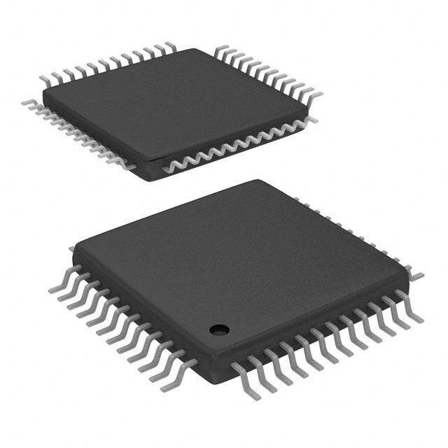
| 供应商器件封装 | 48-TQFP(7x7) |
| 其它名称 | ATM90E32AS-AU-RCT |
| 包装 | Digi-Reel® |
| 安装类型 | 表面贴装 |
| 封装/外壳 | 48-TQFP |
| 工作温度 | -40°C ~ 85°C |
| 应用说明 | |
| 标准包装 | 1 |
| 测量误差 | 0.5% |
| 电压-I/O低 | 0.4V, 0.8V |
| 电压-I/O高 | 3.2V, 5.5V |
| 电压-电源 | 2.8 V ~ 3.6 V |
| 电流-电源 | 13mA |
| 表计类型 | 3 相 |
| 输入阻抗 | 50 千欧, 80 千欧, 120 千欧 |


- 商务部:美国ITC正式对集成电路等产品启动337调查
- 曝三星4nm工艺存在良率问题 高通将骁龙8 Gen1或转产台积电
- 太阳诱电将投资9.5亿元在常州建新厂生产MLCC 预计2023年完工
- 英特尔发布欧洲新工厂建设计划 深化IDM 2.0 战略
- 台积电先进制程称霸业界 有大客户加持明年业绩稳了
- 达到5530亿美元!SIA预计今年全球半导体销售额将创下新高
- 英特尔拟将自动驾驶子公司Mobileye上市 估值或超500亿美元
- 三星加码芯片和SET,合并消费电子和移动部门,撤换高东真等 CEO
- 三星电子宣布重大人事变动 还合并消费电子和移动部门
- 海关总署:前11个月进口集成电路产品价值2.52万亿元 增长14.8%


PDF Datasheet 数据手册内容提取
Atmel M90E32AS Enhanced Poly-Phase High-Performance Wide-Span Energy Metering IC DATASHEET FEATURES Metering Features • Metering features fully in compliance with the requirements of IEC62052-11, IEC62053-22 and IEC62053-23, ANSI C12.1 and ANSI C12.20; applicable in poly- phase class 0.2S, 0.5S or class 1 watt-hour meter or class 2 var-hour meter. • Accuracy of ±0.1% for active energy and ±0.2% for reactive energy over a dynamic range of 6000:1. • Temperature coefficient is 6 ppm/ ℃ (typ.) for on-chip reference voltage. Automati- cally temperature compensated. • Single-point calibration on each phase over the whole dynamic range for active energy; no calibration needed for reactive/ apparent energy. • ±1℃ (typ.) temperature sensor accuracy. • Flexible piece-wise non-linearity compensation: three current (RMS value)-based segments with two programmable thresholds for each phase. Independent gain and phase angle compensation for each segment. • Electrical parameters measurement: less than ±0.5% fiducial error for Vrms, Irms, mean active/ reactive/ apparent power, frequency, power factor and phase angle. • Active (forward/reverse), reactive (forward/reverse), apparent energy with indepen- dent energy registers. • Programmable startup and no-load power thresholds. • 6 dedicated ADCs for phase A/B/C current and voltage sampling circuits. Current sampled over Current Transformer (CT) or Rogowski coil (di/dt coil); voltage sam- pled over resistor divider network. • Programmable power modes: Normal, Idle, Detection and Partial Measurement mode. • Fundamental (0.2%) and harmonic (1%) active energy with dedicated energy / power registers and independent energy outputs. • Current and voltage instantaneous signal monitoring. • Enhanced event detection: sag, over voltage, phase loss, over current, reverse V/I phase sequence, calculated neutral line current I over-current and frequency NC upper and lower threshold. Other Features • 3.3V single power supply. Operating voltage range: 2.8V~3.6V. Metering accuracy guaranteed within 3.0V~3.6V. • Four-wire SPI interface. • Programmable voltage sag detection and zero-crossing output. • Crystal oscillator frequency: 16.384MHz. On-chip two capacitors and no need of external capacitors. • Lower power consumption. I=13mA (typ.) in Normal mode. • TQFP48 package. • Operating temperature: -40℃ ~ +85℃. Atmel-46003B-SE-M90E32AS-Datasheet_02122015
APPLICATION • Poly-phase energy meters of class 0.2S, 0.5S and class 1 which are used in three-phase four-wire (3P4W, Y0) or three-phase three-wire (3P3W, Y or Δ) systems. • Power monitoring instruments which need to measure voltage, current, mean power, etc. GENERAL DESCRIPTION The M90E32AS is a poly-phase high performance wide-dynamic range metering IC. The M90E32AS incorporates 6 inde- pendent 2nd order sigma-delta ADCs, which could be employed in three voltage channels (phase A, B and C) and three current channels (phase A, B, C) in a typical three-phase four-wire system. The M90E32AS has an embedded DSP which executes calculation of active energy, reactive energy, apparent energy, fun- damental and harmonic active energy over ADC signal and on-chip reference voltage. The DSP also calculates measure- ment parameters such as voltage and current RMS value as well as mean active/reactive/apparent power. A four-wire SPI interface is provided between the M90E32AS and the external microcontroller. The M90E32AS is suitable for poly-phase multi-function meters which could measure active/reactive/apparent energy and fundamental/harmonic energy either through four independent energy pulse outputs CF1/CF2/CF3/CF4 or through the cor- responding registers. The ADC and auto-temperature compensation technology for reference voltage ensure the M90E32AS's long-term stability over variations in grid and ambient environment conditions. BLOCK DIAGRAM OSCI OSCO PM1 Power Mode PM0 Configuration VDD18 Regulator Crystal Oscillator Power On Reset CF1 RESET Energy Metering CF2 CF Out Current Detector (Forward/Reverse CF3 Active/Reactive/CF Generator) CF4 I1P / I1N ADC-I1 WarnOut I2P / I2N ADC-I2 DSP Flexible Piece-wise Non-linear Warn IRQ IRQ0 Compensation Out I3P / I3N ADC-I3 IRQ1 ZX0 Measure and Monitoring V1P / V1N ADC-V1 (V/I/rms / SAG / Phase / Zero ZX1 V2P / V2N ADC-V2 Frequency) Crossing ZX2 V3P / V3N ADC-V3 CS Temperature Sensor Control Logic SPI Interface SCLK SDO Vref On-chip SDI Reference Voltage Figure-1 M90E32AS Block Diagram 2 M90E32AS [Datasheet] Atmel-46003B-SE-M90E32AS-Datasheet_02122015
Table of Contents FEATURES.......................................................................................................................................... 1 APPLICATION..................................................................................................................................... 2 GENERAL DESCRIPTION................................................................................................................... 2 BLOCK DIAGRAM............................................................................................................................... 2 1 PIN ASSIGNMENT ..........................................................................................................................7 2 PIN DESCRIPTION ..........................................................................................................................8 3 FUNCTION DESCRIPTION ...........................................................................................................10 3.1 POWER SUPPLY ...................................................................................................................................................10 3.2 CLOCK ...................................................................................................................................................................10 3.3 RESET ....................................................................................................................................................................10 3.3.1 RESET Pin .................................................................................................................................................. 10 3.3.2 Power On Reset (POR) ............................................................................................................................. 10 3.3.3 Software Reset .......................................................................................................................................... 10 3.4 ANALOG/DIGITAL CHANNEL MAPPING ............................................................................................................11 3.5 METERING FUNCTION .........................................................................................................................................12 3.5.1 Theory of Energy Registers ..................................................................................................................... 12 3.5.2 Energy Registers ....................................................................................................................................... 13 3.5.3 Energy Pulse Output ................................................................................................................................. 14 3.5.4 Startup and No-load Power ...................................................................................................................... 14 3.6 MEASUREMENT FUNCTION ................................................................................................................................16 3.6.1 Active/ Reactive/ Apparent Power ........................................................................................................... 16 3.6.2 Fundamental / Harmonic Active Power ................................................................................................... 16 3.6.3 Mean Power Factor (PF) ........................................................................................................................... 16 3.6.4 Voltage / Current RMS .............................................................................................................................. 16 3.6.5 Phase Angle ............................................................................................................................................... 17 3.6.6 Frequency .................................................................................................................................................. 17 3.6.7 Temperature .............................................................................................................................................. 17 3.6.8 Peak Value ................................................................................................................................................. 17 3.7 POWER QUALITY MONITORING .........................................................................................................................18 3.7.1 Instantaneous Signal Monitoring ............................................................................................................ 18 3.7.2 Instantaneous Signal Related Status And Events ................................................................................. 19 3.7.3 Frequency Monitoring Related Status And Events ................................................................................ 20 3.7.4 Zero-Crossing Detection .......................................................................................................................... 20 3.7.5 Neutral Line Overcurrent Detection ........................................................................................................ 20 3.7.6 Phase Sequence Error Detection ............................................................................................................ 20 3.8 POWER MODE ......................................................................................................................................................21 3.8.1 Normal Mode (N Mode) ............................................................................................................................. 21 3.8.2 Idle Mode (I Mode) ..................................................................................................................................... 22 3.8.3 Detection Mode (D Mode) ......................................................................................................................... 24 3.8.4 Partial Measurement mode (M Mode) ...................................................................................................... 25 3.8.5 Transition of Power Modes ...................................................................................................................... 26 3.9 EXTERNAL COMPONENT COMPENSATION .....................................................................................................27 3.9.1 Gain Based Compensation ...................................................................................................................... 28 3.9.2 Delay/Phase Based Compensation ......................................................................................................... 29 M90E32AS [DATASHEET] 3 Atmel-46003B-SE-M90E32AS-Datasheet_02122015
4 SPI INTERFACE ............................................................................................................................30 4.1 INTERFACE DESCRIPTION .................................................................................................................................30 4.2 SPI INTERFACE ....................................................................................................................................................30 4.2.1 SPI Slave Interface Format ....................................................................................................................... 30 4.2.2 Reliability Enhancement Feature ............................................................................................................. 31 5 REGISTER .....................................................................................................................................32 5.1 REGISTER LIST ....................................................................................................................................................32 5.2 SPECIAL REGISTERS ..........................................................................................................................................39 5.2.1 Configuration Registers CRC Generation .............................................................................................. 39 5.2.2 IRQ and WarnOut Signal Generation ...................................................................................................... 40 5.2.3 Special Configuration Registers .............................................................................................................. 45 5.3 LOW-POWER MODES REGISTERS ....................................................................................................................48 5.3.1 Detection Mode Registers ........................................................................................................................ 48 5.3.2 Partial Measurement mode Registers ..................................................................................................... 50 5.4 CONFIGURATION AND CALIBRATION REGISTERS .........................................................................................55 5.4.1 Configuration Registers ........................................................................................................................... 55 5.4.2 Energy Calibration Registers ................................................................................................................... 57 5.4.3 Fundamental/Harmonic Energy Calibration registers ........................................................................... 58 5.4.4 Measurement Calibration ......................................................................................................................... 59 5.4.5 EMM Status ................................................................................................................................................ 59 5.5 ENERGY REGISTER .............................................................................................................................................67 5.5.1 Regular Energy Registers ........................................................................................................................ 67 5.5.2 Fundamental / Harmonic Energy Register .............................................................................................. 68 5.6 MEASUREMENT REGISTERS ..............................................................................................................................69 5.6.1 Power and Power Factor Registers ......................................................................................................... 69 5.6.2 Fundamental/ Harmonic Power and Voltage/ Current RMS Registers ................................................. 70 5.6.3 Peak, Frequency, Angle and Temperature Registers ............................................................................ 71 6 ELECTRICAL SPECIFICATION ....................................................................................................72 6.1 ELECTRICAL SPECIFICATION ............................................................................................................................72 6.2 METERING/ MEASUREMENT ACCURACY .........................................................................................................74 6.2.1 Metering Accuracy .................................................................................................................................... 74 6.2.2 Measurement Accuracy ............................................................................................................................ 75 6.3 INTERFACE TIMING .............................................................................................................................................76 6.3.1 SPI Interface Timing (Slave Mode) .......................................................................................................... 76 6.4 POWER ON RESET TIMING .................................................................................................................................77 6.5 ZERO-CROSSING TIMING ....................................................................................................................................78 6.6 VOLTAGE SAG AND PHASE LOSS TIMING .......................................................................................................79 6.7 ABSOLUTE MAXIMUM RATING ..........................................................................................................................80 ORDERING INFORMATION.............................................................................................................. 81 PACKAGE DIMENSIONS.................................................................................................................. 82 REVISION HISTORY ......................................................................................................................... 83 4 M90E32AS [Datasheet] Atmel-46003B-SE-M90E32AS-Datasheet_02122015
List of Tables Table-1 Pin Description .................................................................................................................................................... 8 Table-2 Power Mode Mapping ....................................................................................................................................... 21 Table-3 Digital I/O and Power Pin States in Idle Mode .................................................................................................. 22 Table-4 Compensation Related Registers ..................................................................................................................... 27 Table-5 Register List ...................................................................................................................................................... 32 Table-6 Configuration Registers .................................................................................................................................... 55 Table-7 Calibration Registers ........................................................................................................................................ 57 Table-8 Fundamental/Harmonic Energy Calibration Registers ...................................................................................... 58 Table-9 Measurement Calibration Registers ................................................................................................................. 59 Table-10 EMM Status Registers ...................................................................................................................................... 59 Table-11 Regular Energy Registers ................................................................................................................................. 67 Table-12 Fundamental / Harmonic Energy Register ........................................................................................................ 68 Table-13 Power and Power Factor Register .................................................................................................................... 69 Table-14 Fundamental/ Harmonic Power and Voltage/ Current RMS Registers ............................................................. 70 Table-15 Peak, Frequency, Angle and Temperature Registers ....................................................................................... 71 Table-16 Metering Accuracy for Different Energy within the Dynamic Range ................................................................. 74 Table-17 Measurement Parameter Range and Format ................................................................................................... 75 Table-18 SPI Timing Specification ................................................................................................................................... 76 Table-19 Power On Reset Specification .......................................................................................................................... 77 Table-20 Zero-Crossing Specification .............................................................................................................................. 78 M90E32AS [DATASHEET] 5 Atmel-46003B-SE-M90E32AS-Datasheet_02122015
List of Figures Figure-1 M90E32AS Block Diagram ................................................................................................................................. 2 Figure-2 Pin Assignment (Top View) ................................................................................................................................ 7 Figure-3 Channel to Phase Mapping .............................................................................................................................. 11 Figure-4 Energy Accumulation Diagram ......................................................................................................................... 13 Figure-5 CFx Pulse Output Regulation ........................................................................................................................... 14 Figure-6 Active Power Startup/Noload Processing ......................................................................................................... 14 Figure-7 Fundamental Active Power Startup/Noload Processing ................................................................................... 15 Figure-8 Harmonic Active Power Startup/Noload Processing ......................................................................................... 15 Figure-9 Power Quality Monitor in Datapath ................................................................................................................... 18 Figure-10 Block Diagram in Normal Mode ........................................................................................................................ 21 Figure-11 Block Diagram in Idle Mode .............................................................................................................................. 22 Figure-12 Block Diagram in Detection Mode .................................................................................................................... 24 Figure-13 Block Diagram in Partial Measurement mode .................................................................................................. 25 Figure-14 Power Mode Transition ..................................................................................................................................... 26 Figure-15 Segment Gain Compensation ........................................................................................................................... 28 Figure-16 Slave Mode ....................................................................................................................................................... 30 Figure-17 Read Sequence ................................................................................................................................................ 31 Figure-18 Write Sequence ................................................................................................................................................ 31 Figure-19 CRC Checking Diagram ................................................................................................................................... 39 Figure-20 IRQ and WarnOut Generation .......................................................................................................................... 40 Figure-21 Current Detection Register Latching Scheme .................................................................................................. 48 Figure-22 SPI Timing Diagram .......................................................................................................................................... 76 Figure-23 Power On Reset Timing (M90E32AS and MCU are Powered on Simultaneously) .......................................... 77 Figure-24 Power On Reset Timing in Normal & Partial Measurement Mode .................................................................... 77 Figure-25 Zero-Crossing Timing Diagram (per phase) ..................................................................................................... 78 Figure-26 Voltage Sag and Phase Loss Timing Diagram ................................................................................................. 79 M90E32AS [DATASHEET] 6 Atmel-46003B-SE-M90E32AS-Datasheet_02122015
1 PIN ASSIGNMENT D D D 18 18 ET K VD GN C C GN DD DD ES DI DO CL S D D N N D V V R S S S C 8 7 6 5 4 3 2 1 0 9 8 7 AVDD 1 4 4 4 4 4 4 4 4 4 3 3 336 IC AGND 2 35 NC I1P 3 34 PM1 I1N 4 33 PM0 I2P 5 32 TEST I2N 6 31 IRQ1 I3P 7 30 IRQ0 I3N 8 29 WarnOut IC 9 28 CF4 IC 10 27 CF3 Vref 11 26 CF2 AGND 12 25 CF1 3 4 5 6 7 8 9 0 1 2 3 4 1 1 1 1 1 1 1 2 2 2 2 2 V1P V1N V2P V2N V3P V3N GND OSCI SCO ZX0 ZX1 ZX2 D O Figure-2 Pin Assignment (Top View) M90E32AS [DATASHEET] 7 Atmel-46003B-SE-M90E32AS-Datasheet_02122015
2 PIN DESCRIPTION Table-1 Pin Description Name Pin No. I/O Type Description Reset: Reset Pin (active low) This pin should connect to ground through a 0.1 μF filter capacitor and a Reset 41 I LVTTL 10kΩ resistor to VDD. In application it can also directly connect to one out- put pin from microcontroller (MCU). AVDD: Analog Power Supply AVDD 1 I Power This pin provides power supply to the analog part. This pin should connect to DVDD and be decoupled with a 0.1μF capacitor. DVDD: Digital Power Supply DVDD 48 I Power This pin provides power supply to the digital part. It should be decoupled with a 10μF capacitor and a 0.1μF capacitor. VDD18: Digital Power Supply (1.8 V) VDD18 42, 43 P Power These two pins should be connected together and connected to ground through a 10μF capacitor. DGND 19, 44, 47 I Power DGND: Digital Ground AGND 2, 12 I Power AGND: Analog Ground I1P: Positive Input for Analog ADC Channel I1N: Negative Input for Analog ADC Channel I1P 3 I Analog These pins are differential inputs for analog ADC channel. I1N 4 These 6 analog ADC channels can be flexibly mapped, refer to 3.4 Analog/ 1 digital Channel Mapping. I2P: Positive Input for Analog ADC Channel I2N: Negative Input for Analog ADC Channel I2P 5 I Analog These pins are differential inputs for analog ADC channel. I2N 6 These 6 analog ADC channels can be flexibly mapped, refer to 3.4 Analog/ 1 digital Channel Mapping. I3P: Positive Input for Analog ADC Channel I3N: Negative Input for Analog ADC Channel I3P 7 I Analog These pins are differential inputs for analog ADC channel. I3N 8 These 6 analog ADC channels can be flexibly mapped, refer to 3.4 Analog/ 1 digital Channel Mapping. Vref: Output Pin for Reference Voltage Vref 11 O Analog This pin should be decoupled with a 4.7μF capacitor, it is better to add a 0.1μF ceramic capacitor. V1P: Positive Input for Analog ADC Channel V1N: Negative Input for Analog ADC Channel V1P 13 I Analog These pins are differential inputs for analog ADC channel. V1N 14 These 6 analog ADC channels can be flexibly mapped, refer to 3.4 Analog/ 1 digital Channel Mapping. V2P: Positive Input for Analog ADC Channel V2N: Negative Input for Analog ADC Channel V2P 15 I Analog These pins are differential inputs for analog ADC channel. V2N 16 These 6 analog ADC channels can be flexibly mapped, refer to 3.4 Analog/ 1 digital Channel Mapping. V3P: Positive Input for Analog ADC Channel V3N: Negative Input for Analog ADC Channel V3P 17 I Analog These pins are differential inputs for analog ADC channel. V3N 18 These 6 analog ADC channels can be flexibly mapped, refer to 3.4 Analog/ 1 digital Channel Mapping. 8 M90E32AS [Datasheet] Atmel-46003B-SE-M90E32AS-Datasheet_02122015
Table-1 Pin Description (Continued) Name Pin No. I/O Type Description OSCI 20 I OSC OSCI: External Crystal Input OSCO: External Crystal Output OSCO 21 O OSC A 16.384 MHz crystal is connected between OSCI and OSCO. There are two on-chip capacitors, therefore no need of external capacitors. ZX0 22 ZX2/ZX1/ZX0:Zero-Crossing Output ZX1 23 O LVTTL These pins are asserted when voltage or current crosses zero. Zero-cross- ZX2 24 ing mode can be configured by the ZXConfig register (07H). CF1 25 O LVTTL CF1: (all-phase-sum total) Active Energy Pulse Output CF2: (all-phase-sum total) Reactive/ Apparent Energy Pulse Output CF2 26 O LVTTL The output of this pin is determined by the CF2varh bit (b7, MMode0). CF3 27 O LVTTL CF3: (all-phase-sum total) Active Fundamental Energy Pulse Output CF4 28 O LVTTL CF4: (all-phase-sum total) Active Harmonic Energy Pulse Output WarnOut: Fatal Error Warning This pin is asserted high when there is metering related parameter check- WarnOut 29 O LVTTL sum error. Otherwise this pin stays low. Refer to 5.2.2 IRQ and WarnOut Signal Generation. IRQ0: Interrupt Output 0 This pin is asserted when one or more events in the EMMIntState0 register (1CCH) occur. It is deasserted when there is no bit set in the EMMIntState0 IRQ0 30 O LVTTL register (1CCH). In Detection mode, the IRQ0 is used to indicate the output of current detec- tor. The IRQ0 state is cleared when entering or exiting Detection mode. IRQ1: Interrupt Output 1 This pin is asserted when one or more events in the EMMIntState1 register (1D0H) occur. It is deasserted when there is no bit set in the EMMIntState1 IRQ1 31 O LVTTL register (1D0H). In Detection mode, the IRQ1 is used to indicate the output of current detec- tor. The IRQ1 state is cleared when entering or exiting Detection mode. PM0 33 PM1/0: Power Mode Configuration I2 LVTTL PM1 34 These two pins define the power mode of M90E32AS. Refer to Table-2. CS: Chip Select (Active Low) CS 37 I2 LVTTL In SPI mode, this pin must be driven from high to low for each read/ write operation, and maintain low for the entire operation. SCLK: Serial Clock SCLK 38 I2 LVTTL This pin is used as the clock for the SPI interface. Refer to 4 SPI Interface. SDO: Serial Data Output SDO 39 O LVTTL This pin is used as the data output for the SPI mode. Refer to 4 SPI Inter- face. SDI: Serial Data Input SDI 40 I2 LVTTL This pin is used as the data input for the SPI mode. Refer to 4 SPI Interface. TEST 32 I LVTTL This pin should be always connected to DGND in system application. IC 9, 10, 36 LVTTL These pins should be always connected to DGND in system application. NC 35, 45, 46 NC: These pins should be left open. Note 1: The channel mapping is only valid in Normal mode and Patial Measurement mode. Note 2: All the digital input pins except OSCI are 5 V compatible. M90E32AS [DATASHEET] 9 Atmel-46003B-SE-M90E32AS-Datasheet_02122015
3 FUNCTION DESCRIPTION 3.1 POWER SUPPLY The M90E32AS works with single power rail 3.3V. An on-chip voltage regulator regulates the 1.8V voltage for the digital logic. The regulated 1.8V power is connected to the VDD18 pin. It needs to be bypassed by an external capacitor. The M90E32AS has four power modes: Normal (N mode), Partial Measurement (M mode), Detection (D mode) and Idle (I mode). In Idle and Detection modes the 1.8V power regulator is not turned on and the digital logic is not powered. When the logic is not powered, all the configured register values are not kept (all context lost) except for Detection mode related registers (10H~13H) for Detection mode configuration. The registers in Partial Measurement mode or Normal mode have to be re-configured when transiting from Idle or Detec- tion mode. Refer to 3.8 Power Mode for power mode details. 3.2 CLOCK The M90E32AS has an on-chip oscillator and can directly connect to an external crystal. The OSCI pin can also be driven with a clock source. The oscillator will be powered down in Idle and Detection power modes, as described in 3.8 Power Mode. 3.3 RESET There are three reset sources for the M90E32AS: - RESET pin - On-chip Power On Reset circuit - Software Reset generated by the SoftReset register 3.3.1 RESET PIN The RESET pin can be asserted to reset the M90E32AS. The RESET pin has RC filter with typical time constant of 2μs in the I/O, as well as a 2μs (typical) de-glitch filter. Any reset pulse that is shorter than 2μs can not reset the M90E32AS. 3.3.2 POWER ON RESET (POR) The POR circuit resets the M90E32AS at power up. POR circuit triggers reset when: - DVDD power up with crossing the power-up threshold. Refer to Figure-24. - VDD18 regulator changing from disable to enable, i.e. from Idle or Detection mode to Partial Measurement mode or Normal mode. Refer to Figure-23. 3.3.3 SOFTWARE RESET Chip reset can be triggered by writing to the SoftReset register in Normal mode. The software reset is the same as the reset scope generated from the RESET pin or POR. These three reset sources have the same reset scope. All digital logics and registers except for some special registers will be subjected to reset. • Interface logic: clock dividers • Digital core/ logic: All registers except for some special registers. Refer to 5.3.1 Detection Mode Registers. 10 M90E32AS [Datasheet] Atmel-46003B-SE-M90E32AS-Datasheet_02122015
3.4 ANALOG/DIGITAL CHANNEL MAPPING Analog channel to digital channel mapping: The 6 analog ADC channels can be flexibly mapped to the 6 digital metering/measuring channels (V/I phase A/B/C). Refer to the ChannelMapI and ChannelMapU registers for configuration. Note that channel mapping is only valid in Normal mode and Patial Measurement mode. V CH_A Analog Digital V CH0 V CH_B V CH1 V CH2 I CH0 I CH1 V CH_C I CH2 I CH_A I CH_B I CH_C Flexible Channel mapping Figure-3 Channel to Phase Mapping M90E32AS [DATASHEET] 11 Atmel-46003B-SE-M90E32AS-Datasheet_02122015
3.5 METERING FUNCTION Metering is enabled when any of the MeterEn bits are set. When metering is not enabled, the CF pulse will not be generated and energy accumulator will not accumulate energy. All energy accumulation related status will be cleared, while startup/noload handling block related status will be still working. The accumulated energy will be converted to pulse frequency on the CF pins and stored in the corresponding energy reg- isters. 3.5.1 THEORY OF ENERGY REGISTERS The energy accumulation runs at 1 MHz clock rate by accumulating the power value calculated by the DSP processor. The power accumulation process is equivalent to digitally integrating the instantaneous power with a delta-time of about 1us. The accumulated energy is used to calculate the CF pulses and the corresponding internal energy registers. The accumulated energy is converted to frequency of the CF pulses. One CF usually corresponds to 1KWh / MC (MC is Meter Constant, e.g. 3200 imp/kWh), and is usually referenced as an energy unit in this datasheet. The internal energy res- olution for accumulation and conversion is 0.01 CF. The 0.01 CF pulse energy constant is referenced as 'PL_constant'. Within 0.01 CF, forward and reverse energy are counteracted. When energy exceeds 0.01 pulse, the respective forward/ reverse energy is increased. Take the example of active energy. Suppose: T0: Forward energy register is 12.34 pulses and reverse energy register is 1.23 pulses. From t0 to t1: 0.005 forward pulses appeared. From t1 to t2: 0.004 reverse pulses appeared. From t2 to t3: 0.005 reverse pulses appeared. From t3 to t4: 0.007 reverse pulses appeared. The following table illustrates the process of energy accumulation process: t0 t1 t2 t3 t4 Input energy + 0.005 -0.004 -0.005 -0.007 Bidirectional energy accumulator 0.005 0.001 -0.004 -0.001 Forward 0.01 CF 0 0 0 0 Reverse 0.01CF 0 0 0 1 Forward energy register 12.34 12.34 12.34 12.34 12.34 Reverse energy register 1.23 1.23 1.23 1.23 1.24 When forward/reverse energy reaches 0.01 pulse, the respective register is updated. When forward or reverse energy reaches 1 pulse, CFx pins output pulse and the CFxRevST bits (b3~0, EMMState0) are updated. Refer to Figure-4. 12 M90E32AS [Datasheet] Atmel-46003B-SE-M90E32AS-Datasheet_02122015
A/B/C Bi-directional Energy Phase-A accuBmi-duilraetcotri,o nal (+)0.01 Forward pPhears-e Phase-B prooalslc iocrtEBoiuvvnliemel- edrEo/u rivngrlaeeeytcr ro tgiroy, n al CF(+)C0F.01 acceunmeFreuognlaryew troagrryd Power Phase-C ne0g.an0te1pi0vagCon.eca0sFe pcrt1i0@iogtuoviC.val0mesl eFt1i oitu@/viCvvleaeeF tr@/o r , (-)C0F.(0-)1C0 ((F.+-0))CC100 FF..001a1 Bc ceauaacnmBcckeccwreauAguucnalBcaymmkeFrcEE tadwroouuucgnn rarllmkaayeewrw ttrrduaoogga lrrrayydr td o r [P/Q]Ereg[A/B/C]PST Accumulator total Pos-CF Accumulator Bi-directional [P/Q]EregTPST Energy All-phase accroulml ouvlaetro r, (+)C0F.01 FEonrewragryd A/B/C sum Power positive/ Accumulator negative @ 0.01CF (-)0.01 Backward CF Energy CF Gen CF pulse Accumulator Logic Neg-CF Accumulator CF[1/2/34]RevST Figure-4 Energy Accumulation Diagram For all-phase-sum total of active, reactive and (arithmetic sum) apparent energy, the associated power is obtained by sum- ming the power of the three phases. The accumulation method of all-phase-sum energy is determined by the EnPC/EnPB/ EnPA/ABSEnP/ABSEnQ bits (b0~b4, MMode0). Note that the direction of all-phase-sum power and single-phase power might be different. 3.5.2 ENERGY REGISTERS The M90E32AS meters non-decomposed total active, reactive and apparent energy, as well as decomposed active funda- mental and harmonic energy. The registers are listed as below. 3.5.2.1 Total Energy Registers Each phase and all-phase-sum has the following registers: - Active forward/ reverse - Reactive forward/ reverse - Apparent energy Altogether there are 20 energy registers. Those registers are defined in 5.5.1 Regular Energy Registers. 3.5.2.2 Fundamental and Harmonic Energy Registers The M90E32AS counts decomposed active fundamental and harmonic energy. Reactive energy is not decomposed to fun- damental and harmonic. The fundamental/harmonic energy is accumulated in the same way as active energy accumulation method described above. Registers: - Fundamental / harmonic - all-phase-sum / phase A / phase B / phase C - Forward / reverse Altogether there are 16 energy registers. Refer to 5.5.2 Fundamental / Harmonic Energy Register. M90E32AS [DATASHEET] 13 Atmel-46003B-SE-M90E32AS-Datasheet_02122015
3.5.3 ENERGY PULSE OUTPUT CF1 is fixed to be total active energy output (all-phase-sum). Both forward and reverse energy registers can generate the CF pulse (change of forward/ reverse direction can generate an interrupt if enabled). CF2 is reactive energy output (all-phase-sum) by default. It can also be configured to be arithmetic sum apparent energy output (all-phase-sum). CF3 is fixed to be active fundamental energy output (all-phase-sum). CF4 is fixed to be active harmonic energy output (all-phase-sum). T =80ms p T =0.5T p CFx T≥160ms 10ms≤T<160ms Figure-5 CFx Pulse Output Regulation For CFx pulse width regulation, refer to Figure-5. Case1 T>=160ms, Tp=80ms Case 2 10ms<=T<160ms, Tp=T/2 3.5.4 STARTUP AND NO-LOAD POWER There are startup power threshold registers (e.g. PStartTh(35H)). Refer to 5.4 Configuration and Calibration Registers. The power threshold registers are defined for all-phase-sum active, reactive and apparent power. The M90E32AS starts meter- ing when the corresponding all-phase-sum power is greater than the startup threshold. When the power value is lower than the startup threshold, energy is not accumulated and it is assumed as in no-load status. Refer to Figure-6. There are also no-load Current Threshold registers for Active, Reactive and Apparent energy metering participation for each of the 3 phases. If |P|+|Q| is lower than the corresponding power threshold, that particular phase will not be accumu- lated. Refer to the PStartTh register and other threshold registers. There are also no-load status bits (the TPnoload/TQnoload bits (b14~15, Fundamental / Harmonic Energy Register)) defined to reflect the no-load status. The M90E32AS does not output any pulse in no-load status. The power-on state is of no-load status. Phase |P| + |Q| > C PPhaseTh? NC E c B Phase |P| + |Q| > ati PoPwhears efr oAmct iDveS P PhaPsPe h|Pa1s| e+T |hQ?| > NB Arithm + Total Active Power 0 01 EnTeorgtayl MAcettievrein g PoPAwhears efr oAmct iDveS P 0PPha1s0eTh? E BS or PSAtBaSrtT >h ? A A Phase Active 0 10 EN NoLoad Status Power from DSP 1 Phase Active 0 0 Energy Metering 0 0 Active Power Startup/Noload handling Figure-6 Active Power Startup/Noload Processing 14 M90E32AS [Datasheet] Atmel-46003B-SE-M90E32AS-Datasheet_02122015
C Phase |P| + |Q| > C Total Active Power PPhaseTh? N E c PBoPwhears efr oAmct iDveS P PPhhaPassPee h| Pa|P1s| |e+ +T | hQ|Q?| |> > NB Arithmati + Total PAoctwiveer Fund 0 01 TEontaelr gAyc Mtiveet eFruinngd PAoPwhears efr oAmct iDveS P 0PPha1s0eTh? E BS or PSAtBaSrtT >h ? PFuhnadsaem Aecntitvael 0 10 ENA A NoLoad Status Power from DSP 1 Phase Active 0 0 Fund Energy 0 0 Metering Active Power startup/Noload handling Figure-7 Fundamental Active Power Startup/Noload Processing C PhPasPeh a|Ps|e +T h|Q?| > NC Total Active Power E c Total Active Harmonic B Phase |P| + |Q| > ati Power Total Active APoPwhears efr oAmct iDveS P PhaPsPe h|Pa1s| e+T |hQ?| > NB Arithm + 0 01 HarmMoentiecr iEnngergy PPoPhwhaeasres e f(r AoAmcctt iivDveeS P 0PPha1s0eTh? E BS or PSAtBaSrtT >h ? Total Power - A A Active 0 10 EN NoLoad Status Fundamental 1 Power) from DSP 0 0 Phase Active Harmonic Energy 0 0 Metering Active Power startup/Noload handling Figure-8 Harmonic Active Power Startup/Noload Processing M90E32AS [DATASHEET] 15 Atmel-46003B-SE-M90E32AS-Datasheet_02122015
3.6 MEASUREMENT FUNCTION Measured parameters can be divided to 8 types as follows: - Active/ Reactive/ Apparent Power - Fundamental/ Harmonic Power - RMS for Voltage and Current - Power Factor - Phase Angle - Frequency - Temperature - Peak Value Measured parameters are average values that are averaged among 16 phase-voltage cycles (about 320ms at 50Hz) except for the temperature. The measured parameter update frequency is approximately 3Hz. Refer to Table-17. 3.6.1 ACTIVE/ REACTIVE/ APPARENT POWER Active/ Reactive/ Apparent Power measurement registers can be divided as below: - active, reactive, apparent power - all-phase-sum / phase A / phase B / phase C Altogether there are 12 power registers. Refer to 5.6.1 Power and Power Factor Registers. Per-phase apparent power is defined as the product of measured Vrms and Irms of that phase. All-phase-sum power is measured by arithmetically summing the per-phase measured power. The summing of phases can be configured by the MMode0 register. 3.6.2 FUNDAMENTAL / HARMONIC ACTIVE POWER Fundamental / harmonic active power measurement registers can be divided as below: - fundamental and harmonic power - all-phase-sum / phase A / phase B / phase C Altogether there are 8 power registers. Refer to 5.6.2 Fundamental/ Harmonic Power and Voltage/ Current RMS Registers. 3.6.3 MEAN POWER FACTOR (PF) Power Factor is defined for those cases: all-phase-sum / phase A / phase B / phase C. Altogether there are 4 power factor registers. Refer to 5.6.1 Power and Power Factor Registers. For all-phase: All_phase_sum active_power PF_all = All_phase_sum apparent_power For each of the phase:: active_power PF_phase = apparent_power 3.6.4 VOLTAGE / CURRENT RMS Voltage/current RMS registers can be divided as follows: Per-phase: Phase A / Phase B / Phase C Voltage / Current Neutral Line Current RMS: Neutral line current can be calculated by instantaneous value i =i +i +i . N A B C Altogether there are 7 RMS registers. Refer to 5.6.2 Fundamental/ Harmonic Power and Voltage/ Current RMS Registers. 16 M90E32AS [Datasheet] Atmel-46003B-SE-M90E32AS-Datasheet_02122015
3.6.5 PHASE ANGLE Phase Angle measurement registers can be divided as below: - phase A / phase B / phase C - voltage / current Altogether there are 6 phase angle registers. Refer to 5.6.3 Peak, Frequency, Angle and Temperature Registers. Phase Angle is measured by the time-difference between the Voltage and Current channel of the same phase. 3.6.6 FREQUENCY The frequency is measured basing on the zero-crossing point of voltage channels. The phase A voltage signal zero-crossing will be used to compute the frequency. If phase A is in the SAG condition, phase C will be used. If phase C is also in SAG condition, phase B will be used. If all the phases are in the SAG condition, Frequency will be measured based on the channels which are not in phaseLoss condition (with the same order). If all phases are lost, the frequency will return zero. The frequency data is not averaged (updated cycle by cycle). Refer to 5.6.3 Peak, Frequency, Angle and Temperature Registers. 3.6.7 TEMPERATURE Chip Junction-Temperature is measured roughly every 100 ms by on-chip temperature sensor. Refer to 5.6.3 Peak, Frequency, Angle and Temperature Registers. 3.6.8 PEAK VALUE Altogether there are 6 peak value registers. Refer to 5.6.3 Peak, Frequency, Angle and Temperature Registers. Refer to 3.7.1 Instantaneous Signal Monitoring. M90E32AS [DATASHEET] 17 Atmel-46003B-SE-M90E32AS-Datasheet_02122015
3.7 POWER QUALITY MONITORING Phase -C Phase -B Phase -A offset V-channel PGA ADC map + ZX OV Detector Peak Sag PhaseLoss Detector Detector Detector Phase Sequence, Frequency Frequency Range offset I-channel PGA ADC map + ZX DSP Freq based 50/60 Phase Comp Angle Peak OI Detector Detector Figure-9 Power Quality Monitor in Datapath 3.7.1 INSTANTANEOUS SIGNAL MONITORING Peak detection function: Peak value for each channel was detected within timing period configured by the PeakDet_period bits (b15~8, SagPeak- DetCfg). The detected peak value is updated on period intersection. Registers: The peak value detected can be accessed through register U/I Peak registers. Refer to 5.6.3 Peak, Frequency, Angle and Temperature Registers. 18 M90E32AS [Datasheet] Atmel-46003B-SE-M90E32AS-Datasheet_02122015
3.7.2 INSTANTANEOUS SIGNAL RELATED STATUS AND EVENTS The registers involved are OVth, OIth, SagTh, PhaseLossTh and SagPeakDetCfg. The result can be reflected in EMMState0 and EMMState1 registers, as well as EMMIntState0 and EMMIntState1 registers if the corresponding bits in EMMIntEn0/EMMIntEn1 registers are set. The threshold value has the following relationship with the RMS register (MSB-16bit): RmsRegValue∗ 2 xxThRegValue = VIgain 14 2 Here VIgain is Ugain register value or Igain register value. 3.7.2.1 Sag Detection Usually in the application the Sag threshold is set to be 78% of the reference voltage. The M90E32AS generates Sag event when there are less than three 8KHz samples (absolute value) greater than the sag threshold in one detecting period. Refer to 6.6 Voltage Sag and Phase Loss Timing. The detecting period length can be configured by the Sag_Period bits (b7~0, SagPeakDetCfg). Sag status is asserted when there is no voltage instantaneous sample's absolute value goes beyond the Sag threshold in any phase. Sag status is cleared when there are three samples detected with absolute value above the Sag threshold. For the computation of Sag threshold register value, refer to application note 46103. The Sag event is captured by the SagPhaseIntST bits (b14-12, EMMIntState1). If the corresponding IRQ enable bits the SagPhaseIntEN bits (b14-12, EMMIntEn1) is set, IRQ can be generated. Refer to Figure-26. 3.7.2.2 Phase Loss Detection The phase loss detection detects if there is one or more phases’ voltage is less than the phase-loss threshold voltage. The processing and handling is similar to sag detection, only the threshold is different. The threshold computation flow is also similar. The typical threshold setting could be 10% Un or less. If any phase line is detected as in phase-loss mode, that phase’s zero-crossing detection function (both voltage and cur- rent) is disabled. 3.7.2.3 Over Voltage (OV) Detection When any phase's absolute voltage sample instantaneous value goes beyond the over voltage threshold, the Over Voltage status is asserted. The status is de-asserted when the voltage sample instantaneous value go back below the over voltage threshold. Change of the Over Voltage status can generate interrupt and flagged in the EMMState0 and EMMIntState0 registers. 3.7.2.4 Over Current (OI) Detection When any phase's absolute current sample instantaneous value go beyond the over current threshold, the Over Current status is asserted. The status is de-asserted when the current sample instantaneous value go back below the over current threshold. Change of the Over Current status can generate interrupt and flagged in the EMMState0 and EMMIntState0 registers. M90E32AS [DATASHEET] 19 Atmel-46003B-SE-M90E32AS-Datasheet_02122015
3.7.3 FREQUENCY MONITORING RELATED STATUS AND EVENTS The measured frequency is compared with two thresholds configured in the the FreqLoTh register and the FreqHiTh regis- ter. If the measured frequency goes beyond the range defined by the two thresholds, the FreqLoST bit (b11, EMMState1) and FreqHiST bit (b15, EMMState1) will be asserted. The interrupt status will be updated as well; and if enabled, interrupt signal can be asserted. 3.7.4 ZERO-CROSSING DETECTION Zero-crossing detector detects the zero-crossing point of the fundamental component of voltage and current for each of the 3 phases. Refer to 6.5 Zero-Crossing Timing. Zero-crossing signal can be independently configured and output. Refer to the definition of the ZXConfig register. 3.7.5 NEUTRAL LINE OVERCURRENT DETECTION The neutral line rms current (calculated) I is checked with the threshold defined in the InWarnTh register. If the N Line NC current is greater than the threshold, the INOv0ST bit (b7, EMMState0) is set. IRQ0 is generated if the INOv0IntEN bit (b7, EMMIntEn0) is set. 3.7.6 PHASE SEQUENCE ERROR DETECTION The phase sequence is detected in two cases: 3P4W and 3P3W, which is defined by the 3P3W bit (b8, MMode0). 3P4W case: Correct sequence: Voltage/current zero-crossing sequence: phase-A, phase-B and phase-C. 3P3W case: Correct sequence: Voltage/current zero-crossing between phase-A and phase-C is greater than 180 degree. If the above mentioned criteria are violated, it is assumed as a phase sequence error, the URevWnST bit (b9, EMMState0) or the IRevWnST bit (b9, EMMState0) will be set. 20 M90E32AS [Datasheet] Atmel-46003B-SE-M90E32AS-Datasheet_02122015
3.8 POWER MODE The M90E32AS has four power modes. The power mode is solely defined by the PM1 and PM0 pins. Table-2 Power Mode Mapping PM1:PM0 Value Power Mode 11 Normal (N mode) 10 Partial Measurement (M mode) 01 Detection (D mode) 00 Idle (I mode) 3.8.1 NORMAL MODE (N MODE) In Normal mode, the default is that all function blocks are active except for current detector block. Refer to Figure-10. The current detector can be enabled and calibrated in normal mode using control bits in DetectCtrl register. OSCI OSCO PM1 Power Mode PM0 Configuration VDD18 Regulator Crystal Oscillator Power On Reset CF1 RESET Energy Metering CF2 CF Out Current Detector (Forward/Reverse CF3 Active/Reactive/CF Generator) CF4 I1P / I1N ADC-I1 WarnOut I2P / I2N ADC-I2 DSP Flexible Piece-wise Non-linear Warn IRQ IRQ0 Compensation Out I3P / I3N ADC-I3 IRQ1 ZX0 Measure and Monitoring V1P / V1N ADC-V1 (V/I/rms / SAG / Phase / Zero ZX1 V2P / V2N ADC-V2 Frequency) Crossing ZX2 V3P / V3N ADC-V3 CS Temperature Sensor Control Logic SPI Interface SCLK SDO Vref On-chip SDI Reference Voltage Disabled Figure-10 Block Diagram in Normal Mode M90E32AS [DATASHEET] 21 Atmel-46003B-SE-M90E32AS-Datasheet_02122015
3.8.2 IDLE MODE (I MODE) In Idle mode, all functions are shut off. The analog blocks' power supply is powered but circuits are set into power-down mode, i.e, power supply applied but all current paths are shut off. There is very low current since only very low device leakage could exist in this mode. The digital I/Os' supply is powered. In I/O and analog interface, the input signals from digital core (which is not powered) will be set to known state as described in Table-3. The PM1 and PM0 pins which are controlled by external MCU are active and can configure the M90E32AS to other modes. OSCI OSCO PM1 Power Mode PM0 Configuration VDD18 Regulator Crystal Oscillator Power On Reset CF1 RESET Energy Metering CF2 CF Out Current Detector (Forward/Reverse CF3 Active/Reactive/CF Generator) CF4 I1P / I1N ADC-I1 WarnOut I2P / I2N ADC-I2 DSP Flexible Piece-wise Non-linear Warn IRQ IRQ0 Compensation Out I3P / I3N ADC-I3 IRQ1 ZX0 Measure and Monitoring V1P / V1N ADC-V1 (V/I/rms / SAG / Phase / Zero ZX1 V2P / V2N ADC-V2 Frequency) Crossing ZX2 V3P / V3N ADC-V3 CS Temperature Sensor Control Logic SPI Interface SCLK SDO Vref On-chip SDI Reference Voltage Disabled Figure-11 Block Diagram in Idle Mode Please note that since the digital I/O is not shut off, the I/O circuit is active in the Idle mode. The application shall make sure that valid logic levels are applied to the I/O. Table-3 lists digital I/O and power pins’ states in Idle mode. It lists the requirements for inputs and the output level for out- put. Table-3 Digital I/O and Power Pin States in Idle Mode Name I/O type Type Pin State in Idle Mode Reset I LVTTL Input level shall be VDD33. I/O set in input mode. CS I LVTTL Input level shall be VDD33 or VSS. I/O set in input mode. SCLK I LVTTL Input level shall be VDD33 or VSS. I/O set in input mode. SDO O LVTTL Input level shall be VDD33 or VSS. I/O set in input mode. SDI I LVTTL Input level shall be VDD33 or VSS. PM1 I LVTTL PM0 As defined in Table-2. 22 M90E32AS [Datasheet] Atmel-46003B-SE-M90E32AS-Datasheet_02122015
Table-3 Digital I/O and Power Pin States in Idle Mode (Continued) Name I/O type Type Pin State in Idle Mode OSCI I Oscillator powered down. OSC OSCO O OSCO stays at fixed (low) level. ZX0 ZX1 O LVTTL 0 ZX2 CF1 CF2 O LVTTL 0 CF3 CF4 WarnOut O LVTTL 0 IRQ0 O LVTTL 0 IRQ1 VDD18 I Power Regulated 1.8V: high impedance DVDD I Power Digital Power Supply: powered by system AVDD I Power Analog Power Supply: powered by system Test I Input Always tie to ground in system application M90E32AS [DATASHEET] 23 Atmel-46003B-SE-M90E32AS-Datasheet_02122015
3.8.3 DETECTION MODE (D MODE) In Detection mode, the current detector is active. The current detector compares whether any phase current exceeds the configured threshold using low-power comparators. When the current of one phase or multiple phases exceeds the configured threshold, the M90E32AS asserts the IRQ0 pin to high and hold it until power mode change. The IRQ0 state is cleared when entering or exiting Detection mode. When the current of all three current channels exceed the configured threshold, the M90E32AS asserts the IRQ1 pin to high and hold it until power mode change. The IRQ1 state is cleared when entering or exiting Detection mode. The threshold registers need to be programmed in Normal mode before entering Detection mode. The digital I/O state is the same as that in Idle state (except for IRQ0/IRQ1 and PM1/PM0). The M90E32AS has two comparators for detecting each phase’s positive and negative current. Each comparator’s thresh- old can be set individually. The two comparators are both active by default, which called ‘double-side detection’. User also can enable one comparator only to save power consumption, which called ‘single-side detection’. Double-side detection has faster response and can detect ‘half-wave’ current. But it consumes nearly twice as much power as single-side detection. Comparators can be power-down by configuring the DetectCtrl register. The current detector can be enabled and calibrated in normal mode using control bits in the DetectCtrl register. OSCI OSCO PM1 Power Mode PM0 Configuration VDD18 Regulator Crystal Oscillator Power On Reset CF1 RESET Energy Metering CF2 CF Out Current Detector (Forward/Reverse CF3 Active/Reactive/CF Generator) CF4 I1P / I1N ADC-I1 WarnOut I2P / I2N ADC-I2 DSP Flexible Piece-wise Non-linear Warn IRQ IRQ0 Compensation Out I3P / I3N ADC-I3 IRQ1 ZX0 Measure and Monitoring V1P / V1N ADC-V1 (V/I/rms / SAG / Phase / Zero ZX1 V2P / V2N ADC-V2 Frequency) Crossing ZX2 V3P / V3N ADC-V3 CS Temperature Sensor Control Logic SPI Interface SCLK SDO Vref On-chip SDI Reference Voltage Disabled Figure-12 Block Diagram in Detection Mode 24 M90E32AS [Datasheet] Atmel-46003B-SE-M90E32AS-Datasheet_02122015
3.8.4 PARTIAL MEASUREMENT MODE (M MODE) In this mode, all the measurements are through the same hardware that does the measurement in the normal mode. To save power, the energy accumulation block and a portion of the DSP computation code will not be running in this mode. In this mode, There are configuration bits in the PMPwrCtrl register to get lower power if the application allows: • Option to turn-off the three analog voltage channel if there is no need to measure voltage and power. • Option to lower down the digital clock from 16.384Mhz to 8.192MHz In Partial Measurement mode, CRC checking will be disabled. The interrupts will not be generated. OSCI OSCO PM1 Power Mode PM0 Configuration VDD18 Regulator Crystal Oscillator Power On Reset CF1 RESET Energy Metering CF2 CF Out Current Detector (Forward/Reverse CF3 Active/Reactive/CF Generator) CF4 I1P / I1N ADC-I1 WarnOut I2P / I2N ADC-I2 DSP Flexible Piece-wise Non-linear Warn IRQ IRQ0 Compensation Out I3P / I3N ADC-I3 IRQ1 ZX0 Measure and Monitoring V1P / V1N ADC-V1 (V/I/rms / SAG / Phase / Zero ZX1 V2P / V2N ADC-V2 Frequency) Crossing ZX2 V3P / V3N ADC-V3 CS Temperature Sensor Control Logic SPI Interface SCLK SDO Vref On-chip SDI Reference Voltage Disabled Figure-13 Block Diagram in Partial Measurement mode M90E32AS [DATASHEET] 25 Atmel-46003B-SE-M90E32AS-Datasheet_02122015
3.8.5 TRANSITION OF POWER MODES The above power modes are controlled by the PM0 and PM1 pins. In application, the PM0 and PM1 pins are connected to external MCU. The PM0 and PM1 pins have internal RC- filters. Generally, the M90E32AS stays in Idle mode most of the time while outage. It enters Detection mode at a certain interval (for example 5s) as controlled by the MCU. It informs the MCU if the current exceeds the configured threshold. The MCU then commands the M90E32AS to enter Partial Measurement mode at a certain interval (e.g. 60s) to read related current. After current reading, the M90E32AS gets back to the Idle mode. The measured current may be used to count energy according to some metering model (like current RMS multiplying the rated voltage to compute the power). Any power mode transition goes through the Idle mode, as shown in Figure-14. Normal Mode Idle Mode Detection Mode Partial Measurement Mode Figure-14 Power Mode Transition 26 M90E32AS [Datasheet] Atmel-46003B-SE-M90E32AS-Datasheet_02122015
3.9 EXTERNAL COMPONENT COMPENSATION The calibrated channel gain and phase-delay offset could be tuned with respect to some reference parameter. This feature is useful when external component is not ideal and allow low cost sensors used in the system. There are three reference parameters: • Measured Current RMS (per phase) • Measured line frequency (all phase in common) • Measured temperature There are two tuning parameters to compensate: • Channel gain compensation • Channel phase delay compensation Following are the compensation correspondences: • Measured current RMS is per phase. It goes to Igain and Phi for each phase. • This is to compensate the non-linearity of current sensors, like a Current-Transformer. Non-linearity can be gain-non- linearity or phase nonlinearity. The gain nonlinearity is compensated by Igain compensation and phase nonlinearity is compensated by phase compensation. • Frequency compensation only goes to Phi/Delay (all phases are the same). • Temperature compensation only goes to UGain (per phase). Table-4 Compensation Related Registers Parameter Describtion Registers LogIrms Measured Current RMS LOGIrms0, LOGIrms1 F0 Nominal line frequency F0 T0 Nominal temperature T0 GainAIrms01, GainAIrms2, GainBIrms01, GainBIrms2, GainIrms Gain compensation for Irms GainCIrms01, GainCIrms2 PhiAIrms01, PhiAIrms2, PhiBIrms01, PhiBIrms2, PhiCIrms01, PhiIrms Phase compensation for Irms PhiCIrms2 UGainT Temperature compensation only goes to UGain UGainTAB, UGainTC PhiF Frequency compensation only goes to Phi/Delay PhiFreqComp M90E32AS [DATASHEET] 27 Atmel-46003B-SE-M90E32AS-Datasheet_02122015
3.9.1 GAIN BASED COMPENSATION The channel gain can be tuned automatically according to measured temperature and current RMS. Channel_Gain GainIrms*(Log(Irms )) Irms_ref = Gain0 * 1+ + GainIrms_offset 19 2 UGainT*(T-T0) Channel_Gain_Voltage = UGain0 * 1+ 20 2 Here Log(x) = Log (x)*16, e.g.: Log(2) = 16, Log(16) = 64 2 • Gain0 is the calibrated Gain at nominal condition, • GainIrms is the gain adjustment per Irms change (8 bit) • Irms_ref is the reference current RMS • GainIrms_offset is the offset for segment calibration • UGain0 is the calibrated Gain at nominal temperature • UGainT is the gain adjustment per temperature degree change, • T0 is the nominal temperature, If (Irms > Irms0) GainIrms = GainIrms0, Irms_ref = Irms0, GainIrms_offset = 0, If (Irms1<Irms < Irms0) GainIrms = GainIrms1, Irms_ref = Irms0, GainIrms_offset = 0, If (Irms < Irms1) GainIrms = GainIrms2, Irms_ref = Irms1 GainIrms1*(Log(Irms1 )) Irms0 GainIrms_offset = 219 Delta-Gain Delta-Phi Delta-Gain Irms1 Irms0 Log(Irms) Delta-Phi GainIrms2 GainIrms1 GainIrms0 PhiIrms2 PhiIrms1 PhiIrms0 Figure-15 Segment Gain Compensation 28 M90E32AS [Datasheet] Atmel-46003B-SE-M90E32AS-Datasheet_02122015
3.9.2 DELAY/PHASE BASED COMPENSATION The Channel phase compensation delay can be tuned according to the measured frequency and current RMS. Channel_Phi PhiIrms*(Log(Irms )) PhiF*(F-F0) Irms_ref =Phi0+ + + Phi_offset 512 256 • Phi0 is the calibrated delay between the V/I channel (in terms of 2.048Mhz clock cycles) • PhiF is the delay change per frequency change • F0 is the nominal frequency, • PhiIrms is the delay change per current change • Phi_offset is the offset for segment calibration • Log(x)= Log (x)*16 2 If (Irms > Irms0) PhiIrms = PhiIrms0, Irms_ref = Irms0, Phi_offset=0 If (Irms1<Irms < Irms0) PhiIrms= PhiIrms1, Irms_ref = Irms0, Phi_offset=0 If (Irms < Irms1) PhiIrms = PhiIrms2, Irms_ref = Irms1, PhiIrms1*(Log(Irms1 )) Irms0 Phi_offset = 256 Implementation Note: The channel_phi could be computed at the 8Khz rate. The computed channel_phi (before applied to the delay chain in the decimator) shall be averaged and updated every 8192 8Khz-samples (about one update per second). This is to attenuate the fluctuation generated in the computation when the current is small and avoid frequent updating of the delay, which is assumed to be a fixed value in the decimator. M90E32AS [DATASHEET] 29 Atmel-46003B-SE-M90E32AS-Datasheet_02122015
4 SPI INTERFACE 4.1 INTERFACE DESCRIPTION Four pins are associated with the interface as below: • SDI – Data pin, input. • SDO – Data pin, output. • SCLK – Clock input pin. • CS – Chip select pin Input. SPI Interface logic Host controller in (As slave) master mode MOSI SDI MOSI MISO SDO MISO SCK SCLK SCK CS CS GPIO1 Figure-16 Slave Mode 4.2 SPI INTERFACE The interface works in slave mode as shown in Figure-16. 4.2.1 SPI SLAVE INTERFACE FORMAT In the SPI mode, data on SDI is shifted into the chip on the rising edge of SCLK while data on SDO is shifted out of the chip on the falling edge of SCLK. Refer to Figure-17 and Figure-18 below for the timing diagram. Access type: The first bit on SDI defines the access type as below: Instruction Instruction Description Format Read read from registers 1 Write write to registers 0 Address: Fixed 15-bit, following the access type bits. The lower 10-bit is decoded as address; the higher 5 bits are ‘Don't Care’. Read/Write data: Fixed as 16 bits. Read Sequence: 30 M90E32AS [Datasheet] Atmel-46003B-SE-M90E32AS-Datasheet_02122015
CS 1 2 3 4 5 6 7 8 9 10 11 12 13 14 15 16 17 18 19 20 21 22 23 24 25 26 27 28 29 30 31 32 SCLK Register Address SDI X X X X X A9 A8 A7 A6 A5 A4 A3 A2 A1 A0 Don't care 16-bit data High Impedance SDO D15 D14 D13 D12 D11 D10 D9 D8 D7 D6 D5 D4 D3 D2 D1 D0 Figure-17 Read Sequence Write Sequence: CS 1 2 3 4 5 6 7 8 9 10 11 12 13 14 15 16 17 18 19 20 21 22 23 24 25 26 27 28 29 30 31 32 SCLK Register Address 16-bit data SDI X X X X X A9 A8 A7 A6 A5 A4 A3 A2 A1 A0 D15 D14 D13 D12 D11 D10 D9 D8 D7 D6 D5 D4 D3 D2 D1 D0 High Impedance SDO Figure-18 Write Sequence 4.2.2 RELIABILITY ENHANCEMENT FEATURE The SPI read/write transaction is CS-low defined. Each transaction can only access one register. Within each CS-low defined transaction: Write: access occurs only when CS goes from low to high and there are exactly 32 SCLK cycles received during CS low period. Read: if SCLK>=16 (full address received), data is read out from internal registers and gets to the SDO pin; and the LastS- PIData register is updated. The R/C registers can only be cleared after the LastSPIData register is updated. M90E32AS [DATASHEET] 31 Atmel-46003B-SE-M90E32AS-Datasheet_02122015
5 REGISTER 5.1 REGISTER LIST Table-5 Register List Read/ Register Write Address Register Name Type Functional Description Comment Page Status and Special Register 00H MeterEn R/W Metering Enable P41 01H ChannelMapI R/W Current Channel Mapping Configuration P42 02H ChannelMapU R/W Voltage Channel Mapping Configuration P42 05H SagPeakDetCfg R/W Sag and Peak Detector Period Configuration P44 06H OVth R/W Over Voltage Threshold P44 Configuration of ZX0/1/2 pins’ 07H ZXConfig R/W Zero-Crossing Configuration P45 source 08H SagTh R/W Voltage Sag Threshold P45 Similar to Voltage Sag Threshold 09H PhaseLossTh R/W Voltage Phase Losing Threshold P45 register Neutral Current (Calculated) Warning Thresh- 0AH InWarnTh R/W P46 old 0BH OIth R/W Over Current Threshold P46 0CH FreqLoTh R/W Low Threshold for Frequency Detection P46 0DH FreqHiTh R/W High Threshold for Frequency Detection P46 0EH PMPwrCtrl R/W Partial Measurement Mode Power Control P47 Refer to 4.2.2 Reliability E 0FH IRQ0MergeCfg R/W IRQ0 Merge Configuration P47 nhancement Feature Low Power Mode Register 10H DetectCtrl R/W Current Detect Control P48 Channel 1 Current Threshold in Detection 11H DetectTh1 R/W P49 Mode Channel 2 Current Threshold in Detection 12H DetectTh2 R/W P49 Mode Channel 3 Current Threshold in Detection 13H DetectTh3 R/W P49 Mode 14H IDCoffsetA R/W Phase A Current DC offset P50 15H IDCoffsetB R/W Phase B Current DC offset P50 16H IDCoffsetC R/W Phase C Current DC offset P50 17H UDCoffsetA R/W Voltage DC offset for Channel A P50 18H UDCoffsetB R/W Voltage DC offset for Channel B P50 19H UDCoffsetC R/W Voltage DC offset for Channel C P51 Voltage Gain Temperature Compensation for 1AH UGainTAB R/W P51 Phase A/B Voltage Gain Temperature Compensation for 1BH UGainTC R/W P51 Phase C 1CH PhiFreqComp R/W Phase Compensation for Frequency P51 Current (Log Irms0) Configuration for Seg- 20H LOGIrms0 R/W P51 ment Compensation Current (Log Irms1) Configuration for Seg- 21H LOGIrms1 R/W P51 ment Compensation 32 M90E32AS [Datasheet] Atmel-46003B-SE-M90E32AS-Datasheet_02122015
Table-5 Register List (Continued) Read/ Register Write Address Register Name Type Functional Description Comment Page 22H F0 R/W Nominal Frequency P52 23H T0 R/W Nominal Temperature P52 Phase A Phase Compensation for Current 24H PhiAIrms01 R/W P52 Segment 0 and 1 Phase A Phase Compensation for Current 25H PhiAIrms2 R/W P52 Segment 2 Phase A Gain Compensation for Current Seg- 26H GainAIrms01 R/W P53 ment 0 and 1 Phase A Gain Compensation for Current Seg- 27H GainAIrms2 R/W P53 ment 2 Phase B Phase Compensation for Current 28H PhiBIrms01 R/W P53 Segment 0 and 1 Phase B Phase Compensation for Current 29H PhiBIrms2 R/W P54 Segment 2 Phase B Gain Compensation for Current Seg- 2AH GainBIrms01 R/W P53 ment 0 and 1 Phase B Gain Compensation for Current Seg- 2BH GainBIrms2 R/W P54 ment 2 Phase C Phase Compensation for Current 2CH PhiCIrms01 R/W P54 Segment 0 and 1 Phase C Phase Compensation for Current 2DH PhiCIrms2 R/W P54 Segment 2 Phase C Gain Compensation for Current Seg- 2EH GainCIrms01 R/W P54 ment 0 and 1 Phase C Gain Compensation for Current Seg- 2FH GainCIrms2 R/W P54 ment 2 Configuration Registers 31H PLconstH R/W High Word of PL_Constant P55 32H PLconstL R/W Low Word of PL_Constant P56 33H MMode0 R/W Metering Method Configuration P56 34H MMode1 R/W PGA Gain Configuration P57 35H PStartTh R/W Active Startup Power Threshold 36H QStartTh R/W Reactive Startup Power Threshold Refer to Table-6. 37H SStartTh R/W Apparent Startup Power Threshold Startup Power Threshold for Any Phase 38H PPhaseTh R/W (Active Energy Accumulation) Startup Power Threshold for Any Phase 39H QPhaseTh R/W (ReActive Energy Accumulation) Startup Power Threshold for Any Phase 3AH SPhaseTh R/W (Apparent Energy Accumulation) M90E32AS [DATASHEET] 33 Atmel-46003B-SE-M90E32AS-Datasheet_02122015
Table-5 Register List (Continued) Read/ Register Write Address Register Name Type Functional Description Comment Page Calibration Registers 41H PoffsetA R/W Phase A Active Power offset P57 42H QoffsetA R/W Phase A Reactive Power offset P58 43H PoffsetB R/W Phase B Active Power offset 44H QoffsetB R/W Phase B Reactive Power offset 45H PoffsetC R/W Phase C Active Power offset 46H QoffsetC R/W Phase C Reactive Power offset Refer to Table-7. 47H PQGainA R/W Phase A Calibration Gain P58 48H PhiA R/W Phase A Calibration Phase Angle P58 49H PQGainB R/W Phase B Calibration Gain 4AH PhiB R/W Phase B Calibration Phase Angle 4BH PQGainC R/W Phase C Calibration Gain 4CH PhiC R/W Phase C Calibration Phase Angle Fundamental/ Harmonic Energy Calibration Registers 51H PoffsetAF R/W Phase A Fundamental Active Power offset 52H PoffsetBF R/W Phase B Fundamental Active Power offset 53H PoffsetCF R/W Phase C Fundamental Active Power offset Refer to Table-8. 54H PGainAF R/W Phase A Fundamental Calibration Gain 55H PGainBF R/W Phase B Fundamental Calibration Gain 56H PGainCF R/W Phase C Fundamental Calibration Gain Measurement Calibration Registers 61H UgainA R/W Phase A Voltage RMS Gain 62H IgainA R/W Phase A Current RMS Gain 63H UoffsetA R/W Phase A Voltage RMS offset 64H IoffsetA R/W Phase A Current RMS offset 65H UgainB R/W Phase B Voltage RMS Gain 66H IgainB R/W Phase B Current RMS Gain Refer to Table-9. 67H UoffsetB R/W Phase B Voltage RMS offset 68H IoffsetB R/W Phase B Current RMS offset 69H UgainC R/W Phase C Voltage RMS Gain 6AH IgainC R/W Phase C Current RMS Gain 6BH UoffsetC R/W Phase C Voltage RMS offset 6CH IoffsetC R/W Phase C Current RMS offset 34 M90E32AS [Datasheet] Atmel-46003B-SE-M90E32AS-Datasheet_02122015
Table-5 Register List (Continued) Read/ Register Write Address Register Name Type Functional Description Comment Page EMM Status Registers 70H SoftReset R/W Software Reset P59 71H EMMState0 R EMM State 0 P60 72H EMMState1 R EMM State 1 P61 73H EMMIntState0 R/W1C EMM Interrupt Status 0 P62 74H EMMIntState1 R/W1C EMM Interrupt Status 1 P63 75H EMMIntEn0 R/W EMM Interrupt Enable 0 P64 76H EMMIntEn1 R/W EMM Interrupt Enable 1 P65 78H LastSPIData R Last Read/Write SPI Value P65 79H CRCErrStatus R CRC Error Status P66 7AH CRCDigest R/W CRC Digest P66 7FH CfgRegAccEn R/W Configure Register Access Enable P66 Energy Register 80H APenergyT R/C Total Forward Active Energy P67 81H APenergyA R/C Phase A Forward Active Energy 82H APenergyB R/C Phase B Forward Active Energy 83H APenergyC R/C Phase C Forward Active Energy 84H ANenergyT R/C Total Reverse Active Energy 85H ANenergyA R/C Phase A Reverse Active Energy 86H ANenergyB R/C Phase B Reverse Active Energy 87H ANenergyC R/C Phase C Reverse Active Energy 88H RPenergyT R/C Total Forward Reactive Energy 89H RPenergyA R/C Phase A Forward Reactive Energy Refer to Table-11. 8AH RPenergyB R/C Phase B Forward Reactive Energy 8BH RPenergyC R/C Phase C Forward Reactive Energy 8CH RNenergyT R/C Total Reverse Reactive Energy 8DH RNenergyA R/C Phase A Reverse Reactive Energy 8EH RNenergyB R/C Phase B Reverse Reactive Energy 8FH RNenergyC R/C Phase C Reverse Reactive Energy 90H SAenergyT R/C Total (Arithmetic Sum) Apparent Energy 91H SenergyA R/C Phase A Apparent Energy 92H SenergyB R/C Phase B Apparent Energy 93H SenergyC R/C Phase C Apparent Energy M90E32AS [DATASHEET] 35 Atmel-46003B-SE-M90E32AS-Datasheet_02122015
Table-5 Register List (Continued) Read/ Register Write Address Register Name Type Functional Description Comment Page Fundamental / Harmonic Energy Register A0H APenergyTF R/C Total Forward Active Fundamental Energy P68 A1H APenergyAF R/C Phase A Forward Active Fundamental Energy A2H APenergyBF R/C Phase B Forward Active Fundamental Energy A3H APenergyCF R/C Phase C Forward Active Fundamental Energy A4H ANenergyTF R/C Total Reverse Active Fundamental Energy A5H ANenergyAF R/C Phase A Reverse Active Fundamental Energy A6H ANenergyBF R/C Phase B Reverse Active Fundamental Energy A7H ANenergyCF R/C Phase C Reverse Active Fundamental Energy Refer to Table-12. A8H APenergyTH R/C Total Forward Active Harmonic Energy A9H APenergyAH R/C Phase A Forward Active Harmonic Energy AAH APenergyBH R/C Phase B Forward Active Harmonic Energy ABH APenergyCH R/C Phase C Forward Active Harmonic Energy ACH ANenergyTH R/C Total Reverse Active Harmonic Energy ADH ANenergyAH R/C Phase A Reverse Active Harmonic Energy AEH ANenergyBH R/C Phase B Reverse Active Harmonic Energy AFH ANenergyCH R/C Phase C Reverse Active Harmonic Energy 36 M90E32AS [Datasheet] Atmel-46003B-SE-M90E32AS-Datasheet_02122015
Table-5 Register List (Continued) Read/ Register Write Address Register Name Type Functional Description Comment Page Power and Power Factor Registers B0H PmeanT R Total (all-phase-sum) Active Power P69 B1H PmeanA R Phase A Active Power B2H PmeanB R Phase B Active Power B3H PmeanC R Phase C Active Power B4H QmeanT R Total (all-phase-sum) Reactive Power B5H QmeanA R Phase A Reactive Power B6H QmeanB R Phase B Reactive Power B7H QmeanC R Phase C Reactive Power B8H SmeanT R Total (Arithmetic Sum) Apparent Power B9H SmeanA R Phase A Apparent Power BAH SmeanB R Phase B Apparent Power BBH SmeanC R Phase C Apparent Power BCH PFmeanT R Total Power Factor BDH PFmeanA R Phase A Power Factor BEH PFmeanB R Phase B Power Factor Refer to Table-13. BFH PFmeanC R Phase C Power Factor Lower Word of Total (all-phase-sum) Active C0H PmeanTLSB R Power C1H PmeanALSB R Lower Word of Phase A Active Power C2H PmeanBLSB R Lower Word of Phase B Active Power C3H PmeanCLSB R Lower Word of Phase C Active Power Lower Word of Total (all-phase-sum) Reactive C4H QmeanTLSB R Power C5H QmeanALSB R Lower Word of Phase A Reactive Power C6H QmeanBLSB R Lower Word of Phase B Reactive Power C7H QmeanCLSB R Lower Word of Phase C Reactive Power Lower Word of Total (Arithmetic Sum) Appar- C8H SAmeanTLSB R ent Power C9H SmeanALSB R Lower Word of Phase A Apparent Power CAH SmeanBLSB R Lower Word of Phase B Apparent Power CBH SmeanCLSB R Lower Word of Phase C Apparent Power Fundamental / Harmonic Power and Voltage / Current RMS Registers D0H PmeanTF R Total Active Fundamental Power Refer to Table-14. P70 D1H PmeanAF R Phase A Active Fundamental Power D2H PmeanBF R Phase B Active Fundamental Power D3H PmeanCF R Phase C Active Fundamental Power D4H PmeanTH R Total Active Harmonic Power D5H PmeanAH R Phase A Active Harmonic Power D6H PmeanBH R Phase B Active Harmonic Power D7H PmeanCH R Phase C Active Harmonic Power D9H UrmsA R Phase A Voltage RMS DAH UrmsB R Phase B Voltage RMS DBH UrmsC R Phase C Voltage RMS M90E32AS [DATASHEET] 37 Atmel-46003B-SE-M90E32AS-Datasheet_02122015
Table-5 Register List (Continued) Read/ Register Write Address Register Name Type Functional Description Comment Page DCH IrmsN R N Line Calculated Current RMS DDH IrmsA R Phase A Current RMS DEH IrmsB R Phase B Current RMS DFH IrmsC R Phase C Current RMS Lower Word of Total Active Fundamental E0H PmeanTFLSB R Power Lower Word of Phase A Active Fundamental E1H PmeanAFLSB R Power Lower Word of Phase B Active Fundamental E2H PmeanBFLSB R Power Lower Word of Phase C Active Fundamental E3H PmeanCFLSB R Power E4H PmeanTHLSB R Lower Word of Total Active Harmonic Power Lower Word of Phase A Active Harmonic E5H PmeanAHLSB R Power Lower Word of Phase B Active Harmonic E6H PmeanBHLSB R Power Lower Word of Phase C Active Harmonic E7H PmeanCHLSB R Power E9H UrmsALSB R Lower Word of Phase A Voltage RMS EAH UrmsBLSB R Lower Word of Phase B Voltage RMS EBH UrmsCLSB R Lower Word of Phase C Voltage RMS EDH IrmsALSB R Lower Word of Phase A Current RMS EEH IrmsBLSB R Lower Word of Phase B Current RMS EFH IrmsCLSB R Lower Word of Phase C Current RMS Peak, Frequency, Angle and Temperature Registers F1H UPeakA R Channel A Voltage Peak P71 F2H UPeakB R Channel B Voltage Peak P71 F3H UPeakC R Channel C Voltage Peak F5H IPeakA R Channel A Current Peak F6H IPeakB R Channel B Current Peak F7H IPeakC R Channel C Current Peak F8H Freq R Frequency Refer to Table-15. F9H PAngleA R Phase A Mean Phase Angle FAH PAngleB R Phase B Mean Phase Angle FBH PAngleC R Phase C Mean Phase Angle FCH Temp R Measured Temperature FDH UangleA R Phase A Voltage Phase Angle FEH UangleB R Phase B Voltage Phase Angle FFH UangleC R Phase C Voltage Phase Angle 38 M90E32AS [Datasheet] Atmel-46003B-SE-M90E32AS-Datasheet_02122015
5.2 SPECIAL REGISTERS 5.2.1 CONFIGURATION REGISTERS CRC GENERATION The registers between address ‘0H’ to ‘6FH’ are considered as user configuration registers. CRC-16 with the following polynomial was used to compute the CRC digest: 16 12 5 Polynomial = x +x + x +1 The CRC computation rate is every 16 bit word per 125us. The result can be read from the CRC result register. The device can automatically monitor the CRC changes versus a golden CRC which is latched after the first time the CRC computation is done. The latching event is triggered by none "0x55AA" value written to the CfgRegAccEn register (which means configuration done), followed by a new CRC result available event. Once golden CRC is latched, the CRC_CMP signal is enabled. Subsequent CRC result will be compared with the latched CRC to generate the CRC error status. CRC error status can be read, and if configured, can goes to WARN or IRQ0 pins to alert the MCU in the case of CRC error. RegAccEn != 00H 0x55AA? 01H 02H Y 03H ... 6CH 6DH CRC_CMP 6EH AND CRC Err 6FH CRC engine Error User Read CRC digest (computed) Compare CRC digest (Golden) Figure-19 CRC Checking Diagram M90E32AS [DATASHEET] 39 Atmel-46003B-SE-M90E32AS-Datasheet_02122015
5.2.2 IRQ AND WARNOUT SIGNAL GENERATION The interrupt generation scheme is consistent for all the interrupt sources. For any interrupt source, there is an interrupt status register and an interrupt enable register. Interrupt status register latches the interrupt event and is always available for polling. If the interrupt enable register is set, that interrupt can go to IRQ pin to notify the processor. The interrupt status register is write-1-to-clear. It captures the interrupt event which is usually an internal state change. The (real time) internal state for that event is also available for read at any time. The following diagram illustrates how the status bits, enable bits and IRQ/ WarnOut pins work together. Internal Err WarnOut CfgCRC Err AND WarnIrqEn Reg Change Int Status State 1 State Reg event gen Reg AND Int En Reg State 2 Change Int Status State Reg event gen Reg AND Int En Reg IRQ0/1 State 3 Change Int Status State Reg event gen Reg AND Int En Reg Status 4 Change Int Status Status Reg event gen Reg AND Int En Reg Figure-20 IRQ and WarnOut Generation There are two interrupt output pins: IRQ0 and IRQ1. The IRQ 0 is associated with interrupt sources defined in EMMState0 register. The IRQ 1 is associated with interrupt sources defined in EMMState1 register. If configured, IRQ 1 state can be ORed together with IRQ0 state and output to IRQ0, in that case MCU need only process one IRQ pin. It is up to system designer to trade off between conveniences of locating interrupt source and saving GPIO pins. The Warn pin will be asserted when there is a configuration register CRC check error. The Warn signal can be merged to IRQ0 if configured. 40 M90E32AS [Datasheet] Atmel-46003B-SE-M90E32AS-Datasheet_02122015
MeterEn Metering Enable Address: 00H Type: Read/Write Default Value: 00H Bit Name Description 7:0 MeterEn[7:0] Metering is enabled when any bit in this register is set. M90E32AS [DATASHEET] 41 Atmel-46003B-SE-M90E32AS-Datasheet_02122015
ChannelMapI Current Channel Mapping Configuration Address: 01H Type: Read/Write Default Value: 0210H Bit Name Description 15:11 - Reserved. ADC Input source for phase C current channel Code ADC Input Source 000 I0 001 I1 010 I2 10:8 IC_SRC 011 Fixed-0 100 U0 101 U1 110 U2 111 Fixed-0 7 - Reserved. ADC Input source for phase B current channel Code ADC Input Source 000 I0 001 I1 6:4 IB_SRC 010 I2 011 Fixed-0 100 U0 101 U1 110 U2 111 Fixed-0 3 - Reserved. ADC Input source for phase A current channel Code ADC Input Source 000 I0 001 I1 2:0 IA_SRC 010 I2 011 Fixed-0 100 U0 101 U1 110 U2 111 Fixed-0 42 M90E32AS [Datasheet] Atmel-46003B-SE-M90E32AS-Datasheet_02122015
ChannelMapU Voltage Channel Mapping Configuration Address: 02H Type: Read/Write Default Value: 0654H Bit Name Description 15:11 - Reserved. ADC Input source for phase C voltage channel Code ADC Input Source 000 I0 001 I1 010 I2 10:8 UC_SRC 011 Fixed-0 100 U0 101 U1 110 U2 111 Fixed-0 7 - Reserved. ADC Input source for phase B voltage channel Code ADC Input Source 000 I0 001 I1 010 I2 6:4 UB_SRC 011 Fixed-0 100 U0 101 U1 110 U2 111 Fixed-0 3 - Reserved. ADC Input source for phase A voltage channel Code ADC Input Source 000 I0 001 I1 010 I2 2:0 UA_SRC 011 Fixed-0 100 U0 101 U1 110 U2 111 Fixed-0 M90E32AS [DATASHEET] 43 Atmel-46003B-SE-M90E32AS-Datasheet_02122015
SagPeakDetCfg Sag and Peak Detector Period Configuration Address: 05H Type: Read/Write Default Value: 143FH Bit Name Description PeakDet_peri 15:8 Period in which the peak detector detects the U/I peak. Unit is ms. od Period in which the phase voltage needs to stay below the SagTh before to assert the Sag status. Unit is 7:0 Sag_Period ms. The Phase Loss detector also uses this parameter in detecting Phase Loss. OVth Over Voltage Threshold Address: 06H Type: Read/Write Default Value: C000H Bit Name Description Over Voltage threshold. 15:0 OVth 0xFFFF maps to ADC output full-scale peak. 44 M90E32AS [Datasheet] Atmel-46003B-SE-M90E32AS-Datasheet_02122015
5.2.3 SPECIAL CONFIGURATION REGISTERS ZXConfig Zero-Crossing Configuration Address: 07H Type: Read/Write Default Value: 0001H Bit Name Description 15:13 ZX2Src[2:0] These bits select the signal source for the ZX2, ZX1 or ZX0 pins. 12:10 ZX1Src[2:0] Code Source 011 Fixed-0 000 Ua 001 Ub 010 Uc 9:7 ZX0Src[2:0] 111 Fixed-0 100 Ia 101 Ib 110 Ic 6:5 ZX2Con[1:0] These bits configure zero-crossing type for the ZX2, ZX1 and ZX0 pins. 4:3 ZX1Con[1:0] Code Zero-Crossing Configuration 00 Positive Zero-crossing 01 Negative Zero-crossing 2:1 ZX0Con[1:0] 10 All Zero-crossing 11 No Zero-crossing Output This bit determines whether to disable the ZX signals: 0 ZXdis 0: enable 1: disable all the ZX signals to ‘0’ (default). SagTh Voltage Sag Threshold Address: 08H Type: Read/Write Default Value: 1000H Bit Name Description Voltage sag threshold level. 15:0 SagTh 0xFFFF map to ADC output full-scale peak. PhaseLossTh Voltage Phase Losing Threshold Address: 09H Type: Read/Write Default Value: 0400H Bit Name Description PhaseLoss threshold level 15:0 PhaseLossTh 0xFFFF map to ADC output full-scale peak. M90E32AS [DATASHEET] 45 Atmel-46003B-SE-M90E32AS-Datasheet_02122015
InWarnTh Neutral Current (Calculated) Warning Threshold Address: 0AH Type: Read/Write Default Value: FFFFH Bit Name Description Neutral current (calculated) warning threshold. Threshold for calculated (Ia + Ib +Ic) N line rms current. Unsigned 16 bit, unit 1mA. 15:0 INWarnTh0 If N line rms current is greater than the threshold, the INOv0ST bit (b7, EMMState0) bit is asserted if enabled. Refer to 3.7.5 Neutral Line Overcurrent Detection. OIth Over Current Threshold Address: 0BH Type: Read/Write Default Value: C000H Bit Name Description Over Current threshold. 15:0 OIth 0xFFFF maps to ADC output full-scale peak. FreqLoTh Low Threshold for Frequency Detection Address: 0CH Type: Read/Write Default Value: 1324H Bit Name Description 15:0 FreqLoTh Low threshold for frequency detection. FreqHiTh High Threshold for Frequency Detection Address: 0DH Type: Read/Write Default Value: 13ECH Bit Name Description 15:0 FreqHiTh High threshold for frequency detection. 46 M90E32AS [Datasheet] Atmel-46003B-SE-M90E32AS-Datasheet_02122015
PMPwrCtrl Partial Measurement Mode Power Control Address: 0EH Type: Read/Write Default Value: 010FH Bit Name Description 15:9 - Reserved. In Partial Measurement Mode the V0/V1/V2 analog channel can be powered off to save power PMPwrDown- 0: Power on 8 Vch 1: Power off This feature can be used when voltage measurement is not required in partial mode. Power off the clock of analog control block to save power. ACTRL_CLK_ 3 0: Power on GATE 1: Power off Power off the clock of DSP register to save power. DSP_CLK_G 2 0: Power on ATE 1: Power off Power off the metering and measuring block to save power. MTMS_CLK_ 1 0: Power on GATE 1: Power off In Partial Measurement Mode the main clock can be reduced to 8.192MHz to save power. 0: 16.384MHz 0 PMClkLow 1: 8.192MHz In this low rate mode, the SPI interface only support half the access rate at normal mode. IRQ0MergeCfg IRQ0 Merge Configuration Address: 0FH Type: Read/Write Default Value: 0000H Bit Name Description 15:2 - Reserved. The WARN state can be ORed to IRQ0 output 1 WARN_OR 0: normal 1: ORed The IRQ1 state can be ORed to IRQ0 output 0 IRQ1_OR 0: normal 1: ORed M90E32AS [DATASHEET] 47 Atmel-46003B-SE-M90E32AS-Datasheet_02122015
5.3 LOW-POWER MODES REGISTERS 5.3.1 DETECTION MODE REGISTERS Current Detection register latching scheme is: When any of the 4 current detection registers (0x10 - 0x13) were programmed, all the 4 current detection registers (includ- ing the registers that not being programmed) will be automatically latched into the current detector's internal configuration latches at the same time. Those latched configuration values are not subject to digital reset signals and will be kept in all the 4 power modes. The power up value of those latches is not deterministic, so user needs to program the current detec- tion registers to update. Current detector register Write update registers Current Detector block 0x10 latch 0x11 latch 0x12 latch 0x13 latch Figure-21 Current Detection Register Latching Scheme DetectCtrl Current Detect Control Address: 10H Type: Read/Write Default Value: xxxxH Bit Name Description 15:7 - Must be written ‘3’. Detector calibration in Normal mode is enabled if this bit is set. The default written value is ‘0’. 6 DetCalEn If set, current detectors are enabled and IRQ0/1 are assigned to current detector outputs as if in Detect mode. The current detector can be calibrated. Detector power-down, active high: [5:3]: Power-down for negative detector of channel 3/2/1; 5:0 DetectCtrl [2:0]: Power-down for positive detector of channel 3/2/1. The default written value is ‘0’. 48 M90E32AS [Datasheet] Atmel-46003B-SE-M90E32AS-Datasheet_02122015
DetectTh1 Channel 1 Current Threshold in Detection Mode Address: 11H Type: Read/Write Default Value: 0000H Bit Name Description Channel 1 current negative detector calculation code. Code mapping: 15:8 CalCodeN 8'b0000-0000, Vc = -1.2mV = --0.85mVrms (Vc is the threshold of low power computation) 8'b1111-1111, Vc = 9mV = 6.35mVrms DAC typical resolution is [9- (-1.2)]/256 = 40μV = 28μVrms Channel 1 current positive detector calculation code. Code mapping: 7:0 CalCodeP 8'b0000-0000, Vc = -1.2mV = --0.85mVrms (Vc is the threshold of low power computation) 8'b1111-1111, Vc = 9mV = 6.35mVrms DAC typical resolution is [9- (-1.2)]/256 = 40μV = 28μVrms DetectTh2 Channel 2 Current Threshold in Detection Mode Address: 12H Type: Read/Write Default Value: 0000H Bit Name Description Channel 2 current negative detector calculation code. Code mapping: 15:8 CalCodeN 8'b0000-0000, Vc = -1.2mV = --0.85mVrms (Vc is the threshold of low power computation) 8'b1111-1111, Vc = 9mV = 6.35mVrms DAC typical resolution is [9- (-1.2)]/256 = 40μV = 28μVrms Channel 2 current positive detector calculation code. Code mapping: 7:0 CalCodeP 8'b0000-0000, Vc = -1.2mV = --0.85mVrms (Vc is the threshold of low power computation) 8'b1111-1111, Vc = 9mV = 6.35mVrms DAC typical resolution is [9- (-1.2)]/256 = 40μV = 28μVrms DetectTh3 Channel 3 Current Threshold in Detection Mode Address: 13H Type: Read/Write Default Value: 0000H Bit Name Description Channel 3 current negative detector calculation code. Code mapping: 15:8 CalCodeN 8'b0000-0000, Vc = -1.2mV = --0.85mVrms (Vc is the threshold of low power computation) 8'b1111-1111, Vc = 9mV = 6.35mVrms DAC typical resolution is [9- (-1.2)]/256 = 40μV = 28μVrms Channel 3 current positive detector calculation code. 8'b0000-0000, Vc = -1.2mV = --0.85mVrms (Vc is the threshold of low power computation) 7:0 CalCodeP 8'b1111-1111, Vc = 9mV = 6.35mVrms DAC typical resolution is [9- (-1.2)]/256 = 40μV = 28μVrms M90E32AS [DATASHEET] 49 Atmel-46003B-SE-M90E32AS-Datasheet_02122015
5.3.2 PARTIAL MEASUREMENT MODE REGISTERS IDCoffsetA Phase A Current DC offset Address: 14H Type: Read/Write Default Value: 0000H Bit Name Description 15:0 IDCoffsetA Phase A current DC offset in decimator, signed with complement format. IDCoffsetB Phase B Current DC offset Address: 15H Type: Read/Write Default Value: 0000H Bit Name Description 15:0 IDCoffsetB Phase B current DC offset in decimator, signed with complement format. IDCoffsetC Phase C Current DC offset Address: 16H Type: Read/Write Default Value: 0000H Bit Name Description 15:0 IDCoffsetC Phase C current DC offset in decimator, signed with complement format. UDCoffsetA Voltage DC offset for Channel A Address: 17H Type: Read/Write Default Value: 0000H Bit Name Description 15:0 UDCoffsetA Phase A voltage DC offset in decimator, signed with complement format. UDCoffsetB Voltage DC offset for Channel B Address: 18H Type: Read/Write Default Value: 0000H Bit Name Description 15:0 UDCoffsetB Phase B voltage DC offset in decimator, signed with complement format. 50 M90E32AS [Datasheet] Atmel-46003B-SE-M90E32AS-Datasheet_02122015
UDCoffsetC Voltage DC offset for Channel C Address: 19H Type: Read/Write Default Value: 0000H Bit Name Description 15:0 UDCoffsetC Phase C voltage DC offset in decimator, signed with complement format. UGainTAB Voltage Gain Temperature Compensation for Phase A/B Address: 1AH Type: Read/Write Default Value: 0000H Bit Name Description 15:8 UGainTB Voltage gain temperature compensation for phase B. 7:0 UGainTA Voltage gain temperature compensation for phase A. UGainTC Voltage Gain Temperature Compensation for Phase C Address:1BH Type: Read/Write Default Value: 0000H Bit Name Description 15:8 - Reserved. 7:0 UGainTC Voltage gain temperature compensation for phase C. PhiFreqComp Phase Compensation for Frequency Address: 1CH Type: Read/Write Default Value: 0000H Bit Name Description 15:8 - Reserved. 7:0 PhiF Phase compensation for frequency. LOGIrms0 Current (Log Irms0) Configuration for Segment Compensation Address: 20H Type: Read/Write Default Value: 0000H Bit Name Description 15:8 - Reserved. 7:0 LogIrms0 = log2(Irms0), Irms0 is the nominal RMS current at calibration. M90E32AS [DATASHEET] 51 Atmel-46003B-SE-M90E32AS-Datasheet_02122015
LOGIrms1 Current (Log Irms1) Configuration for Segment Compensation Address: 21H Type: Read/Write Default Value: 0000H Bit Name Description 15:8 - Reserved. 7:0 LogIrms1 = log2(Irms1), Irms1 is the nominal RMS current at calibration. F0 Nominal Frequency Address: 22H Type: Read/Write Default Value: 5000 Bit Name Description Nominal frequency. 15:0 F0 For example, 5000 corresponds to 50.00Hz. T0 Nominal Temperature Address: 23H Type: Read/Write Default Value: 25 Bit Name Description 15:8 - Reserved. 7:0 T0 Signed, Nominal temperature in degree C. PhiAIrms01 Phase A Phase Compensation for Current Segment 0 and 1 Address: 24H Type: Read/Write Default Value: 0000H Bit Name Description Phase compensation for current segment 1(Irms1<Irms < Irms0). Refer to 3.9.2 Delay/Phase Based 15:8 PhiIrms1 Compensation. Phase compensation for current segment 0 (Irms > Irms0). Refer to 3.9.2 Delay/Phase Based Compen- 7:0 PhiIrms0 sation. PhiAIrms2 Phase A Phase Compensation for Current Segment 2 Address: 25H Type: Read/Write Default Value: 0000H Bit Name Description 15:8 - Reserved. Phase compensation for current segment 2 (Irms < Irms1). Refer to 3.9.2 Delay/Phase Based Compen- 7:0 PhiIrms2 sation. 52 M90E32AS [Datasheet] Atmel-46003B-SE-M90E32AS-Datasheet_02122015
GainAIrms01 Phase A Gain Compensation for Current Segment 0 and 1 Address: 26H Type: Read/Write Default Value: 0000H Bit Name Description Gain compensation for current segment 1 (Irms1<Irms < Irms0). Refer to 3.9.1 Gain Based Compensa- 15:8 GainIrms1 tion. 7:0 GainIrms0 Gain compensation for current segment 0 (Irms > Irms0). Refer to 3.9.1 Gain Based Compensation. GainAIrms2 Phase A Gain Compensation for Current Segment 2 Address: 27H Type: Read/Write Default Value: 0000H Bit Name Description 15:8 - Reserved. 7:0 GainIrms2 Gain compensation for current segment 2 (Irms < Irms1). Refer to 3.9.1 Gain Based Compensation. PhiBIrms01 Phase B Phase Compensation for Current Segment 0 and 1 Address: 28H Type: Read/Write Default Value: 0000H Bit Name Description Phase compensation for current segment 1 (Irms1<Irms < Irms0). Refer to 3.9.2 Delay/Phase Based 15:8 PhiIrms1 Compensation. Phase compensation for current segment 0 (Irms > Irms0). Refer to 3.9.2 Delay/Phase Based Compen- 7:0 PhiIrms0 sation. PhiBIrms2 Phase B Phase Compensation for Current Segment 2 Address: 29H Type: Read/Write Default Value: 0000H Bit Name Description 15:8 - Reserved. Phase compensation for current segment 2 (Irms < Irms1). Refer to 3.9.2 Delay/Phase Based Compen- 7:0 PhiIrms2 sation. GainBIrms01 Phase B Gain Compensation for Current Segment 0 and 1 Address: 2AH Type: Read/Write Default Value: 0000H Bit Name Description Gain compensation for current segment 1 (Irms1<Irms < Irms0). Refer to 3.9.1 Gain Based Compensa- 15:8 GainIrms1 tion. 7:0 GainIrms0 Gain compensation for current segment 0 (Irms > Irms0). Refer to 3.9.1 Gain Based Compensation. M90E32AS [DATASHEET] 53 Atmel-46003B-SE-M90E32AS-Datasheet_02122015
GainBIrms2 Phase B Gain Compensation for Current Segment 2 Address: 2BH Type: Read/Write Default Value: 0000H Bit Name Description 15:8 - Reserved. 7:0 GainIrms2 Gain compensation for current segment 2 (Irms < Irms1). Refer to 3.9.1 Gain Based Compensation. PhiCIrms01 Phase C Phase Compensation for Current Segment 0 and 1 Address: 2CH Type: Read/Write Default Value: 0000H Bit Name Description Phase compensation for current segment 1 (Irms1<Irms < Irms0). Refer to 3.9.2 Delay/Phase Based 15:8 PhiIrms1 Compensation. Phase compensation for current segment 0 (Irms > Irms0). Refer to 3.9.2 Delay/Phase Based Compen- 7:0 PhiIrms0 sation. PhiCIrms2 Phase C Phase Compensation for Current Segment 2 Address: 2DH Type: Read/Write Default Value: 0000H Bit Name Description 15:8 - Reserved. Phase compensation for current segment 2 (Irms < Irms1). Refer to 3.9.2 Delay/Phase Based Compen- 7:0 PhiIrms2 sation. GainCIrms01 Phase C Gain Compensation for Current Segment 0 and 1 Address: 2EH Type: Read/Write Default Value: 0000H Bit Name Description Gain compensation for current segment 1 (Irms1<Irms < Irms0). Refer to 3.9.1 Gain Based Compensa- 15:8 GainIrms1 tion. 7:0 GainIrms0 Gain compensation for current segment 0 (Irms > Irms0). Refer to 3.9.1 Gain Based Compensation. GainCIrms2 Phase C Gain Compensation for Current Segment 2 Address: 2FH Type: Read/Write Default Value: 0000H Bit Name Description 15:8 - Reserved. 7:0 GainIrms2 Gain compensation for current segment 2 (Irms < Irms1). Refer to 3.9.1 Gain Based Compensation. 54 M90E32AS [Datasheet] Atmel-46003B-SE-M90E32AS-Datasheet_02122015
5.4 CONFIGURATION AND CALIBRATION REGISTERS 5.4.1 CONFIGURATION REGISTERS Table-6 Configuration Registers Register Read/Write Address Register Name Type Functional Description Power-on Value and Comments Configuration Registers 31H PLconstH R/W High Word of PL_Constant 0861H 32H PLconstL R/W Low Word of PL_Constant C468H HPF/Integrator On/Off, CF and all-phase 33H MMode0 R/W 0087H energy computation configuration 34H MMode1 R/W Pga Gain Configuration 0000H 0000H. 35H PStartTh R/W Active Startup Power Threshold. 16 bit unsigned integer, Unit: 0.00032 Watt 0000H 36H QStartTh R/W Reactive Startup Power Threshold. 16 bit unsigned integer, Unit: 0.00032 var 0000H 37H SStartTh R/W Apparent Startup Power Threshold. 16 bit unsigned integer, Unit: 0.00032 VA Startup power threshold (for |P|+|Q| of a 0000H phase) for any phase participating Active E 38H PPhaseTh R/W 16 bit unsigned integer, nergy Accumulation. Common for phase A/ Unit: 0.00032 Watt/var B/C. Startup power threshold (for |P|+|Q| of a 0000H phase) for any phase participating ReAc- 39H QPhaseTh R/W 16bit unsigned integer, tive Energy Accumulation. Common for Unit: 0.00032 Watt/var phase A/B/C. Startup power threshold (for |P|+|Q| of a 0000H phase) for any phase participating Appar- 3AH SPhaseTh RW 16 bit unsigned integer, ent Energy Accumulation. Common for Unit: 0.00032 Watt/var phase A/B/C. PLconstH High Word of PL_Constant Address: 31H Type: Read/Write Default Value: 0861H Bit Name Description The PLconstH[15:0] and PLconstL[15:0] bits are high word and low word of PL_Constant respectively. PL_Constant is a constant which is proportional to the sampling ratios of voltage and current, and inversely proportional to the Meter Constant. PL_Constant is a threshold for energy calculated inside the PLcon- 15:0 chip, i.e., energy larger than PL_Constant will be accumulated as 0.01CFx in the corresponding energy stH[15:0] registers and then output on CFx if one CF reaches. It is suggested to set PL_constant as a multiple of 4 so as to double or redouble Meter Constant in low current state to save verification time. M90E32AS [DATASHEET] 55 Atmel-46003B-SE-M90E32AS-Datasheet_02122015
PLconstL Low Word of PL_Constant Address: 32H Type: Read/Write Default Value: C468H Bit Name Description PLcon- The PLconstH[15:0] and PLconstL[15:0] bits are high word and low word of PL_Constant respectively. 15:0 stL[15:0] It is suggested to set PL_constant as a multiple of 4. MMode0 Metering Method Configuration Address: 33H Type: Read/Write Default Value: 0087H Bit Name Description 15-13 - Reserved. Current Grid operating line frequency. 12 Freq60Hz 0: 50Hz (default) 1: 60Hz 11 HPFoff Disable HPF in the signal processing path. Enable Integrator for didt current sensor. 10 didtEn 0: disable (default) 1: enable 9 - Reserved. This bit defines the voltage/current phase sequence detection mode: 8 3P3W 0: 3P4W (default) 1: 3P3W (Ua is Uab, Uc is Ucb, Ub is not used) CF2 pin source: 7 CF2varh 0: apparent energy 1: reactive energy (default) 6-5 - Reserved. These bits configure the calculation method of total (all-phase-sum) reactive/active energy and power: 0: Arithmetic sum: (default) 4 ABSEnQ ET=EA*EnPA+ EB*EnPB+ EC*EnPC PT= PA*EnPA+ PB*EnPB+ PC*EnPC 1: Absolute sum: ET=|EA|*EnPA+ |EB|*EnPB+ |EC|*EnPC PT=|PA|*EnPA+ |PB|*EnPB+ |PC|*EnPC 3 ABSEnP Note: ET is the total (all-phase-sum) energy, EA/EB/EC are the signed phase A/B/C energy respectively. Reverse energy is negative. PT is the total (all-phase-sum) power, PA/PB/PC are the signed phase A/B/C power respectively. Reverse power is negative. 2 EnPA These bits configure whether Phase A/B/C are counted into the all-phase sum energy/power (P/Q/S). 1 EnPB 1: Corresponding Phase A/B/C to be counted into the all-phase sum energy/power (P/Q/S) (default) 0 EnPC 0: Corresponding Phase A/B/C not counted into the all-phase sum energy/power (P/Q/S) 56 M90E32AS [Datasheet] Atmel-46003B-SE-M90E32AS-Datasheet_02122015
MMode1 PGA Gain Configuration Address: 34H Type: Read/Write Default Value: 0000H Bit Name Description 15-6 - Reserved. PGA gain for all ADC channels. Mapping: [5:4]: I3 [3:2]: I2 [1:0]: I1 5-0 PGA_GAIN Encoding: 00: 1X (default) 01: 2X 10: 4X 11: N/A 5.4.2 ENERGY CALIBRATION REGISTERS Table-7 Calibration Registers Register Read/Write Address Register Name Type Functional Description Power-on Value Calibration Registers 41H PoffsetA R/W Phase A Active Power Offset 0000H 42H QoffsetA R/W Phase A Reactive Power Offset 0000H 43H PoffsetB R/W Phase B Active Power Offset 0000H 44H QoffsetB R/W Phase B Reactive Power Offset 0000H 45H PoffsetC R/W Phase C Active Power Offset 0000H 46H QoffsetC R/W Phase C Reactive Power Offset 0000H Phase A Active/reactive Energy Cali- 47H PQGainA R/W 0000H bration Gain 48H PhiA R/W Phase A Calibration Phase Angle 0000H Phase B Active/reactive Energy Cali- 49H PQGainB R/W 0000H bration Gain 4AH PhiB R/W Phase B Calibration Phase Angle 0000H Phase C Active/reactive Energy Cali- 4BH PQGainC R/W 0000H bration Gain 4CH PhiC R/W Phase C Calibration Phase Angle 0000H PoffsetA Phase A Active Power offset Address: 41H Type: Read/Write Default Value: 0000H Bit Name Description 15-0 offset Phase A active power offset, signed with complement format. M90E32AS [DATASHEET] 57 Atmel-46003B-SE-M90E32AS-Datasheet_02122015
QoffsetA Phase A Reactive Power offset Address: 42H Type: Read/Write Default Value: 0000H Bit Name Description 15-0 offset Phase A reactive power offset, signed with complement format. PQGainA Phase A Active/Reactive Energy Calibration Gain Address: 47H Type: Read/Write Default Value: 0000H Bit Name Description 15-0 Gain Phase A energy gain, signed with complement format. PhiA Phase A Calibration Phase Angle Address: 48H Type: Read/Write Default Value: 0000H Bit Name Description 0: Delay Cycles are applied to current channel. (default) 15 DelayV 1: Delay Cycles are applied to voltage channel. 14:8 - Reserved. Number of delay cycles calculated in phase compensation. 7:0 DelayCycles Unit is 2.048MHz cycle. It is an unsigned 8 bit integer. 5.4.3 FUNDAMENTAL/HARMONIC ENERGY CALIBRATION REGISTERS Table-8 Fundamental/Harmonic Energy Calibration Registers Register Read/Write Address Register Name Type Functional Description Power-on Value Phase A Fundamental Active Power 51H PoffsetAF R/W 0000H offset Phase B Fundamental Active Power 52H PoffsetBF R/W 0000H offset Phase C Fundamental Active Power 53H PoffsetCF R/W 0000H offset Phase A Fundamental Calibration 54H PGainAF R/W 0000H Gain Phase B Fundamental Calibration 55H PGainBF R/W 0000H Gain Phase C Fundamental Calibration 56H PGainCF R/W 0000H Gain 58 M90E32AS [Datasheet] Atmel-46003B-SE-M90E32AS-Datasheet_02122015
5.4.4 MEASUREMENT CALIBRATION Table-9 Measurement Calibration Registers Register Read/Write Address Register Name Type Functional Description Power-on Value 61H UgainA R/W Phase A Voltage RMS Gain 8000H 62H IgainA R/W Phase A Current RMS Gain 8000H 63H UoffsetA R/W Phase A Voltage RMS offset 0000H 64H IoffsetA R/W Phase A Current RMS offset 0000H 65H UgainB R/W Phase B Voltage RMS Gain 8000H 66H IgainB R/W Phase B Current RMS Gain 8000H 67H UoffsetB R/W Phase B Voltage RMS offset 0000H 68H IoffsetB R/W Phase B Current RMS offset 0000H 69H UgainC R/W Phase C Voltage RMS Gain 8000H 6AH IgainC R/W Phase C Current RMS Gain 8000H 6BH UoffsetC R/W Phase C Voltage RMS offset 0000H 6CH IoffsetC R/W Phase C Current RMS offset 0000H 5.4.5 EMM STATUS Table-10 EMM Status Registers Register Read/Write Address Register Name Type Functional Description Power-on Value 70H SoftReset W Software Reset 71H EMMState0 R EMM State 0 72H EMMState1 R EMM State 1 73H EMMIntState0 R/W1C EMM Interrupt Status 0 74H EMMIntState1 R/W1C EMM Interrupt Status 1 75H EMMIntEn0 R/W EMM Interrupt Enable 0 76H EMMIntEn1 R/W EMM Interrupt Enable 1 78H LastSPIData R/W1C Last Read/Write SPI Value 79H CRCErrStatus R CRC Error Status 7AH CRCDigest R/W CRC Digest 7FH CfgRegAccEn R/W Configure Register Access Enable SoftReset Software Reset Address: 70H Type: Write Default Value: 0000H Bit Name Description SoftRe- Software reset register. The M90E32AS resets if 789AH is written to this register. The reset domain is the 15:0 set[15:0] same as the RESET pin or Power On Reset. Reading this register always return 0. M90E32AS [DATASHEET] 59 Atmel-46003B-SE-M90E32AS-Datasheet_02122015
EMMState0 EMM State 0 Address: 71H Type: Read Default Value: 0000H Bit Name Description 15 OIPhaseAST Set to 1: if there is over current on phase A 14 OIPhaseBST Set to 1: if there is over current on phase B 13 OIPhaseCST Set to 1: if there is over current on phase C 12 OVPhaseAST Set to 1: if there is over voltage on phase A 11 OVPhaseBST Set to 1: if there is over voltage on phase B 10 OVPhaseCST Set to 1: if there is over voltage on phase C 9 URevWnST Voltage Phase Sequence Error status 8 IRevWnST Current Phase Sequence Error status When the calculated N line current is greater than the threshold set by the INWarnTh register, this bit is 7 INOv0ST set. 6 TQNoloadST All phase sum reactive power no-load condition status 5 TPNoloadST All phase sum active power no-load condition status 4 TASNoloadST All phase arithmetic sum apparent power no-load condition status Energy for CF1 Forward/Reverse status: 3 CF1RevST 0: Forward 1: Reverse Energy for CF2 Forward/Reverse status: 2 CF2RevST 0: Forward 1: Reverse Energy for CF3 Forward/Reverse status: 1 CF3RevST 0: Forward 1: Reverse Energy for CF4 Forward/Reverse status: 0 CF4RevST 0: Forward 1: Reverse 60 M90E32AS [Datasheet] Atmel-46003B-SE-M90E32AS-Datasheet_02122015
EMMState1 EMM State 1 Address: 72H Type: Read Default Value: 0000H Bit Name Description 15 FreqHiST This bit indicates whether frequency is greater than the high threshold SagPhase- 14 This bit indicates whether there is voltage sag on phase A AST Sag- 13 This bit indicates whether there is voltage sag on phase B PhaseBST SagPha- 12 This bit indicates whether there is voltage sag on phase C seCST 11 FreqLoST This bit indicates whether frequency is lesser than the low threshold PhaseLos- 10 This bit indicates whether there is a phase loss in Phase A sAST PhaseLoss- 9 This bit indicates whether there is a phase loss in Phase B BST PhaseLoss- 8 This bit indicates whether there is a phase loss in Phase C CST ReActive (Q) Energy (E) Register (Reg) of all channel total sum (T) Positive (P) Status (ST): 7 QERegTPST 0: Positive, 1: Negative 6 QERegAPST ReActive (Q) Energy (E) Register (Reg) of Channel (A/B/C) Positive (P) Status (ST): 5 QERegBPST 0: Positive, 1: Negative 4 QERegCPST Active (P) Energy (E) Register (Reg) of all channel total sum (T) Positive (P) Status (ST) 3 PERegTPST 0: Positive, 1: Negative 2 PERegAPST Active (P) Energy (E) Register (Reg) of Channel (A/B/C) Positive (P) Status (ST) 1 PERegBPST 0: Positive, 0 PERegCPST 1: Negative M90E32AS [DATASHEET] 61 Atmel-46003B-SE-M90E32AS-Datasheet_02122015
EMMIntState0 EMM Interrupt Status 0 Address: 73H Type: Read/ Write 1 Clear Default Value: 0000H Bit Name Description OIPhaseAIntS 15 Over current on phase A status change flag T OIPhaseBIntS 14 Over current on phase B status change flag T OIPhaseCInt 13 Over current on phase C status change flag ST OVPhaseAInt 12 Over Voltage on phase A status change flag ST OVPhaseBInt 11 Over Voltage on phase B status change flag ST OVPhaseCInt 10 Over Voltage on phase C status change flag ST URevWn- 9 Voltage Phase Sequence Error status change flag IntST 8 IRevWnIntST Current Phase Sequence Error status change flag 7 INOv0IntST Neutral line over current status change flag TQNoload- 6 All phase sum reactive power no-load condition status change flag IntST TPNoload- 5 All phase sum active power no-load condition status change flag IntST TASNoload- 4 All phase arithmetic sum apparent power no-load condition status change flag IntST 3 CF1RevIntST Energy for CF1 Forward/Reverse status change flag 2 CF2RevIntST Energy for CF2 Forward/Reverse status change flag 1 CF3RevIntST Energy for CF3 Forward/Reverse status change flag 0 CF4RevIntST Energy for CF4 Forward/Reverse status change flag 62 M90E32AS [Datasheet] Atmel-46003B-SE-M90E32AS-Datasheet_02122015
EMMIntState1 EMM Interrupt Status 1 Address: 74H Type: Read/ Write 1 Clear Default Value: 0000H Bit Name Description 15 FreqHiIntST FreqHiST change flag SagPhase- 14 Voltage sag on phase A status change flag AIntST SagPhase- 13 Voltage sag on phase B status change flag BIntST SagPhase- 12 Voltage sag on phase C status change flag CIntST 11 FreqLoIntST FreqLoST change flag PhaseLos- 10 Voltage PhaseLoss on phase A status change flag sAIntST PhaseLoss- 9 Voltage PhaseLoss on phase B status change flag BIntST PhaseLoss- 8 Voltage PhaseLoss on phase C status change flag CIntST QERegT- 7 ReActive (Q) Energy (E) Register (Reg) of all channel total sum (T) Positive (P) status change flag (IntST) PIntST QERegAP- 6 IntST QERegB- 5 ReActive (Q) Energy (E) Register (Reg) of all channel (A/B/C) Positive (P) status change flag (IntST) PIntST QE 4 RegCPIntST PERegT- 3 Active (P) Energy (E) Register (Reg) of all channel total sum (T) Positive (P) status change flag (IntST) PIntST PERegAP- 2 IntST PERegB- 1 Active (P) Energy(E) Register (Reg) of Channel (A/B/C) Positive (P) status change flag (IntST) PIntST PE 0 RegCPIntST M90E32AS [DATASHEET] 63 Atmel-46003B-SE-M90E32AS-Datasheet_02122015
EMMIntEn0 EMM Interrupt Enable 0 Address: 75H Type: Read/ Write Default Value: 0000H Bit Name Description OIPhaseAIntE 15 Phase A Over current status change interrupt generation enable N OIPhaseBIntE 14 Phase B Over current status change interrupt generation enable N OIPhaseCInt 13 Phase C Over current status change interrupt generation enable EN OVPhaseAInt 12 Phase A Over Voltage status change interrupt generation enable EN OVPhaseBInt 11 Phase B Over Voltage status change interrupt generation enable EN OVPhaseCInt 10 Phase C Over Voltage status change interrupt generation enable EN URevWnIntE 9 Voltage Phase Sequence Error Status Change Interrupt Generation Enable N 8 IRevWnIntEN Current Phase Sequence Error Status Change Interrupt Generation Enable 7 INOv0IntEN Neutral line over current Status Change Interrupt Generation Enable TQNoloadIntE 6 All phase sum reactive power no-load condition Status Change Interrupt Generation Enable N TPNoloadIntE 5 All phase sum active power no-load condition Status Change Interrupt Generation Enable N TASNoload- 4 All phase arithmetic sum apparent power no-load condition Status Change Interrupt Generation Enable IntEN 3 CF1RevIntEN Energy for CF1 Forward/Reverse Status Change Interrupt Generation Enable 2 CF2RevIntEN Energy for CF2 Forward/Reverse Status Change Interrupt Generation Enable 1 CF3RevIntEN Energy for CF3 Forward/Reverse Status Change Interrupt Generation Enable 0 CF4RevIntEN Energy for CF4 Forward/Reverse Status Change Interrupt Generation Enable 64 M90E32AS [Datasheet] Atmel-46003B-SE-M90E32AS-Datasheet_02122015
EMMIntEn1 EMM Interrupt Enable 1 Address: 76H Type: Read/ Write Default Value: 0000H Bit Name Description 15 FreqHiIntEn FreqHiIntST status change interrupt generation enable SagPhase- 14 Phase A Sag status change interrupt generation enable AIntEN SagPhase- 13 Phase B Sag status change interrupt generation enable BIntEN SagPhase- 12 Phase C Sag status change interrupt generation enable CIntEN 11 FreqLoIntEn FreqLoIntST status change interrupt generation enable PhaseLos- 10 Phase A Phase Loss status change interrupt generation enable sAIntEN PhaseLoss- 9 Phase B Phase Loss status change interrupt generation enable BIntEN PhaseLoss- 8 Phase C Phase Loss status change interrupt generation enable CIntEN QERegTPIntE 7 N QERegAP- 6 IntEN ReActive (Q) Energy(E) Register (Reg) of all channel totoal sum (T) Positive (P) Status Change Interrupt QERegB- Generation Enable (IntEN) 5 PIntEN QE 4 RegCPIntEN PERegTPIntE 3 N PERegAPIntE 2 N Active (P) Energy (E) Register (Reg) of Channel A (A) Positive (P) Status Change Interrupt Generation E PERegBPIntE nable (ST) 1 N PERegCPIntE 0 N LastSPIData Last Read/Write SPI Value Address: 78H Type: Read Default Value: 0000H Bit Name Description This register is a special register which logs data of the previous SPI Read or Write access especially for LastSPI- 15:0 Read/Clear registers. This register is useful when the user wants to check the integrity of the last SPI Data[15:0] access. M90E32AS [DATASHEET] 65 Atmel-46003B-SE-M90E32AS-Datasheet_02122015
CRCErrStatus CRC Error Status Address: 79H Type: Read Default Value: 0000H Bit Name Description 15:2 - Reserved. 1 INT_ERR Internal register CRC error CFG_CRC_E 0 Configuration registers CRC error RR CRCDigest CRC Digest Address: 7AH Type: Read/ Write Default Value: 0000H Bit Name Description This register returns the computed CRC remainder (Digest) value of the public configuration register upon read operation. 15:0 CRCDigest This register can be conditionally written as the portal to update the golden CRC that internally latched. Refer to register CfgRegAccEn for the details. CfgRegAccEn Configure Register Access Enable Address: 7FH Type: Read/ Write Default Value: 0000H Bit Name Description Enable register access configuration. ‘0x55AA’ : Allow register configuration access (configuration operation). ‘0xAA55’: Allow write to the "Golden CRC" register at the address of CRCDigest, on top of normal 15:0 CfgRegAccEn operation/CRC checking mode. This is just for validation of this feature. other: Normal operation. The device will start to compute a CRC digest/checksum and latch it the golden CRC register, then continuously running to check with it. 66 M90E32AS [Datasheet] Atmel-46003B-SE-M90E32AS-Datasheet_02122015
5.5 ENERGY REGISTER 5.5.1 REGULAR ENERGY REGISTERS Table-11 Regular Energy Registers Register Read/Write Address Register Name Type Functional Description Comment 80H APenergyT R/C Total Forward Active Energy 81H APenergyA R/C Phase A Forward Active Energy 82H APenergyB R/C Phase B Forward Active Energy 83H APenergyC R/C Phase C Forward Active Energy 84H ANenergyT R/C Total Reverse Active Energy 85H ANenergyA R/C Phase A Reverse Active Energy 86H ANenergyB R/C Phase B Reverse Active Energy 87H ANenergyC R/C Phase C Reverse Active Energy 88H RPenergyT R/C Total Forward Reactive Energy 89H RPenergyA R/C Phase A Forward Reactive Energy Resolution is 0.01CF. Cleared after 8AH RPenergyB R/C Phase B Forward Reactive Energy read. 8BH RPenergyC R/C Phase C Forward Reactive Energy 8CH RNenergyT R/C Total Reverse Reactive Energy 8DH RNenergyA R/C Phase A Reverse Reactive Energy 8EH RNenergyB R/C Phase B Reverse Reactive Energy 8FH RNenergyC R/C Phase C Reverse Reactive Energy Total (Arithmetic Sum) Apparent E 90H SAenergyT R/C nergy 91H SenergyA R/C Phase A Apparent Energy 92H SenergyB R/C Phase B Apparent Energy 93H SenergyC R/C Phase C Apparent Energy M90E32AS [DATASHEET] 67 Atmel-46003B-SE-M90E32AS-Datasheet_02122015
5.5.2 FUNDAMENTAL / HARMONIC ENERGY REGISTER Table-12 Fundamental / Harmonic Energy Register Register Read/Write Address Register Name Type Functional Description Comment Total Forward Active Fundamental E A0H APenergyTF R/C nergy Phase A Forward Active Fundamental A1H APenergyAF R/C Energy Phase B Forward Active Fundamental A2H APenergyBF R/C Energy Phase C Forward Active Fundamen- A3H APenergyCF R/C tal Energy Total Reverse Active Fundamental E A4H ANenergyTF R/C nergy Phase A Reverse Active Fundamen- A5H ANenergyAF R/C tal Energy Phase B Reverse Active Fundamen- A6H ANenergyBF R/C tal Energy Phase C Reverse Active Fundamental Resolution is 0.01CF. Cleared after A7H ANenergyCF R/C Energy read. A8H APenergyTH R/C Total Forward Active Harmonic Energy Phase A Forward Active Harmonic E A9H APenergyAH R/C nergy Phase B Forward Active Harmonic E AAH APenergyBH R/C nergy Phase C Forward Active Harmonic E ABH APenergyCH R/C nergy ACH ANenergyTH R/C Total Reverse Active Harmonic Energy Phase A Reverse Active Harmonic E ADH ANenergyAH R/C nergy Phase B Reverse Active Harmonic E AEH ANenergyBH R/C nergy Phase C Reverse Active Harmonic E AFH ANenergyCH R/C nergy 68 M90E32AS [Datasheet] Atmel-46003B-SE-M90E32AS-Datasheet_02122015
5.6 MEASUREMENT REGISTERS 5.6.1 POWER AND POWER FACTOR REGISTERS Table-13 Power and Power Factor Register Register Read/Write Address Register Name Type Functional Description Comment B0H PmeanT R Total (All-phase-sum) Active Power B1H PmeanA R Phase A Active Power Complement, B2H PmeanB R Phase B Active Power Power=32-bit register value* 0.00032 W B3H PmeanC R Phase C Active Power B4H QmeanT R Total (All-phase-sum) Reactive Power Complement, B5H QmeanA R Phase A Reactive Power Power=32-bit register value* 0.00032 B6H QmeanB R Phase B Reactive Power var B7H QmeanC R Phase C Reactive Power Total (Arithmetic Sum) Apparent B8H SAmeanT R Power Complement, B9H SmeanA R Phase A Apparent Power Power=32-bit register value* 0.00032 BAH SmeanB R Phase B Apparent Power VA BBH SmeanC R Phase C Apparent Power BCH PFmeanT R Total Power Factor Signed with complement format, BDH PFmeanA R Phase A Power Factor X.XXX BEH PFmeanB R Phase B Power Factor LSB is 0.001. Range from -1000 to +1000 BFH PFmeanC R Phase C Power Factor Lower Word of Total (All-phase-sum) C0H PmeanTLSB R Lower word of Active Powers. Active Power C1H PmeanALSB R Lower Word of Phase A Active Power C2H PmeanBLSB R Lower Word of Phase B Active Power Lower word of Active Powers. C3H PmeanCLSB R Lower Word of Phase C Active Power Lower Word of Total (All-phase-sum) C4H QmeanTLSB R Lower word of ReActive Powers. Reactive Power Lower Word of Phase A Reactive C5H QmeanALSB R Power Lower Word of Phase B Reactive C6H QmeanBLSB R Lower word of ReActive Powers. Power Lower Word of Phase C Reactive C7H QmeanCLSB R Power Lower Word of Total (Arithmetic Sum) C8H SAmeanTLSB R Lower word of Apparent Powers. Apparent Power Lower Word of Phase A Apparent C9H SmeanALSB R Power Lower Word of Phase B Apparent CAH SmeanBLSB R Lower word of Apparent Powers. Power Lower Word of Phase C Apparent CBH SmeanCLSB R Power Note: The power regisiters are all of 32-bit. The C0H~CBH registers are the lower words of the B0H~BFH registers. M90E32AS [DATASHEET] 69 Atmel-46003B-SE-M90E32AS-Datasheet_02122015
5.6.2 FUNDAMENTAL/ HARMONIC POWER AND VOLTAGE/ CURRENT RMS REGISTERS Table-14 Fundamental/ Harmonic Power and Voltage/ Current RMS Registers Register Read/Write Address Register Name Type Functional Description Comment Complement, D0H PmeanTF R Total Active Fundamental Power Power=32-bit register value* 0.00032 W D1H PmeanAF R Phase A Active Fundamental Power Complement, D2H PmeanBF R Phase B Active Fundamental Power Power=32-bit register value* 0.00032 W D3H PmeanCF R Phase C Active Fundamental Power Complement, D4H PmeanTH R Total Active Harmonic Power Power=32-bit register value* 0.00032 W D5H PmeanAH R Phase A Active Harmonic Power Complement, D6H PmeanBH R Phase B Active Harmonic Power Power=32-bit register value* 0.00032 W D7H PmeanCH R Phase C Active Harmonic Power D9H UrmsA R Phase A Voltage RMS DAH UrmsB R Phase B Voltage RMS Unsigned, 1LSB corresponds to 0.01 V DBH UrmsC R Phase C Voltage RMS DCH IrmsN R N Line Calculated Current RMS Unsigned 16-bit integer with unit of DDH IrmsA R Phase A Current RMS 0.001A DEH IrmsB R Phase B Current RMS 1LSB corresponds to 0.001 A DFH IrmsC R Phase C Current RMS Lower Word of Total Active Funda- E0H PmeanTFLSB R Lower word of D0H register. mental Power Lower Word of Phase A Active Funda- E1H PmeanAFLSB R mental Power Lower Word of Phase B Active Funda- Lower word of registers from D1H to E2H PmeanBFLSB R mental Power D3H. Lower Word of phase C active funda- E3H PmeanCFLSB R mental Power E9H UrmsALSB R Lower Word of Phase A Voltage RMS Lower word of registers from D9H to EAH UrmsBLSB R Lower Word of Phase B Voltage RMS DBH. EBH UrmsCLSB R Lower Word of Phase C Voltage RMS EDH IrmsALSB R Lower Word of Phase A Current RMS Lower word of registers from DDH to EEH IrmsBLSB R Lower Word of Phase B Current RMS DFH. EFH IrmsCLSB R Lower Word of Phase C Current RMS Note: The power regisiters are all of 32-bit. The E0H~EFH registers are the lower words of the D0H~DFH registers. 70 M90E32AS [Datasheet] Atmel-46003B-SE-M90E32AS-Datasheet_02122015
5.6.3 PEAK, FREQUENCY, ANGLE AND TEMPERATURE REGISTERS Table-15 Peak, Frequency, Angle and Temperature Registers Register Read/Write Address Register Name Type Functional Description Comment F1H UPeakA R Channel A Voltage Peak F2H UPeakB R Channel B Voltage Peak F3H UPeakC R Channel C Voltage Peak F5H IPeakA R Channel A Current Peak F6H IPeakB R Channel B Current Peak F7H IPeakC R Channel C Current Peak F8H Freq R Frequency 1LSB corresponds to 0.01 Hz F9H PAngleA R Phase A Mean Phase Angle Unsigned, FAH PAngleB R Phase B Mean Phase Angle 1LSB corresponds to 0.1 degree, FBH PAngleC R Phase C Mean Phase Angle 0°~+360.0° 1LSB corresponds to 1 °C FCH Temp R Measured Temperature Signed, MSB as the sign bit FDH UangleA R Phase A Voltage Phase Angle Always ‘0’ FEH UangleB R Phase B Voltage Phase Angle Unsigned, 1LSB corresponds to 0.1 degree, FFH UangleC R Phase C Voltage Phase Angle 0°~+360.0° UPeakA Channel A Voltage Peak Address: F1H Type: Read Default Value: 0000H Bit Name Description Channel A voltage peak data detected in the configured period. Component. Unit is V. UPeak is calculated as below: 15:0 UPeakDataA UgainRegValue UPeak = UPeakRegValue× 100×213 Here UgainRegValue is the register value of the Ugain (61H/65H/69H) register. IPeakA Channel A Current Peak Address: F5H Type: Read Default Value: 0000H Bit Name Description Channel A current peak data detected in the configured period. Component. Unit is A. IPeak is calculated as below: 15:0 IPeakDataA IgainRegValue IPeak = IPeakRegValue× 1000×213 Here IgainRegValue is the register value of the Igain (62H/66H/6AH) register. M90E32AS [DATASHEET] 71 Atmel-46003B-SE-M90E32AS-Datasheet_02122015
6 ELECTRICAL SPECIFICATION 6.1 ELECTRICAL SPECIFICATION Parameter Min Typ Max Unit Test Condition/ Comments Accuracy VDD=3.3V±0.3V, I=5A, V=220V, CT 1000:1, DC Power Supply Rejection Ratio (PSRR)note1 ±0.1 % sampling resistor 4.8Ω VDD=3.3V superimposes 400mVrms, I=5A, AC Power Supply Rejection Ratio (PSRR)note1 ±0.1 % V=220V, CT 1000:1, sampling resistor 4.8Ω Active Energy Error (Dynamic Range 6000:1) ±0.1 % CT 1000:1, sampling resistor 4.8Ω ADC Channel Channel Differential Inputnote1 120μ 720m Vrms PGA=1 Voltage Channel Input Impedance 120 KΩ PGA=1 120 PGA=1 Current Channel Input Impedance 80 KΩ PGA=2 50 PGA=4 Channel Sampling Frequency 8 kHz Channel Sampling Bandwidth 2 kHz Temperature Sensor and Reference Temperature Sensor Accuracy 1 °C Reference voltage 1.2 V 3.3 V, 25 °C ppm/ Reference voltage temperature coefficientnote1 6 15 From -40 to 85 °C °C Current detectors Current Detector threshold range 1.5 4 mVrms 3.3 V, 25 °C Current Detector threshold setting step/ resolu- 0.05 mVrms 3.3 V, 25 °C tion Current Detector detection time (single-side) 32 ms Current Detector detection time (double-side) 17 ms Crystal Oscillator The Accuracy of crystal or external clock is Oscillator Frequency (fsys_clk) 16.384 MHz ±20 ppm, 10pF ~ 20pF crystal load capacitor integrated. Power Supply AVDD 2.8 3.3 3.6 V DVDD 2.8 3.3 3.6 V VDD18 1.8 V Operating Currents Normal mode operating current (I-Normal) 13 mA 3.3 V, 25 °C Idle mode operating current (I-Idle) <0.1 1 μA 200 230 Double-side detection Detection mode operating current (I-Detection) μA 100 115 Single-side detection Partial Measurement mode operating current 7 mA 3.3 V, 25°C (I-Measurement) 72 M90E32AS [Datasheet] Atmel-46003B-SE-M90E32AS-Datasheet_02122015
Parameter Min Typ Max Unit Test Condition/ Comments SPI note2 Slave mode (SPI) bit rate 400 1100k bps ESD Charged Device Model (CDM) 500 V JESD22-C101 Human Body Model (HBM) 4000 V JESD22-A114 Latch Up ±100 mA JESD78A Latch Up 5.4 V JESD78A DC Characteristics Digital Input High Level (all digital pins except 2.0 5.5 V VDD=3.3V, 5V digital input compatible OSCI) Digital Input Low Level (all digital pins except 0.8 V VDD=3.3V OSCI) Digital Input Leakage Current ±1 μA VDD=3.6V, VI=VDD or GND Digital Output Low Level (CF1, CF2, CF3, CF4, ZX0, ZX1, ZX2, SDO) 0.4 V VDD=3.3V, IOL=8mA Digital Output Low Level (IRQ0, IRQ1, War- nOut) 0.4 V VDD=3.3V, IOL=5mA Digital Output High Level (CF1, CF2, CF3, CF4, ZX0, ZX1, ZX2, SDO) VDD-0.4 V VDD=3.3V, IOH=-8mA, by separately Digital Output High Level (IRQ0, IRQ1, War- nOut) VDD-0.4 V VDD=3.3V, IOH=-5mA, by separately note1: Guaranteed by characterization, not production tested. note2: The maximum SPI bit rate during current detector calibration is 900k bps. M90E32AS [DATASHEET] 73 Atmel-46003B-SE-M90E32AS-Datasheet_02122015
6.2 METERING/ MEASUREMENT ACCURACY 6.2.1 METERING ACCURACY Metering accuracy or energy accuracy is calculated with relative error: E −E γ= mea real ×100% E real Where E is the energy measured by the meter, E is the actual energy measured by a high accurate normative meter. mea real Table-16 Metering Accuracy for Different Energy within the Dynamic Range ADC Range note Metering Accuracy Energy Type Energy Pulse When Gain=1 PF=1.0 120μV-720mV Active energy CF1 PF=0.5L, 180μV-720mV 0.1% (Per phase and all-phase-sum) PF=0.8C, 150μV-720mV sinФ=1.0 120μV-720mV Reactive energy CF2 sinФ=0.5L, 180μV-720mV 0.2% (Per phase and all-phase-sum) sinФ=0.8C, 150μV-720mV Apparent energy (Per phase and arithmetic all-phase- CF2 600μV-720mVnote 2 0.2% sum) PF=1.0 120μV-720mV Fundamental active energy CF3 PF=0.5L, 180μV-720mV 0.2% (Per phase and all-phase-sum) PF=0.8C, 150μV-720mV PF=1.0 120μV-720mV Harmonic active energy CF4 PF=0.5L, 180μV-720mV 0.5% (Per phase and all-phase-sum) PF=0.8C, 150μV-720mV Note 1: All the parameters in this table is tested on Atmel test platform. Note 2: Apparent energy is tested using active energy with unity power factor since there’s no standard for apparent energy. Signal below 600 μV is not tested. 74 M90E32AS [Datasheet] Atmel-46003B-SE-M90E32AS-Datasheet_02122015
6.2.2 MEASUREMENT ACCURACY The measurements are all calculated with fiducial error except for frequency. Fiducial error is calculated as follows: U -U Fiducial_Error = mea real *100% U FV Where U means the measured data of one measurement parameter, and U means the real/actual data of the mea real parameter, U means the fiducial value of this measurement parameter, which can be defined as Table-17. FV Table-17 Measurement Parameter Range and Format M90E32AS Defined Measurement Fiducial Value (FV) Format Range Comment Voltage reference voltage Un XXX.XX 0 ~ 655.35V Unsigned integer with unit of 0.01V maximum current Current Imax (4×In is recom- XX.XXX 0 ~ 65.535A Unsigned integer with unit of 0.001A mended) Voltage rms Un XXX.XX 0 ~ 655.35V Unsigned integer with unit of 0.01V Current rms note 1 Ib/In XX.XXX 0 ~ 65.535A Unsigned integer with unit of 0.001A Reference Fre- Signed integer with unit/LSB of Frequency XX.XX 45.00~65.00 Hz quency 50 Hz 0.01Hz Power Factor 1.000 X.XXX -1.000 ~ +1.000 Signed integer, LSB/Unit = 0.001 Phase Anglenote 2 180° XXX.X -180° ~ +180° Signed integer, unit/LSB = 0.1° Note 1: All registers are of 16-bit. For cases when the current or active/reactive/apparent power goes beyond the above range, it is suggested to be handled by MCU in application. For example, register value can be calibrated to 1/2 of the actual value during calibration, then multiply 2 in application. Note 2: Phase angle is obtained when voltage/current crosses zero at the sampling frequency of 256kHz. For the above mentioned parameters, the measurement accuracy requirement is 0.5% maximum. For frequency, temperature: Parameter Accuracy Frequency: 0.01Hz Temperature: 1 °C Accuracy of all orders of harmonics: 5% relative error M90E32AS [DATASHEET] 75 Atmel-46003B-SE-M90E32AS-Datasheet_02122015
6.3 INTERFACE TIMING 6.3.1 SPI INTERFACE TIMING (SLAVE MODE) The SPI interface timing is as shown in Figure-22 and Table-18. t CSH t CYC CS tCSS tCLH tCLL tCSD tCLD SCLK t t DIS DIH SDI Valid Input t DW t t PD DF High Impedance High Impedance SDO Valid Output Figure-22 SPI Timing Diagram Table-18 SPI Timing Specification Symbol Description Min. Typical Max. Unit tCSH Minimum CS High Level Time 2T note 1+10 ns tCSS CS Setup Time 2T+10 ns tCSD CS Hold Time 3T+10 ns tCLD Clock Disable Time 1T ns tCYC SCLK cycle 7T+10 ns tCLH Clock High Level Time 5T+10 ns tCLL Clock Low Level Time 2T+10 ns tDIS Data Setup Time 2T+10 ns tDIH Data Hold Time 1T+10 ns tDW Minimum Data Width 3T+10 ns tPD Output Delay 2T+20 ns tDF Output Disable Time 2T+20 ns Note: 1. T means system clock cycle. T=1/f sys_clk 76 M90E32AS [Datasheet] Atmel-46003B-SE-M90E32AS-Datasheet_02122015
6.4 POWER ON RESET TIMING In most case, the power of M90E32AS and MCU are both derived from 220V power lines. To make sure M90E32AS is reset and can work properly, MCU must force M90E32AS into idle mode firstly and then into normal mode. In this opera- tion, RESET is held to high in idle mode and de-asserted by delay T1 after idle-normal transition. Refer to Figure-23. DVDD T 0 PM[1:0] MCU startup Idle Mode Normal Mode T 1 Internal POR Figure-23 Power On Reset Timing (M90E32AS and MCU are Powered on Simultaneously) V H DVDD T 1 Internal POR Figure-24 Power On Reset Timing in Normal & Partial Measurement Mode Table-19 Power On Reset Specification Symbol Description Min Typ Max Unit VH Power On Trigger Voltage 2.5 2.7 V Duration forced in idle mode after power T0 on 1 ms Delay time after power on or exit idle T1 mode 5 16 40 ms M90E32AS [DATASHEET] 77 Atmel-46003B-SE-M90E32AS-Datasheet_02122015
6.5 ZERO-CROSSING TIMING V T ZX ZX (Positive zero-crossing) T D ZX (Negative zero-crossing) ZX (All zero-crossing) Figure-25 Zero-Crossing Timing Diagram (per phase) Table-20 Zero-Crossing Specification Symbol Description Min Typ Max Unit TZX High Level Width 5 ms TD Delay Time 0.2 0.5 ms 78 M90E32AS [Datasheet] Atmel-46003B-SE-M90E32AS-Datasheet_02122015
6.6 VOLTAGE SAG AND PHASE LOSS TIMING Voltage + threshold time - threshold Sag/Phase Loss condition found configured period in configured period Assert of IRQ (if enabled) Voltage Sag / Phase Loss Figure-26 Voltage Sag and Phase Loss Timing Diagram M90E32AS [DATASHEET] 79 Atmel-46003B-SE-M90E32AS-Datasheet_02122015
6.7 ABSOLUTE MAXIMUM RATING Parameter Maximum Limit Relative Voltage Between AVDD and AGND -0.3V~4.5V Relative Voltage Between DVDD and DGND -0.3V~4.5V Analog Input Voltage (I1P, I1N, I2P, I2N, I3P, I3N, V1P, V1N, V2P, V2N, V3P, V3N) -0.6V~AVDD -0.3V~DVDD Digital Input Voltage -0.3V~5.5V, for 5V tolerance pins Operating Temperature Range -50~120 °C Maximum Junction Temperature 150 °C Package Type Thermal Resistance θJA Unit Condition TQFP48 58.5 °C/W No Airflow 80 M90E32AS [Datasheet] Atmel-46003B-SE-M90E32AS-Datasheet_02122015
ORDERING INFORMATION Atmel Ordering Code Package Carrier Temperature Range ATM90E32AS-AU-R TQFP48 Tape&Reel Industry (-40°C to +85°C) ATM90E32AS-AU-Y TQFP48 Tray Industry (-40°C to +85°C) M90E32AS [DATASHEET] 81 Atmel-46003B-SE-M90E32AS-Datasheet_02122015
PACKAGE DIMENSIONS 82 M90E32AS [Datasheet] Atmel-46003B-SE-M90E32AS-Datasheet_02122015
REVISION HISTORY Doc. Rev. Date Comments 46003A 05/20/2014 Initial document release in Atmel. Changed from Preliminary Datasheet to Datasheet. 46003B 02/12/2015 Added notes to section 6.1. M90E32AS [DATASHEET] 83 Atmel-46003B-SE-M90E32AS-Datasheet_02122015
X X X X Atmel Corporation 1600 Technology Drive, San Jose, CA 95110 USA T: (+1)(408) 441.0311 F: (+1)(408) 436.4200 | www.atmel.com © 2015 Atmel Corporation. All rights reserved. / Rev.: Atmel-46003B-SE-M90E32AS-Datasheet_02122015. Atmel®, Atmel logo and combinations thereof, Enabling Unlimited Possibilities®, and others are registered trademarks or trademarks of Atmel Corporation or its subsidiaries. Other terms and product names may be trademarks of others. DISCLAIMER: The information in this document is provided in connection with Atmel products. No license, express or implied, by estoppel or otherwise, to any intellectual property right is granted by this document or in connection with the sale of Atmel products. EXCEPT AS SET FORTH IN THE ATMEL TERMS AND CONDITIONS OF SALES LOCATED ON THE ATMEL WEBSITE, ATMEL ASSUMES NO LIABILITY WHATSOEVER AND DISCLAIMS ANY EXPRESS, IMPLIED OR STATUTORY WARRANTY RELATING TO ITS PRODUCTS INCLUDING, BUT NOT LIMITED TO, THE IMPLIED WARRANTY OF MERCHANTABILITY, FITNESS FOR A PARTICULAR PURPOSE, OR NON-INFRINGEMENT. IN NO EVENT SHALL ATMEL BE LIABLE FOR ANY DIRECT, INDIRECT, CONSEQUENTIAL, PUNITIVE, SPECIAL OR INCIDENTAL DAMAGES (INCLUDING, WITHOUT LIMITATION, DAMAGES FOR LOSS AND PROFITS, BUSINESS INTERRUPTION, OR LOSS OF INFORMATION) ARISING OUT OF THE USE OR INABILITY TO USE THIS DOCUMENT, EVEN IF ATMEL HAS BEEN ADVISED OF THE POSSIBILITY OF SUCH DAMAGES. Atmel makes no representations or warranties with respect to the accuracy or completeness of the contents of this document and reserves the right to make changes to specifications and products descriptions at any time without notice. Atmel does not make any commitment to update the information contained herein. Unless specifically provided otherwise, Atmel products are not suitable for, and shall not be used in, automotive applications. Atmel products are not intended, authorized, or warranted for use as components in applications intended to support or sustain life. SAFETY-CRITICAL, MILITARY, AND AUTOMOTIVE APPLICATIONS DISCLAIMER: Atmel products are not designed for and will not be used in connection with any applications where the failure of such products would reasonably be expected to result in significant personal injury or death (“Safety-Critical Applications”) without an Atmel officer's specific written consent. Safety-Critical Applications include, without limitation, life support devices and systems, equipment or systems for the operation of nuclear facilities and weapons systems. Atmel products are not designed nor intended for use in military or aerospace applications or environments unless specifically designated by Atmel as military-grade. Atmel products are not designed nor intended for use in automotive applications unless specifically designated by Atmel as automotive-grade.
Mouser Electronics Authorized Distributor Click to View Pricing, Inventory, Delivery & Lifecycle Information: M icrochip: ATM90E32AS-AU-R ATM90E36A-AU-Y ATM90E32AS-AU-Y ATM90E36A-AU-R ATM90E32AS-RD