 Datasheet下载
- 型号: AT93C66B-SSHM-T
- 制造商: Atmel
- 库位|库存: xxxx|xxxx
- 要求:
| 数量阶梯 | 香港交货 | 国内含税 |
| +xxxx | $xxxx | ¥xxxx |
查看当月历史价格
查看今年历史价格
AT93C66B-SSHM-T产品简介:
ICGOO电子元器件商城为您提供AT93C66B-SSHM-T由Atmel设计生产,在icgoo商城现货销售,并且可以通过原厂、代理商等渠道进行代购。 AT93C66B-SSHM-T价格参考。AtmelAT93C66B-SSHM-T封装/规格:存储器, EEPROM 存储器 IC 4Kb (512 x 8,256 x 16) SPI 2MHz 8-SOIC。您可以下载AT93C66B-SSHM-T参考资料、Datasheet数据手册功能说明书,资料中有AT93C66B-SSHM-T 详细功能的应用电路图电压和使用方法及教程。
Microchip Technology的AT93C66B-SSHM-T是一款串行EEPROM存储器,具有多种应用场景。以下是其主要应用领域:

1. 工业自动化:
   - 该芯片常用于工业控制系统中,如PLC(可编程逻辑控制器)、传感器模块和智能仪表等。它用于存储配置参数、校准数据以及系统状态信息,确保设备在断电后仍能保持关键设置。

2. 消费电子:
   - 在家用电器、音响设备、电视和其他消费电子产品中,AT93C66B-SSHM-T用于保存用户设置、出厂默认值和固件版本号。例如,电视机的频道列表、音量设置等都可以存储在此芯片中。

3. 通信设备:
   - 适用于路由器、调制解调器、交换机等网络设备,用于存储MAC地址、IP地址、配置文件等重要数据。在网络设备重启或断电后,这些数据可以迅速恢复,保证设备正常运行。

4. 医疗设备:
   - 医疗仪器如监护仪、血糖仪、心电图机等需要高可靠性的存储解决方案。AT93C66B-SSHM-T能够稳定地保存患者的测量数据、设备校准参数及操作日志,确保数据的完整性和准确性。

5. 汽车电子:
   - 汽车中的ECU(电子控制单元)广泛使用此类EEPROM来存储发动机参数、故障码、行驶记录等信息。即使车辆熄火,这些数据也不会丢失,便于后续诊断和维护。

6. 安全监控:
   - 监控摄像头、门禁系统等安防产品依赖于可靠的非易失性存储。该芯片可用于存储摄像机的预设位置、访问权限等信息,提高系统的安全性。

7. 智能家居:
   - 智能家居系统中的各种节点设备,如智能灯泡、温控器、烟雾报警器等,都可能用到AT93C66B-SSHM-T来保存用户的个性化设置和历史数据。

总之,AT93C66B-SSHM-T以其低功耗、高可靠性、长寿命等特点,在众多领域中发挥着重要作用,为各类设备提供了稳定的非易失性存储解决方案。
| 参数 | 数值 |
| 产品目录 | 集成电路 (IC)半导体 |
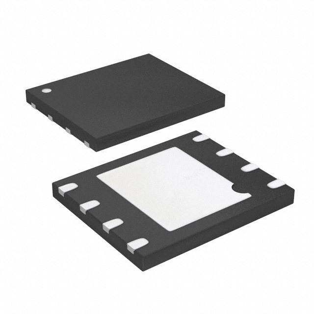
| 描述 | IC EEPROM 4KBIT 2MHZ 8SOIC电可擦除可编程只读存储器 4K (512x8/256x16) 3-WIRE, NiPdAu, 1.7V |
| 产品分类 | |
| 品牌 | Atmel |
| 产品手册 | |
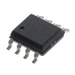
| 产品图片 |
|
| rohs | 符合RoHS无铅 / 符合限制有害物质指令(RoHS)规范要求 |
| 产品系列 | 内存,电可擦除可编程只读存储器,Atmel AT93C66B-SSHM-T- |
| 数据手册 | |
| 产品型号 | AT93C66B-SSHM-T |
| 产品种类 | 电可擦除可编程只读存储器 |
| 供应商器件封装 | 8-SOIC |
| 其它名称 | AT93C66B-SSHM-TCT |
| 包装 | 剪切带 (CT) |
| 商标 | Atmel |
| 存储器类型 | EEPROM |
| 存储容量 | 4 kbit |
| 安装风格 | SMD/SMT |
| 封装 | Reel |
| 封装/外壳 | 8-SOIC(0.154",3.90mm 宽) |
| 封装/箱体 | SOIC-8 |
| 工作温度 | -40°C ~ 85°C |
| 工作电流 | 0.5 mA |
| 工作电源电压 | 1.7 V to 5.5 V |
| 工厂包装数量 | 4000 |
| 接口 | Microwire 3 线串行 |
| 接口类型 | Serial (3-Wire) |
| 数据保留 | 100 yr |
| 最大工作温度 | + 85 C |
| 最大工作电流 | 2 mA |
| 最大时钟频率 | 2 MHz |
| 最小工作温度 | - 40 C |
| 标准包装 | 1 |
| 格式-存储器 | EEPROMs - 串行 |
| 电压-电源 | 1.7 V ~ 5.5 V |
| 电源电压-最大 | 5.5 V |
| 电源电压-最小 | 1.7 V |
| 组织 | 512 x 8, 256 x 16 |
| 速度 | 250kHz,1MHz,2MHz |


- 商务部:美国ITC正式对集成电路等产品启动337调查
- 曝三星4nm工艺存在良率问题 高通将骁龙8 Gen1或转产台积电
- 太阳诱电将投资9.5亿元在常州建新厂生产MLCC 预计2023年完工
- 英特尔发布欧洲新工厂建设计划 深化IDM 2.0 战略
- 台积电先进制程称霸业界 有大客户加持明年业绩稳了
- 达到5530亿美元!SIA预计今年全球半导体销售额将创下新高
- 英特尔拟将自动驾驶子公司Mobileye上市 估值或超500亿美元
- 三星加码芯片和SET,合并消费电子和移动部门,撤换高东真等 CEO
- 三星电子宣布重大人事变动 还合并消费电子和移动部门
- 海关总署:前11个月进口集成电路产品价值2.52万亿元 增长14.8%


_renders/IS45S16100H-7TLA1.jpg)

PDF Datasheet 数据手册内容提取
AT93C56B and AT93C66B 3-wire Serial EEPROM 2K (256 x 8 or 128 x 16) and 4K (512 x 8 or 256 x 16) DATASHEET Features Low-voltage Operation ̶ V = 1.7V to 5.5V CC User-selectable Internal Organization ̶ 2K: 256 x 8 or 128 x 16 ̶ 4K: 512 x 8 or 256 x 16 3-wire Serial Interface Sequential Read Operation 2MHz Clock Rate (5V) Self-timed Write Cycle (5ms Max) High Reliability ̶ Endurance: 1,000,000 Write Cycles ̶ Data Retention: 100 Years 8-lead JEDEC SOIC, 8-lead TSSOP, 8-pad UDFN, 8-pad XDFN, and 8-ball VFBGA packages Description The Atmel® AT93C56B/66B provides 2,048/4,096 bits of Serial Electrically Erasable Programmable Read-Only Memory (EEPROM) organized as 128/256 words of 16 bits each (when the ORG pin is connected to V ) and 256/512 words CC of 8 bits each (when the ORG pin is tied to ground). The device is optimized for use in many industrial and commercial applications where low-power and low- voltage operations are essential. The AT93C56B/66B is available in space-saving 8-lead JEDEC SOIC, 8-lead TSSOP, 8-pad UDFN, 8-pad XDFN, and 8-ball VFBGA packages. The AT93C56B/66B is enabled through the Chip Select pin (CS) and accessed via a 3-wire serial interface consisting of Data Input (DI), Data Output (DO), and Shift Clock (SK). Upon receiving a Read instruction at DI, the address is decoded, and the data is clocked out serially on the DO pin. The write cycle is completely self-timed, and no separate erase cycle is required before Write. The write cycle is only enabled when the part is in the Erase/Write Enable state. When CS is brought high following the initiation of a write cycle, the DO pin outputs the Ready/Busy status of the part. The AT93C56B/66B operates from 1.7V to 5.5V. Atmel-8735C-SEEPROM-AT93C56B-66B-Datasheet_012015
1. Pin Configurations and Pinouts Table 1-1. Pin Configurations 8-lead SOIC 8-lead TSSOP Pin Name Function CS Chip Select CS 1 8 VCC CS 1 8 VCC SK 2 7 NC SK 2 7 NC SK Serial Data Clock DI 3 6 ORG DI 3 6 ORG DO 4 5 GND DI Serial Data Input DO 4 5 GND Top View DO Serial Data Output Top View GND Ground V Power Supply CC 8-pad UDFN/XDFN 8-ball VFBGA ORG Internal Organization VCC 8 1 CS VCC 8 1 CS NC No Connect NC 7 2 SK NC 7 2 SK ORG 6 3 DI ORG 6 3 DI GND 5 4 DO GND 5 4 DO Bottom View Bottom View Note: Drawings are not to scale. 2. Absolute Maximum Ratings* Operating Temperature55C to +125C *Notice: Stresses beyond those listed under “Absolute Maximum Ratings” may cause permanent damage Storage Temperature65C to +150C to the device. This is a stress rating only, and functional operation of the device at these or any Voltage on any pin other conditions beyond those indicated in the with respect to ground1.0V to +7.0V operational sections of this specification is not implied. Exposure to absolute maximum rating Maximum Operating Voltage . . . . . . . . . . . . . . . 6.25V conditions for extended periods may affect device DC Output Current. . . . . . . . . . . . . . . . . . . . . . .5.0mA reliability. 2 AT93C56B/66B [DATASHEET] Atmel-8735C-SEEPROM-AT93C56B-66B-Datasheet_012015
3. Block Diagram V GND CC Memory Array Address 256/512 x 8 ORG Decoder or 128/256 x 16 Data Register DI Output Buffer Mode Decode Logic CS Clock SK DO Generator Note: When the ORG pin is connected to V , the x16 organization is selected. When it is connected to ground, CC the x8 organization is selected. If the ORG pin is left unconnected, and the application does not load the input beyond the capability of the internal 1M pull-up resistor, then the x16 organization is selected. AT93C56B/66B [DATASHEET] 3 Atmel-8735C-SEEPROM-AT93C56B-66B-Datasheet_012015
4. Memory Organization 4.1 Pin Capacitance(1) Applicable over recommended operating range from T = 25C, f = 1.0MHz, V = 5.0V (unless otherwise noted). A CC Symbol Test Conditions Max Units Conditions C Output Capacitance (DO) 5 pF V = 0V OUT OUT C Input Capacitance (CS, SK, DI) 5 pF V = 0V IN IN Note: 1. This parameter is characterized, and is not 100% tested. 4.2 DC Characteristics Applicable over recommended operating range from T = -40°C to +85°C, V = 1.7V to 5.5V (unless otherwise noted). AI CC Symbol Parameter Test Condition Min Typ Max Unit V Supply Voltage 1.7 5.5 V CC1 V Supply Voltage 2.5 5.5 V CC2 V Supply Voltage 4.5 5.5 V CC3 Read at 1.0MHz 0.5 2.0 mA I Supply Current V = 5.0V CC CC Write at 1.0MHz 0.5 2.0 mA I Standby Current V = 1.7V CS = 0V 0.4 1.0 μA SB1 CC I Standby Current V = 2.5V CS = 0V 6.0 10.0 μA SB2 CC I Standby Current V = 5.0V CS = 0V 10.0 15.0 μA SB3 CC I Input Leakage V = 0V to V 0.1 3.0 μA IL IN CC I Output Leakage V = 0V to V 0.1 3.0 μA OL IN CC V (1) Input Low Voltage 2.5V V 5.5V 0.6 0.8 V IL1 CC V (1) Input High Voltage 2.5V V 5.5V 2.0 V + 1 V IH1 CC CC V (1) Input Low Voltage 1.7V V 2.5V 0.6 V x 0.3 V IL2 CC CC V (1) Input High Voltage 1.7V V 2.5V V x 0.7 V + 1 V IH2 CC CC CC V Output Low Voltage 2.5V V 5.5V I = 2.1mA 0.4 V OL1 CC OL V Output High Voltage 2.5V V 5.5V I = 0.4mA 2.4 V OH1 CC OH V Output Low Voltage 1.7V V 2.5V I = 0.15mA 0.2 V OL2 CC OL V Output High Voltage 1.7V V 2.5V I = 100μA V 0.2 V OH2 CC OH CC Note: 1. V min and V max are reference only, and are not tested. IL IH 4 AT93C56B/66B [DATASHEET] Atmel-8735C-SEEPROM-AT93C56B-66B-Datasheet_012015
4.3 AC Characteristics Applicable over recommended operating range from T = -40°C to + 85°C, V = as specified, CL = 1 TTL gate and 100pF AI CC (unless otherwise noted). Symbol Parameter Test Condition Min Max Units 4.5V V 5.5V 0 2 MHz CC f SK Clock Frequency 2.5V V 5.5V 0 1 MHz SK CC 1.7V V 5.5V 0 250 kHz CC 2.5V V 5.5V 250 ns CC t SK High Time SKH 1.7V V 5.5V 1000 ns CC 2.5V V 5.5V 250 ns CC t SK Low Time SKL 1.7V V 5.5V 1000 ns CC 2.5V V 5.5V 250 ns CC t Minimum CS Low Time CS 1.7V V 5.5V 1000 ns CC 2.5V V 5.5V 50 ns CC t CS Setup Time Relative to SK CSS 1.7V V 5.5V 200 ns CC 2.5V V 5.5V 100 ns CC t DI Setup Time Relative to SK DIS 1.7V V 5.5V 400 ns CC t CS Hold Time Relative to SK 0 ns CSH 2.5V V 5.5V 100 ns CC t DI Hold Time Relative to SK DIH 1.7V V 5.5V 400 ns CC 2.5V V 5.5V 250 ns CC t Output Delay to 1 AC Test PD1 1.7V V 5.5V 1000 ns CC 2.5V V 5.5V 250 ns CC t Output Delay to 0 AC Test PD0 1.7V V 5.5V 1000 ns CC 2.5V V 5.5V 250 ns CC t CS to Status Valid AC Test SV 1.7V V 5.5V 1000 ns CC AC Test 2.5V V 5.5V 150 ns CS to DO in CC t DF High-impedance CS = V 1.7V V 5.5V 400 ns IL CC t Write Cycle Time 1.7V V 5.5V 5 ms WP CC Endurance(1) 5.0V, 25°C 1,000,000 Write Cycles Note: 1. This parameter is characterized, and is not 100% tested. AT93C56B/66B [DATASHEET] 5 Atmel-8735C-SEEPROM-AT93C56B-66B-Datasheet_012015
5. Functional Description The AT93C56B/66B is accessed via a simple and versatile 3-wire serial communication interface. Device operation is controlled by seven instructions issued by the Host processor. A valid instruction starts with a rising edge of CS and consists of a Start bit (Logic 1), followed by the appropriate opcode, and the desired memory address location. Table 5-1. AT93C56B/66B Instruction Set Address Data Instruction SB Opcode x8(1) x16(1) x8 x16 Comments Reads data stored in memory at READ 1 10 A – A A – A 8 0 7 0 specified address. Write Enable must precede all EWEN 1 00 11XXXXXXX 11XXXXXX programming modes. ERASE 1 11 A – A A – A Erases memory location A – A . 8 0 7 0 N 0 WRITE 1 01 A – A A – A D – D D – D Writes memory location A – A . 8 0 7 0 7 0 15 0 N 0 Erases all memory locations. ERAL 1 00 10XXXXXXX 10XXXXXX Valid only at V (Section 4.2, “DC CC3 Characteristics” on page 4). Writes all memory locations. WRAL 1 00 01XXXXXXX 01XXXXXX D – D D – D Valid only at V (Section 4.2) and 7 0 15 0 CC3 Disable Register cleared. Disables all programming EWDS 1 00 00XXXXXXX 00XXXXXX instructions. Note: 1. The Xs in the address field represent don’t care values, and must be clocked. READ: The READ instruction contains the address code for the memory location to be read. After the instruction and address are decoded, data from the selected memory location is available at the Serial Output pin, DO. Output data changes are synchronized with the rising edges of the Serial Clock pin, SK. It should be noted that a dummy bit (Logic 0) precedes the 8-bit or 16-bit data output string. The AT93C56B/66B supports sequential Read operations. The device will automatically increment the internal address pointer and clock out the next memory location as long as Chip Select (CS) is held high. In this case, the dummy bit (Logic 0) will not be clocked out between memory locations, thus allowing for a continuous stream of data to be read. Erase/Write Enable (EWEN): To ensure data integrity, the part automatically goes into the Erase/Write Disable (EWDS) state when power is first applied. An Erase/Write Enable (EWEN) instruction must be executed first before any programming instructions can be carried out. Note: Once in the EWEN state, programming remains enabled until an EWDS instruction is executed, or V CC power is removed from the part. 6 AT93C56B/66B [DATASHEET] Atmel-8735C-SEEPROM-AT93C56B-66B-Datasheet_012015
ERASE: The ERASE instruction programs all bits in the specified memory location to the Logic 1 state. The self- timed erase cycle starts once the ERASE instruction and address are decoded. The DO pin outputs the Ready/Busy status of the part if CS is brought high after being kept low for a minimum of t . A Logic 1 at the CS DO pin indicates that the selected memory location has been erased, and the part is ready for another instruction. WRITE: The WRITE instruction contains the 8-bits or 16-bits of data to be written into the specified memory location. The self-timed programming cycle, t , starts after the last bit of data is received at Serial Data Input WP pin DI. The DO pin outputs the Ready/Busy status of the part if CS is brought high after being kept low for a minimum of t . A CS Logic 0 at DO indicates that programming is still in progress. A Logic 1 indicates that the memory location at the specified address has been written with the data pattern contained in the instruction, and the part is ready for further instructions. A Ready/Busy status cannot be obtained if CS is brought high after the end of the self-timed programming cycle, t . WP Erase All (ERAL): The Erase All (ERAL) instruction programs every bit in the Memory Array to the Logic 1 state and is primarily used for testing purposes. The DO pin outputs the ready/busy status of the part if CS is brought high after being kept low for a minimum of t . The ERAL instruction is valid only at V (Section 4.2, “DC CS CC3 Characteristics” on page 4). Write All (WRAL): The Write All (WRAL) instruction programs all memory locations with the data patterns specified in the instruction. The DO pin outputs the Ready/Busy status of the part if CS is brought high after being kept low for a minimum of t . The WRAL instruction is valid only at V (Section 4.2). CS CC3 Erase/Write Disable (EWDS): To protect against accidental data disturbance, the Erase/Write Disable (EWDS) instruction disables all programming modes and should be executed after all programming operations. The operation of the Read instruction is independent of both the EWEN and EWDS instructions and can be executed at any time. AT93C56B/66B [DATASHEET] 7 Atmel-8735C-SEEPROM-AT93C56B-66B-Datasheet_012015
6. Timing Diagrams Figure 6-1. Synchronous Data Timing V IH CS V IL tCSS tSKH tSKL tCSH V IH SK V IL tDIS tDIH V IH DI V IL tPD0 tPD1 tDF V OH DO (Read) V OL tSV tDF V OH DO (Program) Status Valid V OL Table 6-1. Organization Key for Timing Diagrams AT93C56B (2K) AT93C66B (4K) I/O x8 x16 x8 x16 A A (1) A (2) A A N 8 7 8 7 D D D D D N 7 15 7 15 Notes: 1. A is a don’t-care value, but the extra clock is required. 8 2. A is a don’t-care value, but the extra clock is required. 7 Figure 6-2. READ Timing CS tCS SK DI 1 1 0 AN A0 High-impedance DO 0 DN D0 8 AT93C56B/66B [DATASHEET] Atmel-8735C-SEEPROM-AT93C56B-66B-Datasheet_012015
Figure 6-3. EWEN Timing CS tCS SK DI 1 0 0 1 1 ... Figure 6-4. ERASE Timing tCS CS Check Standby Status SK DI 1 1 1 AN AN-1 AN-2 ... A0 tSV tDF High-impedance High-impedance DO Busy Ready tWP Figure 6-5. WRITE Timing CS tCS SK DI 1 0 1 AN ... A0 DN ... D0 High-impedance DO Busy Ready tWP AT93C56B/66B [DATASHEET] 9 Atmel-8735C-SEEPROM-AT93C56B-66B-Datasheet_012015
Figure 6-6. ERAL Timing(1) tCS CCSS Check Standby Status SSKK DDII 1 0 0 1 0 tSV tDF High-impedance High-impedance DDOO Busy Ready tWP Note: 1. Valid only at V (Section 4.2). CC3 Figure 6-7. WRAL Timing(1) tCS CCSS SSKK DDII 1 0 0 0 1 ... DN ... D0 High-impedance DDOO Busy Ready tWP Note: 1. Valid only at V (Section 4.2). CC3 Figure 6-8. EWDS Timing CS tCS SK DI 1 0 0 0 0 ... 10 AT93C56B/66B [DATASHEET] Atmel-8735C-SEEPROM-AT93C56B-66B-Datasheet_012015
7. Ordering Code Detail A T 9 3 C 5 6 B - S S H M - B Atmel Designator Shipping Carrier Option B or Blank = Bulk (Tubes) T = Tape and Reel, Standard Quantity Option E = Tape and Reel, Expanded Quantity Option Product Family 93C = Microwire-compatible 3-Wire Serial EEPROM Operating Voltage M = 1.7V to 5.5V Device Density 56 = 2k Package Device Grade or 66 = 4k Wafer/Die Thickness H = Green, NiPdAu Lead Finish Industrial Temperature Range Device Revision (-40°C to +85°C) U = Green, Matte Sn Lead Finish Industrial Temperature Range (-40°C to +85°C) 11 = 11mil Wafer Thickness Package Option SS = JEDEC SOIC X = TSSOP MA = UDFN ME = XDFN C = VFBGA WWU = Wafer Unsawn AT93C56B/66B [DATASHEET] 11 Atmel-8735C-SEEPROM-AT93C56B-66B-Datasheet_012015
8. Ordering Information Delivery Information Operation Atmel Ordering Code Lead Finish Package Form Quantity Range AT93C56B-SSHM-B Bulk (Tubes) 100 per Tube 8S1 AT93C56B-SSHM-T Tape and Reel 4,000 per Reel AT93C56B-XHM-B Bulk (Tubes) 100 per Tube 8X NiPdAu AT93C56B-XHM-T Tape and Reel 5,000 per Reel (Lead-free/Halogen-free) Industrial AT93C56B-MAHM-T Tape and Reel 5,000 per Reel Temperature 8MA2 (-40C to 85C) AT93C56B-MAHM-E Tape and Reel 15,000 per Reel AT93C56B-MEHM-T 8ME1 Tape and Reel 5,000 per Reel SnAgCu AT93C56B-CUM-T 8U3-1 Tape and Reel 5,000 per Reel (Lead-free/Halogen-free) AT93C56B-WWU11M(1) N/A Wafer Sale Note 1 AT93C66B-SSHM-B Bulk (Tubes) 100 per Tube 8S1 AT93C66B-SSHM-T Tape and Reel 4,000 per Reel AT93C66B-XHM-B Bulk (Tubes) 100 per Tube 8X NiPdAu AT93C66B-XHM-T Tape and Reel 5,000 per Reel (Lead-free/Halogen-free) Industrial AT93C66B-MAHM-T Tape and Reel 5,000 per Reel Temperature 8MA2 (-40C to 85C) AT93C66B-MAHM-E Tape and Reel 15,000 per Reel AT93C66B-MEHM-T 8ME1 Tape and Reel 5,000 per Reel SnAgCu AT93C66B-CUM-T 8U3-1 Tape and Reel 5,000 per Reel (Lead-free/Halogen-free) AT93C66B-WWU11M(1) N/A Wafer Sale Note 1 Note: 1. For wafer sales, please contact Atmel sales. Package Type 8S1 8-lead, 0.150” wide, Plastic Gull Wing, Small Outline (JEDEC SOIC) 8X 8-lead, 0.170” wide, Thin Shrink Small Outline (TSSOP) 8MA2 8-pad, 2.00mm x 3.00mm body, 0.50mm pitch, Ultra Thin Dual No Lead (UDFN) 8ME1 8-pad, 1.80mm x 2.20mm body, Extra Thin Dual No Lead (XDFN) 8U3-1 8-ball, 1.50mm x 2.00mm body, 0.50mm pitch, Small Die Ball Grid Array (VFBGA) 12 AT93C56B/66B [DATASHEET] Atmel-8735C-SEEPROM-AT93C56B-66B-Datasheet_012015
9. Part Markings AT93C56B and AT93C66B: Package Marking Information 8-lead SOIC 8-lead TSSOP 8-pad UDFN 2.0 x 3.0 mm Body ATHYWW ### ATMLHYWW ###% @ ###% @ H%@ AAAAAAAA AAAAAAA YXX 8-pad XDFN 8-ball VFBGA 1.8 x 2.2 mm Body 1.5 x 2.0 mm Body ### ###U YXX YMXX PIN 1 Note 1: designates pin 1 Note 2: Package drawings are not to scale Catalog Number Truncation AT93C56B Truncation Code ###: 56B AT93C66B Truncation Code ###: 66B Date Codes Voltages Y = Year M = Month WW = Work Week of Assembly % = Minimum Voltage 3: 2013 7: 2017 A: January 02: Week 2 M: 1.7V min 4: 2014 8: 2018 B: February 04: Week 4 5: 2015 9: 2019 ... ... 6: 2016 0: 2020 L: December 52: Week 52 Country of Assembly L ot Number Grade/Lead Finish Material @ = Country of Assembly AAA...A = Atmel Wafer Lot Number U: Industrial/Matte Tin/SnAgCu H: Industrial/NiPdAu Trace Code Atmel Truncation XX = Trace Code (Atmel Lot Numbers Correspond to Code) AT: Atmel Example: AA, AB.... YZ, ZZ ATM: Atmel ATML: Atmel 3/22/13 TITLE DRAWING NO. REV. 93C56-66BSM, AT93C56B and AT93C66B Package Marking Package Mark Contact: Information 93C56-66BSM B DL-CSO-Assy_eng@atmel.com AT93C56B/66B [DATASHEET] 13 Atmel-8735C-SEEPROM-AT93C56B-66B-Datasheet_012015
10. Packaging Information 10.1 8S1 — 8-lead JEDEC SOIC C 1 E E1 L N Ø TOP VIEW END VIEW e b A COMMON DIMENSIONS (Unit of Measure = mm) SYMBOL MIN NOM MAX NOTE A1 A 1.35 – 1.75 A1 0.10 – 0.25 b 0.31 – 0.51 C 0.17 – 0.25 D 4.80 – 5.05 D E1 3.81 – 3.99 E 5.79 – 6.20 SIDE VIEW e 1.27 BSC Notes: This drawing is for general information only. L 0.40 – 1.27 Refer to JEDEC Drawing MS-012, Variation AA ØØ 0° – 8° for proper dimensions, tolerances, datums, etc. 6/22/11 TITLE GPC DRAWING NO. REV. 8S1, 8-lead (0.150” Wide Body), Plastic Gull Wing SWB 8S1 G Package Drawing Contact: Small Outline (JEDEC SOIC) packagedrawings@atmel.com 14 AT93C56B/66B [DATASHEET] Atmel-8735C-SEEPROM-AT93C56B-66B-Datasheet_012015
10.2 8X — 8-lead TSSOP C 1 Pin 1 indicator this corner E1 E L1 N L Top View End View A b A1 COMMON DIMENSIONS e A2 (Unit of Measure = mm) D SYMBOL MIN NOM MAX NOTE Side View A - - 1.20 A1 0.05 - 0.15 Notes: 1. This drawing is for general information only. A2 0.80 1.00 1.05 Refer to JEDEC Drawing MO-153, Variation AA, for proper dimensions, tolerances, datums, etc. D 2.90 3.00 3.10 2, 5 2. Dimension D does not include mold Flash, protrusions or gate E 6.40 BSC burrs. Mold Flash, protrusions and gate burrs shall not exceed 0.15mm (0.006in) per side. E1 4.30 4.40 4.50 3, 5 3. Dimension E1 does not include inter-lead Flash or protrusions. Inter-lead Flash and protrusions shall not exceed 0.25mm b 0.19 0.25 0.30 4 (0.010in) per side. e 0.65 BSC 4. Dimension b does not include Dambar protrusion. Allowable Dambar protrusion shall be 0.08mm total in excess L 0.45 0.60 0.75 of the b dimension at maximum material condition. Dambar L1 1.00 REF cannot be located on the lower radius of the foot. Minimum space between protrusion and adjacent lead is 0.07mm. C 0.09 - 0.20 5. Dimension D and E1 to be determined at Datum Plane H. 2/27/14 TITLE GPC DRAWING NO. REV. 8X, 8-lead 4.4mm Body, Plastic Thin Package Drawing Contact: Shrink Small Outline Package (TSSOP) TNR 8X E packagedrawings@atmel.com AT93C56B/66B [DATASHEET] 15 Atmel-8735C-SEEPROM-AT93C56B-66B-Datasheet_012015
10.3 8MA2 — 8-pad UDFN E 1 8 Pin 1 ID 2 7 D 3 6 4 5 TOP VIEW C SIDE VIEW A2 A A1 E2 b (8x) 8 1 COMMON DIMENSIONS 7 2 Pin#1 ID (Unit of Measure = mm) D2 6 3 SYMBOL MIN NOM MAX NOTE A 0.50 0.55 0.60 5 4 A1 0.0 0.02 0.05 e (6x) A2 - - 0.55 L (8x) K D 1.90 2.00 2.10 BOTTOM VIEW D2 1.40 1.50 1.60 Notes: 1. This drawing is for general information only. Refer to E 2.90 3.00 3.10 Drawing MO-229, for proper dimensions, tolerances, E2 1.20 1.30 1.40 datums, etc. 2. The Pin #1 ID is a laser-marked feature on Top View. b 0.18 0.25 0.30 3 3. Dimensions b applies to metallized terminal and is C 1.52 REF measured between 0.15 mm and 0.30 mm from the terminal tip. If the terminal has the optional radius on L 0.30 0.35 0.40 the other end of the terminal, the dimension should e 0.50 BSC not be measured in that radius area. 4. The Pin #1 ID on the Bottom View is an orientation K 0.20 - - feature on the thermal pad. 11/26/14 TITLE GPC DRAWING NO. REV. 8MA2, 8-pad 2 x 3 x 0.6mm Body, Thermally Package Drawing Contact: Enhanced Plastic Ultra Thin Dual Flat No-Lead YNZ 8MA2 G packagedrawings@atmel.com Package (UDFN) 16 AT93C56B/66B [DATASHEET] Atmel-8735C-SEEPROM-AT93C56B-66B-Datasheet_012015
10.4 8ME1 — 8-pad XDFN D 8 7 6 5 PIN #1 ID E 1 2 3 4 A1 Top View A Side View e1 b L COMMON DIMENSIONS (Unit of Measure = mm) SYMBOL MIN NOM MAX NOTE 0.10 A – – 0.40 PIN #1 ID A1 0.00 – 0.05 D 1.70 1.80 1.90 0.15 E 2.10 2.20 2.30 b 0.15 0.20 0.25 b e 0.40 TYP e e1 1.20 REF L 0.26 0.30 0.35 End View 9/10/2012 TITLE GPC DRAWING NO. REV. 8ME1, 8-pad (1.80mm x 2.20mm body) DTP 8ME1 B Package Drawing Contact: Extra Thin DFN (XDFN) packagedrawings@atmel.com AT93C56B/66B [DATASHEET] 17 Atmel-8735C-SEEPROM-AT93C56B-66B-Datasheet_012015
10.5 8U3-1 — 8-ball VFBGA E D 2. b PIN 1 BALL PAD CORNER A1 A2 TOP VIEW A SIDE VIEW PIN 1 BALL PAD CORNER 1 2 3 4 d (d1) 8 7 6 5 e COMMON DIMENSIONS (Unit of Measure - mm) (e1) SYMBOL MIN NOM MAX NOTE BOTTOM VIEW A 0.73 0.79 0.85 8 SOLDER BALLS A1 0.09 0.14 0.19 A2 0.40 0.45 0.50 Notes: b 0.20 0.25 0.30 2 1. This drawing is for general information only. D 1.50 BSC E 2.0 BSC 2. Dimension ‘b’ is measured at maximum solder ball diameter. e 0.50 BSC 3. Solder ball composition shall be 95.5Sn-4.0Ag-.5Cu. e1 0.25 REF d 1.00 BSC d1 0.25 REF 6/11/13 TITLE GPC DRAWING NO. REV. 8U3-1, 8-ball, 1.50mm x 2.00mm body, 0.50mm pitch, Package Drawing Contact: Very Thin, Fine-Pitch Ball Grid Array Package (VFBGA) GXU 8U3-1 F packagedrawings@atmel.com 18 AT93C56B/66B [DATASHEET] Atmel-8735C-SEEPROM-AT93C56B-66B-Datasheet_012015
11. Revision History Rev. No. Date Comments Add the UDFN extended quantity option and update package outline drawings. 8735C 01/2015 Update the 8MA2 package drawing. Correct Synchronous Data Timing figure and remove note. Update TSSOP package option from 8A2 to 8X. 8735B 04/2013 Update UDFN package option from 8Y6 to 8MA2. Update template and Atmel logos. 8735A 01/2011 Initial document release. AT93C56B/66B [DATASHEET] 19 Atmel-8735C-SEEPROM-AT93C56B-66B-Datasheet_012015
X X X X X X Atmel Corporation 1600 Technology Drive, San Jose, CA 95110 USA T: (+1)(408) 441.0311 F: (+1)(408) 436.4200 | www.atmel.com © 2015 Atmel Corporation. / Rev.: Atmel-8735C-SEEPROM-AT93C56B-66B-Datasheet_012015. Atmel®, Atmel logo and combinations thereof, Enabling Unlimited Possibilities®, and others are registered trademarks or trademarks of Atmel Corporation in U.S. and other countries. Other terms and product names may be trademarks of others. DISCLAIMER: The information in this document is provided in connection with Atmel products. No license, express or implied, by estoppel or otherwise, to any intellectual property right is granted by this document or in connection with the sale of Atmel products. EXCEPT AS SET FORTH IN THE ATMEL TERMS AND CONDITIONS OF SALES LOCATED ON THE ATMEL WEBSITE, ATMEL ASSUMES NO LIABILITY WHATSOEVER AND DISCLAIMS ANY EXPRESS, IMPLIED OR STATUTORY WARRANTY RELATING TO ITS PRODUCTS INCLUDING, BUT NOT LIMITED TO, THE IMPLIED WARRANTY OF MERCHANTABILITY, FITNESS FOR A PARTICULAR PURPOSE, OR NON-INFRINGEMENT. IN NO EVENT SHALL ATMEL BE LIABLE FOR ANY DIRECT, INDIRECT, CONSEQUENTIAL, PUNITIVE, SPECIAL OR INCIDENTAL DAMAGES (INCLUDING, WITHOUT LIMITATION, DAMAGES FOR LOSS AND PROFITS, BUSINESS INTERRUPTION, OR LOSS OF INFORMATION) ARISING OUT OF THE USE OR INABILITY TO USE THIS DOCUMENT, EVEN IF ATMEL HAS BEEN ADVISED OF THE POSSIBILITY OF SUCH DAMAGES. Atmel makes no representations or warranties with respect to the accuracy or completeness of the contents of this document and reserves the right to make changes to specifications and products descriptions at any time without notice. Atmel does not make any commitment to update the information contained herein. Unless specifically provided otherwise, Atmel products are not suitable for, and shall not be used in, automotive applications. Atmel products are not intended, authorized, or warranted for use as components in applications intended to support or sustain life. SAFETY-CRITICAL, MILITARY, AND AUTOMOTIVE APPLICATIONS DISCLAIMER: Atmel products are not designed for and will not be used in connection with any applications where the failure of such products would reasonably be expected to result in significant personal injury or death (“Safety-Critical Applications”) without an Atmel officer's specific written consent. Safety-Critical Applications include, without limitation, life support devices and systems, equipment or systems for the operation of nuclear facilities and weapons systems. Atmel products are not designed nor intended for use in military or aerospace applications or environments unless specifically designated by Atmel as military-grade. Atmel products are not designed nor intended for use in automotive applications unless specifically designated by Atmel as automotive-grade.
Mouser Electronics Authorized Distributor Click to View Pricing, Inventory, Delivery & Lifecycle Information: M icrochip: AT93C56B-MAHM-T AT93C56B-SSHM-B AT93C56B-SSHM-T AT93C56B-XHM-B AT93C56B-XHM-T AT93C66B- MAHM-T AT93C66B-XHM-B AT93C66B-SSHM-B AT93C66B-XHM-T AT93C66B-SSHM-T AT93C56B-MAHM-E AT93C66B-MAHM-E AT93C66B-XPD-T