ICGOO在线商城 > 集成电路(IC) > 嵌入式 - 微控制器 > AT91SAM9RL64-CU
 Datasheet下载
- 型号: AT91SAM9RL64-CU
- 制造商: Atmel
- 库位|库存: xxxx|xxxx
- 要求:
| 数量阶梯 | 香港交货 | 国内含税 |
| +xxxx | $xxxx | ¥xxxx |
查看当月历史价格
查看今年历史价格
AT91SAM9RL64-CU产品简介:
ICGOO电子元器件商城为您提供AT91SAM9RL64-CU由Atmel设计生产,在icgoo商城现货销售,并且可以通过原厂、代理商等渠道进行代购。 AT91SAM9RL64-CU价格参考。AtmelAT91SAM9RL64-CU封装/规格:嵌入式 - 微控制器, ARM926EJ-S 微控制器 IC SAM9R 16/32-位 240MHz 32KB(32K x 8) ROM 217-LFBGA(15x15)。您可以下载AT91SAM9RL64-CU参考资料、Datasheet数据手册功能说明书,资料中有AT91SAM9RL64-CU 详细功能的应用电路图电压和使用方法及教程。
Microchip Technology的AT91SAM9RL64-CU是一款嵌入式微控制器,主要应用于工业控制、消费电子、医疗设备、通信系统和汽车电子等领域。这款微控制器基于ARM926EJ-S内核,具有高性能、低功耗和丰富的外设接口等特点,适用于多种应用场景。

1. 工业控制:AT91SAM9RL64-CU可用于工业自动化系统中,如PLC(可编程逻辑控制器)、HMI(人机界面)和运动控制系统。其高处理能力和丰富的外设接口(如UART、SPI、I2C等)使得它能够高效地处理复杂的工业协议和实时数据传输。

2. 消费电子:在消费电子产品中,该微控制器可用于智能家电、智能家居网关和其他物联网设备。它支持多种通信接口,如以太网、USB和SD卡接口,方便与外部设备进行数据交换,同时其低功耗特性有助于延长电池寿命。

3. 医疗设备:在医疗领域,AT91SAM9RL64-CU可用于便携式医疗设备、监护仪和诊断仪器。其内置的ADC(模数转换器)和PWM(脉宽调制)功能可以用于采集生理信号和控制外部设备,而其强大的处理能力则可以实现复杂的数据分析和算法处理。

4. 通信系统:该微控制器适合用于通信终端设备,如路由器、网关和无线模块。它支持以太网接口,便于构建网络连接,并且可以通过USB和UART等接口与其他通信设备进行交互,确保数据的可靠传输。

5. 汽车电子:在汽车应用中,AT91SAM9RL64-CU可用于车载信息娱乐系统、车身控制模块和驾驶辅助系统。其高可靠性和低功耗特性使其能够在严苛的汽车环境中稳定工作,同时其丰富的外设接口也方便与其他汽车电子模块集成。

总之,AT91SAM9RL64-CU凭借其高性能、低功耗和丰富的外设接口,在多个领域都有着广泛的应用前景。
| 参数 | 数值 |
| A/D位大小 | 10 bit |
| 产品目录 | 集成电路 (IC)半导体 |
| 描述 | IC MCU ARM9 32KB ROM 217LFBGAARM微控制器 - MCU ARM Thumb MCU |
| EEPROM容量 | - |
| 产品分类 | |
| I/O数 | 118 |
| 品牌 | Atmel |
| 产品手册 | |
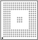
| 产品图片 |
|
| rohs | 符合RoHS无铅 / 符合限制有害物质指令(RoHS)规范要求 |
| 产品系列 | 嵌入式处理器和控制器,微控制器 - MCU,ARM微控制器 - MCU,Atmel AT91SAM9RL64-CUSAM9R |
| 数据手册 | |
| 产品型号 | AT91SAM9RL64-CU |
| RAM容量 | 72K x 8 |
| 产品培训模块 | http://www.digikey.cn/PTM/IndividualPTM.page?site=cn&lang=zhs&ptm=24723http://www.digikey.cn/PTM/IndividualPTM.page?site=cn&lang=zhs&ptm=24997http://www.digikey.cn/PTM/IndividualPTM.page?site=cn&lang=zhs&ptm=26162http://www.digikey.cn/PTM/IndividualPTM.page?site=cn&lang=zhs&ptm=26159http://www.digikey.cn/PTM/IndividualPTM.page?site=cn&lang=zhs&ptm=26180 |
| 产品种类 | ARM微控制器 - MCU |
| 供应商器件封装 | * |
| 其它名称 | AT91SAM9RL64CU |
| 包装 | 托盘 |
| 可用A/D通道 | 6 |
| 可编程输入/输出端数量 | 118 |
| 商标 | Atmel |
| 处理器系列 | AT91SAMx |
| 外设 | AC'97,LCD,POR,PWM,WDT |
| 安装风格 | SMD/SMT |
| 定时器数量 | 4 Timer |
| 封装/外壳 | 217-LFBGA |
| 封装/箱体 | LFBGA |
| 工作温度 | -40°C ~ 85°C |
| 工作电源电压 | 1.2 V, 3.3 V |
| 工厂包装数量 | 126 |
| 振荡器类型 | 内部 |
| 接口类型 | 2-Wire, SPI, SSC, USART |
| 数据RAM大小 | 64 kB |
| 数据总线宽度 | 32 bit |
| 数据转换器 | A/D 6x10b |
| 最大工作温度 | + 85 C |
| 最大时钟频率 | 240 MHz |
| 最小工作温度 | - 40 C |
| 标准包装 | 126 |
| 核心 | ARM926EJ |
| 核心处理器 | ARM9® |
| 核心尺寸 | 16/32-位 |
| 片上ADC | Yes |
| 电压-电源(Vcc/Vdd) | 1.65 V ~ 3.6 V |
| 程序存储器大小 | 32 kB |
| 程序存储器类型 | ROM |
| 程序存储容量 | 32KB(32K x 8) |
| 系列 | SAM9R |
| 输入/输出端数量 | 118 I/O |
| 连接性 | EBI/EMI, I²C, 存储器卡, SPI, SSC, UART/USART, USB |
| 速度 | 240MHz |
| 配用 | /product-detail/zh/AT91SAM9RL-EK/AT91SAM9RL-EK-ND/1802912/product-detail/zh/AT91SAM-ICE/AT91SAM-ICE-ND/1008639 |
| 长度 | 15 mm |


- 商务部:美国ITC正式对集成电路等产品启动337调查
- 曝三星4nm工艺存在良率问题 高通将骁龙8 Gen1或转产台积电
- 太阳诱电将投资9.5亿元在常州建新厂生产MLCC 预计2023年完工
- 英特尔发布欧洲新工厂建设计划 深化IDM 2.0 战略
- 台积电先进制程称霸业界 有大客户加持明年业绩稳了
- 达到5530亿美元!SIA预计今年全球半导体销售额将创下新高
- 英特尔拟将自动驾驶子公司Mobileye上市 估值或超500亿美元
- 三星加码芯片和SET,合并消费电子和移动部门,撤换高东真等 CEO
- 三星电子宣布重大人事变动 还合并消费电子和移动部门
- 海关总署:前11个月进口集成电路产品价值2.52万亿元 增长14.8%


PDF Datasheet 数据手册内容提取
Features • Incorporates the ARM926EJ-S™ ARM® Thumb® Processor – DSP Instruction Extensions – ARM Jazelle® Technology for Java® Acceleration – 4 Kbyte Data Cache, 4 Kbyte Instruction Cache, Write Buffer – 220 MIPS at 200 MHz – Memory Management Unit – EmbeddedICE™ In-circuit Emulation, Debug Communication Channel Support (cid:129) Multi-layer AHB Bus Matrix for Large Bandwidth Transfers AT91SAM – Six 32-bit-layer Matrix – Boot Mode Select Option, Remap Command ARM-based (cid:129) One 32-KByte internal ROM, Single-cycle Access at Maximum Speed (cid:129) One 64-KByte internal SRAM, Single-cycle Access at Maximum Speed Embedded MPU – 4 Blocks of 16 Kbytes Configurable in TCM or General-purpose SRAM on the AHB Bus Matrix – Single-cycle Accessible on AHB Bus at Bus Speed AT91SAM9R64 – Single-cycle Accessible on TCM Interface at Processor Speed (cid:129) 2-channel DMA AT91SAM9RL64 – Memory to Memory Transfer – 16 Bytes FIFO – LInked List (cid:129) External Bus Interface (EBI) – EBI Supports SDRAM, Static Memory, ECC-enabled NAND Flash and CompactFlash® (cid:129) LCD Controller (for AT91SAM9RL64 only) – Supports Passive or Active Displays – Up to 24 Bits per Pixel in TFT Mode, Up to 16 bits per Pixel in STN Color Mode – Up to 16M Colors in TFT Mode, Resolution Up to 2048x2048, Virtual Screen Support (cid:129) High Speed (480 Mbit/s) USB 2.0 Device Controller – On-Chip High Speed Transceiver, UTMI+ Physical Interface – Integrated FIFOs and Dedicated DMA – 4 Kbyte Configurable Integrated DPRAM (cid:129) Fully-featured System Controller, including – Reset Controller, Shutdown Controller – Four 32-bit Battery Backup Registers for a Total of 16 Bytes – Clock Generator and Power Management Controller – Advanced Interrupt Controller and Debug Unit – Periodic Interval Timer, Watchdog Timer and Real-time Timer and Real-time Clock (cid:129) Reset Controller (RSTC) – Based on Two Power-on Reset Cells – Reset Source Identification and Reset Output Control (cid:129) Shutdown Controller (SHDC) – Programmable Shutdown Pin Control and Wake-up Circuitry (cid:129) Clock Generator (CKGR) – Selectable 32768 Hz Low-power Oscillator or Internal Low-power RC Oscillator on Battery Backup Power Supply, Providing a Permanent Slow Clock – 12 MHz On-chip Oscillator for Main System Clock and USB Clock – One PLL up to 240 MHz 6289D–ATARM–3-Oct-11
– One PLL 480 MHz Optimized for USB HS (cid:129) Power Management Controller (PMC) – Very Slow Clock Operating Mode, Software Programmable Power Optimization Capabilities – Two Programmable External Clock Signals (cid:129) Advanced Interrupt Controller (AIC) – Individually Maskable, Eight-level Priority, Vectored Interrupt Sources – One External Interrupt Sources and One Fast Interrupt Source, Spurious Interrupt Protected (cid:129) Debug Unit (DBGU) – 2-wire UART and Support for Debug Communication Channel, Programmable ICE Access Prevention – Mode for General Purpose 2-wire UART Serial Communication (cid:129) Periodic Interval Timer (PIT) – 20-bit Interval Timer plus 12-bit Interval Counter (cid:129) Watchdog Timer (WDT) – Key-protected, Programmable Only Once, Windowed 16-bit Counter Running at Slow Clock (cid:129) Real-time Timer (RTT) – 32-bit Free-running Backup Counter Running at Slow Clock with 16-bit Prescaler (cid:129) Real-time Clock (RTC) – Time, Date and Alarm 32-bit Parallel Load – Low Power Consumption – Programmable Periodic Interrupt (cid:129) One 6-channel 10-Bit Analog-to-Digital Converter – Touch Screen Interface Compatible with Industry Standard 4-wire Sensitive Touch Panels (cid:129) Four 32-bit Parallel Input/Output Controllers (PIOA, PIOB, PIOC and PIOD) – 118 Programmable I/O Lines Multiplexed with up to Two Peripheral I/Os for 217-ball BGA Package – Input Change Interrupt Capability on Each I/O Line – Individually Programmable Open-drain, Pull-up Resistor and Synchronous Output (cid:129) 22-channel Peripheral DMA Controller (PDC) (cid:129) One MultiMedia Card Interface (MCI) – SDCard/SDIO 1.0 and MultiMediaCard™ 4.3 Compliant – Automatic Protocol Control and Fast Automatic Data Transfers with PDC (cid:129) Two Synchronous Serial Controllers (SSC) – Independent Clock and Frame Sync Signals for Each Receiver and Transmitter – I²S Analog Interface Support, Time Division Multiplex Support – High-speed Continuous Data Stream Capabilities with 32-bit Data Transfer (cid:129) One AC97 Controller (AC97C) – 6-channel Single AC97 Analog Front End Interface, Slot Assigner (cid:129) Four Universal Synchronous/Asynchronous Receiver Transmitters (USART) – Individual Baud Rate Generator, IrDA® Infrared Modulation/Demodulation, Manchester Encoding/Decoding – Support for ISO7816 T0/T1 Smart Card, Hardware Handshaking, RS485 Support (cid:129) One Master/Slave Serial Peripheral Interface (SPI) – 8- to 16-bit Programmable Data Length, Four External Peripheral Chip Selects – High-speed Synchronous Communications (cid:129) One Three-channel 16-bit Timer/Counter (TC) – Three External Clock Inputs, Two Multi-purpose I/O Pins per Channel – Double PWM Generation, Capture/Waveform Mode, Up/Down Capability (cid:129) One Four-channel 16-bit PWM Controller (PWMC) (cid:129) Two Two-wire Interfaces (TWI) – Compatible with Standard Two-wire Serial Memories – One, Two or Three Bytes for Slave Address – Sequential Read/Write Operations AT91SAM9R64/RL64 2 6289D–ATARM–3-Oct-11
AT91SAM9R64/RL64 – Master, Multi-master and Slave Mode Operation – Bit Rate: Up to 400 Kbits – General Call Supported in Slave Mode – Connection to Peripheral DMA Controller (PDC) Channel Capabilities Optimizes Data Transfers in Master Mode Only (TWI0 only) (cid:129) SAM-BA® Boot Assistant – Default Boot Program – Interface with SAM-BA Graphic User Interface (cid:129) IEEE® 1149.1 JTAG Boundary Scan on All Digital Pins (cid:129) Required Power Supplies: – 1.08 to 1.32V for VDDCORE, VDDUTMIC, VDDPLLB and VDDBU – 3.0V to 3.6V for VDDPLLA, VDDANA, VDDUTMII and VDDIOP – Programmable 1.65V to 1.95V or 3.0V to 3.6V for VDDIOM (cid:129) Available in a 144-ball BGA (AT91SAM9R64) and a 217-ball LFBGA (AT91SAM9RL64) Package 1. Description The AT91SAM9R64/RL64 device is based on the integration of an ARM926EJ-S processor with a large fast SRAM and a wide range of peripherals. The AT91SAM9R64/RL64 embeds one USB Device High Speed Controller, one LCD Controller (for AT91SAM9RL64 only), one AC97 controller, a 2-channel DMA Controller, four USARTs, two SSCs, one SPI, two TWIs, three Timer Counter channels, a 4-channel PWM generator, one Mul- timedia Card interface and a 6-channel Analog-to-digital converter that also provides resistive touch screen management. The AT91SAM9R64/RL64 is architectured on a 6-layer bus matrix. It also features an External Bus Interface capable of interfacing with a wide range of memory and peripheral devices. Some features are not available for AT91SAM9R64 in the 144-ball BGA package. Separate block diagrams and PIO multiplexing are provided in this document. Table 1-1 lists the features and signals of AT91SAM9RL64 that are not available or partially available for AT91SAM9R64. When the signal is multiplexed on a PIO, the PIO line is specified. Table 1-1. Unavailable or Partially Available Features and Signals in AT91SAM9R64 Feature Full/Partial Signal Peripheral A Peripheral B AC97FS PD1 AC97CK PD2 AC97 Full - AC97TX PD3 AC97RX PD4 D16-D31 PB16-PB31 EBI Partial NCS2 PD0 - NCS5/CFCS1 PD13 LCDMOD PC2 LCDCC PC3 LCDVSYNC PC4 LCDC Full LCDHSYNC PC5 - LCDDOTCK PC6 LCDDEN PC7 LCDD0-LCDD23 PC8-PC31 3 6289D–ATARM–3-Oct-11
Table 1-1. Unavailable or Partially Available Features and Signals in AT91SAM9R64 Feature Full/Partial Signal Peripheral A Peripheral B PWM Partial PWM2 PD5 and PD12 - NPCS2 PD8 SPI Partial NPCS3 PD9 and PD13 RF1 PA8 RK1 PA9 TD1 PA13 SSC1 Full - RD1 PA14 TK1 PA29 TF1 PA30 AD3YM PA20 Touchscreen Partial GPAD4 PD6 - ADC GPAD5 PD7 TIOA1 PC29 TIOB1 PC30 TC Partial TCLK1 - PC31 TIOA2 PD10 TIOB2 PD11 TWD1 PD10 TWI Full - TWCK1 PD11 SCK0 PA8 RTS0 PA9 CTS0 PA10 USART0 Partial DSR0 PD14 - DTR0 PD15 DCD0 PD16 RI0 PD17 USART1 Partial SCK1 - PD2 SCK2 PD9 USART2 Partial RTS2 PA29 - CTS2 PA30 SCK3 PA20 USART3 Partial RTS3 - PD3 CTS3 PD4 AT91SAM9R64/RL64 4 6289D–ATARM–3-Oct-11
AT91SAM9R64/RL64 2. Block Diagrams Figure 2-1. AT91SAM9R64 Block Diagram D0-D15A0/NBS0A1/NBS2/NWR2A2-A15A16/BA0A17/BA1NCS0NCS1/SDCSNRD/CFOENWR0/NWE/CFWENWR1/NBS1/CFIORNWR3/NBS3/CFIOWSDCK, SDCKERAS, CASSDWE, SDA10 NWAIT A23-A24, A18-A20 A21/NANDALE A22/NANDCLE A25/CFRNW NCS4/CFCS0 NCS3/NANDCS CFCE1-CFCE2 NANDOE, NANDWE EBI CompactFlashNAND Flash& ECC SDRAMController StaticMemoryController el 10-bit ADC FAN12ENDADRDAAAVDNDDGAVST annelMA PDC 3-chann G0RDTADAST 2-chD PDC SSC0 00000KFDDFRRTTR CIIIILMMMEMTTMPTTPSSUUDDUKDDGRDSOGSSDCDKSSSAITNMHHDCDDDTBFFTMNGRDDDDVVVTTTTJBSLAVE ControllerJTAG Selection and Boundary ScanHS UTMI Transceiver AICIn-Circuit EmulatorUSBDeviceDBGUARM926EJ-S ProcessorHSPDC TCMICache DCacheInterface4 Kbytes4 KbytesDMAITCM DTCMPMCDI 5-layer AHB Bus Matrix PIT Peripheral4 PeripheralSRAMROMDMAGPBREGBridge64K Bytes32K BytesController RTTAPB RTC PDCPDCPDCPDCTC0USART0TC1PWMSPIUSART1RSTCMCITWI0TC2USART2USART3 PIOB PIOD 1313301A30KOS1K000ASI002MDDSDMDSMABKCTCSDKKKTCXWXWOCOROTWIWPC-CLLMRP0TMIITCCSPWPTTPA-N-TT00DT-DD0XSXTCRPN System PLLA 12 MHzOSCUPLL WDT RC 32 kHzOSC SHDC POR POR PIOA PIOC R E T S A M TST FIQ IRQ DRXDDTXD PCK0-PCK1 PLLRCAXINXOUT XIN32XOUT32 SHDNWKUP VDDBU VDDCORE NRST 5 6289D–ATARM–3-Oct-11
Figure 2-2. AT91SAM9RL64 Block Diagram D0-D15A0/NBS0A1/NBS2/NWR2A2-A15A16/BA0A17/BA1NCS0NCS1/SDCSNRD/CFOENWR0/NWE/CFWENWR1/NBS1/CFIORNWR3/NBS3/CFIOWSDCK, SDCKERAS, CASSDWE, SDA10 NWAIT A23-A24 A18-A20 A21/NANDALE A22/NANDCLE A25/CFRNW D16-D31 NCS4/CFCS0 NCS5/CFCS1 NCS3/NANDCS NCS2 CFCE1-CFCE2 NANDOE, NANDWE EBI CompactFlashNAND Flash& ECC SDRAMController StaticMemoryController 32DDCKCCICICNLINIMMMRDELTYYTMTMPT-WOTPSOCSN0SSUKUDDUDDGMDHCDEPRVOSCDKGDSSDSSSAIDDDDDDDDMTNDDCTHHDDBFFTMCCCCDCCCNRGTTTTDDDDVVVJBLLLLLLLLSLAVE ControllerJTAG Selection and Boundary ScanHS UTMI Transceiver AICIn-Circuit EmulatorUSBDeviceDBGUARM926EJ-S ProcessorLCDCHSPDC TCMICache DCacheInterfaceDMA4 Kbytes4 KbytesDMAITCM DTCMPMCDI 6-layer AHB Bus Matrix PIT Peripheral4 Peripheral2-channelSRAMROMDMAGPBREGBridgeDMA64K Bytes32K BytesController RTTAPB RTC TouchPDCPDCPDCPDCPDCPDCPDC ScreenTC0USART0ControllerTC1PWMSPIAC97SSC0USART1RSTCTWI0TWI1MCITC2SSC1USART26-channel 10-bit ADCUSART3 PIOB PIOD 331 33 130333OS0KX2KX2S11111201A0AGK0SFI0K4ADDNDKSDMS5RABKFDDFKDKITCTCRFSDRDKERDTXCRRNXMPWCCDXACYYMXOTRORTLOPTWC7T7RWIP77CSC-CR-0ASTM1DAR23PA-C0DT99-0D--M-99TWI-ISPDD00W-VPD00DTT0T-DDDP0ACCNK-N-CCT00FK0G0DDFAS--D-ATADGAADSRAA-TG-K0AA00TDDRT0T0ATRSTMVABCKXSXRSTCOOSWLTCRTICIPTTPTN System PLLA OSC12MUPLL WDT RC OSC32K SHDC POR POR PIOA PIOC R E T S A M TST FIQ IRQ DRXDDTXD K0-PCK1 PLLRCAXINXOUT XIN32XOUT32 SHDNWKUP VDDBU DDCORE NRST C V P AT91SAM9R64/RL64 6 6289D–ATARM–3-Oct-11
AT91SAM9R64/RL64 3. Signal Description Table 3-1 gives details on the signal name classified by peripheral. Table 3-1. Signal Description List Active Signal Name Function Type Level Comments Power Supplies VDDIOM EBI I/O Lines Power Supply Power 1.65V to 3.6V VDDIOP Peripherals I/O Lines Power Supply Power 3.0V to 3.6V VDDUTMII USB UTMI+ Interface Power Supply Power 3.0V to 3.6V VDDUTMIC USB UTMI+ Core Power Supply Power 1.08V to 1.32V GNDUTMI USB UTMI Ground Ground VDDBU Backup I/O Lines Power Supply Power 1.08V to 1.32V GNDBU Backup Ground Ground VDDPLLA PLL Power Supply Power 3.0V to 3.6V GNDPLLA PLL Ground Ground VDDPLLB UTMI PLL and OSC 12M Power Supply Power 1.08 V to 1.32V GNDPLLB UTMI PLL and OSC 12M Ground Ground VDDANA ADC Analog Power Supply Power 3.0V to 3.6V GNDANA ADC Analog Ground Ground VDDCORE Core Chip Power Supply Power 1.08V to 1.32V GNDCORE Ground Ground GND Ground Ground Clocks, Oscillators and PLLs XIN Main Oscillator Input Input XOUT Main Oscillator Output Output XIN32 Slow Clock Oscillator Input Input XOUT32 Slow Clock Oscillator Output Output VBG Bias Voltage Reference Analog PLLRCA PLL A Filter Input PCK0 - PCK1 Programmable Clock Output Output Shutdown, Wakeup Logic Driven at 0V only. SHDN Shutdown Control Output 0: The device is in backup mode. 1: The device is running (not in backup mode.) WKUP Wake-Up Input Input Accept between 0V and VDDBU ICE and JTAG TCK Test Clock Input No pull-up resistor TDI Test Data In Input No pull-up resistor TDO Test Data Out Output TMS Test Mode Select Input No pull-up resistor JTAGSEL JTAG Selection Input Pull-down resistor 7 6289D–ATARM–3-Oct-11
Table 3-1. Signal Description List (Continued) Active Signal Name Function Type Level Comments NTRST Test Reset Signal Input Low Pull-up resistor. Reset/Test NRST Microcontroller Reset I/O Low Pull-up resistor TST Test Mode Select Input Pull-down resistor Must be connected to GND or VDDIOP. No pullup resistor BMS Boot Mode Select Input BMS = 0 when tied to GND BMS = 1 when tied to VDDIOP Debug Unit - DBGU DRXD Debug Receive Data Input DTXD Debug Transmit Data Output Advanced Interrupt Controller - AIC IRQ External Interrupt Input Input FIQ Fast Interrupt Input Input PIO Controller - PIOA - PIOB - PIOC-PIOD PA0 - PA31 Parallel IO Controller A I/O Pulled-up input at reset PB0 - PB31 Parallel IO Controller B I/O Pulled-up input at reset PC0 - PC31 Parallel IO Controller C I/O Pulled-up input at reset PD0 - PD21 Parallel IO Controller D I/O Pulled-up input at reset External Bus Interface - EBI Pulled-up input at reset. D16-D31 not present D0 - D31 Data Bus I/O on AT91SAM9R64. A0 - A25 Address Bus Output 0 at reset NWAIT External Wait Signal Input Low Static Memory Controller - SMC NCS0 - NCS5 Chip Select Lines Output Low NCS2, NCS5 not present on AT91SAM9R64. NWR0 - NWR3 Write Signal Output Low NRD Read Signal Output Low NWE Write Enable Output Low NBS0 - NBS3 Byte Mask Signal Output Low CompactFlash Support CFCE1 - CFCE2 CompactFlash Chip Enable Output Low CFOE CompactFlash Output Enable Output Low CFWE CompactFlash Write Enable Output Low CFIOR CompactFlash IO Read Output Low CFIOW CompactFlash IO Write Output Low CFRNW CompactFlash Read Not Write Output CFCS0 - CFCS1 CompactFlash Chip Select Lines Output Low CFCS1 not present on AT91SAM9R64. AT91SAM9R64/RL64 8 6289D–ATARM–3-Oct-11
AT91SAM9R64/RL64 Table 3-1. Signal Description List (Continued) Active Signal Name Function Type Level Comments NAND Flash Support NANDCS NAND Flash Chip Select Output Low NANDOE NAND Flash Output Enable Output Low NANDWE NAND Flash Write Enable Output Low SDRAM Controller SDCK SDRAM Clock Output SDCKE SDRAM Clock Enable Output High SDCS SDRAM Controller Chip Select Output Low BA0 - BA1 Bank Select Output SDWE SDRAM Write Enable Output Low RAS - CAS Row and Column Signal Output Low SDA10 SDRAM Address 10 Line Output Multimedia Card Interface MCI CK Multimedia Card Clock I/O CDA Multimedia Card Slot A Command I/O DA0 - DA3 Multimedia Card Slot A Data I/O Universal Synchronous Asynchronous Receiver Transmitter USARTx SCKx USARTx Serial Clock I/O SCKx not present on AT91SAM9R64. TXDx USARTx Transmit Data I/O RXDx USARTx Receive Data Input RTS0, RTS2, RTS3 not present on RTSx USARTx Request To Send Output AT91SAM9R64. CTS0, CTS2, CTS3 not present on CTSx USARTx Clear To Send Input AT91SAM9R64. DTR0 USART0 Data Terminal Ready I/O Not present on AT91SAM9R64. DSR0 USART0 Data Set Ready Input Not present on AT91SAM9R64. DCD0 USART0 Data Carrier Detect Output Not present on AT91SAM9R64. RI0 USART0 Ring Indicator Input Not present on AT91SAM9R64. Synchronous Serial Controller - SSCx TD0 - TD1 SSC Transmit Data Output TD1 not present on AT91SAM9R64. RD0 - RD1 SSC Receive Data Input RD1 not present on AT91SAM9R64. TK0 - TK1 SSC Transmit Clock I/O TK1 not present on AT91SAM9R64. RK0 - RK1 SSC Receive Clock I/O RK1 not present on AT91SAM9R64. TF0 - TF1 SSC Transmit Frame Sync I/O TF1 not present on AT91SAM9R64. RF0 - RF1 SSC Receive Frame Sync I/O RF1 not present on AT91SAM9R64. 9 6289D–ATARM–3-Oct-11
Table 3-1. Signal Description List (Continued) Active Signal Name Function Type Level Comments AC97 Controller - AC97C AC97RX AC97 Receive Signal Input Not present on AT91SAM9R64. AC97TX AC97 Transmit Signal Output Not present on AT91SAM9R64. AC97FS AC97 Frame Synchronization Signal Output Not present on AT91SAM9R64. AC97CK AC97 Clock signal Input Not present on AT91SAM9R64. Timer/Counter - TC TCLKx TC Channel x External Clock Input Input TCLK1 not present on AT91SAM9R64. TIOAx TC Channel x I/O Line A I/O TIOA1, TIOA2 not present on AT91SAM9R64. TIOBx TC Channel x I/O Line B I/O TIOB1, TIOB2 not present on AT91SAM9R64. Pulse Width Modulation Controller- PWMC PMWx Pulse Width Modulation Output Output PWM2 not present on AT91SAM9R64. Serial Peripheral Interface - SPI MISO Master In Slave Out I/O MOSI Master Out Slave In I/O SPCK SPI Serial Clock I/O NPCS0 SPI Peripheral Chip Select 0 I/O Low NPCS1 - NPCS3 SPI Peripheral Chip Select Output Low NPCS2, NPCS3 not present on AT91SAM9R64. Two-Wire Interface - TWIx TWDx TWIx Two-wire Serial Data I/O TWD1 not present on AT91SAM9R64. TWCKx TWIx Two-wire Serial Clock I/O TWCK1 not present on AT91SAM9R64. Touch Screen Analog-to-Digital Converter GPAD0-GPAD5 Analog Inputs Analog GPAD4, GPAD5 not present on AT91SAM9R64. AD0X Touch Panel Right side Analog Multiplexed with AD0 P AD1X Touch Panel Left side Analog Multiplexed with AD1 M AD2Y Touch Panel Top side Analog Multiplexed with AD2 P Multiplexed with AD3. Not present on AD3Y Touch Panel Bottom side Analog M AT91SAM9R64. TSADTRG ADC Trigger Input TSADVREF ADC Reference Analog LCD Controller - LCDC LCDD0 - LCDD23 LCD Data Bus Output Not present on AT91SAM9R64. LCDVSYNC LCD Vertical Synchronization Output Not present on AT91SAM9R64. LCDHSYNC LCD Horizontal Synchronization Output Not present on AT91SAM9R64. LCDDOTCK LCD Dot Clock Output Not present on AT91SAM9R64. LCDDEN LCD Data Enable Output Not present on AT91SAM9R64. LCDCC LCD Contrast Control Output Not present on AT91SAM9R64. LCDPWR LCD panel Power enable control Output Not present on AT91SAM9R64. LCDMOD LCD Modulation signal Output Not present on AT91SAM9R64. AT91SAM9R64/RL64 10 6289D–ATARM–3-Oct-11
AT91SAM9R64/RL64 Table 3-1. Signal Description List (Continued) Active Signal Name Function Type Level Comments USB High Speed Device DFSDM USB Device Full Speed Data - Analog DFSDP USB Device Full Speed Data + Analog DHSDM USB Device High Speed Data - Analog DHSDP USB Device High Speed Data + Analog 11 6289D–ATARM–3-Oct-11
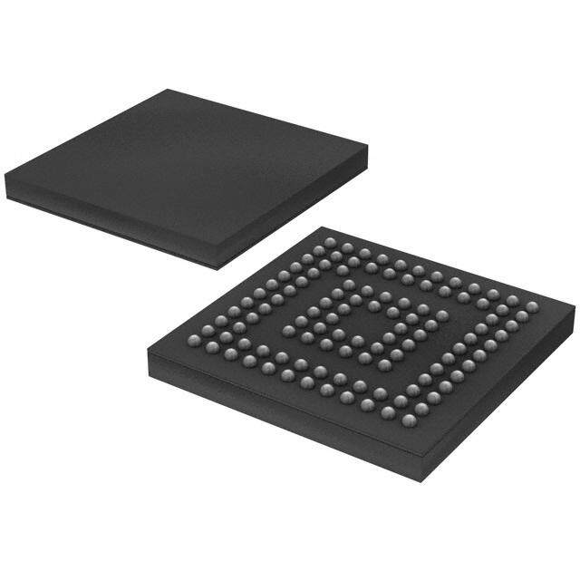
4. Package and Pinout The AT91SAM9R64 is available in a 144-ball BGA package. The AT91SAM9RL64 is available in a 217-ball LFBGA package. 4.1 144-ball BGA Package Outline Figure 4-1 shows the orientation of the 144-ball BGA package. Figure 4-1. 144-ball BGA Pinout (Top View) 12 11 10 9 8 7 6 5 4 3 2 1 A B CDE F GHJ K L M BALL A1 AT91SAM9R64/RL64 12 6289D–ATARM–3-Oct-11
AT91SAM9R64/RL64 4.2 Pinout Table 4-1. AT91SAM9R64 Pinout for 144-ball BGA Package Pin Signal Name Pin Signal Name Pin Signal Name Pin Signal Name A1 DFSDM D1 PLLRCA G1 PB[10] K1 A[5] A2 DHSDM D2 VDDUTMII G2 PB[11] K2 A[6] A3 XIN D3 NWR3/NBS3/CFIOW G3 PB[12] K3 A[13] A4 XOUT D4 NWR1/NBS1/CFIOR G4 PB[9] K4 A[15] A5 XIN32 D5 JTAGSEL G5 PB[13] K5 RAS A6 XOUT32 D6 GNDBU G6 GND K6 D[3] A7 TDO D7 TCK G7 GND K7 D[6] A8 PA[31] D8 PA[26] G8 GND K8 D[13] A9 PA[22] D9 PA[24] G9 GNDUTMI K9 VDDIOM A10 PA[16] D10 PA[13] G10 VDDCORE K10 VDDIOM A11 PA[14] D11 PA[6] G11 VDDIOP K11 D[11] A12 PA[11] D12 PD[20] G12 VDDIOP K12 PB[1] B1 DFSDP E1 GNDPLLA H1 PB[14] L1 A[7] B2 DHSDP E2 NWR0/NWE/CFWE H2 PB[15] L2 A[8] B3 NC E3 NRD/CFOE H3 A[0] L3 A[11] B4 VDDPLLB E4 NCS0 H4 A[2] L4 A[16] B5 GNDPLLB E5 NCS1/SDCS H5 SDA10 L5 SDWE B6 TMS E6 PB[2] H6 D[1] L6 D[4] B7 RTCK E7 NRST H7 GND L7 D[7] B8 PA[27] E8 BMS H8 GND L8 D[15] B9 PA[21] E9 PA[25] H9 VDDIOM L9 PC[1] B10 PA[12] E10 PA[15] H10 SDCKE L10 PC[0] B11 PD[21] E11 PA[5] H11 VDDCORE L11 PB[0] B12 PA[10] E12 PA[4] H12 VDDIOP L12 GNDANA C1 VDDPLLA F1 PB[5] J1 A[4] M1 A[9] C2 VBG F2 PB[6] J2 A[1] M2 A[10] C3 VDDBU F3 PB[7] J3 A[3] M3 A[12] C4 SHDN F4 PB[8] J4 A[14] M4 A[17] C5 WKUP F5 PB[3] J5 CAS M5 D[0] C6 NTRST F6 PB[4] J6 D[2] M6 SDCK C7 TDI F7 TST J7 D[5] M7 D[8] C8 PA[28] F8 VDDUTMIC J8 D[12] M8 ADVREF C9 PA[23] F9 PA[3] J9 D[14] M9 VDDANA C10 PA[7] F10 PA[2] J10 VDDIOM M10 PA[17] C11 PD[19] F11 PA[0] J11 D[10] M11 PA[18] C12 PD[18] F12 PA[1] J12 D[9] M12 PA[19] 13 6289D–ATARM–3-Oct-11
4.3 217-ball LFBGA Package Outline Figure 4-2 shows the orientation of the 217-ball LFBGA package. Figure 4-2. 217-ball LFBGA Pinout (Top View) 17 16 15 14 13 12 11 10 9 8 7 6 5 4 3 2 1 A B CDE F GHJ K L M NP RT U BALL A1 AT91SAM9R64/RL64 14 6289D–ATARM–3-Oct-11
AT91SAM9R64/RL64 4.4 Pinout Table 4-2. AT91SAM9RL64 Pinout for 217-ball LFBGA Package (1) Pin Signal Name Pin Signal Name Pin Signal Name Pin Signal Name A1 DFSDM D5 SHDN J14 PD[1] P17 PC[11] A2 DHSDP D6 JTAGSEL J15 PD[0] R1 A[0] A3 VDDPLLB D7 NTRST J16 PC[30] R2 A[2] A4 XIN D8 BMS J17 PC[31] R3 A[7] A5 XOUT D9 TDO K1 PB[14] R4 A[10] A6 GNDPLLB D10 PA[30] K2 PB[15] R5 A[14] A7 XOUT32 D11 GND K3 PB[17] R6 SDA10 A8 GND D12 PA[23] K4 PB[16] R7 D[0] A9 NRST D13 PA[15] K8 VDDUTMIC R8 VDDIOM A10 RTCK D14 PA[12] K9 VDDIOP R9 D[6] A11 PA[29] D15 PA[8] K10 PC[28] R10 D[9] A12 PA[26] D16 PD[13] K14 PC[25] R11 NC A13 PA[22] D17 PD[16] K15 PC[24] R12 VDDIOM A14 PA[14] E1 GNDPLLA K16 PC[26] R13 PC[1] A15 PA[10] E2 NCS1/SDCS K17 PC[27] R14 PB[1] A16 PD[20] E3 NCS0 L1 PB[18] R15 PC[5] A17 PD[17] E4 NWR3/NBS3/CFIOW L2 PB[19] R16 PC[6] B1 DFSDP E14 PD[15] L3 PB[21] R17 PC[7] B2 DHSDM E15 PD[14] L4 PB[20] T1 A[3] B3 VBG E16 PA[5] L14 PC[21] T2 A[5] B4 NC E17 PA[4] L15 PC[20] T3 A[8] B5 NC F1 NRD/CFOE L16 PC[22] T4 A[12] B6 XIN32 F2 PB[2] L17 PC[23] T5 A[16] B7 TST F3 NWR0/NWE/CFWE M1 PB[22] T6 RAS B8 GND F4 PB[3] M2 PB[23] T7 D[2] B9 TMS F14 PA[1] M3 PB[25] T8 D[4] B10 VDDCORE F15 PA[0] M4 PB[24] T9 D[7] B11 PA[28] F16 PA[2] M14 PC[17] T10 D[10] B12 PA[25] F17 PA[3] M15 PC[16] T11 D[14] B13 PA[21] G1 GND M16 PC[18] T12 VDDANA B14 PA[13] G2 VDDIOM M17 PC[19] T13 PA[17] B15 PD[21] G3 PB[5] N1 PB[26] T14 PA[19] B16 PD[19] G4 PB[4] N2 PB[27] T15 PC[2] B17 PA[9] G14 PD[12] N3 PB[29] T16 PC[3] C1 VDDPLLA G15 PD[11] N4 PB[28] T17 PC[4] C2 VDDUTMII G16 PD[10] N14 PC[13] U1 A[4] C3 GND G17 PD[9] N15 PC[12] U2 A[6] C4 GNDUTMI H1 PB[8] N16 PC[14] U3 A[9] C5 VDDBU H2 PB[9] N17 PC[15] U4 A[13] C6 WKUP H3 PB[7] P1 PB[30] U5 A[17] C7 GNDBU H4 PB[6] P2 PB[31] U6 SDWE C8 TCK H8 VDDCORE P3 A[1] U7 D[3] C9 TDI H9 VDDIOP P4 A[11] U8 SDCK C10 PA[31] H10 PD[4] P5 A[15] U9 D[11] C11 PA[27] H14 PD[8] P6 CAS U10 D[12] C12 PA[24] H15 PD[5] P7 D[1] U11 D[13] C13 PA[16] H16 PD[2] P8 SDCKE U12 TSADVREF C14 PA[11] H17 PD[3] P9 D[5] U13 PA[18] C15 PD[18] J1 PB[12] P10 D[8] U14 PA[20] C16 PA[7] J2 PB[13] P11 D[15] U15 PD[6] C17 PA[6] J3 PB[11] P12 PC[0] U16 PD[7] D1 PLLRCA J4 PB[10] P13 PB[0] U17 GNDANA D2 NWR1/NBS1/CFIOR J8 VDDCORE P14 PC[8] D3 GND J9 VDDIOP P15 PC[9] D4 GND J10 PC[29] P16 PC[10] Note: 1. Shaded cells define the pins powered by VDDIOM. 15 6289D–ATARM–3-Oct-11
5. Power Considerations 5.1 Power Supplies The AT91SAM9R64/RL64 has several types of power supply pins: (cid:129) VDDCORE pins: Power the core, including the processor, the embedded memories and the peripherals; voltage ranges from 1.08V and 1.32V, 1.2V nominal. (cid:129) VDDIOM pins: Power the External Bus Interface; voltage ranges between 1.65V and 1.95V (1.8V nominal) or between 3.0V and 3.6V (3.3V nominal). (cid:129) VDDIOP pins: Power the Peripherals I/O lines; voltage ranges from 3.0V and 3.6V, 3.3V nominal. (cid:129) VDDBU pin: Powers the Slow Clock oscillator and a part of the System Controller; voltage ranges from 1.08V and 1.32V, 1.2V nominal. (cid:129) VDDPLLA pin: Powers the PLL cell; voltage ranges from 3.0V and 3.6V, 3.3V nominal. (cid:129) VDDPLLB pin: Powers the UTMI PLL (480MHz) and OSC 12M cells; voltage ranges from 1.08V and 1.32V, 1.2V nominal. (cid:129) VDDUTMII pin: Powers the UTMI+ interface; voltage ranges from 3.0V and 3.6V, 3.3V nominal. (cid:129) VDDUTMIC pin: Powers the UTMI+ core; voltage ranges from 1.08V and 1.32V, 1.2V nominal. (cid:129) VDDANA pin: Powers the ADC cell; voltage ranges from 3.0V and 3.6V, 3.3V nominal. The power supplies VDDIOM and VDDIOP are identified in the pinout table and the PIO multi- plexing tables. These supplies enable the user to power the device differently for interfacing with memories and for interfacing with peripherals. Ground pins GND are common to VDDCORE, VDDIOM and VDDIOP pins power supplies. Separated ground pins are provided for VDDBU, VDDPLLA, VDDPLLB and VDDANA. These ground pins are respectively GNDBU, GNDPLLA, GNDPLLB and GNDANA. A common ground pin is provided for VDDUTMII and VDDUTMIC. This ground pin is GNDUTMI. Caution: VDDCORE and VDDIO constraints at startup to be checked in the Core Power Supply POR Characteristics in the Electrical Characteristics section of the datasheet. 5.1.1 USB Power Supply Considerations To achieve the best performances on the UDPHS, care must be taken in the power supplies choice and especially on VDDPLLB,VDDUTMIC and VDDUTMII. The USB High speed requires power supplies with a ripple voltage < 20 mV on VDDPLLB and VDDUTMIC. The VDDUTMII powering the UTMI transceiver must also be filtered. It is highly recommended to use an LDO linear regulator to generate the 1.2 volts for both VDDPLLB and VDDUTMIC. VDDUTMII can be connected on the 3.3 volts of the system via an LC filter. The figure below gives an example of VDDPLLB, VDDUTMIC and VDDUTMII. AT91SAM9R64/RL64 16 6289D–ATARM–3-Oct-11
AT91SAM9R64/RL64 Figure 5-1. Example of PLL and USB Power Supplies VIN VIN VOUT 1V2_USB 10µF 0.1µF CE 1K 10µF ADJ VSS 100K MIC5235YM5 2.2µH 1V2_USB VDDPLLB 0.1µF 2.2µH 1V2_USB VDDUTMIC 0.1µF 2.2µH 3V3 VDDUTMII 0.1µF 5.2 Programmable I/O Lines Power Supplies The power supplies pins VDDIOM support two voltage ranges. This allows the device to reach its maximum speed either out of 1.8V or 3.3V external memories. The maximum speed is MCK on the pin SDCK (SDRAM Clock) loaded with 30pF for power sup- ply at 1.8V and 50 pF for power supply at 3.3V. The maximum speed on the other signals of the External Bus Interface (control, address and data signals) is 50 MHz. The voltage ranges are determined by programming registers in the Chip Configuration registers located in the Matrix User Interface. At reset, the selected voltage defaults to 3.3V nominal and power supply pins can accept either 1.8V or 3.3V. The user must make sure to program the EBI voltage range before getting the device out of its Slow Clock Mode. The PIO lines are supplied through VDDIOP and the speed of the signal that can be driven on them can reach 50 MHz with 50 pF load. 17 6289D–ATARM–3-Oct-11
6. I/O Line Considerations 6.1 JTAG Port Pins TMS, TDI and TCK are schmitt trigger inputs and have no pull-up resistors. TDO is an output, driven at up to VDDIOP, and have no pull-up resistor. The JTAGSEL pin is used to select the JTAG boundary scan when asserted at a high level. It integrates a permanent pull-down resistor of about 15 kΩ to GNDBU, so that it can be left uncon- nected for normal operations. All the JTAG signals are supplied with VDDIOP except JTAGSEL supplied by VDDBU. 6.2 Test Pin The TST pin is used for manufacturing test purposes when asserted high. It integrates a perma- nent pull-down resistor of about 15 kΩ to GNDBU, so that it can be left unconnected for normal operations. Driving this line at a high level leads to unpredictable results. This pin is supplied with VDDBU. 6.3 Reset Pins NRST is an open-drain output integrating a non-programmable pull-up resistor. It can be driven with voltage at up to VDDIOP. As the product integrates power-on reset cells, which manages the processor and the JTAG reset, the NRST and NTRST pin can be left unconnected. The NRST and NTRST pins integrates a permanent pull-up resistor of 100 kΩ typical to VDDIOP. The NRST signal is inserted in the Boundary Scan. 6.4 PIO Controllers All the I/O lines which are managed by the PIO Controllers integrate a programmable pull-up resistor. Refer to the section “AT91SAM9R64/RL64 Electrical Characteristics” in the product datasheet for more details. After reset, all the I/O lines default as inputs with pull-up resistors enabled, except those which are multiplexed with the External Bus Interface signals that require to be enabled as Peripheral at reset. This is explicitly indicated in the column “Reset State” of the PIO Controller multiplexing tables. 6.5 Shutdown Logic Pins The pin WKUP is an input-only. It can accept voltages only between 0V and VDDBU. 7. Processor and Architecture 7.1 ARM926EJ-S Processor (cid:129) RISC Processor Based on ARM v5TEJ Architecture with Jazelle technology for Java acceleration (cid:129) Two Instruction Sets AT91SAM9R64/RL64 18 6289D–ATARM–3-Oct-11
AT91SAM9R64/RL64 – ARM High-performance 32-bit Instruction Set – Thumb High Code Density 16-bit Instruction Set (cid:129) DSP Instruction Extensions (cid:129) 5-Stage Pipeline Architecture: – Instruction Fetch (F) – Instruction Decode (D) – Execute (E) – Data Memory (M) – Register Write (W) (cid:129) 4-Kbyte Data Cache, 4-Kbyte Instruction Cache – Virtually-addressed 4-way Associative Cache – Eight words per line – Write-through and Write-back Operation – Pseudo-random or Round-robin Replacement (cid:129) Write Buffer – Main Write Buffer with 16-word Data Buffer and 4-address Buffer – DCache Write-back Buffer with 8-word Entries and a Single Address Entry – Software Control Drain (cid:129) Standard ARM v4 and v5 Memory Management Unit (MMU) – Access Permission for Sections – Access Permission for large pages and small pages can be specified separately for each quarter of the page – 16 embedded domains (cid:129) Bus Interface Unit (BIU) – Arbitrates and Schedules AHB Requests – Separate Masters for both instruction and data access providing complete Matrix system flexibility – Separate Address and Data Buses for both the 32-bit instruction interface and the 32-bit data interface – On Address and Data Buses, data can be 8-bit (Bytes), 16-bit (Half-words) or 32-bit (Words) 7.2 Matrix Masters The Bus Matrix of the AT91SAM9R64/RL64 product manages 6 masters, which means that each master can perform an access concurrently with others, to an available slave. Each master has its own decoder, which is defined specifically for each master. In order to sim- plify the addressing, all the masters have the same decodings. Table 7-1. List of Bus Matrix Masters Master 0 DMA Controller Master 1 USB Device High Speed DMA Master 2 LCD Controller DMA 19 6289D–ATARM–3-Oct-11
Table 7-1. List of Bus Matrix Masters Master 3 Peripheral DMA Controller Master 4 ARM926™ Instruction Master 5 ARM926 Data 7.3 Matrix Slaves The Bus Matrix of the AT91SAM9R64/RL64 product manages 6 slaves. Each slave has its own arbiter, allowing a different arbitration per slave. Table 7-2. List of Bus Matrix Slaves Slave 0 Internal ROM Slave 1 Internal SRAM Slave 2 LCD Controller User Interface Slave 3 UDP High Speed RAM Slave 4 External Bus Interface (EBI) Slave 5 Peripheral Bridge 7.4 Master to Slave Access All the Masters can normally access all the Slaves. However, some paths do not make sense, for example allowing access from the USB Device High speed DMA to the Internal Peripherals. Thus, these paths are forbidden or simply not wired, and shown as “-” in the following table. Table 7-3. AT91SAM9R64/RL64 Master to Slave Access Masters 0 1 2 3 4 5 LCD DMA USB HS Peripheral ARM926 ARM926 Slaves Controller Controller Device DMA DMA Instruction Data DMA 0 Internal ROM X X X X X 1 Internal SRAM X X X X X X 2 LCD Controller User Interface - - - - X X 3 UDP High Speed RAM - - - - X X 4 External Bus Interface X X X X X X 5 Peripheral Bridge X X X - - - 7.5 Peripheral DMA Controller (PDC) (cid:129) Acting as one AHB Bus Matrix Master (cid:129) Allows data transfers from/to peripheral to/from any memory space without any intervention of the processor. (cid:129) Next Pointer support, prevents strong real-time constraints on buffer management. The Peripheral DMA Controller handles transfer requests from the channel according to the fol- lowing priorities (Low to High priorities): AT91SAM9R64/RL64 20 6289D–ATARM–3-Oct-11
AT91SAM9R64/RL64 a. TWI0 Transmit Channel b. DBGU Transmit Channel c. USART3 Transmit Channel d. USART2 Transmit Channel e. USART1 Transmit Channel f. USART0 Transmit Channel g. AC97 Transmit Channel h. SPI Transmit Channel i. SSC1 Transmit Channel j. SSC0 Transmit Channel k. TWI0 Receive Channel l. DBGU Receive Channel m. ADC Receive Channel n. USART3 Receive Channel o. USART2 Receive Channel p. USART1 Receive Channel q. USART0 Receive Channel r. AC97 Receive Channel s. SPI Receive Channel t. SSC1 Receive Channel u. SSC0 Transmit Channel v. MCI Receive/Transmit Channel 7.6 DMA Controller (cid:129) Acting as one Matrix Master (cid:129) Embeds 2 channels (cid:129) 16 bytes/FIFO for Channel Buffering (cid:129) Linked List support with Status Write Back operation at End of Transfer (cid:129) Word, Half-word, Byte transfer support 7.7 Debug and Test Features (cid:129) ARM926 Real-time In-circuit Emulator – Two real-time Watchpoint Units – Two Independent Registers: Debug Control Register and Debug Status Register – Test Access Port Accessible through JTAG Protocol – Debug Communications Channel (cid:129) Debug Unit – Two-pin UART – Debug Communication Channel Interrupt Handling – Chip ID Register (cid:129) IEEE1149.1 JTAG Boundary-scan on All Digital Pins 21 6289D–ATARM–3-Oct-11
8. Memories Figure 8-1. AT91SAM9R64/RL64 Memory Mapping Address Memory Space Internal Memory Mapping 0x0000 0000 0x0000 0000 Notes : Boot Memory (1) 1 MBytes (1) Can be SRAM, ROM depending Internal Memories 256M Bytes 0x0010 0000 on BMS and the REMAP Command 0x0FFF FFFF ITCM(2) 1 MBytes (2) Software programmable 0x1000 0000 0x0020 0000 EBI DTCM(2) 1 MBytes Chip Select 0 256M Bytes 0x0030 0000 0x02x010FF0F 0 F0F0F0F SRAM(2) 1 MBytes EBI 0x0040 0000 Chip Select 1/ 256M Bytes ROM 1 MBytes SDRAMC 0x2FFF FFFF 0x0050 0000 0x3000 0000 LCD Controller User Interface 1 MBytes EBI Chip Select 2 256M Bytes 0x0060 0000 UDPHS RAM 1 MBytes 0x3FFF FFFF 0x4000 0000 0x0070 0000 EBI Chip Select 3/ 256M Bytes Undefined NANDFlash (Abort) 0x4FFF FFFF 0x5000 0000 EBI 0x0FFF FFFF System Controller Mapping Chip Select 4/ 256M Bytes Compact Flash 0xFFFF C000 0x5FFF FFFF Slot 0 Peripheral Mapping 0x6000 0000 EBI 0xF000 0000 Reserved Chip Select 5/ 256M Bytes Reserved Compact Flash 0xFFFF E600 0x6FFF FFFF Slot 1 0xFFFA 0000 DMAC 512 Bytes 0x7000 0000 TCO, TC1, TC2 16K Bytes 0xFFFF E800 0xFFFA 4000 ECC 512 Bytes MCI 16K Bytes 0xFFFF EA00 0xFFFA 8000 SDRAMC 512 Bytes TWI0 16K Bytes 0xFFFF EC00 0xFFFA C000 SMC 512 bytes TWI1 16K Bytes 0xFFFF EE00 0xFFFB 0000 0xFFFF EF10 MATRIX 512 Bytes USART0 16K Bytes 0xFFFF F000 0xFFFB 4000 AIC 512 Bytes USART1 16K Bytes 0xFFFF F200 0xFFFB 8000 DBGU 512 Bytes USART2 16K Bytes 0xFFFF F400 Undefined 0xFFFB C000 PIOA 512 Bytes (Abort) UART3 16K Bytes 0xFFFF F600 0xFFFC 0000 PIOB 512 Bytes SSC0 16K Bytes 0xFFFF F800 0xFFFC 4000 PIOC 512 bytes 2,048M Bytes SSC1 16K Bytes 0xFFFF FA00 0xFFFC 8000 PIOD 512 bytes PWMC 16K Bytes 0xFFFF FC00 0xFFFC C000 PMC 256 Bytes SPI 16K Bytes 0xFFFF FD00 0xFFFD 0000 RSTC 16 Bytes ToucAhDSCcreen 16K Bytes 0xFFFF FD10 SHDC 16 Bytes 0xFFFF FD20 0xFFFD 4000 RTTC 16 Bytes UDPHS 16K Bytes 0xFFFF FD30 PITC 16 Bytes 0xFFFD 8000 0xFFFF FD40 WDTC 16 Bytes AC97 16K Bytes 0xFFFF FD50 SCKCR 16 Bytes 0xFFFD C000 0xFFFF FD60 0xEFFF FFFF GPBR 16 Bytes 0xF000 0000 Reserved 0xFFFF FD70 Reserved 0xFFFF C000 0xFFFF FE00 Internal Peripherals 256M Bytes RTCC 128 Bytes SYSC 16K Bytes 0xFFFF FFFF 0xFFFF FFFF 0xFFFF FFFF Reserved AT91SAM9R64/RL64 22 6289D–ATARM–3-Oct-11
AT91SAM9R64/RL64 A first level of address decoding is performed by the AHB Bus Matrix, i.e., the implementation of the Advanced High performance Bus (AHB) for its Master and Slave interfaces with additional features. Decoding breaks up the 4G bytes of address space into 16 banks of 256M bytes. The banks 1 to 8 are directed to the EBI that associates these banks to the external chip selects EBI_NCS0 to EBI_NCS5. The bank 0 is reserved for the addressing of the internal memories, and a second level of decoding provides 1M byte of internal memory area. The bank 15 is reserved for the peripherals and provides access to the Advanced Peripheral Bus (APB). Other areas are unused and performing an access within them provides an abort to the master requesting such an access. 8.1 Embedded Memories (cid:129) 32 KB ROM – Single Cycle Access at full bus speed (cid:129) 64 KB Fast SRAM – Single Cycle Access at full bus speed – Supports ARM926EJ-S TCM interface at full processor speed 8.1.1 Internal Memory Mapping Table 8-1 summarizes the Internal Memory Mapping for each Master, depending on the Remap status (RCBx bit) and the BMS state at reset. Table 8-1. Internal Memory Mapping RCBx(1) = 0 RCBx(1) = 1 Address BMS = 1 BMS =0 0x0000 0000 ROM EBI_NCS0(2) SRAM Notes: 1. x = 0 to maximum Master number. 2. EBI NCS0 is to be connected to a 16-bit non-volatile memory. The access configuration is defined by the reset state of SMC Setup, SMC Pulse, SMC Cycle and SMC Mode CS0 registers. 8.1.1.1 Internal SRAM The AT91SAM9R64/RL64 product embeds a total of 64Kbyte high-speed SRAM split in 4 blocks of 16KBytes. After reset and until the Remap Command is performed, the SRAM is only accessible at address 0x0030 0000. After Remap, the SRAM also becomes available at address 0x0. This Internal SRAM can be allocated to threes areas. Its Memory Mapping is detailed in Table 8- 2. (cid:129) Internal SRAM A is the ARM926EJ-S Instruction TCM. The user can map this SRAM block anywhere in the ARM926 instruction memory space using CP15 instructions and the TCR configuration register located in the Chip Configuration User Interface. This SRAM block is also accessible by the ARM926 Data Master and by the AHB Masters through the AHB bus at address 0x0010 0000. 23 6289D–ATARM–3-Oct-11
(cid:129) Internal SRAM B is the ARM926EJ-S Data TCM. The user can map this SRAM block anywhere in the ARM926 data memory space using CP15 instructions. This SRAM block is also accessible by the ARM926 Data Master and by the AHB Masters through the AHB bus at address 0x0020 0000. (cid:129) Internal SRAM C is only accessible by all the AHB Masters. After reset and until the Remap Command is performed, this SRAM block is accessible through the AHB bus at address 0x0030 0000 by all the AHB Masters. After Remap, this SRAM block also becomes accessible through the AHB bus at address 0x0 by the ARM926 Instruction and the ARM926 Data Masters. Within the 64Kbyte SRAM size available, the amount of memory assigned to each block is soft- ware programmable as a multiple of 16K Bytes according to Table 8-2. This Table provides the size of the Internal SRAM C according to the size of the Internal SRAM A and the Internal SRAM B. Table 8-2. Internal SRAM Block Size Internal SRAM A (ITCM) Size Remaining Internal SRAM C 0 16K Bytes 32K Bytes 0 64K Bytes 48K Bytes 32K Bytes Internal SRAM B (DTCM) size 16K Bytes 48K Bytes 32K Bytes 16K Bytes 32K Bytes 32K Bytes 16K Bytes 0K Bytes At reset, the whole memory is assigned to Internal SRAM C. The memory blocks assigned to SRAM A, SRAM B and SRAM C areas are not contiguous and when the user dynamically changes the Internal SRAM configuration, the new 16-Kbyte block organization may affect the previous configuration from a software point of view. Table 8-3 illustrates different configurations and the related 16-Kbyte blocks (RB0 to RB3) assignments. Table 8-3. 16-Kbyte Block Allocation example Configuration examples and related 16-Kbyte block assignments Decoded I = 0K I = 16K I =32K I = 0K I = 16K I = 32K I = 0K I = 16K I = 32K Address Area D = 0K D = 0K D = 0K D = 16K D = 16K D = 16K D = 32K D = 32K D = 32K A = 64K(1) A = 48K A = 32K A = 48K A = 32K A = 16K A = 32K A = 16K A = 0K Internal 0x0010 0000 RB1 RB1 RB1 RB1 RB1 RB1 SRAM A (ITCM) 0x0010 4000 RB0 RB0 RB0 Internal 0x0020 0000 RB3 RB3 RB3 RB3 RB3 RB3 SRAM B (DTCM) 0x0020 4000 RB2 RB2 RB2 0x0030 0000 RB3 RB3 RB3 RB2 RB2 RB2 RB1 RB0 Internal 0x0030 4000 RB2 RB2 RB2 RB1 RB0 RB0 SRAM C (AHB) 0x0030 8000 RB1 RB0 RB0 0x0030 C000 RB0 Note: 1. Configuration after reset. AT91SAM9R64/RL64 24 6289D–ATARM–3-Oct-11
AT91SAM9R64/RL64 When accessed from the AHB, the internal Fast SRAM is single cycle accessible at full matrix speed (MCK). When accessed from the processor’s TCM Interface, they are also single cycle accessible at full processor speed. 8.1.1.2 Internal ROM The AT91SAM9R64/RL64 embeds an Internal ROM, which contains the SAM-BA program. At any time, the ROM is mapped at address 0x0040 0000. It is also accessible at address 0x0 (BMS =1) after the reset and before the Remap Command. 8.1.2 Boot Strategies The system always boots at address 0x0. To ensure maximum boot possibilities, the memory layout can be changed with two parameters. REMAP allows the user to layout the internal SRAM bank to 0x0 to ease the development. This is done by software once the system has boot. Refer to the Bus Matrix Section for more details. When REMAP = 0 BMS allows the user to lay out to 0x0, at his convenience, the ROM or an external memory. This is done by a hardware way at reset. Note: All the memory blocks can always be seen at their specified base addresses that are not concerned by these parameters. The AT91SAM9R64/RL64 Bus Matrix manages a boot memory that depends on the level on the pin BMS at reset. The internal memory area mapped between address 0x0 and 0x000F FFFF is reserved to this effect. If BMS is detected at 1, the boot memory is the embedded ROM. If BMS is detected at 0, the boot memory is the memory connected on the Chip Select 0 of the External Bus Interface. 8.1.2.1 BMS = 1, boot on embedded ROM The system boots on Boot Program. (cid:129) Boot on on-chip RC (cid:129) Enable the 32768 Hz oscillator (cid:129) Auto baudrate detection (cid:129) Downloads and runs an application from external storage media into internal SRAM (cid:129) Downloaded code size depends on embedded SRAM size (cid:129) Automatic detection of valid application (cid:129) Bootloader on a non-volatile memory – SDCard (boot ROM does not support high-capacity SDCards) – NAND Flash – SPI DataFlash® connected on NPCS0 of the SPI0 (cid:129) SAM-BA Boot in case no valid program is detected in external NVM, supporting – Serial communication on a DBGU – USB Device HS Port 8.1.2.2 BMS = 0, boot on external memory (cid:129) Boot on on-chip RC 25 6289D–ATARM–3-Oct-11
(cid:129) Boot with the default configuration for the Static Memory Controller, byte select mode, 16-bit data bus, Read/Write controlled by Chip Select, allows boot on 16-bit non-volatile memory. For optimization purposes, nothing else is done. To speed up the boot sequence user pro- grammed software should perform a complete configuration: (cid:129) Enable the 32768 Hz oscillator if best accuracy needed (cid:129) Program the PMC (main oscillator enable or bypass mode) (cid:129) Program and Start the PLL (cid:129) Reprogram the SMC setup, cycle, hold, mode timings registers for CS0 to adapt them to the new clock (cid:129) Switch the main clock to the new value 8.2 External Memories The AT91SAM9R64/RL64 features one External Bus Interface to offer interface to a wide range of external memories and to any parallel peripheral. 8.2.1 External Bus Interface (cid:129) Integrates three External Memory Controllers: – Static Memory Controller – SDRAM Controller – SLC Nand Flash ECC Controller (cid:129) Additional logic for NAND Flash and CompactFlashTM (cid:129) Optional Full 32-bit External Data Bus (cid:129) Up to 26-bit Address Bus (up to 64MBytes linear per chip select) (cid:129) Up to 6 chips selects, Configurable Assignment: – Static Memory Controller on NCS0 – SDRAM Controller (SDCS) or Static Memory Controller on NCS1 – Static Memory Controller on NCS2 – Static Memory Controller on NCS3, Optional NAND Flash support – Static Memory Controller on NCS4 - NCS5, Optional CompactFlashM support 8.2.2 Static Memory Controller (cid:129) 8-, 16- or 32-bit Data Bus (cid:129) Multiple Access Modes supported – Byte Write or Byte Select Lines – Asynchronous read in Page Mode supported (4- up to 32-byte page size) (cid:129) Multiple device adaptability – Control signals programmable setup, pulse and hold time for each Memory Bank (cid:129) Multiple Wait State Management – Programmable Wait State Generation – External Wait Request – Programmable Data Float Time (cid:129) Slow Clock mode supported AT91SAM9R64/RL64 26 6289D–ATARM–3-Oct-11
AT91SAM9R64/RL64 8.2.3 SDRAM Controller (cid:129) Supported devices: – Standard and Low Power SDRAM (Mobile SDRAM) – 2K, 4K, 8K Row Address Memory Parts – SDRAM with two or four Internal Banks – SDRAM with 16- or 32-bit Data Path (cid:129) Programming facilities – Word, half-word, byte access – Automatic page break when Memory Boundary has been reached – Multibank Ping-pong Access – Timing parameters specified by software – Automatic refresh operation, refresh rate is programmable (cid:129) Energy-saving capabilities – Self-refresh, power down and deep power down modes supported (cid:129) Error detection – Refresh Error Interrupt (cid:129) SDRAM Power-up Initialization by software (cid:129) SDRAM CAS Latency of 1, 2 and 3 supported (cid:129) Auto Precharge Command not used 8.2.4 NAND Flash Error Corrected Code Controller (cid:129) Tracking the accesses to a NAND Flash device by trigging on the corresponding chip select (cid:129) Single bit error correction and 2-bit Random detection. (cid:129) Automatic Hamming Code Calculation while writing – ECC value available in a register (cid:129) Automatic Hamming Code Calculation while reading – Error Report, including error flag, correctable error flag and word address being detected erroneous – Support 8- or 16-bit NAND Flash devices with 512-, 1024-, 2048- or 4096-bytes pages 27 6289D–ATARM–3-Oct-11
9. System Controller The System Controller is a set of peripherals, which allow handling of key elements of the sys- tem, such as power, resets, clocks, time, interrupts, watchdog, etc. The System Controller User Interface embeds also the registers allowing to configure the Matrix and a set of registers configuring the EBI chip select assignment and the voltage range for exter- nal memories. 9.1 System Controller Mapping As shown in Figure 8-1, the System Controller’s peripherals are all mapped within the highest 16K bytes of the 4 Gbyte address space, between addresses 0xFFFF C000 and 0xFFFF FFFF. However, all the registers of System Controller are mapped on the top of the address space. This allows addressing all the registers of the System Controller from a single pointer by using the standard ARM instruction set, as the Load/Store instruction have an indexing mode of +/- 4kbytes. AT91SAM9R64/RL64 28 6289D–ATARM–3-Oct-11
AT91SAM9R64/RL64 9.2 Block Diagram Figure 9-1. System Controller Block Diagram System Controller VDDCORE Powered irq0-irq2 nirq fiq Advanced nfiq Interrupt periph_irq[2..24] Controller pit_irq int rtt_irq wdt_irq ntrst dbgu_irq por_ntrst ARM926EJ-S pmc_irq rstc_irq periph_nrMeCseKt Debug dbgu_irq proc_nreset Unit dbgu_txd PCK dbgu_rxd debug MCK Periodic debug Interval pit_irq periph_nreset Timer SLCK jtag_nreset Boundary Scan debidulge WaTticmhedrog wdt_irq TAP Controller proc_nreset MCK wdt_fault WDRPROC periph_nreset Bus Matrix NRST rtt_alarm rstc_irq VDDCORE pjtoarg__nntrrsetset periph_nreset POR Reset proc_nreset Controller backup_nreset VDDBU VDDBU VDDBU Powered POR SLCK SLCK Real-Time rtc_irq backup_nreset Clock rtc_alarm SLCK Real-Time rtt_irq backup_nreset Timer rtt_alarm HSCK SLCK SHDN periph_clk[22] USB High Speed WKUP backup_nreset Shutdown periph_nreset DePvoircte rtc_alarm Controller periph_irq[22] RC rtt_alarm OSC 4 General-purpose Backup Registers XIN32 SLOW CLOCK XOUT32 OSC SCKCR SLCK periph_clk[2..24] int pck[0-1] XIN 12MHz MAINCK XOUT MAIN OSC PCK Power UPLL Management MCK Controller HSCK pmc_irq PLLRCA PLLA PLLACK idle periph_clk[6..24] periph_nreset periph_nreset periph_nreset periph_irq[2..4] Embedded periph_clk[2..4] irq Peripherals dbgu_rxd PIO fiq periph_irq[6..24] PA0-PA31 Controllers dbgu_txd PB0-PB31 in PC0-PC31 out PD0-PD21 enable 29 6289D–ATARM–3-Oct-11
9.3 Reset Controller The Reset Controller is based on two Power-on-Reset cells, one on VDDBU and one on VDDCORE. The Reset Controller is capable to return to the software the source of the last reset, either a general reset (VDDBU rising), a wake-up reset (VDDCORE rising), a software reset, a user reset or a watchdog reset. The Reset Controller controls the internal resets of the system and the NRST pin output. It is capable to shape a reset signal for the external devices, simplifying to a minimum connection of a push-button on the NRST pin to implement a manual reset. The configuration of the Reset Controller is saved as supplied on VDDBU. 9.4 Shutdown Controller The Shutdown Controller is supplied on VDDBU and allows a software-controllable shut down of the system through the pin SHDN. An input change of the WKUP pin or an alarm releases the SHDN pin, and thus wakes up the system power supply. 9.5 Clock Generator The Clock Generator is made up of: (cid:129) One low-power 32768 Hz Slow Clock Oscillator with bypass mode (cid:129) One low-power RC oscillator (cid:129) One 12 MHz Main Oscillator, which can be bypassed (cid:129) One 480 MHz PLL (UPLL or PLLB) providing a clock for the USB High Speed Device Controller (cid:129) One 80 to 240 MHz programmable PLL, providing the PLL Clock (PLLCK). This PLL has an input divider to offer a wider range of output frequencies from the 12 MHz input, the only limitation being the lowest input frequency shall be higher or equal to 1 MHz. AT91SAM9R64/RL64 30 6289D–ATARM–3-Oct-11
AT91SAM9R64/RL64 Figure 9-2. Clock Generator Block Diagram Clock Generator RCEN On Chip RC OSC Slow Clock SLCK XIN32 Slow Clock Oscillator XOUT32 OSCSEL OSC32EN OSC32BYP XIN 12M Main Main Clock Oscillator MAINCK XOUT UPLL HSCK (PLLB) PLL and PLL Clock PLLRCA Divider PLLCK Status Control Power Management Controller 9.6 Slow Clock Selection 9.6.1 Description The AT91SAM9R64/RL64 slow clock can be generated either by an external 32768Hz crystal or the on-chip RC oscillator. The 32768Hz crystal oscillator can be bypassed to accept an external slow clock on XIN32. Configuration is located in the slow clock control register (SCKCR) located at address 0xFFFFFD50 in the backed up part of the system controller and so is preserved while VDDBU is present. Refer to the “Clock Generator” section for more details. 9.7 Power Management Controller The Power Management Controller provides all the clock signals to the system. It provides: (cid:129) the Processor Clock PCK (cid:129) the Master Clock MCK, in particular to the Matrix and the memory interfaces (cid:129) the USB Device HS Clock HSCK (cid:129) independent peripheral clocks, typically at the frequency of MCK (cid:129) two programmable clock outputs: PCK0 and PCK1 This allows the software control of five flexible operating modes: (cid:129) Normal Mode, processor and peripherals running at a programmable frequency (cid:129) Idle Mode, processor stopped waiting for an interrupt (cid:129) Slow Clock Mode, processor and peripherals running at low frequency 31 6289D–ATARM–3-Oct-11
(cid:129) Standby Mode, mix of Idle and Backup Mode, peripheral running at low frequency, processor stopped waiting for an interrupt (cid:129) Backup Mode, Main Power Supplies off, VDDBU powered by a battery Figure 9-3. AT91SAM9R64/RL64 Power Management Controller Block Diagram Processor Clock PCK Controller int Master Clock Controller Idle Mode SLCK Prescaler MAINCK MCK /1,/2,/4,...,/64 PLLCK Peripherals Clock Controller periph_clk[..] ON/OFF Programmable Clock Controller ON/OFF SLCK Prescaler MAINCK pck[..] /1,/2,/4,...,/64 PLLCK 9.8 Periodic Interval Timer (cid:129) Includes a 20-bit Periodic Counter, with less than 1 µs accuracy (cid:129) Includes a 12-bit Interval Overlay Counter (cid:129) Real Time OS or Linux®/WindowsCE® compliant tick generator 9.9 Watchdog Timer (cid:129) 16-bit key-protected only-once-Programmable Counter (cid:129) Windowed, prevents the processor to be in a dead-lock on the watchdog access 9.10 Real-Time Timer (cid:129) Real-Time Timer, allowing backup of time with different accuracies – 32-bit Free-running back-up Counter – Integrates a 16-bit programmable prescaler running on slow clock – Alarm Register capable to generate a wake-up of the system through the Shut Down Controller 9.11 Real-Time Clock (cid:129) Low power consumption (cid:129) Full asynchronous design AT91SAM9R64/RL64 32 6289D–ATARM–3-Oct-11
AT91SAM9R64/RL64 (cid:129) Two hundred year calendar (cid:129) Programmable Periodic Interrupt (cid:129) Alarm and update parallel load (cid:129) Control of alarm and update Time/Calendar Data In 9.12 General-Purpose Backed-up Registers (cid:129) Four 32-bit backup general-purpose registers 9.13 Advanced Interrupt Controller (cid:129) Controls the interrupt lines (nIRQ and nFIQ) of the ARM Processor (cid:129) Thirty-two individually maskable and vectored interrupt sources – Source 0 is reserved for the Fast Interrupt Input (FIQ) – Source 1 is reserved for system peripherals (PIT, RTT, PMC, DBGU, etc.) – Programmable Edge-triggered or Level-sensitive Internal Sources – Programmable Positive/Negative Edge-triggered or High/Low Level-sensitive (cid:129) One External Sources plus the Fast Interrupt signal (cid:129) 8-level Priority Controller – Drives the Normal Interrupt of the processor – Handles priority of the interrupt sources 1 to 31 – Higher priority interrupts can be served during service of lower priority interrupt (cid:129) Vectoring – Optimizes Interrupt Service Routine Branch and Execution – One 32-bit Vector Register per interrupt source – Interrupt Vector Register reads the corresponding current Interrupt Vector (cid:129) Protect Mode – Easy debugging by preventing automatic operations when protect modeIs are enabled (cid:129) Fast Forcing – Permits redirecting any normal interrupt source on the Fast Interrupt of the processor 9.14 Debug Unit (cid:129) Composed of two functions – Two-pin UART – Debug Communication Channel (DCC) support (cid:129) Two-pin UART – Implemented features are 100% compatible with the standard Atmel USART – Independent receiver and transmitter with a common programmable Baud Rate Generator – Even, Odd, Mark or Space Parity Generation – Parity, Framing and Overrun Error Detection – Automatic Echo, Local Loopback and Remote Loopback Channel Modes 33 6289D–ATARM–3-Oct-11
– Support for two PDC channels with connection to receiver and transmitter (cid:129) Debug Communication Channel Support – Offers visibility of and interrupt trigger from COMMRX and COMMTX signals from the ARM Processor’s ICE Interface 9.15 Chip Identification (cid:129) Chip ID: 0x019B03A0 (cid:129) JTAG ID: 0x05B2003F (cid:129) ARM926 TAP ID: 0x0792603F 9.16 PIO Controllers (cid:129) 4 PIO Controllers, PIOA, PIOB, PIOC and PIOD, controlling a maximum of 118 I/O Lines (cid:129) Each PIO Controller controls up to 32 programmable I/O Lines – PIOA has 32 I/O Lines – PIOB has 32 I/O Lines – PIOC has 32 I/O Lines – PIOD has 22 I/O Lines (cid:129) Fully programmable through Set/Clear Registers (cid:129) Multiplexing of two peripheral functions per I/O Line (cid:129) For each I/O Line (whether assigned to a peripheral or used as general purpose I/O) – Input change interrupt – Glitch filter – Multi-drive option enables driving in open drain – Programmable pull up on each I/O line – Pin data status register, supplies visibility of the level on the pin at any time (cid:129) Synchronous output, provides Set and Clear of several I/O lines in a single write 10. Peripherals 10.1 Peripheral Mapping As shown in Figure 8-1, the Peripherals are mapped in the upper 256M bytes of the address space between the addresses 0xFFFA 0000 and 0xFFFC FFFF. Each User Peripheral is allocated 16K bytes of address space. AT91SAM9R64/RL64 34 6289D–ATARM–3-Oct-11
AT91SAM9R64/RL64 10.2 Peripheral Identifiers The Table 10-1 defines the Peripheral Identifiers of the AT91SAM9R64/RL64. A peripheral iden- tifier is required for the control of the peripheral interrupt with the Advanced Interrupt Controller and for the control of the peripheral clock with the Power Management Controller. Table 10-1. AT91SAM9R64/RL64 Peripheral Identifiers Peripheral ID Peripheral Mnemonic Peripheral Name External Interrupt 0 AIC Advanced Interrupt Controller FIQ 1 SYSC System Controller Interrupt 2 PIOA Parallel I/O Controller A, 3 PIOB Parallel I/O Controller B 4 PIOC Parallel I/O Controller C 5 PIOD Parallel I/O Controller D 6 US0 USART 0 7 US1 USART 1 8 US2 USART 2 9 US3 USART 3 10 MCI Multimedia Card Interface 11 TWI0 Two-Wire Interface 0 12 TWI1 Two-Wire Interface 1 13 SPI Serial Peripheral Interface 14 SSC0 Synchronous Serial Controller 0 15 SSC1 Synchronous Serial Controller 1 16 TC0 Timer Counter 0 17 TC1 Timer Counter 1 18 TC2 Timer Counter 2 19 PWMC Pulse Width Modulation Controller 20 TSADCC Touch Screen ADC Controller 21 DMAC DMA Controller 22 UDPHS USB Device High Speed 23 LCDC LCD Controller (AT91SAM9RL64 only) 24 AC97 AC97 Controller 25-30 - Reserved 31 AIC Advanced Interrupt Controller IRQ Note: Setting AIC, SYSIRQ, LCDC and IRQ bits in the clock set/clear registers of the PMC has no effect. 35 6289D–ATARM–3-Oct-11
10.3 Peripheral Interrupts and Clock Control 10.3.1 System Interrupt The System Interrupt in Source 1 is the wired-OR of the interrupt signals coming from: (cid:129) the SDRAM Controller (cid:129) the Debug Unit (cid:129) the Periodic Interval Timer (cid:129) the Real-time Timer (cid:129) the Real-time Clock (cid:129) the Watchdog Timer (cid:129) the Reset Controller (cid:129) the Power Management Controller The clock of these peripherals cannot be deactivated and Peripheral ID 1 can only be used within the Advanced Interrupt Controller. 10.3.2 External Interrupts All external interrupt signals, i.e., the Fast Interrupt signal FIQ or the Interrupt signal IRQ, use a dedicated Peripheral ID. However, there is no clock control associated with these peripheral IDs. 10.4 Peripherals Signals Multiplexing on I/O Lines The AT91SAM9R64/RL64 features 4 PIO controllers, PIOA, PIOB, PIOC and PIOD, which mul- tiplexes the I/O lines of the peripheral set. Each PIO Controller controls up to 32 lines. Each line can be assigned to one of two peripheral functions, A or B. The multiplexing tables in the following paragraphs define how the I/O lines of the peripherals A and B are multiplexed on the PIO Controllers. The two columns “Function” and “Comments” have been inserted in this table for the user’s own comments; they may be used to track how pins are defined in an application. Note that some peripheral functions which are output only, might be duplicated within the both tables. The column “Reset State” indicates whether the PIO Line resets in I/O mode or in peripheral mode. If I/O is mentioned, the PIO Line resets in input with the pull-up enabled, so that the device is maintained in a static state as soon as the reset is released. As a result, the bit corre- sponding to the PIO Line in the register PIO_PSR (Peripheral Status Register) resets low. If a signal name is mentioned in the “Reset State” column, the PIO Line is assigned to this func- tion and the corresponding bit in PIO_PSR resets high. This is the case for pins controlling memories, in particular the address lines, which require the pin to be driven as soon as the reset is released. Note that the pull-up resistor is also enabled in this case. The AT91SAM9RL64 and AT91SAM9R64 do not have the same peripheral signal multiplexing, each one follows. AT91SAM9R64/RL64 36 6289D–ATARM–3-Oct-11
AT91SAM9R64/RL64 10.4.1 AT91SAM9RL64 PIO Multiplexing 10.4.1.1 AT91SAM9RL64 PIO Controller A Multiplexing Table 10-2. AT91SAM9RL64 Multiplexing on PIO Controller A PIO Controller A Application Usage Reset Power I/O Line Peripheral A Peripheral B State Supply Function Comments PA0 MC_DA0 I/O VDDIOP PA1 MC_CDA I/O VDDIOP PA2 MC_CK I/O VDDIOP PA3 MC_DA1 TCLK0 I/O VDDIOP PA4 MC_DA2 TIOA0 I/O VDDIOP PA5 MC_DA3 TIOB0 I/O VDDIOP PA6 TXD0 I/O VDDIOP PA7 RXD0 I/O VDDIOP PA8 SCK0 RF1 I/O VDDIOP PA9 RTS0 RK1 I/O VDDIOP PA10 CTS0 RK0 I/O VDDIOP PA11 TXD1 I/O VDDIOP PA12 RXD1 I/O VDDIOP PA13 TXD2 TD1 I/O VDDIOP PA14 RXD2 RD1 I/O VDDIOP PA15 TD0 I/O VDDIOP PA16 RD0 I/O VDDIOP PA17 AD0 I/O VDDANA PA18 AD1 RTS1 I/O VDDANA PA19 AD2 CTS1 I/O VDDANA PA20 AD3 SCK3 I/O VDDANA PA21 DRXD I/O VDDIOP PA22 DTXD RF0 I/O VDDIOP PA23 TWD0 I/O VDDIOP PA24 TWCK0 I/O VDDIOP PA25 MISO I/O VDDIOP PA26 MOSI I/O VDDIOP PA27 SPCK I/O VDDIOP PA28 NPCS0 I/O VDDIOP PA29 RTS2 TF1 I/O VDDIOP PA30 CTS2 TK1 I/O VDDIOP PA31 NWAIT IRQ I/O VDDIOP 37 6289D–ATARM–3-Oct-11
10.4.1.2 AT91SAM9RL64 PIO Controller B Multiplexing Table 10-3. AT91SAM9RL64 Multiplexing on PIO Controller B PIO Controller B Application Usage Reset Power I/O Line Peripheral A Peripheral B State Supply Function Comments PB0 TXD3 I/O VDDIOP PB1 RXD3 I/O VDDIOP PB2 A21/NANDALE A21 VDDIOM PB3 A22/NANDCLE A22 VDDIOM PB4 NANDOE I/O VDDIOM PB5 NANDWE I/O VDDIOM PB6 NCS3/NANDCS I/O VDDIOM PB7 NCS4/CFCS0 NPCS1 I/O VDDIOM PB8 CFCE1 PWM0 I/O VDDIOM PB9 CFCE2 PWM1 I/O VDDIOM PB10 A25/CFRNW FIQ A25 VDDIOM PB11 A18 A18 VDDIOM PB12 A19 A19 VDDIOM PB13 A20 A20 VDDIOM PB14 A23 PCK0 A23 VDDIOM PB15 A24 ADTRG A24 VDDIOM PB16 D16 I/O VDDIOM PB17 D17 I/O VDDIOM PB18 D18 I/O VDDIOM PB19 D19 I/O VDDIOM PB20 D20 I/O VDDIOM PB21 D21 I/O VDDIOM PB22 D22 I/O VDDIOM PB23 D23 I/O VDDIOM PB24 D24 I/O VDDIOM PB25 D25 I/O VDDIOM PB26 D26 I/O VDDIOM PB27 D27 I/O VDDIOM PB28 D28 I/O VDDIOM PB29 D29 I/O VDDIOM PB30 D30 I/O VDDIOM PB31 D31 I/O VDDIOM AT91SAM9R64/RL64 38 6289D–ATARM–3-Oct-11
AT91SAM9R64/RL64 10.4.1.3 AT91SAM9RL64 PIO Controller C Multiplexing Table 10-4. AT91SAM9RL64 Multiplexing on PIO Controller C PIO Controller C Application Usage Reset Power I/O Line Peripheral A Peripheral B State Supply Function Comments PC0 TF0 I/O VDDIOP PC1 TK0 LCDPWR I/O VDDIOP PC2 LCDMOD PWM0 I/O VDDIOP PC3 LCDCC PWM1 I/O VDDIOP PC4 LCDVSYNC I/O VDDIOP PC5 LCDHSYNC I/O VDDIOP PC6 LCDDOTCK I/O VDDIOP PC7 LCDDEN I/O VDDIOP PC8 LCDD0 LCDD2 I/O VDDIOP PC9 LCDD1 LCDD3 I/O VDDIOP PC10 LCDD2 LCDD4 I/O VDDIOP PC11 LCDD3 LCDD5 I/O VDDIOP PC12 LCDD4 LCDD6 I/O VDDIOP PC13 LCDD5 LCDD7 I/O VDDIOP PC14 LCDD6 LCDD10 I/O VDDIOP PC15 LCDD7 LCDD11 I/O VDDIOP PC16 LCDD8 LCDD12 I/O VDDIOP PC17 LCDD9 LCDD13 I/O VDDIOP PC18 LCDD10 LCDD14 I/O VDDIOP PC19 LCDD11 LCDD15 I/O VDDIOP PC20 LCDD12 LCDD18 I/O VDDIOP PC21 LCDD13 LCDD19 I/O VDDIOP PC22 LCDD14 LCDD20 I/O VDDIOP PC23 LCDD15 LCDD21 I/O VDDIOP PC24 LCDD16 LCDD22 I/O VDDIOP PC25 LCDD17 LCDD23 I/O VDDIOP PC26 LCDD18 I/O VDDIOP PC27 LCDD19 I/O VDDIOP PC28 LCDD20 I/O VDDIOP PC29 LCDD21 TIOA1 I/O VDDIOP PC30 LCDD22 TIOB1 I/O VDDIOP PC31 LCDD23 TCLK1 I/O VDDIOP 39 6289D–ATARM–3-Oct-11
10.4.1.4 AT91SAM9RL64 PIO Controller D Multiplexing Table 10-5. AT91SAM9RL64 Multiplexing on PIO Controller D PIO Controller D Application Usage Reset Power I/O Line Peripheral A Peripheral B Comments State Supply Function Comments PD0 NCS2 I/O VDDIOP PD1 AC97_FS I/O VDDIOP PD2 AC97_CK SCK1 I/O VDDIOP PD3 AC97_TX CTS3 I/O VDDIOP PD4 AC97_RX RTS3 I/O VDDIOP PD5 DTXD PWM2 I/O VDDIOP PD6 AD4 I/O VDDANA PD7 AD5 I/O VDDANA PD8 NPCS2 PWM3 I/O VDDIOP PD9 SCK2 NPCS3 I/O VDDIOP PD10 TWD1 TIOA2 I/O VDDIOP PD11 TWCK1 TIOB2 I/O VDDIOP PD12 PWM2 PCK1 I/O VDDIOP PD13 NCS5/CFCS1 NPCS3 I/O VDDIOP PD14 DSR0 PWM0 I/O VDDIOP PD15 DTR0 PWM1 I/O VDDIOP PD16 DCD0 PWM2 I/O VDDIOP PD17 RI0 I/O VDDIOP PD18 PWM3 I/O VDDIOP PD19 PCK0 I/O VDDIOP PD20 PCK1 I/O VDDIOP PD21 TCLK2 I/O VDDIOP AT91SAM9R64/RL64 40 6289D–ATARM–3-Oct-11
AT91SAM9R64/RL64 10.4.2 AT91SAM9R64 PIO Multiplexing Note: In Table 10-6, Table 10-7, Table 10-8 and Table 10-9, shaded cells indicate I/O lines that are NOT available on the AT91SAM9R64. 10.4.2.1 AT91SAM9R64 PIO Controller A Multiplexing Table 10-6. AT91SAM9R64 Multiplexing on PIO Controller A PIO Controller A Application Usage Reset Power I/O Line Peripheral A Peripheral B State Supply Function Comments PA0 MC_DA0 I/O VDDIOP PA1 MC_CDA I/O VDDIOP PA2 MC_CK I/O VDDIOP PA3 MC_DA1 TCLK0 I/O VDDIOP PA4 MC_DA2 TIOA0 I/O VDDIOP PA5 MC_DA3 TIOB0 I/O VDDIOP PA6 TXD0 I/O VDDIOP PA7 RXD0 I/O VDDIOP PA8 NA NA Reserved PA9 NA NA Reserved PA10 CTS0 RK0 I/O VDDIOP PA11 TXD1 I/O VDDIOP PA12 RXD1 I/O VDDIOP PA13 TXD2 I/O VDDIOP PA14 RXD2 I/O VDDIOP PA15 TD0 I/O VDDIOP PA16 RD0 I/O VDDIOP PA17 AD0 I/O VDDIOP PA18 AD1 RTS1 I/O VDDIOP PA19 AD2 CTS1 I/O VDDIOP PA20 NA NA Reserved PA21 DRXD I/O VDDIOP PA22 DTXD RF0 I/O VDDIOP PA23 TWD0 I/O VDDIOP PA24 TWCK0 I/O VDDIOP PA25 MISO I/O VDDIOP PA26 MOSI I/O VDDIOP PA27 SPCK I/O VDDIOP PA28 NPCS0 I/O VDDIOP PA29 NA NA Reserved PA30 NA NA Reserved PA31 NWAIT IRQ I/O VDDIOP 41 6289D–ATARM–3-Oct-11
10.4.2.2 AT91SAM9R64 PIO Controller B Multiplexing Table 10-7. AT91SAM9R64 Multiplexing on PIO Controller B PIO Controller B Application Usage Reset Power I/O Line Peripheral A Peripheral B State Supply Function Comments PB0 TXD3 I/O VDDIOP PB1 RXD3 I/O VDDIOP PB2 A21/NANDALE A21 VDDIOM PB3 A22/NANDCLE A22 VDDIOM PB4 NANDOE I/O VDDIOM PB5 NANDWE I/O VDDIOM PB6 NCS3/NANDCS I/O VDDIOM PB7 NCS4/CFCS0 NPCS1 I/O VDDIOM PB8 CFCE1 PWM0 I/O VDDIOM PB9 CFCE2 PWM1 I/O VDDIOM PB10 A25/CFRNW FIQ A25 VDDIOM PB11 A18 A18 VDDIOM PB12 A19 A19 VDDIOM PB13 A20 A20 VDDIOM PB14 A23 PCK0 A23 VDDIOM PB15 A24 ADTRG A24 VDDIOM PB16- NA NA Reserved PB31 AT91SAM9R64/RL64 42 6289D–ATARM–3-Oct-11
AT91SAM9R64/RL64 10.4.2.3 AT91SAM9R64 PIO Controller C Multiplexing Table 10-8. AT91SAM9R64 Multiplexing on PIO Controller C PIO Controller C Application Usage Reset Power I/O Line Peripheral A Peripheral B State Supply Function Comments PC0 TF0 I/O VDDIOP PC1 TK0 I/O VDDIOP PC2- NA NA Reserved PC31 10.4.2.4 AT91SAM9R64 PIO Controller D Multiplexing Table 10-9. AT91SAM9R64 Multiplexing on PIO Controller D PIO Controller D Application Usage Reset Power I/O Line Peripheral A Peripheral B Comments State Supply Function Comments PD0- NA NA Reserved PD17 PD18 PWM3 I/O VDDIOP PD19 PCK0 I/O VDDIOP PD20 PCK1 I/O VDDIOP PD21 TCLK2 I/O VDDIOP 43 6289D–ATARM–3-Oct-11
11. Embedded Peripherals Overview 11.1 Serial Peripheral Interface (SPI) (cid:129) Supports communication with serial external devices – Four chip selects with external decoder support allow communication with up to 15 peripherals – Serial memories, such as DataFlash and 3-wire EEPROMs – Serial peripherals, such as ADCs, DACs, LCD Controllers, CAN Controllers and Sensors – External co-processors (cid:129) Master or slave serial peripheral bus interface – 8- to 16-bit programmable data length per chip select – Programmable phase and polarity per chip select – Programmable transfer delays between consecutive transfers and between clock and data per chip select – Programmable delay between consecutive transfers – Selectable mode fault detection (cid:129) Very fast transfers supported – Transfers with baud rates up to MCK – The chip select line may be left active to speed up transfers on the same device 11.2 Two-wire Interface (TWI) (cid:129) Compatibility with standard two-wire serial memory (cid:129) One, two or three bytes for slave address (cid:129) Sequential read/write operations (cid:129) Supports either master or slave modes (cid:129) Compatible with Standard Two-wire Serial Memories (cid:129) Master, Multi-master and Slave Mode Operation (cid:129) Bit Rate: Up to 400 Kbits (cid:129) General Call Supported in Slave mode (cid:129) Connection to Peripheral DMA Controller (PDC) Channel Capabilities Optimizes Data Transfers in Master Mode Only – One Channel for the Receiver, One Channel for the Transmitter – Next Buffer Support 11.3 USART (cid:129) Programmable Baud Rate Generator (cid:129) 5- to 9-bit full-duplex synchronous or asynchronous serial communications – 1, 1.5 or 2 stop bits in Asynchronous Mode or 1 or 2 stop bits in Synchronous Mode – Parity generation and error detection – Framing error detection, overrun error detection – MSB- or LSB-first AT91SAM9R64/RL64 44 6289D–ATARM–3-Oct-11
AT91SAM9R64/RL64 – Optional break generation and detection – By 8 or by-16 over-sampling receiver frequency – Hardware handshaking RTS-CTS – Receiver time-out and transmitter timeguard – Optional Multi-drop Mode with address generation and detection – Optional Manchester Encoding (cid:129) RS485 with driver control signal (cid:129) ISO7816, T = 0 or T = 1 Protocols for interfacing with smart cards – NACK handling, error counter with repetition and iteration limit (cid:129) IrDA modulation and demodulation – Communication at up to 115.2 Kbps (cid:129) Test Modes – Remote Loopback, Local Loopback, Automatic Echo 11.4 Serial Synchronous Controller (SSC) (cid:129) Provides serial synchronous communication links used in audio and telecom applications (with CODECs in Master or Slave Modes, I2S, TDM Buses, Magnetic Card Reader, etc.) (cid:129) Contains an independent receiver and transmitter and a common clock divider (cid:129) Offers a configurable frame sync and data length (cid:129) Receiver and transmitter can be programmed to start automatically or on detection of different event on the frame sync signal (cid:129) Receiver and transmitter include a data signal, a clock signal and a frame synchronization signal 11.5 AC97 Controller (cid:129) Compatible with AC97 Component Specification V2.2 (cid:129) Capable to Interface with a Single Analog Front end (cid:129) Three independent RX Channels and three independent TX Channels – One RX and one TX channel dedicated to the AC97 Analog Front end control – One RX and one TX channel for data transfers, associated with a PDC – One RX and one TX channel for data transfers with no PDC (cid:129) Time Slot Assigner allowing to assign up to 12 time slots to a channel (cid:129) Channels support mono or stereo up to 20 bit sample length – Variable sampling rate AC97 Codec Interface (48KHz and below) 11.6 Timer Counter (TC) (cid:129) Three 16-bit Timer Counter Channels (cid:129) Wide range of functions including: – Frequency Measurement – Event Counting – Interval Measurement – Pulse Generation 45 6289D–ATARM–3-Oct-11
– Delay Timing – Pulse Width Modulation – Up/down Capabilities (cid:129) Each channel is user-configurable and contains: – Three external clock inputs – Five internal clock inputs – Two multi-purpose input/output signals (cid:129) Two global registers that act on all three TC Channels 11.7 Pulse Width Modulation Controller (PWM) (cid:129) 4 channels, one 16-bit counter per channel (cid:129) Common clock generator, providing Thirteen Different Clocks – A Modulo n counter providing eleven clocks – Two independent Linear Dividers working on modulo n counter outputs (cid:129) Independent channel programming – Independent Enable Disable Commands – Independent Clock Selection – Independent Period and Duty Cycle, with Double Bufferization – Programmable selection of the output waveform polarity – Programmable center or left aligned output waveform 11.8 Multimedia Card Interface (MCI) (cid:129) Compatibility with MultiMedia Card Specification Version 3.31 (cid:129) Compatibility with SD Memory Card Specification Version 1.0 (cid:129) Compatibility with SDIO Specification Version V1.1 (cid:129) Cards clock rate up to Master Clock divided by 2 (cid:129) Embedded power management to slow down clock rate when not used (cid:129) MCI has one slot supporting – One MultiMediaCard bus (up to 30 cards) or – One SD Memory Card – One SDIO Card (cid:129) Support for stream, block and multi-block data read and write 11.9 USB High Speed Device Port (UDPHS) (cid:129) USB V2.0 high-speed compliant, 480 MBits per second (cid:129) Embedded USB V2.0 UTMI+ high-speed transceiver (cid:129) Embedded 4K-byte dual-port RAM for endpoints (cid:129) Embedded 6 channels DMA controller (cid:129) Suspend/Resume logic (cid:129) Up to 3 banks for isochronous and bulk endpoints (cid:129) Seven endpoints: AT91SAM9R64/RL64 46 6289D–ATARM–3-Oct-11
AT91SAM9R64/RL64 – Endpoint 0: 64 bytes, 1 bank mode – Endpoint 1 & 2: 1024 bytes, 2 banks mode, HS isochronous capable, DMA – Endpoint 3 & 4: 1024bytes, 3 banks mode, DMA – Endpoint 5 & 6: 1024 bytes, 3 banks mode, HS isochronous capable, DMA 11.10 LCD Controller (LCDC) (cid:129) Single and Dual scan color and monochrome passive STN LCD panels supported (cid:129) Single scan active TFT LCD panels supported. (cid:129) 4-bit single scan, 8-bit single or dual scan, 16-bit dual scan STN interfaces supported (cid:129) Up to 24-bit single scan TFT interfaces supported (cid:129) Up to 16 gray levels for mono STN and up to 4096 colors for color STN displays (cid:129) 1, 2 bits per pixel (palletized), 4 bits per pixel (non-palletized) for mono STN (cid:129) 1, 2, 4, 8 bits per pixel (palletized), 16 bits per pixel (non-palletized) for color STN (cid:129) 1, 2, 4, 8 bits per pixel (palletized), 16, 24 bits per pixel (non-palletized) for TFT (cid:129) Single clock domain architecture (cid:129) Resolution supported up to 2048x2048 11.11 Touch Screen Analog-to-digital Converter (TSADCC) (cid:129) 6-channel ADC (cid:129) Support 4-wire resistive Touch Screen (cid:129) 10-bit 384 Ksamples/sec. Successive Approximation Register ADC (cid:129) -3/+3 LSB Integral Non Linearity, -2/+2 LSB Differential Non Linearity (cid:129) Integrated 6-to-1 multiplexer, offering eight independent 3.3V analog inputs (cid:129) External voltage reference for better accuracy on low voltage inputs (cid:129) Individual enable and disable of each channel (cid:129) Multiple trigger sources – Hardware or software trigger – External trigger pin – Timer Counter 0 to 2 outputs TIOA0 to TIOA2 trigger (cid:129) Sleep Mode and conversion sequencer – Automatic wakeup on trigger and back to sleep mode after conversions of all enabled channels 47 6289D–ATARM–3-Oct-11
AT91SAM9R64/RL64 48 6289D–ATARM–3-Oct-11
AT91SAM9R64/RL64 12. ARM926EJ-S Processor Overview 12.1 Overview The ARM926EJ-S processor is a member of the ARM9™ family of general-purpose microproces- sors. The ARM926EJ-S implements ARM architecture version 5TEJ and is targeted at multi- tasking applications where full memory management, high performance, low die size and low power are all important features. The ARM926EJ-S processor supports the 32-bit ARM and 16-bit THUMB instruction sets, enabling the user to trade off between high performance and high code density. It also supports 8-bit Java instruction set and includes features for efficient execution of Java bytecode, provid- ing a Java performance similar to a JIT (Just-In-Time compilers), for the next generation of Java- powered wireless and embedded devices. It includes an enhanced multiplier design for improved DSP performance. The ARM926EJ-S processor supports the ARM debug architecture and includes logic to assist in both hardware and software debug. The ARM926EJ-S provides a complete high performance processor subsystem, including: (cid:129) an ARM9EJ-S™ integer core (cid:129) a Memory Management Unit (MMU) (cid:129) separate instruction and data AMBA® AHB bus interfaces (cid:129) separate instruction and data TCM interfaces 49 6289D–ATARM–3-Oct-11
12.2 Block Diagram Figure 12-1. ARM926EJ-S Internal Functional Block Diagram ARM926EJ-S TCM Interface Coprocessor Interface ETM DEXT Interface Droute Data AHB AHB Interface DCACHE Bus Interface Unit WDATA RDATA ARM9EJ-S DA MMU EmbeddedICE Processor Instruction -RT IA AHB Interface AHB INSTR ICE ICACHE Interface Iroute IEXT 12.3 ARM9EJ-S Processor 12.3.1 ARM9EJ-S Operating States The ARM9EJ-S processor can operate in three different states, each with a specific instruction set: (cid:129) ARM state: 32-bit, word-aligned ARM instructions. (cid:129) THUMB state: 16-bit, halfword-aligned Thumb instructions. (cid:129) Jazelle state: variable length, byte-aligned Jazelle instructions. In Jazelle state, all instruction Fetches are in words. 12.3.2 Switching State The operating state of the ARM9EJ-S core can be switched between: (cid:129) ARM state and THUMB state using the BX and BLX instructions, and loads to the PC AT91SAM9R64/RL64 50 6289D–ATARM–3-Oct-11
AT91SAM9R64/RL64 (cid:129) ARM state and Jazelle state using the BXJ instruction All exceptions are entered, handled and exited in ARM state. If an exception occurs in Thumb or Jazelle states, the processor reverts to ARM state. The transition back to Thumb or Jazelle states occurs automatically on return from the exception handler. 12.3.3 Instruction Pipelines The ARM9EJ-S core uses two kinds of pipelines to increase the speed of the flow of instructions to the processor. A five-stage (five clock cycles) pipeline is used for ARM and Thumb states. It consists of Fetch, Decode, Execute, Memory and Writeback stages. A six-stage (six clock cycles) pipeline is used for Jazelle state It consists of Fetch, Jazelle/Decode (two clock cycles), Execute, Memory and Writeback stages. 12.3.4 Memory Access The ARM9EJ-S core supports byte (8-bit), half-word (16-bit) and word (32-bit) access. Words must be aligned to four-byte boundaries, half-words must be aligned to two-byte boundaries and bytes can be placed on any byte boundary. Because of the nature of the pipelines, it is possible for a value to be required for use before it has been placed in the register bank by the actions of an earlier instruction. The ARM9EJ-S con- trol logic automatically detects these cases and stalls the core or forward data. 12.3.5 Jazelle Technology The Jazelle technology enables direct and efficient execution of Java byte codes on ARM pro- cessors, providing high performance for the next generation of Java-powered wireless and embedded devices. The new Java feature of ARM9EJ-S can be described as a hardware emulation of a JVM (Java Virtual Machine). Java mode will appear as another state: instead of executing ARM or Thumb instructions, it executes Java byte codes. The Java byte code decoder logic implemented in ARM9EJ-S decodes 95% of executed byte codes and turns them into ARM instructions without any overhead, while less frequently used byte codes are broken down into optimized sequences of ARM instructions. The hardware/software split is invisible to the programmer, invisible to the application and invisible to the operating system. All existing ARM registers are re-used in Jazelle state and all registers then have particular functions in this mode. Minimum interrupt latency is maintained across both ARM state and Java state. Since byte codes execution can be restarted, an interrupt automatically triggers the core to switch from Java state to ARM state for the execution of the interrupt handler. This means that no special provision has to be made for handling interrupts while executing byte codes, whether in hard- ware or in software. 12.3.6 ARM9EJ-S Operating Modes In all states, there are seven operation modes: (cid:129) User mode is the usual ARM program execution state. It is used for executing most application programs (cid:129) Fast Interrupt (FIQ) mode is used for handling fast interrupts. It is suitable for high-speed data transfer or channel process (cid:129) Interrupt (IRQ) mode is used for general-purpose interrupt handling 51 6289D–ATARM–3-Oct-11
(cid:129) Supervisor mode is a protected mode for the operating system (cid:129) Abort mode is entered after a data or instruction prefetch abort (cid:129) System mode is a privileged user mode for the operating system (cid:129) Undefined mode is entered when an undefined instruction exception occurs Mode changes may be made under software control, or may be brought about by external inter- rupts or exception processing. Most application programs execute in User Mode. The non-user modes, known as privileged modes, are entered in order to service interrupts or exceptions or to access protected resources. 12.3.7 ARM9EJ-S Registers The ARM9EJ-S core has a total of 37 registers: (cid:129) 31 general-purpose 32-bit registers (cid:129) 6 32-bit status registers Table 12-1 shows all the registers in all modes. Table 12-1. ARM9TDMI™ Modes and Registers Layout User and Supervisor Undefined Fast Interrupt System Mode Mode Abort Mode Mode Interrupt Mode Mode R0 R0 R0 R0 R0 R0 R1 R1 R1 R1 R1 R1 R2 R2 R2 R2 R2 R2 R3 R3 R3 R3 R3 R3 R4 R4 R4 R4 R4 R4 R5 R5 R5 R5 R5 R5 R6 R6 R6 R6 R6 R6 R7 R7 R7 R7 R7 R7 R8 R8 R8 R8 R8 R8_FIQ R9 R9 R9 R9 R9 R9_FIQ R10 R10 R10 R10 R10 R10_FIQ R11 R11 R11 R11 R11 R11_FIQ R12 R12 R12 R12 R12 R12_FIQ R13 R13_SVC R13_ABORT R13_UNDEF R13_IRQ R13_FIQ R14 R14_SVC R14_ABORT R14_UNDEF R14_IRQ R14_FIQ PC PC PC PC PC PC CPSR CPSR CPSR CPSR CPSR CPSR SPSR_SVC SPSR_ABORT SPSR_UNDEF SPSR_IRQ SPSR_FIQ Mode-specific banked registers The ARM state register set contains 16 directly-accessible registers, r0 to r15, and an additional register, the Current Program Status Register (CPSR). Registers r0 to r13 are general-purpose AT91SAM9R64/RL64 52 6289D–ATARM–3-Oct-11
AT91SAM9R64/RL64 registers used to hold either data or address values. Register r14 is used as a Link register that holds a value (return address) of r15 when BL or BLX is executed. Register r15 is used as a pro- gram counter (PC), whereas the Current Program Status Register (CPSR) contains condition code flags and the current mode bits. In privileged modes (FIQ, Supervisor, Abort, IRQ, Undefined), mode-specific banked registers (r8 to r14 in FIQ mode or r13 to r14 in the other modes) become available. The corresponding banked registers r14_fiq, r14_svc, r14_abt, r14_irq, r14_und are similarly used to hold the val- ues (return address for each mode) of r15 (PC) when interrupts and exceptions arise, or when BL or BLX instructions are executed within interrupt or exception routines. There is another reg- ister called Saved Program Status Register (SPSR) that becomes available in privileged modes instead of CPSR. This register contains condition code flags and the current mode bits saved as a result of the exception that caused entry to the current (privileged) mode. In all modes and due to a software agreement, register r13 is used as stack pointer. The use and the function of all the registers described above should obey ARM Procedure Call Standard (APCS) which defines: (cid:129) constraints on the use of registers (cid:129) stack conventions (cid:129) argument passing and result return The Thumb state register set is a subset of the ARM state set. The programmer has direct access to: (cid:129) Eight general-purpose registers r0-r7 (cid:129) Stack pointer, SP (cid:129) Link register, LR (ARM r14) (cid:129) PC (cid:129) CPSR There are banked registers SPs, LRs and SPSRs for each privileged mode (for more details see the ARM9EJ-S Technical Reference Manual, ref. DDI0222B, revision r1p2 page 2-12). 12.3.7.1 Status Registers The ARM9EJ-S core contains one CPSR, and five SPSRs for exception handlers to use. The program status registers: (cid:129) hold information about the most recently performed ALU operation (cid:129) control the enabling and disabling of interrupts (cid:129) set the processor operation mode 53 6289D–ATARM–3-Oct-11
Figure 12-2. Status Register Format 3130292827 24 7 6 5 0 N Z C V Q J Reserved I F T Mode Jazelle state bit Reserved Mode bits Sticky Overflow Overflow Thumb state bit Carry/Borrow/Extend Zero FIQ disable Negative/Less than IRQ disable Figure 12-2 shows the status register format, where: (cid:129) N: Negative, Z: Zero, C: Carry, and V: Overflow are the four ALU flags (cid:129) The Sticky Overflow (Q) flag can be set by certain multiply and fractional arithmetic instructions like QADD, QDADD, QSUB, QDSUB, SMLAxy, and SMLAWy needed to achieve DSP operations. The Q flag is sticky in that, when set by an instruction, it remains set until explicitly cleared by an MSR instruction writing to the CPSR. Instructions cannot execute conditionally on the status of the Q flag. (cid:129) The J bit in the CPSR indicates when the ARM9EJ-S core is in Jazelle state, where: – J = 0: The processor is in ARM or Thumb state, depending on the T bit – J = 1: The processor is in Jazelle state. (cid:129) Mode: five bits to encode the current processor mode 12.3.7.2 Exceptions Exception Types and Priorities The ARM9EJ-S supports five types of exceptions. Each type drives the ARM9EJ-S in a privi- leged mode. The types of exceptions are: (cid:129) Fast interrupt (FIQ) (cid:129) Normal interrupt (IRQ) (cid:129) Data and Prefetched aborts (Abort) (cid:129) Undefined instruction (Undefined) (cid:129) Software interrupt and Reset (Supervisor) When an exception occurs, the banked version of R14 and the SPSR for the exception mode are used to save the state. More than one exception can happen at a time, therefore the ARM9EJ-S takes the arisen excep- tions according to the following priority order: (cid:129) Reset (highest priority) (cid:129) Data Abort (cid:129) FIQ (cid:129) IRQ (cid:129) Prefetch Abort (cid:129) BKPT, Undefined instruction, and Software Interrupt (SWI) (Lowest priority) AT91SAM9R64/RL64 54 6289D–ATARM–3-Oct-11
AT91SAM9R64/RL64 The BKPT, or Undefined instruction, and SWI exceptions are mutually exclusive. There is one exception in the priority scheme though, when FIQs are enabled and a Data Abort occurs at the same time as an FIQ, the ARM9EJ-S core enters the Data Abort handler, and pro- ceeds immediately to FIQ vector. A normal return from the FIQ causes the Data Abort handler to resume execution. Data Aborts must have higher priority than FIQs to ensure that the transfer error does not escape detection. Exception Modes and Handling Exceptions arise whenever the normal flow of a program must be halted temporarily, for exam- ple, to service an interrupt from a peripheral. When handling an ARM exception, the ARM9EJ-S core performs the following operations: 1. Preserves the address of the next instruction in the appropriate Link Register that cor- responds to the new mode that has been entered. When the exception entry is from: – ARM and Jazelle states, the ARM9EJ-S copies the address of the next instruction into LR (current PC(r15) + 4 or PC + 8 depending on the exception). – THUMB state, the ARM9EJ-S writes the value of the PC into LR, offset by a value (current PC + 2, PC + 4 or PC + 8 depending on the exception) that causes the program to resume from the correct place on return. 2. Copies the CPSR into the appropriate SPSR. 3. Forces the CPSR mode bits to a value that depends on the exception. 4. Forces the PC to fetch the next instruction from the relevant exception vector. The register r13 is also banked across exception modes to provide each exception handler with private stack pointer. The ARM9EJ-S can also set the interrupt disable flags to prevent otherwise unmanageable nesting of exceptions. When an exception has completed, the exception handler must move both the return value in the banked LR minus an offset to the PC and the SPSR to the CPSR. The offset value varies according to the type of exception. This action restores both PC and the CPSR. The fast interrupt mode has seven private registers r8 to r14 (banked registers) to reduce or remove the requirement for register saving which minimizes the overhead of context switching. The Prefetch Abort is one of the aborts that indicates that the current memory access cannot be completed. When a Prefetch Abort occurs, the ARM9EJ-S marks the prefetched instruction as invalid, but does not take the exception until the instruction reaches the Execute stage in the pipeline. If the instruction is not executed, for example because a branch occurs while it is in the pipeline, the abort does not take place. The breakpoint (BKPT) instruction is a new feature of ARM9EJ-S that is destined to solve the problem of the Prefetch Abort. A breakpoint instruction operates as though the instruction caused a Prefetch Abort. A breakpoint instruction does not cause the ARM9EJ-S to take the Prefetch Abort exception until the instruction reaches the Execute stage of the pipeline. If the instruction is not executed, for example because a branch occurs while it is in the pipeline, the breakpoint does not take place. 12.3.8 ARM Instruction Set Overview The ARM instruction set is divided into: (cid:129) Branch instructions 55 6289D–ATARM–3-Oct-11
(cid:129) Data processing instructions (cid:129) Status register transfer instructions (cid:129) Load and Store instructions (cid:129) Coprocessor instructions (cid:129) Exception-generating instructions ARM instructions can be executed conditionally. Every instruction contains a 4-bit condition code field (bits[31:28]). Table 12-2 gives the ARM instruction mnemonic list. Table 12-2. ARM Instruction Mnemonic List Mnemonic Operation Mnemonic Operation MOV Move MVN Move Not ADD Add ADC Add with Carry SUB Subtract SBC Subtract with Carry RSB Reverse Subtract RSC Reverse Subtract with Carry CMP Compare CMN Compare Negated TST Test TEQ Test Equivalence AND Logical AND BIC Bit Clear EOR Logical Exclusive OR ORR Logical (inclusive) OR MUL Multiply MLA Multiply Accumulate SMULL Sign Long Multiply UMULL Unsigned Long Multiply Signed Long Multiply Unsigned Long Multiply SMLAL UMLAL Accumulate Accumulate MSR Move to Status Register MRS Move From Status Register B Branch BL Branch and Link BX Branch and Exchange SWI Software Interrupt LDR Load Word STR Store Word LDRSH Load Signed Halfword LDRSB Load Signed Byte LDRH Load Half Word STRH Store Half Word LDRB Load Byte STRB Store Byte Load Register Byte with Store Register Byte with LDRBT STRBT Translation Translation Load Register with Store Register with LDRT STRT Translation Translation LDM Load Multiple STM Store Multiple SWP Swap Word SWPB Swap Byte MCR Move To Coprocessor MRC Move From Coprocessor LDC Load To Coprocessor STC Store From Coprocessor Coprocessor Data CDP Processing AT91SAM9R64/RL64 56 6289D–ATARM–3-Oct-11
AT91SAM9R64/RL64 12.3.9 New ARM Instruction Set . Table 12-3. New ARM Instruction Mnemonic List Mnemonic Operation Mnemonic Operation Branch and exchange to Move double from BXJ MRRC Java coprocessor Alternative move of ARM reg BLX (1) Branch, Link and exchange MCR2 to coprocessor Signed Multiply Accumulate SMLAxy MCRR Move double to coprocessor 16 * 16 bit Signed Multiply Accumulate Alternative Coprocessor SMLAL CDP2 Long Data Processing Signed Multiply Accumulate SMLAWy BKPT Breakpoint 32 * 16 bit Soft Preload, Memory SMULxy Signed Multiply 16 * 16 bit PLD prepare to load from address SMULWy Signed Multiply 32 * 16 bit STRD Store Double Alternative Store from QADD Saturated Add STC2 Coprocessor QDADD Saturated Add with Double LDRD Load Double Alternative Load to QSUB Saturated subtract LDC2 Coprocessor Saturated Subtract with QDSUB CLZ Count Leading Zeroes double Notes: 1. A Thumb BLX contains two consecutive Thumb instructions, and takes four cycles. 12.3.10 Thumb Instruction Set Overview The Thumb instruction set is a re-encoded subset of the ARM instruction set. The Thumb instruction set is divided into: (cid:129) Branch instructions (cid:129) Data processing instructions (cid:129) Load and Store instructions (cid:129) Load and Store multiple instructions (cid:129) Exception-generating instruction Table 5 shows the Thumb instruction set. Table 12-4 gives the Thumb instruction mnemonic list. Table 12-4. Thumb Instruction Mnemonic List Mnemonic Operation Mnemonic Operation MOV Move MVN Move Not ADD Add ADC Add with Carry SUB Subtract SBC Subtract with Carry CMP Compare CMN Compare Negated TST Test NEG Negate AND Logical AND BIC Bit Clear 57 6289D–ATARM–3-Oct-11
Table 12-4. Thumb Instruction Mnemonic List (Continued) Mnemonic Operation Mnemonic Operation EOR Logical Exclusive OR ORR Logical (inclusive) OR LSL Logical Shift Left LSR Logical Shift Right ASR Arithmetic Shift Right ROR Rotate Right MUL Multiply BLX Branch, Link, and Exchange B Branch BL Branch and Link BX Branch and Exchange SWI Software Interrupt LDR Load Word STR Store Word LDRH Load Half Word STRH Store Half Word LDRB Load Byte STRB Store Byte LDRSH Load Signed Halfword LDRSB Load Signed Byte LDMIA Load Multiple STMIA Store Multiple PUSH Push Register to stack POP Pop Register from stack BCC Conditional Branch BKPT Breakpoint 12.4 CP15 Coprocessor Coprocessor 15, or System Control Coprocessor CP15, is used to configure and control all the items in the list below: (cid:129) ARM9EJ-S (cid:129) Caches (ICache, DCache and write buffer) (cid:129) TCM (cid:129) MMU (cid:129) Other system options To control these features, CP15 provides 16 additional registers. See Table 12-5. Table 12-5. CP15 Registers Register Name Read/Write 0 ID Code(1) Read/Unpredictable 0 Cache type(1) Read/Unpredictable 0 TCM status(1) Read/Unpredictable 1 Control Read/write 2 Translation Table Base Read/write 3 Domain Access Control Read/write 4 Reserved None 5 Data fault Status(1) Read/write 5 Instruction fault status(1) Read/write 6 Fault Address Read/write 7 Cache Operations Read/Write AT91SAM9R64/RL64 58 6289D–ATARM–3-Oct-11
AT91SAM9R64/RL64 Table 12-5. CP15 Registers Register Name Read/Write 8 TLB operations Unpredictable/Write 9 cache lockdown(2) Read/write 9 TCM region Read/write 10 TLB lockdown Read/write 11 Reserved None 12 Reserved None 13 FCSE PID(1) Read/write 13 Context ID(1) Read/Write 14 Reserved None 15 Test configuration Read/Write Notes: 1. Register locations 0,5, and 13 each provide access to more than one register. The register accessed depends on the value of the opcode_2 field. 2. Register location 9 provides access to more than one register. The register accessed depends on the value of the CRm field. 59 6289D–ATARM–3-Oct-11
12.4.1 CP15 Registers Access CP15 registers can only be accessed in privileged mode by: (cid:129) MCR (Move to Coprocessor from ARM Register) instruction is used to write an ARM register to CP15. (cid:129) MRC (Move to ARM Register from Coprocessor) instruction is used to read the value of CP15 to an ARM register. Other instructions like CDP, LDC, STC can cause an undefined instruction exception. The assembler code for these instructions is: MCR/MRC{cond} p15, opcode_1, Rd, CRn, CRm, opcode_2. The MCR, MRC instructions bit pattern is shown below: 31 30 29 28 27 26 25 24 cond 1 1 1 0 23 22 21 20 19 18 17 16 opcode_1 L CRn 15 14 13 12 11 10 9 8 Rd 1 1 1 1 7 6 5 4 3 2 1 0 opcode_2 1 CRm (cid:129) CRm[3:0]: Specified Coprocessor Action Determines specific coprocessor action. Its value is dependent on the CP15 register used. For details, refer to CP15 spe- cific register behavior. (cid:129) opcode_2[7:5] Determines specific coprocessor operation code. By default, set to 0. (cid:129) Rd[15:12]: ARM Register Defines the ARM register whose value is transferred to the coprocessor. If R15 is chosen, the result is unpredictable. (cid:129) CRn[19:16]: Coprocessor Register Determines the destination coprocessor register. (cid:129) L: Instruction Bit 0 = MCR instruction 1 = MRC instruction (cid:129) opcode_1[23:20]: Coprocessor Code Defines the coprocessor specific code. Value is c15 for CP15. (cid:129) cond [31:28]: Condition For more details, see Chapter 2 in ARM926EJ-S TRM, ref. DDI0198B. AT91SAM9R64/RL64 60 6289D–ATARM–3-Oct-11
AT91SAM9R64/RL64 12.5 Memory Management Unit (MMU) The ARM926EJ-S processor implements an enhanced ARM architecture v5 MMU to provide vir- tual memory features required by operating systems like Symbian OS®, WindowsCE, and Linux. These virtual memory features are memory access permission controls and virtual to physical address translations. The Virtual Address generated by the CPU core is converted to a Modified Virtual Address (MVA) by the FCSE (Fast Context Switch Extension) using the value in CP15 register13. The MMU translates modified virtual addresses to physical addresses by using a single, two-level page table set stored in physical memory. Each entry in the set contains the access permissions and the physical address that correspond to the virtual address. The first level translation tables contain 4096 entries indexed by bits [31:20] of the MVA. These entries contain a pointer to either a 1 MB section of physical memory along with attribute infor- mation (access permissions, domain, etc.) or an entry in the second level translation tables; coarse table and fine table. The second level translation tables contain two subtables, coarse table and fine table. An entry in the coarse table contains a pointer to both large pages and small pages along with access permissions. An entry in the fine table contains a pointer to large, small and tiny pages. Table 7 shows the different attributes of each page in the physical memory. Table 12-6. Mapping Details Mapping Name Mapping Size Access Permission By Subpage Size Section 1M byte Section - Large Page 64K bytes 4 separated subpages 16K bytes Small Page 4K bytes 4 separated subpages 1K byte Tiny Page 1K byte Tiny Page - The MMU consists of: (cid:129) Access control logic (cid:129) Translation Look-aside Buffer (TLB) (cid:129) Translation table walk hardware 12.5.1 Access Control Logic The access control logic controls access information for every entry in the translation table. The access control logic checks two pieces of access information: domain and access permissions. The domain is the primary access control mechanism for a memory region; there are 16 of them. It defines the conditions necessary for an access to proceed. The domain determines whether the access permissions are used to qualify the access or whether they should be ignored. The second access control mechanism is access permissions that are defined for sections and for large, small and tiny pages. Sections and tiny pages have a single set of access permissions whereas large and small pages can be associated with 4 sets of access permissions, one for each subpage (quarter of a page). 61 6289D–ATARM–3-Oct-11
12.5.2 Translation Look-aside Buffer (TLB) The Translation Look-aside Buffer (TLB) caches translated entries and thus avoids going through the translation process every time. When the TLB contains an entry for the MVA (Modi- fied Virtual Address), the access control logic determines if the access is permitted and outputs the appropriate physical address corresponding to the MVA. If access is not permitted, the MMU signals the CPU core to abort. If the TLB does not contain an entry for the MVA, the translation table walk hardware is invoked to retrieve the translation information from the translation table in physical memory. 12.5.3 Translation Table Walk Hardware The translation table walk hardware is a logic that traverses the translation tables located in physical memory, gets the physical address and access permissions and updates the TLB. The number of stages in the hardware table walking is one or two depending whether the address is marked as a section-mapped access or a page-mapped access. There are three sizes of page-mapped accesses and one size of section-mapped access. Page- mapped accesses are for large pages, small pages and tiny pages. The translation process always begins with a level one fetch. A section-mapped access requires only a level one fetch, but a page-mapped access requires an additional level two fetch. For further details on the MMU, please refer to chapter 3 in ARM926EJ-S Technical Reference Manual, ref. DDI0198B. 12.5.4 MMU Faults The MMU generates an abort on the following types of faults: (cid:129) Alignment faults (for data accesses only) (cid:129) Translation faults (cid:129) Domain faults (cid:129) Permission faults The access control mechanism of the MMU detects the conditions that produce these faults. If the fault is a result of memory access, the MMU aborts the access and signals the fault to the CPU core.The MMU retains status and address information about faults generated by the data accesses in the data fault status register and fault address register. It also retains the status of faults generated by instruction fetches in the instruction fault status register. The fault status register (register 5 in CP15) indicates the cause of a data or prefetch abort, and the domain number of the aborted access when it happens. The fault address register (register 6 in CP15) holds the MVA associated with the access that caused the Data Abort. For further details on MMU faults, please refer to chapter 3 in ARM926EJ-S Technical Reference Manual, ref. DDI0198B. 12.6 Caches and Write Buffer The ARM926EJ-S contains a 4 KB Instruction Cache (ICache), a 4 KB Data Cache (DCache), and a write buffer. Although the ICache and DCache share common features, each still has some specific mechanisms. The caches (ICache and DCache) are four-way set associative, addressed, indexed and tagged using the Modified Virtual Address (MVA), with a cache line length of eight words with two dirty bits for the DCache. The ICache and DCache provide mechanisms for cache lockdown, cache pollution control, and line replacement. AT91SAM9R64/RL64 62 6289D–ATARM–3-Oct-11
AT91SAM9R64/RL64 A new feature is now supported by ARM926EJ-S caches called allocate on read-miss commonly known as wrapping. This feature enables the caches to perform critical word first cache refilling. This means that when a request for a word causes a read-miss, the cache performs an AHB access. Instead of loading the whole line (eight words), the cache loads the critical word first, so the processor can reach it quickly, and then the remaining words, no matter where the word is located in the line. The caches and the write buffer are controlled by the CP15 register 1 (Control), CP15 register 7 (cache operations) and CP15 register 9 (cache lockdown). 12.6.1 Instruction Cache (ICache) The ICache caches fetched instructions to be executed by the processor. The ICache can be enabled by writing 1 to I bit of the CP15 Register 1 and disabled by writing 0 to this same bit. When the MMU is enabled, all instruction fetches are subject to translation and permission checks. If the MMU is disabled, all instructions fetches are cachable, no protection checks are made and the physical address is flat-mapped to the modified virtual address. With the MVA use disabled, context switching incurs ICache cleaning and/or invalidating. When the ICache is disabled, all instruction fetches appear on external memory (AHB) (see Tables 4-1 and 4-2 in page 4-4 in ARM926EJ-S TRM, ref. DDI0198B). On reset, the ICache entries are invalidated and the ICache is disabled. For best performance, ICache should be enabled as soon as possible after reset. 12.6.2 Data Cache (DCache) and Write Buffer ARM926EJ-S includes a DCache and a write buffer to reduce the effect of main memory band- width and latency on data access performance. The operations of DCache and write buffer are closely connected. 12.6.2.1 DCache The DCache needs the MMU to be enabled. All data accesses are subject to MMU permission and translation checks. Data accesses that are aborted by the MMU do not cause linefills or data accesses to appear on the AMBA ASB interface. If the MMU is disabled, all data accesses are noncachable, nonbufferable, with no protection checks, and appear on the AHB bus. All addresses are flat-mapped, VA = MVA = PA, which incurs DCache cleaning and/or invalidating every time a context switch occurs. The DCache stores the Physical Address Tag (PA Tag) from which every line was loaded and uses it when writing modified lines back to external memory. This means that the MMU is not involved in write-back operations. Each line (8 words) in the DCache has two dirty bits, one for the first four words and the other one for the second four words. These bits, if set, mark the associated half-lines as dirty. If the cache line is replaced due to a linefill or a cache clean operation, the dirty bits are used to decide whether all, half or none is written back to memory. DCache can be enabled or disabled by writing either 1 or 0 to bit C in register 1 of CP15 (see Tables 4-3 and 4-4 on page 4-5 in ARM926EJ-S TRM, ref. DDI0222B). The DCache supports write-through and write-back cache operations, selected by memory region using the C and B bits in the MMU translation tables. 63 6289D–ATARM–3-Oct-11
The DCache contains an eight data word entry, single address entry write-back buffer used to hold write-back data for cache line eviction or cleaning of dirty cache lines. The Write Buffer can hold up to 16 words of data and four separate addresses. DCache and Write Buffer operations are closely connected as their configuration is set in each section by the page descriptor in the MMU translation table. 12.6.2.2 Write Buffer The ARM926EJ-S contains a write buffer that has a 16-word data buffer and a four- address buf- fer. The write buffer is used for all writes to a bufferable region, write-through region and write- back region. It also allows to avoid stalling the processor when writes to external memory are performed. When a store occurs, data is written to the write buffer at core speed (high speed). The write buffer then completes the store to external memory at bus speed (typically slower than the core speed). During this time, the ARM9EJ-S processor can preform other tasks. DCache and Write Buffer support write-back and write-through memory regions, controlled by C and B bits in each section and page descriptor within the MMU translation tables. Write-though Operation When a cache write hit occurs, the DCache line is updated. The updated data is then written to the write buffer which transfers it to external memory. When a cache write miss occurs, a line, chosen by round robin or another algorithm, is stored in the write buffer which transfers it to external memory. Write-back Operation When a cache write hit occurs, the cache line or half line is marked as dirty, meaning that its contents are not up-to-date with those in the external memory. When a cache write miss occurs, a line, chosen by round robin or another algorithm, is stored in the write buffer which transfers it to external memory. 12.7 Tightly-Coupled Memory Interface 12.7.1 TCM Description The ARM926EJ-S processor features a Tightly-Coupled Memory (TCM) interface, which enables separate instruction and data TCMs (ITCM and DTCM) to be directly reached by the processor. TCMs are used to store real-time and performance critical code, they also provide a DMA support mechanism. Unlike AHB accesses to external memories, accesses to TCMs are fast and deterministic and do not incur bus penalties. The user has the possibility to independently configure each TCM size with values within the fol- lowing ranges, [0KB, 32 KB] for ITCM size and [0KB, 32 KB] for DTCM size. TCMs can be configured by two means: HMATRIX TCM register and TCM region register (regis- ter 9) in CP15 and both steps should be performed. HMATRIX TCM register sets TCM size whereas TCM region register (register 9) in CP15 maps TCMs and enables them. The data side of the ARM9EJ-S core is able to access the ITCM. This is necessary to enable code to be loaded into the ITCM, for SWI and emulated instruction handlers, and for accesses to PC-relative literal pools. AT91SAM9R64/RL64 64 6289D–ATARM–3-Oct-11
AT91SAM9R64/RL64 12.7.2 Enabling and Disabling TCMs Prior to any enabling step, the user should configure the TCM sizes in HMATRIX TCM register. Then enabling TCMs is performed by using TCM region register (register 9) in CP15. The user should use the same sizes as those put in HMATRIX TCM register. For further details and pro- gramming tips, please refer to chapter 2.3 in ARM926EJ-S TRM, ref. DDI0222B. 12.7.3 TCM Mapping The TCMs can be located anywhere in the memory map, with a single region available for ITCM and a separate region available for DTCM. The TCMs are physically addressed and can be placed anywhere in physical address space. However, the base address of a TCM must be aligned to its size, and the DTCM and ITCM regions must not overlap. TCM mapping is per- formed by using TCM region register (register 9) in CP15. The user should input the right mapping address for TCMs. 12.8 Bus Interface Unit The ARM926EJ-S features a Bus Interface Unit (BIU) that arbitrates and schedules AHB requests. The BIU implements a multi-layer AHB, based on the AHB-Lite protocol, that enables parallel access paths between multiple AHB masters and slaves in a system. This is achieved by using a more complex interconnection matrix and gives the benefit of increased overall bus bandwidth, and a more flexible system architecture. The multi-master bus architecture has a number of benefits: (cid:129) It allows the development of multi-master systems with an increased bus bandwidth and a flexible architecture. (cid:129) Each AHB layer becomes simple because it only has one master, so no arbitration or master- to-slave muxing is required. AHB layers, implementing AHB-Lite protocol, do not have to support request and grant, nor do they have to support retry and split transactions. (cid:129) The arbitration becomes effective when more than one master wants to access the same slave simultaneously. 12.8.1 Supported Transfers The ARM926EJ-S processor performs all AHB accesses as single word, bursts of four words, or bursts of eight words. Any ARM9EJ-S core request that is not 1, 4, 8 words in size is split into packets of these sizes. Note that the Atmel bus is AHB-Lite protocol compliant, hence it does not support split and retry requests. 65 6289D–ATARM–3-Oct-11
Table 8 gives an overview of the supported transfers and different kinds of transactions they are used for. Table 12-7. Supported Transfers HBurst[2:0] Description Single transfer of word, half word, or byte: (cid:129) data write (NCNB, NCB, WT, or WB that has missed in DCache) SINGLE Single transfer (cid:129) data read (NCNB or NCB) (cid:129) NC instruction fetch (prefetched and non-prefetched) (cid:129) page table walk read Half-line cache write-back, Instruction prefetch, if enabled. Four-word burst NCNB, INCR4 Four-word incrementing burst NCB, WT, or WB write. INCR8 Eight-word incrementing burst Full-line cache write-back, eight-word burst NCNB, NCB, WT, or WB write. WRAP8 Eight-word wrapping burst Cache linefill 12.8.2 Thumb Instruction Fetches All instructions fetches, regardless of the state of ARM9EJ-S core, are made as 32-bit accesses on the AHB. If the ARM9EJ-S is in Thumb state, then two instructions can be fetched at a time. 12.8.3 Address Alignment The ARM926EJ-S BIU performs address alignment checking and aligns AHB addresses to the necessary boundary. 16-bit accesses are aligned to halfword boundaries, and 32-bit accesses are aligned to word boundaries. AT91SAM9R64/RL64 66 6289D–ATARM–3-Oct-11
AT91SAM9R64/RL64 13. AT91SAM9R64/RL64 Debug and Test 13.1 Description The AT91SAM9R64/RL64 features a number of complementary debug and test capabilities. A common JTAG/ICE (In-Circuit Emulator) port is used for standard debugging functions, such as downloading code and single-stepping through programs. The Debug Unit provides a two-pin UART that can be used to upload an application into internal SRAM. It manages the interrupt handling of the internal COMMTX and COMMRX signals that trace the activity of the Debug Communication Channel. A set of dedicated debug and test input/output pins gives direct access to these capabilities from a PC-based test environment. 67 6289D–ATARM–3-Oct-11
13.2 Block Diagram Figure 13-1. Debug and Test Block Diagram TMS TCK TDI NTRST ICE/JTAG JTAGSEL Boundary TAP Port TDO RTCK POR Reset and Test TST ARM9EJ-S ICE-RT ARM926EJ-S DTXD O PDC DBGU PI DRXD TAP: Test Access Port AT91SAM9R64/RL64 68 6289D–ATARM–3-Oct-11
AT91SAM9R64/RL64 13.3 Application Examples 13.3.1 Debug Environment Figure 13-2 on page 69 shows a complete debug environment example. The ICE/JTAG inter- face is used for standard debugging functions, such as downloading code and single-stepping through the program. The Trace Port interface is used for tracing information. A software debug- ger running on a personal computer provides the user interface for configuring a Trace Port interface utilizing the ICE/JTAG interface. Figure 13-2. Application Debug and Trace Environment Example Host Debugger ICE/JTAG Interface ICE/JTAG Connector RS232 AT91SAM9RL Terminal Connector AT91SAM9RLbased Application 13.3.2 Test Environment Figure 13-3 on page 69 shows a test environment example. Test vectors are sent and inter- preted by the tester. In this example, the “board in test” is designed using a number of JTAG- compliant devices. These devices can be connected to form a single scan chain. Figure 13-3. Application Test Environment Example Test Adaptor Tester JTAG Interface ICE/JTAG Connector Chip n Chip 2 AT91SAM9RL Chip 1 AT91SAM9RL-based Application Board In Test 69 6289D–ATARM–3-Oct-11
AT91SAM9R64/RL64 13.4 Debug and Test Pin Description Table 13-1. Debug and Test Pin List Pin Name Function Type Active Level Reset/Test NTRST Test Reset Signal Input Low NRST Microcontroller Reset Input/Output Low TST Test Mode Select Input High ICE and JTAG TCK Test Clock Input TDI Test Data In Input TDO Test Data Out Output TMS Test Mode Select Input RTCK Returned Test Clock Output JTAGSEL JTAG Selection Input Debug Unit DRXD Debug Receive Data Input DTXD Debug Transmit Data Output 13.5 Functional Description 13.5.1 Test Pin One dedicated pin, TST, is used to define the device operating mode. The user must make sure that this pin is tied at low level to ensure normal operating conditions. Other values associated with this pin are reserved for manufacturing test. 13.5.2 Embedded In-circuit Emulator The ARM9EJ-S Embedded In-Circuit Emulator-RT is supported via the ICE/JTAG port. It is con- nected to a host computer via an ICE interface. Debug support is implemented using an ARM9EJ-S core embedded within the ARM926EJ-S. The internal state of the ARM926EJ-S is examined through an ICE/JTAG port which allows instructions to be serially inserted into the pipeline of the core without using the external data bus. Therefore, when in debug state, a store- multiple (STM) can be inserted into the instruction pipeline. This exports the contents of the ARM9EJ-S registers. This data can be serially shifted out without affecting the rest of the system. There are two scan chains inside the ARM9EJ-S processor which support testing, debugging, and programming of the Embedded ICE-RT™. The scan chains are controlled by the ICE/JTAG port. Embedded ICE mode is selected when JTAGSEL is low. It is not possible to switch directly between ICE and JTAG operations. A chip reset must be performed after JTAGSEL is changed. For further details on the Embedded In-Circuit-Emulator-RT, see the ARM document: ARM9EJ-S Technical Reference Manual (DDI 0222A). 70 6289D–ATARM–3-Oct-11
AT91SAM9R64/RL64 13.5.3 JTAG Signal Description TMS is the Test Mode Select input which controls the transitions of the test interface state machine. TDI is the Test Data Input line which supplies the data to the JTAG registers (Boundary Scan Register, Instruction Register, or other data registers). TDO is the Test Data Output line which is used to serially output the data from the JTAG regis- ters to the equipment controlling the test. It carries the sampled values from the boundary scan chain (or other JTAG registers) and propagates them to the next chip in the serial test circuit. NTRST (optional in IEEE Standard 1149.1) is a Test-ReSeT input which is mandatory in ARM cores and used to reset the debug logic. On Atmel ARM926EJ-S-based cores, NTRST is a Power On Reset output. It is asserted on power on. If necessary, the user can also reset the debug logic with the NTRST pin assertion during 2.5 MCK periods. TCK is the Test ClocK input which enables the test interface. TCK is pulsed by the equipment controlling the test and not by the tested device. It can be pulsed at any frequency. Note the maximum JTAG clock rate on ARM926EJ-S cores is 1/6th the clock of the CPU. This gives 5.45 kHz maximum initial JTAG clock rate for an ARM9E running from the 32.768 kHz slow clock. RTCK is the Return Test Clock. Not an IEEE Standard 1149.1 signal added for a better clock handling by emulators. From some ICE Interface probes, this return signal can be used to syn- chronize the TCK clock and take not care about the given ratio between the ICE Interface clock and system clock equal to 1/6th. This signal is only available in JTAG ICE Mode and not in boundary scan mode. 13.5.4 Debug Unit The Debug Unit provides a two-pin (DXRD and TXRD) USART that can be used for several debug and trace purposes and offers an ideal means for in-situ programming solutions and debug monitor communication. Moreover, the association with two peripheral data controller channels permits packet handling of these tasks with processor time reduced to a minimum. The Debug Unit also manages the interrupt handling of the COMMTX and COMMRX signals that come from the ICE and that trace the activity of the Debug Communication Channel.The Debug Unit allows blockage of access to the system through the ICE interface. A specific register, the Debug Unit Chip ID Register, gives information about the product version and its internal configuration. The AT91SAM9R64/RL64 Debug Unit Chip ID value is 0x0196 07A0 on 32-bit width. For further details on the Debug Unit, see the Debug Unit section. 13.5.5 IEEE 1149.1 JTAG Boundary Scan IEEE 1149.1 JTAG Boundary Scan allows pin-level access independent of the device packaging technology. IEEE 1149.1 JTAG Boundary Scan is enabled when JTAGSEL is high. The SAMPLE, EXTEST and BYPASS functions are implemented. In ICE debug mode, the ARM processor responds with a non-JTAG chip ID that identifies the processor to the ICE system. This is not IEEE 1149.1 JTAG-compliant. It is not possible to switch directly between JTAG and ICE operations. A chip reset must be per- formed after JTAGSEL is changed. 71 6289D–ATARM–3-Oct-11
AT91SAM9R64/RL64 A Boundary-scan Descriptor Language (BSDL) file is provided to set up test. 13.5.6 ID Code Register Access: Read-only 31 30 29 28 27 26 25 24 VERSION PART NUMBER 23 22 21 20 19 18 17 16 PART NUMBER 15 14 13 12 11 10 9 8 PART NUMBER MANUFACTURER IDENTITY 7 6 5 4 3 2 1 0 MANUFACTURER IDENTITY 1 (cid:129) MANUFACTURER IDENTITY[11:1] Set to 0x01F. Bit[0] Required by IEEE Std. 1149.1. Set to 0x1. JTAG ID Code value is 0x05B2_003F. (cid:129) PART NUMBER[27:12]: Product Part Number Product part Number is 0x5B20. (cid:129) VERSION[31:28]: Product Version Number Set to 0x0. 72 6289D–ATARM–3-Oct-11
AT91SAM9R64/RL64 14. AT91SAM9R64/RL64 Boot Program 14.1 Description The Boot Program integrates different programs that manage download and/or upload into the different memories of the product. First, it initializes the Debug Unit serial port (DBGU) and the USB High Speed Device Port. Then the SD Card Boot program is executed. It looks for a boot.bin file in the root directory of a FAT12/16/32 formatted SD Card. If such a file is found, code is downloaded into the internal SRAM. This is followed by a remap and a jump to the first address of the SRAM. If the SD Card is not formatted or if boot.bin file is not found, NAND Flash Boot program is then executed. The NAND Flash Boot program searches for a valid application in the NAND Flash memory. If a valid application is found, this application is loaded into internal SRAM and exe- cuted by branching at address 0x0000_0000 after remap. See “DataFlash Boot” on page 75 for more information on Valid Image Detection. If no valid ARM vector sequence is found, the DataFlash Boot program is then executed. It looks for a sequence of seven valid ARM exception vectors in a DataFlash connected to the SPI. All these vectors must be B-branch or LDR load register instructions except for the sixth vector. This vector is used to store the size of the image to download. If a valid sequence is found, code is downloaded into the internal SRAM. This is followed by a remap and a jump to the first address of the SRAM. If no valid ARM vector sequence is found, SAM-BA Boot is then executed. It waits for transac- tions either on the USB device, or on the DBGU serial port. 14.2 Flow Diagram The Boot Program implements the algorithm in Figure 14-1. 73 6289D–ATARM–3-Oct-11
Figure 14-1. Boot Program Algorithm Flow Diagram Device Setup Yes Download from SD Card Boot Run SD Card Boot SD Card (MCI) No Timeout < 1 s Yes Download from NandFlash Boot Run NandFlash Boot NandFlash No Timeout < 1 s Yes Download from SPI DataFlash Boot Run DataFlash Boot DataFlash (NPCS0) No Timeout < 1 s No No USB Enumeration Character(s) received Successful ? on DBGU ? SAM-BA Boot Yes Yes Run SAM-BA Boot Run SAM-BA Boot 14.3 Device Initialization Initialization follows the steps described below: 1. Stack setup for ARM supervisor mode 2. Main Oscillator Frequency Detection 3. C variable initialization 4. UTMI PLL is enabled to generate a 480MHz clock necessary to use the USB High Speed Device. 5. PLL setup: PLL is initialized to generate a 96 MHz clock. Note: A 12 MHz Crystal is mandatory in order to generate these clocks correctly. 6. MCK is configured to generate a 48MHz clock (PLL/2). 7. Initialization of the DBGU serial port (115200 bauds, 8, N, 1) 8. Enable the user reset AT91SAM9R64/RL64 74 6289D–ATARM–3-Oct-11
AT91SAM9R64/RL64 9. Jump to SD Card Boot sequence. If SD Card Boot succeeds, perform a remap and jump to 0x0. 10. Jump to NAND Flash Boot sequence. If NAND Flash Boot succeeds, perform a remap and jump to 0x0. 11. Jump to DataFlash Boot sequence through NPCS0. If DataFlash Boot succeeds, per- form a remap and jump to 0x0. 12. Activation of the Instruction Cache 13. Jump to SAM-BA Boot sequence 14. Disable the WatchDog 15. Initialization of the USB Device Port Figure 14-2. Remap Action after Download Completion 0x0000_0000 0x0000_0000 Internal Internal ROM SRAM REMAP 0x0030_0000 0x0010_0000 Internal Internal SRAM ROM 14.4 DataFlash Boot The DataFlash Boot program searches for a valid application in the SPI DataFlash memory. If a valid application is found, this application is loaded into internal SRAM and executed by branch- ing at address 0x0000_0000 after remap. This application may be the application code or a second-level bootloader. All the calls to functions are PC relative and do not use absolute addresses. After reset, the code in internal ROM is mapped at both addresses 0x0000_0000 and 0x0040_0000: 400000 ea000006 B 0x20 00ea000006B0x20 400004 eafffffe B 0x04 04eafffffeB0x04 400008 ea00002f B _main 08ea00002fB_main 40000c eafffffe B 0x0c 0ceafffffeB0x0c 400010 eafffffe B 0x10 10eafffffeB0x10 400014 eafffffe B 0x14 14eafffffeB0x14 400018 eafffffe B 0x18 18eafffffeB0x18 14.4.1 Valid Image Detection The DataFlash Boot software looks for a valid application by analyzing the first 28 bytes corre- sponding to the ARM exception vectors. These bytes must implement ARM instructions for either branch or load PC with PC relative addressing. The sixth vector, at offset 0x14, contains the size of the image to download. The user must replace this vector with his own vector (see “Structure of ARM Vector 6” on page 76). 75 6289D–ATARM–3-Oct-11
AT91SAM9R64/RL64 Figure 14-3. LDR Opcode 31 28 27 24 23 20 19 16 15 12 11 0 1 1 1 0 1 1 I P U 1 W 0 Rn Rd Figure 14-4. B Opcode 31 28 27 24 23 0 1 1 1 0 1 0 1 0 Offset (24 bits) Unconditional instruction: 0xE for bits 31 to 28 Load PC with PC relative addressing instruction: – Rn = Rd = PC = 0xF – I==1 – P==1 – U offset added (U==1) or subtracted (U==0) – W==1 14.4.2 Structure of ARM Vector 6 The ARM exception vector 6 is used to store information needed by the DataFlash boot pro- gram. This information is described below. Figure 14-5. Structure of the ARM Vector 6 31 0 Size of the code to download in bytes 14.4.2.1 Example An example of valid vectors follows: 00 ea000006 B 0x20 04 eafffffe B 0x04 08 ea00002f B _main 0c eafffffe B 0x0c 10 eafffffe B 0x10 14 00001234 <- Code size = 4660 bytes 18 eafffffe B 0x18 The size of the image to load into SRAM is contained in the location of the sixth ARM vector. Thus the user must replace this vector by the correct vector for his application. 14.4.3 DataFlash Boot Sequence The DataFlash boot program performs device initialization followed by the download procedure. 76 6289D–ATARM–3-Oct-11
AT91SAM9R64/RL64 The DataFlash boot program supports all Atmel DataFlash devices. Table 14-1 summarizes the parameters to include in the ARM vector 6 for all devices. Table 14-1. DataFlash Device Device Density Page Size (bytes) Number of Pages AT45DB011 1 Mbit 264 512 AT45DB021 2 Mbits 264 1024 AT45DB041 4 Mbits 264 2048 AT45DB081 8 Mbits 264 4096 AT45DB161 16 Mbits 528 4096 AT45DB321 32 Mbits 528 8192 AT45DB642 64 Mbits 1056 8192 The DataFlash has a Status Register that determines all the parameters required to access the device. The DataFlash boot is configured to be compatible with the future design of the DataFlash. 77 6289D–ATARM–3-Oct-11
AT91SAM9R64/RL64 Figure 14-6. Serial DataFlash Download Start Send status command Is status OK ? No Jump to next boot solution Yes Read the first 7 instructions (28 bytes). Decode the sixth ARM vector 7 vectors (except vector 6) are LDR No or Branch instruction Yes Read the DataFlash into the internal SRAM. (code size to read in vector 6) Restore the reset value for the peripherals. Set the PC to 0 and perform the REMAP to jump to the downloaded application End 14.5 SD Card Boot Boot ROM does not support high-capacity SDCards. The SD Card Boot program searches for a valid application in the SD Card memory. It looks for a boot.bin file in the root directory of a FAT12/16/32 formatted SD Card. If a valid file is found, this application is loaded into internal SRAM and executed by branching at address 0x0000_0000 after remap. This application may be the application code or a second-level bootloader. 14.6 NAND Flash Boot The NAND Flash Boot program searches for a valid application in the NAND Flash memory. If a valid application is found, this application is loaded into internal SRAM and executed by branch- 78 6289D–ATARM–3-Oct-11
AT91SAM9R64/RL64 ing at address 0x0000_0000 after remap. See “DataFlash Boot” on page 75 for more information on Valid Image Detection. 14.6.1 Supported NAND Flash Devices Any 8 or 16-bit NAND Flash devices. 14.7 SAM-BA Boot If no valid DataFlash device has been found during the DataFlash boot sequence, the SAM-BA boot program is performed. The SAM-BA boot principle is to: – Check if USB High Speed Device enumeration has occurred. – Check if characters have been received on the DBGU. – Once the communication interface is identified, the application runs in an infinite loop waiting for different commands as in Table 14-2. Table 14-2. Commands Available through the SAM-BA Boot Command Action Argument(s) Example O write a byte Address, Value# O200001,CA# o read a byte Address,# o200001,# H write a half word Address, Value# H200002,CAFE# h read a half word Address,# h200002,# W write a word Address, Value# W200000,CAFEDECA# w read a word Address,# w200000,# S send a file Address,# S200000,# R receive a file Address, NbOfBytes# R200000,1234# G go Address# G200200# V display version No argument V# (cid:129) Write commands: Write a byte (O), a halfword (H) or a word (W) to the target. – Address: Address in hexadecimal. – Value: Byte, halfword or word to write in hexadecimal. – Output: ‘>’. (cid:129) Read commands: Read a byte (o), a halfword (h) or a word (w) from the target. – Address: Address in hexadecimal – Output: The byte, halfword or word read in hexadecimal following by ‘>’ (cid:129) Send a file (S): Send a file to a specified address – Address: Address in hexadecimal – Output: ‘>’. Note: There is a time-out on this command which is reached when the prompt ‘>’ appears before the end of the command execution. (cid:129) Receive a file (R): Receive data into a file from a specified address – Address: Address in hexadecimal 79 6289D–ATARM–3-Oct-11
AT91SAM9R64/RL64 – NbOfBytes: Number of bytes in hexadecimal to receive – Output: ‘>’ (cid:129) Go (G): Jump to a specified address and execute the code – Address: Address to jump in hexadecimal – Output: ‘>’ (cid:129) Get Version (V): Return the SAM-BA boot version – Output: ‘>’ 14.7.1 DBGU Serial Port Communication is performed through the DBGU serial port initialized to 115200 Baud, 8, n, 1. The Send and Receive File commands use the Xmodem protocol to communicate. Any terminal performing this protocol can be used to send the application file to the target. The size of the binary file to send depends on the SRAM size embedded in the product. In all cases, the size of the binary file must be lower than the SRAM size because the Xmodem protocol requires some SRAM memory to work. 14.7.2 Xmodem Protocol The Xmodem protocol supported is the 128-byte length block. This protocol uses a two-charac- ter CRC-16 to guarantee detection of a maximum bit error. Xmodem protocol with CRC is accurate provided both sender and receiver report successful transmission. Each block of the transfer looks like: <SOH><blk #><255-blk #><--128 data bytes--><checksum> in which: – <SOH> = 01 hex – <blk #> = binary number, starts at 01, increments by 1, and wraps 0FFH to 00H (not to 01) – <255-blk #> = 1’s complement of the blk#. – <checksum> = 2 bytes CRC16 Figure 14-7 shows a transmission using this protocol. 80 6289D–ATARM–3-Oct-11
AT91SAM9R64/RL64 Figure 14-7. Xmodem Transfer Example Host Device C SOH 01 FE Data[128] CRC CRC ACK SOH 02 FD Data[128] CRC CRC ACK SOH 03 FC Data[100] CRC CRC ACK EOT ACK 14.7.3 USB High Speed Device Port A 480 MHz USB clock is necessary to use the USB High Speed Device port. It has been pro- grammed earlier in the device initialization procedure with UTMI PLL configuration. The Vendor ID is Atmel’s vendor ID 0x03EB. The product ID is 0x6124. These references are used by the host operating system to mount the correct driver. On Windows systems, the INF files contain the correspondence between vendor ID and product ID. Atmel provides an INF example to see the device as a new serial port and also provides another custom driver used by the SAM-BA application: atm6124.sys. Refer to the document “USB Basic Application”, literature number 6123, for more details. 14.7.3.1 Enumeration Process The USB protocol is a master/slave protocol. This is the host that starts the enumeration send- ing requests to the device through the control endpoint. The device handles standard requests as defined in the USB Specification. Table 14-3. Handled Standard Requests Request Definition GET_DESCRIPTOR Returns the current device configuration value. SET_ADDRESS Sets the device address for all future device access. SET_CONFIGURATION Sets the device configuration. GET_CONFIGURATION Returns the current device configuration value. GET_STATUS Returns status for the specified recipient. SET_FEATURE Used to set or enable a specific feature. CLEAR_FEATURE Used to clear or disable a specific feature. 81 6289D–ATARM–3-Oct-11
AT91SAM9R64/RL64 The device also handles some class requests defined in the CDC class. Table 14-4. Handled Class Requests Request Definition Configures DTE rate, stop bits, parity and number of SET_LINE_CODING character bits. Requests current DTE rate, stop bits, parity and number GET_LINE_CODING of character bits. RS-232 signal used to tell the DCE device the DTE SET_CONTROL_LINE_STATE device is now present. Unhandled requests are STALLed. 14.7.3.2 Communication Endpoints There are two communication endpoints and endpoint 0 is used for the enumeration process. Endpoint 1 is a 512-byte Bulk OUT endpoint and endpoint 2 is a 512-byte Bulk IN endpoint. SAM-BA Boot commands are sent by the host through the endpoint 1. If required, the message is split by the host into several data payloads by the host driver. If the command requires a response, the host can send IN transactions to pick up the response. 14.8 Hardware and Software Constraints (cid:129) A 12 MHz Crystal is mandatory in order to generate correctly 480 MHz clock necessary for the USB High Speed Device and to generate the 48 MHz System clock. (cid:129) No Bypass Mode. (cid:129) The SD Card, NAND Flash and DataFlash downloaded code size must be inferior to 56 K bytes. (cid:129) The code is always downloaded from the DataFlash or NAND Flash device address 0x0000_0000 to the address 0x0000_0000 of the internal SRAM (after remap). (cid:129) The downloaded code must be position-independent or linked at address 0x0000_0000. (cid:129) The DataFlash must be connected to NPCS0 of the SPI. The MCI, the SPI and NAND Flash drivers use several PIOs in alternate functions to communi- cate with devices. Care must be taken when these PIOs are used by the application. The devices connected could be unintentionally driven at boot time, and electrical conflicts between peripherals output pins and the connected devices may appear. To assure correct functionality, it is recommended to plug in critical devices to other pins. Table 14-5 contains a list of pins that are driven during the boot program execution. These pins are driven during the boot sequence for a period of less than 1 second if no correct boot program is found. For the DataFlash driven by the SPCK signal at 8 MHz, the time to download 60 K bytes is reduced to 200 ms. 82 6289D–ATARM–3-Oct-11
AT91SAM9R64/RL64 Before performing the jump to the application in internal SRAM, all the PIOs and peripherals used in the boot program are set to their reset state. Table 14-5. Pins Driven during Boot Program Execution Peripheral Pin PIO Line MCI MCDA0 PIOA0 MCI MCCDA PIOA1 MCI MCCK PIOA2 MCI MCDA1 PIOA3 MCI MCDA2 PIOA4 MCI MCDA3 PIOA5 SPI MISO PIOA25 SPI MOSI PIOA26 SPI SPCK PIOA27 SPI NPCS0 PIOA28 PIO Controller B NAND OE PIOB4 PIO Controller B NAND WE PIOB5 PIO Controller B NANDCS PIOB6 Address Bus NAND ALE A21 Address Bus NAND CLE A22 DBGU DRXD PIOA21 DBGU DTXD PIOA22 83 6289D–ATARM–3-Oct-11
AT91SAM9R64/RL64 84 6289D–ATARM–3-Oct-11
AT91SAM9R64/RL64 15. Reset Controller (RSTC) 15.1 Description The Reset Controller (RSTC), based on power-on reset cells, handles all the resets of the sys- tem without any external components. It reports which reset occurred last. The Reset Controller also drives independently or simultaneously the external reset and the peripheral and processor resets. 15.2 Block Diagram Figure 15-1. Reset Controller Block Diagram Reset Controller Main Supply POR rstc_irq Backup Supply Startup POR Counter Reset State Manager proc_nreset user_reset NRST NRST periph_nreset Manager nrst_out exter_nreset backup_neset WDRPROC wd_fault SLCK 85 6289D–ATARM–3-Oct-11
15.3 Functional Description 15.3.1 Reset Controller Overview The Reset Controller is made up of an NRST Manager, a Startup Counter and a Reset State Manager. It runs at Slow Clock and generates the following reset signals: (cid:129) proc_nreset: Processor reset line. It also resets the Watchdog Timer. (cid:129) backup_nreset: Affects all the peripherals powered by VDDBU. (cid:129) periph_nreset: Affects the whole set of embedded peripherals. (cid:129) nrst_out: Drives the NRST pin. These reset signals are asserted by the Reset Controller, either on external events or on soft- ware action. The Reset State Manager controls the generation of reset signals and provides a signal to the NRST Manager when an assertion of the NRST pin is required. The NRST Manager shapes the NRST assertion during a programmable time, thus controlling external device resets. The startup counter waits for the complete crystal oscillator startup. The wait delay is given by the crystal oscillator startup time maximum value that can be found in the section Crystal Oscil- lator Characteristics in the Electrical Characteristics section of the product documentation. The Reset Controller Mode Register (RSTC_MR), allowing the configuration of the Reset Con- troller, is powered with VDDBU, so that its configuration is saved as long as VDDBU is on. 15.3.2 NRST Manager The NRST Manager samples the NRST input pin and drives this pin low when required by the Reset State Manager. Figure 15-2 shows the block diagram of the NRST Manager. Figure 15-2. NRST Manager RSTC_MR URSTIEN RSTC_SR URSTS rstc_irq NRSTL RSTC_MR Other interrupt URSTEN sources user_reset NRST RSTC_MR ERSTL nrst_out External Reset Timer exter_nreset 15.3.2.1 NRST Signal or Interrupt The NRST Manager samples the NRST pin at Slow Clock speed. When the line is detected low, a User Reset is reported to the Reset State Manager. However, the NRST Manager can be programmed to not trigger a reset when an assertion of NRST occurs. Writing the bit URSTEN at 0 in RSTC_MR disables the User Reset trigger. AT91SAM9R64/RL64 86 6289D–ATARM–3-Oct-11
AT91SAM9R64/RL64 The level of the pin NRST can be read at any time in the bit NRSTL (NRST level) in RSTC_SR. As soon as the pin NRST is asserted, the bit URSTS in RSTC_SR is set. This bit clears only when RSTC_SR is read. The Reset Controller can also be programmed to generate an interrupt instead of generating a reset. To do so, the bit URSTIEN in RSTC_MR must be written at 1. 15.3.2.2 NRST External Reset Control The Reset State Manager asserts the signal ext_nreset to assert the NRST pin. When this occurs, the “nrst_out” signal is driven low by the NRST Manager for a time programmed by the field ERSTL in RSTC_MR. This assertion duration, named EXTERNAL_RESET_LENGTH, lasts 2(ERSTL+1) Slow Clock cycles. This gives the approximate duration of an assertion between 60 µs and 2 seconds. Note that ERSTL at 0 defines a two-cycle duration for the NRST pulse. This feature allows the Reset Controller to shape the NRST pin level, and thus to guarantee that the NRST line is driven low for a time compliant with potential external devices connected on the system reset. As the field is within RSTC_MR, which is backed-up, this field can be used to shape the system power-up reset for devices requiring a longer startup time than the Slow Clock Oscillator. 15.3.3 BMS Sampling The product matrix manages a boot memory that depends on the level on the BMS pin at reset. The BMS signal is sampled three slow clock cycles after the Core Power-On-Reset output rising edge. Figure 15-3. BMS Sampling SLCK Core Supply POR output XXX H or L BMS Signal BMS sampling delay = 3 cycles proc_nreset 87 6289D–ATARM–3-Oct-11
15.3.4 Reset States The Reset State Manager handles the different reset sources and generates the internal reset signals. It reports the reset status in the field RSTTYP of the Status Register (RSTC_SR). The update of the field RSTTYP is performed when the processor reset is released. 15.3.4.1 General Reset A general reset occurs when VDDBU and VDDCORE are powered on. The backup supply POR cell output rises and is filtered with a Startup Counter, which operates at Slow Clock. The pur- pose of this counter is to make sure the Slow Clock oscillator is stable before starting up the device. The length of startup time is hardcoded to comply with the Slow Clock Oscillator startup time. After this time, the processor clock is released at Slow Clock and all the other signals remain valid for 3 cycles for proper processor and logic reset. Then, all the reset signals are released and the field RSTTYP in RSTC_SR reports a General Reset. As the RSTC_MR is reset, the NRST line rises 2 cycles after the backup_nreset, as ERSTL defaults at value 0x0. When VDDBU is detected low by the Backup Supply POR Cell, all resets signals are immedi- ately asserted, even if the Main Supply POR Cell does not report a Main Supply shutdown. VDDBU only activates the backup_nreset signal. The backup_nreset must be released so that any other reset can be generated by VDDCORE (Main Supply POR output). Figure 15-4 shows how the General Reset affects the reset signals. Figure 15-4. General Reset State SLCK MCK Any Freq. Backup Supply POR output Startup Time Main Supply POR output backup_nreset Processor Startup = 3 cycles proc_nreset RSTTYP XXX 0x0 = General Reset XXX periph_nreset NRST (nrst_out) BMS Sampling EXTERNAL RESET LENGTH = 2 cycles AT91SAM9R64/RL64 88 6289D–ATARM–3-Oct-11
AT91SAM9R64/RL64 15.3.4.2 Wake-up Reset The Wake-up Reset occurs when the Main Supply is down. When the Main Supply POR output is active, all the reset signals are asserted except backup_nreset. When the Main Supply pow- ers up, the POR output is resynchronized on Slow Clock. The processor clock is then re-enabled during 3 Slow Clock cycles, depending on the requirements of the ARM processor. At the end of this delay, the processor and other reset signals rise. The field RSTTYP in RSTC_SR is updated to report a Wake-up Reset. The “nrst_out” remains asserted for EXTERNAL_RESET_LENGTH cycles. As RSTC_MR is backed-up, the programmed number of cycles is applicable. When the Main Supply is detected falling, the reset signals are immediately asserted. This tran- sition is synchronous with the output of the Main Supply POR. Figure 15-5. Wake-up State SLCK MCK Any Freq. Main Supply POR output backup_nreset Resynch. Processor Startup 2 cycles = 3 cycles proc_nreset RSTTYP XXX 0x1 = WakeUp Reset XXX periph_nreset NRST (nrst_out) EXTERNAL RESET LENGTH = 4 cycles (ERSTL = 1) 89 6289D–ATARM–3-Oct-11
15.3.4.3 User Reset The User Reset is entered when a low level is detected on the NRST pin and the bit URSTEN in RSTC_MR is at 1. The NRST input signal is resynchronized with SLCK to insure proper behav- ior of the system. The User Reset is entered as soon as a low level is detected on NRST. The Processor Reset and the Peripheral Reset are asserted. The User Reset is left when NRST rises, after a two-cycle resynchronization time and a 3-cycle processor startup. The processor clock is re-enabled as soon as NRST is confirmed high. When the processor reset signal is released, the RSTTYP field of the Status Register (RSTC_SR) is loaded with the value 0x4, indicating a User Reset. The NRST Manager guarantees that the NRST line is asserted for EXTERNAL_RESET_LENGTH Slow Clock cycles, as programmed in the field ERSTL. How- ever, if NRST does not rise after EXTERNAL_RESET_LENGTH because it is driven low externally, the internal reset lines remain asserted until NRST actually rises. Figure 15-6. User Reset State SLCK MCK Any Freq. NRST Resynch. Resynch. Processor Startup 2 cycles 2 cycles = 3 cycles proc_nreset RSTTYP Any XXX 0x4 = User Reset periph_nreset NRST (nrst_out) >= EXTERNAL RESET LENGTH AT91SAM9R64/RL64 90 6289D–ATARM–3-Oct-11
AT91SAM9R64/RL64 15.3.4.4 Software Reset The Reset Controller offers several commands used to assert the different reset signals. These commands are performed by writing the Control Register (RSTC_CR) with the following bits at 1: (cid:129) PROCRST: Writing PROCRST at 1 resets the processor and the watchdog timer. (cid:129) PERRST: Writing PERRST at 1 resets all the embedded peripherals, including the memory system, and, in particular, the Remap Command. The Peripheral Reset is generally used for debug purposes. (cid:129) EXTRST: Writing EXTRST at 1 asserts low the NRST pin during a time defined by the field ERSTL in the Mode Register (RSTC_MR). The software reset is entered if at least one of these bits is set by the software. All these com- mands can be performed independently or simultaneously. The software reset lasts 3 Slow Clock cycles. The internal reset signals are asserted as soon as the register write is performed. This is detected on the Master Clock (MCK). They are released when the software reset is left, i.e.; syn- chronously to SLCK. If EXTRST is set, the nrst_out signal is asserted depending on the programming of the field ERSTL. However, the resulting falling edge on NRST does not lead to a User Reset. If and only if the PROCRST bit is set, the Reset Controller reports the software status in the field RSTTYP of the Status Register (RSTC_SR). Other Software Resets are not reported in RSTTYP. As soon as a software operation is detected, the bit SRCMP (Software Reset Command in Prog- ress) is set in the Status Register (RSTC_SR). It is cleared as soon as the software reset is left. No other software reset can be performed while the SRCMP bit is set, and writing any value in RSTC_CR has no effect. 91 6289D–ATARM–3-Oct-11
Figure 15-7. Software Reset SLCK MCK Any Freq. Write RSTC_CR Resynch. Processor Startup 1 cycle = 3 cycles proc_nreset if PROCRST=1 RSTTYP Any XXX 0x3 = Software Reset periph_nreset if PERRST=1 NRST (nrst_out) if EXTRST=1 EXTERNAL RESET LENGTH 8 cycles (ERSTL=2) SRCMP in RSTC_SR 15.3.4.5 Watchdog Reset The Watchdog Reset is entered when a watchdog fault occurs. This state lasts 3 Slow Clock cycles. When in Watchdog Reset, assertion of the reset signals depends on the WDRPROC bit in WDT_MR: (cid:129) If WDRPROC is 0, the Processor Reset and the Peripheral Reset are asserted. The NRST line is also asserted, depending on the programming of the field ERSTL. However, the resulting low level on NRST does not result in a User Reset state. (cid:129) If WDRPROC = 1, only the processor reset is asserted. The Watchdog Timer is reset by the proc_nreset signal. As the watchdog fault always causes a processor reset if WDRSTEN is set, the Watchdog Timer is always reset after a Watchdog Reset, and the Watchdog is enabled by default and with a period set to a maximum. When the WDRSTEN in WDT_MR bit is reset, the watchdog fault has no impact on the reset controller. AT91SAM9R64/RL64 92 6289D–ATARM–3-Oct-11
AT91SAM9R64/RL64 Figure 15-8. Watchdog Reset SLCK MCK Any Freq. wd_fault Processor Startup = 3 cycles proc_nreset RSTTYP Any XXX 0x2 = Watchdog Reset periph_nreset Only if WDRPROC = 0 NRST (nrst_out) EXTERNAL RESET LENGTH 8 cycles (ERSTL=2) 15.3.5 Reset State Priorities The Reset State Manager manages the following priorities between the different reset sources, given in descending order: (cid:129) Backup Reset (cid:129) Wake-up Reset (cid:129) Watchdog Reset (cid:129) Software Reset (cid:129) User Reset Particular cases are listed below: (cid:129) When in User Reset: – A watchdog event is impossible because the Watchdog Timer is being reset by the proc_nreset signal. – A software reset is impossible, since the processor reset is being activated. (cid:129) When in Software Reset: – A watchdog event has priority over the current state. – The NRST has no effect. (cid:129) When in Watchdog Reset: – The processor reset is active and so a Software Reset cannot be programmed. – A User Reset cannot be entered. 15.3.6 Reset Controller Status Register The Reset Controller status register (RSTC_SR) provides several status fields: (cid:129) RSTTYP field: This field gives the type of the last reset, as explained in previous sections. 93 6289D–ATARM–3-Oct-11
(cid:129) SRCMP bit: This field indicates that a Software Reset Command is in progress and that no further software reset should be performed until the end of the current one. This bit is automatically cleared at the end of the current software reset. (cid:129) NRSTL bit: The NRSTL bit of the Status Register gives the level of the NRST pin sampled on each MCK rising edge. (cid:129) URSTS bit: A high-to-low transition of the NRST pin sets the URSTS bit of the RSTC_SR register. This transition is also detected on the Master Clock (MCK) rising edge (see Figure 15-9). If the User Reset is disabled (URSTEN = 0) and if the interruption is enabled by the URSTIEN bit in the RSTC_MR register, the URSTS bit triggers an interrupt. Reading the RSTC_SR status register resets the URSTS bit and clears the interrupt. Figure 15-9. Reset Controller Status and Interrupt MCK read Peripheral Access RSTC_SR 2 cycle 2 cycle resynchronization resynchronization NRST NRSTL URSTS rstc_irq if (URSTEN = 0) and (URSTIEN = 1) AT91SAM9R64/RL64 94 6289D–ATARM–3-Oct-11
AT91SAM9R64/RL64 15.4 Reset Controller (RSTC) User Interface Table 15-1. Reset Controller (RSTC) Register Mapping Back-up Reset Offset Register Name Access Reset Value Value 0x00 Control Register RSTC_CR Write-only - 0x04 Status Register RSTC_SR Read-only 0x0000_0001 0x0000_0000 0x08 Mode Register RSTC_MR Read/Write - 0x0000_0000 Note: 1. The reset value of RSTC_SR either reports a General Reset or a Wake-up Reset depending on last rising power supply. 95 6289D–ATARM–3-Oct-11
15.4.1 Reset Controller Control Register Register Name: RSTC_CR Access Type: Write-only 31 30 29 28 27 26 25 24 KEY 23 22 21 20 19 18 17 16 – – – – – – – – 15 14 13 12 11 10 9 8 – – – – – – – 7 6 5 4 3 2 1 0 – – – – EXTRST PERRST – PROCRST (cid:129) PROCRST: Processor Reset 0 = No effect. 1 = If KEY is correct, resets the processor. (cid:129) PERRST: Peripheral Reset 0 = No effect. 1 = If KEY is correct, resets the peripherals. (cid:129) EXTRST: External Reset 0 = No effect. 1 = If KEY is correct, asserts the NRST pin. (cid:129) KEY: Password Should be written at value 0xA5. Writing any other value in this field aborts the write operation. AT91SAM9R64/RL64 96 6289D–ATARM–3-Oct-11
AT91SAM9R64/RL64 15.4.2 Reset Controller Status Register Register Name: RSTC_SR Access Type: Read-only 31 30 29 28 27 26 25 24 – – – – – – – – 23 22 21 20 19 18 17 16 – – – – – – SRCMP NRSTL 15 14 13 12 11 10 9 8 – – – – – RSTTYP 7 6 5 4 3 2 1 0 – – – – – – – URSTS (cid:129) URSTS: User Reset Status 0 = No high-to-low edge on NRST happened since the last read of RSTC_SR. 1 = At least one high-to-low transition of NRST has been detected since the last read of RSTC_SR. (cid:129) RSTTYP: Reset Type Reports the cause of the last processor reset. Reading this RSTC_SR does not reset this field. RSTTYP Reset Type Comments 0 0 0 General Reset Both VDDCORE and VDDBU rising 0 0 1 Wake Up Reset VDDCORE rising 0 1 0 Watchdog Reset Watchdog fault occurred 0 1 1 Software Reset Processor reset required by the software 1 0 0 User Reset NRST pin detected low (cid:129) NRSTL: NRST Pin Level Registers the NRST Pin Level at Master Clock (MCK). (cid:129) SRCMP: Software Reset Command in Progress 0 = No software command is being performed by the reset controller. The reset controller is ready for a software command. 1 = A software reset command is being performed by the reset controller. The reset controller is busy. 97 6289D–ATARM–3-Oct-11
15.4.3 Reset Controller Mode Register Register Name: RSTC_MR Access Type: Read/Write 31 30 29 28 27 26 25 24 KEY 23 22 21 20 19 18 17 16 – – – – – – – 15 14 13 12 11 10 9 8 – – – – ERSTL 7 6 5 4 3 2 1 0 – – URSTIEN – – – URSTEN (cid:129) URSTEN: User Reset Enable 0 = The detection of a low level on the pin NRST does not generate a User Reset. 1 = The detection of a low level on the pin NRST triggers a User Reset. (cid:129) URSTIEN: User Reset Interrupt Enable 0 = USRTS bit in RSTC_SR at 1 has no effect on rstc_irq. 1 = USRTS bit in RSTC_SR at 1 asserts rstc_irq if URSTEN = 0. (cid:129) ERSTL: External Reset Length This field defines the external reset length. The external reset is asserted during a time of 2(ERSTL+1) Slow Clock cycles. This allows assertion duration to be programmed between 60 µs and 2 seconds. (cid:129) KEY: Password Should be written at value 0xA5. Writing any other value in this field aborts the write operation. AT91SAM9R64/RL64 98 6289D–ATARM–3-Oct-11
AT91SAM9R64/RL64 16. Real-time Timer (RTT) 16.1 Overview The Real-time Timer is built around a 32-bit counter and used to count elapsed seconds. It gen- erates a periodic interrupt and/or triggers an alarm on a programmed value. 16.2 Block Diagram Figure 16-1. Real-time Timer RTT_MR RTT_MR RTTRST RTPRES RTT_MR reload RTTINCIEN SLCK 16-bit Divider 0 set RTT_MR RTT_SR RTTINC RTTRST 1 0 reset rtt_int 32-bit Counter read RTT_MR RTT_SR ALMIEN reset RTT_VR CRTV RTT_SR ALMS set rtt_alarm = RTT_AR ALMV 16.3 Functional Description The Real-time Timer is used to count elapsed seconds. It is built around a 32-bit counter fed by Slow Clock divided by a programmable 16-bit value. The value can be programmed in the field RTPRES of the Real-time Mode Register (RTT_MR). Programming RTPRES at 0x00008000 corresponds to feeding the real-time counter with a 1 Hz signal (if the Slow Clock is 32.768 Hz). The 32-bit counter can count up to 232 seconds, corre- sponding to more than 136 years, then roll over to 0. The Real-time Timer can also be used as a free-running timer with a lower time-base. The best accuracy is achieved by writing RTPRES to 3. Programming RTPRES to 1 or 2 is possible, but may result in losing status events because the status register is cleared two Slow Clock cycles after read. Thus if the RTT is configured to trigger an interrupt, the interrupt occurs during 2 Slow Clock cycles after reading RTT_SR. To prevent several executions of the interrupt handler, the interrupt must be disabled in the interrupt handler and re-enabled when the status register is clear. 99 6289D–ATARM–3-Oct-11
The Real-time Timer value (CRTV) can be read at any time in the register RTT_VR (Real-time Value Register). As this value can be updated asynchronously from the Master Clock, it is advis- able to read this register twice at the same value to improve accuracy of the returned value. The current value of the counter is compared with the value written in the alarm register RTT_AR (Real-time Alarm Register). If the counter value matches the alarm, the bit ALMS in RTT_SR is set. The alarm register is set to its maximum value, corresponding to 0xFFFF_FFFF, after a reset. The bit RTTINC in RTT_SR is set each time the Real-time Timer counter is incremented. This bit can be used to start a periodic interrupt, the period being one second when the RTPRES is pro- grammed with 0x8000 and Slow Clock equal to 32.768 Hz. Reading the RTT_SR status register resets the RTTINC and ALMS fields. Writing the bit RTTRST in RTT_MR immediately reloads and restarts the clock divider with the new programmed value. This also resets the 32-bit counter. Note: Because of the asynchronism between the Slow Clock (SCLK) and the System Clock (MCK): 1) The restart of the counter and the reset of the RTT_VR current value register is effective only 2 slow clock cycles after the write of the RTTRST bit in the RTT_MR register. 2) The status register flags reset is taken into account only 2 slow clock cycles after the read of the RTT_SR (Status Register). Figure 16-2. RTT Counting APB cycle APB cycle MCK RTPRES - 1 Prescaler 0 RTT 0 ... ALMV-1 ALMV ALMV+1 ALMV+2 ALMV+3 RTTINC (RTT_SR) ALMS (RTT_SR) APB Interface read RTT_SR AT91SAM9R64/RL64 100 6289D–ATARM–3-Oct-11
AT91SAM9R64/RL64 16.4 Real-time Timer (RTT) User Interface 16.4.1 Register Mapping Table 16-1. Real-time Timer Register Mapping Offset Register Name Access Reset Value 0x00 Mode Register RTT_MR Read/Write 0x0000_8000 0x04 Alarm Register RTT_AR Read/Write 0xFFFF_FFFF 0x08 Value Register RTT_VR Read-only 0x0000_0000 0x0C Status Register RTT_SR Read-only 0x0000_0000 101 6289D–ATARM–3-Oct-11
16.4.2 Real-time Timer Mode Register Register Name: RTT_MR Access Type: Read/Write 31 30 29 28 27 26 25 24 – – – – – – – – 23 22 21 20 19 18 17 16 – – – – – RTTRST RTTINCIEN ALMIEN 15 14 13 12 11 10 9 8 RTPRES 7 6 5 4 3 2 1 0 RTPRES (cid:129) RTPRES: Real-time Timer Prescaler Value Defines the number of SLCK periods required to increment the Real-time timer. RTPRES is defined as follows: RTPRES = 0: The prescaler period is equal to 216 RTPRES ≠ 0: The prescaler period is equal to RTPRES. (cid:129) ALMIEN: Alarm Interrupt Enable 0 = The bit ALMS in RTT_SR has no effect on interrupt. 1 = The bit ALMS in RTT_SR asserts interrupt. (cid:129) RTTINCIEN: Real-time Timer Increment Interrupt Enable 0 = The bit RTTINC in RTT_SR has no effect on interrupt. 1 = The bit RTTINC in RTT_SR asserts interrupt. (cid:129) RTTRST: Real-time Timer Restart 1 = Reloads and restarts the clock divider with the new programmed value. This also resets the 32-bit counter. AT91SAM9R64/RL64 102 6289D–ATARM–3-Oct-11
AT91SAM9R64/RL64 16.4.3 Real-time Timer Alarm Register Register Name: RTT_AR Access Type: Read/Write 31 30 29 28 27 26 25 24 ALMV 23 22 21 20 19 18 17 16 ALMV 15 14 13 12 11 10 9 8 ALMV 7 6 5 4 3 2 1 0 ALMV (cid:129) ALMV: Alarm Value Defines the alarm value (ALMV+1) compared with the Real-time Timer. 16.4.4 Real-time Timer Value Register Register Name: RTT_VR Access Type: Read-only 31 30 29 28 27 26 25 24 CRTV 23 22 21 20 19 18 17 16 CRTV 15 14 13 12 11 10 9 8 CRTV 7 6 5 4 3 2 1 0 CRTV (cid:129) CRTV: Current Real-time Value Returns the current value of the Real-time Timer. 103 6289D–ATARM–3-Oct-11
16.4.5 Real-time Timer Status Register Register Name: RTT_SR Access Type: Read-only 31 30 29 28 27 26 25 24 – – – – – – – – 23 22 21 20 19 18 17 16 – – – – – – – – 15 14 13 12 11 10 9 8 – – – – – – – – 7 6 5 4 3 2 1 0 – – – – – – RTTINC ALMS (cid:129) ALMS: Real-time Alarm Status 0 = The Real-time Alarm has not occurred since the last read of RTT_SR. 1 = The Real-time Alarm occurred since the last read of RTT_SR. (cid:129) RTTINC: Real-time Timer Increment 0 = The Real-time Timer has not been incremented since the last read of the RTT_SR. 1 = The Real-time Timer has been incremented since the last read of the RTT_SR. AT91SAM9R64/RL64 104 6289D–ATARM–3-Oct-11
AT91SAM9R64/RL64 17. Periodic Interval Timer (PIT) 17.1 Overview The Periodic Interval Timer (PIT) provides the operating system’s scheduler interrupt. It is designed to offer maximum accuracy and efficient management, even for systems with long response time. 17.2 Block Diagram Figure 17-1. Periodic Interval Timer PIT_MR PIV = ? PIT_MR PITIEN set pit_irq 0 PIT_SR PITS reset 0 0 1 12-bit 0 1 Adder read PIT_PIVR MCK 20-bit Counter MCK/16 Prescaler CPIV PIT_PIVR PICNT PIT_PIIR CPIV PICNT 105 6289D–ATARM–3-Oct-11
17.3 Functional Description The Periodic Interval Timer aims at providing periodic interrupts for use by operating systems. The PIT provides a programmable overflow counter and a reset-on-read feature. It is built around two counters: a 20-bit CPIV counter and a 12-bit PICNT counter. Both counters work at Master Clock /16. The first 20-bit CPIV counter increments from 0 up to a programmable overflow value set in the field PIV of the Mode Register (PIT_MR). When the counter CPIV reaches this value, it resets to 0 and increments the Periodic Interval Counter, PICNT. The status bit PITS in the Status Regis- ter (PIT_SR) rises and triggers an interrupt, provided the interrupt is enabled (PITIEN in PIT_MR). Writing a new PIV value in PIT_MR does not reset/restart the counters. When CPIV and PICNT values are obtained by reading the Periodic Interval Value Register (PIT_PIVR), the overflow counter (PICNT) is reset and the PITS is cleared, thus acknowledging the interrupt. The value of PICNT gives the number of periodic intervals elapsed since the last read of PIT_PIVR. When CPIV and PICNT values are obtained by reading the Periodic Interval Image Register (PIT_PIIR), there is no effect on the counters CPIV and PICNT, nor on the bit PITS. For exam- ple, a profiler can read PIT_PIIR without clearing any pending interrupt, whereas a timer interrupt clears the interrupt by reading PIT_PIVR. The PIT may be enabled/disabled using the PITEN bit in the PIT_MR register (disabled on reset). The PITEN bit only becomes effective when the CPIV value is 0. Figure 17-2 illustrates the PIT counting. After the PIT Enable bit is reset (PITEN= 0), the CPIV goes on counting until the PIV value is reached, and is then reset. PIT restarts counting, only if the PITEN is set again. The PIT is stopped when the core enters debug state. AT91SAM9R64/RL64 106 6289D–ATARM–3-Oct-11
AT91SAM9R64/RL64 Figure 17-2. Enabling/Disabling PIT with PITEN APB cycle APB cycle MCK 15 restarts MCK Prescaler MCK Prescaler 0 PITEN CPIV 0 1 PIV - 1 PIV 0 1 PICNT 0 1 0 PITS (PIT_SR) APB Interface read PIT_PIVR 107 6289D–ATARM–3-Oct-11
17.4 Periodic Interval Timer (PIT) User Interface Table 17-1. Periodic Interval Timer (PIT) Register Mapping Offset Register Name Access Reset Value 0x00 Mode Register PIT_MR Read/Write 0x000F_FFFF 0x04 Status Register PIT_SR Read-only 0x0000_0000 0x08 Periodic Interval Value Register PIT_PIVR Read-only 0x0000_0000 0x0C Periodic Interval Image Register PIT_PIIR Read-only 0x0000_0000 AT91SAM9R64/RL64 108 6289D–ATARM–3-Oct-11
AT91SAM9R64/RL64 17.4.1 Periodic Interval Timer Mode Register Register Name: PIT_MR Access Type: Read/Write 31 30 29 28 27 26 25 24 – – – – – – PITIEN PITEN 23 22 21 20 19 18 17 16 – – – – PIV 15 14 13 12 11 10 9 8 PIV 7 6 5 4 3 2 1 0 PIV (cid:129) PIV: Periodic Interval Value Defines the value compared with the primary 20-bit counter of the Periodic Interval Timer (CPIV). The period is equal to (PIV + 1). (cid:129) PITEN: Period Interval Timer Enabled 0 = The Periodic Interval Timer is disabled when the PIV value is reached. 1 = The Periodic Interval Timer is enabled. (cid:129) PITIEN: Periodic Interval Timer Interrupt Enable 0 = The bit PITS in PIT_SR has no effect on interrupt. 1 = The bit PITS in PIT_SR asserts interrupt. 17.4.2 Periodic Interval Timer Status Register Register Name: PIT_SR Access Type: Read-only 31 30 29 28 27 26 25 24 – – – – – – – – 23 22 21 20 19 18 17 16 – – – – – – – – 15 14 13 12 11 10 9 8 – – – – – – – – 7 6 5 4 3 2 1 0 – – – – – – – PITS (cid:129) PITS: Periodic Interval Timer Status 0 = The Periodic Interval timer has not reached PIV since the last read of PIT_PIVR. 1 = The Periodic Interval timer has reached PIV since the last read of PIT_PIVR. 109 6289D–ATARM–3-Oct-11
17.4.3 Periodic Interval Timer Value Register Register Name: PIT_PIVR Access Type: Read-only 31 30 29 28 27 26 25 24 PICNT 23 22 21 20 19 18 17 16 PICNT CPIV 15 14 13 12 11 10 9 8 CPIV 7 6 5 4 3 2 1 0 CPIV Reading this register clears PITS in PIT_SR. (cid:129) CPIV: Current Periodic Interval Value Returns the current value of the periodic interval timer. (cid:129) PICNT: Periodic Interval Counter Returns the number of occurrences of periodic intervals since the last read of PIT_PIVR. 17.4.4 Periodic Interval Timer Image Register Register Name: PIT_PIIR Access Type: Read-only 31 30 29 28 27 26 25 24 PICNT 23 22 21 20 19 18 17 16 PICNT CPIV 15 14 13 12 11 10 9 8 CPIV 7 6 5 4 3 2 1 0 CPIV (cid:129) CPIV: Current Periodic Interval Value Returns the current value of the periodic interval timer. (cid:129) PICNT: Periodic Interval Counter Returns the number of occurrences of periodic intervals since the last read of PIT_PIVR. AT91SAM9R64/RL64 110 6289D–ATARM–3-Oct-11
AT91SAM9R64/RL64 18. Watchdog Timer (WDT) 18.1 Description The Watchdog Timer can be used to prevent system lock-up if the software becomes trapped in a deadlock. It features a 12-bit down counter that allows a watchdog period of up to 16 seconds (slow clock at 32.768 kHz). It can generate a general reset or a processor reset only. In addition, it can be stopped while the processor is in debug mode or idle mode. 18.2 Block Diagram Figure 18-1. Watchdog Timer Block Diagram write WDT_MR WDT_MR WDV WDT_CR WDRSTT reload 1 0 12-bit Down Counter WDT_MR reload WDD Current 1/128 SLCK Value <= WDD WDT_MR WDRSTEN = 0 wdt_fault (to Reset Controller) set WDUNF wdt_int set reset WDERR read WDT_SR reset WDFIEN or reset WDT_MR 111 6289D–ATARM–3-Oct-11
18.3 Functional Description The Watchdog Timer can be used to prevent system lock-up if the software becomes trapped in a deadlock. It is supplied with VDDCORE. It restarts with initial values on processor reset. The Watchdog is built around a 12-bit down counter, which is loaded with the value defined in the field WDV of the Mode Register (WDT_MR). The Watchdog Timer uses the Slow Clock divided by 128 to establish the maximum Watchdog period to be 16 seconds (with a typical Slow Clock of 32.768 kHz). After a Processor Reset, the value of WDV is 0xFFF, corresponding to the maximum value of the counter with the external reset generation enabled (field WDRSTEN at 1 after a Backup Reset). This means that a default Watchdog is running at reset, i.e., at power-up. The user must either disable it (by setting the WDDIS bit in WDT_MR) if he does not expect to use it or must reprogram it to meet the maximum Watchdog period the application requires. The Watchdog Mode Register (WDT_MR) can be written only once. Only a processor reset resets it. Writing the WDT_MR register reloads the timer with the newly programmed mode parameters. In normal operation, the user reloads the Watchdog at regular intervals before the timer under- flow occurs, by writing the Control Register (WDT_CR) with the bit WDRSTT to 1. The Watchdog counter is then immediately reloaded from WDT_MR and restarted, and the Slow Clock 128 divider is reset and restarted. The WDT_CR register is write-protected. As a result, writing WDT_CR without the correct hard-coded key has no effect. If an underflow does occur, the “wdt_fault” signal to the Reset Controller is asserted if the bit WDRSTEN is set in the Mode Register (WDT_MR). Moreover, the bit WDUNF is set in the Watchdog Status Register (WDT_SR). To prevent a software deadlock that continuously triggers the Watchdog, the reload of the Watchdog must occur while the Watchdog counter is within a window between 0 and WDD, WDD is defined in the WatchDog Mode Register WDT_MR. Any attempt to restart the Watchdog while the Watchdog counter is between WDV and WDD results in a Watchdog error, even if the Watchdog is disabled. The bit WDERR is updated in the WDT_SR and the “wdt_fault” signal to the Reset Controller is asserted. Note that this feature can be disabled by programming a WDD value greater than or equal to the WDV value. In such a configuration, restarting the Watchdog Timer is permitted in the whole range [0; WDV] and does not generate an error. This is the default configuration on reset (the WDD and WDV values are equal). The status bits WDUNF (Watchdog Underflow) and WDERR (Watchdog Error) trigger an inter- rupt, provided the bit WDFIEN is set in the mode register. The signal “wdt_fault” to the reset controller causes a Watchdog reset if the WDRSTEN bit is set as already explained in the reset controller programmer Datasheet. In that case, the processor and the Watchdog Timer are reset, and the WDERR and WDUNF flags are reset. If a reset is generated or if WDT_SR is read, the status bits are reset, the interrupt is cleared, and the “wdt_fault” signal to the reset controller is deasserted. Writing the WDT_MR reloads and restarts the down counter. While the processor is in debug state or in idle mode, the counter may be stopped depending on the value programmed for the bits WDIDLEHLT and WDDBGHLT in the WDT_MR. AT91SAM9R64/RL64 112 6289D–ATARM–3-Oct-11
Figure 18-2. Watchdog Behavior Watchdog Error Watchdog Underflow if WDRSTEN is 1 FFF Normal behavior if WDRSTEN is 0 WDV Forbidden Window WDD Permitted Window 0 WDT_CR = WDRSTT Watchdog Fault AT91SAM9R64/RL64 113 6289D–ATARM–3-Oct-11
18.4 Watchdog Timer (WDT) User Interface Table 18-1. Watchdog Timer Registers Offset Register Name Access Reset Value 0x00 Control Register WDT_CR Write-only - 0x04 Mode Register WDT_MR Read/Write Once 0x3FFF_2FFF 0x08 Status Register WDT_SR Read-only 0x0000_0000 18.4.1 Watchdog Timer Control Register Register Name: WDT_CR Access Type: Write-only 31 30 29 28 27 26 25 24 KEY 23 22 21 20 19 18 17 16 – – – – – – – – 15 14 13 12 11 10 9 8 – – – – – – – – 7 6 5 4 3 2 1 0 – – – – – – – WDRSTT (cid:129) WDRSTT: Watchdog Restart 0: No effect. 1: Restarts the Watchdog. (cid:129) KEY: Password Should be written at value 0xA5. Writing any other value in this field aborts the write operation. AT91SAM9R64/RL64 114 6289D–ATARM–3-Oct-11
18.4.2 Watchdog Timer Mode Register Register Name: WDT_MR Access Type: Read/Write Once 31 30 29 28 27 26 25 24 WDIDLEHLT WDDBGHLT WDD 23 22 21 20 19 18 17 16 WDD 15 14 13 12 11 10 9 8 WDDIS WDRPROC WDRSTEN WDFIEN WDV 7 6 5 4 3 2 1 0 WDV (cid:129) WDV: Watchdog Counter Value Defines the value loaded in the 12-bit Watchdog Counter. (cid:129) WDFIEN: Watchdog Fault Interrupt Enable 0: A Watchdog fault (underflow or error) has no effect on interrupt. 1: A Watchdog fault (underflow or error) asserts interrupt. (cid:129) WDRSTEN: Watchdog Reset Enable 0: A Watchdog fault (underflow or error) has no effect on the resets. 1: A Watchdog fault (underflow or error) triggers a Watchdog reset. (cid:129) WDRPROC: Watchdog Reset Processor 0: If WDRSTEN is 1, a Watchdog fault (underflow or error) activates all resets. 1: If WDRSTEN is 1, a Watchdog fault (underflow or error) activates the processor reset. (cid:129) WDD: Watchdog Delta Value Defines the permitted range for reloading the Watchdog Timer. If the Watchdog Timer value is less than or equal to WDD, writing WDT_CR with WDRSTT = 1 restarts the timer. If the Watchdog Timer value is greater than WDD, writing WDT_CR with WDRSTT = 1 causes a Watchdog error. (cid:129) WDDBGHLT: Watchdog Debug Halt 0: The Watchdog runs when the processor is in debug state. 1: The Watchdog stops when the processor is in debug state. (cid:129) WDIDLEHLT: Watchdog Idle Halt 0: The Watchdog runs when the system is in idle mode. 1: The Watchdog stops when the system is in idle state. (cid:129) WDDIS: Watchdog Disable 0: Enables the Watchdog Timer. 1: Disables the Watchdog Timer. AT91SAM9R64/RL64 115 6289D–ATARM–3-Oct-11
18.4.3 Watchdog Timer Status Register Register Name: WDT_SR Access Type: Read-only 31 30 29 28 27 26 25 24 – – – – – – – – 23 22 21 20 19 18 17 16 – – – – – – – – 15 14 13 12 11 10 9 8 – – – – – – – – 7 6 5 4 3 2 1 0 – – – – – – WDERR WDUNF (cid:129) WDUNF: Watchdog Underflow 0: No Watchdog underflow occurred since the last read of WDT_SR. 1: At least one Watchdog underflow occurred since the last read of WDT_SR. (cid:129) WDERR: Watchdog Error 0: No Watchdog error occurred since the last read of WDT_SR. 1: At least one Watchdog error occurred since the last read of WDT_SR. AT91SAM9R64/RL64 116 6289D–ATARM–3-Oct-11
AT91SAM9R64/RL64 19. Shutdown Controller (SHDWC) 19.1 Description The Shutdown Controller controls the power supplies VDDIO and VDDCORE and the wake-up detection on debounced input lines. 19.2 Block Diagram Figure 19-1. Shutdown Controller Block Diagram SLCK Shutdown Controller SHDW_MR read SHDW_SR CPTWK0 reset WKMODE0 WAKEUP0 SHDW_SR set WKUP0 read SHDW_SR Wake-up reset RTTWKEN SHDW_MR RTTWK SHDW_SR Shutdown SHDN Output RTT Alarm set Controller SHDW_CR read SHDW_SR SHDW Shutdown reset RTCWKEN SHDW_MR RTCWK SHDW_SR RTC Alarm set 19.3 I/O Lines Description Table 19-1. I/O Lines Description Name Description Type WKUP0 Wake-up 0 input Input SHDN Shutdown output Output 19.4 Product Dependencies 19.4.1 Power Management The Shutdown Controller is continuously clocked by Slow Clock. The Power Management Con- troller has no effect on the behavior of the Shutdown Controller. 117 6289D–ATARM–3-Oct-11
19.5 Functional Description The Shutdown Controller manages the main power supply. To do so, it is supplied with VDDBU and manages wake-up input pins and one output pin, SHDN. A typical application connects the pin SHDN to the shutdown input of the DC/DC Converter pro- viding the main power supplies of the system, and especially VDDCORE and/or VDDIO. The wake-up inputs (WKUP0) connect to any push-buttons or signal that wake up the system. The software is able to control the pin SHDN by writing the Shutdown Control Register (SHDW_CR) with the bit SHDW at 1. The shutdown is taken into account only 2 slow clock cycles after the write of SHDW_CR. This register is password-protected and so the value written should contain the correct key for the command to be taken into account. As a result, the system should be powered down. A level change on WKUP0 is used as wake-up. Wake-up is configured in the Shutdown Mode Register (SHDW_MR). The transition detector can be programmed to detect either a positive or negative transition or any level change on WKUP0. The detection can also be disabled. Pro- gramming is performed by defining WKMODE0. Moreover, a debouncing circuit can be programmed for WKUP0. The debouncing circuit filters pulses on WKUP0 shorter than the programmed number of 16 SLCK cycles in CPTWK0 of the SHDW_MR register. If the programmed level change is detected on a pin, a counter starts. When the counter reaches the value programmed in the corresponding field, CPTWK0, the SHDN pin is released. If a new input change is detected before the counter reaches the corre- sponding value, the counter is stopped and cleared. WAKEUP0 of the Status Register (SHDW_SR) reports the detection of the programmed events on WKUP0 with a reset after the read of SHDW_SR. The Shutdown Controller can be programmed so as to activate the wake-up using the RTT alarm (the detection of the rising edge of the RTT alarm is synchronized with SLCK). This is done by writing the SHDW_MR register using the RTTWKEN fields. When enabled, the detec- tion of the RTT alarm is reported in the RTTWK bit of the SHDW_SR Status register. It is reset after the read of SHDW_SR. When using the RTT alarm to wake up the system, the user must ensure that the RTT alarm status flag is cleared before shutting down the system. Otherwise, no rising edge of the status flag may be detected and the wake-up fails. The Shutdown Controller can be programmed so as to activate the wake-up using the RTC alarm (the detection of the rising edge of the RTC alarm is synchronized with SLCK). This is done by writing the SHDW_MR register using the RTCWKEN field. When enabled, the detection of the RTC alarm is reported in the RTCWK bit of the SHDW_SR Status register. It is reset after the read of SHDW_SR. When using the RTC alarm to wake up the system, the user must ensure that the RTC alarm status flag is cleared before shutting down the system. Otherwise, no rising edge of the status flag may be detected and the wake-up fails fail. AT91SAM9R64/RL64 118 6289D–ATARM–3-Oct-11
AT91SAM9R64/RL64 19.6 Shutdown Controller (SHDWC) User Interface Table 19-2. Register Mapping Offset Register Name Access Reset 0x00 Shutdown Control Register SHDW_CR Write-only - 0x04 Shutdown Mode Register SHDW_MR Read-write 0x0000_0003 0x08 Shutdown Status Register SHDW_SR Read-only 0x0000_0000 119 6289D–ATARM–3-Oct-11
19.6.1 Shutdown Control Register Register Name: SHDW_CR Access Type: Write-only 31 30 29 28 27 26 25 24 KEY 23 22 21 20 19 18 17 16 – – – – – – – – 15 14 13 12 11 10 9 8 – – – – – – – – 7 6 5 4 3 2 1 0 – – – – – – – SHDW (cid:129) SHDW: Shutdown Command 0 = No effect. 1 = If KEY is correct, asserts the SHDN pin. (cid:129) KEY: Password Should be written at value 0xA5. Writing any other value in this field aborts the write operation. AT91SAM9R64/RL64 120 6289D–ATARM–3-Oct-11
AT91SAM9R64/RL64 19.6.2 Shutdown Mode Register Register Name: SHDW_MR Access Type: Read/Write 31 30 29 28 27 26 25 24 – – – – – – – – 23 22 21 20 19 18 17 16 – – – – – – RTCWKEN RTTWKEN 15 14 13 12 11 10 9 8 – – – – 7 6 5 4 3 2 1 0 CPTWK0 – – WKMODE0 (cid:129) WKMODE0: Wake-up Mode 0 WKMODE[1:0] Wake-up Input Transition Selection 0 0 None. No detection is performed on the wake-up input 0 1 Low to high level 1 0 High to low level 1 1 Both levels change (cid:129) CPTWK0: Counter on Wake-up 0 Defines the number of 16 Slow Clock cycles, the level detection on the corresponding input pin shall last before the wake- up event occurs. Because of the internal synchronization of WKUP0, the SHDN pin is released (CPTWK x 16 + 1) Slow Clock cycles after the event on WKUP. (cid:129) RTTWKEN: Real-time Timer Wake-up Enable 0 = The RTT Alarm signal has no effect on the Shutdown Controller. 1 = The RTT Alarm signal forces the de-assertion of the SHDN pin. (cid:129) RTCWKEN: Real-time Clock Wake-up Enable 0 = The RTC Alarm signal has no effect on the Shutdown Controller. 1 = The RTC Alarm signal forces the de-assertion of the SHDN pin. 121 6289D–ATARM–3-Oct-11
19.6.3 Shutdown Status Register Register Name: SHDW_SR Access Type: Read-only 31 30 29 28 27 26 25 24 – – – – – – – – 23 22 21 20 19 18 17 16 – – – – – – RTCWK RTTWK 15 14 13 12 11 10 9 8 – – – – – – – – 7 6 5 4 3 2 1 0 – – – – – – – WAKEUP0 (cid:129) WAKEUP0: Wake-up 0 Status 0 = No wake-up event occurred on the corresponding wake-up input since the last read of SHDW_SR. 1 = At least one wake-up event occurred on the corresponding wake-up input since the last read of SHDW_SR. (cid:129) RTTWK: Real-time Timer Wake-up 0 = No wake-up alarm from the RTT occurred since the last read of SHDW_SR. 1 = At least one wake-up alarm from the RTT occurred since the last read of SHDW_SR. (cid:129) RTCWK: Real-time Clock Wake-up 0 = No wake-up alarm from the RTC occurred since the last read of SHDW_SR. 1 = At least one wake-up alarm from the RTC occurred since the last read of SHDW_SR. AT91SAM9R64/RL64 122 6289D–ATARM–3-Oct-11
AT91SAM9R64/RL64 20. Real-time Clock (RTC) 20.1 Description The Real-time Clock (RTC) peripheral is designed for very low power consumption. It combines a complete time-of-day clock with alarm and a two-hundred-year Gregorian calen- dar, complemented by a programmable periodic interrupt. The alarm and calendar registers are accessed by a 32-bit data bus. The time and calendar values are coded in binary-coded decimal (BCD) format. The time format can be 24-hour mode or 12-hour mode with an AM/PM indicator. Updating time and calendar fields and configuring the alarm fields are performed by a parallel capture on the 32-bit data bus. An entry control is performed to avoid loading registers with incompatible BCD format data or with an incompatible date according to the current month/year/century. 20.2 Block Diagram Figure 20-1. Block Diagram Crystal Oscillator: SLCK 32768 Divider Time Date Bus Interface Bus Interface Entry Interrupt RTC Interrupt Control Control 20.3 Product Dependencies 20.3.1 Power Management The Real-time Clock is continuously clocked at 32768 Hz. The Power Management Controller has no effect on RTC behavior. 20.3.2 Interrupt The RTC Interrupt is connected to interrupt source 1 (IRQ1) of the advanced interrupt controller. This interrupt line is due to the OR-wiring of the system peripheral interrupt lines (System Timer, Real Time Clock, Power Management Controller, Memory Controller, etc.). When a system interrupt occurs, the service routine must first determine the cause of the interrupt. This is done by reading the status registers of the above system peripherals successively. 20.4 Functional Description The RTC provides a full binary-coded decimal (BCD) clock that includes century (19/20), year (with leap years), month, date, day, hours, minutes and seconds. 123 6289D–ATARM–3-Oct-11
The valid year range is 1900 to 2099, a two-hundred-year Gregorian calendar achieving full Y2K compliance. The RTC can operate in 24-hour mode or in 12-hour mode with an AM/PM indicator. Corrections for leap years are included (all years divisible by 4 being leap years, including year 2000). This is correct up to the year 2099. After hardware reset, the calendar is initialized to Thursday, January 1, 1998. 20.4.1 Reference Clock The reference clock is Slow Clock (SLCK). During low power modes of the processor (idle mode), the oscillator runs and power consump- tion is critical. The crystal selection has to take into account the current consumption for power saving and the frequency drift due to temperature effect on the circuit for time accuracy. 20.4.2 Timing The RTC is updated in real time at one-second intervals in normal mode for the counters of sec- onds, at one-minute intervals for the counter of minutes and so on. Due to the asynchronous operation of the RTC with respect to the rest of the chip, to be certain that the value read in the RTC registers (century, year, month, date, day, hours, minutes, sec- onds) are valid and stable, it is necessary to read these registers twice. If the data is the same both times, then it is valid. Therefore, a minimum of two and a maximum of three accesses are required. 20.4.3 Alarm The RTC has five programmable fields: month, date, hours, minutes and seconds. Each of these fields can be enabled or disabled to match the alarm condition: (cid:129) If all the fields are enabled, an alarm flag is generated (the corresponding flag is asserted and an interrupt generated if enabled) at a given month, date, hour/minute/second. (cid:129) If only the “seconds” field is enabled, then an alarm is generated every minute. Depending on the combination of fields enabled, a large number of possibilities are available to the user ranging from minutes to 365/366 days. 20.4.4 Error Checking Verification on user interface data is performed when accessing the century, year, month, date, day, hours, minutes, seconds and alarms. A check is performed on illegal BCD entries such as illegal date of the month with regard to the year and century configured. If one of the time fields is not correct, the data is not loaded into the register/counter and a flag is set in the validity register. The user can not reset this flag. It is reset as soon as an acceptable value is programmed. This avoids any further side effects in the hardware. The same procedure is done for the alarm. The following checks are performed: 1. Century (check if it is in range 19 - 20) 2. Year (BCD entry check) 3. Date (check range 01 - 31) 4. Month (check if it is in BCD range 01 - 12, check validity regarding “date”) AT91SAM9R64/RL64 124 6289D–ATARM–3-Oct-11
AT91SAM9R64/RL64 5. Day (check range 1 - 7) 6. Hour (BCD checks: in 24-hour mode, check range 00 - 23 and check that AM/PM flag is not set if RTC is set in 24-hour mode; in 12-hour mode check range 01 - 12) 7. Minute (check BCD and range 00 - 59) 8. Second (check BCD and range 00 - 59) Note: If the 12-hour mode is selected by means of the RTC_MODE register, a 12-hour value can be pro- grammed and the returned value on RTC_TIME will be the corresponding 24-hour value. The entry control checks the value of the AM/PM indicator (bit 22 of RTC_TIME register) to determine the range to be checked. 20.4.5 Updating Time/Calendar To update any of the time/calendar fields, the user must first stop the RTC by setting the corre- sponding field in the Control Register. Bit UPDTIM must be set to update time fields (hour, minute, second) and bit UPDCAL must be set to update calendar fields (century, year, month, date, day). Then the user must poll or wait for the interrupt (if enabled) of bit ACKUPD in the Status Regis- ter. Once the bit reads 1, the user can write to the appropriate register. Once the update is finished, the user must reset (0) UPDTIM and/or UPDCAL in the Control Register. When programming the calendar fields, the time fields remain enabled. This avoids a time slip in case the user stays in the calendar update phase for several tens of seconds or more. In suc- cessive update operations, the user must wait at least one second after resetting the UPDTIM/UPDCAL bit in the RTC_CR (Control Register) before setting these bits again. This is done by waiting for the SEC flag in the Status Register before setting UPDTIM/UPDCAL bit. After resetting UPDTIM/UPDCAL, the SEC flag must also be cleared. 20.5 Real-time Clock (RTC) User Interface Table 20-1. Register Mapping Offset Register Register Name Read/Write Reset 0x00 Control Register RTC_CR Read/Write 0x0 0x04 Mode Register RTC_MR Read/Write 0x0 0x08 Time Register RTC_TIMR Read/Write 0x0 0x0C Calendar Register RTC_CALR Read/Write 0x01819819 0x10 Time Alarm Register RTC_TIMALR Read/Write 0x0 0x14 Calendar Alarm Register RTC_CALALR Read/Write 0x01010000 0x18 Status Register RTC_SR Read-only 0x0 0x1C Status Clear Command Register RTC_SCCR Write-only --- 0x20 Interrupt Enable Register RTC_IER Write-only --- 0x24 Interrupt Disable Register RTC_IDR Write-only --- 0x28 Interrupt Mask Register RTC_IMR Read-only 0x0 0x2C Valid Entry Register RTC_VER Read-only 0x0 0xFC Version Register(1) RTC-VERSION Read-only 0x- Note: 1. Values in the Version Register vary with the version of the IP block implementation. 125 6289D–ATARM–3-Oct-11
AT91SAM9R64/RL64 126 6289D–ATARM–3-Oct-11
AT91SAM9R64/RL64 20.5.1 RTC Control Register Name: RTC_CR Access Type: Read/Write 31 30 29 28 27 26 25 24 – – – – – – – – 23 22 21 20 19 18 17 16 – – – – – – CALEVSEL 15 14 13 12 11 10 9 8 – – – – – – TIMEVSEL 7 6 5 4 3 2 1 0 – – – – – – UPDCAL UPDTIM (cid:129) UPDTIM: Update Request Time Register 0 = No effect. 1 = Stops the RTC time counting. Time counting consists of second, minute and hour counters. Time counters can be programmed once this bit is set and acknowledged by the bit ACKUPD of the Status Register. (cid:129) UPDCAL: Update Request Calendar Register 0 = No effect. 1 = Stops the RTC calendar counting. Calendar counting consists of day, date, month, year and century counters. Calendar counters can be programmed once this bit is set. (cid:129) TIMEVSEL: Time Event Selection The event that generates the flag TIMEV in RTC_SR (Status Register) depends on the value of TIMEVSEL. 0 = Minute change. 1 = Hour change. 2 = Every day at midnight. 3 = Every day at noon. (cid:129) CALEVSEL: Calendar Event Selection The event that generates the flag CALEV in RTC_SR depends on the value of CALEVSEL. 0 = Week change (every Monday at time 00:00:00). 1 = Month change (every 01 of each month at time 00:00:00). 2, 3 = Year change (every January 1 at time 00:00:00). 127 6289D–ATARM–3-Oct-11
20.5.2 RTC Mode Register Name: RTC_MR Access Type: Read/Write 31 30 29 28 27 26 25 24 – – – – – – – – 23 22 21 20 19 18 17 16 – – – – – – – – 15 14 13 12 11 10 9 8 – – – – – – – – 7 6 5 4 3 2 1 0 – – – – – – – HRMOD (cid:129) HRMOD: 12-/24-hour Mode 0 = 24-hour mode is selected. 1 = 12-hour mode is selected. All non-significant bits read zero. AT91SAM9R64/RL64 128 6289D–ATARM–3-Oct-11
AT91SAM9R64/RL64 20.5.3 RTC Time Register Name: RTC_TIMR Access Type: Read/Write 31 30 29 28 27 26 25 24 – – – – – – – – 23 22 21 20 19 18 17 16 – AMPM HOUR 15 14 13 12 11 10 9 8 – MIN 7 6 5 4 3 2 1 0 – SEC (cid:129) SEC: Current Second The range that can be set is 0 - 59 (BCD). The lowest four bits encode the units. The higher bits encode the tens. (cid:129) MIN: Current Minute The range that can be set is 0 - 59 (BCD). The lowest four bits encode the units. The higher bits encode the tens. (cid:129) HOUR: Current Hour The range that can be set is 1 - 12 (BCD) in 12-hour mode or 0 - 23 (BCD) in 24-hour mode. (cid:129) AMPM: Ante Meridiem Post Meridiem Indicator This bit is the AM/PM indicator in 12-hour mode. 0 = AM. 1 = PM. All non-significant bits read zero. 129 6289D–ATARM–3-Oct-11
20.5.4 RTC Calendar Register Name: RTC_CALR Access Type: Read/Write 31 30 29 28 27 26 25 24 – – DATE 23 22 21 20 19 18 17 16 DAY MONTH 15 14 13 12 11 10 9 8 YEAR 7 6 5 4 3 2 1 0 – CENT (cid:129) CENT: Current Century The range that can be set is 19 - 20 (BCD). The lowest four bits encode the units. The higher bits encode the tens. (cid:129) YEAR: Current Year The range that can be set is 00 - 99 (BCD). The lowest four bits encode the units. The higher bits encode the tens. (cid:129) MONTH: Current Month The range that can be set is 01 - 12 (BCD). The lowest four bits encode the units. The higher bits encode the tens. (cid:129) DAY: Current Day The range that can be set is 1 - 7 (BCD). The coding of the number (which number represents which day) is user-defined as it has no effect on the date counter. (cid:129) DATE: Current Date The range that can be set is 01 - 31 (BCD). The lowest four bits encode the units. The higher bits encode the tens. All non-significant bits read zero. AT91SAM9R64/RL64 130 6289D–ATARM–3-Oct-11
AT91SAM9R64/RL64 20.5.5 RTC Time Alarm Register Name: RTC_TIMALR Access Type: Read/Write 31 30 29 28 27 26 25 24 – – – – – – – – 23 22 21 20 19 18 17 16 HOUREN AMPM HOUR 15 14 13 12 11 10 9 8 MINEN MIN 7 6 5 4 3 2 1 0 SECEN SEC (cid:129) SEC: Second Alarm This field is the alarm field corresponding to the BCD-coded second counter. (cid:129) SECEN: Second Alarm Enable 0 = The second-matching alarm is disabled. 1 = The second-matching alarm is enabled. (cid:129) MIN: Minute Alarm This field is the alarm field corresponding to the BCD-coded minute counter. (cid:129) MINEN: Minute Alarm Enable 0 = The minute-matching alarm is disabled. 1 = The minute-matching alarm is enabled. (cid:129) HOUR: Hour Alarm This field is the alarm field corresponding to the BCD-coded hour counter. (cid:129) AMPM: AM/PM Indicator This field is the alarm field corresponding to the BCD-coded hour counter. (cid:129) HOUREN: Hour Alarm Enable 0 = The hour-matching alarm is disabled. 1 = The hour-matching alarm is enabled. 131 6289D–ATARM–3-Oct-11
20.5.6 RTC Calendar Alarm Register Name: RTC_CALALR Access Type: Read/Write 31 30 29 28 27 26 25 24 DATEEN – DATE 23 22 21 20 19 18 17 16 MTHEN – – MONTH 15 14 13 12 11 10 9 8 – – – – – – – – 7 6 5 4 3 2 1 0 – – – – – – – – (cid:129) MONTH: Month Alarm This field is the alarm field corresponding to the BCD-coded month counter. (cid:129) MTHEN: Month Alarm Enable 0 = The month-matching alarm is disabled. 1 = The month-matching alarm is enabled. (cid:129) DATE: Date Alarm This field is the alarm field corresponding to the BCD-coded date counter. (cid:129) DATEEN: Date Alarm Enable 0 = The date-matching alarm is disabled. 1 = The date-matching alarm is enabled. AT91SAM9R64/RL64 132 6289D–ATARM–3-Oct-11
AT91SAM9R64/RL64 20.5.7 RTC Status Register Name: RTC_SR Access Type: Read-only 31 30 29 28 27 26 25 24 – – – – – – – – 23 22 21 20 19 18 17 16 – – – – – – – – 15 14 13 12 11 10 9 8 – – – – – – – – 7 6 5 4 3 2 1 0 – – – CALEV TIMEV SEC ALARM ACKUPD (cid:129) ACKUPD: Acknowledge for Update 0 = Time and calendar registers cannot be updated. 1 = Time and calendar registers can be updated. (cid:129) ALARM: Alarm Flag 0 = No alarm matching condition occurred. 1 = An alarm matching condition has occurred. (cid:129) SEC: Second Event 0 = No second event has occurred since the last clear. 1 = At least one second event has occurred since the last clear. (cid:129) TIMEV: Time Event 0 = No time event has occurred since the last clear. 1 = At least one time event has occurred since the last clear. The time event is selected in the TIMEVSEL field in RTC_CTRL (Control Register) and can be any one of the following events: minute change, hour change, noon, midnight (day change). (cid:129) CALEV: Calendar Event 0 = No calendar event has occurred since the last clear. 1 = At least one calendar event has occurred since the last clear. The calendar event is selected in the CALEVSEL field in RTC_CR and can be any one of the following events: week change, month change and year change. 133 6289D–ATARM–3-Oct-11
20.5.8 RTC Status Clear Command Register Name: RTC_SCCR Access Type: Write-only 31 30 29 28 27 26 25 24 – – – – – – – – 23 22 21 20 19 18 17 16 – – – – – – – – 15 14 13 12 11 10 9 8 – – – – – – – – 7 6 5 4 3 2 1 0 – – – CALCLR TIMCLR SECCLR ALRCLR ACKCLR (cid:129) ACKCLR: Acknowledge Clear 0 = No effect. 1 = Clears corresponding status flag in the Status Register (RTC_SR). (cid:129) ALRCLR: Alarm Clear 0 = No effect. 1 = Clears corresponding status flag in the Status Register (RTC_SR). (cid:129) SECCLR: Second Clear 0 = No effect. 1 = Clears corresponding status flag in the Status Register (RTC_SR). (cid:129) TIMCLR: Time Clear 0 = No effect. 1 = Clears corresponding status flag in the Status Register (RTC_SR). (cid:129) CALCLR: Calendar Clear 0 = No effect. 1 = Clears corresponding status flag in the Status Register (RTC_SR). AT91SAM9R64/RL64 134 6289D–ATARM–3-Oct-11
AT91SAM9R64/RL64 20.5.9 RTC Interrupt Enable Register Name: RTC_IER Access Type: Write-only 31 30 29 28 27 26 25 24 – – – – – – – – 23 22 21 20 19 18 17 16 – – – – – – – – 15 14 13 12 11 10 9 8 – – – – – – – – 7 6 5 4 3 2 1 0 – – – CALEN TIMEN SECEN ALREN ACKEN (cid:129) ACKEN: Acknowledge Update Interrupt Enable 0 = No effect. 1 = The acknowledge for update interrupt is enabled. (cid:129) ALREN: Alarm Interrupt Enable 0 = No effect. 1 = The alarm interrupt is enabled. (cid:129) SECEN: Second Event Interrupt Enable 0 = No effect. 1 = The second periodic interrupt is enabled. (cid:129) TIMEN: Time Event Interrupt Enable 0 = No effect. 1 = The selected time event interrupt is enabled. (cid:129) CALEN: Calendar Event Interrupt Enable 0 = No effect. (cid:129) 1 = The selected calendar event interrupt is enabled. 135 6289D–ATARM–3-Oct-11
20.5.10 RTC Interrupt Disable Register Name: RTC_IDR Access Type: Write-only 31 30 29 28 27 26 25 24 – – – – – – – – 23 22 21 20 19 18 17 16 – – – – – – – – 15 14 13 12 11 10 9 8 – – – – – – – – 7 6 5 4 3 2 1 0 – – – CALDIS TIMDIS SECDIS ALRDIS ACKDIS (cid:129) ACKDIS: Acknowledge Update Interrupt Disable 0 = No effect. 1 = The acknowledge for update interrupt is disabled. (cid:129) ALRDIS: Alarm Interrupt Disable 0 = No effect. 1 = The alarm interrupt is disabled. (cid:129) SECDIS: Second Event Interrupt Disable 0 = No effect. 1 = The second periodic interrupt is disabled. (cid:129) TIMDIS: Time Event Interrupt Disable 0 = No effect. 1 = The selected time event interrupt is disabled. (cid:129) CALDIS: Calendar Event Interrupt Disable 0 = No effect. 1 = The selected calendar event interrupt is disabled. AT91SAM9R64/RL64 136 6289D–ATARM–3-Oct-11
AT91SAM9R64/RL64 20.5.11 RTC Interrupt Mask Register Name: RTC_IMR Access Type: Read-only 31 30 29 28 27 26 25 24 – – – – – – – – 23 22 21 20 19 18 17 16 – – – – – – – – 15 14 13 12 11 10 9 8 – – – – – – – – 7 6 5 4 3 2 1 0 – – – CAL TIM SEC ALR ACK (cid:129) ACK: Acknowledge Update Interrupt Mask 0 = The acknowledge for update interrupt is disabled. 1 = The acknowledge for update interrupt is enabled. (cid:129) ALR: Alarm Interrupt Mask 0 = The alarm interrupt is disabled. 1 = The alarm interrupt is enabled. (cid:129) SEC: Second Event Interrupt Mask 0 = The second periodic interrupt is disabled. 1 = The second periodic interrupt is enabled. (cid:129) TIM: Time Event Interrupt Mask 0 = The selected time event interrupt is disabled. 1 = The selected time event interrupt is enabled. (cid:129) CAL: Calendar Event Interrupt Mask 0 = The selected calendar event interrupt is disabled. 1 = The selected calendar event interrupt is enabled. 137 6289D–ATARM–3-Oct-11
20.5.12 RTC Valid Entry Register Name: RTC_VER Access Type: Read-only 31 30 29 28 27 26 25 24 – – – – – – – – 23 22 21 20 19 18 17 16 – – – – – – – – 15 14 13 12 11 10 9 8 – – – – – – – – 7 6 5 4 3 2 1 0 – – – – NVCALALR NVTIMALR NVCAL NVTIM (cid:129) NVTIM: Non valid Time 0 = No invalid data has been detected in RTC_TIMR (Time Register). 1 = RTC_TIMR has contained invalid data since it was last programmed. (cid:129) NVCAL: Non valid Calendar 0 = No invalid data has been detected in RTC_CALR (Calendar Register). 1 = RTC_CALR has contained invalid data since it was last programmed. (cid:129) NVTIMALR: Non valid Time Alarm 0 = No invalid data has been detected in RTC_TIMALR (Time Alarm Register). 1 = RTC_TIMALR has contained invalid data since it was last programmed. (cid:129) NVCALALR: Non valid Calendar Alarm 0 = No invalid data has been detected in RTC_CALALR (Calendar Alarm Register). 1 = RTC_CALALR has contained invalid data since it was last programmed. AT91SAM9R64/RL64 138 6289D–ATARM–3-Oct-11
AT91SAM9R64/RL64 21. External Bus Interface (EBI) 21.1 Description The External Bus Interface (EBI) is designed to ensure the successful data transfer between several external devices and the embedded Memory Controller of an ARM-based device. The Static Memory, SDRAM and ECC Controllers are all featured external Memory Controllers on the EBI. These external Memory Controllers are capable of handling several types of external memory and peripheral devices, such as SRAM, PROM, EPROM, EEPROM, Flash, and SDRAM. The EBI also supports the CompactFlash and the NAND Flash protocols via integrated circuitry that greatly reduces the requirements for external components. Furthermore, the EBI handles data transfers with up to six external devices, each assigned to six address spaces defined by the embedded Memory Controller. Data transfers are performed through a 16-bit or 32-bit data bus, an address bus of up to 26 bits, up to six chip select lines (NCS[5:0]) and several control pins that are generally multiplexed between the different external Memory Controllers. 139 6289D–ATARM–3-Oct-11
21.2 Block Diagram 21.2.1 External Bus Interface 0 Figure 21-1 shows the organization of the External Bus Interface 0. Figure 21-1. Organization of the External Bus Interface 0 External Bus Interface 0 Bus Matrix D[15:0] AHB SDRAM A0/NBS0 Controller A1/NWR2/NBS2 A[15:2] A16/BA0 MUX Static Logic A17/BA1 Memory Controller NCS0 NCS1/SDCS NRD/CFOE NWR0/NWE/CFWE NWR1/NBS1/CFIOR NWR3/NBS3/CFIOW SDCK CompactFlash Logic SDCKE RAS CAS SDWE NAND Flash Logic SDA10 NWAIT A[24:23], A[20:18] ECC A21/NANDALE Controller A22/NANDCLE PIO A25/CFRNW Address Decoders Chip Select D[31:16] Assignor NCS2 NCS3/NANDCS NCS4/CFCS0 User Interface NCS5/CFCS1 CFCE1 - CFCE2 NANDOE, NANDWE APB AT91SAM9R64/RL64 140 6289D–ATARM–3-Oct-11
AT91SAM9R64/RL64 21.3 I/O Lines Description Table 21-1. EBI I/O Lines Description Name Function Type Active Level EBI EBI_D0 - EBI_D31 Data Bus I/O EBI_A0 - EBI_A25 Address Bus Output EBI_NWAIT External Wait Signal Input Low SMC EBI_NCS0 - EBI_NCS5 Chip Select Lines Output Low EBI_NWR0 - EBI_NWR3 Write Signals Output Low EBI_NRD Read Signal Output Low EBI_NWE Write Enable Output Low EBI_NBS0 - EBI_NBS3 Byte Mask Signals Output Low EBI for CompactFlash Support EBI_CFCE1 - EBI_CFCE2 CompactFlash Chip Enable Output Low EBI_CFOE CompactFlash Output Enable Output Low EBI_CFWE CompactFlash Write Enable Output Low EBI_CFIOR CompactFlash I/O Read Signal Output Low EBI_CFIOW CompactFlash I/O Write Signal Output Low EBI_CFRNW CompactFlash Read Not Write Signal Output EBI_CFCS0 - EBI_CFCS1 CompactFlash Chip Select Lines Output Low EBI for NAND Flash Support EBI_NANDCS NAND Flash Chip Select Line Output Low EBI_NANDOE NAND Flash Output Enable Output Low EBI_NANDWE NAND Flash Write Enable Output Low SDRAM Controller EBI_SDCK SDRAM Clock Output EBI_SDCKE SDRAM Clock Enable Output High EBI_SDCS SDRAM Controller Chip Select Line Output Low EBI_BA0 - EBI_BA1 Bank Select Output EBI_SDWE SDRAM Write Enable Output Low EBI_RAS - EBI_CAS Row and Column Signal Output Low EBI_NWR0 - EBI_NWR3 Write Signals Output Low EBI_NBS0 - EBI_NBS3 Byte Mask Signals Output Low EBI_SDA10 SDRAM Address 10 Line Output 141 6289D–ATARM–3-Oct-11
AT91SAM9R64/RL64 The connection of some signals through the MUX logic is not direct and depends on the Memory Controller in use at the moment. Table 21-2 on page 142 details the connections between the two Memory Controllers and the EBI pins. Table 21-2. EBI Pins and Memory Controllers I/O Lines Connections EBIx Pins(1) SDRAMC I/O Lines SMC I/O Lines EBI_NWR1/NBS1/CFIOR NBS1 NWR1/NUB EBI_A0/NBS0 Not Supported SMC_A0/NLB EBI_A1/NBS2/NWR2 Not Supported SMC_A1 EBI_A[11:2] SDRAMC_A[9:0] SMC_A[11:2] EBI_SDA10 SDRAMC_A10 Not Supported EBI_A12 Not Supported SMC_A12 EBI_A[14:13] SDRAMC_A[12:11] SMC_A[14:13] EBI_A[22:15] Not Supported SMC_A[22:15] EBI_A[25:23] Not Supported SMC_A[25:23] EBI_D[31:0] D[31:0] D[31:0] 142 6289D–ATARM–3-Oct-11
AT91SAM9R64/RL64 21.4 Application Example 21.4.1 Hardware Interface Table 21-3 on page 143 details the connections to be applied between the EBI pins and the external devices for each Memory Controller. Table 21-3. EBI Pins and External Static Devices Connections Pins of the Interfaced Device 2 x 8-bit 4 x 8-bit 2 x 16-bit 8-bit Static 16-bit Static 32-bit Static Signals: Static Static Static Device Device Device EBI_ Devices Devices Devices Controller SMC D0 - D7 D0 - D7 D0 - D7 D0 - D7 D0 - D7 D0 - D7 D0 - D7 D8 - D15 – D8 - D15 D8 - D15 D8 - D15 D8 - 15 D8 - 15 D16 - D23 – – – D16 - D23 D16 - D23 D16 - D23 D24 - D31 – – – D24 - D31 D24 - D31 D24 - D31 A0/NBS0 A0 – NLB – NLB(3) BE0(5) A1/NWR2/NBS2 A1 A0 A0 WE(2) NLB(4) BE2(5) A2 - A22 A[2:22] A[1:21] A[1:21] A[0:20] A[0:20] A[0:20] A23 - A25 A[23:25] A[22:24] A[22:24] A[21:23] A[21:23] A[21:23] NCS0 CS CS CS CS CS CS NCS1/SDCS CS CS CS CS CS CS NCS2 CS CS CS CS CS CS NCS3/NANDCS CS CS CS CS CS CS NCS4/CFCS0 CS CS CS CS CS CS NCS5/CFCS1 CS CS CS CS CS CS NRD/CFOE OE OE OE OE OE OE NWR0/NWE WE WE(1) WE WE(2) WE WE NWR1/NBS1 – WE(1) NUB WE(2) NUB(3) BE1(5) NWR3/NBS3 – – – WE(2) NUB(4) BE3(5) Notes: 1. NWR1 enables upper byte writes. NWR0 enables lower byte writes. 2. NWRx enables corresponding byte x writes. (x = 0,1,2 or 3) 3. NBS0 and NBS1 enable respectively lower and upper bytes of the lower 16-bit word. 4. NBS2 and NBS3 enable respectively lower and upper bytes of the upper 16-bit word. 5. BEx: Byte x Enable (x = 0,1,2 or 3) 143 6289D–ATARM–3-Oct-11
AT91SAM9R64/RL64 Table 21-4. EBI Pins and External Devices Connections Pins of the Interfaced Device CompactFlash CompactFlash Signals: SDRAM True IDE Mode NAND Flash (EBI only) EBI_ (EBI only) Controller SDRAMC SMC D0 - D7 D0 - D7 D0 - D7 D0 - D7 AD0-AD7 D8 - D15 D8 - D15 D8 - 15 D8 - 15 AD8-AD15 D16 - D31 D16 - D31 – – – A0/NBS0 DQM0 A0 A0 – A1/NWR2/NBS2 DQM2 A1 A1 – A2 - A10 A[0:8] A[2:10] A[2:10] – A11 A9 – – – SDA10 A10 – – – A12 – – – – A13 - A14 A[11:12] – – – A15 – – – – A16/BA0 BA0 – – – A17/BA1 BA1 – – – A18 - A20 – – – – A21/NANDALE – – – ALE A22/NANDCLE – REG REG CLE A23 - A24 – – – – A25 – CFRNW(1) CFRNW(1) – NCS0 – – – – NCS1/SDCS CS – – – NCS2 – – – – NCS3/NANDCS – – – – NCS4/CFCS0 – CFCS0(1) CFCS0(1) – NCS5/CFCS1 – CFCS1(1) CFCS1(1) – NANDOE – – – OE NANDWE – – – WE NRD/CFOE – OE – – NWR0/NWE/CFWE – WE WE – NWR1/NBS1/CFIOR DQM1 IOR IOR – NWR3/NBS3/CFIOW DQM3 IOW IOW – CFCE1 – CE1 CS0 – CFCE2 – CE2 CS1 – SDCK CLK – – – 144 6289D–ATARM–3-Oct-11
AT91SAM9R64/RL64 Table 21-4. EBI Pins and External Devices Connections (Continued) Pins of the Interfaced Device CompactFlash CompactFlash Signals: SDRAM True IDE Mode NAND Flash (EBI only) EBI_ (EBI only) Controller SDRAMC SMC SDCKE CKE – – – RAS RAS – – – CAS CAS – – – SDWE WE – – – NWAIT – WAIT WAIT – Pxx(2) – CD1 or CD2 CD1 or CD2 – Pxx(2) – – – CE Pxx(2) – – – RDY Note: 1. Not directly connected to the CompactFlash slot. Permits the control of the bidirectional buffer between the EBI data bus and the CompactFlash slot. 2. Any PIO line. 145 6289D–ATARM–3-Oct-11
AT91SAM9R64/RL64 21.4.2 Connection Examples Figure 21-2 shows an example of connections between the EBI and external devices. Figure 21-2. EBI Connections to Memory Devices EBI D0-D31 RAS 2M x 8 2M x 8 CAS SDCK SDRAM SDRAM SDCKE D0-D7 D0-D7 D8-D15 D0-D7 SDWE A0/NBS0 CS CS A1/NNNNWWWWNRRRRR2130D////NNN/NNBBBWOSSSEE213 SDWE RCCCWKAALEKESS A0-A9, BBAAAA110101 SAAA11D267-AA//BB110AA101, A13 SDWE RCCCWKAALEKESS A0-A9, BBAAAA110101 SAAA11D267-AA//BB110AA101, A13 NBS0 DQM NBS1 DQM SDA10 A2-A15 A16/BA0 A17/BA1 A18-A25 2M x 8 2M x 8 SDRAM SDRAM D16-D23 D0-D7 D24-D31 D0-D7 NCS0 NCS1/SDCS CS CS NNNNCCCCSSSS2345 SDWERCCCWKAALEKESS A0-A9, BBAAAA110011 AASA11D267-AA//BB110AA101, A13 SDWE RCCCWKAALEKESS A0-A9, BBAAAA111001 ASA1D26-AA/B110A10, A13 DQM DQM A17/BA1 NBS3 NBS2 128K x 8 128K x 8 SRAM SRAM D0-D7 D0-D7 A0-A16 A1-A17 D8-D15 D0-D7 A0-A16 A1-A17 CS CS NRD/NOE OWEE NRD/NOE OWEE A0/NWR0/NBS0 NWR1/NBS1 21.5 Product Dependencies 21.5.1 I/O Lines The pins used for interfacing the External Bus Interface may be multiplexed with the PIO lines. The programmer must first program the PIO controller to assign the External Bus Interface pins to their peripheral function. If I/O lines of the External Bus Interface are not used by the applica- tion, they can be used for other purposes by the PIO Controller. 21.6 Functional Description The EBI transfers data between the internal AHB Bus (handled by the Bus Matrix) and the exter- nal memories or peripheral devices. It controls the waveforms and the parameters of the external address, data and control buses and is composed of the following elements: (cid:129) the Static Memory Controller (SMC) (cid:129) the SDRAM Controller (SDRAMC) 146 6289D–ATARM–3-Oct-11
AT91SAM9R64/RL64 (cid:129) the ECC Controller (ECC) (cid:129) a chip select assignment feature that assigns an AHB address space to the external devices (cid:129) a multiplex controller circuit that shares the pins between the different Memory Controllers (cid:129) programmable CompactFlash support logic (cid:129) programmable NAND Flash support logic 21.6.1 Bus Multiplexing The EBI and EBI1 offers a complete set of control signals that share the 32-bit data lines, the address lines of up to 26 bits and the control signals through a multiplex logic operating in func- tion of the memory area requests. Multiplexing is specifically organized in order to guarantee the maintenance of the address and output control lines at a stable state while no external access is being performed. Multiplexing is also designed to respect the data float times defined in the Memory Controllers. Furthermore, refresh cycles of the SDRAM are executed independently by the SDRAM Controller without delaying the other external Memory Controller accesses. 21.6.2 Pull-up Control The EBI_CSA register in the Chip Configuration User Interface permit enabling of on-chip pull- up resistors on the data bus lines not multiplexed with the PIO Controller lines. The pull-up resis- tors are enabled after reset. Setting the EBI_DBPUC bit disables the pull-up resistors on the D0 to D15 lines. Enabling the pull-up resistor on the D16-D31 lines can be performed by program- ming the appropriate PIO controller. 21.6.3 Static Memory Controller For information on the Static Memory Controller, refer to the Static Memory Controller section. 21.6.4 SDRAM Controller For information on the SDRAM Controller, refer to the SDRAM section. 21.6.5 ECC Controller For information on the ECC Controller, refer to the ECC section. 21.6.6 CompactFlash Support The External Bus Interface integrates circuitry that interfaces to CompactFlash devices. The CompactFlash logic is driven by the Static Memory Controller (SMC) on the NCS4 and/or NCS5 address space. Programming the EBI_CS4A and/or EBI_CS5A bit of the EBI_CSA Reg- ister in the Chip Configuration User Interface to the appropriate value enables this logic. For details on this register, refer to the in the Bus Matrix Section. Access to an external Compact- Flash device is then made by accessing the address space reserved to NCS4 and/or NCS5 (i.e., between 0x5000 0000 and 0x5FFF FFFF for NCS4 and between 0x6000 0000 and 0x6FFF FFFF for NCS5). All CompactFlash modes (Attribute Memory, Common Memory, I/O and True IDE) are sup- ported but the signals _IOIS16 (I/O and True IDE modes) and _ATA SEL (True IDE mode) are not handled. 147 6289D–ATARM–3-Oct-11
AT91SAM9R64/RL64 21.6.6.1 I/O Mode, Common Memory Mode, Attribute Memory Mode and True IDE Mode Within the NCS4 and/or NCS5 address space, the current transfer address is used to distinguish I/O mode, common memory mode, attribute memory mode and True IDE mode. The different modes are accessed through a specific memory mapping as illustrated on Figure 21-3. A[23:21] bits of the transfer address are used to select the desired mode as described in Table 21-5 on page 148. Figure 21-3. CompactFlash Memory Mapping True IDE Alternate Mode Space Offset 0x00E0 0000 True IDE Mode Space Offset 0x00C0 0000 CF Address Space I/O Mode Space Offset 0x0080 0000 Common Memory Mode Space Offset 0x0040 0000 Attribute Memory Mode Space Offset 0x0000 0000 Note: The A22 pin is used to drive the REG signal of the CompactFlash Device (except in True IDE mode). Table 21-5. CompactFlash Mode Selection A[23:21] Mode Base Address 000 Attribute Memory 010 Common Memory 100 I/O Mode 110 True IDE Mode 111 Alternate True IDE Mode 21.6.6.2 CFCE1 and CFCE2 Signals To cover all types of access, the SMC must be alternatively set to drive 8-bit data bus or 16-bit data bus. The odd byte access on the D[7:0] bus is only possible when the SMC is configured to drive 8-bit memory devices on the corresponding NCS pin (NCS4 or NCS5). The Chip Select Register (DBW field in the corresponding Chip Select Register) of the NCS4 and/or NCS5 address space must be set as shown in Table 21-6 to enable the required access type. NBS1 and NBS0 are the byte selection signals from SMC and are available when the SMC is set in Byte Select mode on the corresponding Chip Select. 148 6289D–ATARM–3-Oct-11
AT91SAM9R64/RL64 The CFCE1 and CFCE2 waveforms are identical to the corresponding NCSx waveform. For details on these waveforms and timings, refer to the Static Memory Controller section. Table 21-6. CFCE1 and CFCE2 Truth Table Mode CFCE2 CFCE1 DBW Comment SMC Access Mode Attribute Memory NBS1 NBS0 16 bits Access to Even Byte on D[7:0] Byte Select Access to Even Byte on D[7:0] NBS1 NBS0 16bits Byte Select Common Memory Access to Odd Byte on D[15:8] 1 0 8 bits Access to Odd Byte on D[7:0] Access to Even Byte on D[7:0] NBS1 NBS0 16 bits Byte Select I/O Mode Access to Odd Byte on D[15:8] 1 0 8 bits Access to Odd Byte on D[7:0] True IDE Mode Access to Even Byte on D[7:0] Task File 1 0 8 bits Access to Odd Byte on D[7:0] Access to Even Byte on D[7:0] Data Register 1 0 16 bits Byte Select Access to Odd Byte on D[15:8] Alternate True IDE Mode Control Register Don’t 0 1 Access to Even Byte on D[7:0] Don’t Care Alternate Status Read Care Drive Address 0 1 8 bits Access to Odd Byte on D[7:0] Standby Mode or Address Space is not 1 1 – – – assigned to CF 21.6.6.3 Read/Write Signals In I/O mode and True IDE mode, the CompactFlash logic drives the read and write command signals of the SMC on CFIOR and CFIOW signals, while the CFOE and CFWE signals are deac- tivated. Likewise, in common memory mode and attribute memory mode, the SMC signals are driven on the CFOE and CFWE signals, while the CFIOR and CFIOW are deactivated. Figure 21-4 on page 150 demonstrates a schematic representation of this logic. Attribute memory mode, common memory mode and I/O mode are supported by setting the address setup and hold time on the NCS4 (and/or NCS5) chip select to the appropriate values. For details on these signal waveforms, please refer to the section: Setup and Hold Cycles of the Static Memory Controller section. 149 6289D–ATARM–3-Oct-11
AT91SAM9R64/RL64 Figure 21-4. CompactFlash Read/Write Control Signals External Bus Interface SMC CompactFlash Logic A23 1 0 1 0 0 CFOE 1 1 1 CFWE A22 NRD_NOE 0 NWR0_NWE CFIOR 1 CFIOW 1 1 Table 21-7. CompactFlash Mode Selection Mode Base Address CFOE CFWE CFIOR CFIOW Attribute Memory NRD NWR0_NWE 1 1 Common Memory I/O Mode 1 1 NRD NWR0_NWE True IDE Mode 0 1 NRD NWR0_NWE 21.6.6.4 Multiplexing of CompactFlash Signals on EBI Pins Table 21-8 on page 150 and Table 21-9 on page 151 illustrate the multiplexing of the Compact- Flash logic signals with other EBI signals on the EBI pins. The EBI pins in Table 21-8 are strictly dedicated to the CompactFlash interface as soon as the EBI_CS4A and/or EBI_CS5A field of the EBI_CSA Register in the Chip Configuration User Interface is set. These pins must not be used to drive any other memory devices. The EBI pins in Table 21-9 on page 151 remain shared between all memory areas when the cor- responding CompactFlash interface is enabled (EBI_CS4A = 1 and/or EBI_CS5A = 1). Table 21-8. Dedicated CompactFlash Interface Multiplexing CompactFlash Signals EBI Signals Pins CS4A = 1 CS5A = 1 CS4A = 0 CS5A = 0 NCS4/CFCS0 CFCS0 NCS4 NCS5/CFCS1 CFCS1 NCS5 150 6289D–ATARM–3-Oct-11
AT91SAM9R64/RL64 Table 21-9. Shared CompactFlash Interface Multiplexing Access to CompactFlash Device Access to Other EBI Devices Pins CompactFlash Signals EBI Signals NRD/CFOE CFOE NRD NWR0/NWE/CFWE CFWE NWR0/NWE NWR1/NBS1/CFIOR CFIOR NWR1/NBS1 NWR3/NBS3/CFIOW CFIOW NWR3/NBS3 A25/CFRNW CFRNW A25 21.6.6.5 Application Example Figure 21-5 on page 152 illustrates an example of a CompactFlash application. CFCS0 and CFRNW signals are not directly connected to the CompactFlash slot 0, but do control the direc- tion and the output enable of the buffers between the EBI and the CompactFlash Device. The timing of the CFCS0 signal is identical to the NCS4 signal. Moreover, the CFRNW signal remains valid throughout the transfer, as does the address bus. The CompactFlash _WAIT sig- nal is connected to the NWAIT input of the Static Memory Controller. For details on these waveforms and timings, refer to the Static Memory Controller Section. 151 6289D–ATARM–3-Oct-11
AT91SAM9R64/RL64 Figure 21-5. CompactFlash Application Example EBI CompactFlash Connector D[15:0] D[15:0] DIR /OE A25/CFRNW NCS4/CFCS0 _CD1 CD (PIO) _CD2 /OE A[10:0] A[10:0] A22/REG _REG NOE/CFOE _OE NWE/CFWE _WE NWR1/CFIOR _IORD NWR3/CFIOW _IOWR CFCE1 _CE1 CFCE2 _CE2 NWAIT _WAIT 21.6.7 NAND Flash Support External Bus Interface integrates circuitry that interfaces to NAND Flash devices. 21.6.7.1 External Bus Interface The NAND Flash logic is driven by the Static Memory Controller on the NCS3 address space. Programming the EBI_CS3A field in the EBI_CSA Register in the Chip Configuration User Inter- face to the appropriate value enables the NAND Flash logic. For details on this register, refer to the Bus Matrix Section. Access to an external NAND Flash device is then made by accessing the address space reserved to NCS3 (i.e., between 0x4000 0000 and 0x4FFF FFFF). The NAND Flash Logic drives the read and write command signals of the SMC on the NANDOE and NANDWE signals when the NCS3 signal is active. NANDOE and NANDWE are invalidated as soon as the transfer address fails to lie in the NCS3 address space. See Figure “NAND Flash Signal Multiplexing on EBI Pins” on page 153 for more information. For details on these wave- forms, refer to the Static Memory Controller section. 152 6289D–ATARM–3-Oct-11
AT91SAM9R64/RL64 Figure 21-6. NAND Flash Signal Multiplexing on EBI Pins SMC NAND Flash Logic NCSx NANDOE NANDOE NRD NANDWE NANDWE NWR0_NWE 21.6.7.2 NAND Flash Signals The address latch enable and command latch enable signals on the NAND Flash device are driven by address bits A22 and A21 of the EBI address bus. The command, address or data words on the data bus of the NAND Flash device are distinguished by using their address within the NCSx address space. The chip enable (CE) signal of the device and the ready/busy (R/B) signals are connected to PIO lines. The CE signal then remains asserted even when NCSx is not selected, preventing the device from returning to standby mode. Figure 21-7. NAND Flash Application Example D[7:0] AD[7:0] A[22:21] ALE CLE NCSx/NANDCS Not Connected EBI NAND Flash NANDOE NOE NANDWE NWE PIO CE PIO R/B Note: The External Bus Interfaces 0 and 1 are also able to support 16-bit devices. 153 6289D–ATARM–3-Oct-11
AT91SAM9R64/RL64 21.7 Implementation Examples The following hardware configurations are given for illustration only. The user should refer to the memory manufacturer web site to check current device availability. 21.7.1 16-bit SDRAM 21.7.1.1 Hardware Configuration D[0..15] A[0..14] (Not used A12) UU11 AAAAAAAAAAAA4915263118714031SDBBAAA1010 SBBAAD01A10 222223333322332345690123420651 AAAAAAAAAAABAAB0123456789AA11102101MMTT4488LLCC1166MM1166AA22DDDDDDDDDDDDDDDDQQQQQQQQQQQQQQQQ1111110123456789012345 245781114444455501324578013 DDDDDDDDDDDDDDDD87324019561111113214053V3 40 N.C VDD 1 CC11 11 SDCKE SDCKE 37 CKE VVDDDD 2174 CCCC2233 1111 SDCK SDCK 38 CLK VVDDDDQQ 39 CCCC4455 1111 CFIOR_NAB0S1_NWR1 (cid:2)(cid:2)(cid:3)(cid:3)(cid:4)(cid:4)(cid:5)(cid:6) 1359 DDQQMMLH VVDDDDQQ 4439 CCCC7766 1111 RCAASS RCAASS 1178 CRAASS VVVSSSSSS 245814 VSSQ 6 SDWE SDWE 16 WE VVSSSSQQ 1426 SDCS_NCS1 19 CS VSSQ 52 256 Mbits TSOP54 PACKAGE 21.7.1.2 Software Configuration The following configuration has to be performed: (cid:129) Assign the EBI CS1 to the SDRAM controller by setting the bit EBI_CS1A in the EBI Chip Select Assignment Register located in the bus matrix memory space. (cid:129) Initialize the SDRAM Controller depending on the SDRAM device and system bus frequency. The Data Bus Width is to be programmed to 16 bits. The SDRAM initialization sequence is described in the section “SDRAM Device Initialization” in “SDRAM Controller (SDRAMC)”. 154 6289D–ATARM–3-Oct-11
AT91SAM9R64/RL64 21.7.2 32-bit SDRAM 21.7.2.1 Hardware Configuration D[0..31] A[0..14] (Not used A12) UU11 UU22 CFIOR_AAAAAAAAAAAAAN49152631187104031BSSSSS1DDDD_RCBBAWCCNAAAA1KKWE01SS0ER1 (cid:2)(cid:2)RCSSSSBB(cid:3)(cid:3)DDDDAAAA(cid:4)(cid:4)01SSACWC(cid:5)(cid:6)1KKE0E 222223333322343313111132345690123420608759786951 AAAAAAAAAAABANCCDDCRWCAB01234567891A11AQQL.KAASEC021K01ESSMMMMLHTT4488LLCC1166MM1166AA22VVVVVVVVDDDDDDDDDDVVVSSSSDDDDDDDDDDVVVQQQQQQDDDDDDDSSSSQQQQQQQQQQSSS111111QQQQQQQQDDDSSS0123456789012345 245781114444455512432944614515013245780138173926244 DDDDDDDDDDDDDDDD11111187324019563214053V3 CCCCCCCCCCCCCC11772233445566 111111111111110000000000000000000000000000NNNNNNNNNNNNNNFFFFFFFFFFFFFF CFIOW_NBS3_AAAAAAAAAAAAAN5217811316419W1304R3 (cid:2)(cid:2)CSSRSSBB(cid:3)(cid:3)DDDDAAAA(cid:4)(cid:4)01SCCSWA(cid:7)(cid:8)1KKE0E 222223333322343313111132345690123420608759786951 AAAAAAAAAAABANCCDDCRWCAB01234567891A11AQQL.KAASEC021K01ESSMMMMLHTT4488LLCC1166MM1166AA22VVVVVVVVDDDDDDDDDDVVVSSSSDDDDDDDDDDVVVQQQQQQDDDDDDDSSSSQQQQQQQQQQSSS111111QQQQQQQQDDDSSS0123456789012345 245781114444455512432944614515013245780138173926244 3VDDDDDDDDDDDDDDDD312222222131221238286143791759600 CCCCCCCCCCCCCC111111111199881122334400111111111111110000000000000000000000000000NNNNNNNNNNNNNNFFFFFFFFFFFFFF 256 Mbits 256 Mbits SDCS_NCS1 TSOP54 PACKAGE 21.7.2.2 Software Configuration The following configuration has to be performed: (cid:129) Assign the EBI CS1 to the SDRAM controller by setting the bit EBI_CS1A in the EBI Chip Select Assignment Register located in the bus matrix memory space. (cid:129) Initialize the SDRAM Controller depending on the SDRAM device and system bus frequency. The Data Bus Width is to be programmed to 32 bits. The data lines D[16..31] are multiplexed with PIO lines and thus the dedicated PIOs must be programmed in peripheral mode in the PIO controller. The SDRAM initialization sequence is described in the section “SDRAM Device Initialization” in “SDRAM Controller (SDRAMC)”. 155 6289D–ATARM–3-Oct-11
21.7.3 8-bit NAND Flash 21.7.3.1 Hardware Configuration D[0..7] UU11 KK99FF22GG0088UU00MM CLE 16 CLE I/O0 29 D0 ALE 17 ALE I/O1 30 D1 NANDOE 8 RE I/O2 31 D2 NANDWE 18 WE I/O3 32 D3 (ANY PIO) 9 CE I/O4 41 D4 42 D5 I/O5 (ANY PIO) 7 R/B I/O6 43 D6 RR11 1100KK 44 D7 I/O7 3V3 19 WP RR22 1100KK 48 N.C 47 N.C 1 46 N.C N.C 2 45 N.C N.C 3 40 N.C N.C 4 39 N.C N.C 5 38 N.C PRE 6 35 N.C N.C 10 34 N.C N.C 11 33 N.C N.C 14 28 N.C N.C 15 N.C N.C 27 3V3 20 N.C 21 37 N.C VCC 22 12 N.C VCC 23 CC22 N.C 24 N.C 25 36 110000NNFF N.C VSS 26 13 N.C VSS CC11 2 Gb 110000NNFF TSOP48 PACKAGE 21.7.3.2 Software Configuration The following configuration has to be performed: (cid:129) Assign the EBI CS3 to the NAND Flash by setting the bit EBI_CS3A in the EBI Chip Select Assignment Register located in the bus matrix memory space (cid:129) Reserve A21 / A22 for ALE / CLE functions. Address and Command Latches are controlled respectively by setting to 1 the address bit A21 and A22 during accesses. (cid:129) NANDOE and NANDWE signals are multiplexed with PIO lines and thus the dedicated PIOs must be programmed in peripheral mode in the PIO controller. (cid:129) A21/NANDALE and A22/NANDCLE signals are multiplexed with PIO lines and thus the dedicated PIOs must be programmed in peripheral mode in the PIO controller. (cid:129) Configure a PIO line as an input to manage the Ready/Busy signal. (cid:129) Configure Static Memory Controller CS3 Setup, Pulse, Cycle and Mode accordingly to NAND Flash timings, the data bus width and the system bus frequency. AT91SAM9R64/RL64 156 6289D–ATARM–3-Oct-11
AT91SAM9R64/RL64 21.7.4 16-bit NAND Flash 21.7.4.1 Hardware Configuration D[0..15] UU11 MMTT2299FF22GG1166AAAABBWWPP--EETT CLE 16 CLE I/O0 26 D0 ALE 17 ALE I/O1 28 D1 NANDOE 8 RE I/O2 30 D2 NANDWE 18 WE I/O3 32 D3 (ANY PIO) 9 CE I/O4 40 D4 42 D5 I/O5 (ANY PIO) 7 R/B I/O6 44 D6 RR11 1100KK 46 D7 I/O7 3V3 19 WP I/O8 27 D8 RR22 1100KK 29 D9 I/O9 31 D10 I/O10 1 33 D11 N.C I/O11 2 41 D12 N.C I/O12 3 43 D13 N.C I/O13 4 45 D14 N.C I/O14 5 47 D15 N.C I/O15 6 N.C 10 39 N.C N.C 11 38 N.C PRE 14 36 N.C N.C 15 3V3 N.C 20 N.C 21 37 N.C VCC 22 12 N.C VCC 23 N.C 24 48 CC22 N.C VSS 34 25 110000NNFF N.C VSS 35 13 N.C VSS CC11 2 Gb 110000NNFF TSOP48 PACKAGE 21.7.4.2 Software Configuration The software configuration is the same as for an 8-bit NAND Flash except the data bus width programmed in the mode register of the Static Memory Controller. 157 6289D–ATARM–3-Oct-11
21.7.5 NOR Flash on NCS0 21.7.5.1 Hardware Configuration D[0..15] A[1..22] UU11 A1 25 29 D0 A0 DQ0 A2 24 31 D1 A1 DQ1 A3 23 33 D2 A2 DQ2 A4 22 35 D3 A3 DQ3 A5 21 38 D4 A4 DQ4 A6 20 40 D5 A5 DQ5 A7 19 42 D6 A6 DQ6 A8 18 44 D7 A7 DQ7 A9 8 30 D8 A8 DQ8 A10 7 32 D9 A9 DQ9 A11 6 34 D10 A10 DQ10 A12 5 36 D11 A11 DQ11 A13 4 39 D12 A12 DQ12 A14 3 41 D13 A13 DQ13 A15 2 43 D14 A14 DQ14 A16 1 45 D15 A15 DQ15 A17 48 A16 A18 17 A17 A19 16 A18 AATT4499BBVV66441166 A20 15 A19 A21 10 A20 3V3 A22 9 A21 47 VCCQ NRST 12 RESET NWE 11 WE 14 WP VCC 37 CC22 3V3 13 VPP 110000NNFF NCS0 26 CE NRD 28 OE VSS 46 27 VSS CC11 110000NNFF TSOP48 PACKAGE 21.7.5.2 Software Configuration The default configuration for the Static Memory Controller, byte select mode, 16-bit data bus, Read/Write controlled by Chip Select, allows boot on 16-bit non-volatile memory at slow clock. For another configuration, configure the Static Memory Controller CS0 Setup, Pulse, Cycle and Mode depending on Flash timings and system bus frequency. AT91SAM9R64/RL64 158 6289D–ATARM–3-Oct-11
AT91SAM9R64/RL64 21.7.6 Compact Flash 21.7.6.1 Hardware Configuration MEMORY & I/O MODE D[0..15] 3V3 MMNN11AA JJ11 A2(5A(cid:9)/N(cid:10)CC((cid:11)YFCF(cid:12) RCFP(cid:13)NC(cid:12)SIOW(cid:14)Sx)(cid:15)0(cid:14) o(cid:9)r(cid:15) CFCS1) 45DDDDDDDDDDDDDDDD1111119876542103543201 6SSNNMM7744NNAA22LLBBVVGGHHHHCCDDAEEAAABBCCFF342121212121213421213322M7M777222222222211111111114444NNAAAADDOBBBBBBBBOBBBBBBBB11LLLL1234567812345678IIEEBBRRVVVVCCCCHHHH22222222111111113333AAAAAAAAAAAAAAAA222222221234567812345678444435555EEFFGGHHAABBCCDD5656565656565656SSMMNNNN772244AAAACCCCCCCCCCCCCCCCLLFFFFFFFFFFFFFFFFVV________________CCDDDDDDDDDDDDDDDD33111111321076549822RR10543211124477KK 3V3R4R47722CKKCDD21 CCCCCCCCCCCCCCCCCCCCCCCCCCCCCFFFFFFFFFFFFFFFFFFFFFFFFFFFDD___________________________21ADDDDDDAAAAAAAAAADDDDDDDDDD1987654321011111149876532100354210 1111111112222222223344423456801245678901235678901789 DDDDDAAAAAAAAAAADDDCCDDDDDDDD198765432103456701211111891DD012345021## GGVVNNCCDCCD 1135380 C1C1C1C1000022110000NNNNFFFF A[0..10] AAAAAAAA198734560 MMKKLLJJ56565656 MM33333333NNAAAAAAAA1112345678CC 33333333BBBBBBBB12345678 JJKKLLMM21212121 CCCCCCCCFFFFFFFF________AAAAAAAA198765430 WOIICCROOEEEEEWR21GDR 333347924564 COCIIWROOEEEEERW12G##D##R### INPCABBSCVVEDDKL##21 34449563 24 WP 3V3 JJ34 33DOIER WAIT# 42 WAIT# VVSS12## 3430 MM7744NNAA11LLDDVVCCHH3322224455 RESET 41 RESET RDY/BSY 37 RDY/BSY AC2CCC2FF/FFIRIOOWOEWREEG AAA021 NNRRPPTT56565665 44444444AAAAAAAA12345678 44444444BBBBBBBB12345678 NNPPRRTT12212121 CCCIIOOFFFWRRWO___DEEAAAREG210 NN77EE5500--77551166VVYY--2200 T3 4DIR T4 4OE 7744AALLVVCCHH3322224455 1 MMNN33AA SSNN7744AALLVVCC112255 CFCE2 2 3 CE2 4 MMNN33BB SSNN7744AALLVVCC112255 CFCE1 5 6 CE1 10 MMNN33CC SSNN7744AALLVVCC112255 (ANY PIO) CFRST 9 8 RESET 13 MMNN33DD RR33 SSNN7744AALLVVCC112255 1100KK (ANY PIO) CFIRQ 11 12 RDY/BSY 3V3 MMNN44 3V3 5 VVCCCC 1 RR44 1100KK NWAIT 4 2 WAIT# 3V3 GGNNDD 3 SSNN7744LLVVCC11GG112255--QQ11 159 6289D–ATARM–3-Oct-11
21.7.6.2 Software Configuration The following configuration has to be performed: (cid:129) Assign the EBI CS4 and/or EBI_CS5 to the CompactFlash Slot 0 or/and Slot 1 by setting the bit EBI_CS4A or/and EBI_CS5A in the EBI Chip Select Assignment Register located in the bus matrix memory space. (cid:129) The address line A23 is to select I/O (A23=1) or Memory mode (A23=0) and the address line A22 for REG function. (cid:129) A23, CFRNW, CFS0, CFCS1, CFCE1 and CFCE2 signals are multiplexed with PIO lines and thus the dedicated PIOs must be programmed in peripheral mode in the PIO controller. (cid:129) Configure a PIO line as an output for CFRST and two others as an input for CFIRQ and CARD DETECT functions respectively. (cid:129) Configure SMC CS4 and/or SMC_CS5 (for Slot 0 or 1) Setup, Pulse, Cycle and Mode accordingly to Compact Flash timings and system bus frequency. AT91SAM9R64/RL64 160 6289D–ATARM–3-Oct-11
AT91SAM9R64/RL64 21.7.7 Compact Flash True IDE 21.7.7.1 Hardware Configuration TRUE IDE MODE D[0..15] 3V3 MMNN11AA JJ11 DDDDDDDDDDDDDDDD1111119876542103543201 GGCCDDHHAAAABBEEFF212121342121212121 77MM11111111112222222244NNAADOBBBBBBBBBBBBBBBB11LL1234567812345678IEBBRVVCCHH111111112222222233AAAAAAAAAAAAAAAA222212345678123456784455AABBCCDDEEFFGGHH5656565656565656 CCCCCCCCCCCCCCCCFFFFFFFFFFFFFFFF________________DDDDDDDDDDDDDDDD1111113210765498105432 3V3 CCCCCCCCCCCCCCCCCCFFFFFFFFFFFFFFFFDD________________21DDDDDDDDDDDDDDDD1111114987653210354210 1222222223344423456801235678901789 DDDDDAADDDCCDDDDDDDD1934567012DD11111891012345021## GGVVNNCCCCDD 1135380 C1C1C1C1000022110000NNNNFFFF 11 A8 A25/CFRNW H3 2DIR 12 A7 ((cid:9)A(cid:10)N((cid:11)CCY(cid:12)FF (cid:13)CPC(cid:12)SI(cid:14)SOx(cid:15)0)(cid:14) o(cid:9)r(cid:15) CFCS1) 45 6SSNNMM7744NNAA22LLBBVVHCC4332277244AAOLLEVVCCHH33222244355 SSMMNNNN772244AAAALLVVCC3322RR11124477KK R4R47722CKKCDD21 CCCFFF___AAA021 11111124567890 AAAAAAA6543210 A[0..10] MMNN11CC 3V3 44 REG# AAAAAAAA198734560 MMKKLLJJ56565656 33333333AAAAAAAA12345678 33333333BBBBBBBB12345678 JJKKLLMM21212121 CCCCCCCCFFFFFFFF________AAAAAAAA198765430 IICCOOEEWR21DR 3333792456 CACIIWOOTSSERWA01#D# #RS##EL# INPPDCDAASIACSEGKPL#### 34449356 24 IOIS16# 3V3 JJ34 33DOIER IORDY 42 IORDY VVSS12## 3430 MM7744NNAA11LLDDVVCCHH3322224455 RESET# 41 RESET# INTRQ 37 INTRQ AC2CCC2FF/FFIRIOOWOEWREEG AAA021 NNRRPPTT56565665 44444444AAAAAAAA12345678 44444444BBBBBBBB12345678 NNPPRRTT12212121 CCCIIOOFFFWRRWO___DEAAAEREG210 NN77EE5500--77551166VVYY--2200 T3 4DIR T4 4OE 7744AALLVVCCHH3322224455 1 MMNN33AA SSNN7744AALLVVCC112255 CFCE2 2 3 CE2 4 MMNN33BB SSNN7744AALLVVCC112255 CFCE1 5 6 CE1 10 MMNN33CC SSNN7744AALLVVCC112255 (ANY PIO) CFRST 9 8 RESET# 13 MMNN33DD RR33 SSNN7744AALLVVCC112255 1100KK (ANY PIO) CFIRQ 11 12 INTRQ 3V3 MMNN44 3V3 5 VVCCCC 1 RR44 1100KK NWAIT 4 2 IORDY 3V3 GGNNDD 3 SSNN7744LLVVCC11GG112255--QQ11 161 6289D–ATARM–3-Oct-11
21.7.7.2 Software Configuration The following configuration has to be performed: (cid:129) Assign the EBI CS4 and/or EBI_CS5 to the CompactFlash Slot 0 or/and Slot 1 by setting the bit EBI_CS4A or/and EBI_CS5A in the EBI Chip Select Assignment Register located in the bus matrix memory space. (cid:129) The address line A21 is to select Alternate True IDE (A21=1) or True IDE (A21=0) modes. (cid:129) CFRNW, CFS0, CFCS1, CFCE1 and CFCE2 signals are multiplexed with PIO lines and thus the dedicated PIOs must be programmed in peripheral mode in the PIO controller. (cid:129) Configure a PIO line as an output for CFRST and two others as an input for CFIRQ and CARD DETECT functions respectively. (cid:129) Configure SMC CS4 and/or SMC_CS5 (for Slot 0 or 1) Setup, Pulse, Cycle and Mode accordingly to Compact Flash timings and system bus frequency. AT91SAM9R64/RL64 162 6289D–ATARM–3-Oct-11
AT91SAM9R64/RL64 22. Static Memory Controller (SMC) 22.1 Description The Static Memory Controller (SMC) generates the signals that control the access to the exter- nal memory devices or peripheral devices. It has 6 Chip Selects and a 26-bit address bus. The 32-bit data bus can be configured to interface with 8-, 16-, or 32-bit external devices. Separate read and write control signals allow for direct memory and peripheral interfacing. Read and write signal waveforms are fully parametrizable. The SMC can manage wait requests from external devices to extend the current access. The SMC is provided with an automatic slow clock mode. In slow clock mode, it switches from user- programmed waveforms to slow-rate specific waveforms on read and write signals. The SMC supports asynchronous burst read in page mode access for page size up to 32 bytes. 22.2 I/O Lines Description Table 22-1. I/O Line Description Name Description Type Active Level NCS[7:0] Static Memory Controller Chip Select Lines Output Low NRD Read Signal Output Low NWR0/NWE Write 0/Write Enable Signal Output Low A0/NBS0 Address Bit 0/Byte 0 Select Signal Output Low NWR1/NBS1 Write 1/Byte 1 Select Signal Output Low A1/NWR2/NBS2 Address Bit 1/Write 2/Byte 2 Select Signal Output Low NWR3/NBS3 Write 3/Byte 3 Select Signal Output Low A[25:2] Address Bus Output D[31:0] Data Bus I/O NWAIT External Wait Signal Input Low 22.3 Multiplexed Signals Table 22-2. Static Memory Controller (SMC) Multiplexed Signals Multiplexed Signals Related Function NWR0 NWE Byte-write or byte-select access, see “Byte Write or Byte Select Access” on page 165 A0 NBS0 8-bit or 16-/32-bit data bus, see “Data Bus Width” on page 165 NWR1 NBS1 Byte-write or byte-select access see “Byte Write or Byte Select Access” on page 165 8-/16-bit or 32-bit data bus, see “Data Bus Width” on page 165. A1 NWR2 NBS2 Byte-write or byte-select access, see “Byte Write or Byte Select Access” on page 165 NWR3 NBS3 Byte-write or byte-select access see “Byte Write or Byte Select Access” on page 165 163 6289D–ATARM–3-Oct-11
22.4 Application Example 22.4.1 Hardware Interface Figure 22-1. SMC Connections to Static Memory Devices D0-D31 A0/NBS0 128K x 8 128K x 8 NWR0/NWE NWR1/NBS1 D0 - D7 SRAM D8-D15 SRAM A1/NWR2/NBS2 D0 - D7 D0-D7 NWR3/NBS3 CS CS A0 - A16 A2 - A18 A0 - A16 A2 - A18 NCS0 NRD NRD NCS1 OE OE NCS2 NWR0/NWE WE NWR1/NBS1 WE NCS3 NCS4 NCS5 NCS6 NCS7 128K x 8 128K x 8 SRAM SRAM D16 - D23 D24-D31 A2 - A25 D0 - D7 D0-D7 CS CS A2 - A18 A2 - A18 A0 - A16 A0 - A16 NRD NRD OE OE A1/NWR2/NBS2 WE NWR3/NBS3 WE Static Memory Controller 22.5 Product Dependencies 22.5.1 I/O Lines The pins used for interfacing the Static Memory Controller may be multiplexed with the PIO lines. The programmer must first program the PIO controller to assign the Static Memory Con- troller pins to their peripheral function. If I/O Lines of the SMC are not used by the application, they can be used for other purposes by the PIO Controller. AT91SAM9R64/RL64 164 6289D–ATARM–3-Oct-11
AT91SAM9R64/RL64 22.6 External Memory Mapping The SMC provides up to 26 address lines, A[25:0]. This allows each chip select line to address up to 64 Mbytes of memory. If the physical memory device connected on one chip select is smaller than 64 Mbytes, it wraps around and appears to be repeated within this space. The SMC correctly handles any valid access to the memory device within the page (see Figure 22-2). A[25:0] is only significant for 8-bit memory, A[25:1] is used for 16-bit memory, A[25:2] is used for 32-bit memory. Figure 22-2. Memory Connections for Eight External Devices NCS[0] - NCS[7] NCS7 Memory Enable NRD NCS6 Memory Enable SMC NWE NCS5 Memory Enable A[25:0] NCS4 Memory Enable D[31:0] NCS3 Memory Enable NCS2 Memory Enable NCS1 Memory Enable NCS0 Memory Enable Output Enable Write Enable A[25:0] 8 or 16 or 32 D[31:0] or D[15:0] or D[7:0] 22.7 Connection to External Devices 22.7.1 Data Bus Width A data bus width of 8, 16, or 32 bits can be selected for each chip select. This option is con- trolled by the field DBW in SMC_MODE (Mode Register) for the corresponding chip select. Figure 22-3 shows how to connect a 512K x 8-bit memory on NCS2. Figure 22-4 shows how to connect a 512K x 16-bit memory on NCS2. Figure 22-5 shows two 16-bit memories connected as a single 32-bit memory 22.7.2 Byte Write or Byte Select Access Each chip select with a 16-bit or 32-bit data bus can operate with one of two different types of write access: byte write or byte select access. This is controlled by the BAT field of the SMC_MODE register for the corresponding chip select. 165 6289D–ATARM–3-Oct-11
Figure 22-3. Memory Connection for an 8-bit Data Bus D[7:0] D[7:0] A[18:2] A[18:2] A0 A0 SMC A1 A1 NWE Write Enable NRD Output Enable NCS[2] Memory Enable Figure 22-4. Memory Connection for a 16-bit Data Bus D[15:0] D[15:0] A[19:2] A[18:1] A1 A[0] NBS0 Low Byte Enable SMC NBS1 High Byte Enable NWE Write Enable NRD Output Enable NCS[2] Memory Enable Figure 22-5. Memory Connection for a 32-bit Data Bus D[31:16] D[31:16] D[15:0] D[15:0] A[20:2] A[18:0] NBS0 Byte 0 Enable SMC NBS1 Byte 1 Enable NBS2 Byte 2 Enable NBS3 Byte 3 Enable NWE Write Enable NRD Output Enable NCS[2] Memory Enable AT91SAM9R64/RL64 166 6289D–ATARM–3-Oct-11
AT91SAM9R64/RL64 22.7.2.1 Byte Write Access Byte write access supports one byte write signal per byte of the data bus and a single read signal. Note that the SMC does not allow boot in Byte Write Access mode. (cid:129) For 16-bit devices: the SMC provides NWR0 and NWR1 write signals for respectively byte0 (lower byte) and byte1 (upper byte) of a 16-bit bus. One single read signal (NRD) is provided. Byte Write Access is used to connect 2 x 8-bit devices as a 16-bit memory. (cid:129) For 32-bit devices: NWR0, NWR1, NWR2 and NWR3, are the write signals of byte0 (lower byte), byte1, byte2 and byte 3 (upper byte) respectively. One single read signal (NRD) is provided. Byte Write Access is used to connect 4 x 8-bit devices as a 32-bit memory. Byte Write option is illustrated on Figure 22-6. 22.7.2.2 Byte Select Access In this mode, read/write operations can be enabled/disabled at a byte level. One byte-select line per byte of the data bus is provided. One NRD and one NWE signal control read and write. (cid:129) For 16-bit devices: the SMC provides NBS0 and NBS1 selection signals for respectively byte0 (lower byte) and byte1 (upper byte) of a 16-bit bus. Byte Select Access is used to connect one 16-bit device. (cid:129) For 32-bit devices: NBS0, NBS1, NBS2 and NBS3, are the selection signals of byte0 (lower byte), byte1, byte2 and byte 3 (upper byte) respectively. Byte Select Access is used to connect two 16-bit devices. Figure 22-7 shows how to connect two 16-bit devices on a 32-bit data bus in Byte Select Access mode, on NCS3 (BAT = Byte Select Access). 167 6289D–ATARM–3-Oct-11
Figure 22-6. Connection of 2 x 8-bit Devices on a 16-bit Bus: Byte Write Option D[7:0] D[7:0] D[15:8] A[24:2] A[23:1] SMC A1 A[0] NWR0 Write Enable NWR1 NRD Read Enable NCS[3] Memory Enable D[15:8] A[23:1] A[0] Write Enable Read Enable Memory Enable 22.7.2.3 Signal Multiplexing Depending on the BAT, only the write signals or the byte select signals are used. To save IOs at the external bus interface, control signals at the SMC interface are multiplexed. Table 22-3 shows signal multiplexing depending on the data bus width and the byte access type. For 32-bit devices, bits A0 and A1 are unused. For 16-bit devices, bit A0 of address is unused. When Byte Select Option is selected, NWR1 to NWR3 are unused. When Byte Write option is selected, NBS0 to NBS3 are unused. AT91SAM9R64/RL64 168 6289D–ATARM–3-Oct-11
AT91SAM9R64/RL64 Figure 22-7. Connection of 2x16-bit Data Bus on a 32-bit Data Bus (Byte Select Option) D[15:0] D[15:0] D[31:16] A[25:2] A[23:0] NWE Write Enable NBS0 Low Byte Enable NBS1 High Byte Enable SMC NBS2 NBS3 NRD Read Enable NCS[3] Memory Enable D[31:16] A[23:0] Write Enable Low Byte Enable High Byte Enable Read Enable Memory Enable Table 22-3. SMC Multiplexed Signal Translation Signal Name 32-bit Bus 16-bit Bus 8-bit Bus Device Type 1x32-bit 2x16-bit 4 x 8-bit 1x16-bit 2 x 8-bit 1 x 8-bit Byte Access Type (BAT) Byte Select Byte Select Byte Write Byte Select Byte Write NBS0_A0 NBS0 NBS0 NBS0 A0 NWE_NWR0 NWE NWE NWR0 NWE NWR0 NWE NBS1_NWR1 NBS1 NBS1 NWR1 NBS1 NWR1 NBS2_NWR2_A1 NBS2 NBS2 NWR2 A1 A1 A1 NBS3_NWR3 NBS3 NBS3 NWR3 22.8 Standard Read and Write Protocols In the following sections, the byte access type is not considered. Byte select lines (NBS0 to NBS3) always have the same timing as the A address bus. NWE represents either the NWE sig- nal in byte select access type or one of the byte write lines (NWR0 to NWR3) in byte write access type. NWR0 to NWR3 have the same timings and protocol as NWE. In the same way, NCS represents one of the NCS[0..5] chip select lines. 169 6289D–ATARM–3-Oct-11
22.8.1 Read Waveforms The read cycle is shown on Figure 22-8. The read cycle starts with the address setting on the memory address bus, i.e.: {A[25:2], A1, A0} for 8-bit devices {A[25:2], A1} for 16-bit devices A[25:2] for 32-bit devices. Figure 22-8. Standard Read Cycle MCK A[25:2] NBS0,NBS1, NBS2,NBS3, A0, A1 NRD NCS D[31:0] NRD_SETUP NRD_PULSE NRD_HOLD NCS_RD_SETUP NCS_RD_PULSE NCS_RD_HOLD NRD_CYCLE 22.8.1.1 NRD Waveform The NRD signal is characterized by a setup timing, a pulse width and a hold timing. 1. NRD_SETUP: the NRD setup time is defined as the setup of address before the NRD falling edge; 2. NRD_PULSE: the NRD pulse length is the time between NRD falling edge and NRD rising edge; 3. NRD_HOLD: the NRD hold time is defined as the hold time of address after the NRD rising edge. AT91SAM9R64/RL64 170 6289D–ATARM–3-Oct-11
AT91SAM9R64/RL64 22.8.1.2 NCS Waveform Similarly, the NCS signal can be divided into a setup time, pulse length and hold time: 1. NCS_RD_SETUP: the NCS setup time is defined as the setup time of address before the NCS falling edge. 2. NCS_RD_PULSE: the NCS pulse length is the time between NCS falling edge and NCS rising edge; 3. NCS_RD_HOLD: the NCS hold time is defined as the hold time of address after the NCS rising edge. 22.8.1.3 Read Cycle The NRD_CYCLE time is defined as the total duration of the read cycle, i.e., from the time where address is set on the address bus to the point where address may change. The total read cycle time is equal to: NRD_CYCLE = NRD_SETUP + NRD_PULSE + NRD_HOLD = NCS_RD_SETUP + NCS_RD_PULSE + NCS_RD_HOLD All NRD and NCS timings are defined separately for each chip select as an integer number of Master Clock cycles. To ensure that the NRD and NCS timings are coherent, user must define the total read cycle instead of the hold timing. NRD_CYCLE implicitly defines the NRD hold time and NCS hold time as: NRD_HOLD = NRD_CYCLE - NRD SETUP - NRD PULSE NCS_RD_HOLD = NRD_CYCLE - NCS_RD_SETUP - NCS_RD_PULSE 22.8.1.4 Null Delay Setup and Hold If null setup and hold parameters are programmed for NRD and/or NCS, NRD and NCS remain active continuously in case of consecutive read cycles in the same memory (see Figure 22-9). 171 6289D–ATARM–3-Oct-11
Figure 22-9. No Setup, No Hold On NRD and NCS Read Signals MCK A[25:2] NBS0,NBS1, NBS2,NBS3, A0, A1 NRD NCS D[31:0] NRD_PULSE NRD_PULSE NRD_PULSE NCS_RD_PULSE NCS_RD_PULSE NCS_RD_PULSE NRD_CYCLE NRD_CYCLE NRD_CYCLE 22.8.1.5 Null Pulse Programming null pulse is not permitted. Pulse must be at least set to 1. A null value leads to unpredictable behavior. 22.8.2 Read Mode As NCS and NRD waveforms are defined independently of one other, the SMC needs to know when the read data is available on the data bus. The SMC does not compare NCS and NRD tim- ings to know which signal rises first. The READ_MODE parameter in the SMC_MODE register of the corresponding chip select indicates which signal of NRD and NCS controls the read operation. 22.8.2.1 Read is Controlled by NRD (READ_MODE = 1): Figure 22-10 shows the waveforms of a read operation of a typical asynchronous RAM. The read data is available t after the falling edge of NRD, and turns to ‘Z’ after the rising edge of PACC NRD. In this case, the READ_MODE must be set to 1 (read is controlled by NRD), to indicate that data is available with the rising edge of NRD. The SMC samples the read data internally on the rising edge of Master Clock that generates the rising edge of NRD, whatever the pro- grammed waveform of NCS may be. AT91SAM9R64/RL64 172 6289D–ATARM–3-Oct-11
AT91SAM9R64/RL64 Figure 22-10. READ_MODE = 1: Data is sampled by SMC before the rising edge of NRD MCK A[25:2] NBS0,NBS1, NBS2,NBS3, A0, A1 NRD NCS t PACC D[31:0] Data Sampling 22.8.2.2 Read is Controlled by NCS (READ_MODE = 0) Figure 22-11 shows the typical read cycle of an LCD module. The read data is valid t after PACC the falling edge of the NCS signal and remains valid until the rising edge of NCS. Data must be sampled when NCS is raised. In that case, the READ_MODE must be set to 0 (read is controlled by NCS): the SMC internally samples the data on the rising edge of Master Clock that generates the rising edge of NCS, whatever the programmed waveform of NRD may be. Figure 22-11. READ_MODE = 0: Data is sampled by SMC before the rising edge of NCS MCK A[25:2] NBS0,NBS1, NBS2,NBS3, A0, A1 NRD NCS tPACC D[31:0] Data Sampling 173 6289D–ATARM–3-Oct-11
22.8.3 Write Waveforms The write protocol is similar to the read protocol. It is depicted in Figure 22-12. The write cycle starts with the address setting on the memory address bus. 22.8.3.1 NWE Waveforms The NWE signal is characterized by a setup timing, a pulse width and a hold timing. 1. NWE_SETUP: the NWE setup time is defined as the setup of address and data before the NWE falling edge; 2. NWE_PULSE: The NWE pulse length is the time between NWE falling edge and NWE rising edge; 3. NWE_HOLD: The NWE hold time is defined as the hold time of address and data after the NWE rising edge. The NWE waveforms apply to all byte-write lines in Byte Write access mode: NWR0 to NWR3. 22.8.3.2 NCS Waveforms The NCS signal waveforms in write operation are not the same that those applied in read opera- tions, but are separately defined: 1. NCS_WR_SETUP: the NCS setup time is defined as the setup time of address before the NCS falling edge. 2. NCS_WR_PULSE: the NCS pulse length is the time between NCS falling edge and NCS rising edge; 3. NCS_WR_HOLD: the NCS hold time is defined as the hold time of address after the NCS rising edge. Figure 22-12. Write Cycle MCK A[25:2] NBS0, NBS1, NBS2, NBS3, A0, A1 NWE NCS NWE_SETUP NWE_PULSE NWE_HOLD NCS_WR_SETUP NCS_WR_PULSE NCS_WR_HOLD NWE_CYCLE AT91SAM9R64/RL64 174 6289D–ATARM–3-Oct-11
AT91SAM9R64/RL64 22.8.3.3 Write Cycle The write_cycle time is defined as the total duration of the write cycle, that is, from the time where address is set on the address bus to the point where address may change. The total write cycle time is equal to: NWE_CYCLE = NWE_SETUP + NWE_PULSE + NWE_HOLD = NCS_WR_SETUP + NCS_WR_PULSE + NCS_WR_HOLD All NWE and NCS (write) timings are defined separately for each chip select as an integer num- ber of Master Clock cycles. To ensure that the NWE and NCS timings are coherent, the user must define the total write cycle instead of the hold timing. This implicitly defines the NWE hold time and NCS (write) hold times as: NWE_HOLD = NWE_CYCLE - NWE_SETUP - NWE_PULSE NCS_WR_HOLD = NWE_CYCLE - NCS_WR_SETUP - NCS_WR_PULSE 22.8.3.4 Null Delay Setup and Hold If null setup parameters are programmed for NWE and/or NCS, NWE and/or NCS remain active continuously in case of consecutive write cycles in the same memory (see Figure 22-13). How- ever, for devices that perform write operations on the rising edge of NWE or NCS, such as SRAM, either a setup or a hold must be programmed. Figure 22-13. Null Setup and Hold Values of NCS and NWE in Write Cycle MCK A[25:2] NBS0, NBS1, NBS2, NBS3, A0, A1 NWE, NWR0, NWR1, NWR2, NWR3 NCS D[31:0] NWE_PULSE NWE_PULSE NWE_PULSE NCS_WR_PULSE NCS_WR_PULSE NCS_WR_PULSE NWE_CYCLE NWE_CYCLE NWE_CYCLE 22.8.3.5 Null Pulse Programming null pulse is not permitted. Pulse must be at least set to 1. A null value leads to unpredictable behavior. 175 6289D–ATARM–3-Oct-11
22.8.4 Write Mode The WRITE_MODE parameter in the SMC_MODE register of the corresponding chip select indi- cates which signal controls the write operation. 22.8.4.1 Write is Controlled by NWE (WRITE_MODE = 1): Figure 22-14 shows the waveforms of a write operation with WRITE_MODE set to 1. The data is put on the bus during the pulse and hold steps of the NWE signal. The internal data buffers are turned out after the NWE_SETUP time, and until the end of the write cycle, regardless of the programmed waveform on NCS. Figure 22-14. WRITE_MODE = 1. The write operation is controlled by NWE MCK A[25:2] NBS0, NBS1, NBS2, NBS3, A0, A1 NWE, NWR0, NWR1, NWR2, NWR3 NCS D[31:0] 22.8.4.2 Write is Controlled by NCS (WRITE_MODE = 0) Figure 22-15 shows the waveforms of a write operation with WRITE_MODE set to 0. The data is put on the bus during the pulse and hold steps of the NCS signal. The internal data buffers are turned out after the NCS_WR_SETUP time, and until the end of the write cycle, regardless of the programmed waveform on NWE. AT91SAM9R64/RL64 176 6289D–ATARM–3-Oct-11
AT91SAM9R64/RL64 Figure 22-15. WRITE_MODE = 0. The write operation is controlled by NCS MCK A[25:2] NBS0, NBS1, NBS2, NBS3, A0, A1 NWE, NWR0, NWR1, NWR2, NWR3 NCS D[31:0] 22.8.5 Coding Timing Parameters All timing parameters are defined for one chip select and are grouped together in one SMC_REGISTER according to their type. The SMC_SETUP register groups the definition of all setup parameters: (cid:129) NRD_SETUP, NCS_RD_SETUP, NWE_SETUP, NCS_WR_SETUP The SMC_PULSE register groups the definition of all pulse parameters: (cid:129) NRD_PULSE, NCS_RD_PULSE, NWE_PULSE, NCS_WR_PULSE The SMC_CYCLE register groups the definition of all cycle parameters: (cid:129) NRD_CYCLE, NWE_CYCLE Table 22-4 shows how the timing parameters are coded and their permitted range. Table 22-4. Coding and Range of Timing Parameters Permitted Range Coded Value Number of Bits Effective Value Coded Value Effective Value setup [5:0] 6 128 x setup[5] + setup[4:0] 0 ≤ ≤ 31 128 ≤ ≤ 128+31 pulse [6:0] 7 256 x pulse[6] + pulse[5:0] 0 ≤ ≤ 63 256 ≤ ≤ 256+63 256 ≤ ≤ 256+127 cycle [8:0] 9 256 x cycle[8:7] + cycle[6:0] 0 ≤ ≤ 127 512 ≤ ≤ 512+127 768 ≤ ≤ 768+127 177 6289D–ATARM–3-Oct-11
22.8.6 Reset Values of Timing Parameters Table 22-5 gives the default value of timing parameters at reset. Table 22-5. Reset Values of Timing Parameters Register Reset Value SMC_SETUP 0x00000000 All setup timings are set to 1 SMC_PULSE 0x01010101 All pulse timings are set to 1 The read and write operation last 3 Master Clock SMC_CYCLE 0x00030003 cycles and provide one hold cycle WRITE_MODE 1 Write is controlled with NWE READ_MODE 1 Read is controlled with NRD 22.8.7 Usage Restriction The SMC does not check the validity of the user-programmed parameters. If the sum of SETUP and PULSE parameters is larger than the corresponding CYCLE parameter, this leads to unpre- dictable behavior of the SMC. For read operations: Null but positive setup and hold of address and NRD and/or NCS can not be guaranteed at the memory interface because of the propagation delay of theses signals through external logic and pads. If positive setup and hold values must be verified, then it is strictly recommended to pro- gram non-null values so as to cover possible skews between address, NCS and NRD signals. For write operations: If a null hold value is programmed on NWE, the SMC can guarantee a positive hold of address, byte select lines, and NCS signal after the rising edge of NWE. This is true for WRITE_MODE = 1 only. See “Early Read Wait State” on page 179. For read and write operations: a null value for pulse parameters is forbidden and may lead to unpredictable behavior. In read and write cycles, the setup and hold time parameters are defined in reference to the address bus. For external devices that require setup and hold time between NCS and NRD sig- nals (read), or between NCS and NWE signals (write), these setup and hold times must be converted into setup and hold times in reference to the address bus. 22.9 Automatic Wait States Under certain circumstances, the SMC automatically inserts idle cycles between accesses to avoid bus contention or operation conflict. 22.9.1 Chip Select Wait States The SMC always inserts an idle cycle between 2 transfers on separate chip selects. This idle cycle ensures that there is no bus contention between the de-activation of one device and the activation of the next one. During chip select wait state, all control lines are turned inactive: NBS0 to NBS3, NWR0 to NWR3, NCS[0..5], NRD lines are all set to 1. Figure 22-16 illustrates a chip select wait state between access on Chip Select 0 and Chip Select 2. AT91SAM9R64/RL64 178 6289D–ATARM–3-Oct-11
AT91SAM9R64/RL64 Figure 22-16. Chip Select Wait State between a Read Access on NCS0 and a Write Access on NCS2 MCK A[25:2] NBS0, NBS1, NBS2, NBS3, A0,A1 NRD NWE NCS0 NCS2 NRD_CYCLE NWE_CYCLE D[31:0] Read to Write Chip Select Wait State Wait State 22.9.2 Early Read Wait State In some cases, the SMC inserts a wait state cycle between a write access and a read access to allow time for the write cycle to end before the subsequent read cycle begins. This wait state is not generated in addition to a chip select wait state. The early read cycle thus only occurs between a write and read access to the same memory device (same chip select). An early read wait state is automatically inserted if at least one of the following conditions is valid: (cid:129) if the write controlling signal has no hold time and the read controlling signal has no setup time (Figure 22-17). (cid:129) in NCS write controlled mode (WRITE_MODE = 0), if there is no hold timing on the NCS signal and the NCS_RD_SETUP parameter is set to 0, regardless of the read mode (Figure 22-18). The write operation must end with a NCS rising edge. Without an Early Read Wait State, the write operation could not complete properly. (cid:129) in NWE controlled mode (WRITE_MODE = 1) and if there is no hold timing (NWE_HOLD = 0), the feedback of the write control signal is used to control address, data, chip select and byte select lines. If the external write control signal is not inactivated as expected due to load capacitances, an Early Read Wait State is inserted and address, data and control signals are maintained one more cycle. See Figure 22-19. 179 6289D–ATARM–3-Oct-11
Figure 22-17. Early Read Wait State: Write with No Hold Followed by Read with No Setup MCK A[25:2] NBS0, NBS1, NBS2, NBS3, A0, A1 NWE NRD no hold no setup D[31:0] write cycle Early Read read cycle wait state Figure 22-18. Early Read Wait State: NCS Controlled Write with No Hold Followed by a Read with No NCS Setup MCK A[25:2] NBS0, NBS1, NBS2, NBS3, A0,A1 NCS NRD no hold no setup D[31:0] read cycle write cycle Early Read (READ_MODE = 0 or READ_MODE = 1) (WRITE_MODE = 0) wait state AT91SAM9R64/RL64 180 6289D–ATARM–3-Oct-11
AT91SAM9R64/RL64 Figure 22-19. Early Read Wait State: NWE-controlled Write with No Hold Followed by a Read with one Set-up Cycle MCK A[25:2] NBS0, NBS1, NBS2, NBS3, A0, A1 internal write controlling signal external write controlling signal (NWE) no hold read setup = 1 NRD D[31:0] read cycle write cycle Early Read (READ_MODE = 0 or READ_MODE = 1) (WRITE_MODE = 1) wait state 22.9.3 Reload User Configuration Wait State The user may change any of the configuration parameters by writing the SMC user interface. When detecting that a new user configuration has been written in the user interface, the SMC inserts a wait state before starting the next access. The so called “Reload User Configuration Wait State” is used by the SMC to load the new set of parameters to apply to next accesses. The Reload Configuration Wait State is not applied in addition to the Chip Select Wait State. If accesses before and after re-programming the user interface are made to different devices (Chip Selects), then one single Chip Select Wait State is applied. On the other hand, if accesses before and after writing the user interface are made to the same device, a Reload Configuration Wait State is inserted, even if the change does not concern the current Chip Select. 22.9.3.1 User Procedure To insert a Reload Configuration Wait State, the SMC detects a write access to any SMC_MODE register of the user interface. If the user only modifies timing registers (SMC_SETUP, SMC_PULSE, SMC_CYCLE registers) in the user interface, he must validate the modification by writing the SMC_MODE, even if no change was made on the mode parameters. 22.9.3.2 Slow Clock Mode Transition A Reload Configuration Wait State is also inserted when the Slow Clock Mode is entered or exited, after the end of the current transfer (see “Slow Clock Mode” on page 193). 181 6289D–ATARM–3-Oct-11
22.9.4 Read to Write Wait State Due to an internal mechanism, a wait cycle is always inserted between consecutive read and write SMC accesses. This wait cycle is referred to as a read to write wait state in this document. This wait cycle is applied in addition to chip select and reload user configuration wait states when they are to be inserted. See Figure 22-16 on page 179. AT91SAM9R64/RL64 182 6289D–ATARM–3-Oct-11
AT91SAM9R64/RL64 22.10 Data Float Wait States Some memory devices are slow to release the external bus. For such devices, it is necessary to add wait states (data float wait states) after a read access: (cid:129) before starting a read access to a different external memory (cid:129) before starting a write access to the same device or to a different external one. The Data Float Output Time (t ) for each external memory device is programmed in the DF TDF_CYCLES field of the SMC_MODE register for the corresponding chip select. The value of TDF_CYCLES indicates the number of data float wait cycles (between 0 and 15) before the external device releases the bus, and represents the time allowed for the data output to go to high impedance after the memory is disabled. Data float wait states do not delay internal memory accesses. Hence, a single access to an external memory with long t will not slow down the execution of a program from internal DF memory. The data float wait states management depends on the READ_MODE and the TDF_MODE fields of the SMC_MODE register for the corresponding chip select. 22.10.1 READ_MODE Setting the READ_MODE to 1 indicates to the SMC that the NRD signal is responsible for turn- ing off the tri-state buffers of the external memory device. The Data Float Period then begins after the rising edge of the NRD signal and lasts TDF_CYCLES MCK cycles. When the read operation is controlled by the NCS signal (READ_MODE = 0), the TDF field gives the number of MCK cycles during which the data bus remains busy after the rising edge of NCS. Figure 22-20 illustrates the Data Float Period in NRD-controlled mode (READ_MODE =1), assuming a data float period of 2 cycles (TDF_CYCLES = 2). Figure 22-21 shows the read oper- ation when controlled by NCS (READ_MODE = 0) and the TDF_CYCLES parameter equals 3. 183 6289D–ATARM–3-Oct-11
Figure 22-20. TDF Period in NRD Controlled Read Access (TDF = 2) MCK A[25:2] NBS0, NBS1, NBS2, NBS3, A0, A1 NRD NCS tpacc D[31:0] TDF = 2 clock cycles NRD controlled read operation Figure 22-21. TDF Period in NCS Controlled Read Operation (TDF = 3) MCK A[25:2] NBS0, NBS1, NBS2, NBS3, A0,A1 NRD NCS tpacc D[31:0] TDF = 3 clock cycles NCS controlled read operation AT91SAM9R64/RL64 184 6289D–ATARM–3-Oct-11
AT91SAM9R64/RL64 22.10.2 TDF Optimization Enabled (TDF_MODE = 1) When the TDF_MODE of the SMC_MODE register is set to 1 (TDF optimization is enabled), the SMC takes advantage of the setup period of the next access to optimize the number of wait states cycle to insert. Figure 22-22 shows a read access controlled by NRD, followed by a write access controlled by NWE, on Chip Select 0. Chip Select 0 has been programmed with: NRD_HOLD = 4; READ_MODE = 1 (NRD controlled) NWE_SETUP = 3; WRITE_MODE = 1 (NWE controlled) TDF_CYCLES = 6; TDF_MODE = 1 (optimization enabled). Figure 22-22. TDF Optimization: No TDF wait states are inserted if the TDF period is over when the next access begins MCK A[25:2] NRD NRD_HOLD= 4 NWE NWE_SETUP= 3 NCS0 TDF_CYCLES = 6 D[31:0] read access on NCS0 (NRD controlled) Read to Write write access on NCS0 (NWE controlled) Wait State 22.10.3 TDF Optimization Disabled (TDF_MODE = 0) When optimization is disabled, tdf wait states are inserted at the end of the read transfer, so that the data float period is ended when the second access begins. If the hold period of the read1 controlling signal overlaps the data float period, no additional tdf wait states will be inserted. Figure 22-23, Figure 22-24 and Figure 22-25 illustrate the cases: (cid:129) read access followed by a read access on another chip select, (cid:129) read access followed by a write access on another chip select, (cid:129) read access followed by a write access on the same chip select, with no TDF optimization. 185 6289D–ATARM–3-Oct-11
Figure 22-23. TDF Optimization Disabled (TDF Mode = 0). TDF wait states between 2 read accesses on different chip selects MCK A[25:2] NBS0, NBS1, NBS2, NBS3, A0, A1 read1 controlling signal (NRD) read1 hold = 1 read2 setup = 1 read2 controlling signal (NRD) TDF_CYCLES = 6 D[31:0] 5 TDF WAIT STATES read1 cycle read 2 cycle TDF_CYCLES = 6 TDF_MODE = 0 (optimization disabled) Chip Select Wait State Figure 22-24. TDF Mode = 0: TDF wait states between a read and a write access on different chip selects MCK A[25:2] NBS0, NBS1, NBS2, NBS3, A0, A1 read1 controlling signal (NRD) read1 hold = 1 write2 setup = 1 write2 controlling signal (NWE) TDF_CYCLES = 4 D[31:0] read1 cycle 2 TDF WAIT STATES write2 cycle TDF_CYCLES = 4 TDF_MODE = 0 Read to Write Chip Select (optimization disabled) Wait State Wait State AT91SAM9R64/RL64 186 6289D–ATARM–3-Oct-11
AT91SAM9R64/RL64 Figure 22-25. TDF Mode = 0: TDF wait states between read and write accesses on the same chip select MCK A[25:2] NBS0, NBS1, NBS2, NBS3, A0, A1 read1 controlling signal (NRD) read1 hold = 1 write2 setup = 1 write2 controlling signal (NWE) TDF_CYCLES = 5 D[31:0] 4 TDF WAIT STATES read1 cycle TDF_CYCLES = 5 write2 cycle Read to Write Wait State TDF_MODE = 0 (optimization disabled) 22.11 External Wait Any access can be extended by an external device using the NWAIT input signal of the SMC. The EXNW_MODE field of the SMC_MODE register on the corresponding chip select must be set to either to “10” (frozen mode) or “11” (ready mode). When the EXNW_MODE is set to “00” (disabled), the NWAIT signal is simply ignored on the corresponding chip select. The NWAIT signal delays the read or write operation in regards to the read or write controlling signal, depending on the read and write modes of the corresponding chip select. 22.11.1 Restriction When one of the EXNW_MODE is enabled, it is mandatory to program at least one hold cycle for the read/write controlling signal. For that reason, the NWAIT signal cannot be used in Page Mode (“Asynchronous Page Mode” on page 196), or in Slow Clock Mode (“Slow Clock Mode” on page 193). The NWAIT signal is assumed to be a response of the external device to the read/write request of the SMC. Then NWAIT is examined by the SMC only in the pulse state of the read or write controlling signal. The assertion of the NWAIT signal outside the expected period has no impact on SMC behavior. 187 6289D–ATARM–3-Oct-11
22.11.2 Frozen Mode When the external device asserts the NWAIT signal (active low), and after internal synchroniza- tion of this signal, the SMC state is frozen, i.e., SMC internal counters are frozen, and all control signals remain unchanged. When the resynchronized NWAIT signal is deasserted, the SMC completes the access, resuming the access from the point where it was stopped. See Figure 22- 26. This mode must be selected when the external device uses the NWAIT signal to delay the access and to freeze the SMC. The assertion of the NWAIT signal outside the expected period is ignored as illustrated in Figure 22-27. Figure 22-26. Write Access with NWAIT Assertion in Frozen Mode (EXNW_MODE = 10) MCK A[25:2] NBS0, NBS1, NBS2, NBS3, A0,A1 FROZEN STATE 4 3 2 1 1 1 1 0 NWE 6 5 4 3 2 2 2 2 1 0 NCS D[31:0] NWAIT internally synchronized NWAIT signal Write cycle EXNW_MODE = 10 (Frozen) WRITE_MODE = 1 (NWE_controlled) NWE_PULSE = 5 NCS_WR_PULSE = 7 AT91SAM9R64/RL64 188 6289D–ATARM–3-Oct-11
AT91SAM9R64/RL64 Figure 22-27. Read Access with NWAIT Assertion in Frozen Mode (EXNW_MODE = 10) MCK A[25:2] NBS0, NBS1, NBS2, NBS3, A0,A1 FROZEN STATE 4 3 2 2 2 1 0 NCS 2 1 0 1 0 NRD 5 5 5 4 3 2 1 0 NWAIT internally synchronized NWAIT signal Read cycle EXNW_MODE = 10 (Frozen) READ_MODE = 0 (NCS_controlled) Assertion is ignored NRD_PULSE = 2, NRD_HOLD = 6 NCS_RD_PULSE =5, NCS_RD_HOLD =3 189 6289D–ATARM–3-Oct-11
AT91SAM9R64/RL64 22.11.3 Ready Mode In Ready mode (EXNW_MODE = 11), the SMC behaves differently. Normally, the SMC begins the access by down counting the setup and pulse counters of the read/write controlling signal. In the last cycle of the pulse phase, the resynchronized NWAIT signal is examined. If asserted, the SMC suspends the access as shown in Figure 22-28 and Figure 22-29. After deassertion, the access is completed: the hold step of the access is performed. This mode must be selected when the external device uses deassertion of the NWAIT signal to indicate its ability to complete the read or write operation. If the NWAIT signal is deasserted before the end of the pulse, or asserted after the end of the pulse of the controlling read/write signal, it has no impact on the access length as shown in Fig- ure 22-29. Figure 22-28. NWAIT Assertion in Write Access: Ready Mode (EXNW_MODE = 11) MCK A[25:2] NBS0, NBS1, NBS2, NBS3, A0,A1 Wait STATE 4 3 2 1 0 0 0 NWE 6 5 4 3 2 1 1 1 0 NCS D[31:0] NWAIT internally synchronized NWAIT signal Write cycle EXNW_MODE = 11 (Ready mode) WRITE_MODE = 1 (NWE_controlled) NWE_PULSE = 5 NCS_WR_PULSE = 7 190 6289D–ATARM–3-Oct-11
AT91SAM9R64/RL64 Figure 22-29. NWAIT Assertion in Read Access: Ready Mode (EXNW_MODE = 11) MCK A[25:2] NBS0, NBS1, NBS2, NBS3, A0,A1 Wait STATE 6 5 4 3 2 1 0 0 NCS 6 5 4 3 2 1 1 0 NRD NWAIT internally synchronized NWAIT signal Read cycle EXNW_MODE = 11(Ready mode) READ_MODE = 0 (NCS_controlled) Assertion is ignored Assertion is ignored NRD_PULSE = 7 NCS_RD_PULSE =7 191 6289D–ATARM–3-Oct-11
AT91SAM9R64/RL64 22.11.4 NWAIT Latency and Read/write Timings There may be a latency between the assertion of the read/write controlling signal and the asser- tion of the NWAIT signal by the device. The programmed pulse length of the read/write controlling signal must be at least equal to this latency plus the 2 cycles of resynchronization + 1 cycle. Otherwise, the SMC may enter the hold state of the access without detecting the NWAIT signal assertion. This is true in frozen mode as well as in ready mode. This is illustrated on Fig- ure 22-30. When EXNW_MODE is enabled (ready or frozen), the user must program a pulse length of the read and write controlling signal of at least: minimal pulse length = NWAIT latency + 2 resynchronization cycles + 1 cycle Figure 22-30. NWAIT Latency MCK A[25:2] NBS0, NBS1, NBS2, NBS3, A0,A1 WAIT STATE 4 3 2 1 0 0 0 NRD minimal pulse length NWAIT intenally synchronized NWAIT latency 2 cycle resynchronization NWAIT signal Read cycle EXNW_MODE = 10 or 11 READ_MODE = 1 (NRD_controlled) NRD_PULSE = 5 192 6289D–ATARM–3-Oct-11
AT91SAM9R64/RL64 22.12 Slow Clock Mode The SMC is able to automatically apply a set of “slow clock mode” read/write waveforms when an internal signal driven by the Power Management Controller is asserted because MCK has been turned to a very slow clock rate (typically 32kHz clock rate). In this mode, the user-pro- grammed waveforms are ignored and the slow clock mode waveforms are applied. This mode is provided so as to avoid reprogramming the User Interface with appropriate waveforms at very slow clock rate. When activated, the slow mode is active on all chip selects. 22.12.1 Slow Clock Mode Waveforms Figure 22-31 illustrates the read and write operations in slow clock mode. They are valid on all chip selects. Table 22-6 indicates the value of read and write parameters in slow clock mode. Figure 22-31. Read/write Cycles in Slow Clock Mode MCK MCK A[25:2] A[25:2] NBS0, NBS1, NBS0, NBS1, NBS2, NBS3, NBS2, NBS3, A0,A1 A0,A1 NRD NWE 1 1 1 1 1 NCS NCS NRD_CYCLE = 2 NWE_CYCLE = 3 SLOW CLOCK MODE WRITE SLOW CLOCK MODE READ Table 22-6. Read and Write Timing Parameters in Slow Clock Mode Read Parameters Duration (cycles) Write Parameters Duration (cycles) NRD_SETUP 1 NWE_SETUP 1 NRD_PULSE 1 NWE_PULSE 1 NCS_RD_SETUP 0 NCS_WR_SETUP 0 NCS_RD_PULSE 2 NCS_WR_PULSE 3 NRD_CYCLE 2 NWE_CYCLE 3 193 6289D–ATARM–3-Oct-11
AT91SAM9R64/RL64 22.12.2 Switching from (to) Slow Clock Mode to (from) Normal Mode When switching from slow clock mode to the normal mode, the current slow clock mode transfer is completed at high clock rate, with the set of slow clock mode parameters.See Figure 22-32 on page 194. The external device may not be fast enough to support such timings. Figure 22-33 illustrates the recommended procedure to properly switch from one mode to the other. Figure 22-32. Clock Rate Transition Occurs while the SMC is Performing a Write Operation Slow Clock Mode internal signal from PMC MCK A[25:2] NBS0, NBS1, NBS2, NBS3, A0,A1 NWE 1 1 1 1 1 1 2 3 2 NCS NWE_CYCLE = 3 NWE_CYCLE = 7 SLOW CLOCK MODE WRITE SLOW CLOCK MODE WRITE NORMAL MODE WRITE This write cycle finishes with the slow clock mode set Slow clock mode transition is detected: of parameters after the clock rate transition Reload Configuration Wait State 194 6289D–ATARM–3-Oct-11
AT91SAM9R64/RL64 Figure 22-33. Recommended Procedure to Switch from Slow Clock Mode to Normal Mode or from Normal Mode to Slow Clock Mode Slow Clock Mode internal signal from PMC MCK A[25:2] NBS0, NBS1, NBS2, NBS3, A0,A1 NWE 1 1 1 2 3 2 NCS SLOW CLOCK MODE WRITE IDLE STATE NORMAL MODE WRITE Reload Configuration Wait State 195 6289D–ATARM–3-Oct-11
AT91SAM9R64/RL64 22.13 Asynchronous Page Mode The SMC supports asynchronous burst reads in page mode, providing that the page mode is enabled in the SMC_MODE register (PMEN field). The page size must be configured in the SMC_MODE register (PS field) to 4, 8, 16 or 32 bytes. The page defines a set of consecutive bytes into memory. A 4-byte page (resp. 8-, 16-, 32-byte page) is always aligned to 4-byte boundaries (resp. 8-, 16-, 32-byte boundaries) of memory. The MSB of data address defines the address of the page in memory, the LSB of address define the address of the data in the page as detailed in Table 22-7. With page mode memory devices, the first access to one page (t ) takes longer than the subse- pa quent accesses to the page (t ) as shown in Figure 22-34. When in page mode, the SMC sa enables the user to define different read timings for the first access within one page, and next accesses within the page. Table 22-7. Page Address and Data Address within a Page Page Size Page Address(1) Data Address in the Page(2) 4 bytes A[25:2] A[1:0] 8 bytes A[25:3] A[2:0] 16 bytes A[25:4] A[3:0] 32 bytes A[25:5] A[4:0] Notes: 1. A denotes the address bus of the memory device 2. For 16-bit devices, the bit 0 of address is ignored. For 32-bit devices, bits [1:0] are ignored. 22.13.1 Protocol and Timings in Page Mode Figure 22-34 shows the NRD and NCS timings in page mode access. Figure 22-34. Page Mode Read Protocol (Address MSB and LSB are defined in Table 22-7) MCK A[MSB] A[LSB] NRD NCS tpa tsa tsa D[31:0] NCS_RD_PULSE NRD_PULSE NRD_PULSE The NRD and NCS signals are held low during all read transfers, whatever the programmed val- ues of the setup and hold timings in the User Interface may be. Moreover, the NRD and NCS timings are identical. The pulse length of the first access to the page is defined with the 196 6289D–ATARM–3-Oct-11
AT91SAM9R64/RL64 NCS_RD_PULSE field of the SMC_PULSE register. The pulse length of subsequent accesses within the page are defined using the NRD_PULSE parameter. In page mode, the programming of the read timings is described in Table 22-8: Table 22-8. Programming of Read Timings in Page Mode Parameter Value Definition READ_MODE ‘x’ No impact NCS_RD_SETUP ‘x’ No impact NCS_RD_PULSE t Access time of first access to the page pa NRD_SETUP ‘x’ No impact NRD_PULSE t Access time of subsequent accesses in the page sa NRD_CYCLE ‘x’ No impact The SMC does not check the coherency of timings. It will always apply the NCS_RD_PULSE timings as page access timing (t ) and the NRD_PULSE for accesses to the page (t ), even if pa sa the programmed value for t is shorter than the programmed value for t . pa sa 22.13.2 Byte Access Type in Page Mode The Byte Access Type configuration remains active in page mode. For 16-bit or 32-bit page mode devices that require byte selection signals, configure the BAT field of the SMC_REGISTER to 0 (byte select access type). 22.13.3 Page Mode Restriction The page mode is not compatible with the use of the NWAIT signal. Using the page mode and the NWAIT signal may lead to unpredictable behavior. 22.13.4 Sequential and Non-sequential Accesses If the chip select and the MSB of addresses as defined in Table 22-7 are identical, then the cur- rent access lies in the same page as the previous one, and no page break occurs. Using this information, all data within the same page, sequential or not sequential, are accessed with a minimum access time (t ). Figure 22-35 illustrates access to an 8-bit memory device in sa page mode, with 8-byte pages. Access to D1 causes a page access with a long access time (t ). Accesses to D3 and D7, though they are not sequential accesses, only require a short pa access time (t ). sa If the MSB of addresses are different, the SMC performs the access of a new page. In the same way, if the chip select is different from the previous access, a page break occurs. If two sequen- tial accesses are made to the page mode memory, but separated by an other internal or external peripheral access, a page break occurs on the second access because the chip select of the device was deasserted between both accesses. 197 6289D–ATARM–3-Oct-11
AT91SAM9R64/RL64 Figure 22-35. Access to Non-sequential Data within the Same Page MCK A[25:3] Page address A[2], A1, A0 A1 A3 A7 NRD NCS D[7:0] D1 D3 D7 NCS_RD_PULSE NRD_PULSE NRD_PULSE 198 6289D–ATARM–3-Oct-11
AT91SAM9R64/RL64 22.14 Static Memory Controller (SMC) User Interface The SMC is programmed using the registers listed in Table 22-9. For each chip select, a set of 4 registers is used to pro- gram the parameters of the external device connected on it. In Table 22-9, “CS_number” denotes the chip select number. 16 bytes (0x10) are required per chip select. The user must complete writing the configuration by writing any one of the SMC_MODE registers. Table 22-9. SMC Register Mapping Offset Register Name Access Reset State 0x10 x CS_number + 0x00 SMC Setup Register SMC_SETUP Read/Write 0x00000000 0x10 x CS_number + 0x04 SMC Pulse Register SMC_PULSE Read/Write 0x01010101 0x10 x CS_number + 0x08 SMC Cycle Register SMC_CYCLE Read/Write 0x00030003 0x10 x CS_number + 0x0C SMC Mode Register SMC_MODE Read/Write 0x10001000 199 6289D–ATARM–3-Oct-11
AT91SAM9R64/RL64 22.14.1 SMC Setup Register Register Name: SMC_SETUP[0 ..5] Access Type: Read/Write 31 30 29 28 27 26 25 24 – – NCS_RD_SETUP 23 22 21 20 19 18 17 16 – – NRD_SETUP 15 14 13 12 11 10 9 8 – – NCS_WR_SETUP 7 6 5 4 3 2 1 0 – – NWE_SETUP (cid:129) NWE_SETUP: NWE Setup Length The NWE signal setup length is defined as: NWE setup length = (128* NWE_SETUP[5] + NWE_SETUP[4:0]) clock cycles (cid:129) NCS_WR_SETUP: NCS Setup Length in WRITE Access In write access, the NCS signal setup length is defined as: NCS setup length = (128* NCS_WR_SETUP[5] + NCS_WR_SETUP[4:0]) clock cycles (cid:129) NRD_SETUP: NRD Setup Length The NRD signal setup length is defined in clock cycles as: NRD setup length = (128* NRD_SETUP[5] + NRD_SETUP[4:0]) clock cycles (cid:129) NCS_RD_SETUP: NCS Setup Length in READ Access In read access, the NCS signal setup length is defined as: NCS setup length = (128* NCS_RD_SETUP[5] + NCS_RD_SETUP[4:0]) clock cycles 200 6289D–ATARM–3-Oct-11
AT91SAM9R64/RL64 22.14.2 SMC Pulse Register Register Name: SMC_PULSE[0..5] Access Type: Read/Write 31 30 29 28 27 26 25 24 – NCS_RD_PULSE 23 22 21 20 19 18 17 16 – NRD_PULSE 15 14 13 12 11 10 9 8 – NCS_WR_PULSE 7 6 5 4 3 2 1 0 – NWE_PULSE (cid:129) NWE_PULSE: NWE Pulse Length The NWE signal pulse length is defined as: NWE pulse length = (256* NWE_PULSE[6] + NWE_PULSE[5:0]) clock cycles The NWE pulse length must be at least 1 clock cycle. (cid:129) NCS_WR_PULSE: NCS Pulse Length in WRITE Access In write access, the NCS signal pulse length is defined as: NCS pulse length = (256* NCS_WR_PULSE[6] + NCS_WR_PULSE[5:0]) clock cycles The NCS pulse length must be at least 1 clock cycle. (cid:129) NRD_PULSE: NRD Pulse Length In standard read access, the NRD signal pulse length is defined in clock cycles as: NRD pulse length = (256* NRD_PULSE[6] + NRD_PULSE[5:0]) clock cycles The NRD pulse length must be at least 1 clock cycle. In page mode read access, the NRD_PULSE parameter defines the duration of the subsequent accesses in the page. (cid:129) NCS_RD_PULSE: NCS Pulse Length in READ Access In standard read access, the NCS signal pulse length is defined as: NCS pulse length = (256* NCS_RD_PULSE[6] + NCS_RD_PULSE[5:0]) clock cycles The NCS pulse length must be at least 1 clock cycle. In page mode read access, the NCS_RD_PULSE parameter defines the duration of the first access to one page. 201 6289D–ATARM–3-Oct-11
AT91SAM9R64/RL64 22.14.3 SMC Cycle Register Register Name: SMC_CYCLE[0..5] Access Type: Read/Write 31 30 29 28 27 26 25 24 – – – – – – – NRD_CYCLE 23 22 21 20 19 18 17 16 NRD_CYCLE 15 14 13 12 11 10 9 8 – – – – – – – NWE_CYCLE 7 6 5 4 3 2 1 0 NWE_CYCLE (cid:129) NWE_CYCLE: Total Write Cycle Length The total write cycle length is the total duration in clock cycles of the write cycle. It is equal to the sum of the setup, pulse and hold steps of the NWE and NCS signals. It is defined as: Write cycle length = (NWE_CYCLE[8:7]*256 + NWE_CYCLE[6:0]) clock cycles (cid:129) NRD_CYCLE: Total Read Cycle Length The total read cycle length is the total duration in clock cycles of the read cycle. It is equal to the sum of the setup, pulse and hold steps of the NRD and NCS signals. It is defined as: Read cycle length = (NRD_CYCLE[8:7]*256 + NRD_CYCLE[6:0]) clock cycles 202 6289D–ATARM–3-Oct-11
AT91SAM9R64/RL64 22.14.4 SMC MODE Register Register Name: SMC_MODE[0..5] Access Type: Read/Write 31 30 29 28 27 26 25 24 – – PS – – – PMEN 23 22 21 20 19 18 17 16 – – – TDF_MODE TDF_CYCLES 15 14 13 12 11 10 9 8 – – DBW – – – BAT 7 6 5 4 3 2 1 0 – – EXNW_MODE – – WRITE_MODE READ_MODE (cid:129) READ_MODE: 1: The read operation is controlled by the NRD signal. – If TDF cycles are programmed, the external bus is marked busy after the rising edge of NRD. – If TDF optimization is enabled (TDF_MODE =1), TDF wait states are inserted after the setup of NRD. 0: The read operation is controlled by the NCS signal. – If TDF cycles are programmed, the external bus is marked busy after the rising edge of NCS. – If TDF optimization is enabled (TDF_MODE =1), TDF wait states are inserted after the setup of NCS. (cid:129) WRITE_MODE 1: The write operation is controlled by the NWE signal. – If TDF optimization is enabled (TDF_MODE =1), TDF wait states will be inserted after the setup of NWE. 0: The write operation is controlled by the NCS signal. – If TDF optimization is enabled (TDF_MODE =1), TDF wait states will be inserted after the setup of NCS. (cid:129) EXNW_MODE: NWAIT Mode The NWAIT signal is used to extend the current read or write signal. It is only taken into account during the pulse phase of the read and write controlling signal. When the use of NWAIT is enabled, at least one cycle hold duration must be pro- grammed for the read and write controlling signal. EXNW_MODE NWAIT Mode 0 0 Disabled 0 1 Reserved 1 0 Frozen Mode 1 1 Ready Mode (cid:129) Disabled Mode: The NWAIT input signal is ignored on the corresponding Chip Select. (cid:129) Frozen Mode: If asserted, the NWAIT signal freezes the current read or write cycle. After deassertion, the read/write cycle is resumed from the point where it was stopped. (cid:129) Ready Mode: The NWAIT signal indicates the availability of the external device at the end of the pulse of the controlling read or write signal, to complete the access. If high, the access normally completes. If low, the access is extended until NWAIT returns high. 203 6289D–ATARM–3-Oct-11
AT91SAM9R64/RL64 (cid:129) BAT: Byte Access Type This field is used only if DBW defines a 16- or 32-bit data bus. (cid:129) 1: Byte write access type: – Write operation is controlled using NCS, NWR0, NWR1, NWR2, NWR3. – Read operation is controlled using NCS and NRD. (cid:129) 0: Byte select access type: – Write operation is controlled using NCS, NWE, NBS0, NBS1, NBS2 and NBS3 – Read operation is controlled using NCS, NRD, NBS0, NBS1, NBS2 and NBS3 (cid:129) DBW: Data Bus Width DBW Data Bus Width 0 0 8-bit bus 0 1 16-bit bus 1 0 32-bit bus 1 1 Reserved (cid:129) TDF_CYCLES: Data Float Time This field gives the integer number of clock cycles required by the external device to release the data after the rising edge of the read controlling signal. The SMC always provide one full cycle of bus turnaround after the TDF_CYCLES period. The external bus cannot be used by another chip select during TDF_CYCLES + 1 cycles. From 0 up to 15 TDF_CYCLES can be set. (cid:129) TDF_MODE: TDF Optimization 1: TDF optimization is enabled. – The number of TDF wait states is optimized using the setup period of the next read/write access. 0: TDF optimization is disabled. – The number of TDF wait states is inserted before the next access begins. (cid:129) PMEN: Page Mode Enabled 1: Asynchronous burst read in page mode is applied on the corresponding chip select. 0: Standard read is applied. (cid:129) PS: Page Size If page mode is enabled, this field indicates the size of the page in bytes. PS Page Size 0 0 4-byte page 0 1 8-byte page 1 0 16-byte page 1 1 32-byte page 204 6289D–ATARM–3-Oct-11
AT91SAM9R64/RL64 23. SDRAM Controller (SDRAMC) 23.1 Description The SDRAM Controller (SDRAMC) extends the memory capabilities of a chip by providing the interface to an external 16-bit or 32-bit SDRAM device. The page size supports ranges from 2048 to 8192 and the number of columns from 256 to 2048. It supports byte (8-bit), half-word (16-bit) and word (32-bit) accesses. The SDRAM Controller supports a read or write burst length of one location. It keeps track of the active row in each bank, thus maximizing SDRAM performance, e.g., the application may be placed in one bank and data in the other banks. So as to optimize performance, it is advisable to avoid accessing different rows in the same bank. The SDRAM controller supports a CAS latency of 1, 2 or 3 and optimizes the read access depending on the frequency. The different modes available - self-refresh, power-down and deep power-down modes - mini- mize power consumption on the SDRAM device. 23.2 I/O Lines Description Table 23-1. I/O Line Description Name Description Type Active Level SDCK SDRAM Clock Output SDCKE SDRAM Clock Enable Output High SDCS SDRAM Controller Chip Select Output Low BA[1:0] Bank Select Signals Output RAS Row Signal Output Low CAS Column Signal Output Low SDWE SDRAM Write Enable Output Low NBS[3:0] Data Mask Enable Signals Output Low SDRAMC_A[12:0] Address Bus Output D[31:0] Data Bus I/O 205 6289D–ATARM–3-Oct-11
23.3 Application Example 23.3.1 Software Interface The SDRAM address space is organized into banks, rows, and columns. The SDRAM controller allows mapping different memory types according to the values set in the SDRAMC configura- tion register. The SDRAM Controller’s function is to make the SDRAM device access protocol transparent to the user. Table 23-2 to Table 23-7 illustrate the SDRAM device memory mapping seen by the user in correlation with the device structure. Various configurations are illustrated. 23.3.2 32-bit Memory Data Bus Width Table 23-2. SDRAM Configuration Mapping: 2K Rows, 256/512/1024/2048 Columns CPU Address Line 27 26 25 24 23 22 21 20 19 18 17 16 15 14 13 12 11 10 9 8 7 6 5 4 3 2 1 0 Bk[1:0] Row[10:0] Column[7:0] M[1:0] Bk[1:0] Row[10:0] Column[8:0] M[1:0] Bk[1:0] Row[10:0] Column[9:0] M[1:0] Bk[1:0] Row[10:0] Column[10:0] M[1:0] Table 23-3. SDRAM Configuration Mapping: 4K Rows, 256/512/1024/2048 Columns CPU Address Line 27 26 25 24 23 22 21 20 19 18 17 16 15 14 13 12 11 10 9 8 7 6 5 4 3 2 1 0 Bk[1:0] Row[11:0] Column[7:0] M[1:0] Bk[1:0] Row[11:0] Column[8:0] M[1:0] Bk[1:0] Row[11:0] Column[9:0] M[1:0] Bk[1:0] Row[11:0] Column[10:0] M[1:0] Table 23-4. SDRAM Configuration Mapping: 8K Rows, 256/512/1024/2048 Columns CPU Address Line 27 26 25 24 23 22 21 20 19 18 17 16 15 14 13 12 11 10 9 8 7 6 5 4 3 2 1 0 Bk[1:0] Row[12:0] Column[7:0] M[1:0] Bk[1:0] Row[12:0] Column[8:0] M[1:0] Bk[1:0] Row[12:0] Column[9:0] M[1:0] Bk[1:0] Row[12:0] Column[10:0] M[1:0] Notes: 1. M[1:0] is the byte address inside a 32-bit word. 2. Bk[1] = BA1, Bk[0] = BA0. AT91SAM9R64/RL64 206 6289D–ATARM–3-Oct-11
AT91SAM9R64/RL64 23.3.3 16-bit Memory Data Bus Width Table 23-5. SDRAM Configuration Mapping: 2K Rows, 256/512/1024/2048 Columns CPU Address Line 27 26 25 24 23 22 21 20 19 18 17 16 15 14 13 12 11 10 9 8 7 6 5 4 3 2 1 0 Bk[1:0] Row[10:0] Column[7:0] M0 Bk[1:0] Row[10:0] Column[8:0] M0 Bk[1:0] Row[10:0] Column[9:0] M0 Bk[1:0] Row[10:0] Column[10:0] M0 Table 23-6. SDRAM Configuration Mapping: 4K Rows, 256/512/1024/2048 Columns CPU Address Line 27 26 25 24 23 22 21 20 19 18 17 16 15 14 13 12 11 10 9 8 7 6 5 4 3 2 1 0 Bk[1:0] Row[11:0] Column[7:0] M0 Bk[1:0] Row[11:0] Column[8:0] M0 Bk[1:0] Row[11:0] Column[9:0] M0 Bk[1:0] Row[11:0] Column[10:0] M0 Table 23-7. SDRAM Configuration Mapping: 8K Rows, 256/512/1024/2048 Columns CPU Address Line 27 26 25 24 23 22 21 20 19 18 17 16 15 14 13 12 11 10 9 8 7 6 5 4 3 2 1 0 Bk[1:0] Row[12:0] Column[7:0] M0 Bk[1:0] Row[12:0] Column[8:0] M0 Bk[1:0] Row[12:0] Column[9:0] M0 Bk[1:0] Row[12:0] Column[10:0] M0 Notes: 1. M0 is the byte address inside a 16-bit half-word. 2. Bk[1] = BA1, Bk[0] = BA0. 207 6289D–ATARM–3-Oct-11
23.4 Product Dependencies 23.4.1 SDRAM Device Initialization The initialization sequence is generated by software. The SDRAM devices are initialized by the following sequence: 1. SDRAM features must be set in the configuration register: asynchronous timings (TRC, TRAS, etc.), number of columns, rows, CAS latency, and the data bus width. 2. For mobile SDRAM, temperature-compensated self refresh (TCSR), drive strength (DS) and partial array self refresh (PASR) must be set in the Low Power Register. 3. The SDRAM memory type must be set in the Memory Device Register. 4. A minimum pause of 200 µs is provided to precede any signal toggle. 5. (1)A NOP command is issued to the SDRAM devices. The application must set Mode to 1 in the Mode Register and perform a write access to any SDRAM address. 6. An All Banks Precharge command is issued to the SDRAM devices. The application must set Mode to 2 in the Mode Register and perform a write access to any SDRAM address. 7. Eight auto-refresh (CBR) cycles are provided. The application must set the Mode to 4 in the Mode Register and perform a write access to any SDRAM location eight times. 8. A Mode Register set (MRS) cycle is issued to program the parameters of the SDRAM devices, in particular CAS latency and burst length. The application must set Mode to 3 in the Mode Register and perform a write access to the SDRAM. The write address must be chosen so that BA[1:0] are set to 0. For example, with a 16-bit 128 MB SDRAM (12 rows, 9 columns, 4 banks) bank address, the SDRAM write access should be done at the address 0x20000000. 9. For mobile SDRAM initialization, an Extended Mode Register set (EMRS) cycle is issued to program the SDRAM parameters (TCSR, PASR, DS). The application must set Mode to 5 in the Mode Register and perform a write access to the SDRAM. The write address must be chosen so that BA[1] or BA[0] are set to 1. For example, with a 16-bit 128 MB SDRAM, (12 rows, 9 columns, 4 banks) bank address the SDRAM write access should be done at the address 0x20800000 or 0x20400000. 10. The application must go into Normal Mode, setting Mode to 0 in the Mode Register and performing a write access at any location in the SDRAM. 11. Write the refresh rate into the count field in the SDRAMC Refresh Timer register. (Refresh rate = delay between refresh cycles). The SDRAM device requires a refresh every 15.625 µs or 7.81 µs. With a 100 MHz frequency, the Refresh Timer Counter Register must be set with the value 1562(15.652 µs x 100 MHz) or 781(7.81 µs x 100 MHz). After initialization, the SDRAM devices are fully functional. Note: 1. It is strongly recommended to respect the instructions stated in Step 5 of the initialization pro- cess in order to be certain that the subsequent commands issued by the SDRAMC will be taken into account. AT91SAM9R64/RL64 208 6289D–ATARM–3-Oct-11
AT91SAM9R64/RL64 Figure 23-1. SDRAM Device Initialization Sequence SDCKE t t t RP RC MRD SDCK SDRAMC_A[9:0] A10 SDRAMC_A[12:11] SDCS RAS CAS SDWE NBS Inputs Stable for Precharge All Banks 1st Auto-refresh 8th Auto-refresh MRS Command Valid Command 200 μsec 23.4.2 I/O Lines The pins used for interfacing the SDRAM Controller may be multiplexed with the PIO lines. The programmer must first program the PIO controller to assign the SDRAM Controller pins to their peripheral function. If I/O lines of the SDRAM Controller are not used by the application, they can be used for other purposes by the PIO Controller. 23.4.3 Interrupt The SDRAM Controller interrupt (Refresh Error notification) is connected to the Memory Control- ler. This interrupt may be ORed with other System Peripheral interrupt lines and is finally provided as the System Interrupt Source (Source 1) to the AIC (Advanced Interrupt Controller). Using the SDRAM Controller interrupt requires the AIC to be programmed first. 209 6289D–ATARM–3-Oct-11
23.5 Functional Description 23.5.1 SDRAM Controller Write Cycle The SDRAM Controller allows burst access or single access. In both cases, the SDRAM control- ler keeps track of the active row in each bank, thus maximizing performance. To initiate a burst access, the SDRAM Controller uses the transfer type signal provided by the master requesting the access. If the next access is a sequential write access, writing to the SDRAM device is car- ried out. If the next access is a write-sequential access, but the current access is to a boundary page, or if the next access is in another row, then the SDRAM Controller generates a precharge command, activates the new row and initiates a write command. To comply with SDRAM timing parameters, additional clock cycles are inserted between precharge/active (t ) commands and RP active/write (t ) commands. For definition of these timing parameters, refer to the “SDRAMC RCD Configuration Register” on page 221. This is described in Figure 23-2 below. Figure 23-2. Write Burst, 32-bit SDRAM Access t = 3 RCD SDCS SDCK SDRAMC_A[12:0] Row n col a col b col c col d col e col f col g col h col i col j col k col l RAS CAS SDWE D[31:0] Dna Dnb Dnc Dnd Dne Dnf Dng Dnh Dni Dnj Dnk Dnl AT91SAM9R64/RL64 210 6289D–ATARM–3-Oct-11
AT91SAM9R64/RL64 23.5.2 SDRAM Controller Read Cycle The SDRAM Controller allows burst access, incremental burst of unspecified length or single access. In all cases, the SDRAM Controller keeps track of the active row in each bank, thus maximizing performance of the SDRAM. If row and bank addresses do not match the previous row/bank address, then the SDRAM controller automatically generates a precharge command, activates the new row and starts the read command. To comply with the SDRAM timing param- eters, additional clock cycles on SDCK are inserted between precharge and active commands (t ) and between active and read command (t ). These two parameters are set in the config- RP RCD uration register of the SDRAM Controller. After a read command, additional wait states are generated to comply with the CAS latency (1, 2 or 3 clock delays specified in the configuration register). For a single access or an incremented burst of unspecified length, the SDRAM Controller antici- pates the next access. While the last value of the column is returned by the SDRAM Controller on the bus, the SDRAM Controller anticipates the read to the next column and thus anticipates the CAS latency. This reduces the effect of the CAS latency on the internal bus. For burst access of specified length (4, 8, 16 words), access is not anticipated. This case leads to the best performance. If the burst is broken (border, busy mode, etc.), the next access is han- dled as an incrementing burst of unspecified length. Figure 23-3. Read Burst, 32-bit SDRAM Access tRCD = 3 CAS = 2 SDCS SDCK SDRAMC_A[12:0] Row n col a col b col c col d col e col f RAS CAS SDWE D[31:0] Dna Dnb Dnc Dnd Dne Dnf (Input) 211 6289D–ATARM–3-Oct-11
23.5.3 Border Management When the memory row boundary has been reached, an automatic page break is inserted. In this case, the SDRAM controller generates a precharge command, activates the new row and initi- ates a read or write command. To comply with SDRAM timing parameters, an additional clock cycle is inserted between the precharge/active (t ) command and the active/read (t ) com- RP RCD mand. This is described in Figure 23-4 below. Figure 23-4. Read Burst with Boundary Row Access T = 3 T = 3 CAS = 2 RP RCD SDCS SDCK Row n SDRAMC_A[12:0] col a col b col c col d Row m col a col b col c col d col e RAS CAS SDWE D[31:0] Dna Dnb Dnc Dnd Dma Dmb Dmc Dmd Dme AT91SAM9R64/RL64 212 6289D–ATARM–3-Oct-11
AT91SAM9R64/RL64 23.5.4 SDRAM Controller Refresh Cycles An auto-refresh command is used to refresh the SDRAM device. Refresh addresses are gener- ated internally by the SDRAM device and incremented after each auto-refresh automatically. The SDRAM Controller generates these auto-refresh commands periodically. An internal timer is loaded with the value in the register SDRAMC_TR that indicates the number of clock cycles between refresh cycles. A refresh error interrupt is generated when the previous auto-refresh command did not perform. It is acknowledged by reading the Interrupt Status Register (SDRAMC_ISR). When the SDRAM Controller initiates a refresh of the SDRAM device, internal memory accesses are not delayed. However, if the CPU tries to access the SDRAM, the slave indicates that the device is busy and the master is held by a wait signal. See Figure 23-5. Figure 23-5. Refresh Cycle Followed by a Read Access t = 3 t = 8 t = 3 CAS = 2 RP RC RCD SDCS SDCK Row n SDRAMC_A[12:0] col c col d Row m col a RAS CAS SDWE D[31:0] Dnb Dnc Dnd Dma (input) 213 6289D–ATARM–3-Oct-11
23.5.5 Power Management Three low-power modes are available: (cid:129) Self-refresh Mode: The SDRAM executes its own Auto-refresh cycle without control of the SDRAM Controller. Current drained by the SDRAM is very low. (cid:129) Power-down Mode: Auto-refresh cycles are controlled by the SDRAM Controller. Between auto-refresh cycles, the SDRAM is in power-down. Current drained in Power-down mode is higher than in Self-refresh Mode. (cid:129) Deep Power-down Mode: (Only available with Mobile SDRAM) The SDRAM contents are lost, but the SDRAM does not drain any current. The SDRAM Controller activates one low-power mode as soon as the SDRAM device is not selected. It is possible to delay the entry in self-refresh and power-down mode after the last access by programming a timeout value in the Low Power Register. AT91SAM9R64/RL64 214 6289D–ATARM–3-Oct-11
AT91SAM9R64/RL64 23.5.6 Self-refresh Mode This mode is selected by programming the LPCB field to 1 in the SDRAMC Low Power Register. In self-refresh mode, the SDRAM device retains data without external clocking and provides its own internal clocking, thus performing its own auto-refresh cycles. All the inputs to the SDRAM device become “don’t care” except SDCKE, which remains low. As soon as the SDRAM device is selected, the SDRAM Controller provides a sequence of commands and exits self-refresh mode. Some low-power SDRAMs (e.g., mobile SDRAM) can refresh only one quarter or a half quarter or all banks of the SDRAM array. This feature reduces the self-refresh current. To configure this feature, Temperature Compensated Self Refresh (TCSR), Partial Array Self Refresh (PASR) and Drive Strength (DS) parameters must be set in the Low Power Register and transmitted to the low-power SDRAM during initialization. After initialization, as soon as PASR/DS/TCSR fields are modified and self-refresh mode is acti- vated, the Extended Mode Register is accessed automatically and PASR/DS/TCSR bits are updated before entry into self-refresh mode. The SDRAM device must remain in self-refresh mode for a minimum period of t and may RAS remain in self-refresh mode for an indefinite period. This is described in Figure 23-6. Figure 23-6. Self-refresh Mode Behavior Self Refresh Mode T = 3 XSR SRCB = 1 Write SDRAMC_SRR SDRAMC_A[12:0] Row SDCK SDCKE SDCS RAS CAS SDWE Access Request to the SDRAM Controller 215 6289D–ATARM–3-Oct-11
23.5.7 Low-power Mode This mode is selected by programming the LPCB field to 2 in the SDRAMC Low Power Register. Power consumption is greater than in self-refresh mode. All the input and output buffers of the SDRAM device are deactivated except SDCKE, which remains low. In contrast to self-refresh mode, the SDRAM device cannot remain in low-power mode longer than the refresh period (64 ms for a whole device refresh operation). As no auto-refresh operations are performed by the SDRAM itself, the SDRAM Controller carries out the refresh operation. The exit procedure is faster than in self-refresh mode. This is described in Figure 23-7. Figure 23-7. Low-power Mode Behavior TRCD = 3 CAS = 2 Low Power Mode SDCS SDCK SDRAMC_A[12:0] Row n col a col b col c col d col e col f RAS CAS SDCKE D[31:0] Dna Dnb Dnc Dnd Dne Dnf (input) AT91SAM9R64/RL64 216 6289D–ATARM–3-Oct-11
AT91SAM9R64/RL64 23.5.8 Deep Power-down Mode This mode is selected by programming the LPCB field to 3 in the SDRAMC Low Power Register. When this mode is activated, all internal voltage generators inside the SDRAM are stopped and all data is lost. When this mode is enabled, the application must not access to the SDRAM until a new initializa- tion sequence is done (See “SDRAM Device Initialization” on page 208). This is described in Figure 23-8. Figure 23-8. Deep Power-down Mode Behavior t = 3 RP SDCS SDCK Row n SDRAMC_A[12:0] col c col d RAS CAS SDWE CKE D[31:0] Dnb Dnc Dnd (input) 217 6289D–ATARM–3-Oct-11
23.6 SDRAM Controller User Interface Table 23-8. SDRAM Controller Memory Map Offset Register Name Access Reset State 0x00 SDRAMC Mode Register SDRAMC_MR Read/Write 0x00000000 0x04 SDRAMC Refresh Timer Register SDRAMC_TR Read/Write 0x00000000 0x08 SDRAMC Configuration Register SDRAMC_CR Read/Write 0x852372C0 0x10 SDRAMC Low Power Register SDRAMC_LPR Read/Write 0x0 0x14 SDRAMC Interrupt Enable Register SDRAMC_IER Write-only – 0x18 SDRAMC Interrupt Disable Register SDRAMC_IDR Write-only – 0x1C SDRAMC Interrupt Mask Register SDRAMC_IMR Read-only 0x0 0x20 SDRAMC Interrupt Status Register SDRAMC_ISR Read-only 0x0 0x24 SDRAMC Memory Device Register SDRAMC_MDR Read 0x0 0x28 - 0xFC Reserved – – – AT91SAM9R64/RL64 218 6289D–ATARM–3-Oct-11
AT91SAM9R64/RL64 23.6.1 SDRAMC Mode Register Register Name: SDRAMC_MR Access Type: Read/Write Reset Value: 0x00000000 31 30 29 28 27 26 25 24 – – – – – – – – 23 22 21 20 19 18 17 16 – – – – – – – – 15 14 13 12 11 10 9 8 – – – – – – – – 7 6 5 4 3 2 1 0 – – – – – MODE (cid:129) MODE: SDRAMC Command Mode This field defines the command issued by the SDRAM Controller when the SDRAM device is accessed. MODE Description 0 0 0 Normal mode. Any access to the SDRAM is decoded normally. The SDRAM Controller issues a NOP command when the SDRAM device is accessed regardless of the 0 0 1 cycle. The SDRAM Controller issues an “All Banks Precharge” command when the SDRAM device is accessed 0 1 0 regardless of the cycle. The SDRAM Controller issues a “Load Mode Register” command when the SDRAM device is accessed regardless of the cycle. The address offset with respect to the SDRAM device base address is used to 0 1 1 program the Mode Register. For instance, when this mode is activated, an access to the “SDRAM_Base + offset” address generates a “Load Mode Register” command with the value “offset” written to the SDRAM device Mode Register. The SDRAM Controller issues an “Auto-Refresh” Command when the SDRAM device is accessed 1 0 0 regardless of the cycle. Previously, an “All Banks Precharge” command must be issued. The SDRAM Controller issues an extended load mode register command when the SDRAM device is accessed regardless of the cycle. The address offset with respect to the SDRAM device base address is 1 0 1 used to program the Mode Register. For instance, when this mode is activated, an access to the “SDRAM_Base + offset” address generates an “Extended Load Mode Register” command with the value “offset” written to the SDRAM device Mode Register. 1 1 0 Deep power-down mode. Enters deep power-down mode. 219 6289D–ATARM–3-Oct-11
23.6.2 SDRAMC Refresh Timer Register Register Name: SDRAMC_TR Access Type: Read/Write Reset Value: 0x00000000 31 30 29 28 27 26 25 24 – – – – – – – – 23 22 21 20 19 18 17 16 – – – – – – – – 15 14 13 12 11 10 9 8 – – – – COUNT 7 6 5 4 3 2 1 0 COUNT (cid:129) COUNT: SDRAMC Refresh Timer Count This 12-bit field is loaded into a timer that generates the refresh pulse. Each time the refresh pulse is generated, a refresh burst is initiated. The value to be loaded depends on the SDRAMC clock frequency (MCK: Master Clock), the refresh rate of the SDRAM device and the refresh burst length where 15.6 µs per row is a typical value for a burst of length one. To refresh the SDRAM device, this 12-bit field must be written. If this condition is not satisfied, no refresh command is issued and no refresh of the SDRAM device is carried out. AT91SAM9R64/RL64 220 6289D–ATARM–3-Oct-11
AT91SAM9R64/RL64 23.6.3 SDRAMC Configuration Register Register Name: SDRAMC_CR Access Type: Read/Write Reset Value: 0x852372C0 31 30 29 28 27 26 25 24 TXSR TRAS 23 22 21 20 19 18 17 16 TRCD TRP 15 14 13 12 11 10 9 8 TRC TWR 7 6 5 4 3 2 1 0 DBW CAS NB NR NC (cid:129) NC: Number of Column Bits Reset value is 8 column bits. NC Column Bits 0 0 8 0 1 9 1 0 10 1 1 11 (cid:129) NR: Number of Row Bits Reset value is 11 row bits. NR Row Bits 0 0 11 0 1 12 1 0 13 1 1 Reserved (cid:129) NB: Number of Banks Reset value is two banks. NB Number of Banks 0 2 1 4 221 6289D–ATARM–3-Oct-11
(cid:129) CAS: CAS Latency Reset value is two cycles. In the SDRAMC, only a CAS latency of one, two and three cycles are managed. In any case, another value must be programmed. CAS CAS Latency (Cycles) 0 0 Reserved 0 1 1 1 0 2 1 1 3 (cid:129) DBW: Data Bus Width Reset value is 16 bits 0: Data bus width is 32 bits. 1: Data bus width is 16 bits. (cid:129) TWR: Write Recovery Delay Reset value is two cycles. This field defines the Write Recovery Time in number of cycles. Number of cycles is between 0 and 15. (cid:129) TRC: Row Cycle Delay Reset value is seven cycles. This field defines the delay between a Refresh and an Activate Command in number of cycles. Number of cycles is between 0 and 15. (cid:129) TRP: Row Precharge Delay Reset value is three cycles. This field defines the delay between a Precharge Command and another Command in number of cycles. Number of cycles is between 0 and 15. (cid:129) TRCD: Row to Column Delay Reset value is two cycles. This field defines the delay between an Activate Command and a Read/Write Command in number of cycles. Number of cycles is between 0 and 15. (cid:129) TRAS: Active to Precharge Delay Reset value is five cycles. This field defines the delay between an Activate Command and a Precharge Command in number of cycles. Number of cycles is between 0 and 15. (cid:129) TXSR: Exit Self Refresh to Active Delay Reset value is eight cycles. This field defines the delay between SCKE set high and an Activate Command in number of cycles. Number of cycles is between 0 and 15. AT91SAM9R64/RL64 222 6289D–ATARM–3-Oct-11
AT91SAM9R64/RL64 23.6.4 SDRAMC Low Power Register Register Name: SDRAMC_LPR Access Type: Read/Write Reset Value: 0x0 31 30 29 28 27 26 25 24 – – – – – – – – 23 22 21 20 19 18 17 16 – – – – – – – – 15 14 13 12 11 10 9 8 – – TIMEOUT DS TCSR 7 6 5 4 3 2 1 0 – PASR – – LPCB (cid:129) LPCB: Low-power Configuration Bits Low Power Feature is inhibited: no Power-down, Self-refresh or Deep Power-down command is issued to the 00 SDRAM device. The SDRAM Controller issues a Self-refresh command to the SDRAM device, the SDCLK clock is deactivated 01 and the SDCKE signal is set low. The SDRAM device leaves the Self Refresh Mode when accessed and enters it after the access. The SDRAM Controller issues a Power-down Command to the SDRAM device after each access, the SDCKE 10 signal is set to low. The SDRAM device leaves the Power-down Mode when accessed and enters it after the access. The SDRAM Controller issues a Deep Power-down command to the SDRAM device. This mode is unique to 11 low-power SDRAM. (cid:129) PASR: Partial Array Self-refresh (only for low-power SDRAM) PASR parameter is transmitted to the SDRAM during initialization to specify whether only one quarter, one half or all banks of the SDRAM array are enabled. Disabled banks are not refreshed in self-refresh mode. This parameter must be set according to the SDRAM device specification. After initialization, as soon as PASR field is modified and self-refresh mode is activated, the Extended Mode Register is accessed automatically and PASR bits are updated before entry in self-refresh mode. (cid:129) TCSR: Temperature Compensated Self-Refresh (only for low-power SDRAM) TCSR parameter is transmitted to the SDRAM during initialization to set the refresh interval during self-refresh mode depending on the temperature of the low-power SDRAM. This parameter must be set according to the SDRAM device specification. After initialization, as soon as TCSR field is modified and self-refresh mode is activated, the Extended Mode Register is accessed automatically and TCSR bits are updated before entry in self-refresh mode. (cid:129) DS: Drive Strength (only for low-power SDRAM) DS parameter is transmitted to the SDRAM during initialization to select the SDRAM strength of data output. This parame- ter must be set according to the SDRAM device specification. 223 6289D–ATARM–3-Oct-11
After initialization, as soon as DS field is modified and self-refresh mode is activated, the Extended Mode Register is accessed automatically and DS bits are updated before entry in self-refresh mode. (cid:129) TIMEOUT: Time to define when low-power mode is enabled 00 The SDRAM controller activates the SDRAM low-power mode immediately after the end of the last transfer. 01 The SDRAM controller activates the SDRAM low-power mode 64 clock cycles after the end of the last transfer. The SDRAM controller activates the SDRAM low-power mode 128 clock cycles after the end of the last 10 transfer. 11 Reserved. AT91SAM9R64/RL64 224 6289D–ATARM–3-Oct-11
AT91SAM9R64/RL64 23.6.5 SDRAMC Interrupt Enable Register Register Name: SDRAMC_IER Access Type: Write-only 31 30 29 28 27 26 25 24 – – – – – – – – 23 22 21 20 19 18 17 16 – – – – – – – – 15 14 13 12 11 10 9 8 – – – – – – – – 7 6 5 4 3 2 1 0 – – – – – – – RES (cid:129) RES: Refresh Error Status 0: No effect. 1: Enables the refresh error interrupt. 23.6.6 SDRAMC Interrupt Disable Register Register Name: SDRAMC_IDR Access Type: Write-only 31 30 29 28 27 26 25 24 – – – – – – – – 23 22 21 20 19 18 17 16 – – – – – – – – 15 14 13 12 11 10 9 8 – – – – – – – – 7 6 5 4 3 2 1 0 – – – – – – – RES (cid:129) RES: Refresh Error Status 0: No effect. 1: Disables the refresh error interrupt. 225 6289D–ATARM–3-Oct-11
23.6.7 SDRAMC Interrupt Mask Register Register Name: SDRAMC_IMR Access Type: Read-only 31 30 29 28 27 26 25 24 – – – – – – – – 23 22 21 20 19 18 17 16 – – – – – – – – 15 14 13 12 11 10 9 8 – – – – – – – – 7 6 5 4 3 2 1 0 – – – – – – – RES (cid:129) RES: Refresh Error Status 0: The refresh error interrupt is disabled. 1: The refresh error interrupt is enabled. AT91SAM9R64/RL64 226 6289D–ATARM–3-Oct-11
AT91SAM9R64/RL64 23.6.8 SDRAMC Interrupt Status Register Register Name: SDRAMC_ISR Access Type: Read-only 31 30 29 28 27 26 25 24 – – – – – – – – 23 22 21 20 19 18 17 16 – – – – – – – – 15 14 13 12 11 10 9 8 – – – – – – – – 7 6 5 4 3 2 1 0 – – – – – – – RES (cid:129) RES: Refresh Error Status 0: No refresh error has been detected since the register was last read. 1: A refresh error has been detected since the register was last read. 227 6289D–ATARM–3-Oct-11
23.6.9 SDRAMC Memory Device Register Register Name: SDRAMC_MDR Access Type: Read/Write 31 30 29 28 27 26 25 24 – – – – – – – – 23 22 21 20 19 18 17 16 – – – – – – – – 15 14 13 12 11 10 9 8 – – – – – – – – 7 6 5 4 3 2 1 0 – – – – – – MD (cid:129) MD: Memory Device Type 00 SDRAM 01 Low-power SDRAM 10 Reserved 11 Reserved. AT91SAM9R64/RL64 228 6289D–ATARM–3-Oct-11
AT91SAM9R64/RL64 24. Error Corrected Code (ECC) Controller 24.1 Description NAND Flash/SmartMedia devices contain by default invalid blocks which have one or more invalid bits. Over the NAND Flash/SmartMedia lifetime, additional invalid blocks may occur which can be detected/corrected by ECC code. The ECC Controller is a mechanism that encodes data in a manner that makes possible the identification and correction of certain errors in data. The ECC controller is capable of single bit error correction and 2-bit random detection. When NAND Flash/SmartMedia have more than 2 bits of errors, the data cannot be corrected. The ECC user interface is compliant with the ARM Advanced Peripheral Bus (APB rev2). 24.2 Block Diagram Figure 24-1. Block Diagram NAND Flash Static Memory SmartMedia Controller Logic ECC Controller Ctrl/ECC Algorithm User Interface APB 24.3 Functional Description A page in NAND Flash and SmartMedia memories contains an area for main data and an addi- tional area used for redundancy (ECC). The page is organized in 8-bit or 16-bit words. The page size corresponds to the number of words in the main area plus the number of words in the extra area used for redundancy. 229 6289D–ATARM–3-Oct-11
The only configuration required for ECC is the NAND Flash or the SmartMedia page size (528/1056/2112/4224). Page size is configured setting the PAGESIZE field in the ECC Mode Register (ECC_MR). ECC is automatically computed as soon as a read (00h)/write (80h) command to the NAND Flash or the SmartMedia is detected. Read and write access must start at a page boundary. ECC results are available as soon as the counter reaches the end of the main area. Values in the ECC Parity Register (ECC_PR) and ECC NParity Register (ECC_NPR) are then valid and locked until a new start condition occurs (read/write command followed by address cycles). 24.3.1 Write Access Once the flash memory page is written, the computed ECC code is available in the ECC Parity Error (ECC_PR) and ECC_NParity Error (ECC_NPR) registers. The ECC code value must be written by the software application in the extra area used for redundancy. 24.3.2 Read Access After reading the whole data in the main area, the application must perform read accesses to the extra area where ECC code has been previously stored. Error detection is automatically per- formed by the ECC controller. Please note that it is mandatory to read consecutively the entire main area and the locations where Parity and NParity values have been previously stored to let the ECC controller perform error detection. The application can check the ECC Status Register (ECC_SR) for any detected errors. It is up to the application to correct any detected error. ECC computation can detect four differ- ent circumstances: (cid:129) No error: XOR between the ECC computation and the ECC code stored at the end of the NAND Flash or SmartMedia page is equal to 0. No error flags in the ECC Status Register (ECC_SR). (cid:129) Recoverable error: Only the RECERR flag in the ECC Status register (ECC_SR) is set. The corrupted word offset in the read page is defined by the WORDADDR field in the ECC Parity Register (ECC_PR). The corrupted bit position in the concerned word is defined in the BITADDR field in the ECC Parity Register (ECC_PR). (cid:129) ECC error: The ECCERR flag in the ECC Status Register is set. An error has been detected in the ECC code stored in the Flash memory. The position of the corrupted bit can be found by the application performing an XOR between the Parity and the NParity contained in the ECC code stored in the flash memory. (cid:129) Non correctable error: The MULERR flag in the ECC Status Register is set. Several unrecoverable errors have been detected in the flash memory page. ECC Status Register, ECC Parity Register and ECC NParity Register are cleared when a read/write command is detected or a software reset is performed. For Single-bit Error Correction and Double-bit Error Detection (SEC-DED) hsiao code is used. 32-bit ECC is generated in order to perform one bit correction per 512/1024/2048/4096 8- or 16- bit words. Of the 32 ECC bits, 26 bits are for line parity and 6 bits are for column parity. They are generated according to the schemes shown in Figure 24-2 and Figure 24-3. AT91SAM9R64/RL64 230 6289D–ATARM–3-Oct-11
AT91SAM9R64/RL64 Figure 24-2. Parity Generation for 512/1024/2048/4096 8-bit Words1 1st byte Bit7 Bit6 Bit5 Bit4 Bit3 Bit2 Bit1 Bit0 P8 P16 2nd byte Bit7 Bit6 Bit5 Bit4 Bit3 Bit2 Bit1 Bit0 P8' PP3322 PX 3rd byte Bit7 Bit6 Bit5 Bit4 Bit3 Bit2 Bit1 Bit0 P8 P16' 4 th byte Bit7 Bit6 Bit5 Bit4 Bit3 Bit2 Bit1 Bit0 P8' (page size -3 )th byte Bit7 Bit6 Bit5 Bit4 Bit3 Bit2 Bit1 Bit0 P8 P16 (page size -2 )th byte Bit7 Bit6 Bit5 Bit4 Bit3 Bit2 Bit1 Bit0 P8' P32 PX' (page size -1 )th byte Bit7 Bit6 Bit5 Bit4 Bit3 Bit2 Bit1 Bit0 P8 P16' Page size th byte Bit7 Bit6 Bit5 Bit4 Bit3 Bit2 Bit1 Bit0 P8' P1 P1' P1 P1' P1 P1' P1 P1' P2 P2' P2 P2' P4 P4' Page size = 512 Px = 2048 P1=bit7(+)bit5(+)bit3(+)bit1(+)P1 Page size = 1024 Px = 4096 P2=bit7(+)bit6(+)bit3(+)bit2(+)P2 Page size = 2048 Px = 8192 P4=bit7(+)bit6(+)bit5(+)bit4(+)P4 Page size = 4096 Px = 16384 P1'=bit6(+)bit4(+)bit2(+)bit0(+)P1' P2'=bit5(+)bit4(+)bit1(+)bit0(+)P2' P4'=bit7(+)bit6(+)bit5(+)bit4(+)P4' To calculate P8’ to PX’ and P8 to PX, apply the algorithm that follows. Page size = 2n for i =0 to n begin for (j = 0 to page_size_byte) begin if(j[i] ==1) P[2i+3]=bit7(+)bit6(+)bit5(+)bit4(+)bit3(+) bit2(+)bit1(+)bit0(+)P[2i+3] else P[2i+3]’=bit7(+)bit6(+)bit5(+)bit4(+)bit3(+) bit2(+)bit1(+)bit0(+)P[2i+3]' end end 231 6289D–ATARM–3-Oct-11
Figure 24-3. Parity Generation for 512/1024/2048/4096 16-bit Words +)+) (( d d d d d d d d or or or or or or or or w w w w w w w w 1st 2nd 3rd 4th ze -3 )th ze -2 )th ze -1 )th e size th si si si g e e e Pa g g g a a a P P P ( ( ( AT91SAM9R64/RL64 232 6289D–ATARM–3-Oct-11
AT91SAM9R64/RL64 To calculate P8’ to PX’ and P8 to PX, apply the algorithm that follows. Page size = 2n for i =0 to n begin for (j = 0 to page_size_word) begin if(j[i] ==1) P[2i+3]= bit15(+)bit14(+)bit13(+)bit12(+) bit11(+)bit10(+)bit9(+)bit8(+) bit7(+)bit6(+)bit5(+)bit4(+)bit3(+) bit2(+)bit1(+)bit0(+)P[2n+3] else P[2i+3]’=bit15(+)bit14(+)bit13(+)bit12(+) bit11(+)bit10(+)bit9(+)bit8(+) bit7(+)bit6(+)bit5(+)bit4(+)bit3(+) bit2(+)bit1(+)bit0(+)P[2i+3]' end end 233 6289D–ATARM–3-Oct-11
24.4 Error Corrected Code (ECC) Controller User Interface Table 24-1. ECC Register Mapping Offset Register Register Name Access Reset 0x00 ECC Control Register ECC_CR Write-only 0x0 0x04 ECC Mode Register ECC_MR Read/Write 0x0 0x08 ECC Status Register ECC_SR Read-only 0x0 0x0C ECC Parity Register ECC_PR Read-only 0x0 0x10 ECC NParity Register ECC_NPR Read-only 0x0 AT91SAM9R64/RL64 234 6289D–ATARM–3-Oct-11
AT91SAM9R64/RL64 24.4.1 ECC Control Register Name: ECC_CR Access Type: Write-only 31 30 29 28 27 26 25 24 – – – – – – – – 23 22 21 20 19 18 17 16 – – – – – – – – 15 14 13 12 11 10 9 8 – – – – – – – – 7 6 5 4 3 2 1 0 – – – – – – – RST (cid:129) RST: RESET Parity Provides reset to current ECC by software. 1 = Resets ECC Parity and ECC NParity register. 0 = No effect. 235 6289D–ATARM–3-Oct-11
24.4.2 ECC Mode Register Register Name: ECC_MR Access Type: Read/Write 31 30 29 28 27 26 25 24 – – – – – – – – 23 22 21 20 19 18 17 16 – – – – – – – – 15 14 13 12 11 10 9 8 – – – – – – – – 7 6 5 4 3 2 1 0 – – – – – – PAGESIZE (cid:129) PAGESIZE: Page Size This field defines the page size of the NAND Flash device. Page Size Description 00 528 words 01 1056 words 10 2112 words 11 4224 words A word has a value of 8 bits or 16 bits, depending on the NAND Flash or SmartMedia memory organization. AT91SAM9R64/RL64 236 6289D–ATARM–3-Oct-11
AT91SAM9R64/RL64 24.4.3 ECC Status Register Register Name: ECC_SR Access Type: Read-only 31 30 29 28 27 26 25 24 – – – – – – – – 23 22 21 20 19 18 17 16 – – – – – – – – 15 14 13 12 11 10 9 8 – – – – – – – – 7 6 5 4 3 2 1 0 – – – – – MULERR ECCERR RECERR (cid:129) RECERR: Recoverable Error 0 = No Errors Detected. 1 = Errors Detected. If MUL_ERROR is 0, a single correctable error was detected. Otherwise multiple uncorrected errors were detected. (cid:129) ECCERR: ECC Error 0 = No Errors Detected. 1 = A single bit error occurred in the ECC bytes. Read both ECC Parity and ECC NParity register, the error occurred at the location which contains a 1 in the least signifi- cant 16 bits. (cid:129) MULERR: Multiple Error 0 = No Multiple Errors Detected. 1 = Multiple Errors Detected. 237 6289D–ATARM–3-Oct-11
24.4.4 ECC Parity Register Register Name: ECC_PR Access Type: Read-only 31 30 29 28 27 26 25 24 – – – – – – – – 23 22 21 20 19 18 17 16 – – – – – – – – 15 14 13 12 11 10 9 8 WORDADDR 7 6 5 4 3 2 1 0 WORDADDR BITADDR Once the entire main area of a page is written with data, the register content must be stored at any free location of the spare area. (cid:129) BITADDR During a page read, this value contains the corrupted bit offset where an error occurred, if a single error was detected. If multiple errors were detected, this value is meaningless. (cid:129) WORDADDR During a page read, this value contains the word address (8-bit or 16-bit word depending on the memory plane organiza- tion) where an error occurred, if a single error was detected. If multiple errors were detected, this value is meaningless. 24.4.5 ECC NParity Register Register Name: ECC_NPR Access Type: Read-only 31 30 29 28 27 26 25 24 – – – – – – – – 23 22 21 20 19 18 17 16 – – – – – – – – 15 14 13 12 11 10 9 8 NPARITY 7 6 5 4 3 2 1 0 NPARITY (cid:129) NPARITY: Once the entire main area of a page is written with data, the register content must be stored at any free location of the spare area. AT91SAM9R64/RL64 238 6289D–ATARM–3-Oct-11
AT91SAM9R64/RL64 25. Peripheral DMA Controller (PDC) 25.1 Description The Peripheral DMA Controller (PDC) transfers data between on-chip serial peripherals and the on- and/or off-chip memories. The link between the PDC and a serial peripheral is operated by the AHB to ABP bridge. The PDC contains twenty-two channels. The full-duplex peripherals feature twenty-one mono- directional channels used in pairs (transmit only or receive only). The half-duplex peripherals feature one bi-directional channel. The user interface of each PDC channel is integrated into the user interface of the peripheral it serves. The user interface of mono directional channels (receive only or transmit only), contains two 32-bit memory pointers and two 16-bit counters, one set (pointer, counter) for current trans- fer and one set (pointer, counter) for next transfer. The bi-directional channel user interface contains four 32-bit memory pointers and four 16-bit counters. Each set (pointer, counter) is used by current transmit, next transmit, current receive and next receive. Using the PDC removes processor overhead by reducing its intervention during the transfer. This significantly reduces the number of clock cycles required for a data transfer, which improves microcontroller performance. To launch a transfer, the peripheral triggers its associated PDC channels by using transmit and receive signals. When the programmed data is transferred, an end of transfer interrupt is gener- ated by the peripheral itself. 239 6289D–ATARM–3-Oct-11
25.2 Block Diagram Figure 25-1. Block Diagram FULL DUPLEX PDC PERIPHERAL THR PDC Channel A RHR PDC Channel B Status & Control Control HALF DUPLEX PERIPHERAL Control THR PDC Channel C RHR Status & Control Control RECEIVE or TRANSMIT PERIPHERAL RHR or THR PDC Channel D Status & Control Control AT91SAM9R64/RL64 240 6289D–ATARM–3-Oct-11
AT91SAM9R64/RL64 25.3 Functional Description 25.3.1 Configuration The PDC channel user interface enables the user to configure and control data transfers for each channel. The user interface of each PDC channel is integrated into the associated periph- eral user interface. The user interface of a serial peripheral, whether it is full or half duplex, contains four 32-bit pointers (RPR, RNPR, TPR, TNPR) and four 16-bit counter registers (RCR, RNCR, TCR, TNCR). However, the transmit and receive parts of each type are programmed differently: the transmit and receive parts of a full duplex peripheral can be programmed at the same time, whereas only one part (transmit or receive) of a half duplex peripheral can be programmed at a time. 32-bit pointers define the access location in memory for current and next transfer, whether it is for read (transmit) or write (receive). 16-bit counters define the size of current and next transfers. It is possible, at any moment, to read the number of transfers left for each channel. The PDC has dedicated status registers which indicate if the transfer is enabled or disabled for each channel. The status for each channel is located in the associated peripheral status register. Transfers can be enabled and/or disabled by setting TXTEN/TXTDIS and RXTEN/RXTDIS in the peripheral’s Transfer Control Register. At the end of a transfer, the PDC channel sends status flags to its associated peripheral. These flags are visible in the peripheral status register (ENDRX, ENDTX, RXBUFF, and TXBUFE). Refer to Section 25.3.3 and to the associated peripheral user interface. 25.3.2 Memory Pointers Each full duplex peripheral is connected to the PDC by a receive channel and a transmit chan- nel. Both channels have 32-bit memory pointers that point respectively to a receive area and to a transmit area in on- and/or off-chip memory. Each half duplex peripheral is connected to the PDC by a bidirectional channel. This channel has two 32-bit memory pointers, one for current transfer and the other for next transfer. These pointers point to transmit or receive data depending on the operating mode of the peripheral. Depending on the type of transfer (byte, half-word or word), the memory pointer is incremented respectively by 1, 2 or 4 bytes. If a memory pointer address changes in the middle of a transfer, the PDC channel continues operating using the new address. 25.3.3 Transfer Counters Each channel has two 16-bit counters, one for current transfer and the other one for next trans- fer. These counters define the size of data to be transferred by the channel. The current transfer counter is decremented first as the data addressed by current memory pointer starts to be trans- ferred. When the current transfer counter reaches zero, the channel checks its next transfer counter. If the value of next counter is zero, the channel stops transferring data and sets the appropriate flag. But if the next counter value is greater then zero, the values of the next pointer/next counter are copied into the current pointer/current counter and the channel resumes the transfer whereas next pointer/next counter get zero/zero as values. At the end of this trans- fer the PDC channel sets the appropriate flags in the Peripheral Status Register. 241 6289D–ATARM–3-Oct-11
The following list gives an overview of how status register flags behave depending on the coun- ters’ values: (cid:129) ENDRX flag is set when the PERIPH_RCR register reaches zero. (cid:129) RXBUFF flag is set when both PERIPH_RCR and PERIPH_RNCR reach zero. (cid:129) ENDTX flag is set when the PERIPH_TCR register reaches zero. (cid:129) TXBUFE flag is set when both PERIPH_TCR and PERIPH_TNCR reach zero. These status flags are described in the Peripheral Status Register. 25.3.4 Data Transfers The serial peripheral triggers its associated PDC channels’ transfers using transmit enable (TXEN) and receive enable (RXEN) flags in the transfer control register integrated in the periph- eral’s user interface. When the peripheral receives an external data, it sends a Receive Ready signal to its PDC receive channel which then requests access to the Matrix. When access is granted, the PDC receive channel starts reading the peripheral Receive Holding Register (RHR). The read data are stored in an internal buffer and then written to memory. When the peripheral is about to send data, it sends a Transmit Ready to its PDC transmit chan- nel which then requests access to the Matrix. When access is granted, the PDC transmit channel reads data from memory and puts them to Transmit Holding Register (THR) of its asso- ciated peripheral. The same peripheral sends data according to its mechanism. 25.3.5 PDC Flags and Peripheral Status Register Each peripheral connected to the PDC sends out receive ready and transmit ready flags and the PDC sends back flags to the peripheral. All these flags are only visible in the Peripheral Status Register. Depending on the type of peripheral, half or full duplex, the flags belong to either one single channel or two different channels. 25.3.5.1 Receive Transfer End This flag is set when PERIPH_RCR register reaches zero and the last data has been transferred to memory. It is reset by writing a non zero value in PERIPH_RCR or PERIPH_RNCR. 25.3.5.2 Transmit Transfer End This flag is set when PERIPH_TCR register reaches zero and the last data has been written into peripheral THR. It is reset by writing a non zero value in PERIPH_TCR or PERIPH_TNCR. 25.3.5.3 Receive Buffer Full This flag is set when PERIPH_RCR register reaches zero with PERIPH_RNCR also set to zero and the last data has been transferred to memory. It is reset by writing a non zero value in PERIPH_TCR or PERIPH_TNCR. AT91SAM9R64/RL64 242 6289D–ATARM–3-Oct-11
AT91SAM9R64/RL64 25.3.5.4 Transmit Buffer Empty This flag is set when PERIPH_TCR register reaches zero with PERIPH_TNCR also set to zero and the last data has been written into peripheral THR. It is reset by writing a non zero value in PERIPH_TCR or PERIPH_TNCR. 243 6289D–ATARM–3-Oct-11
25.4 Peripheral DMA Controller (PDC) User Interface Table 25-1. Memory Map Offset Register Name Access Reset State 0x100 Receive Pointer Register PERIPH(1)_RPR Read/Write 0 0x104 Receive Counter Register PERIPH_RCR Read/Write 0 0x108 Transmit Pointer Register PERIPH_TPR Read/Write 0 0x10C Transmit Counter Register PERIPH_TCR Read/Write 0 0x110 Receive Next Pointer Register PERIPH_RNPR Read/Write 0 0x114 Receive Next Counter Register PERIPH_RNCR Read/Write 0 0x118 Transmit Next Pointer Register PERIPH_TNPR Read/Write 0 0x11C Transmit Next Counter Register PERIPH_TNCR Read/Write 0 0x120 Transfer Control Register PERIPH_PTCR Write 0 0x124 Transfer Status Register PERIPH_PTSR Read 0 Note: 1. PERIPH: Ten registers are mapped in the peripheral memory space at the same offset. These can be defined by the user according to the function and the peripheral desired (DBGU, USART, SSC, SPI, MCI, etc.) AT91SAM9R64/RL64 244 6289D–ATARM–3-Oct-11
AT91SAM9R64/RL64 25.4.1 Receive Pointer Register Register Name: PERIPH_RPR Access Type: Read/Write 31 30 29 28 27 26 25 24 RXPTR 23 22 21 20 19 18 17 16 RXPTR 15 14 13 12 11 10 9 8 RXPTR 7 6 5 4 3 2 1 0 RXPTR (cid:129) RXPTR: Receive Pointer Register RXPTR must be set to receive buffer address. When a half duplex peripheral is connected to the PDC, RXPTR = TXPTR. 245 6289D–ATARM–3-Oct-11
25.4.2 Receive Counter Register Register Name: PERIPH_RCR Access Type: Read/Write 31 30 29 28 27 26 25 24 – – – – – – – – 23 22 21 20 19 18 17 16 – – – – – – – – 15 14 13 12 11 10 9 8 RXCTR 7 6 5 4 3 2 1 0 RXCTR (cid:129) RXCTR: Receive Counter Register RXCTR must be set to receive buffer size. When a half duplex peripheral is connected to the PDC, RXCTR = TXCTR. 0 = Stops peripheral data transfer to the receiver 1 - 65535 = Starts peripheral data transfer if corresponding channel is active AT91SAM9R64/RL64 246 6289D–ATARM–3-Oct-11
AT91SAM9R64/RL64 25.4.3 Transmit Pointer Register Register Name: PERIPH_TPR Access Type: Read/Write 31 30 29 28 27 26 25 24 TXPTR 23 22 21 20 19 18 17 16 TXPTR 15 14 13 12 11 10 9 8 TXPTR 7 6 5 4 3 2 1 0 TXPTR (cid:129) TXPTR: Transmit Counter Register TXPTR must be set to transmit buffer address. When a half duplex peripheral is connected to the PDC, RXPTR = TXPTR. 247 6289D–ATARM–3-Oct-11
25.4.4 Transmit Counter Register Register Name: PERIPH_TCR Access Type: Read/Write 31 30 29 28 27 26 25 24 – – – – – – – – 23 22 21 20 19 18 17 16 – – – – – – – – 15 14 13 12 11 10 9 8 TXCTR 7 6 5 4 3 2 1 0 TXCTR (cid:129) TXCTR: Transmit Counter Register TXCTR must be set to transmit buffer size. When a half duplex peripheral is connected to the PDC, RXCTR = TXCTR. 0 = Stops peripheral data transfer to the transmitter 1- 65535 = Starts peripheral data transfer if corresponding channel is active AT91SAM9R64/RL64 248 6289D–ATARM–3-Oct-11
AT91SAM9R64/RL64 25.4.5 Receive Next Pointer Register Register Name: PERIPH_RNPR Access Type: Read/Write 31 30 29 28 27 26 25 24 RXNPTR 23 22 21 20 19 18 17 16 RXNPTR 15 14 13 12 11 10 9 8 RXNPTR 7 6 5 4 3 2 1 0 RXNPTR (cid:129) RXNPTR: Receive Next Pointer RXNPTR contains next receive buffer address. When a half duplex peripheral is connected to the PDC, RXNPTR = TXNPTR. 249 6289D–ATARM–3-Oct-11
25.4.6 Receive Next Counter Register Register Name: PERIPH_RNCR Access Type: Read/Write 31 30 29 28 27 26 25 24 – – – – – – – – 23 22 21 20 19 18 17 16 – – – – – – – – 15 14 13 12 11 10 9 8 RXNCTR 7 6 5 4 3 2 1 0 RXNCTR (cid:129) RXNCTR: Receive Next Counter RXNCTR contains next receive buffer size. When a half duplex peripheral is connected to the PDC, RXNCTR = TXNCTR. AT91SAM9R64/RL64 250 6289D–ATARM–3-Oct-11
AT91SAM9R64/RL64 25.4.7 Transmit Next Pointer Register Register Name: PERIPH_TNPR Access Type: Read/Write 31 30 29 28 27 26 25 24 TXNPTR 23 22 21 20 19 18 17 16 TXNPTR 15 14 13 12 11 10 9 8 TXNPTR 7 6 5 4 3 2 1 0 TXNPTR (cid:129) TXNPTR: Transmit Next Pointer TXNPTR contains next transmit buffer address. When a half duplex peripheral is connected to the PDC, RXNPTR = TXNPTR. 251 6289D–ATARM–3-Oct-11
25.4.8 Transmit Next Counter Register Register Name: PERIPH_TNCR Access Type: Read/Write 31 30 29 28 27 26 25 24 – – – – – – – – 23 22 21 20 19 18 17 16 – – – – – – – – 15 14 13 12 11 10 9 8 TXNCTR 7 6 5 4 3 2 1 0 TXNCTR (cid:129) TXNCTR: Transmit Counter Next TXNCTR contains next transmit buffer size. When a half duplex peripheral is connected to the PDC, RXNCTR = TXNCTR. AT91SAM9R64/RL64 252 6289D–ATARM–3-Oct-11
AT91SAM9R64/RL64 25.4.9 Transfer Control Register Register Name: PERIPH_PTCR Access Type: Write 31 30 29 28 27 26 25 24 – – – – – – – – 23 22 21 20 19 18 17 16 – – – – – – – – 15 14 13 12 11 10 9 8 – – – – – – TXTDIS TXTEN 7 6 5 4 3 2 1 0 – – – – – – RXTDIS RXTEN (cid:129) RXTEN: Receiver Transfer Enable 0 = No effect. 1 = Enables PDC receiver channel requests if RXTDIS is not set. When a half duplex peripheral is connected to the PDC, enabling the receiver channel requests automatically disables the transmitter channel requests. It is forbidden to set both TXTEN and RXTEN for a half duplex peripheral. (cid:129) RXTDIS: Receiver Transfer Disable 0 = No effect. 1 = Disables the PDC receiver channel requests. When a half duplex peripheral is connected to the PDC, disabling the receiver channel requests also disables the transmit- ter channel requests. (cid:129) TXTEN: Transmitter Transfer Enable 0 = No effect. 1 = Enables the PDC transmitter channel requests. When a half duplex peripheral is connected to the PDC, it enables the transmitter channel requests only if RXTEN is not set. It is forbidden to set both TXTEN and RXTEN for a half duplex peripheral. (cid:129) TXTDIS: Transmitter Transfer Disable 0 = No effect. 1 = Disables the PDC transmitter channel requests. When a half duplex peripheral is connected to the PDC, disabling the transmitter channel requests disables the receiver channel requests. 253 6289D–ATARM–3-Oct-11
25.4.10 Transfer Status Register Register Name: PERIPH_PTSR Access Type: Read 31 30 29 28 27 26 25 24 – – – – – – – – 23 22 21 20 19 18 17 16 – – – – – – – – 15 14 13 12 11 10 9 8 – – – – – – – TXTEN 7 6 5 4 3 2 1 0 – – – – – – – RXTEN (cid:129) RXTEN: Receiver Transfer Enable 0 = PDC Receiver channel requests are disabled. 1 = PDC Receiver channel requests are enabled. (cid:129) TXTEN: Transmitter Transfer Enable 0 = PDC Transmitter channel requests are disabled. 1 = PDC Transmitter channel requests are enabled. AT91SAM9R64/RL64 254 6289D–ATARM–3-Oct-11
AT91SAM9R64/RL64 26. Clock Generator 26.1 Description The Clock Generator is made up of one PLL, a 12 MHz Main Oscillator, as well as an RC Oscil- lator and a 32,768 Hz low-power Oscillator. It provides the following clocks: (cid:129) SLCK, the Slow Clock, which is the only permanent clock within the system (cid:129) MAINCK is the output of the 12 MHz Main Oscillator (cid:129) PLLCK is the output of the Divider and PLL block The Clock Generator User Interface is embedded within the Power Management Controller one and is described in Section 27.8. However, the Clock Generator registers are named CKGR_. 26.2 Slow Clock Crystal Oscillator The Clock Generator integrates a 32,768 Hz low-power oscillator. The XIN32 and XOUT32 pins must be connected to a 32,768 Hz crystal. Two external capacitors must be wired as shown in Figure 26-1. Figure 26-1. Typical Slow Clock Crystal Oscillator Connection XIN32 XOUT32 GNDPLL 32,768 Hz Crystal 26.3 Slow Clock RC Oscillator The user has to take into account the possible drifts of the RC Oscillator. More details are given in the section “DC Characteristics” of the product datasheet. 26.4 Slow Clock Selection The AT91SAM9R64/RL64 slow clock can be generated either by an external 32,768 Hz crystal or by the on-chip RC oscillator. The 32,768 Hz crystal oscillator can be bypassed by setting the bit OSC32BYP to accept an external slow clock on XIN32. The internal RC oscillator and the 32,768 Hz oscillator can be enabled by setting to 1, respec- tively, RCEN bit and OSC32EN bit in the System Controller user interface. The OSCSEL command selects the slow clock source. By default the AT91SAM9R64/RL64 slow clock source is the internal RC oscillator. System startup time is 4 slow clock periods, typically 125 µs. 255 6289D–ATARM–3-Oct-11
Figure 26-2. Slow Clock Selection Clock Generator RCEN On Chip RC OSC Slow Clock SLCK XIN32 Slow Clock Oscillator XOUT32 OSCSEL OSC32EN OSC32BYP RCEN, OSC32EN,OSCSEL and OSC32BYP bits are located in the Slow Clock Control Register (SCKCR) located at address 0xFFFFFD50 in the backed up part of the System Controller and so are preserved while VDDBU is present. After a VDDBU power on reset, the default configuration is RCEN=1, OSC32EN=0 and OSC- SEL=0, allowing the system to start on the internal RC oscillator. The programmer controls the slow clock switching by software and so must take precautions during the switching phase. 26.4.1 Switching from Internal RC Oscillator to the 32,768 Hz Crystal To switch from internal RC oscillator to the 32,768 Hz crystal, the programmer must execute the following sequence: (cid:129) Switch the master clock to a source different from slow clock (PLL or Main Oscillator) through the Power Management Controller. (cid:129) Enable the 32,768 Hz oscillator by setting the bit OSC32EN to 1. (cid:129) Wait 32,768 Hz Startup Time for clock stabilization (software loop). (cid:129) Switch from internal RC to 32,768 Hz oscillator by setting the bit OSCSEL to 1. (cid:129) Wait 5 slow clock cycles for internal resynchronization. (cid:129) Disable the RC oscillator by setting the bit RCEN to 0. 26.4.2 Bypassing the 32,768 Hz Oscillator Following steps must be added to bypass the 32,768 Hz oscillator: (cid:129) An external clock must be connected on XIN32. (cid:129) Enable the bypass path OSC32BYP bit set to 1. (cid:129) Disable the 32,768 Hz oscillator by setting the bit OSC32EN to 0. 26.4.3 Switching from 32768 Hz Crystal to the Internal RC Oscillator The same procedure must be followed to switch from a 32,768 Hz crystal to the internal RC oscillator. (cid:129) Switch the master clock to a source different from slow clock (PLL or Main Oscillator). (cid:129) Enable the internal RC oscillator by setting the bit RCEN to 1. AT91SAM9R64/RL64 256 6289D–ATARM–3-Oct-11
AT91SAM9R64/RL64 (cid:129) Wait internal RC Startup Time for clock stabilization (software loop). (cid:129) Switch from 32768 Hz oscillator to internal RC by setting the bit OSCSEL to 0. (cid:129) Wait 5 slow clock cycles for internal resynchronization. (cid:129) Disable the 32768 Hz oscillator by setting the bit OSC32EN to 0. 26.4.4 Slow Clock Configuration Register Name: SCKCR Address: 0xFFFFFD50 Access: Read-write 31 30 29 28 27 26 25 24 – – – – – – – – 23 22 21 20 19 18 17 16 – – – – – – – – 15 14 13 12 11 10 9 8 – – – – – – – – 7 6 5 4 3 2 1 0 – – – – OSCSEL OSC32BYP OSC32EN RCEN (cid:129) RCEN: Internal RC 0: RC is disabled 1: RC is enabled (cid:129) OSC32EN: 32768 Hz oscillator 0: 32768Hz oscillator is disabled 1: 32768Hz oscillator is enabled (cid:129) OSC32BYP: 32768Hz oscillator bypass 0: 32768Hz oscillator is not bypassed 1: 32768Hz oscillator is bypassed, accept an external slow clock on XIN32 (cid:129) OSCSEL: Slow clock selector 0: Slow clock is internal RC 1: Slow clock is 32768 Hz oscillator 257 6289D–ATARM–3-Oct-11
26.5 Main Oscillator The Main Oscillator is designed for a 12 MHz fundamental crystal. The 12 MHz is also used to generate the 480 MHz USB High Speed Clock (HSCK) thanks to the UTMI PLL (UPLL). Figure 26-3 shows the Main Oscillator block diagram. Figure 26-3. Main Oscillator Block Diagram OSCEN UTMI XIN 12MHz Main MAINCK UPLL HSCK XOUT Oscillator Main Clock 480 MHz OSCOUNT Main SLCK Oscillator MOSCS Slow Clock Counter 26.5.1 Main Oscillator Connections The typical crystal connection is illustrated in Figure 26-4. For further details on the electrical characteristics of the Main Oscillator, see the section “DC Characteristics” of the product datasheet. Figure 26-4. Typical Crystal Connection XIN XOUT GND 26.5.2 Main Oscillator Startup Time The startup time of the 12 MHz Main Oscillator is given in the section “DC Characteristics” of the product datasheet. 26.5.3 Main Oscillator Control To minimize the power required to start up the system, the main oscillator is disabled after reset and slow clock is selected. The software enables or disables the main oscillator so as to reduce power consumption by clearing the MOSCEN bit in the Main Oscillator Register (CKGR_MOR). When disabling the main oscillator by clearing the MOSCEN bit in CKGR_MOR, the MOSCS bit in PMC_SR is automatically cleared, indicating the main clock is off. AT91SAM9R64/RL64 258 6289D–ATARM–3-Oct-11
AT91SAM9R64/RL64 When enabling the main oscillator, the user must initiate the main oscillator counter with a value corresponding to the startup time of the oscillator. This startup time depends on the crystal fre- quency connected to the main oscillator. When the MOSCEN bit and the OSCOUNT are written in CKGR_MOR to enable the main oscil- lator, the MOSCS bit in PMC_SR (Status Register) is cleared and the counter starts counting down on the slow clock divided by 8 from the OSCOUNT value. Since the OSCOUNT value is coded with 8 bits, the maximum startup time is about 62 ms. When the counter reaches 0, the MOSCS bit is set, indicating that the main clock is valid. Set- ting the MOSCS bit in PMC_IMR can trigger an interrupt to the processor. 26.5.4 Main Oscillator Bypass The user can input a clock on the device instead of connecting a crystal. In this case, the user has to provide the external clock signal on the XIN pin. The input characteristics of the XIN pin under these conditions are given in the product electrical characteristics section. The program- mer has to be sure to set the OSCBYPASS bit to 1 and the MOSCEN bit to 0 in the Main OSC register (CKGR_MOR) for the external clock to operate properly. 26.6 Divider and PLL Block The PLL embeds an input divider to increase the accuracy of the resulting clock signals. How- ever, the user must respect the PLL minimum input frequency when programming the divider. Figure 26-5 shows the block diagram of the divider and PLL block. Figure 26-5. Divider and PLL Block Diagram DIV MUL OUT MAINCK Divider PLL PLLCK PLLRC PLLCOUNT PLL SLCK LOCK Counter 26.6.1 PLL Filter The PLL requires connection to an external second-order filter through the PLLRC pin. Figure 26-6 shows a schematic of these filters. 259 6289D–ATARM–3-Oct-11
Figure 26-6. PLL Capacitors and Resistors PLLRC PLL R C2 C1 GND Values of R, C1 and C2 to be connected to the PLLRC pin must be calculated as a function of the PLL input frequency, the PLL output frequency and the phase margin. A trade-off has to be found between output signal overshoot and startup time. 26.6.2 Divider and Phase Lock Loop Programming The divider can be set between 1 and 255 in steps of 1. When a divider field (DIV) is set to 0, the output of the corresponding divider and the PLL output is a continuous signal at level 0. On reset, each DIV field is set to 0, thus the corresponding PLL input clock is set to 0. The PLL allows multiplication of the divider’s outputs. The PLL clock signal has a frequency that depends on the respective source signal frequency and on the parameters DIV and MUL. The factor applied to the source signal frequency is (MUL + 1)/DIV. When MUL is written to 0, the corresponding PLL is disabled and its power consumption is saved. Re-enabling the PLL can be performed by writing a value higher than 0 in the MUL field. Whenever the PLL is re-enabled or one of its parameters is changed, the LOCK bit in PMC_SR is automatically cleared. The values written in the PLLCOUNT field in CKGR_PLLR are loaded in the PLL counter. The PLL counter then decrements at the speed of the Slow Clock until it reaches 0. At this time, the LOCK bit is set in PMC_SR and can trigger an interrupt to the pro- cessor. The user has to load the number of Slow Clock cycles required to cover the PLL transient time into the PLLCOUNT field. The transient time depends on the PLL filter. The initial state of the PLL and its target frequency can be calculated using a specific tool provided by Atmel. 26.6.3 UTMI Bias and Phase Lock Loop Programming The multiplier is hard-wired to 40 to obtain the USB High Speed 480 MHz. UPLLEN MAINCK PLL USBHSCK PLLCOUNT PLL SLCK LOCKU Counter AT91SAM9R64/RL64 260 6289D–ATARM–3-Oct-11
AT91SAM9R64/RL64 Whenever the PLL is enabled by writing UPLLEN in CKGR_UCKR, the LOCKU bit in PMC_SR is automatically cleared, the BIAS is enabled by writing BIASEN in CKGR_UCKR in the same time. The values written in the PLLCOUNT field in CKGR_UCKR are loaded in the PLL counter. The PLL counter then decrements at the speed of the Slow Clock divided by 8 until it reaches 0. At this time, the LOCKU bit is set in PMC_SR and can trigger an interrupt to the processor. The user has to load the number of Slow Clock cycles required to cover the PLL transient time into the PLLCOUNT field. 261 6289D–ATARM–3-Oct-11
27. Power Management Controller (PMC) 27.1 Description The Power Management Controller (PMC) optimizes power consumption by controlling all sys- tem and user peripheral clocks. The PMC enables/disables the clock inputs to many of the peripherals and the ARM Processor. The Power Management Controller provides the following clocks: (cid:129) MCK, the Master Clock, programmable from a few hundred Hz to the maximum operating frequency of the device. It is available to the modules running permanently, such as the AIC and the Memory Controller. (cid:129) Processor Clock (PCK), must be switched off when entering processor in idle mode. (cid:129) Peripheral Clocks, typically MCK, provided to the embedded peripherals (USART, SSC, SPI, TWI, TC, MCI, etc.) and independently controllable. In order to reduce the number of clock names in a product, the Peripheral Clocks are named MCK in the product datasheet. (cid:129) Programmable Clock Outputs can be selected from the clocks provided by the clock generator and driven on the PCKx pins. 27.2 Master Clock Controller The Master Clock Controller provides selection and division of the Master Clock (MCK). MCK is the clock provided to all the peripherals and the memory controller. The Master Clock is selected from one of the clocks provided by the Clock Generator. Selecting the Slow Clock provides a Slow Clock signal to the whole device. Selecting the Main Clock saves power consumption of the PLL. The Master Clock Controller is made up of a clock selector and a prescaler. It also contains a Master Clock divider which allows the processor clock to be faster than the Master Clock. The Master Clock selection is made by writing the CSS field (Clock Source Selection) in PMC_MCKR (Master Clock Register). The prescaler supports the division by a power of 2 of the selected clock between 1 and 64. The PRES field in PMC_MCKR programs the prescaler. The Master Clock divider can be programmed through the MDIV field in PMC_MCKR. Each time PMC_MCKR is written to define a new Master Clock, the MCKRDY bit is cleared in PMC_SR. It reads 0 until the Master Clock is established. Then, the MCKRDY bit is set and can trigger an interrupt to the processor. This feature is useful when switching from a high-speed clock to a lower one to inform the software when the change is actually done. AT91SAM9R64/RL64 262 6289D–ATARM–3-Oct-11
AT91SAM9R64/RL64 Figure 27-1. Master Clock Controller PMC_MCKR PMC_MCKR CSS PRES PMC_MCKR MDIV SLCK Master Master Clock MAINCK Clock MCK Prescaler Divider PLLCK To the Processor Clock Controller (PCK) 27.3 Processor Clock Controller The PMC features a Processor Clock Controller (PCK) that implements the Processor Idle Mode. The Processor Clock can be disabled by writing the System Clock Disable Register (PMC_SCDR). The status of this clock (at least for debug purpose) can be read in the System Clock Status Register (PMC_SCSR). The Processor Clock PCK is enabled after a reset and is automatically re-enabled by any enabled interrupt. The Processor Idle Mode is achieved by disabling the Processor Clock and entering in Wait for Interrupt Mode. The Processor Clock is automatically re-enabled by any enabled fast or normal interrupt, or by the reset of the product. When the Processor Clock is disabled, the current instruction is finished before the clock is stopped, but this does not prevent data transfers from other masters of the system bus. Notes: 1. The Processor clock is disabled in PMC_SCDR register. 2. The ARM Wait For Interrupt mode is entered with CP15 coprocessor operation. 3. Refer to the Atmel application note “Optimizing Power Consumption of AT91SAM9261-based Systems”, lit. no. 6217 for details. 27.4 Peripheral Clock Controller The Power Management Controller controls the clocks of each embedded peripheral by the way of the Peripheral Clock Controller. The user can individually enable and disable the Master Clock on the peripherals by writing into the Peripheral Clock Enable (PMC_PCER) and Periph- eral Clock Disable (PMC_PCDR) registers. The status of the peripheral clock activity can be read in the Peripheral Clock Status Register (PMC_PCSR). When a peripheral clock is disabled, the clock is immediately stopped. The peripheral clocks are automatically disabled after a reset. In order to stop a peripheral, it is recommended that the system software wait until the peripheral has executed its last programmed operation before disabling the clock. This is to avoid data cor- ruption or erroneous behavior of the system. The bit number within the Peripheral Clock Control registers (PMC_PCER, PMC_PCDR, and PMC_PCSR) is the Peripheral Identifier defined at the product level. Generally, the bit number corresponds to the interrupt source number assigned to the peripheral. 27.5 Programmable Clock Output Controller The PMC controls 2 signals to be output on external pins PCKx. Each signal can be indepen- dently programmed via the PMC_PCKx registers. 263 6289D–ATARM–3-Oct-11
PCKx can be independently selected between the Slow clock, the PLL output and the main clock by writing the CSS field in PMC_PCKx. Each output signal can also be divided by a power of 2 between 1 and 64 by writing the PRES (Prescaler) field in PMC_PCKx. Each output signal can be enabled and disabled by writing 1 in the corresponding bit, PCKx of PMC_SCER and PMC_SCDR, respectively. Status of the active programmable output clocks are given in the PCKx bits of PMC_SCSR (System Clock Status Register). Moreover, like the PCK, a status bit in PMC_SR indicates that the Programmable Clock is actu- ally what has been programmed in the Programmable Clock registers. As the Programmable Clock Controller does not manage with glitch prevention when switching clocks, it is strongly recommended to disable the Programmable Clock before any configuration change and to re-enable it after the change is actually performed. 27.6 Programming Sequence 1. Enabling the 12MHz Main Oscillator: The main oscillator is enabled by setting the MOSCEN field in the CKGR_MOR register. In some cases it may be advantageous to define a start-up time. This can be achieved by writ- ing a value in the OSCOUNT field in the CKGR_MOR register. Once this register has been correctly configured, the user must wait for MOSCS field in the PMC_SR register to be set. This can be done either by polling the status register or by wait- ing the interrupt line to be raised if the associated interrupt to MOSCS has been enabled in the PMC_IER register. 2. Setting PLL and divider: All parameters needed to configure PLL and the divider are located in the CKGR_PLLR register. The DIV field is used to control divider itself. A value between 0 and 255 can be pro- grammed. Divider output is divider input divided by DIV parameter. By default DIV parameter is set to 0 which means that divider is turned off. The OUT field is used to select the PLL output frequency range. The MUL field is the PLL multiplier factor. This parameter can be programmed between 0 and 2047. If MUL is set to 0, PLL will be turned off, otherwise the PLL output frequency is PLL input frequency multiplied by (MUL + 1). The PLLCOUNT field specifies the number of slow clock cycles before LOCK bit is set in the PMC_SR register after CKGR_PLLR register has been written. Once the PMC_PLL register has been written, the user must wait for the LOCK bit to be set in the PMC_SR register. This can be done either by polling the status register or by waiting the interrupt line to be raised if the associated interrupt to LOCK has been enabled in the PMC_IER register. All parameters in CKGR_PLLR can be programmed in a single write operation. If at some stage one of the following parameters, MUL, DIV is modified, LOCK bit will go low to indicate that PLL is not ready yet. When PLL is locked, LOCK will be set again. The user is constrained to wait for LOCK bit to be set before using the PLL output clock. Code Example: write_register(CKGR_PLLR,0x00040805) AT91SAM9R64/RL64 264 6289D–ATARM–3-Oct-11
AT91SAM9R64/RL64 If PLL and divider are enabled, the PLL input clock is the main clock. PLL output clock is PLL input clock multiplied by 5. Once CKGR_PLLR has been written, LOCK bit will be set after eight slow clock cycles. 3. Setting Bias and High Speed PLL (UPLL) for UTMI The UTMI PLL is enabled by setting the UPLLEN field in the CKGR_UCKR register. The UTMI Bias must be enabled by setting the BIASEN field in the CKGR_UCKR register in the same time. In some cases it may be advantageous to define a start-up time. This can be achieved by writing a value in the PLLCOUNT field in the CKGR_UCKR register. Note: If UTMI Bias is not enabled, the USB Device works only in Full Speed Mode. Once this register has been correctly configured, the user must wait for LOCKU field in the PMC_SR register to be set. This can be done either by polling the status register or by wait- ing the interrupt line to be raised if the associated interrupt to LOCKU has been enabled in the PMC_IER register. 4. Selection of Master Clock and Processor Clock The Master Clock and the Processor Clock are configurable via the PMC_MCKR register. The CSS field is used to select the Master Clock divider source. By default, the selected clock source is slow clock. The PRES field is used to control the Master Clock prescaler. The user can choose between different values (1, 2, 4, 8, 16, 32, 64). Master Clock output is prescaler input divided by PRES parameter. By default, PRES parameter is set to 1 which means that master clock is equal to slow clock. The MDIV field is used to control the Master Clock prescaler. It is possible to choose between different values (0, 1, 2). The Master Clock output is Processor Clock divided by 1, 2 or 4, depending on the value programmed in MDIV. By default, MDIV is set to 0, which indicates that the Processor Clock is equal to the Master Clock. Once the PMC_MCKR register has been written, the user must wait for the MCKRDY bit to be set in the PMC_SR register. This can be done either by polling the status register or by waiting for the interrupt line to be raised if the associated interrupt to MCKRDY has been enabled in the PMC_IER register. The PMC_MCKR register must not be programmed in a single write operation. The pre- ferred programming sequence for the PMC_MCKR register is as follows: (cid:129) If a new value for CSS field corresponds to PLL Clock, – Program the PRES field in the PMC_MCKR register. – Wait for the MCKRDY bit to be set in the PMC_SR register. – Program the CSS field in the PMC_MCKR register. – Wait for the MCKRDY bit to be set in the PMC_SR register. (cid:129) If a new value for CSS field corresponds to Main Clock or Slow Clock, – Program the CSS field in the PMC_MCKR register. – Wait for the MCKRDY bit to be set in the PMC_SR register. 265 6289D–ATARM–3-Oct-11
– Program the PRES field in the PMC_MCKR register. – Wait for the MCKRDY bit to be set in the PMC_SR register. If at some stage one of the following parameters, CSS or PRES, is modified, the MCKRDY bit will go low to indicate that the Master Clock and the Processor Clock are not ready yet. The user must wait for MCKRDY bit to be set again before using the Master and Processor Clocks. Note: IF PLLx clock was selected as the Master Clock and the user decides to modify it by writing in CKGR_PLLR, the MCKRDY flag will go low while PLL is unlocked. Once PLL is locked again, LOCK goes high and MCKRDY is set. While PLL is unlocked, the Master Clock selection is automatically changed to Main Clock. For fur- ther information, see Section 27.7.2. “Clock Switching Waveforms” on page 268. Code Example: write_register(PMC_MCKR,0x00000001) wait (MCKRDY=1) write_register(PMC_MCKR,0x00000011) wait (MCKRDY=1) The Master Clock is main clock divided by 16. The Processor Clock is the Master Clock. 5. Selection of Programmable clocks Programmable clocks are controlled via registers; PMC_SCER, PMC_SCDR and PMC_SCSR. Programmable clocks can be enabled and/or disabled via the PMC_SCER and PMC_SCDR registers. Depending on the system used, 2 programmable clocks can be enabled or dis- abled. The PMC_SCSR provides a clear indication as to which Programmable clock is enabled. By default all Programmable clocks are disabled. PMC_PCKx registers are used to configure programmable clocks. The CSS field is used to select the programmable clock divider source. Four clock options are available: main clock, slow clock, PLLCK. By default, the clock source selected is slow clock. The PRES field is used to control the programmable clock prescaler. It is possible to choose between different values (1, 2, 4, 8, 16, 32, 64). Programmable clock output is prescaler input divided by PRES parameter. By default, the PRES parameter is set to 1 which means that master clock is equal to slow clock. Once the PMC_PCKx register has been programmed, The corresponding programmable clock must be enabled and the user is constrained to wait for the PCKRDYx bit to be set in the PMC_SR register. This can be done either by polling the status register or by waiting the interrupt line to be raised if the associated interrupt to PCKRDYx has been enabled in the PMC_IER register. All parameters in PMC_PCKx can be programmed in a single write operation. If the CSS and PRES parameters are to be modified, the corresponding programmable clock must be disabled first. The parameters can then be modified. Once this has been AT91SAM9R64/RL64 266 6289D–ATARM–3-Oct-11
AT91SAM9R64/RL64 done, the user must re-enable the programmable clock and wait for the PCKRDYx bit to be set. Code Example: write_register(PMC_PCK0,0x00000015) Programmable clock 0 is main clock divided by 32. 6. Enabling Peripheral Clocks Once all of the previous steps have been completed, the peripheral clocks can be enabled and/or disabled via registers PMC_PCER and PMC_PCDR. Depending on the system used, 19 peripheral clocks can be enabled or disabled. The PMC_PCSR provides a clear view as to which peripheral clock is enabled. Note: Each enabled peripheral clock corresponds to Master Clock. Code Examples: write_register(PMC_PCER,0x00000110) Peripheral clocks 4 and 8 are enabled. write_register(PMC_PCDR,0x00000010) Peripheral clock 4 is disabled. 27.7 Clock Switching Details 27.7.1 Master Clock Switching Timings Table 27-1 gives the worst case timings required for the Master Clock to switch from one selected clock to another one. This is in the event that the prescaler is de-activated. When the prescaler is activated, an additional time of 64 clock cycles of the new selected clock has to be added. Table 27-1. Clock Switching Timings (Worst Case) From Main Clock SLCK PLL Clock To 267 6289D–ATARM–3-Oct-11
Table 27-1. Clock Switching Timings (Worst Case) From Main Clock SLCK PLL Clock 3 x PLL Clock + 4 x SLCK + Main Clock – 4 x SLCK + 2.5 x Main Clock 1 x Main Clock 0.5 x Main Clock + 3 x PLL Clock + SLCK – 4.5 x SLCK 5 x SLCK 0.5 x Main Clock + 2.5 x PLL Clock + 2.5 x PLL Clock + 4 x SLCK + PLL Clock 5 x SLCK + 4 x SLCK + PLLCOUNT x SLCK + PLLCOUNT x SLCK PLLCOUNT x SLCK 2.5 x PLLx Clock 27.7.2 Clock Switching Waveforms Figure 27-2. Switch Master Clock from Slow Clock to PLL Clock Slow Clock PLL Clock LOCK MCKRDY Master Clock Write PMC_MCKR AT91SAM9R64/RL64 268 6289D–ATARM–3-Oct-11
AT91SAM9R64/RL64 Figure 27-3. Switch Master Clock from Main Clock to Slow Clock Slow Clock Main Clock MCKRDY Master Clock Write PMC_MCKR Figure 27-4. Change PLL Programming Main Clock PLL Clock LOCK MCKRDY Master Clock Main Clock Write CKGR_PLLR 269 6289D–ATARM–3-Oct-11
Figure 27-5. Programmable Clock Output Programming PLL Clock PCKRDY PCKx Output Write PMC_PCKx PLL Clock is selected Write PMC_SCER PCKx is enabled Write PMC_SCDR PCKx is disabled AT91SAM9R64/RL64 270 6289D–ATARM–3-Oct-11
AT91SAM9R64/RL64 27.8 Power Management Controller (PMC) User Interface Table 27-2. Register Mapping Offset Register Name Access Reset Value 0x0000 System Clock Enable Register PMC_SCER Write-only – 0x0004 System Clock Disable Register PMC_SCDR Write-only – 0x0008 System Clock Status Register PMC _SCSR Read-only 0x01 0x000C Reserved – – – 0x0010 Peripheral Clock Enable Register PMC _PCER Write-only – 0x0014 Peripheral Clock Disable Register PMC_PCDR Write-only – 0x0018 Peripheral Clock Status Register PMC_PCSR Read-only 0x0 0x001C UTMI Clock Register CKGR_UCKR Read-write 0x0 0x0020 Main Oscillator Register CKGR_MOR Read-write 0x0 0x0024 Main Clock Frequency Register CKGR_MCFR Read-only 0x0 0x0028 PLL Register CKGR_PLLR Read-write 0x3F00 0x002C Reserved – – – 0x0030 Master Clock Register PMC_MCKR Read-write 0x0 0x0038 Reserved – – – 0x003C Reserved – – – 0x0040 Programmable Clock 0 Register PMC_PCK0 Read-write 0x0 0x0044 Programmable Clock 1 Register PMC_PCK1 Read-write 0x0 0x0048 - 0x005C Reserved – – – 0x0060 Interrupt Enable Register PMC_IER Write-only -- 0x0064 Interrupt Disable Register PMC_IDR Write-only -- 0x0068 Status Register PMC_SR Read-only 0x08 0x006C Interrupt Mask Register PMC_IMR Read-only 0x0 0x0070 - 0x007C Reserved – – – 271 6289D–ATARM–3-Oct-11
27.8.1 PMC System Clock Enable Register Name: PMC_SCER Access: Write-only 31 30 29 28 27 26 25 24 – – – – – – – – 23 22 21 20 19 18 17 16 – – – – – – – – 15 14 13 12 11 10 9 8 – – – – – – PCK1 PCK0 7 6 5 4 3 2 1 0 – – – – – – – – (cid:129) PCKx: Programmable Clock x Output Enable 0 = No effect. 1 = Enables the corresponding Programmable Clock output. AT91SAM9R64/RL64 272 6289D–ATARM–3-Oct-11
AT91SAM9R64/RL64 27.8.2 PMC System Clock Disable Register Name: PMC_SCDR Access: Write-only 31 30 29 28 27 26 25 24 – – – – – – – – 23 22 21 20 19 18 17 16 – – – – – – – – 15 14 13 12 11 10 9 8 – – – – – – PCK1 PCK0 7 6 5 4 3 2 1 0 – – – – – – – PCK (cid:129) PCK: Processor Clock Disable 0 = No effect. 1 = Disables the Processor clock. This is used to enter the processor in Idle Mode. (cid:129) PCKx: Programmable Clock x Output Disable 0 = No effect. 1 = Disables the corresponding Programmable Clock output. 273 6289D–ATARM–3-Oct-11
27.8.3 PMC System Clock Status Register Name: PMC_SCSR Access: Read-only 31 30 29 28 27 26 25 24 – – – – – – – – 23 22 21 20 19 18 17 16 – – – – – – – – 15 14 13 12 11 10 9 8 – – – – – – PCK1 PCK0 7 6 5 4 3 2 1 0 – – – – – – – PCK (cid:129) PCK: Processor Clock Status 0 = The Processor clock is disabled. 1 = The Processor clock is enabled. (cid:129) PCKx: Programmable Clock x Output Status 0 = The corresponding Programmable Clock output is disabled. 1 = The corresponding Programmable Clock output is enabled. AT91SAM9R64/RL64 274 6289D–ATARM–3-Oct-11
AT91SAM9R64/RL64 27.8.4 PMC Peripheral Clock Enable Register Name: PMC_PCER Access: Write-only 31 30 29 28 27 26 25 24 PID31 PID30 PID29 PID28 PID27 PID26 PID25 PID24 23 22 21 20 19 18 17 16 PID23 PID22 PID21 PID20 PID19 PID18 PID17 PID16 15 14 13 12 11 10 9 8 PID15 PID14 PID13 PID12 PID11 PID10 PID9 PID8 7 6 5 4 3 2 1 0 PID7 PID6 PID5 PID4 PID3 PID2 - - (cid:129) PIDx: Peripheral Clock x Enable 0 = No effect. 1 = Enables the corresponding peripheral clock. Note: PID2 to PID31 refer to identifiers as defined in the section “Peripheral Identifiers” in the product datasheet. Note: Programming the control bits of the Peripheral ID that are not implemented has no effect on the behavior of the PMC. 27.8.5 PMC Peripheral Clock Disable Register Name: PMC_PCDR Access: Write-only 31 30 29 28 27 26 25 24 PID31 PID30 PID29 PID28 PID27 PID26 PID25 PID24 23 22 21 20 19 18 17 16 PID23 PID22 PID21 PID20 PID19 PID18 PID17 PID16 15 14 13 12 11 10 9 8 PID15 PID14 PID13 PID12 PID11 PID10 PID9 PID8 7 6 5 4 3 2 1 0 PID7 PID6 PID5 PID4 PID3 PID2 - - (cid:129) PIDx: Peripheral Clock x Disable 0 = No effect. 1 = Disables the corresponding peripheral clock. Note: PID2 to PID31 refer to identifiers as defined in the section “Peripheral Identifiers” in the product datasheet. 275 6289D–ATARM–3-Oct-11
27.8.6 PMC Peripheral Clock Status Register Name: PMC_PCSR Access: Read-only 31 30 29 28 27 26 25 24 PID31 PID30 PID29 PID28 PID27 PID26 PID25 PID24 23 22 21 20 19 18 17 16 PID23 PID22 PID21 PID20 PID19 PID18 PID17 PID16 15 14 13 12 11 10 9 8 PID15 PID14 PID13 PID12 PID11 PID10 PID9 PID8 7 6 5 4 3 2 1 0 PID7 PID6 PID5 PID4 PID3 PID2 – – (cid:129) PIDx: Peripheral Clock x Status 0 = The corresponding peripheral clock is disabled. 1 = The corresponding peripheral clock is enabled. Note: PID2 to PID31 refer to identifiers as defined in the section “Peripheral Identifiers” in the product datasheet. AT91SAM9R64/RL64 276 6289D–ATARM–3-Oct-11
AT91SAM9R64/RL64 27.8.7 PMC UTMI Clock Configuration Register Name: CKGR_UCKR Access: Read-write 31 30 29 28 27 26 25 24 BIASCOUNT – – – BIASEN 23 22 21 20 19 18 17 16 PLLCOUNT – – – UPLLEN 15 14 13 12 11 10 9 8 – – – – – – – – 7 6 5 4 3 2 1 0 – – – – – – – – (cid:129) UPLLEN: UTMI PLL Enable 0 = The UTMI PLL is disabled. 1 = The UTMI PLL is enabled. When UPLLEN is set, the LOCKU flag is set once the UTMI PLL startup time is achieved. (cid:129) PLLCOUNT: UTMI PLL Start-up Time Specifies the number of Slow Clock cycles multiplied by 8 for the UTMI PLL start-up time. (cid:129) BIASEN: UTMI BIAS Enable 0 = The UTMI BIAS is disabled. The USB Device works only in FS Mode. 1 = The UTMI BIAS is enabled. The USB Device works in HS Mode. (cid:129) BIASCOUNT: UTMI BIAS Start-up Time Specifies the number of Slow Clock cycles for the UTMI BIAS start-up time. 277 6289D–ATARM–3-Oct-11
27.8.8 PMC Clock Generator Main Oscillator Register Name: CKGR_MOR Access: Read-write 31 30 29 28 27 26 25 24 – – – – – – – – 23 22 21 20 19 18 17 16 – – – – – – – – 15 14 13 12 11 10 9 8 OSCOUNT 7 6 5 4 3 2 1 0 – – – – – – OSCBYPASS MOSCEN (cid:129) MOSCEN: Main Oscillator Enable A crystal must be connected between XIN and XOUT. 0 = The Main Oscillator is disabled. 1 = The Main Oscillator is enabled. OSCBYPASS must be set to 0. When MOSCEN is set, the MOSCS flag is set once the Main Oscillator startup time is achieved. (cid:129) OSCBYPASS: Oscillator Bypass 0 = No effect. 1 = The Main Oscillator is bypassed. MOSCEN must be set to 0. An external clock must be connected on XIN. When OSCBYPASS is set, the MOSCS flag in PMC_SR is automatically set. Clearing MOSCEN and OSCBYPASS bits allows resetting the MOSCS flag. (cid:129) OSCOUNT: Main Oscillator Start-up Time Specifies the number of Slow Clock cycles multiplied by 8 for the Main Oscillator start-up time. AT91SAM9R64/RL64 278 6289D–ATARM–3-Oct-11
AT91SAM9R64/RL64 27.8.9 PMC Clock Generator Main Clock Frequency Register Name: CKGR_MCFR Access: Read-only 31 30 29 28 27 26 25 24 – – – – – – – – 23 22 21 20 19 18 17 16 – – – – – – – MAINRDY 15 14 13 12 11 10 9 8 MAINF 7 6 5 4 3 2 1 0 MAINF (cid:129) MAINF: Main Clock Frequency Gives the number of Main Clock cycles within 16 Slow Clock periods. (cid:129) MAINRDY: Main Clock Ready 0 = MAINF value is not valid or the Main Oscillator is disabled. 1 = The Main Oscillator has been enabled previously and MAINF value is available. 279 6289D–ATARM–3-Oct-11
27.8.10 PMC Clock Generator PLL Register Name: CKGR_PLLR Access: Read-write 31 30 29 28 27 26 25 24 – – 1 – – MUL 23 22 21 20 19 18 17 16 MUL 15 14 13 12 11 10 9 8 OUT PLLCOUNT 7 6 5 4 3 2 1 0 DIV Possible limitations on PLL input frequencies and multiplier factors should be checked before using the PMC. Warning: Bit 29 must always be set to 1 when programming the CKGR_PLLR register. (cid:129) DIV: Divider DIV Divider Selected 0 Divider output is 0 1 Divider is bypassed 2 - 255 Divider output is the selected clock divided by DIV. (cid:129) PLLCOUNT: PLL Counter Specifies the number of slow clock cycles before the LOCK bit is set in PMC_SR after CKGR_PLLR is written. (cid:129) OUT: PLL Clock Frequency Range To optimize clock performance, this field must be programmed as specified in “PLL Characteristics” in the Electrical Char- acteristics section of the product datasheet. (cid:129) MUL: PLL Multiplier 0 = The PLL is deactivated. 1 up to 2047 = The PLL Clock frequency is the PLL input frequency multiplied by MUL+ 1. AT91SAM9R64/RL64 280 6289D–ATARM–3-Oct-11
AT91SAM9R64/RL64 27.8.11 PMC Master Clock Register Name: PMC_MCKR Access: Read-write 31 30 29 28 27 26 25 24 – – – – – – – – 23 22 21 20 19 18 17 16 – – – – – – – – 15 14 13 12 11 10 9 8 – – – – – – MDIV 7 6 5 4 3 2 1 0 – – – PRES CSS (cid:129) CSS: Master Clock Selection CSS Clock Source Selection 0 0 Slow Clock is selected 0 1 Main Clock is selected 1 0 PLL Clock is selected. 1 1 Reserved (cid:129) PRES: Processor Clock Prescaler PRES Processor Clock 0 0 0 Selected clock 0 0 1 Selected clock divided by 2 0 1 0 Selected clock divided by 4 0 1 1 Selected clock divided by 8 1 0 0 Selected clock divided by 16 1 0 1 Selected clock divided by 32 1 1 0 Selected clock divided by 64 1 1 1 Reserved (cid:129) MDIV: Master Clock Division MDIV Master Clock Division 0 0 Master Clock is Processor Clock. 0 1 Master Clock is Processor Clock divided by 2. 1 0 Master Clock is Processor Clock divided by 4. 1 1 Reserved. 281 6289D–ATARM–3-Oct-11
27.8.12 PMC Programmable Clock Register Name: PMC_PCKx Access: Read-write 31 30 29 28 27 26 25 24 – – – – – – – – 23 22 21 20 19 18 17 16 – – – – – – – – 15 14 13 12 11 10 9 8 – – – – – – – – 7 6 5 4 3 2 1 0 – – – PRES CSS (cid:129) CSS: Master Clock Selection CSS Clock Source Selection 0 0 Slow Clock is selected 0 1 Main Clock is selected 1 0 PLL Clock is selected. 1 1 Reserved (cid:129) PRES: Programmable Clock Prescaler PRES Programmable Clock 0 0 0 Selected clock 0 0 1 Selected clock divided by 2 0 1 0 Selected clock divided by 4 0 1 1 Selected clock divided by 8 1 0 0 Selected clock divided by 16 1 0 1 Selected clock divided by 32 1 1 0 Selected clock divided by 64 1 1 1 Reserved AT91SAM9R64/RL64 282 6289D–ATARM–3-Oct-11
AT91SAM9R64/RL64 27.8.13 PMC Interrupt Enable Register Name: PMC_IER Access: Write-only 31 30 29 28 27 26 25 24 – – – – – – – – 23 22 21 20 19 18 17 16 – – – – – – – – 15 14 13 12 11 10 9 8 – – – – – – PCKRDY1 PCKRDY0 7 6 5 4 3 2 1 0 – LOCKU – – MCKRDY – LOCK MOSCS (cid:129) MOSCS: Main Oscillator Status Interrupt Enable (cid:129) LOCK: PLL Lock Interrupt Enable (cid:129) MCKRDY: Master Clock Ready Interrupt Enable (cid:129) LOCKU: UTMI PLL Lock Interrupt Enable (cid:129) PCKRDYx: Programmable Clock Ready x Interrupt Enable 0 = No effect. 1 = Enables the corresponding interrupt. 283 6289D–ATARM–3-Oct-11
27.8.14 PMC Interrupt Disable Register Name: PMC_IDR Access: Write-only 31 30 29 28 27 26 25 24 – – – – – – – – 23 22 21 20 19 18 17 16 – – – – – – – – 15 14 13 12 11 10 9 8 – – – – – – PCKRDY1 PCKRDY0 7 6 5 4 3 2 1 0 – LOCKU – – MCKRDY – LOCK MOSCS (cid:129) MOSCS: Main Oscillator Status Interrupt Disable (cid:129) LOCK: PLL Lock Interrupt Disable (cid:129) MCKRDY: Master Clock Ready Interrupt Disable (cid:129) LOCKU: UTMI PLL Lock Interrupt Disable (cid:129) PCKRDYx: Programmable Clock Ready x Interrupt Disable 0 = No effect. 1 = Disables the corresponding interrupt. AT91SAM9R64/RL64 284 6289D–ATARM–3-Oct-11
AT91SAM9R64/RL64 27.8.15 PMC Status Register Name: PMC_SR Access: Read-only 31 30 29 28 27 26 25 24 – – – – – – – – 23 22 21 20 19 18 17 16 – – – – – – – – 15 14 13 12 11 10 9 8 – – – – – – PCKRDY1 PCKRDY0 7 6 5 4 3 2 1 0 OSC_SEL LOCKU – – MCKRDY – LOCK MOSCS (cid:129) MOSCS: MOSCS Flag Status 0 = Main oscillator is not stabilized. 1 = Main oscillator is stabilized. (cid:129) LOCK: PLL Lock Status 0 = PLL is not locked 1 = PLL is locked. (cid:129) MCKRDY: Master Clock Status 0 = Master Clock is not ready. 1 = Master Clock is ready. (cid:129) LOCKU: UPLL Lock Status 0 = UPLL is not locked 1 = UPLL is locked. (cid:129) OSC_SEL: Slow Clock Oscillator 0 = Internal slow clock RC oscillator is selected. 1 = External slow clock 32 kHz oscillator is selected. (cid:129) PCKRDYx: Programmable Clock Ready Status 0 = Programmable Clock x is not ready. 1 = Programmable Clock x is ready. 285 6289D–ATARM–3-Oct-11
27.8.16 PMC Interrupt Mask Register Name: PMC_IMR Access: Read-only 31 30 29 28 27 26 25 24 – – – – – – – – 23 22 21 20 19 18 17 16 – – – – – – – – 15 14 13 12 11 10 9 8 – – – – – – PCKRDY1 PCKRDY0 7 6 5 4 3 2 1 0 – LOCKU – – MCKRDY – LOCK MOSCS (cid:129) MOSCS: Main Oscillator Status Interrupt Mask (cid:129) LOCK: PLL Lock Interrupt Mask (cid:129) MCKRDY: Master Clock Ready Interrupt Mask (cid:129) LOCKU: UTMI PLL Lock Interrupt Mask (cid:129) PCKRDYx: Programmable Clock Ready x Interrupt Mask 0 = The corresponding interrupt is enabled. 1 = The corresponding interrupt is disabled. AT91SAM9R64/RL64 286 6289D–ATARM–3-Oct-11
AT91SAM9R64/RL64 28. AT91SAM9R64/RL64 Bus Matrix 28.1 Description Bus Matrix implements a multi-layer AHB, based on AHB-Lite protocol, that enables parallel access paths between multiple AHB masters and slaves in a system, which increases the over- all bandwidth. Bus Matrix interconnects 6 AHB Masters to 6 AHB Slaves. The normal latency to connect a master to a slave is one cycle except for the default master of the accessed slave which is connected directly (zero cycle latency). The Bus Matrix user interface is compliant with ARM Advanced Peripheral Bus and provides a Chip Configuration User Interface with Registers that allow the Bus Matrix to support application specific features. 28.2 Memory Mapping Bus Matrix provides one decoder for every AHB Master Interface. The decoder offers each AHB Master several memory mappings. In fact, depending on the product, each memory area may be assigned to several slaves. Booting at the same address while using different AHB slaves (i.e., external RAM, internal ROM or internal Flash, etc.) becomes possible. The Bus Matrix user interface provides Master Remap Control Register (MATRIX_MRCR) that allows to perform remap action for every master independently. 28.3 Special Bus Granting Techniques The Bus Matrix provides some speculative bus granting techniques in order to anticipate access requests from some masters. This mechanism allows to reduce latency at first accesses of a burst or single transfer. The bus granting mechanism allows to set a default master for every slave. At the end of the current access, if no other request is pending, the slave remains connected to its associated default master. A slave can be associated with three kinds of default masters: no default master, last access master and fixed default master. 28.3.1 No Default Master At the end of the current access, if no other request is pending, the slave is disconnected from all masters. No Default Master, suits low power mode. 28.3.2 Last Access Master At the end of the current access, if no other request is pending, the slave remains connected to the last master that performed an access request. 28.3.3 Fixed Default Master At the end of the current access, if no other request is pending, the slave connects to its fixed default master. Unlike last access master, the fixed master doesn’t change unless the user mod- ifies it by a software action (field FIXED_DEFMSTR of the related MATRIX_SCFG). To change from one kind of default master to another, the Bus Matrix user interface provides the Slave Configuration Registers, one for each slave, that allow to set a default master for each slave. The Slave Configuration Register contains two fields: DEFMSTR_TYPE and FIXED_DEFMSTR. The 2-bit DEFMSTR_TYPE field allows to choose the default master type (no default, last access master, fixed default master) whereas the 4-bit 287 6289D–ATARM–3-Oct-11
FIXED_DEFMSTR field allows to choose a fixed default master provided that DEFMSTR_TYPE is set to fixed default master. Please refer to the Bus Matrix user interface description. 28.4 Arbitration The Bus Matrix provides an arbitration mechanism that allows to reduce latency when conflict cases occur, basically when two or more masters try to access the same slave at the same time. One arbiter per AHB slave is provided, allowing to arbitrate each slave differently. The Bus Matrix provides to the user the possibility to choose between 2 arbitration types, and this for each slave: 1. Round-Robin Arbitration (the default) 2. Fixed Priority Arbitration This choice is given through the field ARBT of the Slave Configuration Registers (MATRIX_SCFG). Each algorithm may be complemented by selecting a default master configuration for each slave. When a re-arbitration has to be done, it is realized only under some specific conditions detailed in the following paragraph. 28.4.1 Arbitration rules Each arbiter has the ability to arbitrate between two or more different master’s requests. In order to avoid burst breaking and also to provide the maximum throughput for slave interfaces, arbitra- tion may only take place during the following cycles: 1. Idle Cycles: when a slave is not connected to any master or is connected to a master which is not currently accessing it. 2. Single Cycles: when a slave is currently doing a single access. 3. End of Burst Cycles: when the current cycle is the last cycle of a burst transfer. For defined length burst, predicted end of burst matches the size of the transfer but is man- aged differently for undefined length burst (See “Undefined Length Burst Arbitration” on page iv.). 4. Slot Cycle Limit: when the slot cycle counter has reach the limit value indicating that the current master access is too long and must be broken (See “Slot Cycle Limit Arbitra- tion” on page iv.). 28.4.1.1 Undefined Length Burst Arbitration In order to avoid too long slave handling during undefined length bursts (INCR), the Bus Matrix provides specific logic in order to re-arbitrate before the end of the INCR transfer. A predicted end of burst is used as for defined length burst transfer, which is selected between the following: 1. Infinite: no predicted end of burst is generated and therefore INCR burst transfer will never be broken. 2. Four beat bursts: predicted end of burst is generated at the end of each four beat boundary inside INCR transfer. 3. Eight beat bursts: predicted end of burst is generated at the end of each eight beat boundary inside INCR transfer. 4. Sixteen beat bursts: predicted end of burst is generated at the end of each sixteen beat boundary inside INCR transfer. AT91SAM9R64/RL64 288 6289D–ATARM–3-Oct-11
AT91SAM9R64/RL64 This selection can be done through the field ULBT of the Master Configuration Registers (MATRIX_MCFG). 28.4.1.2 Slot Cycle Limit Arbitration The Bus Matrix contains specific logic to break too long accesses such as very long bursts on a very slow slave (e.g. an external low speed memory). At the beginning of the burst access, a counter is loaded with the value previously written in the SLOT_CYCLE field of the related Slave Configuration Register (MATRIX_SCFG) and decreased at each clock cycle. When the counter reaches zero, the arbiter has the ability to re-arbitrate at the end of the current byte, half word or word transfer. 28.4.2 Round-Robin Arbitration This algorithm allows the Bus Matrix arbiters to dispatch the requests from different masters to the same slave in a round-robin manner. If two or more master’s requests arise at the same time, the master with the lowest number is first serviced then the others are serviced in a round- robin manner. There are three round-robin algorithm implemented: (cid:129) Round-Robin arbitration without default master (cid:129) Round-Robin arbitration with last access master (cid:129) Round-Robin arbitration with fixed default master 28.4.2.1 Round-Robin Arbitration without Default Master This is the main algorithm used by Bus Matrix arbiters. It allows the Bus Matrix to dispatch requests from different masters to the same slave in a pure round-robin manner. At the end of the current access, if no other request is pending, the slave is disconnected from all masters. This configuration incurs one latency cycle for the first access of a burst. Arbitration without default master can be used for masters that perform significant bursts. 28.4.2.2 Round-Robin Arbitration with Last Access Master This is a biased round-robin algorithm used by Bus Matrix arbiters. It allows the Bus Matrix to remove the one latency cycle for the last master that accessed the slave. In fact, at the end of the current transfer, if no other master request is pending, the slave remains connected to the last master that performs the access. Other non privileged masters will still get one latency cycle if they want to access the same slave. This technique can be used for masters that mainly per- form single accesses. 28.4.2.3 Round-Robin Arbitration with Fixed Default Master This is another biased round-robin algorithm, it allows the Bus Matrix arbiters to remove the one latency cycle for the fixed default master per slave. At the end of the current access, the slave remains connected to its fixed default master. Every request attempted by this fixed default mas- ter will not cause any latency whereas other non privileged masters will still get one latency cycle. This technique can be used for masters that mainly perform single accesses. 28.4.3 Fixed Priority Arbitration This algorithm allows the Bus Matrix arbiters to dispatch the requests from different masters to the same slave by using the fixed priority defined by the user. If two or more master’s requests are active at the same time, the master with the highest priority number is serviced first. If two or 289 6289D–ATARM–3-Oct-11
more master’s requests with the same priority are active at the same time, the master with the highest number is serviced first. For each slave, the priority of each master may be defined through the Priority Registers for Slaves (MATRIX_PRAS and MATRIX_PRBS). AT91SAM9R64/RL64 290 6289D–ATARM–3-Oct-11
AT91SAM9R64/RL64 28.5 Bus Matrix User Interface Table 28-1. Register Mapping Offset Register Name Access Reset Value 0x0000 Master Configuration Register 0 MATRIX_MCFG0 Read/Write 0x00000000 0x0004 Master Configuration Register 1 MATRIX_MCFG1 Read/Write 0x00000000 0x0008 Master Configuration Register 2 MATRIX_MCFG2 Read/Write 0x00000000 0x000C Master Configuration Register 3 MATRIX_MCFG3 Read/Write 0x00000000 0x0010 Master Configuration Register 4 MATRIX_MCFG4 Read/Write 0x00000000 0x0014 Master Configuration Register 5 MATRIX_MCFG5 Read/Write 0x00000000 0x0018 - 0x003C Reserved – – – 0x0040 Slave Configuration Register 0 MATRIX_SCFG0 Read/Write 0x00010010 0x0044 Slave Configuration Register 1 MATRIX_SCFG1 Read/Write 0x00050010 0x0048 Slave Configuration Register 2 MATRIX_SCFG2 Read/Write 0x00000010 0x004C Slave Configuration Register 3 MATRIX_SCFG3 Read/Write 0x00000010 0x0050 Slave Configuration Register 4 MATRIX_SCFG4 Read/Write 0x00000010 0x0054 Slave Configuration Register 5 MATRIX_SCFG5 Read/Write 0x00000010 0x0058 - 0x007C Reserved – – – 0x0080 Priority Register A for Slave 0 MATRIX_PRAS0 Write 0x00000000 0x0084 Reserved - - - 0x0088 Priority Register A for Slave 1 MATRIX_PRAS1 Write 0x00000000 0x008C Reserved - - - 0x0090 Priority Register A for Slave 2 MATRIX_PRAS2 Write 0x00000000 0x0094 Reserved - - - 0x0098 Priority Register A for Slave 3 MATRIX_PRAS3 Write 0x00000000 0x009C Reserved - - - 0x00A0 Priority Register A for Slave 4 MATRIX_PRAS4 Write 0x00000000 0x00A4 Reserved - - - 0x00A8 Priority Register A for Slave 5 MATRIX_PRAS5 Write 0x00000000 0x00A8 - 0x00FC Reserved – – – 0x0100 Master Remap Control Register MATRIX_MRCR Read/Write 0x00000000 0x0104 - 0x010C Reserved – – – 0x0110 Reserved – – – 0x0114 Bus Matrix TCM Configuration Register MATRIX_TCR Read/Write 0x00000000 0x0118-0x11C Reserved – – – 0x0120 EBI Chip Select Assignment Register EBI_CSA Read/Write 0x00010000 0x0124 - 0x01FC Reserved – – – 291 6289D–ATARM–3-Oct-11
AT91SAM9R64/RL64 28.5.1 Bus Matrix Master Configuration Registers Register Name: MATRIX_MCFG0...MATRIX_MCFG5 Access Type: Read/Write 31 30 29 28 27 26 25 24 – – – – – – – – 23 22 21 20 19 18 17 16 – – – – – – – – 15 14 13 12 11 10 9 8 – – – – – – – – 7 6 5 4 3 2 1 0 – – – – – ULBT (cid:129) ULBT: Undefined Length Burst Type 0: Infinite Length Burst No predicted end of burst is generated and therefore INCR bursts coming from this master cannot be broken. 1: Single Access The undefined length burst is treated as a succession of single accesses, allowing rearbitration at each beat of the INCR burst. 2: Four-beat Burst The undefined length burst is split into four-beat burst allowing rearbitration at each four-beat burst end. 3: Eight-beat Burst The undefined length burst is split into eight-beat burst allowing rearbitration at each eight-beat burst end. 4: Sixteen-beat Burst The undefined length burst is split into sixteen-beat burst allowing rearbitration at each sixteen-beat burst end. 292 6289D–ATARM–3-Oct-11
AT91SAM9R64/RL64 28.5.2 Bus Matrix Slave Configuration Registers Register Name: MATRIX_SCFG0...MATRIX_SCFG5 Access Type: Read/Write 31 30 29 28 27 26 25 24 – – – – – – ARBT 23 22 21 20 19 18 17 16 – FIXED_DEFMSTR DEFMSTR_TYPE 15 14 13 12 11 10 9 8 – – – – – – – – 7 6 5 4 3 2 1 0 SLOT_CYCLE (cid:129) SLOT_CYCLE: Maximum Number of Allowed Cycles for a Burst When the SLOT_CYCLE limit is reached for a burst, it may be broken by another master trying to access this slave. This limit has been placed to avoid locking a very slow slave when very long bursts are used. Note that an unreasonably small value breaks every burst and the Bus Matrix then arbitrates without performing any data transfer. 16 cycles is a reasonable value for SLOT_CYCLE. (cid:129) DEFMASTR_TYPE: Default Master Type 0: No Default Master At the end of current slave access, if no other master request is pending, the slave is disconnected from all masters. This results in a one-cycle latency for the first access of a burst transfer or for a single access. 1: Last Default Master At the end of current slave access, if no other master request is pending, the slave remains connected to the last master that accessed it. This results in not having the one cycle latency when the last master tries access to the slave again. 2: Fixed Default Master At the end of the current slave access, if no other master request is pending, the slave connects to the fixed master the number of which has been written in the FIXED_DEFMSTR field. This results in not having the one cycle latency when the fixed master tries access to the slave again. (cid:129) FIXED_DEFMSTR: Fixed Default Master This is the number of the Default Master for this slave. Only used if DEFMASTR_TYPE is 2. Specifying the number of a master which is not connected to the selected slave is equivalent to setting DEFMASTR_TYPE to 0. (cid:129) ARBT: Arbitration Type 0: Round-Robin Arbitration 1: Fixed Priority Arbitration 2: Reserved 3: Reserved 293 6289D–ATARM–3-Oct-11
AT91SAM9R64/RL64 28.5.3 Bus Matrix Priority Registers A For Slaves Register Name: MATRIX_PRAS0...MATRIX_PRAS5 Access Type: Write 31 30 29 28 27 26 25 24 – – – – – – – – 23 22 21 20 19 18 17 16 – – M5PR – – M4PR 15 14 13 12 11 10 9 8 – – M3PR – – M2PR 7 6 5 4 3 2 1 0 – – M1PR – – M0PR (cid:129) MxPR: Master x Priority Fixed priority of Master x for accessing to the selected slave.The higher the number, the higher the priority. 294 6289D–ATARM–3-Oct-11
AT91SAM9R64/RL64 28.5.4 Bus Matrix Master Remap Control Register Register Name: MATRIX_MRCR Access Type: Read/Write Reset: 0x0000_0000 31 30 29 28 27 26 25 24 – – – – – – – – 23 22 21 20 19 18 17 16 – – – – – – – – 15 14 13 12 11 10 9 8 – – – – – – – – 7 6 5 4 3 2 1 0 – – RCB5 RCB4 RCB3 RCB2 RCB1 RCB0 (cid:129) RCBx: Remap Command Bit for AHB Master x 0: Disable remapped address decoding for the selected Master. 1: Enable remapped address decoding for the selected Master. Table 28-2. AT91SAM9R/RL64 Remap Control Bits RCBx Master RCB0 ARM926 Instruction RCB1 ARM926 Data RCB2 Peripheral DMA Controller RCB3 USB Device High Speed DMA RCB4 LCD Controller DMA RCB5 DMA Controller 295 6289D–ATARM–3-Oct-11
AT91SAM9R64/RL64 28.5.5 Bus Matrix TCM Configuration Register Register Name: MATRIX_TCR Access Type: Read/Write Reset: 0x0000_0000 31 30 29 28 27 26 25 24 – – – – – – – – 23 22 21 20 19 18 17 16 – – – – – – – – 15 14 13 12 11 10 9 8 – – – – – – – – 7 6 5 4 3 2 1 0 DTCM_SIZE ITCM_SIZE (cid:129) ITCM_SIZE: Size of ITCM enabled memory block 0000: 0 KB (No ITCM Memory) 0101: 16 KB 0110: 32 KB Others: Reserved (cid:129) DTCM_SIZE: Size of DTCM enabled memory block 0000: 0 KB (No DTCM Memory) 0101: 16 KB 0110: 32 KB Others: Reserved 296 6289D–ATARM–3-Oct-11
AT91SAM9R64/RL64 28.5.6 EBI0 Chip Select Assignment Register Register Name: EBI_CSA Access Type: Read/Write Reset: 0x0001_0000 31 30 29 28 27 26 25 24 – – – – – – – – 23 22 21 20 19 18 17 16 – – – – – – – VDDIOMSEL 15 14 13 12 11 10 9 8 – – – – – – – EBI_DBPUC 7 6 5 4 3 2 1 0 – – EBI_CS5A EBI_CS4A EBI_CS3A – EBI_CS1A – (cid:129) EBI0_CS1A: EBI0 Chip Select 1 Assignment 0 = EBI0 Chip Select 1 is assigned to the Static Memory Controller. 1 = EBI0 Chip Select 1 is assigned to the SDRAM Controller. (cid:129) EBI0_CS3A: EBI0 Chip Select 3 Assignment 0 = EBI0 Chip Select 3 is only assigned to the Static Memory Controller and EBI0_NCS3 behaves as defined by the SMC. 1 = EBI0 Chip Select 3 is assigned to the Static Memory Controller and the NAND Flash Logic is activated. (cid:129) EBI0_CS4A: EBI0 Chip Select 4 Assignment 0 = EBI0 Chip Select 4 is only assigned to the Static Memory Controller and EBI0_NCS4 behaves as defined by the SMC. 1 = EBI0 Chip Select 4 is assigned to the Static Memory Controller and the CompactFlash Logic (first slot) is activated. (cid:129) EBI0_CS5A: EBI0 Chip Select 5 Assignment 0 = EBI0 Chip Select 5 is only assigned to the Static Memory Controller and EBI0_NCS5 behaves as defined by the SMC. 1 = EBI0 Chip Select 5 is assigned to the Static Memory Controller and the CompactFlash Logic (second slot) is activated. (cid:129) EBI0_DBPUC: EBI0 Data Bus Pull-Up Configuration 0 = EBI0 D0 - D15 Data Bus bits are internally pulled-up to the VDDIOM0 power supply. 1 = EBI0 D0 - D15 Data Bus bits are not internally pulled-up. (cid:129) VDDIOMSEL: Memory voltage selection 0 = Memories are 1.8V powered. 1 = Memories are 3.3V powered. 297 6289D–ATARM–3-Oct-11
AT91SAM9R64/RL64 298 6289D–ATARM–3-Oct-11
AT91SAM9R64/RL64 29. Advanced Interrupt Controller (AIC) 29.1 Description The Advanced Interrupt Controller (AIC) is an 8-level priority, individually maskable, vectored interrupt controller, providing handling of up to thirty-two interrupt sources. It is designed to sub- stantially reduce the software and real-time overhead in handling internal and external interrupts. The AIC drives the nFIQ (fast interrupt request) and the nIRQ (standard interrupt request) inputs of an ARM processor. Inputs of the AIC are either internal peripheral interrupts or external inter- rupts coming from the product's pins. The 8-level Priority Controller allows the user to define the priority for each interrupt source, thus permitting higher priority interrupts to be serviced even if a lower priority interrupt is being treated. Internal interrupt sources can be programmed to be level sensitive or edge triggered. External interrupt sources can be programmed to be positive-edge or negative-edge triggered or high- level or low-level sensitive. The fast forcing feature redirects any internal or external interrupt source to provide a fast inter- rupt rather than a normal interrupt. 299 6289D–ATARM–3-Oct-11
29.2 Block Diagram Figure 29-1. Block Diagram FIQ AIC ARM Processor IRQ0-IRQn Up to Thirty-two nFIQ Embedded Sources PeEripmhbeeradlEdEed nIRQ PEermipbheerdadled Peripheral APB 29.3 Application Block Diagram Figure 29-2. Description of the Application Block OS-based Applications Standalone Applications OS Drivers RTOS Drivers Hard Real Time Tasks General OS Interrupt Handler Advanced Interrupt Controller External Peripherals Embedded Peripherals (External Interrupts) 29.4 AIC Detailed Block Diagram Figure 29-3. AIC Detailed Block Diagram Advanced Interrupt Controller ARM FIQ Processor Fast PIO External nFIQ Interrupt Controller Source Controller Input Stage nIRQ IRQ0-IRQn PIOIRQ FoFracsintg InPtreiorrruitpyt Processor Internal Controller Clock Source Input Power Embedded Stage Management Peripherals Controller User Interface Wake Up APB AT91SAM9R64/RL64 300 6289D–ATARM–3-Oct-11
AT91SAM9R64/RL64 29.5 I/O Line Description Table 29-1. I/O Line Description Pin Name Pin Description Type FIQ Fast Interrupt Input IRQ0 - IRQn Interrupt 0 - Interrupt n Input 29.6 Product Dependencies 29.6.1 I/O Lines The interrupt signals FIQ and IRQ0 to IRQn are normally multiplexed through the PIO control- lers. Depending on the features of the PIO controller used in the product, the pins must be programmed in accordance with their assigned interrupt function. This is not applicable when the PIO controller used in the product is transparent on the input path. 29.6.2 Power Management The Advanced Interrupt Controller is continuously clocked. The Power Management Controller has no effect on the Advanced Interrupt Controller behavior. The assertion of the Advanced Interrupt Controller outputs, either nIRQ or nFIQ, wakes up the ARM processor while it is in Idle Mode. The General Interrupt Mask feature enables the AIC to wake up the processor without asserting the interrupt line of the processor, thus providing syn- chronization of the processor on an event. 29.6.3 Interrupt Sources The Interrupt Source 0 is always located at FIQ. If the product does not feature an FIQ pin, the Interrupt Source 0 cannot be used. The Interrupt Source 1 is always located at System Interrupt. This is the result of the OR-wiring of the system peripheral interrupt lines, such as the System Timer, the Real Time Clock, the Power Management Controller and the Memory Controller. When a system interrupt occurs, the service routine must first distinguish the cause of the interrupt. This is performed by reading suc- cessively the status registers of the above mentioned system peripherals. The interrupt sources 2 to 31 can either be connected to the interrupt outputs of an embedded user peripheral or to external interrupt lines. The external interrupt lines can be connected directly, or through the PIO Controller. The PIO Controllers are considered as user peripherals in the scope of interrupt handling. Accordingly, the PIO Controller interrupt lines are connected to the Interrupt Sources 2 to 31. The peripheral identification defined at the product level corresponds to the interrupt source number (as well as the bit number controlling the clock of the peripheral). Consequently, to sim- plify the description of the functional operations and the user interface, the interrupt sources are named FIQ, SYS, and PID2 to PID31. 301 6289D–ATARM–3-Oct-11
29.7 Functional Description 29.7.1 Interrupt Source Control 29.7.1.1 Interrupt Source Mode The Advanced Interrupt Controller independently programs each interrupt source. The SRC- TYPE field of the corresponding AIC_SMR (Source Mode Register) selects the interrupt condition of each source. The internal interrupt sources wired on the interrupt outputs of the embedded peripherals can be programmed either in level-sensitive mode or in edge-triggered mode. The active level of the internal interrupts is not important for the user. The external interrupt sources can be programmed either in high level-sensitive or low level-sen- sitive modes, or in positive edge-triggered or negative edge-triggered modes. 29.7.1.2 Interrupt Source Enabling Each interrupt source, including the FIQ in source 0, can be enabled or disabled by using the command registers; AIC_IECR (Interrupt Enable Command Register) and AIC_IDCR (Interrupt Disable Command Register). This set of registers conducts enabling or disabling in one instruc- tion. The interrupt mask can be read in the AIC_IMR register. A disabled interrupt does not affect servicing of other interrupts. 29.7.1.3 Interrupt Clearing and Setting All interrupt sources programmed to be edge-triggered (including the FIQ in source 0) can be individually set or cleared by writing respectively the AIC_ISCR and AIC_ICCR registers. Clear- ing or setting interrupt sources programmed in level-sensitive mode has no effect. The clear operation is perfunctory, as the software must perform an action to reinitialize the “memorization” circuitry activated when the source is programmed in edge-triggered mode. However, the set operation is available for auto-test or software debug purposes. It can also be used to execute an AIC-implementation of a software interrupt. The AIC features an automatic clear of the current interrupt when the AIC_IVR (Interrupt Vector Register) is read. Only the interrupt source being detected by the AIC as the current interrupt is affected by this operation. (See “Priority Controller” on page 305.) The automatic clear reduces the operations required by the interrupt service routine entry code to reading the AIC_IVR. Note that the automatic interrupt clear is disabled if the interrupt source has the Fast Forcing feature enabled as it is considered uniquely as a FIQ source. (For further details, See “Fast Forcing” on page 309.) The automatic clear of the interrupt source 0 is performed when AIC_FVR is read. 29.7.1.4 Interrupt Status For each interrupt, the AIC operation originates in AIC_IPR (Interrupt Pending Register) and its mask in AIC_IMR (Interrupt Mask Register). AIC_IPR enables the actual activity of the sources, whether masked or not. The AIC_ISR register reads the number of the current interrupt (see “Priority Controller” on page 305) and the register AIC_CISR gives an image of the signals nIRQ and nFIQ driven on the processor. Each status referred to above can be used to optimize the interrupt handling of the systems. AT91SAM9R64/RL64 302 6289D–ATARM–3-Oct-11
AT91SAM9R64/RL64 29.7.1.5 Internal Interrupt Source Input Stage Figure 29-4. Internal Interrupt Source Input Stage AIC_SMRI (SRCTYPE) Level/ AIC_IPR Source i Edge AIC_IMR Fast Interrupt Controller or Priority Controller Edge Detector AIC_IECR Set Clear FF AIC_ISCR AIC_ICCR AIC_IDCR 29.7.1.6 External Interrupt Source Input Stage Figure 29-5. External Interrupt Source Input Stage AIC_SMRi High/Low SRCTYPE Level/ AIC_IPR Edge AIC_IMR Source i Fast Interrupt Controller or Priority Controller Pos./Neg. AIC_IECR Edge Detector FF Set Clear AIC_ISCR AIC_IDCR AIC_ICCR 303 6289D–ATARM–3-Oct-11
29.7.2 Interrupt Latencies Global interrupt latencies depend on several parameters, including: (cid:129) The time the software masks the interrupts. (cid:129) Occurrence, either at the processor level or at the AIC level. (cid:129) The execution time of the instruction in progress when the interrupt occurs. (cid:129) The treatment of higher priority interrupts and the resynchronization of the hardware signals. This section addresses only the hardware resynchronizations. It gives details of the latency times between the event on an external interrupt leading in a valid interrupt (edge or level) or the assertion of an internal interrupt source and the assertion of the nIRQ or nFIQ line on the pro- cessor. The resynchronization time depends on the programming of the interrupt source and on its type (internal or external). For the standard interrupt, resynchronization times are given assuming there is no higher priority in progress. The PIO Controller multiplexing has no effect on the interrupt latencies of the external interrupt sources. 29.7.2.1 External Interrupt Edge Triggered Source Figure 29-6. External Interrupt Edge Triggered Source MCK IRQ or FIQ (Positive Edge) IRQ or FIQ (Negative Edge) nIRQ Maximum IRQ Latency = 4 Cycles nFIQ Maximum FIQ Latency = 4 Cycles 29.7.2.2 External Interrupt Level Sensitive Source Figure 29-7. External Interrupt Level Sensitive Source MCK IRQ or FIQ (High Level) IRQ or FIQ (Low Level) nIRQ Maximum IRQ Latency = 3 Cycles nFIQ Maximum FIQ Latency = 3 cycles AT91SAM9R64/RL64 304 6289D–ATARM–3-Oct-11
AT91SAM9R64/RL64 29.7.2.3 Internal Interrupt Edge Triggered Source Figure 29-8. Internal Interrupt Edge Triggered Source MCK nIRQ Maximum IRQ Latency = 4.5 Cycles Peripheral Interrupt Becomes Active 29.7.2.4 Internal Interrupt Level Sensitive Source Figure 29-9. Internal Interrupt Level Sensitive Source MCK nIRQ Maximum IRQ Latency = 3.5 Cycles Peripheral Interrupt Becomes Active 29.7.3 Normal Interrupt 29.7.3.1 Priority Controller An 8-level priority controller drives the nIRQ line of the processor, depending on the interrupt conditions occurring on the interrupt sources 1 to 31 (except for those programmed in Fast Forcing). Each interrupt source has a programmable priority level of 7 to 0, which is user-definable by writ- ing the PRIOR field of the corresponding AIC_SMR (Source Mode Register). Level 7 is the highest priority and level 0 the lowest. As soon as an interrupt condition occurs, as defined by the SRCTYPE field of the AIC_SMR (Source Mode Register), the nIRQ line is asserted. As a new interrupt condition might have hap- pened on other interrupt sources since the nIRQ has been asserted, the priority controller determines the current interrupt at the time the AIC_IVR (Interrupt Vector Register) is read. The read of AIC_IVR is the entry point of the interrupt handling which allows the AIC to consider that the interrupt has been taken into account by the software. The current priority level is defined as the priority level of the current interrupt. If several interrupt sources of equal priority are pending and enabled when the AIC_IVR is read, the interrupt with the lowest interrupt source number is serviced first. 305 6289D–ATARM–3-Oct-11
The nIRQ line can be asserted only if an interrupt condition occurs on an interrupt source with a higher priority. If an interrupt condition happens (or is pending) during the interrupt treatment in progress, it is delayed until the software indicates to the AIC the end of the current service by writing the AIC_EOICR (End of Interrupt Command Register). The write of AIC_EOICR is the exit point of the interrupt handling. 29.7.3.2 Interrupt Nesting The priority controller utilizes interrupt nesting in order for the high priority interrupt to be handled during the service of lower priority interrupts. This requires the interrupt service routines of the lower interrupts to re-enable the interrupt at the processor level. When an interrupt of a higher priority happens during an already occurring interrupt service rou- tine, the nIRQ line is re-asserted. If the interrupt is enabled at the core level, the current execution is interrupted and the new interrupt service routine should read the AIC_IVR. At this time, the current interrupt number and its priority level are pushed into an embedded hardware stack, so that they are saved and restored when the higher priority interrupt servicing is finished and the AIC_EOICR is written. The AIC is equipped with an 8-level wide hardware stack in order to support up to eight interrupt nestings pursuant to having eight priority levels. 29.7.3.3 Interrupt Vectoring The interrupt handler addresses corresponding to each interrupt source can be stored in the reg- isters AIC_SVR1 to AIC_SVR31 (Source Vector Register 1 to 31). When the processor reads AIC_IVR (Interrupt Vector Register), the value written into AIC_SVR corresponding to the cur- rent interrupt is returned. This feature offers a way to branch in one single instruction to the handler corresponding to the current interrupt, as AIC_IVR is mapped at the absolute address 0xFFFF F100 and thus acces- sible from the ARM interrupt vector at address 0x0000 0018 through the following instruction: LDR PC,[PC,# -&F20] When the processor executes this instruction, it loads the read value in AIC_IVR in its program counter, thus branching the execution on the correct interrupt handler. This feature is often not used when the application is based on an operating system (either real time or not). Operating systems often have a single entry point for all the interrupts and the first task performed is to discern the source of the interrupt. However, it is strongly recommended to port the operating system on AT91 products by support- ing the interrupt vectoring. This can be performed by defining all the AIC_SVR of the interrupt source to be handled by the operating system at the address of its interrupt handler. When doing so, the interrupt vectoring permits a critical interrupt to transfer the execution on a specific very fast handler and not onto the operating system’s general interrupt handler. This facilitates the support of hard real-time tasks (input/outputs of voice/audio buffers and software peripheral han- dling) to be handled efficiently and independently of the application running under an operating system. 29.7.3.4 Interrupt Handlers This section gives an overview of the fast interrupt handling sequence when using the AIC. It is assumed that the programmer understands the architecture of the ARM processor, and espe- cially the processor interrupt modes and the associated status bits. AT91SAM9R64/RL64 306 6289D–ATARM–3-Oct-11
AT91SAM9R64/RL64 It is assumed that: 1. The Advanced Interrupt Controller has been programmed, AIC_SVR registers are loaded with corresponding interrupt service routine addresses and interrupts are enabled. 2. The instruction at the ARM interrupt exception vector address is required to work with the vectoring LDR PC, [PC, # -&F20] When nIRQ is asserted, if the bit “I” of CPSR is 0, the sequence is as follows: 1. The CPSR is stored in SPSR_irq, the current value of the Program Counter is loaded in the Interrupt link register (R14_irq) and the Program Counter (R15) is loaded with 0x18. In the following cycle during fetch at address 0x1C, the ARM core adjusts R14_irq, dec- rementing it by four. 2. The ARM core enters Interrupt mode, if it has not already done so. 3. When the instruction loaded at address 0x18 is executed, the program counter is loaded with the value read in AIC_IVR. Reading the AIC_IVR has the following effects: – Sets the current interrupt to be the pending and enabled interrupt with the highest priority. The current level is the priority level of the current interrupt. – De-asserts the nIRQ line on the processor. Even if vectoring is not used, AIC_IVR must be read in order to de-assert nIRQ. – Automatically clears the interrupt, if it has been programmed to be edge-triggered. – Pushes the current level and the current interrupt number on to the stack. – Returns the value written in the AIC_SVR corresponding to the current interrupt. 4. The previous step has the effect of branching to the corresponding interrupt service routine. This should start by saving the link register (R14_irq) and SPSR_IRQ. The link register must be decremented by four when it is saved if it is to be restored directly into the program counter at the end of the interrupt. For example, the instruction SUB PC, LR, #4 may be used. 5. Further interrupts can then be unmasked by clearing the “I” bit in CPSR, allowing re- assertion of the nIRQ to be taken into account by the core. This can happen if an inter- rupt with a higher priority than the current interrupt occurs. 6. The interrupt handler can then proceed as required, saving the registers that are used and restoring them at the end. During this phase, an interrupt of higher priority than the current level restarts the sequence from step 1. Note: If the interrupt is programmed to be level sensitive, the source of the interrupt must be cleared dur- ing this phase. 7. The “I” bit in CPSR must be set in order to mask interrupts before exiting to ensure that the interrupt is completed in an orderly manner. 8. The End of Interrupt Command Register (AIC_EOICR) must be written in order to indi- cate to the AIC that the current interrupt is finished. This causes the current level to be popped from the stack, restoring the previous current level if one exists on the stack. If another interrupt is pending, with lower or equal priority than the old current level but with higher priority than the new current level, the nIRQ line is re-asserted, but the inter- rupt sequence does not immediately start because the “I” bit is set in the core. SPSR_irq is restored. Finally, the saved value of the link register is restored directly into the PC. This has the effect of returning from the interrupt to whatever was being exe- 307 6289D–ATARM–3-Oct-11
cuted before, and of loading the CPSR with the stored SPSR, masking or unmasking the interrupts depending on the state saved in SPSR_irq. Note: The “I” bit in SPSR is significant. If it is set, it indicates that the ARM core was on the verge of masking an interrupt when the mask instruction was interrupted. Hence, when SPSR is restored, the mask instruction is completed (interrupt is masked). 29.7.4 Fast Interrupt 29.7.4.1 Fast Interrupt Source The interrupt source 0 is the only source which can raise a fast interrupt request to the processor except if fast forcing is used. The interrupt source 0 is generally connected to a FIQ pin of the product, either directly or through a PIO Controller. 29.7.4.2 Fast Interrupt Control The fast interrupt logic of the AIC has no priority controller. The mode of interrupt source 0 is programmed with the AIC_SMR0 and the field PRIOR of this register is not used even if it reads what has been written. The field SRCTYPE of AIC_SMR0 enables programming the fast inter- rupt source to be positive-edge triggered or negative-edge triggered or high-level sensitive or low-level sensitive Writing 0x1 in the AIC_IECR (Interrupt Enable Command Register) and AIC_IDCR (Interrupt Disable Command Register) respectively enables and disables the fast interrupt. The bit 0 of AIC_IMR (Interrupt Mask Register) indicates whether the fast interrupt is enabled or disabled. 29.7.4.3 Fast Interrupt Vectoring The fast interrupt handler address can be stored in AIC_SVR0 (Source Vector Register0). The value written into this register is returned when the processor reads AIC_FVR (Fast Vector Reg- ister). This offers a way to branch in one single instruction to the interrupt handler, as AIC_FVR is mapped at the absolute address 0xFFFF F104 and thus accessible from the ARM fast inter- rupt vector at address 0x0000 001C through the following instruction: LDR PC,[PC,# -&F20] When the processor executes this instruction it loads the value read in AIC_FVR in its program counter, thus branching the execution on the fast interrupt handler. It also automatically per- forms the clear of the fast interrupt source if it is programmed in edge-triggered mode. 29.7.4.4 Fast Interrupt Handlers This section gives an overview of the fast interrupt handling sequence when using the AIC. It is assumed that the programmer understands the architecture of the ARM processor, and espe- cially the processor interrupt modes and associated status bits. Assuming that: 1. The Advanced Interrupt Controller has been programmed, AIC_SVR0 is loaded with the fast interrupt service routine address, and the interrupt source 0 is enabled. 2. The Instruction at address 0x1C (FIQ exception vector address) is required to vector the fast interrupt: LDR PC, [PC, # -&F20] 3. The user does not need nested fast interrupts. When nFIQ is asserted, if the bit “F” of CPSR is 0, the sequence is: AT91SAM9R64/RL64 308 6289D–ATARM–3-Oct-11
AT91SAM9R64/RL64 1. The CPSR is stored in SPSR_fiq, the current value of the program counter is loaded in the FIQ link register (R14_FIQ) and the program counter (R15) is loaded with 0x1C. In the following cycle, during fetch at address 0x20, the ARM core adjusts R14_fiq, decre- menting it by four. 2. The ARM core enters FIQ mode. 3. When the instruction loaded at address 0x1C is executed, the program counter is loaded with the value read in AIC_FVR. Reading the AIC_FVR has effect of automati- cally clearing the fast interrupt, if it has been programmed to be edge triggered. In this case only, it de-asserts the nFIQ line on the processor. 4. The previous step enables branching to the corresponding interrupt service routine. It is not necessary to save the link register R14_fiq and SPSR_fiq if nested fast interrupts are not needed. 5. The Interrupt Handler can then proceed as required. It is not necessary to save regis- ters R8 to R13 because FIQ mode has its own dedicated registers and the user R8 to R13 are banked. The other registers, R0 to R7, must be saved before being used, and restored at the end (before the next step). Note that if the fast interrupt is programmed to be level sensitive, the source of the interrupt must be cleared during this phase in order to de-assert the interrupt source 0. 6. Finally, the Link Register R14_fiq is restored into the PC after decrementing it by four (with instruction SUB PC, LR, #4 for example). This has the effect of returning from the interrupt to whatever was being executed before, loading the CPSR with the SPSR and masking or unmasking the fast interrupt depending on the state saved in the SPSR. Note: The “F” bit in SPSR is significant. If it is set, it indicates that the ARM core was just about to mask FIQ interrupts when the mask instruction was interrupted. Hence when the SPSR is restored, the interrupted instruction is completed (FIQ is masked). Another way to handle the fast interrupt is to map the interrupt service routine at the address of the ARM vector 0x1C. This method does not use the vectoring, so that reading AIC_FVR must be performed at the very beginning of the handler operation. However, this method saves the execution of a branch instruction. 29.7.4.5 Fast Forcing The Fast Forcing feature of the advanced interrupt controller provides redirection of any normal Interrupt source on the fast interrupt controller. Fast Forcing is enabled or disabled by writing to the Fast Forcing Enable Register (AIC_FFER) and the Fast Forcing Disable Register (AIC_FFDR). Writing to these registers results in an update of the Fast Forcing Status Register (AIC_FFSR) that controls the feature for each inter- nal or external interrupt source. When Fast Forcing is disabled, the interrupt sources are handled as described in the previous pages. When Fast Forcing is enabled, the edge/level programming and, in certain cases, edge detec- tion of the interrupt source is still active but the source cannot trigger a normal interrupt to the processor and is not seen by the priority handler. If the interrupt source is programmed in level-sensitive mode and an active level is sampled, Fast Forcing results in the assertion of the nFIQ line to the core. If the interrupt source is programmed in edge-triggered mode and an active edge is detected, Fast Forcing results in the assertion of the nFIQ line to the core. 309 6289D–ATARM–3-Oct-11
The Fast Forcing feature does not affect the Source 0 pending bit in the Interrupt Pending Reg- ister (AIC_IPR). The FIQ Vector Register (AIC_FVR) reads the contents of the Source Vector Register 0 (AIC_SVR0), whatever the source of the fast interrupt may be. The read of the FVR does not clear the Source 0 when the fast forcing feature is used and the interrupt source should be cleared by writing to the Interrupt Clear Command Register (AIC_ICCR). All enabled and pending interrupt sources that have the fast forcing feature enabled and that are programmed in edge-triggered mode must be cleared by writing to the Interrupt Clear Command Register. In doing so, they are cleared independently and thus lost interrupts are prevented. The read of AIC_IVR does not clear the source that has the fast forcing feature enabled. The source 0, reserved to the fast interrupt, continues operating normally and becomes one of the Fast Interrupt sources. Figure 29-10. Fast Forcing _ Source 0 FIQ AIC_IPR Input Stage Automatic Clear AIC_IMR nFIQ Read FVR if Fast Forcing is disabled on Sources 1 to 31. AIC_FFSR Source n AIC_IPR Input Stage Priority Manager Automatic Clear AIC_IMR nIRQ Read IVR if Source n is the current interrupt and if Fast Forcing is disabled on Source n. 29.7.5 Protect Mode The Protect Mode permits reading the Interrupt Vector Register without performing the associ- ated automatic operations. This is necessary when working with a debug system. When a debugger, working either with a Debug Monitor or the ARM processor's ICE, stops the applica- tions and updates the opened windows, it might read the AIC User Interface and thus the IVR. This has undesirable consequences: (cid:129) If an enabled interrupt with a higher priority than the current one is pending, it is stacked. (cid:129) If there is no enabled pending interrupt, the spurious vector is returned. In either case, an End of Interrupt command is necessary to acknowledge and to restore the context of the AIC. This operation is generally not performed by the debug system as the debug system would become strongly intrusive and cause the application to enter an undesired state. This is avoided by using the Protect Mode. Writing DBGM in AIC_DCR (Debug Control Register) at 0x1 enables the Protect Mode. When the Protect Mode is enabled, the AIC performs interrupt stacking only when a write access is performed on the AIC_IVR. Therefore, the Interrupt Service Routines must write (arbitrary data) to the AIC_IVR just after reading it. The new context of the AIC, including the value of the AT91SAM9R64/RL64 310 6289D–ATARM–3-Oct-11
AT91SAM9R64/RL64 Interrupt Status Register (AIC_ISR), is updated with the current interrupt only when AIC_IVR is written. An AIC_IVR read on its own (e.g., by a debugger), modifies neither the AIC context nor the AIC_ISR. Extra AIC_IVR reads perform the same operations. However, it is recommended to not stop the processor between the read and the write of AIC_IVR of the interrupt service routine to make sure the debugger does not modify the AIC context. To summarize, in normal operating mode, the read of AIC_IVR performs the following opera- tions within the AIC: 1. Calculates active interrupt (higher than current or spurious). 2. Determines and returns the vector of the active interrupt. 3. Memorizes the interrupt. 4. Pushes the current priority level onto the internal stack. 5. Acknowledges the interrupt. However, while the Protect Mode is activated, only operations 1 to 3 are performed when AIC_IVR is read. Operations 4 and 5 are only performed by the AIC when AIC_IVR is written. Software that has been written and debugged using the Protect Mode runs correctly in Normal Mode without modification. However, in Normal Mode the AIC_IVR write has no effect and can be removed to optimize the code. 29.7.6 Spurious Interrupt The Advanced Interrupt Controller features protection against spurious interrupts. A spurious interrupt is defined as being the assertion of an interrupt source long enough for the AIC to assert the nIRQ, but no longer present when AIC_IVR is read. This is most prone to occur when: (cid:129) An external interrupt source is programmed in level-sensitive mode and an active level occurs for only a short time. (cid:129) An internal interrupt source is programmed in level sensitive and the output signal of the corresponding embedded peripheral is activated for a short time. (As in the case for the Watchdog.) (cid:129) An interrupt occurs just a few cycles before the software begins to mask it, thus resulting in a pulse on the interrupt source. The AIC detects a spurious interrupt at the time the AIC_IVR is read while no enabled interrupt source is pending. When this happens, the AIC returns the value stored by the programmer in AIC_SPU (Spurious Vector Register). The programmer must store the address of a spurious interrupt handler in AIC_SPU as part of the application, to enable an as fast as possible return to the normal execution flow. This handler writes in AIC_EOICR and performs a return from interrupt. 29.7.7 General Interrupt Mask The AIC features a General Interrupt Mask bit to prevent interrupts from reaching the processor. Both the nIRQ and the nFIQ lines are driven to their inactive state if the bit GMSK in AIC_DCR (Debug Control Register) is set. However, this mask does not prevent waking up the processor if it has entered Idle Mode. This function facilitates synchronizing the processor on a next event and, as soon as the event occurs, performs subsequent operations without having to handle an interrupt. It is strongly recommended to use this mask with caution. 311 6289D–ATARM–3-Oct-11
29.8 Advanced Interrupt Controller (AIC) User Interface 29.8.1 Base Address The AIC is mapped at the address 0xFFFF F000. It has a total 4-Kbyte addressing space. This permits the vectoring feature, as the PC-relative load/store instructions of the ARM processor support only a ± 4-Kbyte offset. 29.8.2 Register Mapping Table 29-2. Register Mapping Offset Register Name Access Reset Value 0000 Source Mode Register 0 AIC_SMR0 Read-write 0x0 0x04 Source Mode Register 1 AIC_SMR1 Read-write 0x0 --- --- --- --- --- 0x7C Source Mode Register 31 AIC_SMR31 Read-write 0x0 0x80 Source Vector Register 0 AIC_SVR0 Read-write 0x0 0x84 Source Vector Register 1 AIC_SVR1 Read-write 0x0 --- --- --- --- --- 0xFC Source Vector Register 31 AIC_SVR31 Read-write 0x0 0x100 Interrupt Vector Register AIC_IVR Read-only 0x0 0x104 FIQ Interrupt Vector Register AIC_FVR Read-only 0x0 0x108 Interrupt Status Register AIC_ISR Read-only 0x0 0x10C Interrupt Pending Register(2) AIC_IPR Read-only 0x0(1) 0x110 Interrupt Mask Register(2) AIC_IMR Read-only 0x0 0x114 Core Interrupt Status Register AIC_CISR Read-only 0x0 0x118 Reserved --- --- --- 0x11C Reserved --- --- --- 0x120 Interrupt Enable Command Register(2) AIC_IECR Write-only --- 0x124 Interrupt Disable Command Register(2) AIC_IDCR Write-only --- 0x128 Interrupt Clear Command Register(2) AIC_ICCR Write-only --- 0x12C Interrupt Set Command Register(2) AIC_ISCR Write-only --- 0x130 End of Interrupt Command Register AIC_EOICR Write-only --- 0x134 Spurious Interrupt Vector Register AIC_SPU Read-write 0x0 0x138 Debug Control Register AIC_DCR Read-write 0x0 0x13C Reserved --- --- --- 0x140 Fast Forcing Enable Register(2) AIC_FFER Write-only --- 0x144 Fast Forcing Disable Register(2) AIC_FFDR Write-only --- 0x148 Fast Forcing Status Register(2) AIC_FFSR Read-only 0x0 Notes: 1. The reset value of this register depends on the level of the external interrupt source. All other sources are cleared at reset, thus not pending. 2. PID2...PID31 bit fields refer to the identifiers as defined in the section “Peripheral Identifiers” of the product datasheet. AT91SAM9R64/RL64 312 6289D–ATARM–3-Oct-11
AT91SAM9R64/RL64 29.8.3 AIC Source Mode Register Register Name: AIC_SMR0..AIC_SMR31 Access Type: Read-write Reset Value: 0x0 31 30 29 28 27 26 25 24 – – – – – – – – 23 22 21 20 19 18 17 16 – – – – – – – – 15 14 13 12 11 10 9 8 – – – – – – – – 7 6 5 4 3 2 1 0 – SRCTYPE – – PRIOR (cid:129) PRIOR: Priority Level Programs the priority level for all sources except FIQ source (source 0). The priority level can be between 0 (lowest) and 7 (highest). The priority level is not used for the FIQ in the related SMR register AIC_SMRx. (cid:129) SRCTYPE: Interrupt Source Type The active level or edge is not programmable for the internal interrupt sources. SRCTYPE Internal Interrupt Sources External Interrupt Sources 0 0 High level Sensitive Low level Sensitive 0 1 Positive edge triggered Negative edge triggered 1 0 High level Sensitive High level Sensitive 1 1 Positive edge triggered Positive edge triggered 313 6289D–ATARM–3-Oct-11
29.8.4 AIC Source Vector Register Register Name: AIC_SVR0..AIC_SVR31 Access Type: Read-write Reset Value: 0x0 31 30 29 28 27 26 25 24 VECTOR 23 22 21 20 19 18 17 16 VECTOR 15 14 13 12 11 10 9 8 VECTOR 7 6 5 4 3 2 1 0 VECTOR (cid:129) VECTOR: Source Vector The user may store in these registers the addresses of the corresponding handler for each interrupt source. 29.8.5 AIC Interrupt Vector Register Register Name: AIC_IVR Access Type: Read-only Reset Value: 0x0 31 30 29 28 27 26 25 24 IRQV 23 22 21 20 19 18 17 16 IRQV 15 14 13 12 11 10 9 8 IRQV 7 6 5 4 3 2 1 0 IRQV (cid:129) IRQV: Interrupt Vector Register The Interrupt Vector Register contains the vector programmed by the user in the Source Vector Register corresponding to the current interrupt. The Source Vector Register is indexed using the current interrupt number when the Interrupt Vector Register is read. When there is no current interrupt, the Interrupt Vector Register reads the value stored in AIC_SPU. AT91SAM9R64/RL64 314 6289D–ATARM–3-Oct-11
AT91SAM9R64/RL64 29.8.6 AIC FIQ Vector Register Register Name: AIC_FVR Access Type: Read-only Reset Value: 0x0 31 30 29 28 27 26 25 24 FIQV 23 22 21 20 19 18 17 16 FIQV 15 14 13 12 11 10 9 8 FIQV 7 6 5 4 3 2 1 0 FIQV (cid:129) FIQV: FIQ Vector Register The FIQ Vector Register contains the vector programmed by the user in the Source Vector Register 0. When there is no fast interrupt, the FIQ Vector Register reads the value stored in AIC_SPU. 29.8.7 AIC Interrupt Status Register Register Name: AIC_ISR Access Type: Read-only Reset Value: 0x0 31 30 29 28 27 26 25 24 – – – – – – – – 23 22 21 20 19 18 17 16 – – – – – – – – 15 14 13 12 11 10 9 8 – – – – – – – – 7 6 5 4 3 2 1 0 – – – IRQID (cid:129) IRQID: Current Interrupt Identifier The Interrupt Status Register returns the current interrupt source number. 315 6289D–ATARM–3-Oct-11
29.8.8 AIC Interrupt Pending Register Register Name: AIC_IPR Access Type: Read-only Reset Value: 0x0 31 30 29 28 27 26 25 24 PID31 PID30 PID29 PID28 PID27 PID26 PID25 PID24 23 22 21 20 19 18 17 16 PID23 PID22 PID21 PID20 PID19 PID18 PID17 PID16 15 14 13 12 11 10 9 8 PID15 PID14 PID13 PID12 PID11 PID10 PID9 PID8 7 6 5 4 3 2 1 0 PID7 PID6 PID5 PID4 PID3 PID2 SYS FIQ (cid:129) FIQ, SYS, PID2-PID31: Interrupt Pending 0 = Corresponding interrupt is not pending. 1 = Corresponding interrupt is pending. 29.8.9 AIC Interrupt Mask Register Register Name: AIC_IMR Access Type: Read-only Reset Value: 0x0 31 30 29 28 27 26 25 24 PID31 PID30 PID29 PID28 PID27 PID26 PID25 PID24 23 22 21 20 19 18 17 16 PID23 PID22 PID21 PID20 PID19 PID18 PID17 PID16 15 14 13 12 11 10 9 8 PID15 PID14 PID13 PID12 PID11 PID10 PID9 PID8 7 6 5 4 3 2 1 0 PID7 PID6 PID5 PID4 PID3 PID2 SYS FIQ (cid:129) FIQ, SYS, PID2-PID31: Interrupt Mask 0 = Corresponding interrupt is disabled. 1 = Corresponding interrupt is enabled. AT91SAM9R64/RL64 316 6289D–ATARM–3-Oct-11
AT91SAM9R64/RL64 29.8.10 AIC Core Interrupt Status Register Register Name: AIC_CISR Access Type: Read-only Reset Value: 0x0 31 30 29 28 27 26 25 24 – – – – – – – – 23 22 21 20 19 18 17 16 – – – – – – – – 15 14 13 12 11 10 9 8 – – – – – – – – 7 6 5 4 3 2 1 0 – – – – – – NIRQ NIFQ (cid:129) NFIQ: NFIQ Status 0 = nFIQ line is deactivated. 1 = nFIQ line is active. (cid:129) NIRQ: NIRQ Status 0 = nIRQ line is deactivated. 1 = nIRQ line is active. 29.8.11 AIC Interrupt Enable Command Register Register Name: AIC_IECR Access Type: Write-only 31 30 29 28 27 26 25 24 PID31 PID30 PID29 PID28 PID27 PID26 PID25 PID24 23 22 21 20 19 18 17 16 PID23 PID22 PID21 PID20 PID19 PID18 PID17 PID16 15 14 13 12 11 10 9 8 PID15 PID14 PID13 PID12 PID11 PID10 PID9 PID8 7 6 5 4 3 2 1 0 PID7 PID6 PID5 PID4 PID3 PID2 SYS FIQ (cid:129) FIQ, SYS, PID2-PID3: Interrupt Enable 0 = No effect. 1 = Enables corresponding interrupt. 317 6289D–ATARM–3-Oct-11
29.8.12 AIC Interrupt Disable Command Register Register Name: AIC_IDCR Access Type: Write-only 31 30 29 28 27 26 25 24 PID31 PID30 PID29 PID28 PID27 PID26 PID25 PID24 23 22 21 20 19 18 17 16 PID23 PID22 PID21 PID20 PID19 PID18 PID17 PID16 15 14 13 12 11 10 9 8 PID15 PID14 PID13 PID12 PID11 PID10 PID9 PID8 7 6 5 4 3 2 1 0 PID7 PID6 PID5 PID4 PID3 PID2 SYS FIQ (cid:129) FIQ, SYS, PID2-PID31: Interrupt Disable 0 = No effect. 1 = Disables corresponding interrupt. 29.8.13 AIC Interrupt Clear Command Register Register Name: AIC_ICCR Access Type: Write-only 31 30 29 28 27 26 25 24 PID31 PID30 PID29 PID28 PID27 PID26 PID25 PID24 23 22 21 20 19 18 17 16 PID23 PID22 PID21 PID20 PID19 PID18 PID17 PID16 15 14 13 12 11 10 9 8 PID15 PID14 PID13 PID12 PID11 PID10 PID9 PID8 7 6 5 4 3 2 1 0 PID7 PID6 PID5 PID4 PID3 PID2 SYS FIQ (cid:129) FIQ, SYS, PID2-PID31: Interrupt Clear 0 = No effect. 1 = Clears corresponding interrupt. AT91SAM9R64/RL64 318 6289D–ATARM–3-Oct-11
AT91SAM9R64/RL64 29.8.14 AIC Interrupt Set Command Register Register Name: AIC_ISCR Access Type: Write-only 31 30 29 28 27 26 25 24 PID31 PID30 PID29 PID28 PID27 PID26 PID25 PID24 23 22 21 20 19 18 17 16 PID23 PID22 PID21 PID20 PID19 PID18 PID17 PID16 15 14 13 12 11 10 9 8 PID15 PID14 PID13 PID12 PID11 PID10 PID9 PID8 7 6 5 4 3 2 1 0 PID7 PID6 PID5 PID4 PID3 PID2 SYS FIQ (cid:129) FIQ, SYS, PID2-PID31: Interrupt Set 0 = No effect. 1 = Sets corresponding interrupt. 29.8.15 AIC End of Interrupt Command Register Register Name: AIC_EOICR Access Type: Write-only 31 30 29 28 27 26 25 24 – – – – – – – – 23 22 21 20 19 18 17 16 – – – – – – – – 15 14 13 12 11 10 9 8 – – – – – – – – 7 6 5 4 3 2 1 0 – – – – – – – – The End of Interrupt Command Register is used by the interrupt routine to indicate that the interrupt treatment is complete. Any value can be written because it is only necessary to make a write to this register location to signal the end of interrupt treatment. 319 6289D–ATARM–3-Oct-11
29.8.16 AIC Spurious Interrupt Vector Register Register Name: AIC_SPU Access Type: Read-write Reset Value: 0x0 31 30 29 28 27 26 25 24 SIQV 23 22 21 20 19 18 17 16 SIQV 15 14 13 12 11 10 9 8 SIQV 7 6 5 4 3 2 1 0 SIQV (cid:129) SIQV: Spurious Interrupt Vector Register The user may store the address of a spurious interrupt handler in this register. The written value is returned in AIC_IVR in case of a spurious interrupt and in AIC_FVR in case of a spurious fast interrupt. 29.8.17 AIC Debug Control Register Register Name: AIC_DEBUG Access Type: Read-write Reset Value: 0x0 31 30 29 28 27 26 25 24 – – – – – – – – 23 22 21 20 19 18 17 16 – – – – – – – – 15 14 13 12 11 10 9 8 – – – – – – – – 7 6 5 4 3 2 1 0 – – – – – – GMSK PROT (cid:129) PROT: Protection Mode 0 = The Protection Mode is disabled. 1 = The Protection Mode is enabled. (cid:129) GMSK: General Mask 0 = The nIRQ and nFIQ lines are normally controlled by the AIC. 1 = The nIRQ and nFIQ lines are tied to their inactive state. AT91SAM9R64/RL64 320 6289D–ATARM–3-Oct-11
AT91SAM9R64/RL64 29.8.18 AIC Fast Forcing Enable Register Register Name: AIC_FFER Access Type: Write-only 31 30 29 28 27 26 25 24 PID31 PID30 PID29 PID28 PID27 PID26 PID25 PID24 23 22 21 20 19 18 17 16 PID23 PID22 PID21 PID20 PID19 PID18 PID17 PID16 15 14 13 12 11 10 9 8 PID15 PID14 PID13 PID12 PID11 PID10 PID9 PID8 7 6 5 4 3 2 1 0 PID7 PID6 PID5 PID4 PID3 PID2 SYS – (cid:129) SYS, PID2-PID31: Fast Forcing Enable 0 = No effect. 1 = Enables the fast forcing feature on the corresponding interrupt. 29.8.19 AIC Fast Forcing Disable Register Register Name: AIC_FFDR Access Type: Write-only 31 30 29 28 27 26 25 24 PID31 PID30 PID29 PID28 PID27 PID26 PID25 PID24 23 22 21 20 19 18 17 16 PID23 PID22 PID21 PID20 PID19 PID18 PID17 PID16 15 14 13 12 11 10 9 8 PID15 PID14 PID13 PID12 PID11 PID10 PID9 PID8 7 6 5 4 3 2 1 0 PID7 PID6 PID5 PID4 PID3 PID2 SYS – (cid:129) SYS, PID2-PID31: Fast Forcing Disable 0 = No effect. 1 = Disables the Fast Forcing feature on the corresponding interrupt. 321 6289D–ATARM–3-Oct-11
AT91SAM9R64/RL64 29.8.20 AIC Fast Forcing Status Register Register Name: AIC_FFSR Access Type: Read-only 31 30 29 28 27 26 25 24 PID31 PID30 PID29 PID28 PID27 PID26 PID25 PID24 23 22 21 20 19 18 17 16 PID23 PID22 PID21 PID20 PID19 PID18 PID17 PID16 15 14 13 12 11 10 9 8 PID15 PID14 PID13 PID12 PID11 PID10 PID9 PID8 7 6 5 4 3 2 1 0 PID7 PID6 PID5 PID4 PID3 PID2 SYS – (cid:129) SYS, PID2-PID31: Fast Forcing Status 0 = The Fast Forcing feature is disabled on the corresponding interrupt. 1 = The Fast Forcing feature is enabled on the corresponding interrupt. 322 6289D–ATARM–3-Oct-11
AT91SAM9R64/RL64 30. Debug Unit (DBGU) 30.1 Description The Debug Unit provides a single entry point from the processor for access to all the debug capabilities of Atmel’s ARM-based systems. The Debug Unit features a two-pin UART that can be used for several debug and trace purposes and offers an ideal medium for in-situ programming solutions and debug monitor communica- tions. Moreover, the association with two peripheral data controller channels permits packet handling for these tasks with processor time reduced to a minimum. The Debug Unit also makes the Debug Communication Channel (DCC) signals provided by the In-circuit Emulator of the ARM processor visible to the software. These signals indicate the sta- tus of the DCC read and write registers and generate an interrupt to the ARM processor, making possible the handling of the DCC under interrupt control. Chip Identifier registers permit recognition of the device and its revision. These registers inform as to the sizes and types of the on-chip memories, as well as the set of embedded peripherals. Finally, the Debug Unit features a Force NTRST capability that enables the software to decide whether to prevent access to the system via the In-circuit Emulator. This permits protection of the code, stored in ROM. 323 6289D–ATARM–3-Oct-11
30.2 Block Diagram Figure 30-1. Debug Unit Functional Block Diagram Peripheral Bridge Peripheral DMA Controller APB Debug Unit DTXD Transmit Power Parallel MCK Baud Rate Management Input/ Generator Controller Output Receive DRXD COMMRX DCC Chip ID ARM Handler COMMTX Processor nTRST ICE Interrupt Access dbgu_irq Control Handler Power-on Reset force_ntrst Table 30-1. Debug Unit Pin Description Pin Name Description Type DRXD Debug Receive Data Input DTXD Debug Transmit Data Output Figure 30-2. Debug Unit Application Example Boot Program Debug Monitor Trace Manager Debug Unit RS232 Drivers Programming Tool Debug Console Trace Console AT91SAM9R64/RL64 324 6289D–ATARM–3-Oct-11
AT91SAM9R64/RL64 30.3 Product Dependencies 30.3.1 I/O Lines Depending on product integration, the Debug Unit pins may be multiplexed with PIO lines. In this case, the programmer must first configure the corresponding PIO Controller to enable I/O lines operations of the Debug Unit. 30.3.2 Power Management Depending on product integration, the Debug Unit clock may be controllable through the Power Management Controller. In this case, the programmer must first configure the PMC to enable the Debug Unit clock. Usually, the peripheral identifier used for this purpose is 1. 30.3.3 Interrupt Source Depending on product integration, the Debug Unit interrupt line is connected to one of the inter- rupt sources of the Advanced Interrupt Controller. Interrupt handling requires programming of the AIC before configuring the Debug Unit. Usually, the Debug Unit interrupt line connects to the interrupt source 1 of the AIC, which may be shared with the real-time clock, the system timer interrupt lines and other system peripheral interrupts, as shown in Figure 30-1. This sharing requires the programmer to determine the source of the interrupt when the source 1 is triggered. 30.4 UART Operations The Debug Unit operates as a UART, (asynchronous mode only) and supports only 8-bit charac- ter handling (with parity). It has no clock pin. The Debug Unit's UART is made up of a receiver and a transmitter that operate independently, and a common baud rate generator. Receiver timeout and transmitter time guard are not imple- mented. However, all the implemented features are compatible with those of a standard USART. 30.4.1 Baud Rate Generator The baud rate generator provides the bit period clock named baud rate clock to both the receiver and the transmitter. The baud rate clock is the master clock divided by 16 times the value (CD) written in DBGU_BRGR (Baud Rate Generator Register). If DBGU_BRGR is set to 0, the baud rate clock is disabled and the Debug Unit's UART remains inactive. The maximum allowable baud rate is Master Clock divided by 16. The minimum allowable baud rate is Master Clock divided by (16 x 65536). MCK Baud Rate = --------------------- 16×CD 325 6289D–ATARM–3-Oct-11
AT91SAM9R64/RL64 Figure 30-3. Baud Rate Generator CD CD MCK 16-bit Counter OUT >1 1 Divide Baud Rate by 16 Clock 0 0 Receiver Sampling Clock 30.4.2 Receiver 30.4.2.1 Receiver Reset, Enable and Disable After device reset, the Debug Unit receiver is disabled and must be enabled before being used. The receiver can be enabled by writing the control register DBGU_CR with the bit RXEN at 1. At this command, the receiver starts looking for a start bit. The programmer can disable the receiver by writing DBGU_CR with the bit RXDIS at 1. If the receiver is waiting for a start bit, it is immediately stopped. However, if the receiver has already detected a start bit and is receiving the data, it waits for the stop bit before actually stopping its operation. The programmer can also put the receiver in its reset state by writing DBGU_CR with the bit RSTRX at 1. In doing so, the receiver immediately stops its current operations and is disabled, whatever its current state. If RSTRX is applied when data is being processed, this data is lost. 30.4.2.2 Start Detection and Data Sampling The Debug Unit only supports asynchronous operations, and this affects only its receiver. The Debug Unit receiver detects the start of a received character by sampling the DRXD signal until it detects a valid start bit. A low level (space) on DRXD is interpreted as a valid start bit if it is detected for more than 7 cycles of the sampling clock, which is 16 times the baud rate. Hence, a space that is longer than 7/16 of the bit period is detected as a valid start bit. A space which is 7/16 of a bit period or shorter is ignored and the receiver continues to wait for a valid start bit. When a valid start bit has been detected, the receiver samples the DRXD at the theoretical mid- point of each bit. It is assumed that each bit lasts 16 cycles of the sampling clock (1-bit period) so the bit sampling point is eight cycles (0.5-bit period) after the start of the bit. The first sampling point is therefore 24 cycles (1.5-bit periods) after the falling edge of the start bit was detected. Each subsequent bit is sampled 16 cycles (1-bit period) after the previous one. 326 6289D–ATARM–3-Oct-11
AT91SAM9R64/RL64 Figure 30-4. Start Bit Detection Sampling Clock DRXD True Start D0 Detection Baud Rate Clock Figure 30-5. Character Reception Example: 8-bit, parity enabled 1 stop 0.5 bit 1 bit period period DRXD Sampling D0 D1 D2 D3 D4 D5 D6 D7 Stop Bit True Start Detection Parity Bit 30.4.2.3 Receiver Ready When a complete character is received, it is transferred to the DBGU_RHR and the RXRDY sta- tus bit in DBGU_SR (Status Register) is set. The bit RXRDY is automatically cleared when the receive holding register DBGU_RHR is read. Figure 30-6. Receiver Ready DRXD S D0 D1 D2 D3 D4 D5 D6 D7 P S D0 D1 D2 D3 D4 D5 D6 D7 P RXRDY Read DBGU_RHR 30.4.2.4 Receiver Overrun If DBGU_RHR has not been read by the software (or the Peripheral Data Controller) since the last transfer, the RXRDY bit is still set and a new character is received, the OVRE status bit in DBGU_SR is set. OVRE is cleared when the software writes the control register DBGU_CR with the bit RSTSTA (Reset Status) at 1. Figure 30-7. Receiver Overrun DRXD S D0 D1 D2 D3 D4 D5 D6 D7 P stop S D0 D1 D2 D3 D4 D5 D6 D7 P stop RXRDY OVRE RSTSTA 30.4.2.5 Parity Error Each time a character is received, the receiver calculates the parity of the received data bits, in accordance with the field PAR in DBGU_MR. It then compares the result with the received parity 327 6289D–ATARM–3-Oct-11
AT91SAM9R64/RL64 bit. If different, the parity error bit PARE in DBGU_SR is set at the same time the RXRDY is set. The parity bit is cleared when the control register DBGU_CR is written with the bit RSTSTA (Reset Status) at 1. If a new character is received before the reset status command is written, the PARE bit remains at 1. Figure 30-8. Parity Error DRXD S D0 D1 D2 D3 D4 D5 D6 D7 P stop RXRDY PARE Wrong Parity Bit RSTSTA 30.4.2.6 Receiver Framing Error When a start bit is detected, it generates a character reception when all the data bits have been sampled. The stop bit is also sampled and when it is detected at 0, the FRAME (Framing Error) bit in DBGU_SR is set at the same time the RXRDY bit is set. The bit FRAME remains high until the control register DBGU_CR is written with the bit RSTSTA at 1. Figure 30-9. Receiver Framing Error DRXD S D0 D1 D2 D3 D4 D5 D6 D7 P stop RXRDY FRAME Stop Bit RSTSTA Detected at 0 30.4.3 Transmitter 30.4.3.1 Transmitter Reset, Enable and Disable After device reset, the Debug Unit transmitter is disabled and it must be enabled before being used. The transmitter is enabled by writing the control register DBGU_CR with the bit TXEN at 1. From this command, the transmitter waits for a character to be written in the Transmit Holding Register DBGU_THR before actually starting the transmission. The programmer can disable the transmitter by writing DBGU_CR with the bit TXDIS at 1. If the transmitter is not operating, it is immediately stopped. However, if a character is being pro- cessed into the Shift Register and/or a character has been written in the Transmit Holding Register, the characters are completed before the transmitter is actually stopped. The programmer can also put the transmitter in its reset state by writing the DBGU_CR with the bit RSTTX at 1. This immediately stops the transmitter, whether or not it is processing characters. 30.4.3.2 Transmit Format The Debug Unit transmitter drives the pin DTXD at the baud rate clock speed. The line is driven depending on the format defined in the Mode Register and the data stored in the Shift Register. One start bit at level 0, then the 8 data bits, from the lowest to the highest bit, one optional parity bit and one stop bit at 1 are consecutively shifted out as shown on the following figure. The field 328 6289D–ATARM–3-Oct-11
AT91SAM9R64/RL64 PARE in the mode register DBGU_MR defines whether or not a parity bit is shifted out. When a parity bit is enabled, it can be selected between an odd parity, an even parity, or a fixed space or mark bit. Figure 30-10. Character Transmission Example: Parity enabled Baud Rate Clock DTXD Start D0 D1 D2 D3 D4 D5 D6 D7 Parity Stop Bit Bit Bit 30.4.3.3 Transmitter Control When the transmitter is enabled, the bit TXRDY (Transmitter Ready) is set in the status register DBGU_SR. The transmission starts when the programmer writes in the Transmit Holding Regis- ter DBGU_THR, and after the written character is transferred from DBGU_THR to the Shift Register. The bit TXRDY remains high until a second character is written in DBGU_THR. As soon as the first character is completed, the last character written in DBGU_THR is transferred into the shift register and TXRDY rises again, showing that the holding register is empty. When both the Shift Register and the DBGU_THR are empty, i.e., all the characters written in DBGU_THR have been processed, the bit TXEMPTY rises after the last stop bit has been completed. Figure 30-11. Transmitter Control DBGU_THR Data 0 Data 1 Shift Register Data 0 Data 1 DTXD S Data 0 P stop S Data 1 P stop TXRDY TXEMPTY Write Data 0 Write Data 1 in DBGU_THR in DBGU_THR 30.4.4 Peripheral Data Controller Both the receiver and the transmitter of the Debug Unit's UART are generally connected to a Peripheral Data Controller (PDC) channel. The peripheral data controller channels are programmed via registers that are mapped within the Debug Unit user interface from the offset 0x100. The status bits are reported in the Debug Unit status register DBGU_SR and can generate an interrupt. 329 6289D–ATARM–3-Oct-11
AT91SAM9R64/RL64 The RXRDY bit triggers the PDC channel data transfer of the receiver. This results in a read of the data in DBGU_RHR. The TXRDY bit triggers the PDC channel data transfer of the transmit- ter. This results in a write of a data in DBGU_THR. 30.4.5 Test Modes The Debug Unit supports three tests modes. These modes of operation are programmed by using the field CHMODE (Channel Mode) in the mode register DBGU_MR. The Automatic Echo mode allows bit-by-bit retransmission. When a bit is received on the DRXD line, it is sent to the DTXD line. The transmitter operates normally, but has no effect on the DTXD line. The Local Loopback mode allows the transmitted characters to be received. DTXD and DRXD pins are not used and the output of the transmitter is internally connected to the input of the receiver. The DRXD pin level has no effect and the DTXD line is held high, as in idle state. The Remote Loopback mode directly connects the DRXD pin to the DTXD line. The transmitter and the receiver are disabled and have no effect. This mode allows a bit-by-bit retransmission. Figure 30-12. Test Modes Automatic Echo Receiver RXD Disabled Transmitter TXD Local Loopback Disabled Receiver RXD VDD Disabled Transmitter TXD Remote Loopback VDD Disabled Receiver RXD Disabled Transmitter TXD 30.4.6 Debug Communication Channel Support The Debug Unit handles the signals COMMRX and COMMTX that come from the Debug Com- munication Channel of the ARM Processor and are driven by the In-circuit Emulator. 330 6289D–ATARM–3-Oct-11
AT91SAM9R64/RL64 The Debug Communication Channel contains two registers that are accessible through the ICE Breaker on the JTAG side and through the coprocessor 0 on the ARM Processor side. As a reminder, the following instructions are used to read and write the Debug Communication Channel: MRC p14, 0, Rd, c1, c0, 0 Returns the debug communication data read register into Rd MCR p14, 0, Rd, c1, c0, 0 Writes the value in Rd to the debug communication data write register. The bits COMMRX and COMMTX, which indicate, respectively, that the read register has been written by the debugger but not yet read by the processor, and that the write register has been written by the processor and not yet read by the debugger, are wired on the two highest bits of the status register DBGU_SR. These bits can generate an interrupt. This feature permits han- dling under interrupt a debug link between a debug monitor running on the target system and a debugger. 30.4.7 Chip Identifier The Debug Unit features two chip identifier registers, DBGU_CIDR (Chip ID Register) and DBGU_EXID (Extension ID). Both registers contain a hard-wired value that is read-only. The first register contains the following fields: (cid:129) EXT - shows the use of the extension identifier register (cid:129) NVPTYP and NVPSIZ - identifies the type of embedded non-volatile memory and its size (cid:129) ARCH - identifies the set of embedded peripherals (cid:129) SRAMSIZ - indicates the size of the embedded SRAM (cid:129) EPROC - indicates the embedded ARM processor (cid:129) VERSION - gives the revision of the silicon The second register is device-dependent and reads 0 if the bit EXT is 0. 30.4.8 ICE Access Prevention The Debug Unit allows blockage of access to the system through the ARM processor's ICE interface. This feature is implemented via the register Force NTRST (DBGU_FNR), that allows assertion of the NTRST signal of the ICE Interface. Writing the bit FNTRST (Force NTRST) to 1 in this register prevents any activity on the TAP controller. On standard devices, the bit FNTRST resets to 0 and thus does not prevent ICE access. This feature is especially useful on custom ROM devices for customers who do not want their on-chip code to be visible. 331 6289D–ATARM–3-Oct-11
AT91SAM9R64/RL64 30.5 Debug Unit User Interface Table 30-2. Debug Unit Memory Map Offset Register Name Access Reset Value 0x0000 Control Register DBGU_CR Write-only – 0x0004 Mode Register DBGU_MR Read/Write 0x0 0x0008 Interrupt Enable Register DBGU_IER Write-only – 0x000C Interrupt Disable Register DBGU_IDR Write-only – 0x0010 Interrupt Mask Register DBGU_IMR Read-only 0x0 0x0014 Status Register DBGU_SR Read-only – 0x0018 Receive Holding Register DBGU_RHR Read-only 0x0 0x001C Transmit Holding Register DBGU_THR Write-only – 0x0020 Baud Rate Generator Register DBGU_BRGR Read/Write 0x0 0x0024 - 0x003C Reserved – – – 0x0040 Chip ID Register DBGU_CIDR Read-only – 0x0044 Chip ID Extension Register DBGU_EXID Read-only – 0x0048 Force NTRST Register DBGU_FNR Read/Write 0x0 0x004C - 0x00FC Reserved – – – 0x0100 - 0x0124 PDC Area – – – 332 6289D–ATARM–3-Oct-11
AT91SAM9R64/RL64 30.5.1 Debug Unit Control Register Name: DBGU_CR Access Type: Write-only 31 30 29 28 27 26 25 24 – – – – – – – – 23 22 21 20 19 18 17 16 – – – – – – – – 15 14 13 12 11 10 9 8 – – – – – – – RSTSTA 7 6 5 4 3 2 1 0 TXDIS TXEN RXDIS RXEN RSTTX RSTRX – – (cid:129) RSTRX: Reset Receiver 0 = No effect. 1 = The receiver logic is reset and disabled. If a character is being received, the reception is aborted. (cid:129) RSTTX: Reset Transmitter 0 = No effect. 1 = The transmitter logic is reset and disabled. If a character is being transmitted, the transmission is aborted. (cid:129) RXEN: Receiver Enable 0 = No effect. 1 = The receiver is enabled if RXDIS is 0. (cid:129) RXDIS: Receiver Disable 0 = No effect. 1 = The receiver is disabled. If a character is being processed and RSTRX is not set, the character is completed before the receiver is stopped. (cid:129) TXEN: Transmitter Enable 0 = No effect. 1 = The transmitter is enabled if TXDIS is 0. (cid:129) TXDIS: Transmitter Disable 0 = No effect. 1 = The transmitter is disabled. If a character is being processed and a character has been written the DBGU_THR and RSTTX is not set, both characters are completed before the transmitter is stopped. (cid:129) RSTSTA: Reset Status Bits 0 = No effect. 1 = Resets the status bits PARE, FRAME and OVRE in the DBGU_SR. 333 6289D–ATARM–3-Oct-11
AT91SAM9R64/RL64 30.5.2 Debug Unit Mode Register Name: DBGU_MR Access Type: Read/Write 31 30 29 28 27 26 25 24 – – – – – – – – 23 22 21 20 19 18 17 16 – – – – – – – – 15 14 13 12 11 10 9 8 CHMODE – – PAR – 7 6 5 4 3 2 1 0 – – – – – – – – (cid:129) PAR: Parity Type PAR Parity Type 0 0 0 Even parity 0 0 1 Odd parity 0 1 0 Space: parity forced to 0 0 1 1 Mark: parity forced to 1 1 x x No parity (cid:129) CHMODE: Channel Mode CHMODE Mode Description 0 0 Normal Mode 0 1 Automatic Echo 1 0 Local Loopback 1 1 Remote Loopback 334 6289D–ATARM–3-Oct-11
AT91SAM9R64/RL64 30.5.3 Debug Unit Interrupt Enable Register Name: DBGU_IER Access Type: Write-only 31 30 29 28 27 26 25 24 COMMRX COMMTX – – – – – – 23 22 21 20 19 18 17 16 – – – – – – – – 15 14 13 12 11 10 9 8 – – – RXBUFF TXBUFE – TXEMPTY – 7 6 5 4 3 2 1 0 PARE FRAME OVRE ENDTX ENDRX – TXRDY RXRDY (cid:129) RXRDY: Enable RXRDY Interrupt (cid:129) TXRDY: Enable TXRDY Interrupt (cid:129) ENDRX: Enable End of Receive Transfer Interrupt (cid:129) ENDTX: Enable End of Transmit Interrupt (cid:129) OVRE: Enable Overrun Error Interrupt (cid:129) FRAME: Enable Framing Error Interrupt (cid:129) PARE: Enable Parity Error Interrupt (cid:129) TXEMPTY: Enable TXEMPTY Interrupt (cid:129) TXBUFE: Enable Buffer Empty Interrupt (cid:129) RXBUFF: Enable Buffer Full Interrupt (cid:129) COMMTX: Enable COMMTX (from ARM) Interrupt (cid:129) COMMRX: Enable COMMRX (from ARM) Interrupt 0 = No effect. 1 = Enables the corresponding interrupt. 335 6289D–ATARM–3-Oct-11
AT91SAM9R64/RL64 30.5.4 Debug Unit Interrupt Disable Register Name: DBGU_IDR Access Type: Write-only 31 30 29 28 27 26 25 24 COMMRX COMMTX – – – – – – 23 22 21 20 19 18 17 16 – – – – – – – – 15 14 13 12 11 10 9 8 – – – RXBUFF TXBUFE – TXEMPTY – 7 6 5 4 3 2 1 0 PARE FRAME OVRE ENDTX ENDRX – TXRDY RXRDY (cid:129) RXRDY: Disable RXRDY Interrupt (cid:129) TXRDY: Disable TXRDY Interrupt (cid:129) ENDRX: Disable End of Receive Transfer Interrupt (cid:129) ENDTX: Disable End of Transmit Interrupt (cid:129) OVRE: Disable Overrun Error Interrupt (cid:129) FRAME: Disable Framing Error Interrupt (cid:129) PARE: Disable Parity Error Interrupt (cid:129) TXEMPTY: Disable TXEMPTY Interrupt (cid:129) TXBUFE: Disable Buffer Empty Interrupt (cid:129) RXBUFF: Disable Buffer Full Interrupt (cid:129) COMMTX: Disable COMMTX (from ARM) Interrupt (cid:129) COMMRX: Disable COMMRX (from ARM) Interrupt 0 = No effect. 1 = Disables the corresponding interrupt. 336 6289D–ATARM–3-Oct-11
AT91SAM9R64/RL64 30.5.5 Debug Unit Interrupt Mask Register Name: DBGU_IMR Access Type: Read-only 31 30 29 28 27 26 25 24 COMMRX COMMTX – – – – – – 23 22 21 20 19 18 17 16 – – – – – – – – 15 14 13 12 11 10 9 8 – – – RXBUFF TXBUFE – TXEMPTY – 7 6 5 4 3 2 1 0 PARE FRAME OVRE ENDTX ENDRX – TXRDY RXRDY (cid:129) RXRDY: Mask RXRDY Interrupt (cid:129) TXRDY: Disable TXRDY Interrupt (cid:129) ENDRX: Mask End of Receive Transfer Interrupt (cid:129) ENDTX: Mask End of Transmit Interrupt (cid:129) OVRE: Mask Overrun Error Interrupt (cid:129) FRAME: Mask Framing Error Interrupt (cid:129) PARE: Mask Parity Error Interrupt (cid:129) TXEMPTY: Mask TXEMPTY Interrupt (cid:129) TXBUFE: Mask TXBUFE Interrupt (cid:129) RXBUFF: Mask RXBUFF Interrupt (cid:129) COMMTX: Mask COMMTX Interrupt (cid:129) COMMRX: Mask COMMRX Interrupt 0 = The corresponding interrupt is disabled. 1 = The corresponding interrupt is enabled. 337 6289D–ATARM–3-Oct-11
AT91SAM9R64/RL64 30.5.6 Debug Unit Status Register Name: DBGU_SR Access Type: Read-only 31 30 29 28 27 26 25 24 COMMRX COMMTX – – – – – – 23 22 21 20 19 18 17 16 – – – – – – – – 15 14 13 12 11 10 9 8 – – – RXBUFF TXBUFE – TXEMPTY – 7 6 5 4 3 2 1 0 PARE FRAME OVRE ENDTX ENDRX – TXRDY RXRDY (cid:129) RXRDY: Receiver Ready 0 = No character has been received since the last read of the DBGU_RHR or the receiver is disabled. 1 = At least one complete character has been received, transferred to DBGU_RHR and not yet read. (cid:129) TXRDY: Transmitter Ready 0 = A character has been written to DBGU_THR and not yet transferred to the Shift Register, or the transmitter is disabled. 1 = There is no character written to DBGU_THR not yet transferred to the Shift Register. (cid:129) ENDRX: End of Receiver Transfer 0 = The End of Transfer signal from the receiver Peripheral Data Controller channel is inactive. 1 = The End of Transfer signal from the receiver Peripheral Data Controller channel is active. (cid:129) ENDTX: End of Transmitter Transfer 0 = The End of Transfer signal from the transmitter Peripheral Data Controller channel is inactive. 1 = The End of Transfer signal from the transmitter Peripheral Data Controller channel is active. (cid:129) OVRE: Overrun Error 0 = No overrun error has occurred since the last RSTSTA. 1 = At least one overrun error has occurred since the last RSTSTA. (cid:129) FRAME: Framing Error 0 = No framing error has occurred since the last RSTSTA. 1 = At least one framing error has occurred since the last RSTSTA. (cid:129) PARE: Parity Error 0 = No parity error has occurred since the last RSTSTA. 1 = At least one parity error has occurred since the last RSTSTA. (cid:129) TXEMPTY: Transmitter Empty 0 = There are characters in DBGU_THR, or characters being processed by the transmitter, or the transmitter is disabled. 1 = There are no characters in DBGU_THR and there are no characters being processed by the transmitter. 338 6289D–ATARM–3-Oct-11
AT91SAM9R64/RL64 (cid:129) TXBUFE: Transmission Buffer Empty 0 = The buffer empty signal from the transmitter PDC channel is inactive. 1 = The buffer empty signal from the transmitter PDC channel is active. (cid:129) RXBUFF: Receive Buffer Full 0 = The buffer full signal from the receiver PDC channel is inactive. 1 = The buffer full signal from the receiver PDC channel is active. (cid:129) COMMTX: Debug Communication Channel Write Status 0 = COMMTX from the ARM processor is inactive. 1 = COMMTX from the ARM processor is active. (cid:129) COMMRX: Debug Communication Channel Read Status 0 = COMMRX from the ARM processor is inactive. 1 = COMMRX from the ARM processor is active. 339 6289D–ATARM–3-Oct-11
AT91SAM9R64/RL64 30.5.7 Debug Unit Receiver Holding Register Name: DBGU_RHR Access Type: Read-only 31 30 29 28 27 26 25 24 – – – – – – – – 23 22 21 20 19 18 17 16 – – – – – – – – 15 14 13 12 11 10 9 8 – – – – – – – – 7 6 5 4 3 2 1 0 RXCHR (cid:129) RXCHR: Received Character Last received character if RXRDY is set. 30.5.8 Debug Unit Transmit Holding Register Name: DBGU_THR Access Type: Write-only 31 30 29 28 27 26 25 24 – – – – – – – – 23 22 21 20 19 18 17 16 – – – – – – – – 15 14 13 12 11 10 9 8 – – – – – – – – 7 6 5 4 3 2 1 0 TXCHR (cid:129) TXCHR: Character to be Transmitted Next character to be transmitted after the current character if TXRDY is not set. 340 6289D–ATARM–3-Oct-11
AT91SAM9R64/RL64 30.5.9 Debug Unit Baud Rate Generator Register Name: DBGU_BRGR Access Type: Read/Write 31 30 29 28 27 26 25 24 – – – – – – – – 23 22 21 20 19 18 17 16 – – – – – – – – 15 14 13 12 11 10 9 8 CD 7 6 5 4 3 2 1 0 CD (cid:129) CD: Clock Divisor CD Baud Rate Clock 0 Disabled 1 MCK 2 to 65535 MCK / (CD x 16) 341 6289D–ATARM–3-Oct-11
AT91SAM9R64/RL64 30.5.10 Debug Unit Chip ID Register Name: DBGU_CIDR Access Type: Read-only 31 30 29 28 27 26 25 24 EXT NVPTYP ARCH 23 22 21 20 19 18 17 16 ARCH SRAMSIZ 15 14 13 12 11 10 9 8 NVPSIZ2 NVPSIZ 7 6 5 4 3 2 1 0 EPROC VERSION (cid:129) VERSION: Version of the Device (cid:129) EPROC: Embedded Processor EPROC Processor 0 0 1 ARM946E-S™ 0 1 0 ARM7TDMI® 1 0 0 ARM920T™ 1 0 1 ARM926EJ-S (cid:129) NVPSIZ: Nonvolatile Program Memory Size NVPSIZ Size 0 0 0 0 None 0 0 0 1 8K bytes 0 0 1 0 16K bytes 0 0 1 1 32K bytes 0 1 0 0 Reserved 0 1 0 1 64K bytes 0 1 1 0 Reserved 0 1 1 1 128K bytes 1 0 0 0 Reserved 1 0 0 1 256K bytes 1 0 1 0 512K bytes 1 0 1 1 Reserved 1 1 0 0 1024K bytes 1 1 0 1 Reserved 1 1 1 0 2048K bytes 1 1 1 1 Reserved 342 6289D–ATARM–3-Oct-11
AT91SAM9R64/RL64 (cid:129) NVPSIZ2 Second Nonvolatile Program Memory Size NVPSIZ2 Size 0 0 0 0 None 0 0 0 1 8K bytes 0 0 1 0 16K bytes 0 0 1 1 32K bytes 0 1 0 0 Reserved 0 1 0 1 64K bytes 0 1 1 0 Reserved 0 1 1 1 128K bytes 1 0 0 0 Reserved 1 0 0 1 256K bytes 1 0 1 0 512K bytes 1 0 1 1 Reserved 1 1 0 0 1024K bytes 1 1 0 1 Reserved 1 1 1 0 2048K bytes 1 1 1 1 Reserved (cid:129) SRAMSIZ: Internal SRAM Size SRAMSIZ Size 0 0 0 0 Reserved 0 0 0 1 1K bytes 0 0 1 0 2K bytes 0 0 1 1 6K bytes 0 1 0 0 112K bytes 0 1 0 1 4K bytes 0 1 1 0 80K bytes 0 1 1 1 160K bytes 1 0 0 0 8K bytes 1 0 0 1 16K bytes 1 0 1 0 32K bytes 1 0 1 1 64K bytes 1 1 0 0 128K bytes 1 1 0 1 256K bytes 1 1 1 0 96K bytes 1 1 1 1 512K bytes 343 6289D–ATARM–3-Oct-11
AT91SAM9R64/RL64 (cid:129) ARCH: Architecture Identifier ARCH Hex Bin Architecture 0x19 0001 1001 AT91SAM9xx Series 0x29 0010 1001 AT91SAM9XExx Series 0x34 0011 0100 AT91x34 Series 0x37 0011 0111 CAP7 Series 0x39 0011 1001 CAP9 Series 0x3B 0011 1011 CAP11 Series 0x40 0100 0000 AT91x40 Series 0x42 0100 0010 AT91x42 Series 0x55 0101 0101 AT91x55 Series 0x60 0110 0000 AT91SAM7Axx Series 0x61 0110 0001 AT91SAM7AQxx Series 0x63 0110 0011 AT91x63 Series 0x70 0111 0000 AT91SAM7Sxx Series 0x71 0111 0001 AT91SAM7XCxx Series 0x72 0111 0010 AT91SAM7SExx Series 0x73 0111 0011 AT91SAM7Lxx Series 0x75 0111 0101 AT91SAM7Xxx Series 0x92 1001 0010 AT91x92 Series 0xF0 1111 0000 AT75Cxx Series (cid:129) NVPTYP: Nonvolatile Program Memory Type NVPTYP Memory 0 0 0 ROM 0 0 1 ROMless or on-chip Flash 1 0 0 SRAM emulating ROM 0 1 0 Embedded Flash Memory ROM and Embedded Flash Memory 0 1 1 NVPSIZ is ROM size NVPSIZ2 is Flash size (cid:129) EXT: Extension Flag 0 = Chip ID has a single register definition without extension 1 = An extended Chip ID exists. 344 6289D–ATARM–3-Oct-11
AT91SAM9R64/RL64 30.5.11 Debug Unit Chip ID Extension Register Name: DBGU_EXID Access Type: Read-only 31 30 29 28 27 26 25 24 EXID 23 22 21 20 19 18 17 16 EXID 15 14 13 12 11 10 9 8 EXID 7 6 5 4 3 2 1 0 EXID (cid:129) EXID: Chip ID Extension Reads 0 if the bit EXT in DBGU_CIDR is 0. 345 6289D–ATARM–3-Oct-11
30.5.12 Debug Unit Force NTRST Register Name: DBGU_FNR Access Type: Read/Write 31 30 29 28 27 26 25 24 – – – – – – – – 23 22 21 20 19 18 17 16 – – – – – – – – 15 14 13 12 11 10 9 8 – – – – – – – – 7 6 5 4 3 2 1 0 – – – – – – – FNTRST (cid:129) FNTRST: Force NTRST 0 = NTRST of the ARM processor’s TAP controller is driven by the power_on_reset signal. 1 = NTRST of the ARM processor’s TAP controller is held low. AT91SAM9R64/RL64 346 6289D–ATARM–3-Oct-11
AT91SAM9R64/RL64 31. Parallel Input/Output Controller (PIO) 31.1 Description The Parallel Input/Output Controller (PIO) manages up to 32 fully programmable input/output lines. Each I/O line may be dedicated as a general-purpose I/O or be assigned to a function of an embedded peripheral. This assures effective optimization of the pins of a product. Each I/O line is associated with a bit number in all of the 32-bit registers of the 32-bit wide User Interface. Each I/O line of the PIO Controller features: (cid:129) An input change interrupt enabling level change detection on any I/O line. (cid:129) A glitch filter providing rejection of pulses lower than one-half of clock cycle. (cid:129) Multi-drive capability similar to an open drain I/O line. (cid:129) Control of the pull-up of the I/O line. (cid:129) Input visibility and output control. The PIO Controller also features a synchronous output providing up to 32 bits of data output in a single write operation. 347 6289D–ATARM–3-Oct-11
31.2 Block Diagram Figure 31-1. Block Diagram PIO Controller PIO Interrupt AIC PIO Clock PMC Data, Enable Up to 32 peripheral IOs Embedded Peripheral PIN 0 Data, Enable PIN 1 Up to 32 pins Up to 32 peripheral IOs Embedded Peripheral PIN 31 APB Figure 31-2. Application Block Diagram On-Chip Peripheral Drivers Keyboard Driver Control & Command Driver On-Chip Peripherals PIO Controller Keyboard Driver General Purpose I/Os External Devices AT91SAM9R64/RL64 348 6289D–ATARM–3-Oct-11
AT91SAM9R64/RL64 31.3 Product Dependencies 31.3.1 Pin Multiplexing Each pin is configurable, according to product definition as either a general-purpose I/O line only, or as an I/O line multiplexed with one or two peripheral I/Os. As the multiplexing is hard- ware-defined and thus product-dependent, the hardware designer and programmer must carefully determine the configuration of the PIO controllers required by their application. When an I/O line is general-purpose only, i.e. not multiplexed with any peripheral I/O, programming of the PIO Controller regarding the assignment to a peripheral has no effect and only the PIO Con- troller can control how the pin is driven by the product. 31.3.2 External Interrupt Lines The interrupt signals FIQ and IRQ0 to IRQn are most generally multiplexed through the PIO Controllers. However, it is not necessary to assign the I/O line to the interrupt function as the PIO Controller has no effect on inputs and the interrupt lines (FIQ or IRQs) are used only as inputs. 31.3.3 Power Management The Power Management Controller controls the PIO Controller clock in order to save power. Writing any of the registers of the user interface does not require the PIO Controller clock to be enabled. This means that the configuration of the I/O lines does not require the PIO Controller clock to be enabled. However, when the clock is disabled, not all of the features of the PIO Controller are available. Note that the Input Change Interrupt and the read of the pin level require the clock to be validated. After a hardware reset, the PIO clock is disabled by default. The user must configure the Power Management Controller before any access to the input line information. 31.3.4 Interrupt Generation For interrupt handling, the PIO Controllers are considered as user peripherals. This means that the PIO Controller interrupt lines are connected among the interrupt sources 2 to 31. Refer to the PIO Controller peripheral identifier in the product description to identify the interrupt sources dedicated to the PIO Controllers. The PIO Controller interrupt can be generated only if the PIO Controller clock is enabled. 349 6289D–ATARM–3-Oct-11
31.4 Functional Description The PIO Controller features up to 32 fully-programmable I/O lines. Most of the control logic asso- ciated to each I/O is represented in Figure 31-3. In this description each signal shown represents but one of up to 32 possible indexes. Figure 31-3. I/O Line Control Logic PIO_OER[0] PIO_OSR[0] PIO_PUER[0] PIO_ODR[0] PIO_PUSR[0] PIO_PUDR[0] 1 Peripheral A Output Enable 0 0 Peripheral B 0 Output Enable 1 PIO_ASR[0] PIO_PER[0] PIO_ABSR[0] PIO_PSR[0] 1 PIO_BSR[0] PIO_PDR[0] PIO_MDER[0] Peripheral A 0 PIO_MDSR[0] Output 0 PIO_MDDR[0] Peripheral B 1 PIO_SODR[0] 0 Output PIO_ODSR[0] 1 Pad PIO_CODR[0] 1 Peripheral A Input Peripheral B PIO_PDSR[0] PIO_ISR[0] Input 0 (Up to 32 possible inputs) Edge Detector Glitch 1 PIO Interrupt Filter PIO_IFER[0] PIO_IFSR[0] PIO_IER[0] PIO_IFDR[0] PIO_IMR[0] PIO_IDR[0] PIO_ISR[31] PIO_IER[31] PIO_IMR[31] PIO_IDR[31] AT91SAM9R64/RL64 350 6289D–ATARM–3-Oct-11
AT91SAM9R64/RL64 31.4.1 Pull-up Resistor Control Each I/O line is designed with an embedded pull-up resistor. The pull-up resistor can be enabled or disabled by writing respectively PIO_PUER (Pull-up Enable Register) and PIO_PUDR (Pull- up Disable Resistor). Writing in these registers results in setting or clearing the corresponding bit in PIO_PUSR (Pull-up Status Register). Reading a 1 in PIO_PUSR means the pull-up is dis- abled and reading a 0 means the pull-up is enabled. Control of the pull-up resistor is possible regardless of the configuration of the I/O line. After reset, all of the pull-ups are enabled, i.e. PIO_PUSR resets at the value 0x0. 31.4.2 I/O Line or Peripheral Function Selection When a pin is multiplexed with one or two peripheral functions, the selection is controlled with the registers PIO_PER (PIO Enable Register) and PIO_PDR (PIO Disable Register). The regis- ter PIO_PSR (PIO Status Register) is the result of the set and clear registers and indicates whether the pin is controlled by the corresponding peripheral or by the PIO Controller. A value of 0 indicates that the pin is controlled by the corresponding on-chip peripheral selected in the PIO_ABSR (AB Select Status Register). A value of 1 indicates the pin is controlled by the PIO controller. If a pin is used as a general purpose I/O line (not multiplexed with an on-chip peripheral), PIO_PER and PIO_PDR have no effect and PIO_PSR returns 1 for the corresponding bit. After reset, most generally, the I/O lines are controlled by the PIO controller, i.e. PIO_PSR resets at 1. However, in some events, it is important that PIO lines are controlled by the periph- eral (as in the case of memory chip select lines that must be driven inactive after reset or for address lines that must be driven low for booting out of an external memory). Thus, the reset value of PIO_PSR is defined at the product level, depending on the multiplexing of the device. 31.4.3 Peripheral A or B Selection The PIO Controller provides multiplexing of up to two peripheral functions on a single pin. The selection is performed by writing PIO_ASR (A Select Register) and PIO_BSR (Select B Regis- ter). PIO_ABSR (AB Select Status Register) indicates which peripheral line is currently selected. For each pin, the corresponding bit at level 0 means peripheral A is selected whereas the corre- sponding bit at level 1 indicates that peripheral B is selected. Note that multiplexing of peripheral lines A and B only affects the output line. The peripheral input lines are always connected to the pin input. After reset, PIO_ABSR is 0, thus indicating that all the PIO lines are configured on peripheral A. However, peripheral A generally does not drive the pin as the PIO Controller resets in I/O line mode. Writing in PIO_ASR and PIO_BSR manages PIO_ABSR regardless of the configuration of the pin. However, assignment of a pin to a peripheral function requires a write in the corresponding peripheral selection register (PIO_ASR or PIO_BSR) in addition to a write in PIO_PDR. 31.4.4 Output Control When the I/0 line is assigned to a peripheral function, i.e. the corresponding bit in PIO_PSR is at 0, the drive of the I/O line is controlled by the peripheral. Peripheral A or B, depending on the value in PIO_ABSR, determines whether the pin is driven or not. When the I/O line is controlled by the PIO controller, the pin can be configured to be driven. This is done by writing PIO_OER (Output Enable Register) and PIO_ODR (Output Disable Register). 351 6289D–ATARM–3-Oct-11
The results of these write operations are detected in PIO_OSR (Output Status Register). When a bit in this register is at 0, the corresponding I/O line is used as an input only. When the bit is at 1, the corresponding I/O line is driven by the PIO controller. The level driven on an I/O line can be determined by writing in PIO_SODR (Set Output Data Register) and PIO_CODR (Clear Output Data Register). These write operations respectively set and clear PIO_ODSR (Output Data Status Register), which represents the data driven on the I/O lines. Writing in PIO_OER and PIO_ODR manages PIO_OSR whether the pin is configured to be controlled by the PIO controller or assigned to a peripheral function. This enables configura- tion of the I/O line prior to setting it to be managed by the PIO Controller. Similarly, writing in PIO_SODR and PIO_CODR effects PIO_ODSR. This is important as it defines the first level driven on the I/O line. 31.4.5 Synchronous Data Output Controlling all parallel busses using several PIOs requires two successive write operations in the PIO_SODR and PIO_CODR registers. This may lead to unexpected transient values. The PIO controller offers a direct control of PIO outputs by single write access to PIO_ODSR (Output Data Status Register). Only bits unmasked by PIO_OWSR (Output Write Status Register) are written. The mask bits in the PIO_OWSR are set by writing to PIO_OWER (Output Write Enable Register) and cleared by writing to PIO_OWDR (Output Write Disable Register). After reset, the synchronous data output is disabled on all the I/O lines as PIO_OWSR resets at 0x0. 31.4.6 Multi Drive Control (Open Drain) Each I/O can be independently programmed in Open Drain by using the Multi Drive feature. This feature permits several drivers to be connected on the I/O line which is driven low only by each device. An external pull-up resistor (or enabling of the internal one) is generally required to guar- antee a high level on the line. The Multi Drive feature is controlled by PIO_MDER (Multi-driver Enable Register) and PIO_MDDR (Multi-driver Disable Register). The Multi Drive can be selected whether the I/O line is controlled by the PIO controller or assigned to a peripheral function. PIO_MDSR (Multi-driver Status Register) indicates the pins that are configured to support external drivers. After reset, the Multi Drive feature is disabled on all pins, i.e. PIO_MDSR resets at value 0x0. 31.4.7 Output Line Timings Figure 31-4 shows how the outputs are driven either by writing PIO_SODR or PIO_CODR, or by directly writing PIO_ODSR. This last case is valid only if the corresponding bit in PIO_OWSR is set. Figure 31-4 also shows when the feedback in PIO_PDSR is available. AT91SAM9R64/RL64 352 6289D–ATARM–3-Oct-11
AT91SAM9R64/RL64 Figure 31-4. Output Line Timings MCK Write PIO_SODR APB Access Write PIO_ODSR at 1 Write PIO_CODR APB Access Write PIO_ODSR at 0 PIO_ODSR 2 cycles 2 cycles PIO_PDSR 31.4.8 Inputs The level on each I/O line can be read through PIO_PDSR (Pin Data Status Register). This reg- ister indicates the level of the I/O lines regardless of their configuration, whether uniquely as an input or driven by the PIO controller or driven by a peripheral. Reading the I/O line levels requires the clock of the PIO controller to be enabled, otherwise PIO_PDSR reads the levels present on the I/O line at the time the clock was disabled. 31.4.9 Input Glitch Filtering Optional input glitch filters are independently programmable on each I/O line. When the glitch fil- ter is enabled, a glitch with a duration of less than 1/2 Master Clock (MCK) cycle is automatically rejected, while a pulse with a duration of 1 Master Clock cycle or more is accepted. For pulse durations between 1/2 Master Clock cycle and 1 Master Clock cycle the pulse may or may not be taken into account, depending on the precise timing of its occurrence. Thus for a pulse to be visible it must exceed 1 Master Clock cycle, whereas for a glitch to be reliably filtered out, its duration must not exceed 1/2 Master Clock cycle. The filter introduces one Master Clock cycle latency if the pin level change occurs before a rising edge. However, this latency does not appear if the pin level change occurs before a falling edge. This is illustrated in Figure 31-5. The glitch filters are controlled by the register set; PIO_IFER (Input Filter Enable Register), PIO_IFDR (Input Filter Disable Register) and PIO_IFSR (Input Filter Status Register). Writing PIO_IFER and PIO_IFDR respectively sets and clears bits in PIO_IFSR. This last register enables the glitch filter on the I/O lines. When the glitch filter is enabled, it does not modify the behavior of the inputs on the peripherals. It acts only on the value read in PIO_PDSR and on the input change interrupt detection. The glitch filters require that the PIO Controller clock is enabled. 353 6289D–ATARM–3-Oct-11
Figure 31-5. Input Glitch Filter Timing MCK up to 1.5 cycles Pin Level 1 cycle 1 cycle 1 cycle 1 cycle PIO_PDSR if PIO_IFSR = 0 2 cycles 1 cycle PIO_PDSR up to 2.5 cycles up to 2 cycles if PIO_IFSR = 1 31.4.10 Input Change Interrupt The PIO Controller can be programmed to generate an interrupt when it detects an input change on an I/O line. The Input Change Interrupt is controlled by writing PIO_IER (Interrupt Enable Register) and PIO_IDR (Interrupt Disable Register), which respectively enable and disable the input change interrupt by setting and clearing the corresponding bit in PIO_IMR (Interrupt Mask Register). As Input change detection is possible only by comparing two successive samplings of the input of the I/O line, the PIO Controller clock must be enabled. The Input Change Interrupt is available, regardless of the configuration of the I/O line, i.e. configured as an input only, con- trolled by the PIO Controller or assigned to a peripheral function. When an input change is detected on an I/O line, the corresponding bit in PIO_ISR (Interrupt Status Register) is set. If the corresponding bit in PIO_IMR is set, the PIO Controller interrupt line is asserted. The interrupt signals of the thirty-two channels are ORed-wired together to gen- erate a single interrupt signal to the Advanced Interrupt Controller. When the software reads PIO_ISR, all the interrupts are automatically cleared. This signifies that all the interrupts that are pending when PIO_ISR is read must be handled. Figure 31-6. Input Change Interrupt Timings MCK Pin Level PIO_ISR Read PIO_ISR APB Access APB Access 31.5 I/O Lines Programming Example The programing example as shown in Table 31-1 below is used to define the following configuration. (cid:129) 4-bit output port on I/O lines 0 to 3, (should be written in a single write operation), open-drain, with pull-up resistor AT91SAM9R64/RL64 354 6289D–ATARM–3-Oct-11
AT91SAM9R64/RL64 (cid:129) Four output signals on I/O lines 4 to 7 (to drive LEDs for example), driven high and low, no pull-up resistor (cid:129) Four input signals on I/O lines 8 to 11 (to read push-button states for example), with pull-up resistors, glitch filters and input change interrupts (cid:129) Four input signals on I/O line 12 to 15 to read an external device status (polled, thus no input change interrupt), no pull-up resistor, no glitch filter (cid:129) I/O lines 16 to 19 assigned to peripheral A functions with pull-up resistor (cid:129) I/O lines 20 to 23 assigned to peripheral B functions, no pull-up resistor (cid:129) I/O line 24 to 27 assigned to peripheral A with Input Change Interrupt and pull-up resistor Table 31-1. Programming Example Register Value to be Written PIO_PER 0x0000 FFFF PIO_PDR 0x0FFF 0000 PIO_OER 0x0000 00FF PIO_ODR 0x0FFF FF00 PIO_IFER 0x0000 0F00 PIO_IFDR 0x0FFF F0FF PIO_SODR 0x0000 0000 PIO_CODR 0x0FFF FFFF PIO_IER 0x0F00 0F00 PIO_IDR 0x00FF F0FF PIO_MDER 0x0000 000F PIO_MDDR 0x0FFF FFF0 PIO_PUDR 0x00F0 00F0 PIO_PUER 0x0F0F FF0F PIO_ASR 0x0F0F 0000 PIO_BSR 0x00F0 0000 PIO_OWER 0x0000 000F PIO_OWDR 0x0FFF FFF0 355 6289D–ATARM–3-Oct-11
31.6 Parallel Input/Output (PIO) Controller User Interface Each I/O line controlled by the PIO Controller is associated with a bit in each of the PIO Control- ler User Interface registers. Each register is 32 bits wide. If a parallel I/O line is not defined, writing to the corresponding bits has no effect. Undefined bits read zero. If the I/O line is not mul- tiplexed with any peripheral, the I/O line is controlled by the PIO Controller and PIO_PSR returns 1 systematically. Table 31-2. Register Mapping Offset Register Name Access Reset Value 0x0000 PIO Enable Register PIO_PER Write-only – 0x0004 PIO Disable Register PIO_PDR Write-only – 0x0008 PIO Status Register PIO_PSR Read-only (1) 0x000C Reserved 0x0010 Output Enable Register PIO_OER Write-only – 0x0014 Output Disable Register PIO_ODR Write-only – 0x0018 Output Status Register PIO_OSR Read-only 0x0000 0000 0x001C Reserved 0x0020 Glitch Input Filter Enable Register PIO_IFER Write-only – 0x0024 Glitch Input Filter Disable Register PIO_IFDR Write-only – 0x0028 Glitch Input Filter Status Register PIO_IFSR Read-only 0x0000 0000 0x002C Reserved 0x0030 Set Output Data Register PIO_SODR Write-only – 0x0034 Clear Output Data Register PIO_CODR Write-only Read-only 0x0038 Output Data Status Register PIO_ODSR or(2) – Read/Write 0x003C Pin Data Status Register PIO_PDSR Read-only (3) 0x0040 Interrupt Enable Register PIO_IER Write-only – 0x0044 Interrupt Disable Register PIO_IDR Write-only – 0x0048 Interrupt Mask Register PIO_IMR Read-only 0x00000000 0x004C Interrupt Status Register(4) PIO_ISR Read-only 0x00000000 0x0050 Multi-driver Enable Register PIO_MDER Write-only – 0x0054 Multi-driver Disable Register PIO_MDDR Write-only – 0x0058 Multi-driver Status Register PIO_MDSR Read-only 0x00000000 0x005C Reserved 0x0060 Pull-up Disable Register PIO_PUDR Write-only – 0x0064 Pull-up Enable Register PIO_PUER Write-only – 0x0068 Pad Pull-up Status Register PIO_PUSR Read-only 0x00000000 0x006C Reserved AT91SAM9R64/RL64 356 6289D–ATARM–3-Oct-11
AT91SAM9R64/RL64 Table 31-2. Register Mapping (Continued) Offset Register Name Access Reset Value 0x0070 Peripheral A Select Register(5) PIO_ASR Write-only – 0x0074 Peripheral B Select Register(5) PIO_BSR Write-only – 0x0078 AB Status Register(5) PIO_ABSR Read-only 0x00000000 0x007C to Reserved 0x009C 0x00A0 Output Write Enable PIO_OWER Write-only – 0x00A4 Output Write Disable PIO_OWDR Write-only – 0x00A8 Output Write Status Register PIO_OWSR Read-only 0x00000000 0x00AC Reserved Notes: 1. Reset value of PIO_PSR depends on the product implementation. 2. PIO_ODSR is Read-only or Read/Write depending on PIO_OWSR I/O lines. 3. Reset value of PIO_PDSR depends on the level of the I/O lines. Reading the I/O line levels requires the clock of the PIO Controller to be enabled, otherwise PIO_PDSR reads the levels present on the I/O line at the time the clock was disabled. 4. PIO_ISR is reset at 0x0. However, the first read of the register may read a different value as input changes may have occurred. 5. Only this set of registers clears the status by writing 1 in the first register and sets the status by writing 1 in the second register. 357 6289D–ATARM–3-Oct-11
31.6.1 PIO Controller PIO Enable Register Name: PIO_PER Access Type: Write-only 31 30 29 28 27 26 25 24 P31 P30 P29 P28 P27 P26 P25 P24 23 22 21 20 19 18 17 16 P23 P22 P21 P20 P19 P18 P17 P16 15 14 13 12 11 10 9 8 P15 P14 P13 P12 P11 P10 P9 P8 7 6 5 4 3 2 1 0 P7 P6 P5 P4 P3 P2 P1 P0 (cid:129) P0-P31: PIO Enable 0 = No effect. 1 = Enables the PIO to control the corresponding pin (disables peripheral control of the pin). 31.6.2 PIO Controller PIO Disable Register Name: PIO_PDR Access Type: Write-only 31 30 29 28 27 26 25 24 P31 P30 P29 P28 P27 P26 P25 P24 23 22 21 20 19 18 17 16 P23 P22 P21 P20 P19 P18 P17 P16 15 14 13 12 11 10 9 8 P15 P14 P13 P12 P11 P10 P9 P8 7 6 5 4 3 2 1 0 P7 P6 P5 P4 P3 P2 P1 P0 (cid:129) P0-P31: PIO Disable 0 = No effect. 1 = Disables the PIO from controlling the corresponding pin (enables peripheral control of the pin). AT91SAM9R64/RL64 358 6289D–ATARM–3-Oct-11
AT91SAM9R64/RL64 31.6.3 PIO Controller PIO Status Register Name: PIO_PSR Access Type: Read-only 31 30 29 28 27 26 25 24 P31 P30 P29 P28 P27 P26 P25 P24 23 22 21 20 19 18 17 16 P23 P22 P21 P20 P19 P18 P17 P16 15 14 13 12 11 10 9 8 P15 P14 P13 P12 P11 P10 P9 P8 7 6 5 4 3 2 1 0 P7 P6 P5 P4 P3 P2 P1 P0 (cid:129) P0-P31: PIO Status 0 = PIO is inactive on the corresponding I/O line (peripheral is active). 1 = PIO is active on the corresponding I/O line (peripheral is inactive). 31.6.4 PIO Controller Output Enable Register Name: PIO_OER Access Type: Write-only 31 30 29 28 27 26 25 24 P31 P30 P29 P28 P27 P26 P25 P24 23 22 21 20 19 18 17 16 P23 P22 P21 P20 P19 P18 P17 P16 15 14 13 12 11 10 9 8 P15 P14 P13 P12 P11 P10 P9 P8 7 6 5 4 3 2 1 0 P7 P6 P5 P4 P3 P2 P1 P0 (cid:129) P0-P31: Output Enable 0 = No effect. 1 = Enables the output on the I/O line. 359 6289D–ATARM–3-Oct-11
31.6.5 PIO Controller Output Disable Register Name: PIO_ODR Access Type: Write-only 31 30 29 28 27 26 25 24 P31 P30 P29 P28 P27 P26 P25 P24 23 22 21 20 19 18 17 16 P23 P22 P21 P20 P19 P18 P17 P16 15 14 13 12 11 10 9 8 P15 P14 P13 P12 P11 P10 P9 P8 7 6 5 4 3 2 1 0 P7 P6 P5 P4 P3 P2 P1 P0 (cid:129) P0-P31: Output Disable 0 = No effect. 1 = Disables the output on the I/O line. 31.6.6 PIO Controller Output Status Register Name: PIO_OSR Access Type: Read-only 31 30 29 28 27 26 25 24 P31 P30 P29 P28 P27 P26 P25 P24 23 22 21 20 19 18 17 16 P23 P22 P21 P20 P19 P18 P17 P16 15 14 13 12 11 10 9 8 P15 P14 P13 P12 P11 P10 P9 P8 7 6 5 4 3 2 1 0 P7 P6 P5 P4 P3 P2 P1 P0 (cid:129) P0-P31: Output Status 0 = The I/O line is a pure input. 1 = The I/O line is enabled in output. AT91SAM9R64/RL64 360 6289D–ATARM–3-Oct-11
AT91SAM9R64/RL64 31.6.7 PIO Controller Input Filter Enable Register Name: PIO_IFER Access Type: Write-only 31 30 29 28 27 26 25 24 P31 P30 P29 P28 P27 P26 P25 P24 23 22 21 20 19 18 17 16 P23 P22 P21 P20 P19 P18 P17 P16 15 14 13 12 11 10 9 8 P15 P14 P13 P12 P11 P10 P9 P8 7 6 5 4 3 2 1 0 P7 P6 P5 P4 P3 P2 P1 P0 (cid:129) P0-P31: Input Filter Enable 0 = No effect. 1 = Enables the input glitch filter on the I/O line. 31.6.8 PIO Controller Input Filter Disable Register Name: PIO_IFDR Access Type: Write-only 31 30 29 28 27 26 25 24 P31 P30 P29 P28 P27 P26 P25 P24 23 22 21 20 19 18 17 16 P23 P22 P21 P20 P19 P18 P17 P16 15 14 13 12 11 10 9 8 P15 P14 P13 P12 P11 P10 P9 P8 7 6 5 4 3 2 1 0 P7 P6 P5 P4 P3 P2 P1 P0 (cid:129) P0-P31: Input Filter Disable 0 = No effect. 1 = Disables the input glitch filter on the I/O line. 361 6289D–ATARM–3-Oct-11
31.6.9 PIO Controller Input Filter Status Register Name: PIO_IFSR Access Type: Read-only 31 30 29 28 27 26 25 24 P31 P30 P29 P28 P27 P26 P25 P24 23 22 21 20 19 18 17 16 P23 P22 P21 P20 P19 P18 P17 P16 15 14 13 12 11 10 9 8 P15 P14 P13 P12 P11 P10 P9 P8 7 6 5 4 3 2 1 0 P7 P6 P5 P4 P3 P2 P1 P0 (cid:129) P0-P31: Input Filer Status 0 = The input glitch filter is disabled on the I/O line. 1 = The input glitch filter is enabled on the I/O line. 31.6.10 PIO Controller Set Output Data Register Name: PIO_SODR Access Type: Write-only 31 30 29 28 27 26 25 24 P31 P30 P29 P28 P27 P26 P25 P24 23 22 21 20 19 18 17 16 P23 P22 P21 P20 P19 P18 P17 P16 15 14 13 12 11 10 9 8 P15 P14 P13 P12 P11 P10 P9 P8 7 6 5 4 3 2 1 0 P7 P6 P5 P4 P3 P2 P1 P0 (cid:129) P0-P31: Set Output Data 0 = No effect. 1 = Sets the data to be driven on the I/O line. AT91SAM9R64/RL64 362 6289D–ATARM–3-Oct-11
AT91SAM9R64/RL64 31.6.11 PIO Controller Clear Output Data Register Name: PIO_CODR Access Type: Write-only 31 30 29 28 27 26 25 24 P31 P30 P29 P28 P27 P26 P25 P24 23 22 21 20 19 18 17 16 P23 P22 P21 P20 P19 P18 P17 P16 15 14 13 12 11 10 9 8 P15 P14 P13 P12 P11 P10 P9 P8 7 6 5 4 3 2 1 0 P7 P6 P5 P4 P3 P2 P1 P0 (cid:129) P0-P31: Set Output Data 0 = No effect. 1 = Clears the data to be driven on the I/O line. 31.6.12 PIO Controller Output Data Status Register Name: PIO_ODSR Access Type: Read-only or Read/Write 31 30 29 28 27 26 25 24 P31 P30 P29 P28 P27 P26 P25 P24 23 22 21 20 19 18 17 16 P23 P22 P21 P20 P19 P18 P17 P16 15 14 13 12 11 10 9 8 P15 P14 P13 P12 P11 P10 P9 P8 7 6 5 4 3 2 1 0 P7 P6 P5 P4 P3 P2 P1 P0 (cid:129) P0-P31: Output Data Status 0 = The data to be driven on the I/O line is 0. 1 = The data to be driven on the I/O line is 1. 363 6289D–ATARM–3-Oct-11
31.6.13 PIO Controller Pin Data Status Register Name: PIO_PDSR Access Type: Read-only 31 30 29 28 27 26 25 24 P31 P30 P29 P28 P27 P26 P25 P24 23 22 21 20 19 18 17 16 P23 P22 P21 P20 P19 P18 P17 P16 15 14 13 12 11 10 9 8 P15 P14 P13 P12 P11 P10 P9 P8 7 6 5 4 3 2 1 0 P7 P6 P5 P4 P3 P2 P1 P0 (cid:129) P0-P31: Output Data Status 0 = The I/O line is at level 0. 1 = The I/O line is at level 1. 31.6.14 PIO Controller Interrupt Enable Register Name: PIO_IER Access Type: Write-only 31 30 29 28 27 26 25 24 P31 P30 P29 P28 P27 P26 P25 P24 23 22 21 20 19 18 17 16 P23 P22 P21 P20 P19 P18 P17 P16 15 14 13 12 11 10 9 8 P15 P14 P13 P12 P11 P10 P9 P8 7 6 5 4 3 2 1 0 P7 P6 P5 P4 P3 P2 P1 P0 (cid:129) P0-P31: Input Change Interrupt Enable 0 = No effect. 1 = Enables the Input Change Interrupt on the I/O line. AT91SAM9R64/RL64 364 6289D–ATARM–3-Oct-11
AT91SAM9R64/RL64 31.6.15 PIO Controller Interrupt Disable Register Name: PIO_IDR Access Type: Write-only 31 30 29 28 27 26 25 24 P31 P30 P29 P28 P27 P26 P25 P24 23 22 21 20 19 18 17 16 P23 P22 P21 P20 P19 P18 P17 P16 15 14 13 12 11 10 9 8 P15 P14 P13 P12 P11 P10 P9 P8 7 6 5 4 3 2 1 0 P7 P6 P5 P4 P3 P2 P1 P0 (cid:129) P0-P31: Input Change Interrupt Disable 0 = No effect. 1 = Disables the Input Change Interrupt on the I/O line. 31.6.16 PIO Controller Interrupt Mask Register Name: PIO_IMR Access Type: Read-only 31 30 29 28 27 26 25 24 P31 P30 P29 P28 P27 P26 P25 P24 23 22 21 20 19 18 17 16 P23 P22 P21 P20 P19 P18 P17 P16 15 14 13 12 11 10 9 8 P15 P14 P13 P12 P11 P10 P9 P8 7 6 5 4 3 2 1 0 P7 P6 P5 P4 P3 P2 P1 P0 (cid:129) P0-P31: Input Change Interrupt Mask 0 = Input Change Interrupt is disabled on the I/O line. 1 = Input Change Interrupt is enabled on the I/O line. 365 6289D–ATARM–3-Oct-11
31.6.17 PIO Controller Interrupt Status Register Name: PIO_ISR Access Type: Read-only 31 30 29 28 27 26 25 24 P31 P30 P29 P28 P27 P26 P25 P24 23 22 21 20 19 18 17 16 P23 P22 P21 P20 P19 P18 P17 P16 15 14 13 12 11 10 9 8 P15 P14 P13 P12 P11 P10 P9 P8 7 6 5 4 3 2 1 0 P7 P6 P5 P4 P3 P2 P1 P0 (cid:129) P0-P31: Input Change Interrupt Status 0 = No Input Change has been detected on the I/O line since PIO_ISR was last read or since reset. 1 = At least one Input Change has been detected on the I/O line since PIO_ISR was last read or since reset. 31.6.18 PIO Multi-driver Enable Register Name: PIO_MDER Access Type: Write-only 31 30 29 28 27 26 25 24 P31 P30 P29 P28 P27 P26 P25 P24 23 22 21 20 19 18 17 16 P23 P22 P21 P20 P19 P18 P17 P16 15 14 13 12 11 10 9 8 P15 P14 P13 P12 P11 P10 P9 P8 7 6 5 4 3 2 1 0 P7 P6 P5 P4 P3 P2 P1 P0 (cid:129) P0-P31: Multi Drive Enable. 0 = No effect. 1 = Enables Multi Drive on the I/O line. AT91SAM9R64/RL64 366 6289D–ATARM–3-Oct-11
AT91SAM9R64/RL64 31.6.19 PIO Multi-driver Disable Register Name: PIO_MDDR Access Type: Write-only 31 30 29 28 27 26 25 24 P31 P30 P29 P28 P27 P26 P25 P24 23 22 21 20 19 18 17 16 P23 P22 P21 P20 P19 P18 P17 P16 15 14 13 12 11 10 9 8 P15 P14 P13 P12 P11 P10 P9 P8 7 6 5 4 3 2 1 0 P7 P6 P5 P4 P3 P2 P1 P0 (cid:129) P0-P31: Multi Drive Disable. 0 = No effect. 1 = Disables Multi Drive on the I/O line. 31.6.20 PIO Multi-driver Status Register Name: PIO_MDSR Access Type: Read-only 31 30 29 28 27 26 25 24 P31 P30 P29 P28 P27 P26 P25 P24 23 22 21 20 19 18 17 16 P23 P22 P21 P20 P19 P18 P17 P16 15 14 13 12 11 10 9 8 P15 P14 P13 P12 P11 P10 P9 P8 7 6 5 4 3 2 1 0 P7 P6 P5 P4 P3 P2 P1 P0 (cid:129) P0-P31: Multi Drive Status. 0 = The Multi Drive is disabled on the I/O line. The pin is driven at high and low level. 1 = The Multi Drive is enabled on the I/O line. The pin is driven at low level only. 367 6289D–ATARM–3-Oct-11
31.6.21 PIO Pull Up Disable Register Name: PIO_PUDR Access Type: Write-only 31 30 29 28 27 26 25 24 P31 P30 P29 P28 P27 P26 P25 P24 23 22 21 20 19 18 17 16 P23 P22 P21 P20 P19 P18 P17 P16 15 14 13 12 11 10 9 8 P15 P14 P13 P12 P11 P10 P9 P8 7 6 5 4 3 2 1 0 P7 P6 P5 P4 P3 P2 P1 P0 (cid:129) P0-P31: Pull Up Disable. 0 = No effect. 1 = Disables the pull up resistor on the I/O line. 31.6.22 PIO Pull Up Enable Register Name: PIO_PUER Access Type: Write-only 31 30 29 28 27 26 25 24 P31 P30 P29 P28 P27 P26 P25 P24 23 22 21 20 19 18 17 16 P23 P22 P21 P20 P19 P18 P17 P16 15 14 13 12 11 10 9 8 P15 P14 P13 P12 P11 P10 P9 P8 7 6 5 4 3 2 1 0 P7 P6 P5 P4 P3 P2 P1 P0 (cid:129) P0-P31: Pull Up Enable. 0 = No effect. 1 = Enables the pull up resistor on the I/O line. AT91SAM9R64/RL64 368 6289D–ATARM–3-Oct-11
AT91SAM9R64/RL64 31.6.23 PIO Pull Up Status Register Name: PIO_PUSR Access Type: Read-only 31 30 29 28 27 26 25 24 P31 P30 P29 P28 P27 P26 P25 P24 23 22 21 20 19 18 17 16 P23 P22 P21 P20 P19 P18 P17 P16 15 14 13 12 11 10 9 8 P15 P14 P13 P12 P11 P10 P9 P8 7 6 5 4 3 2 1 0 P7 P6 P5 P4 P3 P2 P1 P0 (cid:129) P0-P31: Pull Up Status. 0 = Pull Up resistor is enabled on the I/O line. 1 = Pull Up resistor is disabled on the I/O line. 31.6.24 PIO Peripheral A Select Register Name: PIO_ASR Access Type: Write-only 31 30 29 28 27 26 25 24 P31 P30 P29 P28 P27 P26 P25 P24 23 22 21 20 19 18 17 16 P23 P22 P21 P20 P19 P18 P17 P16 15 14 13 12 11 10 9 8 P15 P14 P13 P12 P11 P10 P9 P8 7 6 5 4 3 2 1 0 P7 P6 P5 P4 P3 P2 P1 P0 (cid:129) P0-P31: Peripheral A Select. 0 = No effect. 1 = Assigns the I/O line to the Peripheral A function. 369 6289D–ATARM–3-Oct-11
31.6.25 PIO Peripheral B Select Register Name: PIO_BSR Access Type: Write-only 31 30 29 28 27 26 25 24 P31 P30 P29 P28 P27 P26 P25 P24 23 22 21 20 19 18 17 16 P23 P22 P21 P20 P19 P18 P17 P16 15 14 13 12 11 10 9 8 P15 P14 P13 P12 P11 P10 P9 P8 7 6 5 4 3 2 1 0 P7 P6 P5 P4 P3 P2 P1 P0 (cid:129) P0-P31: Peripheral B Select. 0 = No effect. 1 = Assigns the I/O line to the peripheral B function. 31.6.26 PIO Peripheral A B Status Register Name: PIO_ABSR Access Type: Read-only 31 30 29 28 27 26 25 24 P31 P30 P29 P28 P27 P26 P25 P24 23 22 21 20 19 18 17 16 P23 P22 P21 P20 P19 P18 P17 P16 15 14 13 12 11 10 9 8 P15 P14 P13 P12 P11 P10 P9 P8 7 6 5 4 3 2 1 0 P7 P6 P5 P4 P3 P2 P1 P0 (cid:129) P0-P31: Peripheral A B Status. 0 = The I/O line is assigned to the Peripheral A. 1 = The I/O line is assigned to the Peripheral B. AT91SAM9R64/RL64 370 6289D–ATARM–3-Oct-11
AT91SAM9R64/RL64 31.6.27 PIO Output Write Enable Register Name: PIO_OWER Access Type: Write-only 31 30 29 28 27 26 25 24 P31 P30 P29 P28 P27 P26 P25 P24 23 22 21 20 19 18 17 16 P23 P22 P21 P20 P19 P18 P17 P16 15 14 13 12 11 10 9 8 P15 P14 P13 P12 P11 P10 P9 P8 7 6 5 4 3 2 1 0 P7 P6 P5 P4 P3 P2 P1 P0 (cid:129) P0-P31: Output Write Enable. 0 = No effect. 1 = Enables writing PIO_ODSR for the I/O line. 31.6.28 PIO Output Write Disable Register Name: PIO_OWDR Access Type: Write-only 31 30 29 28 27 26 25 24 P31 P30 P29 P28 P27 P26 P25 P24 23 22 21 20 19 18 17 16 P23 P22 P21 P20 P19 P18 P17 P16 15 14 13 12 11 10 9 8 P15 P14 P13 P12 P11 P10 P9 P8 7 6 5 4 3 2 1 0 P7 P6 P5 P4 P3 P2 P1 P0 (cid:129) P0-P31: Output Write Disable. 0 = No effect. 1 = Disables writing PIO_ODSR for the I/O line. 371 6289D–ATARM–3-Oct-11
31.6.29 PIO Output Write Status Register Name: PIO_OWSR Access Type: Read-only 31 30 29 28 27 26 25 24 P31 P30 P29 P28 P27 P26 P25 P24 23 22 21 20 19 18 17 16 P23 P22 P21 P20 P19 P18 P17 P16 15 14 13 12 11 10 9 8 P15 P14 P13 P12 P11 P10 P9 P8 7 6 5 4 3 2 1 0 P7 P6 P5 P4 P3 P2 P1 P0 (cid:129) P0-P31: Output Write Status. 0 = Writing PIO_ODSR does not affect the I/O line. 1 = Writing PIO_ODSR affects the I/O line. AT91SAM9R64/RL64 372 6289D–ATARM–3-Oct-11
AT91SAM9R64/RL64 32. Serial Peripheral Interface (SPI) 32.1 Description The Serial Peripheral Interface (SPI) circuit is a synchronous serial data link that provides com- munication with external devices in Master or Slave Mode. It also enables communication between processors if an external processor is connected to the system. The Serial Peripheral Interface is essentially a shift register that serially transmits data bits to other SPIs. During a data transfer, one SPI system acts as the “master”' which controls the data flow, while the other devices act as “slaves'' which have data shifted into and out by the master. Different CPUs can take turn being masters (Multiple Master Protocol opposite to Single Master Protocol where one CPU is always the master while all of the others are always slaves) and one master may simultaneously shift data into multiple slaves. However, only one slave may drive its output to write data back to the master at any given time. A slave device is selected when the master asserts its NSS signal. If multiple slave devices exist, the master generates a separate slave select signal for each slave (NPCS). The SPI system consists of two data lines and two control lines: (cid:129) Master Out Slave In (MOSI): This data line supplies the output data from the master shifted into the input(s) of the slave(s). (cid:129) Master In Slave Out (MISO): This data line supplies the output data from a slave to the input of the master. There may be no more than one slave transmitting data during any particular transfer. (cid:129) Serial Clock (SPCK): This control line is driven by the master and regulates the flow of the data bits. The master may transmit data at a variety of baud rates; the SPCK line cycles once for each bit that is transmitted. (cid:129) Slave Select (NSS): This control line allows slaves to be turned on and off by hardware. 373 6289D–ATARM–3-Oct-11
32.2 Block Diagram Figure 32-1. Block Diagram PDC APB SPCK MISO MOSI MCK PMC SPI Interface PIO NPCS0/NSS NPCS1 NPCS2 Interrupt Control NPCS3 SPI Interrupt 32.3 Application Block Diagram Figure 32-2. Application Block Diagram: Single Master/Multiple Slave Implementation SPCK SPCK MISO MISO Slave 0 MOSI MOSI SPI Master NPCS0 NSS SPCK NPCS1 MISO NPCS2 NC Slave 1 NPCS3 MOSI NSS SPCK MISO Slave 2 MOSI NSS AT91SAM9R64/RL64 374 6289D–ATARM–3-Oct-11
AT91SAM9R64/RL64 32.4 Signal Description Table 32-1. Signal Description Type Pin Name Pin Description Master Slave MISO Master In Slave Out Input Output MOSI Master Out Slave In Output Input SPCK Serial Clock Output Input NPCS1-NPCS3 Peripheral Chip Selects Output Unused NPCS0/NSS Peripheral Chip Select/Slave Select Output Input 32.5 Product Dependencies 32.5.1 I/O Lines The pins used for interfacing the compliant external devices may be multiplexed with PIO lines. The programmer must first program the PIO controllers to assign the SPI pins to their peripheral functions. 32.5.2 Power Management The SPI may be clocked through the Power Management Controller (PMC), thus the program- mer must first configure the PMC to enable the SPI clock. 32.5.3 Interrupt The SPI interface has an interrupt line connected to the Advanced Interrupt Controller (AIC). Handling the SPI interrupt requires programming the AIC before configuring the SPI. 375 6289D–ATARM–3-Oct-11
32.6 Functional Description 32.6.1 Modes of Operation The SPI operates in Master Mode or in Slave Mode. Operation in Master Mode is programmed by writing at 1 the MSTR bit in the Mode Register. The pins NPCS0 to NPCS3 are all configured as outputs, the SPCK pin is driven, the MISO line is wired on the receiver input and the MOSI line driven as an output by the transmitter. If the MSTR bit is written at 0, the SPI operates in Slave Mode. The MISO line is driven by the transmitter output, the MOSI line is wired on the receiver input, the SPCK pin is driven by the transmitter to synchronize the receiver. The NPCS0 pin becomes an input, and is used as a Slave Select signal (NSS). The pins NPCS1 to NPCS3 are not driven and can be used for other purposes. The data transfers are identically programmable for both modes of operations. The baud rate generator is activated only in Master Mode. 32.6.2 Data Transfer Four combinations of polarity and phase are available for data transfers. The clock polarity is programmed with the CPOL bit in the Chip Select Register. The clock phase is programmed with the NCPHA bit. These two parameters determine the edges of the clock signal on which data is driven and sampled. Each of the two parameters has two possible states, resulting in four possi- ble combinations that are incompatible with one another. Thus, a master/slave pair must use the same parameter pair values to communicate. If multiple slaves are used and fixed in different configurations, the master must reconfigure itself each time it needs to communicate with a dif- ferent slave. Table 32-2 shows the four modes and corresponding parameter settings. Table 32-2. SPI Bus Protocol Mode SPI Mode CPOL NCPHA 0 0 1 1 0 0 2 1 1 3 1 0 Figure 32-3 and Figure 32-4 show examples of data transfers. AT91SAM9R64/RL64 376 6289D–ATARM–3-Oct-11
AT91SAM9R64/RL64 Figure 32-3. SPI Transfer Format (NCPHA = 1, 8 bits per transfer) SPCK cycle (for reference) 1 2 3 4 5 66 7 8 SPCK (CPOL = 0) SPCK (CPOL = 1) MOSI MSB 6 5 4 3 2 1 LSB (from master) MISO MSB 6 5 4 3 2 1 LSB * (from slave) NSS (to slave) * Not defined, but normally MSB of previous character received. Figure 32-4. SPI Transfer Format (NCPHA = 0, 8 bits per transfer) SPCK cycle (for reference) 1 2 3 4 5 6 7 8 SPCK (CPOL = 0) SPCK (CPOL = 1) MOSI MSB 6 5 4 3 2 1 LSB (from master) MISO (from slave) * MSB 6 5 4 3 2 1 LSB NSS (to slave) * Not defined but normally LSB of previous character transmitted. 377 6289D–ATARM–3-Oct-11
32.6.3 Master Mode Operations When configured in Master Mode, the SPI operates on the clock generated by the internal pro- grammable baud rate generator. It fully controls the data transfers to and from the slave(s) connected to the SPI bus. The SPI drives the chip select line to the slave and the serial clock signal (SPCK). The SPI features two holding registers, the Transmit Data Register and the Receive Data Regis- ter, and a single Shift Register. The holding registers maintain the data flow at a constant rate. After enabling the SPI, a data transfer begins when the processor writes to the SPI_TDR (Trans- mit Data Register). The written data is immediately transferred in the Shift Register and transfer on the SPI bus starts. While the data in the Shift Register is shifted on the MOSI line, the MISO line is sampled and shifted in the Shift Register. Transmission cannot occur without reception. Before writing the TDR, the PCS field must be set in order to select a slave. If new data is written in SPI_TDR during the transfer, it stays in it until the current transfer is completed. Then, the received data is transferred from the Shift Register to SPI_RDR, the data in SPI_TDR is loaded in the Shift Register and a new transfer starts. The transfer of a data written in SPI_TDR in the Shift Register is indicated by the TDRE bit (Transmit Data Register Empty) in the Status Register (SPI_SR). When new data is written in SPI_TDR, this bit is cleared. The TDRE bit is used to trigger the Transmit PDC channel. The end of transfer is indicated by the TXEMPTY flag in the SPI_SR register. If a transfer delay (DLYBCT) is greater than 0 for the last transfer, TXEMPTY is set after the completion of said delay. The master clock (MCK) can be switched off at this time. The transfer of received data from the Shift Register in SPI_RDR is indicated by the RDRF bit (Receive Data Register Full) in the Status Register (SPI_SR). When the received data is read, the RDRF bit is cleared. If the SPI_RDR (Receive Data Register) has not been read before new data is received, the Overrun Error bit (OVRES) in SPI_SR is set. As long as this flag is set, data is loaded in SPI_RDR. The user has to read the status register to clear the OVRES bit. Figure 32-6 on page 380 shows a block diagram of the SPI when operating in Master Mode. Fig- ure 32-6 on page 380 shows a flow chart describing how transfers are handled. AT91SAM9R64/RL64 378 6289D–ATARM–3-Oct-11
AT91SAM9R64/RL64 32.6.3.1 Master Mode Block Diagram Figure 32-5. Master Mode Block Diagram SPI_CSR0..3 SCBR MCK Baud Rate Generator SPCK SPI Clock SPI_CSR0..3 SPI_RDR RDRF BITS RD OVRES NCPHA CPOL LSB MSB MISO Shift Register MOSI SPI_TDR TD TDRE SPI_CSR0..3 SPI_RDR CSAAT PCS PS NPCS3 PCSDEC SPI_MR PCS Current NPCS2 0 Peripheral NPCS1 SPI_TDR PCS NPCS0 1 MSTR MODF NPCS0 MODFDIS 379 6289D–ATARM–3-Oct-11
32.6.3.2 Master Mode Flow Diagram Figure 32-6. Master Mode Flow Diagram S SPI Enable - NPCS defines the current Chip Select - CSAAT, DLYBS, DLYBCT refer to the fields of the Chip Select Register corresponding to the Current Chip Select - When NPCS is 0xF, CSAAT is 0. 1 TDRE ? 0 Fixed 1 0 peripheral CSAAT ? PS ? Variable 0 1 peripheral Fixed 0 peripheral yes SPI_TDR(PCS) SPI_MR(PCS) PS ? = NPCS ? = NPCS ? Variable 1 peripheral no no NPCS = SPI_TDR(PCS) NPCS = SPI_MR(PCS) NPCS = 0xF NPCS = 0xF Delay DLYBCS Delay DLYBCS NPCS = SPI_TDR(PCS) NPCS = SPI_MR(PCS), SPI_TDR(PCS) Delay DLYBS Serializer = SPI_TDR(TD) TDRE = 1 Data Transfer SPI_RDR(RD) = Serializer RDRF = 1 Delay DLYBCT 0 TDRE ? 1 1 CSAAT ? 0 NPCS = 0xF Delay DLYBCS AT91SAM9R64/RL64 380 6289D–ATARM–3-Oct-11
AT91SAM9R64/RL64 32.6.3.3 Clock Generation The SPI Baud rate clock is generated by dividing the Master Clock (MCK) by a value between 1 and 255. This allows a maximum operating baud rate at up to Master Clock and a minimum operating baud rate of MCK divided by 255. Programming the SCBR field at 0 is forbidden. Triggering a transfer while SCBR is at 0 can lead to unpredictable results. At reset, SCBR is 0 and the user has to program it at a valid value before performing the first transfer. The divisor can be defined independently for each chip select, as it has to be programmed in the SCBR field of the Chip Select Registers. This allows the SPI to automatically adapt the baud rate for each interfaced peripheral without reprogramming. 32.6.3.4 Transfer Delays Figure 32-7 shows a chip select transfer change and consecutive transfers on the same chip select. Three delays can be programmed to modify the transfer waveforms: (cid:129) The delay between chip selects, programmable only once for all the chip selects by writing the DLYBCS field in the Mode Register. Allows insertion of a delay between release of one chip select and before assertion of a new one. (cid:129) The delay before SPCK, independently programmable for each chip select by writing the field DLYBS. Allows the start of SPCK to be delayed after the chip select has been asserted. (cid:129) The delay between consecutive transfers, independently programmable for each chip select by writing the DLYBCT field. Allows insertion of a delay between two transfers occurring on the same chip select These delays allow the SPI to be adapted to the interfaced peripherals and their speed and bus release time. Figure 32-7. Programmable Delays Chip Select 1 Chip Select 2 SPCK DLYBCS DLYBS DLYBCT DLYBCT 32.6.3.5 Peripheral Selection The serial peripherals are selected through the assertion of the NPCS0 to NPCS3 signals. By default, all the NPCS signals are high before and after each transfer. The peripheral selection can be performed in two different ways: (cid:129) Fixed Peripheral Select: SPI exchanges data with only one peripheral 381 6289D–ATARM–3-Oct-11
(cid:129) Variable Peripheral Select: Data can be exchanged with more than one peripheral Fixed Peripheral Select is activated by writing the PS bit to zero in SPI_MR (Mode Register). In this case, the current peripheral is defined by the PCS field in SPI_MR and the PCS field in the SPI_TDR has no effect. Variable Peripheral Select is activated by setting PS bit to one. The PCS field in SPI_TDR is used to select the current peripheral. This means that the peripheral selection can be defined for each new data. The Fixed Peripheral Selection allows buffer transfers with a single peripheral. Using the PDC is an optimal means, as the size of the data transfer between the memory and the SPI is either 8 bits or 16 bits. However, changing the peripheral selection requires the Mode Register to be reprogrammed. The Variable Peripheral Selection allows buffer transfers with multiple peripherals without repro- gramming the Mode Register. Data written in SPI_TDR is 32 bits wide and defines the real data to be transmitted and the peripheral it is destined to. Using the PDC in this mode requires 32-bit wide buffers, with the data in the LSBs and the PCS and LASTXFER fields in the MSBs, how- ever the SPI still controls the number of bits (8 to16) to be transferred through MISO and MOSI lines with the chip select configuration registers. This is not the optimal means in term of mem- ory size for the buffers, but it provides a very effective means to exchange data with several peripherals without any intervention of the processor. 32.6.3.6 Peripheral Chip Select Decoding The user can program the SPI to operate with up to 15 peripherals by decoding the four Chip Select lines, NPCS0 to NPCS3 with an external logic. This can be enabled by writing the PCS- DEC bit at 1 in the Mode Register (SPI_MR). When operating without decoding, the SPI makes sure that in any case only one chip select line is activated, i.e. driven low at a time. If two bits are defined low in a PCS field, only the lowest numbered chip select is driven low. When operating with decoding, the SPI directly outputs the value defined by the PCS field of either the Mode Register or the Transmit Data Register (depending on PS). As the SPI sets a default value of 0xF on the chip select lines (i.e. all chip select lines at 1) when not processing any transfer, only 15 peripherals can be decoded. The SPI has only four Chip Select Registers, not 15. As a result, when decoding is activated, each chip select defines the characteristics of up to four peripherals. As an example, SPI_CRS0 defines the characteristics of the externally decoded peripherals 0 to 3, corresponding to the PCS values 0x0 to 0x3. Thus, the user has to make sure to connect compatible peripherals on the decoded chip select lines 0 to 3, 4 to 7, 8 to 11 and 12 to 14. 32.6.3.7 Peripheral Deselection When operating normally, as soon as the transfer of the last data written in SPI_TDR is com- pleted, the NPCS lines all rise. This might lead to runtime error if the processor is too long in responding to an interrupt, and thus might lead to difficulties for interfacing with some serial peripherals requiring the chip select line to remain active during a full set of transfers. To facilitate interfacing with such devices, the Chip Select Register can be programmed with the CSAAT bit (Chip Select Active After Transfer) at 1. This allows the chip select lines to remain in their current state (low = active) until transfer to another peripheral is required. AT91SAM9R64/RL64 382 6289D–ATARM–3-Oct-11
AT91SAM9R64/RL64 Figure 32-8 shows different peripheral deselection cases and the effect of the CSAAT bit. Figure 32-8. Peripheral Deselection CSAAT = 0 CSAAT = 1 TDRE DLYBCT DLYBCT NPCS[0..3] A A A A A DLYBCS DLYBCS PCS = A PCS = A Write SPI_TDR TDRE DLYBCT DLYBCT NPCS[0..3] A A A A A DLYBCS DLYBCS PCS=A PCS = A Write SPI_TDR TDRE DLYBCT DLYBCT NPCS[0..3] A B A B DLYBCS DLYBCS PCS = B PCS = B Write SPI_TDR 32.6.3.8 Mode Fault Detection A mode fault is detected when the SPI is programmed in Master Mode and a low level is driven by an external master on the NPCS0/NSS signal. NPCS0, MOSI, MISO and SPCK must be con- figured in open drain through the PIO controller, so that external pull up resistors are needed to guarantee high level. When a mode fault is detected, the MODF bit in the SPI_SR is set until the SPI_SR is read and the SPI is automatically disabled until re-enabled by writing the SPIEN bit in the SPI_CR (Con- trol Register) at 1. By default, the Mode Fault detection circuitry is enabled. The user can disable Mode Fault detection by setting the MODFDIS bit in the SPI Mode Register (SPI_MR). 32.6.4 SPI Slave Mode When operating in Slave Mode, the SPI processes data bits on the clock provided on the SPI clock pin (SPCK). The SPI waits for NSS to go active before receiving the serial clock from an external master. When NSS falls, the clock is validated on the serializer, which processes the number of bits 383 6289D–ATARM–3-Oct-11
defined by the BITS field of the Chip Select Register 0 (SPI_CSR0). These bits are processed following a phase and a polarity defined respectively by the NCPHA and CPOL bits of the SPI_CSR0. Note that BITS, CPOL and NCPHA of the other Chip Select Registers have no effect when the SPI is programmed in Slave Mode. The bits are shifted out on the MISO line and sampled on the MOSI line. When all the bits are processed, the received data is transferred in the Receive Data Register and the RDRF bit rises. If the SPI_RDR (Receive Data Register) has not been read before new data is received, the Overrun Error bit (OVRES) in SPI_SR is set. As long as this flag is set, data is loaded in SPI_RDR. The user has to read the status register to clear the OVRES bit. When a transfer starts, the data shifted out is the data present in the Shift Register. If no data has been written in the Transmit Data Register (SPI_TDR), the last data received is transferred. If no data has been received since the last reset, all bits are transmitted low, as the Shift Regis- ter resets at 0. When a first data is written in SPI_TDR, it is transferred immediately in the Shift Register and the TDRE bit rises. If new data is written, it remains in SPI_TDR until a transfer occurs, i.e. NSS falls and there is a valid clock on the SPCK pin. When the transfer occurs, the last data written in SPI_TDR is transferred in the Shift Register and the TDRE bit rises. This enables frequent updates of critical variables with single transfers. Then, a new data is loaded in the Shift Register from the Transmit Data Register. In case no character is ready to be transmitted, i.e. no character has been written in SPI_TDR since the last load from SPI_TDR to the Shift Register, the Shift Register is not modified and the last received character is retransmitted. Figure 32-9 shows a block diagram of the SPI when operating in Slave Mode. Figure 32-9. Slave Mode Functional Block Diagram SPCK NSS SPI Clock SPIEN SPIENS SPIDIS SPI_CSR0 SPI_RDR RDRF BITS NCPHA RD OVRES CPOL LSB MSB MOSI Shift Register MISO SPI_TDR TD TDRE AT91SAM9R64/RL64 384 6289D–ATARM–3-Oct-11
AT91SAM9R64/RL64 32.7 Serial Peripheral Interface (SPI) User Interface Table 32-3. SPI Register Mapping Offset Register Register Name Access Reset 0x00 Control Register SPI_CR Write-only --- 0x04 Mode Register SPI_MR Read/Write 0x0 0x08 Receive Data Register SPI_RDR Read-only 0x0 0x0C Transmit Data Register SPI_TDR Write-only --- 0x10 Status Register SPI_SR Read-only 0x000000F0 0x14 Interrupt Enable Register SPI_IER Write-only --- 0x18 Interrupt Disable Register SPI_IDR Write-only --- 0x1C Interrupt Mask Register SPI_IMR Read-only 0x0 0x20 - 0x2C Reserved 0x30 Chip Select Register 0 SPI_CSR0 Read/Write 0x0 0x34 Chip Select Register 1 SPI_CSR1 Read/Write 0x0 0x38 Chip Select Register 2 SPI_CSR2 Read/Write 0x0 0x3C Chip Select Register 3 SPI_CSR3 Read/Write 0x0 0x004C - 0x00F8 Reserved – – – 0x004C - 0x00FC Reserved – – – 0x100 - 0x124 Reserved for the PDC 385 6289D–ATARM–3-Oct-11
32.7.1 SPI Control Register Name: SPI_CR Access Type: Write-only 31 30 29 28 27 26 25 24 – – – – – – – LASTXFER 23 22 21 20 19 18 17 16 – – – – – – – – 15 14 13 12 11 10 9 8 – – – – – – – – 7 6 5 4 3 2 1 0 SWRST – – – – – SPIDIS SPIEN (cid:129) SPIEN: SPI Enable 0 = No effect. 1 = Enables the SPI to transfer and receive data. (cid:129) SPIDIS: SPI Disable 0 = No effect. 1 = Disables the SPI. As soon as SPIDIS is set, SPI finishes its transfer. All pins are set in input mode and no data is received or transmitted. If a transfer is in progress, the transfer is finished before the SPI is disabled. If both SPIEN and SPIDIS are equal to one when the control register is written, the SPI is disabled. (cid:129) SWRST: SPI Software Reset 0 = No effect. 1 = Reset the SPI. A software-triggered hardware reset of the SPI interface is performed. The SPI is in slave mode after software reset. PDC channels are not affected by software reset. (cid:129) LASTXFER: Last Transfer 0 = No effect. 1 = The current NPCS will be deasserted after the character written in TD has been transferred. When CSAAT is set, this allows to close the communication with the current serial peripheral by raising the corresponding NPCS line as soon as TD transfer has completed. AT91SAM9R64/RL64 386 6289D–ATARM–3-Oct-11
AT91SAM9R64/RL64 32.7.2 SPI Mode Register Name: SPI_MR Access Type: Read/Write 31 30 29 28 27 26 25 24 DLYBCS 23 22 21 20 19 18 17 16 – – – – PCS 15 14 13 12 11 10 9 8 – – – – – – – – 7 6 5 4 3 2 1 0 LLB – – MODFDIS PCSDEC PS MSTR (cid:129) MSTR: Master/Slave Mode 0 = SPI is in Slave mode. 1 = SPI is in Master mode. (cid:129) PS: Peripheral Select 0 = Fixed Peripheral Select. 1 = Variable Peripheral Select. (cid:129) PCSDEC: Chip Select Decode 0 = The chip selects are directly connected to a peripheral device. 1 = The four chip select lines are connected to a 4- to 16-bit decoder. When PCSDEC equals one, up to 15 Chip Select signals can be generated with the four lines using an external 4- to 16-bit decoder. The Chip Select Registers define the characteristics of the 15 chip selects according to the following rules: SPI_CSR0 defines peripheral chip select signals 0 to 3. SPI_CSR1 defines peripheral chip select signals 4 to 7. SPI_CSR2 defines peripheral chip select signals 8 to 11. SPI_CSR3 defines peripheral chip select signals 12 to 14. (cid:129) MODFDIS: Mode Fault Detection 0 = Mode fault detection is enabled. 1 = Mode fault detection is disabled. (cid:129) LLB: Local Loopback Enable 0 = Local loopback path disabled. 1 = Local loopback path enabled. LLB controls the local loopback on the data serializer for testing in Master Mode only. (MISO is internally connected on MOSI.) (cid:129) PCS: Peripheral Chip Select This field is only used if Fixed Peripheral Select is active (PS = 0). 387 6289D–ATARM–3-Oct-11
If PCSDEC = 0: PCS = xxx0 NPCS[3:0] = 1110 PCS = xx01 NPCS[3:0] = 1101 PCS = x011 NPCS[3:0] = 1011 PCS = 0111 NPCS[3:0] = 0111 PCS = 1111 forbidden (no peripheral is selected) (x = don’t care) If PCSDEC = 1: NPCS[3:0] output signals = PCS. (cid:129) DLYBCS: Delay Between Chip Selects This field defines the delay from NPCS inactive to the activation of another NPCS. The DLYBCS time guarantees non-over- lapping chip selects and solves bus contentions in case of peripherals having long data float times. If DLYBCS is less than or equal to six, six MCK periods will be inserted by default. Otherwise, the following equation determines the delay: DLYBCS Delay Between Chip Selects = ----------------------- MCK AT91SAM9R64/RL64 388 6289D–ATARM–3-Oct-11
AT91SAM9R64/RL64 32.7.3 SPI Receive Data Register Name: SPI_RDR Access Type: Read-only 31 30 29 28 27 26 25 24 – – – – – – – – 23 22 21 20 19 18 17 16 – – – – PCS 15 14 13 12 11 10 9 8 RD 7 6 5 4 3 2 1 0 RD (cid:129) RD: Receive Data Data received by the SPI Interface is stored in this register right-justified. Unused bits read zero. (cid:129) PCS: Peripheral Chip Select In Master Mode only, these bits indicate the value on the NPCS pins at the end of a transfer. Otherwise, these bits read zero. 389 6289D–ATARM–3-Oct-11
32.7.4 SPI Transmit Data Register Name: SPI_TDR Access Type: Write-only 31 30 29 28 27 26 25 24 – – – – – – – LASTXFER 23 22 21 20 19 18 17 16 – – – – PCS 15 14 13 12 11 10 9 8 TD 7 6 5 4 3 2 1 0 TD (cid:129) TD: Transmit Data Data to be transmitted by the SPI Interface is stored in this register. Information to be transmitted must be written to the transmit data register in a right-justified format. PCS: Peripheral Chip Select This field is only used if Variable Peripheral Select is active (PS = 1). If PCSDEC = 0: PCS = xxx0 NPCS[3:0] = 1110 PCS = xx01 NPCS[3:0] = 1101 PCS = x011 NPCS[3:0] = 1011 PCS = 0111 NPCS[3:0] = 0111 PCS = 1111 forbidden (no peripheral is selected) (x = don’t care) If PCSDEC = 1: NPCS[3:0] output signals = PCS (cid:129) LASTXFER: Last Transfer 0 = No effect. 1 = The current NPCS will be deasserted after the character written in TD has been transferred. When CSAAT is set, this allows to close the communication with the current serial peripheral by raising the corresponding NPCS line as soon as TD transfer has completed. This field is only used if Variable Peripheral Select is active (PS = 1). AT91SAM9R64/RL64 390 6289D–ATARM–3-Oct-11
AT91SAM9R64/RL64 32.7.5 SPI Status Register Name: SPI_SR Access Type: Read-only 31 30 29 28 27 26 25 24 – – – – – – – – 23 22 21 20 19 18 17 16 – – – – – – – SPIENS 15 14 13 12 11 10 9 8 – – – – – – TXEMPTY NSSR 7 6 5 4 3 2 1 0 TXBUFE RXBUFF ENDTX ENDRX OVRES MODF TDRE RDRF (cid:129) RDRF: Receive Data Register Full 0 = No data has been received since the last read of SPI_RDR 1 = Data has been received and the received data has been transferred from the serializer to SPI_RDR since the last read of SPI_RDR. (cid:129) TDRE: Transmit Data Register Empty 0 = Data has been written to SPI_TDR and not yet transferred to the serializer. 1 = The last data written in the Transmit Data Register has been transferred to the serializer. TDRE equals zero when the SPI is disabled or at reset. The SPI enable command sets this bit to one. (cid:129) MODF: Mode Fault Error 0 = No Mode Fault has been detected since the last read of SPI_SR. 1 = A Mode Fault occurred since the last read of the SPI_SR. (cid:129) OVRES: Overrun Error Status 0 = No overrun has been detected since the last read of SPI_SR. 1 = An overrun has occurred since the last read of SPI_SR. An overrun occurs when SPI_RDR is loaded at least twice from the serializer since the last read of the SPI_RDR. (cid:129) ENDRX: End of RX buffer 0 = The Receive Counter Register has not reached 0 since the last write in SPI_RCR(1) or SPI_RNCR(1). 1 = The Receive Counter Register has reached 0 since the last write in SPI_RCR(1) or SPI_RNCR(1). (cid:129) ENDTX: End of TX buffer 0 = The Transmit Counter Register has not reached 0 since the last write in SPI_TCR(1) or SPI_TNCR(1). 1 = The Transmit Counter Register has reached 0 since the last write in SPI_TCR(1) or SPI_TNCR(1). (cid:129) RXBUFF: RX Buffer Full 0 = SPI_RCR(1) or SPI_RNCR(1) has a value other than 0. 1 = Both SPI_RCR(1) and SPI_RNCR(1) have a value of 0. 391 6289D–ATARM–3-Oct-11
(cid:129) TXBUFE: TX Buffer Empty 0 = SPI_TCR(1) or SPI_TNCR(1) has a value other than 0. 1 = Both SPI_TCR(1) and SPI_TNCR(1) have a value of 0. (cid:129) NSSR: NSS Rising 0 = No rising edge detected on NSS pin since last read. 1 = A rising edge occurred on NSS pin since last read. (cid:129) TXEMPTY: Transmission Registers Empty 0 = As soon as data is written in SPI_TDR. 1 = SPI_TDR and internal shifter are empty. If a transfer delay has been defined, TXEMPTY is set after the completion of such delay. (cid:129) SPIENS: SPI Enable Status 0 = SPI is disabled. 1 = SPI is enabled. Note: 1. SPI_RCR, SPI_RNCR, SPI_TCR, SPI_TNCR are physically located in the PDC. AT91SAM9R64/RL64 392 6289D–ATARM–3-Oct-11
AT91SAM9R64/RL64 32.7.6 SPI Interrupt Enable Register Name: SPI_IER Access Type: Write-only 31 30 29 28 27 26 25 24 – – – – – – – – 23 22 21 20 19 18 17 16 – – – – – – – – 15 14 13 12 11 10 9 8 – – – – – – TXEMPTY NSSR 7 6 5 4 3 2 1 0 TXBUFE RXBUFF ENDTX ENDRX OVRES MODF TDRE RDRF (cid:129) RDRF: Receive Data Register Full Interrupt Enable (cid:129) TDRE: SPI Transmit Data Register Empty Interrupt Enable (cid:129) MODF: Mode Fault Error Interrupt Enable (cid:129) OVRES: Overrun Error Interrupt Enable (cid:129) ENDRX: End of Receive Buffer Interrupt Enable (cid:129) ENDTX: End of Transmit Buffer Interrupt Enable (cid:129) RXBUFF: Receive Buffer Full Interrupt Enable (cid:129) TXBUFE: Transmit Buffer Empty Interrupt Enable (cid:129) TXEMPTY: Transmission Registers Empty Enable (cid:129) NSSR: NSS Rising Interrupt Enable 0 = No effect. 1 = Enables the corresponding interrupt. 393 6289D–ATARM–3-Oct-11
32.7.7 SPI Interrupt Disable Register Name: SPI_IDR Access Type: Write-only 31 30 29 28 27 26 25 24 – – – – – – – – 23 22 21 20 19 18 17 16 – – – – – – – – 15 14 13 12 11 10 9 8 – – – – – – TXEMPTY NSSR 7 6 5 4 3 2 1 0 TXBUFE RXBUFF ENDTX ENDRX OVRES MODF TDRE RDRF (cid:129) RDRF: Receive Data Register Full Interrupt Disable (cid:129) TDRE: SPI Transmit Data Register Empty Interrupt Disable (cid:129) MODF: Mode Fault Error Interrupt Disable (cid:129) OVRES: Overrun Error Interrupt Disable (cid:129) ENDRX: End of Receive Buffer Interrupt Disable (cid:129) ENDTX: End of Transmit Buffer Interrupt Disable (cid:129) RXBUFF: Receive Buffer Full Interrupt Disable (cid:129) TXBUFE: Transmit Buffer Empty Interrupt Disable (cid:129) TXEMPTY: Transmission Registers Empty Disable (cid:129) NSSR: NSS Rising Interrupt Disable 0 = No effect. 1 = Disables the corresponding interrupt. AT91SAM9R64/RL64 394 6289D–ATARM–3-Oct-11
AT91SAM9R64/RL64 32.7.8 SPI Interrupt Mask Register Name: SPI_IMR Access Type: Read-only 31 30 29 28 27 26 25 24 – – – – – – – – 23 22 21 20 19 18 17 16 – – – – – – – – 15 14 13 12 11 10 9 8 – – – – – – TXEMPTY NSSR 7 6 5 4 3 2 1 0 TXBUFE RXBUFF ENDTX ENDRX OVRES MODF TDRE RDRF (cid:129) RDRF: Receive Data Register Full Interrupt Mask (cid:129) TDRE: SPI Transmit Data Register Empty Interrupt Mask (cid:129) MODF: Mode Fault Error Interrupt Mask (cid:129) OVRES: Overrun Error Interrupt Mask (cid:129) ENDRX: End of Receive Buffer Interrupt Mask (cid:129) ENDTX: End of Transmit Buffer Interrupt Mask (cid:129) RXBUFF: Receive Buffer Full Interrupt Mask (cid:129) TXBUFE: Transmit Buffer Empty Interrupt Mask (cid:129) TXEMPTY: Transmission Registers Empty Mask (cid:129) NSSR: NSS Rising Interrupt Mask 0 = The corresponding interrupt is not enabled. 1 = The corresponding interrupt is enabled. 395 6289D–ATARM–3-Oct-11
AT91SAM9R64/RL64 32.7.9 SPI Chip Select Register Name: SPI_CSR0... SPI_CSR3 Access Type: Read/Write 31 30 29 28 27 26 25 24 DLYBCT 23 22 21 20 19 18 17 16 DLYBS 15 14 13 12 11 10 9 8 SCBR 7 6 5 4 3 2 1 0 BITS CSAAT – NCPHA CPOL (cid:129) CPOL: Clock Polarity 0 = The inactive state value of SPCK is logic level zero. 1 = The inactive state value of SPCK is logic level one. CPOL is used to determine the inactive state value of the serial clock (SPCK). It is used with NCPHA to produce the required clock/data relationship between master and slave devices. (cid:129) NCPHA: Clock Phase 0 = Data is changed on the leading edge of SPCK and captured on the following edge of SPCK. 1 = Data is captured on the leading edge of SPCK and changed on the following edge of SPCK. NCPHA determines which edge of SPCK causes data to change and which edge causes data to be captured. NCPHA is used with CPOL to produce the required clock/data relationship between master and slave devices. (cid:129) CSAAT: Chip Select Active After Transfer 0 = The Peripheral Chip Select Line rises as soon as the last transfer is achieved. 1 = The Peripheral Chip Select does not rise after the last transfer is achieved. It remains active until a new transfer is requested on a different chip select. (cid:129) BITS: Bits Per Transfer The BITS field determines the number of data bits transferred. Reserved values should not be used. BITS Bits Per Transfer 0000 8 0001 9 0010 10 0011 11 0100 12 0101 13 0110 14 0111 15 1000 16 396 6289D–ATARM–3-Oct-11
AT91SAM9R64/RL64 BITS Bits Per Transfer 1001 Reserved 1010 Reserved 1011 Reserved 1100 Reserved 1101 Reserved 1110 Reserved 1111 Reserved (cid:129) SCBR: Serial Clock Baud Rate In Master Mode, the SPI Interface uses a modulus counter to derive the SPCK baud rate from the Master Clock MCK. The Baud rate is selected by writing a value from 1 to 255 in the SCBR field. The following equations determine the SPCK baud rate: MCK SPCK Baudrate = --------------- SCBR Programming the SCBR field at 0 is forbidden. Triggering a transfer while SCBR is at 0 can lead to unpredictable results. At reset, SCBR is 0 and the user has to program it at a valid value before performing the first transfer. (cid:129) DLYBS: Delay Before SPCK This field defines the delay from NPCS valid to the first valid SPCK transition. When DLYBS equals zero, the NPCS valid to SPCK transition is 1/2 the SPCK clock period. Otherwise, the following equations determine the delay: DLYBS Delay Before SPCK = ------------------- MCK (cid:129) DLYBCT: Delay Between Consecutive Transfers This field defines the delay between two consecutive transfers with the same peripheral without removing the chip select. The delay is always inserted after each transfer and before removing the chip select if needed. When DLYBCT equals zero, no delay between consecutive transfers is inserted and the clock keeps its duty cycle over the character transfers. Otherwise, the following equation determines the delay: 32×DLYBCT Delay Between Consecutive Transfers = ------------------------------------ MCK 397 6289D–ATARM–3-Oct-11
AT91SAM9R64/RL64 398 6289D–ATARM–3-Oct-11
AT91SAM9R64/RL64 33. Two-wire Interface (TWI) 33.1 Description The Atmel Two-wire Interface (TWI) interconnects components on a unique two-wire bus, made up of one clock line and one data line with speeds of up to 400 Kbits per second, based on a byte-oriented transfer format. It can be used with any Atmel Two-wire Interface bus Serial EEPROM and I²C compatible device such as Real Time Clock (RTC), Dot Matrix/Graphic LCD Controllers and Temperature Sensor, to name but a few. The TWI is programmable as a master or a slave with sequential or single-byte access. Multiple master capability is supported. Arbitra- tion of the bus is performed internally and puts the TWI in slave mode automatically if the bus arbitration is lost. A configurable baud rate generator permits the output data rate to be adapted to a wide range of core clock frequencies. Below, Table 33-1 lists the compatibility level of the Atmel Two-wire Interface in Master Mode and a full I2C compatible device. Table 33-1. Atmel TWI Compatibility with i2C Standard I2C Standard Atmel TWI Standard Mode Speed (100 KHz) Supported Fast Mode Speed (400 KHz) Supported 7 or 10 bits Slave Addressing Supported START BYTE(1) Not Supported Repeated Start (Sr) Condition Supported ACK and NACK Management Supported Slope control and input filtering (Fast mode) Not Supported Clock stretching Supported Note: 1. START + b000000001 + Ack + Sr 399 6289D–ATARM–3-Oct-11
33.2 List of Abbreviations Table 33-2. Abbreviations Abbreviation Description TWI Two-wire Interface A Acknowledge NA Non Acknowledge P Stop S Start RS Repeated Start SADR Slave Address ADR Any address except SADR R Read W Write 33.3 Block Diagram Figure 33-1. Block Diagram APB Bridge TWCK PIO TWD Two-wire Interface MCK PMC TWI Interrupt AIC AT91SAM9R64/RL64 400 6289D–ATARM–3-Oct-11
33.4 Application Block Diagram Figure 33-2. Application Block Diagram VDD Rp Rp TWD Host with TWI TWCK Interface Atmel TWI I2C LCD I2C Temp. I2C RTC Serial EEPROM Controller Sensor Slave 1 Slave 2 Slave 3 Slave 4 Rp: Pull up value as given by the I2C Standard 33.4.1 I/O Lines Description Table 33-3. I/O Lines Description Pin Name Pin Description Type TWD Two-wire Serial Data Input/Output TWCK Two-wire Serial Clock Input/Output 33.5 Product Dependencies 33.5.1 I/O Lines Both TWD and TWCK are bidirectional lines, connected to a positive supply voltage via a current source or pull-up resistor (see Figure 33-2 on page 401). When the bus is free, both lines are high. The output stages of devices connected to the bus must have an open-drain or open-col- lector to perform the wired-AND function. TWD and TWCK pins may be multiplexed with PIO lines. To enable the TWI, the programmer must perform the following steps: (cid:129) Program the PIO controller to: – Dedicate TWD and TWCK as peripheral lines. – Define TWD and TWCK as open-drain. 33.5.2 Power Management (cid:129) Enable the peripheral clock. The TWI interface may be clocked through the Power Management Controller (PMC), thus the programmer must first configure the PMC to enable the TWI clock. 33.5.3 Interrupt The TWI interface has an interrupt line connected to the Advanced Interrupt Controller (AIC). In order to handle interrupts, the AIC must be programmed before configuring the TWI. AT91SAM9R64/RL64 401 6289D–ATARM–3-Oct-11
33.6 Functional Description 33.6.1 Transfer Format The data put on the TWD line must be 8 bits long. Data is transferred MSB first; each byte must be followed by an acknowledgement. The number of bytes per transfer is unlimited (see Figure 33-4). Each transfer begins with a START condition and terminates with a STOP condition (see Figure 33-3). (cid:129) A high-to-low transition on the TWD line while TWCK is high defines the START condition. (cid:129) A low-to-high transition on the TWD line while TWCK is high defines a STOP condition. Figure 33-3. START and STOP Conditions TWD TWCK Start Stop Figure 33-4. Transfer Format TWD TWCK Start Address R/W Ack Data Ack Data Ack Stop 33.6.2 Modes of Operation The TWI has six modes of operations: (cid:129) Master transmitter mode (cid:129) Master receiver mode (cid:129) Multi-master transmitter mode (cid:129) Multi-master receiver mode (cid:129) Slave transmitter mode (cid:129) Slave receiver mode These modes are described in the following chapters. AT91SAM9R64/RL64 402 6289D–ATARM–3-Oct-11
33.7 Master Mode 33.7.1 Definition The Master is the device which starts a transfer, generates a clock and stops it. 33.7.2 Application Block Diagram Figure 33-5. Master Mode Typical Application Block Diagram VDD Rp Rp TWD Host with TWI TWCK Interface Atmel TWI I²C LCD I²C Temp. I²C RTC Serial EEPROM Controller Sensor Slave 1 Slave 2 Slave 3 Slave 4 Rp: Pull up value as given by the I²C Standard 33.7.3 Programming Master Mode The following registers have to be programmed before entering Master mode: 1. DADR (+ IADRSZ + IADR if a 10 bit device is addressed): The device address is used to access slave devices in read or write mode. 2. CKDIV + CHDIV + CLDIV: Clock Waveform. 3. SVDIS: Disable the slave mode. 4. MSEN: Enable the master mode. 33.7.4 Master Transmitter Mode After the master initiates a Start condition when writing into the Transmit Holding Register, TWI_THR, it sends a 7-bit slave address, configured in the Master Mode register (DADR in TWI_MMR), to notify the slave device. The bit following the slave address indicates the transfer direction, 0 in this case (MREAD = 0 in TWI_MMR). The TWI transfers require the slave to acknowledge each received byte. During the acknowl- edge clock pulse (9th pulse), the master releases the data line (HIGH), enabling the slave to pull it down in order to generate the acknowledge. The master polls the data line during this clock pulse and sets the Not Acknowledge bit (NACK) in the status register if the slave does not acknowledge the byte. As with the other status bits, an interrupt can be generated if enabled in the interrupt enable register (TWI_IER). If the slave acknowledges the byte, the data written in the TWI_THR, is then shifted in the internal shifter and transferred. When an acknowledge is detected, the TXRDY bit is set until a new write in the TWI_THR. When no more data is written into the TWI_THR, the master generates a stop condition to end the transfer. The end of the complete transfer is marked by the TWI_TXCOMP bit set to one. See Figure 33-6, Figure 33-7, and Figure 33-8. AT91SAM9R64/RL64 403 6289D–ATARM–3-Oct-11
TXRDY is used as Transmit Ready for the PDC transmit channel. Figure 33-6. Master Write with One Data Byte TWD S DADR W A DATA A P TXCOMP TXRDY Write THR (DATA) STOP sent automaticaly (ACK received and TXRDY = 1) Figure 33-7. Master Write with Multiple Data Byte TWD S DADR W A DATA n A DATA n+5 A DATA n+x A P TXCOMP TXRDY Write THR (Data n) Write THR (Data n+1) Write THR (Data n+x) STOP sent automaticaly Last data sent (ACK received and TXRDY = 1) Figure 33-8. Master Write with One Byte Internal Address and Multiple Data Bytes TWD S DADR W A IADR(7:0) A DATA n A DATA n+5 A DATA n+x A P TXCOMP TXRDY Write THR (Data n) Write THR (Data n+1) Write THR (Data n+x) STOP sent automaticaly Last data sent (ACK received and TXRDY = 1) 33.7.5 Master Receiver Mode The read sequence begins by setting the START bit. After the start condition has been sent, the master sends a 7-bit slave address to notify the slave device. The bit following the slave address indicates the transfer direction, 1 in this case (MREAD = 1 in TWI_MMR). During the acknowl- edge clock pulse (9th pulse), the master releases the data line (HIGH), enabling the slave to pull it down in order to generate the acknowledge. The master polls the data line during this clock pulse and sets the NACK bit in the status register if the slave does not acknowledge the byte. If an acknowledge is received, the master is then ready to receive data from the slave. After data has been received, the master sends an acknowledge condition to notify the slave that the data has been received except for the last data, after the stop condition. See Figure 33-9. When the AT91SAM9R64/RL64 404 6289D–ATARM–3-Oct-11
RXRDY bit is set in the status register, a character has been received in the receive-holding reg- ister (TWI_RHR). The RXRDY bit is reset when reading the TWI_RHR. When a single data byte read is performed, with or without internal address (IADR), the START and STOP bits must be set at the same time. See Figure 33-9. When a multiple data byte read is performed, with or without internal address (IADR), the STOP bit must be set after the next-to- last data received. See Figure 33-10. For Internal Address usage see Section 33.7.6. Figure 33-9. Master Read with One Data Byte TWD S DADR R A DATA N P TXCOMP Write START & STOP Bit RXRDY Read RHR Figure 33-10. Master Read with Multiple Data Bytes TWD S DADR R A DATA n A DATA (n+1) A DATA (n+m)-1 A DATA (n+m) N P TXCOMP Write START Bit RXRDY Read RHR Read RHR Read RHR Read RHR DATA n DATA (n+1) DATA (n+m)-1 DATA (n+m) Write STOP Bit after next-to-last data read RXRDY is used as Receive Ready for the PDC receive channel. 33.7.6 Internal Address The TWI interface can perform various transfer formats: Transfers with 7-bit slave address devices and 10-bit slave address devices. 33.7.6.1 7-bit Slave Addressing When Addressing 7-bit slave devices, the internal address bytes are used to perform random address (read or write) accesses to reach one or more data bytes, within a memory page loca- tion in a serial memory, for example. When performing read operations with an internal address, the TWI performs a write operation to set the internal address into the slave device, and then switch to Master Receiver mode. Note that the second start condition (after sending the IADR) is sometimes called “repeated start” (Sr) in I2C fully-compatible devices. See Figure 33-12. See Figure 33-11 and Figure 33-13 for Master Write operation with internal address. AT91SAM9R64/RL64 405 6289D–ATARM–3-Oct-11
The three internal address bytes are configurable through the Master Mode register (TWI_MMR). If the slave device supports only a 7-bit address, i.e. no internal address, IADRSZ must be set to 0. In the figures below the following abbreviations are used: Table 33-4. (cid:129) S Start (cid:129) P Stop (cid:129) W Write (cid:129) R Read (cid:129) A Acknowledge (cid:129) N Not Acknowledge (cid:129) DADR Device Address (cid:129) IADR Internal Address Figure 33-11. Master Write with One, Two or Three Bytes Internal Address and One Data Byte Three bytes internal address TWD S DADR W A IADR(23:16) A IADR(15:8) A IADR(7:0) A DATA A P Two bytes internal address TWD S DADR W A IADR(15:8) A IADR(7:0) A DATA A P One byte internal address TWD S DADR W A IADR(7:0) A DATA A P Figure 33-12. Master Read with One, Two or Three Bytes Internal Address and One Data Byte Three bytes internal address TWD S DADR W A IADR(23:16) A IADR(15:8) A IADR(7:0) A S DADR R A DATA N P Two bytes internal address TWD S DADR W A IADR(15:8) A IADR(7:0) A S DADR R A DATA N P One byte internal address TWD S DADR W A IADR(7:0) A S DADR R A DATA N P 33.7.6.2 10-bit Slave Addressing For a slave address higher than 7 bits, the user must configure the address size (IADRSZ) and set the other slave address bits in the internal address register (TWI_IADR). The two remaining Internal address bytes, IADR[15:8] and IADR[23:16] can be used the same as in 7-bit Slave Addressing. AT91SAM9R64/RL64 406 6289D–ATARM–3-Oct-11
Example: Address a 10-bit device (10-bit device address is b1 b2 b3 b4 b5 b6 b7 b8 b9 b10) 1. Program IADRSZ = 1, 2. Program DADR with 1 1 1 1 0 b1 b2 (b1 is the MSB of the 10-bit address, b2, etc.) 3. Program TWI_IADR with b3 b4 b5 b6 b7 b8 b9 b10 (b10 is the LSB of the 10-bit address) Figure 33-13 below shows a byte write to an Atmel AT24LC512 EEPROM. This demonstrates the use of internal addresses to access the device. Figure 33-13. Internal Address Usage S W T R S A I T R Device T FIRST SECOND O T Address E WORD ADDRESS WORD ADDRESS DATA P 0 M LR A M A LA A S S / C S C SC C B BWK B K BK K AT91SAM9R64/RL64 407 6289D–ATARM–3-Oct-11
33.7.7 Using the Peripheral DMA Controller (PDC) The use of the PDC significantly reduces the CPU load. To assure correct implementation, respect the following programming sequences: 33.7.7.1 Data Transmit with the PDC 1. Initialize the transmit PDC (memory pointers, size, etc.). 2. Configure the master mode (DADR, CKDIV, etc.). 3. Start the transfer by setting the PDC TXTEN bit. 4. Wait for the PDC end TX flag. 5. Disable the PDC by setting the PDC TXDIS bit. 33.7.7.2 Data Receive with the PDC 1. Initialize the receive PDC (memory pointers, size - 1, etc.). 2. Configure the master mode (DADR, CKDIV, etc.). 3. Start the transfer by setting the PDC RXTEN bit. 4. Wait for the PDC end RX flag. 5. Disable the PDC by setting the PDC RXDIS bit. AT91SAM9R64/RL64 408 6289D–ATARM–3-Oct-11
33.7.8 Read/Write Flowcharts The following flowcharts shown in Figure 33-14, Figure 33-15 on page 410, Figure 33-16 on page 411, Figure 33-17 on page 412, Figure 33-18 on page 413 and Figure on page 413 give examples for read and write operations. A polling or interrupt method can be used to check the status bits. The interrupt method requires that the interrupt enable register (TWI_IER) be config- ured first. Figure 33-14. TWI Write Operation with Single Data Byte without Internal Address BEGIN Set TWI clock (CLDIV, CHDIV, CKDIV) in TWI_CWGR (Needed only once) Set the Control register: - Master enable TWI_CR = MSEN + SVDIS Set the Master Mode register: - Device slave address (DADR) - Transfer direction bit Write ==> bit MREAD = 0 Load Transmit register TWI_THR = Data to send Read Status register No TXRDY = 1? Yes Read Status register No TXCOMP = 1? Yes Transfer finished AT91SAM9R64/RL64 409 6289D–ATARM–3-Oct-11
Figure 33-15. TWI Write Operation with Single Data Byte and Internal Address BEGIN Set TWI clock (CLDIV, CHDIV, CKDIV) in TWI_CWGR (Needed only once) Set the Control register: - Master enable TWI_CR = MSEN + SVDIS Set the Master Mode register: - Device slave address (DADR) - Internal address size (IADRSZ) - Transfer direction bit Write ==> bit MREAD = 0 Set the internal address TWI_IADR = address Load transmit register TWI_THR = Data to send Read Status register No TXRDY = 1? Yes Read Status register TXCOMP = 1? No Yes Transfer finished AT91SAM9R64/RL64 410 6289D–ATARM–3-Oct-11
Figure 33-16. TWI Write Operation with Multiple Data Bytes with or without Internal Address BEGIN Set TWI clock (CLDIV, CHDIV, CKDIV) in TWI_CWGR (Needed only once) Set the Control register: - Master enable TWI_CR = MSEN + SVDIS Set the Master Mode register: - Device slave address - Internal address size (if IADR used) - Transfer direction bit Write ==> bit MREAD = 0 No Internal address size = 0? Set the internal address TWI_IADR = address Yes Load Transmit register TWI_THR = Data to send Read Status register TWI_THR = data to send No TXRDY = 1? Yes Data to send? Yes Read Status register Yes No TXCOMP = 1? END AT91SAM9R64/RL64 411 6289D–ATARM–3-Oct-11
Figure 33-17. TWI Read Operation with Single Data Byte without Internal Address BEGIN Set TWI clock (CLDIV, CHDIV, CKDIV) in TWI_CWGR (Needed only once) Set the Control register: - Master enable TWI_CR = MSEN + SVDIS Set the Master Mode register: - Device slave address - Transfer direction bit Read ==> bit MREAD = 1 Start the transfer TWI_CR = START | STOP Read status register No RXRDY = 1? Yes Read Receive Holding Register Read Status register No TXCOMP = 1? Yes END AT91SAM9R64/RL64 412 6289D–ATARM–3-Oct-11
Figure 33-18. TWI Read Operation with Single Data Byte and Internal Address BEGIN Set TWI clock (CLDIV, CHDIV, CKDIV) in TWI_CWGR (Needed only once) Set the Control register: - Master enable TWI_CR = MSEN + SVDIS Set the Master Mode register: - Device slave address - Internal address size (IADRSZ) - Transfer direction bit Read ==> bit MREAD = 1 Set the internal address TWI_IADR = address Start the transfer TWI_CR = START | STOP Read Status register No RXRDY = 1? Yes Read Receive Holding register Read Status register No TXCOMP = 1? Yes END AT91SAM9R64/RL64 413 6289D–ATARM–3-Oct-11
Figure 33-19. TWI Read Operation with Multiple Data Bytes with or without Internal Address BEGIN Set TWI clock (CLDIV, CHDIV, CKDIV) in TWI_CWGR (Needed only once) Set the Control register: - Master enable TWI_CR = MSEN + SVDIS Set the Master Mode register: - Device slave address - Internal address size (if IADR used) - Transfer direction bit Read ==> bit MREAD = 1 Internal address size = 0? Set the internal address TWI_IADR = address Yes Start the transfer TWI_CR = START Read Status register No RXRDY = 1? Yes Read Receive Holding register (TWI_RHR) No Last data to read but one? Yes Stop the transfer TWI_CR = STOP Read Status register No RXRDY = 1? Yes Read Receive Holding register (TWI_RHR) Read status register No TXCOMP = 1? Yes END AT91SAM9R64/RL64 414 6289D–ATARM–3-Oct-11
33.8 Multi-master Mode 33.8.1 Definition More than one master may handle the bus at the same time without data corruption by using arbitration. Arbitration starts as soon as two or more masters place information on the bus at the same time, and stops (arbitration is lost) for the master that intends to send a logical one while the other master sends a logical zero. As soon as arbitration is lost by a master, it stops sending data and listens to the bus in order to detect a stop. When the stop is detected, the master who has lost arbitration may put its data on the bus by respecting arbitration. Arbitration is illustrated in Figure 33-21 on page 416. 33.8.2 Different Multi-master Modes Two multi-master modes may be distinguished: 1. TWI is considered as a Master only and will never be addressed. 2. TWI may be either a Master or a Slave and may be addressed. Note: In both Multi-master modes arbitration is supported. 33.8.2.1 TWI as Master Only In this mode, TWI is considered as a Master only (MSEN is always at one) and must be driven like a Master with the ARBLST (ARBitration Lost) flag in addition. If arbitration is lost (ARBLST = 1), the programmer must reinitiate the data transfer. If the user starts a transfer (ex.: DADR + START + W + Write in THR) and if the bus is busy, the TWI automatically waits for a STOP condition on the bus to initiate the transfer (see Figure 33- 20 on page 416). Note: The state of the bus (busy or free) is not indicated in the user interface. 33.8.2.2 TWI as Master or Slave The automatic reversal from Master to Slave is not supported in case of a lost arbitration. Then, in the case where TWI may be either a Master or a Slave, the programmer must manage the pseudo Multi-master mode described in the steps below. 1. Program TWI in Slave mode (SADR + MSDIS + SVEN) and perform Slave Access (if TWI is addressed). 2. If TWI has to be set in Master mode, wait until TXCOMP flag is at 1. 3. Program Master mode (DADR + SVDIS + MSEN) and start the transfer (ex: START + Write in THR). 4. As soon as the Master mode is enabled, TWI scans the bus in order to detect if it is busy or free. When the bus is considered as free, TWI initiates the transfer. 5. As soon as the transfer is initiated and until a STOP condition is sent, the arbitration becomes relevant and the user must monitor the ARBLST flag. 6. If the arbitration is lost (ARBLST is set to 1), the user must program the TWI in Slave mode in the case where the Master that won the arbitration wanted to access the TWI. AT91SAM9R64/RL64 415 6289D–ATARM–3-Oct-11
7. If TWI has to be set in Slave mode, wait until TXCOMP flag is at 1 and then program the Slave mode. Note: In the case where the arbitration is lost and TWI is addressed, TWI will not acknowledge even if it is programmed in Slave mode as soon as ARBLST is set to 1. Then, the Master must repeat SADR. Figure 33-20. Programmer Sends Data While the Bus is Busy TWCK STOP sent by the master START sent by the TWI TWD DATA sent by a master DATA sent by the TWI Bus is busy Bus is free TWI DATA transfer Transfer is kept A transfer is programmed Bus is considered as free (DADR + W + START + Write THR) Transfer is initiated Figure 33-21. Arbitration Cases TWCK TWD TWCK Arbitration is lost Data from a Master S 1 0 0 1 1 P S 1 0 1 The master stops sending data Arbitration is lost Data from TWI S 1 0 1 S 1 0 0 1 1 TWI stops sending data TWD S 1 0 0 1 1 Data from the master P S 1 0 0 1 1 Data from the TWI ARBLST Bus is busy Bus is free TWI DATA transfer Transfer is kept A transfer is programmed Transfer is stopped Bus is considered as free (DADR + W + START + Write THR) Transfer is programmed again Transfer is initiated (DADR + W + START + Write THR) The flowchart shown in Figure 33-22 on page 417 gives an example of read and write operations in Multi-master mode. AT91SAM9R64/RL64 416 6289D–ATARM–3-Oct-11
Figure 33-22. Multi-master Flowchart START Programm the SLAVE mode: SADR + MSDIS + SVEN Read Status Register Yes SVACC = 1 ? GACC = 1 ? SVREAD = 0 ? EOSACC = 1 ? Yes TXRDY= 1 ? Yes Yes Write in TWI_THR TXCOMP = 1 ? RXRDY= 0 ? Yes Yes Need to perform Read TWI_RHR a master access ? GENERAL CALL TREATMENT Yes Decoding of the programming sequence Prog seq OK ? Change SADR Program the Master mode DADR + SVDIS + MSEN + CLK + R / W Read Status Register Yes ARBLST = 1 ? Yes MREAD = 1 ? Yes Yes RXRDY= 0 ? TXRDY= 0 ? Yes Yes Read TWI_RHR Data to read? Data to send ? Write in TWI_THR Stop transfer Read Status Register Yes TXCOMP = 0 ? AT91SAM9R64/RL64 417 6289D–ATARM–3-Oct-11
33.9 Slave Mode 33.9.1 Definition The Slave Mode is defined as a mode where the device receives the clock and the address from another device called the master. In this mode, the device never initiates and never completes the transmission (START, REPEATED_START and STOP conditions are always provided by the master). 33.9.2 Application Block Diagram Figure 33-23. Slave Mode Typical Application Block Diagram VDD R R Master TWD Host with TWI TWCK Interface Host with TWI Host with TWI LCD Controller Interface Interface Slave 1 Slave 2 Slave 3 33.9.3 Programming Slave Mode The following fields must be programmed before entering Slave mode: 1. SADR (TWI_SMR): The slave device address is used in order to be accessed by mas- ter devices in read or write mode. 2. MSDIS (TWI_CR): Disable the master mode. 3. SVEN (TWI_CR): Enable the slave mode. As the device receives the clock, values written in TWI_CWGR are not taken into account. 33.9.4 Receiving Data After a Start or Repeated Start condition is detected and if the address sent by the Master matches with the Slave address programmed in the SADR (Slave ADdress) field, SVACC (Slave ACCess) flag is set and SVREAD (Slave READ) indicates the direction of the transfer. SVACC remains high until a STOP condition or a repeated START is detected. When such a condition is detected, EOSACC (End Of Slave ACCess) flag is set. 33.9.4.1 Read Sequence In the case of a Read sequence (SVREAD is high), TWI transfers data written in the TWI_THR (TWI Transmit Holding Register) until a STOP condition or a REPEATED_START + an address different from SADR is detected. Note that at the end of the read sequence TXCOMP (Transmis- sion Complete) flag is set and SVACC reset. As soon as data is written in the TWI_THR, TXRDY (Transmit Holding Register Ready) flag is reset, and it is set when the shift register is empty and the sent data acknowledged or not. If the data is not acknowledged, the NACK flag is set. AT91SAM9R64/RL64 418 6289D–ATARM–3-Oct-11
Note that a STOP or a repeated START always follows a NACK. See Figure 33-24 on page 420. 33.9.4.2 Write Sequence In the case of a Write sequence (SVREAD is low), the RXRDY (Receive Holding Register Ready) flag is set as soon as a character has been received in the TWI_RHR (TWI Receive Holding Register). RXRDY is reset when reading the TWI_RHR. TWI continues receiving data until a STOP condition or a REPEATED_START + an address dif- ferent from SADR is detected. Note that at the end of the write sequence TXCOMP flag is set and SVACC reset. See Figure 33-25 on page 420. 33.9.4.3 Clock Synchronization Sequence In the case where TWI_THR or TWI_RHR is not written/read in time, TWI performs a clock synchronization. Clock stretching information is given by the SCLWS (Clock Wait state) bit. See Figure 33-27 on page 422 and Figure 33-28 on page 423. 33.9.4.4 General Call In the case where a GENERAL CALL is performed, GACC (General Call ACCess) flag is set. After GACC is set, it is up to the programmer to interpret the meaning of the GENERAL CALL and to decode the new address programming sequence. See Figure 33-26 on page 421. 33.9.4.5 PDC As it is impossible to know the exact number of data to receive/send, the use of PDC is NOT rec- ommended in SLAVE mode. 33.9.5 Data Transfer 33.9.5.1 Read Operation The read mode is defined as a data requirement from the master. After a START or a REPEATED START condition is detected, the decoding of the address starts. If the slave address (SADR) is decoded, SVACC is set and SVREAD indicates the direc- tion of the transfer. Until a STOP or REPEATED START condition is detected, TWI continues sending data loaded in the TWI_THR register. If a STOP condition or a REPEATED START + an address different from SADR is detected, SVACC is reset. Figure 33-24 on page 420 describes the write operation. AT91SAM9R64/RL64 419 6289D–ATARM–3-Oct-11
Figure 33-24. Read Access Ordered by a MASTER SADR does not match, SADR matches, TWI answers with a NACK TWI answers with an ACK ACK/NACK from the Master TWD S ADR R NA DATA NA P/S/RS SADR R A DATA A A DATA NA S/RS TXRDY Write THR Read RHR NACK SVACC SVREAD SVREAD has to be taken into account only while SVACC is active EOSVACC Notes: 1. When SVACC is low, the state of SVREAD becomes irrelevant. 2. TXRDY is reset when data has been transmitted from TWI_THR to the shift register and set when this data has been acknowledged or non acknowledged. 33.9.5.2 Write Operation The write mode is defined as a data transmission from the master. After a START or a REPEATED START, the decoding of the address starts. If the slave address is decoded, SVACC is set and SVREAD indicates the direction of the transfer (SVREAD is low in this case). Until a STOP or REPEATED START condition is detected, TWI stores the received data in the TWI_RHR register. If a STOP condition or a REPEATED START + an address different from SADR is detected, SVACC is reset. Figure 33-25 on page 420 describes the Write operation. Figure 33-25. Write Access Ordered by a Master SADR does not match, SADR matches, TWI answers with a NACK TWI answers with an ACK Read RHR TWD S ADR W NA DATA NA P/S/RS SADR W A DATA A A DATA NA S/RS RXRDY SVACC SVREAD SVREAD has to be taken into account only while SVACC is active EOSVACC Notes: 1. When SVACC is low, the state of SVREAD becomes irrelevant. 2. RXRDY is set when data has been transmitted from the shift register to the TWI_RHR and reset when this data is read. AT91SAM9R64/RL64 420 6289D–ATARM–3-Oct-11
33.9.5.3 General Call The general call is performed in order to change the address of the slave. If a GENERAL CALL is detected, GACC is set. After the detection of General Call, it is up to the programmer to decode the commands which come afterwards. In case of a WRITE command, the programmer has to decode the programming sequence and program a new SADR if the programming sequence matches. Figure 33-26 on page 421 describes the General Call access. Figure 33-26. Master Performs a General Call RESET command = 00000110X 0000000 + W WRITE command = 00000100X TXD S GGEENNEERRAALL CCAALLLL A Reset or write DADD A DATA1 A DATA2 A New SADR A P New SADR Programming sequence GCACC Reset after read SVACC Note: This method allows the user to create an own programming sequence by choosing the program- ming bytes and the number of them. The programming sequence has to be provided to the master. AT91SAM9R64/RL64 421 6289D–ATARM–3-Oct-11
33.9.5.4 Clock Synchronization In both read and write modes, it may happen that TWI_THR/TWI_RHR buffer is not filled /emp- tied before the emission/reception of a new character. In this case, to avoid sending/receiving undesired data, a clock stretching mechanism is implemented. 33.9.5.5 Clock Synchronization in Read Mode The clock is tied low if the shift register is empty and if a STOP or REPEATED START condition was not detected. It is tied low until the shift register is loaded. Figure 33-27 on page 422 describes the clock synchronization in Read mode. Figure 33-27. Clock Synchronization in Read Mode TWI_THR DDAATTAA00 1 DATA1 DATA2 SS SADR R A DATA0 A DATA1 A XXXXXXX DATA2 NA S 2 TWCK CLOCK is tied low by the TWI as long as THR is empty Write THR SCLWS TXRDY SVACC SVREAD As soon as a START is detected TXCOMP TWI_THR is transmitted to the shift register Ack or Nack from the master 1 The data is memorized in TWI_THR until a new value is written 2 The clock is stretched after the ACK, the state of TWD is undefined during clock stretching Notes: 1. TXRDY is reset when data has been written in the TWI_TH to the shift register and set when this data has been acknowl- edged or non acknowledged. 2. At the end of the read sequence, TXCOMP is set after a STOP or after a REPEATED_START + an address different from SADR. 3. SCLWS is automatically set when the clock synchronization mechanism is started. AT91SAM9R64/RL64 422 6289D–ATARM–3-Oct-11
33.9.5.6 Clock Synchronization in Write Mode The clock is tied low if the shift register and the TWI_RHR is full. If a STOP or REPEATED_START condition was not detected, it is tied low until TWI_RHR is read. Figure 33-28 on page 423 describes the clock synchronization in Read mode. Figure 33-28. Clock Synchronization in Write Mode TWCK CLOCK is tied low by the TWI as long as RHR is full TWD S SADR W A DATA0 A DATA1 A DATA2 NA S ADR TWI_RHR DATA0 is not read in the RHR DATA1 DATA2 SCLWS SCL is stretched on the last bit of DATA1 RXRDY Rd DATA0 Rd DATA1 Rd DATA2 SVACC SVREAD As soon as a START is detected TXCOMP Notes: 1. At the end of the read sequence, TXCOMP is set after a STOP or after a REPEATED_START + an address different from SADR. 2. SCLWS is automatically set when the clock synchronization mechanism is started and automatically reset when the mecha- nism is finished. AT91SAM9R64/RL64 423 6289D–ATARM–3-Oct-11
33.9.5.7 Reversal after a Repeated Start 33.9.5.8 Reversal of Read to Write The master initiates the communication by a read command and finishes it by a write command. Figure 33-29 on page 424 describes the repeated start + reversal from Read to Write mode. Figure 33-29. Repeated Start + Reversal from Read to Write Mode TWI_THR DATA0 DATA1 TWD S SADR R A DATA0 A DATA1 NA RS SADR W A DATA2 A DATA3 A P TWI_RHR DATA2 DATA3 SVACC SVREAD TXRDY RXRDY EOSACC Cleared after read TXCOMP As soon as a START is detected 1. TXCOMP is only set at the end of the transmission because after the repeated start, SADR is detected again. 33.9.5.9 Reversal of Write to Read The master initiates the communication by a write command and finishes it by a read com- mand.Figure 33-30 on page 424 describes the repeated start + reversal from Write to Read mode. Figure 33-30. Repeated Start + Reversal from Write to Read Mode TWI_THR DATA2 DATA3 TWD S SADR W A DATA0 A DATA1 A RS SADR R A DATA2 A DATA3 NA P TWI_RHR DATA0 DATA1 SVACC SVREAD TXRDY RXRDY Read TWI_RHR EOSACC Cleared after read TXCOMP As soon as a START is detected Notes: 1. In this case, if TWI_THR has not been written at the end of the read command, the clock is automatically stretched before the ACK. 2. TXCOMP is only set at the end of the transmission because after the repeated start, SADR is detected again. AT91SAM9R64/RL64 424 6289D–ATARM–3-Oct-11
33.9.6 Read Write Flowcharts The flowchart shown in Figure 33-31 on page 425 gives an example of read and write operations in Slave mode. A polling or interrupt method can be used to check the status bits. The interrupt method requires that the interrupt enable register (TWI_IER) be configured first. Figure 33-31. Read Write Flowchart in Slave Mode Set the SLAVE mode: SADR + MSDIS + SVEN Read Status Register SVACC = 1 ? GACC = 1 ? SVREAD = 0 ? EOSACC = 1 ? TXRDY= 1 ? Write in TWI_THR TXCOMP = 1 ? RXRDY= 0 ? END Read TWI_RHR GENERAL CALL TREATMENT Decoding of the programming sequence Prog seq OK ? Change SADR AT91SAM9R64/RL64 425 6289D–ATARM–3-Oct-11
33.10 Two-wire Interface (TWI) User Interface Table 33-5. Two-wire Interface (TWI) User Interface Offset Register Name Access Reset State 0x00 Control Register TWI_CR Write-only N / A 0x04 Master Mode Register TWI_MMR Read/Write 0x00000000 0x08 Slave Mode Register TWI_SMR Read/Write 0x00000000 0x0C Internal Address Register TWI_IADR Read/Write 0x00000000 0x10 Clock Waveform Generator Register TWI_CWGR Read/Write 0x00000000 0x20 Status Register TWI_SR Read-only 0x0000F009 0x24 Interrupt Enable Register TWI_IER Write-only N / A 0x28 Interrupt Disable Register TWI_IDR Write-only N / A 0x2C Interrupt Mask Register TWI_IMR Read-only 0x00000000 0x30 Receive Holding Register TWI_RHR Read-only 0x00000000 0x34 Transmit Holding Register TWI_THR Write-only 0x00000000 0x38 - 0xFC Reserved – – – 0x100 - 0x124 Reserved for the PDC – – – AT91SAM9R64/RL64 426 6289D–ATARM–3-Oct-11
33.10.1 TWI Control Register Name: TWI_CR Access: Write-only Reset Value: 0x00000000 31 30 29 28 27 26 25 24 – – – – – – – – 23 22 21 20 19 18 17 16 – – – – – – – – 15 14 13 12 11 10 9 8 – – – – – – – – 7 6 5 4 3 2 1 0 SWRST – SVDIS SVEN MSDIS MSEN STOP START (cid:129) START: Send a START Condition 0 = No effect. 1 = A frame beginning with a START bit is transmitted according to the features defined in the mode register. This action is necessary when the TWI peripheral wants to read data from a slave. When configured in Master Mode with a write operation, a frame is sent as soon as the user writes a character in the Transmit Holding Register (TWI_THR). (cid:129) STOP: Send a STOP Condition 0 = No effect. 1 = STOP Condition is sent just after completing the current byte transmission in master read mode. – In single data byte master read, the START and STOP must both be set. – In multiple data bytes master read, the STOP must be set after the last data received but one. – In master read mode, if a NACK bit is received, the STOP is automatically performed. – In multiple data write operation, when both THR and shift register are empty, a STOP condition is automatically sent. (cid:129) MSEN: TWI Master Mode Enabled 0 = No effect. 1 = If MSDIS = 0, the master mode is enabled. Note: Switching from Slave to Master mode is only permitted when TXCOMP = 1. (cid:129) MSDIS: TWI Master Mode Disabled 0 = No effect. 1 = The master mode is disabled, all pending data is transmitted. The shifter and holding characters (if it contains data) are transmitted in case of write operation. In read operation, the character being transferred must be completely received before disabling. (cid:129) SVEN: TWI Slave Mode Enabled 0 = No effect. AT91SAM9R64/RL64 427 6289D–ATARM–3-Oct-11
1 = If SVDIS = 0, the slave mode is enabled. Note: Switching from Master to Slave mode is only permitted when TXCOMP = 1. (cid:129) SVDIS: TWI Slave Mode Disabled 0 = No effect. 1 = The slave mode is disabled. The shifter and holding characters (if it contains data) are transmitted in case of read oper- ation. In write operation, the character being transferred must be completely received before disabling. (cid:129) SWRST: Software Reset 0 = No effect. 1 = Equivalent to a system reset. AT91SAM9R64/RL64 428 6289D–ATARM–3-Oct-11
33.10.2 TWI Master Mode Register Name: TWI_MMR Access: Read/Write Reset Value: 0x00000000 31 30 29 28 27 26 25 24 – – – – – – – – 23 22 21 20 19 18 17 16 – DADR 15 14 13 12 11 10 9 8 – – – MREAD – – IADRSZ 7 6 5 4 3 2 1 0 – – – – – – – – (cid:129) IADRSZ: Internal Device Address Size IADRSZ[9:8] 0 0 No internal device address 0 1 One-byte internal device address 1 0 Two-byte internal device address 1 1 Three-byte internal device address (cid:129) MREAD: Master Read Direction 0 = Master write direction. 1 = Master read direction. (cid:129) DADR: Device Address The device address is used to access slave devices in read or write mode. Those bits are only used in Master mode. AT91SAM9R64/RL64 429 6289D–ATARM–3-Oct-11
33.10.3 TWI Slave Mode Register Name: TWI_SMR Access: Read/Write Reset Value: 0x00000000 31 30 29 28 27 26 25 24 – – – – – – – – 23 22 21 20 19 18 17 16 – SADR 15 14 13 12 11 10 9 8 – – – – – – 7 6 5 4 3 2 1 0 – – – – – – – – (cid:129) SADR: Slave Address The slave device address is used in Slave mode in order to be accessed by master devices in read or write mode. SADR must be programmed before enabling the Slave mode or after a general call. Writes at other times have no effect. AT91SAM9R64/RL64 430 6289D–ATARM–3-Oct-11
33.10.4 TWI Internal Address Register Name: TWI_IADR Access: Read/Write Reset Value: 0x00000000 31 30 29 28 27 26 25 24 – – – – – – – – 23 22 21 20 19 18 17 16 IADR 15 14 13 12 11 10 9 8 IADR 7 6 5 4 3 2 1 0 IADR (cid:129) IADR: Internal Address 0, 1, 2 or 3 bytes depending on IADRSZ. AT91SAM9R64/RL64 431 6289D–ATARM–3-Oct-11
33.10.5 TWI Clock Waveform Generator Register Name: TWI_CWGR Access: Read/Write Reset Value: 0x00000000 31 30 29 28 27 26 25 24 – – – – – – – – 23 22 21 20 19 18 17 16 CKDIV 15 14 13 12 11 10 9 8 CHDIV 7 6 5 4 3 2 1 0 CLDIV TWI_CWGR is only used in Master mode. (cid:129) CLDIV: Clock Low Divider The SCL low period is defined as follows: T = ((CLDIV×2CKDIV)+4)×T low MCK (cid:129) CHDIV: Clock High Divider The SCL high period is defined as follows: T = ((CHDIV×2CKDIV)+4)×T high MCK (cid:129) CKDIV: Clock Divider The CKDIV is used to increase both SCL high and low periods. AT91SAM9R64/RL64 432 6289D–ATARM–3-Oct-11
33.10.6 TWI Status Register Name: TWI_SR Access: Read-only Reset Value: 0x0000F009 31 30 29 28 27 26 25 24 – – – – – – – – 23 22 21 20 19 18 17 16 – – – – – – – – 15 14 13 12 11 10 9 8 TXBUFE RXBUFF ENDTX ENDRX EOSACC SCLWS ARBLST NACK 7 6 5 4 3 2 1 0 – OVRE GACC SVACC SVREAD TXRDY RXRDY TXCOMP (cid:129) TXCOMP: Transmission Completed (automatically set / reset) TXCOMP used in Master mode: 0 = During the length of the current frame. 1 = When both holding and shifter registers are empty and STOP condition has been sent. TXCOMP behavior in Master mode can be seen in Figure 33-8 on page 404 and in Figure 33-10 on page 405. TXCOMP used in Slave mode: 0 = As soon as a Start is detected. 1 = After a Stop or a Repeated Start + an address different from SADR is detected. TXCOMP behavior in Slave mode can be seen in Figure 33-27 on page 422, Figure 33-28 on page 423, Figure 33-29 on page 424 and Figure 33-30 on page 424. (cid:129) RXRDY: Receive Holding Register Ready (automatically set / reset) 0 = No character has been received since the last TWI_RHR read operation. 1 = A byte has been received in the TWI_RHR since the last read. RXRDY behavior in Master mode can be seen in Figure 33-10 on page 405. RXRDY behavior in Slave mode can be seen in Figure 33-25 on page 420, Figure 33-28 on page 423, Figure 33-29 on page 424 and Figure 33-30 on page 424. (cid:129) TXRDY: Transmit Holding Register Ready (automatically set / reset) TXRDY used in Master mode: 0 = The transmit holding register has not been transferred into shift register. Set to 0 when writing into TWI_THR register. 1 = As soon as a data byte is transferred from TWI_THR to internal shifter or if a NACK error is detected, TXRDY is set at the same time as TXCOMP and NACK. TXRDY is also set when MSEN is set (enable TWI). TXRDY behavior in Master mode can be seen in Figure 33-8 on page 404. AT91SAM9R64/RL64 433 6289D–ATARM–3-Oct-11
TXRDY used in Slave mode: 0 = As soon as data is written in the TWI_THR, until this data has been transmitted and acknowledged (ACK or NACK). 1 = It indicates that the TWI_THR is empty and that data has been transmitted and acknowledged. If TXRDY is high and if a NACK has been detected, the transmission will be stopped. Thus when TRDY = NACK = 1, the programmer must not fill TWI_THR to avoid losing it. TXRDY behavior in Slave mode can be seen in Figure 33-24 on page 420, Figure 33-27 on page 422, Figure 33-29 on page 424 and Figure 33-30 on page 424. (cid:129) SVREAD: Slave Read (automatically set / reset) This bit is only used in Slave mode. When SVACC is low (no Slave access has been detected) SVREAD is irrelevant. 0 = Indicates that a write access is performed by a Master. 1 = Indicates that a read access is performed by a Master. SVREAD behavior can be seen in Figure 33-24 on page 420, Figure 33-25 on page 420, Figure 33-29 on page 424 and Figure 33-30 on page 424. (cid:129) SVACC: Slave Access (automatically set / reset) This bit is only used in Slave mode. 0 = TWI is not addressed. SVACC is automatically cleared after a NACK or a STOP condition is detected. 1 = Indicates that the address decoding sequence has matched (A Master has sent SADR). SVACC remains high until a NACK or a STOP condition is detected. SVACC behavior can be seen in Figure 33-24 on page 420, Figure 33-25 on page 420, Figure 33-29 on page 424 and Fig- ure 33-30 on page 424. (cid:129) GACC: General Call Access (clear on read) This bit is only used in Slave mode. 0 = No General Call has been detected. 1 = A General Call has been detected. After the detection of General Call, the programmer decoded the commands that fol- low and the programming sequence. GACC behavior can be seen in Figure 33-26 on page 421. (cid:129) OVRE: Overrun Error (clear on read) This bit is only used in Master mode. 0 = TWI_RHR has not been loaded while RXRDY was set 1 = TWI_RHR has been loaded while RXRDY was set. Reset by read in TWI_SR when TXCOMP is set. (cid:129) NACK: Not Acknowledged (clear on read) NACK used in Master mode: 0 = Each data byte has been correctly received by the far-end side TWI slave component. 1 = A data byte has not been acknowledged by the slave component. Set at the same time as TXCOMP. AT91SAM9R64/RL64 434 6289D–ATARM–3-Oct-11
NACK used in Slave Read mode: 0 = Each data byte has been correctly received by the Master. 1 = In read mode, a data byte has not been acknowledged by the Master. When NACK is set the programmer must not fill TWI_THR even if TXRDY is set, because it means that the Master will stop the data transfer or re initiate it. Note that in Slave Write mode all data are acknowledged by the TWI. (cid:129) ARBLST: Arbitration Lost (clear on read) This bit is only used in Master mode. 0: Arbitration won. 1: Arbitration lost. Another master of the TWI bus has won the multi-master arbitration. TXCOMP is set at the same time. (cid:129) SCLWS: Clock Wait State (automatically set / reset) This bit is only used in Slave mode. 0 = The clock is not stretched. 1 = The clock is stretched. TWI_THR / TWI_RHR buffer is not filled / emptied before the emission / reception of a new character. SCLWS behavior can be seen in Figure 33-27 on page 422 and Figure 33-28 on page 423. (cid:129) EOSACC: End Of Slave Access (clear on read) This bit is only used in Slave mode. 0 = A slave access is being performing. 1 = The Slave Access is finished. End Of Slave Access is automatically set as soon as SVACC is reset. EOSACC behavior can be seen in Figure 33-29 on page 424 and Figure 33-30 on page 424 (cid:129) ENDRX: End of RX buffer This bit is only used in Master mode. 0 = The Receive Counter Register has not reached 0 since the last write in TWI_RCR or TWI_RNCR. 1 = The Receive Counter Register has reached 0 since the last write in TWI_RCR or TWI_RNCR. (cid:129) ENDTX: End of TX buffer This bit is only used in Master mode. 0 = The Transmit Counter Register has not reached 0 since the last write in TWI_TCR or TWI_TNCR. 1 = The Transmit Counter Register has reached 0 since the last write in TWI_TCR or TWI_TNCR. (cid:129) RXBUFF: RX Buffer Full This bit is only used in Master mode. 0 = TWI_RCR or TWI_RNCR have a value other than 0. 1 = Both TWI_RCR and TWI_RNCR have a value of 0. AT91SAM9R64/RL64 435 6289D–ATARM–3-Oct-11
(cid:129) TXBUFE: TX Buffer Empty This bit is only used in Master mode. 0 = TWI_TCR or TWI_TNCR have a value other than 0. 1 = Both TWI_TCR and TWI_TNCR have a value of 0. AT91SAM9R64/RL64 436 6289D–ATARM–3-Oct-11
33.10.7 TWI Interrupt Enable Register Name: TWI_IER Access: Write-only Reset Value: 0x00000000 31 30 29 28 27 26 25 24 – – – – – – – – 23 22 21 20 19 18 17 16 – – – – – – – – 15 14 13 12 11 10 9 8 TXBUFE RXBUFF ENDTX ENDRX EOSACC SCL_WS ARBLST NACK 7 6 5 4 3 2 1 0 – OVRE GACC SVACC – TXRDY RXRDY TXCOMP (cid:129) TXCOMP: Transmission Completed Interrupt Enable (cid:129) RXRDY: Receive Holding Register Ready Interrupt Enable (cid:129) TXRDY: Transmit Holding Register Ready Interrupt Enable (cid:129) SVACC: Slave Access Interrupt Enable (cid:129) GACC: General Call Access Interrupt Enable (cid:129) OVRE: Overrun Error Interrupt Enable (cid:129) NACK: Not Acknowledge Interrupt Enable (cid:129) ABRLST: Arbitration Lost Interrupt Enable (cid:129) SCL_WS: Clock Wait State Interrupt Enable (cid:129) ENDRX: End of Receive Buffer Interrupt Enable (cid:129) ENDTX: End of Transmit Buffer Interrupt Enable (cid:129) RXBUFF: Receive Buffer Full Interrupt Enable (cid:129) TXBUFE: Transmit Buffer Empty Interrupt Enable 0 = No effect. 1 = Enables the corresponding interrupt. AT91SAM9R64/RL64 437 6289D–ATARM–3-Oct-11
33.10.8 TWI Interrupt Disable Register Name: TWI_IDR Access: Write-only Reset Value: 0x00000000 31 30 29 28 27 26 25 24 – – – – – – – – 23 22 21 20 19 18 17 16 – – – – – – – – 15 14 13 12 11 10 9 8 TXBUFE RXBUFF ENDTX ENDRX EOSACC SCL_WS ARBLST NACK 7 6 5 4 3 2 1 0 – OVRE GACC SVACC – TXRDY RXRDY TXCOMP (cid:129) TXCOMP: Transmission Completed Interrupt Disable (cid:129) RXRDY: Receive Holding Register Ready Interrupt Disable (cid:129) TXRDY: Transmit Holding Register Ready Interrupt Disable (cid:129) SVACC: Slave Access Interrupt Disable (cid:129) GACC: General Call Access Interrupt Disable (cid:129) OVRE: Overrun Error Interrupt Disable (cid:129) NACK: Not Acknowledge Interrupt Disable (cid:129) ABRLST: Arbitration Lost Interrupt Disable (cid:129) SCL_WS: Clock Wait State Interrupt Disable (cid:129) EOSACC: End Of Slave Access Interrupt Disable (cid:129) ENDRX: End of Receive Buffer Interrupt Disable (cid:129) ENDTX: End of Transmit Buffer Interrupt Disable (cid:129) RXBUFF: Receive Buffer Full Interrupt Disable (cid:129) TXBUFE: Transmit Buffer Empty Interrupt Disable 0 = No effect. 1 = Disables the corresponding interrupt. AT91SAM9R64/RL64 438 6289D–ATARM–3-Oct-11
33.10.9 TWI Interrupt Mask Register Name: TWI_IMR Access: Read-only Reset Value: 0x00000000 31 30 29 28 27 26 25 24 – – – – – – – – 23 22 21 20 19 18 17 16 – – – – – – – – 15 14 13 12 11 10 9 8 TXBUFE RXBUFF ENDTX ENDRX EOSACC SCL_WS ARBLST NACK 7 6 5 4 3 2 1 0 – OVRE GACC SVACC – TXRDY RXRDY TXCOMP (cid:129) TXCOMP: Transmission Completed Interrupt Mask (cid:129) RXRDY: Receive Holding Register Ready Interrupt Mask (cid:129) TXRDY: Transmit Holding Register Ready Interrupt Mask (cid:129) SVACC: Slave Access Interrupt Mask (cid:129) GACC: General Call Access Interrupt Mask (cid:129) OVRE: Overrun Error Interrupt Mask (cid:129) NACK: Not Acknowledge Interrupt Mask (cid:129) ABRLST: Arbitration Lost Interrupt Mask (cid:129) SCL_WS: Clock Wait State Interrupt Mask (cid:129) EOSACC: End Of Slave Access Interrupt Mask (cid:129) ENDRX: End of Receive Buffer Interrupt Mask (cid:129) ENDTX: End of Transmit Buffer Interrupt Mask (cid:129) RXBUFF: Receive Buffer Full Interrupt Mask (cid:129) TXBUFE: Transmit Buffer Empty Interrupt Mask 0 = The corresponding interrupt is disabled. 1 = The corresponding interrupt is enabled. AT91SAM9R64/RL64 439 6289D–ATARM–3-Oct-11
33.10.10 TWI Receive Holding Register Name: TWI_RHR Access: Read-only Reset Value: 0x00000000 31 30 29 28 27 26 25 24 – – – – – – – – 23 22 21 20 19 18 17 16 – – – – – – – – 15 14 13 12 11 10 9 8 – – – – – – – – 7 6 5 4 3 2 1 0 RXDATA (cid:129) RXDATA: Master or Slave Receive Holding Data 33.10.11 TWI Transmit Holding Register Name: TWI_THR Access: Read/Write Reset Value: 0x00000000 31 30 29 28 27 26 25 24 – – – – – – – – 23 22 21 20 19 18 17 16 – – – – – – – – 15 14 13 12 11 10 9 8 – – – – – – – – 7 6 5 4 3 2 1 0 TXDATA (cid:129) TXDATA: Master or Slave Transmit Holding Data AT91SAM9R64/RL64 440 6289D–ATARM–3-Oct-11
AT91SAM9R64/RL64 34. Universal Synchronous/Asynchronous Receiver/Transceiver (USART) 34.1 Description The Universal Synchronous Asynchronous Receiver Transceiver (USART) provides one full duplex universal synchronous asynchronous serial link. Data frame format is widely programma- ble (data length, parity, number of stop bits) to support a maximum of standards. The receiver implements parity error, framing error and overrun error detection. The receiver time-out enables handling variable-length frames and the transmitter timeguard facilitates communications with slow remote devices. Multidrop communications are also supported through address bit han- dling in reception and transmission. The USART features three test modes: remote loopback, local loopback and automatic echo. The USART supports specific operating modes providing interfaces on RS485 buses, with ISO7816 T = 0 or T = 1 smart card slots, infrared transceivers and connection to modem ports. The hardware handshaking feature enables an out-of-band flow control by automatic manage- ment of the pins RTS and CTS. The USART supports the connection to the Peripheral DMA Controller, which enables data transfers to the transmitter and from the receiver. The PDC provides chained buffer manage- ment without any intervention of the processor. 441 6289D–ATARM–3-Oct-11
34.2 Block Diagram Figure 34-1. USART Block Diagram Peripheral DMA Controller Channel Channel PIO USART Controller RXD Receiver RTS AIC USART TXD Interrupt Transmitter CTS DTR PMC Modem MCK Signals DSR Control DCD MCK/DIV DIV RI SLCK SCK Baud Rate Generator User Interface APB AT91SAM9R64/RL64 442 6289D–ATARM–3-Oct-11
AT91SAM9R64/RL64 34.3 Application Block Diagram Figure 34-2. Application Block Diagram PPP IrLAP Field Bus EMV Modem Serial Driver Driver IrDA Driver Driver Driver USART RS232 RS232 RS485 Smart IrDA Drivers Drivers Drivers Card Transceivers Slot Modem Serial Differential PSTN Port Bus 34.4 I/O Lines Description Table 34-1. I/O Line Description Name Description Type Active Level SCK Serial Clock I/O TXD Transmit Serial Data I/O RXD Receive Serial Data Input RI Ring Indicator Input Low DSR Data Set Ready Input Low DCD Data Carrier Detect Input Low DTR Data Terminal Ready Output Low CTS Clear to Send Input Low RTS Request to Send Output Low 443 6289D–ATARM–3-Oct-11
AT91SAM9R64/RL64 34.5 Product Dependencies 34.5.1 I/O Lines The pins used for interfacing the USART may be multiplexed with the PIO lines. The program- mer must first program the PIO controller to assign the desired USART pins to their peripheral function. If I/O lines of the USART are not used by the application, they can be used for other purposes by the PIO Controller. To prevent the TXD line from falling when the USART is disabled, the use of an internal pull up is mandatory. If the hardware handshaking feature or Modem mode is used, the internal pull up on TXD must also be enabled. All the pins of the modems may or may not be implemented on the USART. Only USART0 is fully equipped with all the modem signals. On USARTs not equipped with the corresponding pin, the associated control bits and statuses have no effect on the behavior of the USART. 34.5.2 Power Management The USART is not continuously clocked. The programmer must first enable the USART Clock in the Power Management Controller (PMC) before using the USART. However, if the application does not require USART operations, the USART clock can be stopped when not needed and be restarted later. In this case, the USART will resume its operations where it left off. Configuring the USART does not require the USART clock to be enabled. 34.5.3 Interrupt The USART interrupt line is connected on one of the internal sources of the Advanced Interrupt Controller. Using the USART interrupt requires the AIC to be programmed first. Note that it is not recommended to use the USART interrupt line in edge sensitive mode. 444 6289D–ATARM–3-Oct-11
AT91SAM9R64/RL64 34.6 Functional Description The USART is capable of managing several types of serial synchronous or asynchronous communications. It supports the following communication modes: (cid:129) 5- to 9-bit full-duplex asynchronous serial communication – MSB- or LSB-first – 1, 1.5 or 2 stop bits – Parity even, odd, marked, space or none – By 8 or by 16 over-sampling receiver frequency – Optional hardware handshaking – Optional modem signals management – Optional break management – Optional multidrop serial communication (cid:129) High-speed 5- to 9-bit full-duplex synchronous serial communication – MSB- or LSB-first – 1 or 2 stop bits – Parity even, odd, marked, space or none – By 8 or by 16 over-sampling frequency – Optional hardware handshaking – Optional modem signals management – Optional break management – Optional multidrop serial communication (cid:129) RS485 with driver control signal (cid:129) ISO7816, T0 or T1 protocols for interfacing with smart cards – NACK handling, error counter with repetition and iteration limit (cid:129) InfraRed IrDA Modulation and Demodulation (cid:129) Test modes – Remote loopback, local loopback, automatic echo 34.6.1 Baud Rate Generator The Baud Rate Generator provides the bit period clock named the Baud Rate Clock to both the receiver and the transmitter. The Baud Rate Generator clock source can be selected by setting the USCLKS field in the Mode Register (US_MR) between: (cid:129) the Master Clock MCK (cid:129) a division of the Master Clock, the divider being product dependent, but generally set to 8 (cid:129) the external clock, available on the SCK pin The Baud Rate Generator is based upon a 16-bit divider, which is programmed with the CD field of the Baud Rate Generator Register (US_BRGR). If CD is programmed at 0, the Baud Rate Generator does not generate any clock. If CD is programmed at 1, the divider is bypassed and becomes inactive. 445 6289D–ATARM–3-Oct-11
AT91SAM9R64/RL64 If the external SCK clock is selected, the duration of the low and high levels of the signal pro- vided on the SCK pin must be longer than a Master Clock (MCK) period. The frequency of the signal provided on SCK must be at least 4.5 times lower than MCK. Figure 34-3. Baud Rate Generator USCLKS CD MCK CD 0 SCK MCK/DIV 1 16-bit Counter Reserved SCK 2 FIDI >1 SYNC 3 OVER 1 0 0 0 Sampling 0 Divider Baud Rate 1 Clock 1 SYNC Sampling USCLKS = 3 Clock 34.6.1.1 Baud Rate in Asynchronous Mode If the USART is programmed to operate in asynchronous mode, the selected clock is first divided by CD, which is field programmed in the Baud Rate Generator Register (US_BRGR). The resulting clock is provided to the receiver as a sampling clock and then divided by 16 or 8, depending on the programming of the OVER bit in US_MR. If OVER is set to 1, the receiver sampling is 8 times higher than the baud rate clock. If OVER is cleared, the sampling is performed at 16 times the baud rate clock. The following formula performs the calculation of the Baud Rate. SelectedClock Baudrate = -------------------------------------------- (8(2–Over)CD) This gives a maximum baud rate of MCK divided by 8, assuming that MCK is the highest possi- ble clock and that OVER is programmed at 1. Baud Rate Calculation Example Table 34-2 shows calculations of CD to obtain a baud rate at 38400 bauds for different source clock frequencies. This table also shows the actual resulting baud rate and the error. Table 34-2. Baud Rate Example (OVER = 0) Expected Baud Source Clock Rate Calculation Result CD Actual Baud Rate Error MHz Bit/s Bit/s 3 686 400 38 400 6.00 6 38 400.00 0.00% 4 915 200 38 400 8.00 8 38 400.00 0.00% 5 000 000 38 400 8.14 8 39 062.50 1.70% 7 372 800 38 400 12.00 12 38 400.00 0.00% 446 6289D–ATARM–3-Oct-11
AT91SAM9R64/RL64 Table 34-2. Baud Rate Example (OVER = 0) (Continued) Expected Baud Source Clock Rate Calculation Result CD Actual Baud Rate Error 8 000 000 38 400 13.02 13 38 461.54 0.16% 12 000 000 38 400 19.53 20 37 500.00 2.40% 12 288 000 38 400 20.00 20 38 400.00 0.00% 14 318 180 38 400 23.30 23 38 908.10 1.31% 14 745 600 38 400 24.00 24 38 400.00 0.00% 18 432 000 38 400 30.00 30 38 400.00 0.00% 24 000 000 38 400 39.06 39 38 461.54 0.16% 24 576 000 38 400 40.00 40 38 400.00 0.00% 25 000 000 38 400 40.69 40 38 109.76 0.76% 32 000 000 38 400 52.08 52 38 461.54 0.16% 32 768 000 38 400 53.33 53 38 641.51 0.63% 33 000 000 38 400 53.71 54 38 194.44 0.54% 40 000 000 38 400 65.10 65 38 461.54 0.16% 50 000 000 38 400 81.38 81 38 580.25 0.47% The baud rate is calculated with the following formula: BaudRate = MCK⁄CD×16 The baud rate error is calculated with the following formula. It is not recommended to work with an error higher than 5%. ⎛ExpectedBaudRate⎞ Error = 1–⎝---------------------------------------------------⎠ ActualBaudRate 34.6.1.2 Fractional Baud Rate in Asynchronous Mode The Baud Rate generator previously defined is subject to the following limitation: the output fre- quency changes by only integer multiples of the reference frequency. An approach to this problem is to integrate a fractional N clock generator that has a high resolution. The generator architecture is modified to obtain Baud Rate changes by a fraction of the reference source clock. This fractional part is programmed with the FP field in the Baud Rate Generator Register (US_BRGR). If FP is not 0, the fractional part is activated. The resolution is one eighth of the clock divider. This feature is only available when using USART normal mode. The fractional Baud Rate is calculated using the following formula: SelectedClock Baudrate = ----------------------------------------------------------------- ⎝⎛8(2–Over)⎝⎛CD+F-----P--⎠⎞⎠⎞ 8 The modified architecture is presented below: 447 6289D–ATARM–3-Oct-11
AT91SAM9R64/RL64 Figure 34-4. Fractional Baud Rate Generator FP USCLKS Modulus CD Control FP MCK CD 0 SCK MCK/DIV 1 16-bit Counter SCK Reserved 2 glitch-free FIDI logic >1 SYNC 3 OVER 1 0 0 0 Sampling 0 Divider Baud Rate 1 Clock 1 SYNC Sampling USCLKS = 3 Clock 34.6.1.3 Baud Rate in Synchronous Mode If the USART is programmed to operate in synchronous mode, the selected clock is simply divided by the field CD in US_BRGR. SelectedClock BaudRate = -------------------------------------- CD In synchronous mode, if the external clock is selected (USCLKS = 3), the clock is provided directly by the signal on the USART SCK pin. No division is active. The value written in US_BRGR has no effect. The external clock frequency must be at least 4.5 times lower than the system clock. When either the external clock SCK or the internal clock divided (MCK/DIV) is selected, the value programmed in CD must be even if the user has to ensure a 50:50 mark/space ratio on the SCK pin. If the internal clock MCK is selected, the Baud Rate Generator ensures a 50:50 duty cycle on the SCK pin, even if the value programmed in CD is odd. 34.6.1.4 Baud Rate in ISO 7816 Mode The ISO7816 specification defines the bit rate with the following formula: B = D------i×f Fi where: (cid:129) B is the bit rate (cid:129) Di is the bit-rate adjustment factor (cid:129) Fi is the clock frequency division factor (cid:129) f is the ISO7816 clock frequency (Hz) 448 6289D–ATARM–3-Oct-11
AT91SAM9R64/RL64 Di is a binary value encoded on a 4-bit field, named DI, as represented in Table 34-3. Table 34-3. Binary and Decimal Values for Di DI field 0001 0010 0011 0100 0101 0110 1000 1001 Di (decimal) 1 2 4 8 16 32 12 20 Fi is a binary value encoded on a 4-bit field, named FI, as represented in Table 34-4. Table 34-4. Binary and Decimal Values for Fi FI field 0000 0001 0010 0011 0100 0101 0110 1001 1010 1011 1100 1101 Fi (decimal 372 372 558 744 1116 1488 1860 512 768 1024 1536 2048 Table 34-5 shows the resulting Fi/Di Ratio, which is the ratio between the ISO7816 clock and the baud rate clock. Table 34-5. Possible Values for the Fi/Di Ratio Fi/Di 372 558 774 1116 1488 1806 512 768 1024 1536 2048 1 372 558 744 1116 1488 1860 512 768 1024 1536 2048 2 186 279 372 558 744 930 256 384 512 768 1024 4 93 139.5 186 279 372 465 128 192 256 384 512 8 46.5 69.75 93 139.5 186 232.5 64 96 128 192 256 16 23.25 34.87 46.5 69.75 93 116.2 32 48 64 96 128 32 11.62 17.43 23.25 34.87 46.5 58.13 16 24 32 48 64 12 31 46.5 62 93 124 155 42.66 64 85.33 128 170.6 20 18.6 27.9 37.2 55.8 74.4 93 25.6 38.4 51.2 76.8 102.4 If the USART is configured in ISO7816 Mode, the clock selected by the USCLKS field in the Mode Register (US_MR) is first divided by the value programmed in the field CD in the Baud Rate Generator Register (US_BRGR). The resulting clock can be provided to the SCK pin to feed the smart card clock inputs. This means that the CLKO bit can be set in US_MR. This clock is then divided by the value programmed in the FI_DI_RATIO field in the FI_DI_Ratio register (US_FIDI). This is performed by the Sampling Divider, which performs a division by up to 2047 in ISO7816 Mode. The non-integer values of the Fi/Di Ratio are not supported and the user must program the FI_DI_RATIO field to a value as close as possible to the expected value. The FI_DI_RATIO field resets to the value 0x174 (372 in decimal) and is the most common divider between the ISO7816 clock and the bit rate (Fi = 372, Di = 1). Figure 34-5 shows the relation between the Elementary Time Unit, corresponding to a bit time, and the ISO 7816 clock. 449 6289D–ATARM–3-Oct-11
AT91SAM9R64/RL64 Figure 34-5. Elementary Time Unit (ETU) FI_DI_RATIO ISO7816 Clock Cycles ISO7816 Clock on SCK ISO7816 I/O Line on TXD 1 ETU 34.6.2 Receiver and Transmitter Control After reset, the receiver is disabled. The user must enable the receiver by setting the RXEN bit in the Control Register (US_CR). However, the receiver registers can be programmed before the receiver clock is enabled. After reset, the transmitter is disabled. The user must enable it by setting the TXEN bit in the Control Register (US_CR). However, the transmitter registers can be programmed before being enabled. The Receiver and the Transmitter can be enabled together or independently. At any time, the software can perform a reset on the receiver or the transmitter of the USART by setting the corresponding bit, RSTRX and RSTTX respectively, in the Control Register (US_CR). The software resets clear the status flag and reset internal state machines but the user interface configuration registers hold the value configured prior to software reset. Regard- less of what the receiver or the transmitter is performing, the communication is immediately stopped. The user can also independently disable the receiver or the transmitter by setting RXDIS and TXDIS respectively in US_CR. If the receiver is disabled during a character reception, the USART waits until the end of reception of the current character, then the reception is stopped. If the transmitter is disabled while it is operating, the USART waits the end of transmission of both the current character and character being stored in the Transmit Holding Register (US_THR). If a timeguard is programmed, it is handled normally. 34.6.3 Synchronous and Asynchronous Modes 34.6.3.1 Transmitter Operations The transmitter performs the same in both synchronous and asynchronous operating modes (SYNC = 0 or SYNC = 1). One start bit, up to 9 data bits, one optional parity bit and up to two stop bits are successively shifted out on the TXD pin at each falling edge of the programmed serial clock. The number of data bits is selected by the CHRL field and the MODE 9 bit in the Mode Register (US_MR). Nine bits are selected by setting the MODE 9 bit regardless of the CHRL field. The parity bit is set according to the PAR field in US_MR. The even, odd, space, marked or none parity bit can be configured. The MSBF field in US_MR configures which data bit is sent first. If written at 1, the most significant bit is sent first. At 0, the less significant bit is sent first. The num- ber of stop bits is selected by the NBSTOP field in US_MR. The 1.5 stop bit is supported in asynchronous mode only. 450 6289D–ATARM–3-Oct-11
AT91SAM9R64/RL64 Figure 34-6. Character Transmit Example: 8-bit, Parity Enabled One Stop Baud Rate Clock TXD Start D0 D1 D2 D3 D4 D5 D6 D7 Parity Stop Bit Bit Bit The characters are sent by writing in the Transmit Holding Register (US_THR). The transmitter reports two status bits in the Channel Status Register (US_CSR): TXRDY (Transmitter Ready), which indicates that US_THR is empty and TXEMPTY, which indicates that all the characters written in US_THR have been processed. When the current character processing is completed, the last character written in US_THR is transferred into the Shift Register of the transmitter and US_THR becomes empty, thus TXRDY raises. Both TXRDY and TXEMPTY bits are low since the transmitter is disabled. Writing a character in US_THR while TXRDY is active has no effect and the written character is lost. Figure 34-7. Transmitter Status Baud Rate Clock TXD Start ParityStopStart ParityStop D0 D1 D2 D3 D4 D5 D6 D7 D0 D1 D2 D3 D4 D5 D6 D7 Bit Bit Bit Bit Bit Bit Write US_THR TXRDY TXEMPTY 34.6.3.2 Manchester Encoder When the Manchester encoder is in use, characters transmitted through the USART are encoded based on biphase Manchester II format. To enable this mode, set the MAN field in the US_MR register to 1. Depending on polarity configuration, a logic level (zero or one), is transmit- ted as a coded signal one-to-zero or zero-to-one. Thus, a transition always occurs at the midpoint of each bit time. It consumes more bandwidth than the original NRZ signal (2x) but the receiver has more error control since the expected input must show a change at the center of a bit cell. An example of Manchester encoded sequence is: the byte 0xB1 or 10110001 encodes to 10 01 10 10 01 01 01 10, assuming the default polarity of the encoder. Figure 34-8 illustrates this coding scheme. 451 6289D–ATARM–3-Oct-11
AT91SAM9R64/RL64 Figure 34-8. NRZ to Manchester Encoding NRZ 1 0 1 1 0 0 0 1 encoded data Manchester encoded Txd data The Manchester encoded character can also be encapsulated by adding both a configurable preamble and a start frame delimiter pattern. Depending on the configuration, the preamble is a training sequence, composed of a pre-defined pattern with a programmable length from 1 to 15 bit times. If the preamble length is set to 0, the preamble waveform is not generated prior to any character. The preamble pattern is chosen among the following sequences: ALL_ONE, ALL_ZERO, ONE_ZERO or ZERO_ONE, writing the field TX_PP in the US_MAN register, the field TX_PL is used to configure the preamble length. Figure 34-9 illustrates and defines the valid patterns. To improve flexibility, the encoding scheme can be configured using the TX_MPOL field in the US_MAN register. If the TX_MPOL field is set to zero (default), a logic zero is encoded with a zero-to-one transition and a logic one is encoded with a one-to-zero tran- sition. If the TX_MPOL field is set to one, a logic one is encoded with a one-to-zero transition and a logic zero is encoded with a zero-to-one transition. Figure 34-9. Preamble Patterns, Default Polarity Assumed Manchester encoded SFD DATA Txd data 8 bit width "ALL_ONE" Preamble Manchester encoded SFD DATA Txd data 8 bit width "ALL_ZERO" Preamble Manchester encoded Txd SFD DATA data 8 bit width "ZERO_ONE" Preamble Manchester encoded SFD DATA Txd data 8 bit width "ONE_ZERO" Preamble A start frame delimiter is to be configured using the ONEBIT field in the US_MR register. It con- sists of a user-defined pattern that indicates the beginning of a valid data. Figure 34-10 illustrates these patterns. If the start frame delimiter, also known as start bit, is one bit, (ONEBIT at 1), a logic zero is Manchester encoded and indicates that a new character is being sent seri- ally on the line. If the start frame delimiter is a synchronization pattern also referred to as sync (ONEBIT at 0), a sequence of 3 bit times is sent serially on the line to indicate the start of a new character. The sync waveform is in itself an invalid Manchester waveform as the transition 452 6289D–ATARM–3-Oct-11
AT91SAM9R64/RL64 occurs at the middle of the second bit time. Two distinct sync patterns are used: the command sync and the data sync. The command sync has a logic one level for one and a half bit times, then a transition to logic zero for the second one and a half bit times. If the MODSYNC field in the US_MR register is set to 1, the next character is a command. If it is set to 0, the next charac- ter is a data. When direct memory access is used, the MODSYNC field can be immediately updated with a modified character located in memory. To enable this mode, VAR_SYNC field in US_MR register must be set to 1. In this case, the MODSYNC field in US_MR is bypassed and the sync configuration is held in the TXSYNH in the US_THR register. The USART character for- mat is modified and includes sync information. Figure 34-10. Start Frame Delimiter Preamble Length is set to 0 SFD Manchester encoded DATA Txd data One bit start frame delimiter SFD Manchester encoded DATA Txd data Command Sync start frame delimiter SFD Manchester encoded DATA Txd data Data Sync start frame delimiter Drift Compensation Drift compensation is available only in 16X oversampling mode. An hardware recovery system allows a larger clock drift. To enable the hardware system, the bit in the USART_MAN register must be set. If the RXD edge is one 16X clock cycle from the expected edge, this is considered as normal jitter and no corrective actions is taken. If the RXD event is between 4 and 2 clock cycles before the expected edge, then the current period is shortened by one clock cycle. If the RXD event is between 2 and 3 clock cycles after the expected edge, then the current period is lengthened by one clock cycle. These intervals are considered to be drift and so corrective actions are automatically taken. 453 6289D–ATARM–3-Oct-11
AT91SAM9R64/RL64 Figure 34-11. Bit Resynchronization Oversampling 16x Clock RXD Sampling point Expected edge Synchro. Tolerance Sync Synchro. Synchro. Jump Jump Error Error 34.6.3.3 Asynchronous Receiver If the USART is programmed in asynchronous operating mode (SYNC = 0), the receiver over- samples the RXD input line. The oversampling is either 16 or 8 times the Baud Rate clock, depending on the OVER bit in the Mode Register (US_MR). The receiver samples the RXD line. If the line is sampled during one half of a bit time at 0, a start bit is detected and data, parity and stop bits are successively sampled on the bit rate clock. If the oversampling is 16, (OVER at 0), a start is detected at the eighth sample at 0. Then, data bits, parity bit and stop bit are sampled on each 16 sampling clock cycle. If the oversampling is 8 (OVER at 1), a start bit is detected at the fourth sample at 0. Then, data bits, parity bit and stop bit are sampled on each 8 sampling clock cycle. The number of data bits, first bit sent and parity mode are selected by the same fields and bits as the transmitter, i.e. respectively CHRL, MODE9, MSBF and PAR. For the synchronization mechanism only, the number of stop bits has no effect on the receiver as it considers only one stop bit, regardless of the field NBSTOP, so that resynchronization between the receiver and the transmitter can occur. Moreover, as soon as the stop bit is sampled, the receiver starts looking for a new start bit so that resynchronization can also be accomplished when the transmitter is operating with one stop bit. Figure 34-12 and Figure 34-13 illustrate start detection and character reception when USART operates in asynchronous mode. 454 6289D–ATARM–3-Oct-11
AT91SAM9R64/RL64 Figure 34-12. Asynchronous Start Detection Baud Rate Clock Sampling Clock (x16) RXD Sampling 1 2 3 4 5 6 7 8 1 2 3 4 5 6 7 8 9 10 11 12 13 14 15 16 D0 Start Sampling Detection RXD Sampling 1 2 3 4 5 6 7 0 1 2 3 4 Start Rejection Figure 34-13. Asynchronous Character Reception Example: 8-bit, Parity Enabled Baud Rate Clock RXD Start 16 16 16 16 16 16 16 16 16 16 Detection samplessamplessamplessamplessamplessamplessamplessamplessamplessamples D0 D1 D2 D3 D4 D5 D6 D7 Parity Stop Bit Bit 34.6.3.4 Manchester Decoder When the MAN field in US_MR register is set to 1, the Manchester decoder is enabled. The decoder performs both preamble and start frame delimiter detection. One input line is dedicated to Manchester encoded input data. An optional preamble sequence can be defined, its length is user-defined and totally indepen- dent of the emitter side. Use RX_PL in US_MAN register to configure the length of the preamble sequence. If the length is set to 0, no preamble is detected and the function is disabled. In addi- tion, the polarity of the input stream is programmable with RX_MPOL field in US_MAN register. Depending on the desired application the preamble pattern matching is to be defined via the RX_PP field in US_MAN. See Figure 34-9 for available preamble patterns. Unlike preamble, the start frame delimiter is shared between Manchester Encoder and Decoder. So, if ONEBIT field is set to 1, only a zero encoded Manchester can be detected as a valid start frame delimiter. If ONEBIT is set to 0, only a sync pattern is detected as a valid start frame delimiter. Decoder operates by detecting transition on incoming stream. If RXD is sampled dur- ing one quarter of a bit time at zero, a start bit is detected. See Figure 34-14. The sample pulse rejection mechanism applies. 455 6289D–ATARM–3-Oct-11
AT91SAM9R64/RL64 Figure 34-14. Asynchronous Start Bit Detection Sampling Clock (16 x) Manchester encoded Txd data Start Detection 1 2 3 4 The receiver is activated and starts Preamble and Frame Delimiter detection, sampling the data at one quarter and then three quarters. If a valid preamble pattern or start frame delimiter is detected, the receiver continues decoding with the same synchronization. If the stream does not match a valid pattern or a valid start frame delimiter, the receiver re-synchronizes on the next valid edge.The minimum time threshold to estimate the bit value is three quarters of a bit time. If a valid preamble (if used) followed with a valid start frame delimiter is detected, the incoming stream is decoded into NRZ data and passed to USART for processing. Figure 34-15 illustrates Manchester pattern mismatch. When incoming data stream is passed to the USART, the receiver is also able to detect Manchester code violation. A code violation is a lack of transition in the middle of a bit cell. In this case, MANE flag in US_CSR register is raised. It is cleared by writing the Control Register (US_CR) with the RSTSTA bit at 1. See Figure 34-16 for an exam- ple of Manchester error detection during data phase. Figure 34-15. Preamble Pattern Mismatch Preamble Mismatch Preamble Mismatch Manchester coding error invalid pattern Manchester encoded SFD DATA Txd data Preamble Length is set to 8 Figure 34-16. Manchester Error Flag Preamble Length is set to 4 Elementary character bit time SFD Manchester encoded Txd data Entering USART character area sampling points Preamble subpacket Manchester and Start Frame Delimiter Coding Error were successfully detected decoded When the start frame delimiter is a sync pattern (ONEBIT field at 0), both command and data delimiter are supported. If a valid sync is detected, the received character is written as RXCHR 456 6289D–ATARM–3-Oct-11
AT91SAM9R64/RL64 field in the US_RHR register and the RXSYNH is updated. RXCHR is set to 1 when the received character is a command, and it is set to 0 if the received character is a data. This mechanism alleviates and simplifies the direct memory access as the character contains its own sync field in the same register. As the decoder is setup to be used in unipolar mode, the first bit of the frame has to be a zero-to- one transition. 34.6.3.5 Radio Interface: Manchester Encoded USART Application This section describes low data rate RF transmission systems and their integration with a Man- chester encoded USART. These systems are based on transmitter and receiver ICs that support ASK and FSK modulation schemes. The goal is to perform full duplex radio transmission of characters using two different frequency carriers. See the configuration in Figure 34-17. Figure 34-17. Manchester Encoded Characters RF Transmission Fup frequency Carrier ASK/FSK Upstream Receiver Upstream Emitter LNA Serial VCO Configuration RF filter Interface Demod control Manchester USART Fdown frequency Carrier bi-dir decoder Receiver line ASK/FSK downstream transmitter Downstream Manchester USART encoder Emitter Receiver PA RF filter Mod VCO control The USART module is configured as a Manchester encoder/decoder. Looking at the down- stream communication channel, Manchester encoded characters are serially sent to the RF emitter. This may also include a user defined preamble and a start frame delimiter. Mostly, pre- amble is used in the RF receiver to distinguish between a valid data from a transmitter and signals due to noise. The Manchester stream is then modulated. See Figure 34-18 for an exam- ple of ASK modulation scheme. When a logic one is sent to the ASK modulator, the power amplifier, referred to as PA, is enabled and transmits an RF signal at downstream frequency. When a logic zero is transmitted, the RF signal is turned off. If the FSK modulator is activated, two different frequencies are used to transmit data. When a logic 1 is sent, the modulator out- puts an RF signal at frequency F0 and switches to F1 if the data sent is a 0. See Figure 34-19. From the receiver side, another carrier frequency is used. The RF receiver performs a bit check operation examining demodulated data stream. If a valid pattern is detected, the receiver 457 6289D–ATARM–3-Oct-11
AT91SAM9R64/RL64 switches to receiving mode. The demodulated stream is sent to the Manchester decoder. Because of bit checking inside RF IC, the data transferred to the microcontroller is reduced by a user-defined number of bits. The Manchester preamble length is to be defined in accordance with the RF IC configuration. Figure 34-18. ASK Modulator Output 1 0 0 1 NRZ stream Manchester encoded data default polarity Txd unipolar output ASK Modulator Output Uptstream Frequency F0 Figure 34-19. FSK Modulator Output 1 0 0 1 NRZ stream Manchester encoded data Txd default polarity unipolar output FSK Modulator Output Uptstream Frequencies [F0, F0+offset] 34.6.3.6 Synchronous Receiver In synchronous mode (SYNC = 1), the receiver samples the RXD signal on each rising edge of the Baud Rate Clock. If a low level is detected, it is considered as a start. All data bits, the parity bit and the stop bits are sampled and the receiver waits for the next start bit. Synchronous mode operations provide a high speed transfer capability. Configuration fields and bits are the same as in asynchronous mode. Figure 34-20 illustrates a character reception in synchronous mode. Figure 34-20. Synchronous Mode Character Reception Example: 8-bit, Parity Enabled 1 Stop Baud Rate Clock RXD Sampling Start D0 D1 D2 D3 D4 D5 D6 D7 Stop Bit Parity Bit 458 6289D–ATARM–3-Oct-11
AT91SAM9R64/RL64 34.6.3.7 Receiver Operations When a character reception is completed, it is transferred to the Receive Holding Register (US_RHR) and the RXRDY bit in the Status Register (US_CSR) rises. If a character is com- pleted while the RXRDY is set, the OVRE (Overrun Error) bit is set. The last character is transferred into US_RHR and overwrites the previous one. The OVRE bit is cleared by writing the Control Register (US_CR) with the RSTSTA (Reset Status) bit at 1. Figure 34-21. Receiver Status Baud Rate Clock RXD Start ParityStopStart ParityStop D0 D1 D2 D3 D4 D5 D6 D7 D0 D1 D2 D3 D4 D5 D6 D7 Bit Bit Bit Bit Bit Bit RSTSTA = 1 Write US_CR Read US_RHR RXRDY OVRE 459 6289D–ATARM–3-Oct-11
AT91SAM9R64/RL64 34.6.3.8 Parity The USART supports five parity modes selected by programming the PAR field in the Mode Register (US_MR). The PAR field also enables the Multidrop mode, see “Multidrop Mode” on page 461. Even and odd parity bit generation and error detection are supported. If even parity is selected, the parity generator of the transmitter drives the parity bit at 0 if a num- ber of 1s in the character data bit is even, and at 1 if the number of 1s is odd. Accordingly, the receiver parity checker counts the number of received 1s and reports a parity error if the sam- pled parity bit does not correspond. If odd parity is selected, the parity generator of the transmitter drives the parity bit at 1 if a number of 1s in the character data bit is even, and at 0 if the number of 1s is odd. Accordingly, the receiver parity checker counts the number of received 1s and reports a parity error if the sampled parity bit does not correspond. If the mark parity is used, the parity generator of the transmitter drives the parity bit at 1 for all characters. The receiver parity checker reports an error if the parity bit is sampled at 0. If the space parity is used, the parity generator of the transmitter drives the parity bit at 0 for all characters. The receiver parity checker reports an error if the parity bit is sampled at 1. If parity is disabled, the transmitter does not generate any parity bit and the receiver does not report any parity error. Table 34-6 shows an example of the parity bit for the character 0x41 (character ASCII “A”) depending on the configuration of the USART. Because there are two bits at 1, 1 bit is added when a parity is odd, or 0 is added when a parity is even. Table 34-6. Parity Bit Examples Character Hexa Binary Parity Bit Parity Mode A 0x41 0100 0001 1 Odd A 0x41 0100 0001 0 Even A 0x41 0100 0001 1 Mark A 0x41 0100 0001 0 Space A 0x41 0100 0001 None None When the receiver detects a parity error, it sets the PARE (Parity Error) bit in the Channel Status Register (US_CSR). The PARE bit can be cleared by writing the Control Register (US_CR) with the RSTSTA bit at 1. Figure 34-22 illustrates the parity bit status setting and clearing. 460 6289D–ATARM–3-Oct-11
AT91SAM9R64/RL64 Figure 34-22. Parity Error Baud Rate Clock RXD Start BadStop D0 D1 D2 D3 D4 D5 D6 D7 Bit Parity Bit Bit RSTSTA = 1 Write US_CR PARE RXRDY 34.6.3.9 Multidrop Mode If the PAR field in the Mode Register (US_MR) is programmed to the value 0x6 or 0x07, the USART runs in Multidrop Mode. This mode differentiates the data characters and the address characters. Data is transmitted with the parity bit at 0 and addresses are transmitted with the parity bit at 1. If the USART is configured in multidrop mode, the receiver sets the PARE parity error bit when the parity bit is high and the transmitter is able to send a character with the parity bit high when the Control Register is written with the SENDA bit at 1. To handle parity error, the PARE bit is cleared when the Control Register is written with the bit RSTSTA at 1. The transmitter sends an address byte (parity bit set) when SENDA is written to US_CR. In this case, the next byte written to US_THR is transmitted as an address. Any character written in US_THR without having written the command SENDA is transmitted normally with the parity at 0. 34.6.3.10 Transmitter Timeguard The timeguard feature enables the USART interface with slow remote devices. The timeguard function enables the transmitter to insert an idle state on the TXD line between two characters. This idle state actually acts as a long stop bit. The duration of the idle state is programmed in the TG field of the Transmitter Timeguard Regis- ter (US_TTGR). When this field is programmed at zero no timeguard is generated. Otherwise, the transmitter holds a high level on TXD after each transmitted byte during the number of bit periods programmed in TG in addition to the number of stop bits. As illustrated in Figure 34-23, the behavior of TXRDY and TXEMPTY status bits is modified by the programming of a timeguard. TXRDY rises only when the start bit of the next character is sent, and thus remains at 0 during the timeguard transmission if a character has been written in US_THR. TXEMPTY remains low until the timeguard transmission is completed as the time- guard is part of the current character being transmitted. 461 6289D–ATARM–3-Oct-11
AT91SAM9R64/RL64 Figure 34-23. Timeguard Operations TG = 4 TG = 4 Baud Rate Clock TXD Start ParityStop Start ParityStop D0 D1 D2 D3 D4 D5 D6 D7 D0 D1 D2 D3 D4 D5 D6 D7 Bit Bit Bit Bit Bit Bit Write US_THR TXRDY TXEMPTY Table 34-7 indicates the maximum length of a timeguard period that the transmitter can handle in relation to the function of the Baud Rate. Table 34-7. Maximum Timeguard Length Depending on Baud Rate Baud Rate Bit time Timeguard Bit/sec µs ms 1 200 833 212.50 9 600 104 26.56 14400 69.4 17.71 19200 52.1 13.28 28800 34.7 8.85 33400 29.9 7.63 56000 17.9 4.55 57600 17.4 4.43 115200 8.7 2.21 34.6.3.11 Receiver Time-out The Receiver Time-out provides support in handling variable-length frames. This feature detects an idle condition on the RXD line. When a time-out is detected, the bit TIMEOUT in the Channel Status Register (US_CSR) rises and can generate an interrupt, thus indicating to the driver an end of frame. The time-out delay period (during which the receiver waits for a new character) is programmed in the TO field of the Receiver Time-out Register (US_RTOR). If the TO field is programmed at 0, the Receiver Time-out is disabled and no time-out is detected. The TIMEOUT bit in US_CSR remains at 0. Otherwise, the receiver loads a 16-bit counter with the value programmed in TO. This counter is decremented at each bit period and reloaded each time a new character is received. If the counter reaches 0, the TIMEOUT bit in the Status Register rises. Then, the user can either: (cid:129) Stop the counter clock until a new character is received. This is performed by writing the Control Register (US_CR) with the STTTO (Start Time-out) bit at 1. In this case, the idle state 462 6289D–ATARM–3-Oct-11
AT91SAM9R64/RL64 on RXD before a new character is received will not provide a time-out. This prevents having to handle an interrupt before a character is received and allows waiting for the next idle state on RXD after a frame is received. (cid:129) Obtain an interrupt while no character is received. This is performed by writing US_CR with the RETTO (Reload and Start Time-out) bit at 1. If RETTO is performed, the counter starts counting down immediately from the value TO. This enables generation of a periodic interrupt so that a user time-out can be handled, for example when no key is pressed on a keyboard. If STTTO is performed, the counter clock is stopped until a first character is received. The idle state on RXD before the start of the frame does not provide a time-out. This prevents having to obtain a periodic interrupt and enables a wait of the end of frame when the idle state on RXD is detected. If RETTO is performed, the counter starts counting down immediately from the value TO. This enables generation of a periodic interrupt so that a user time-out can be handled, for example when no key is pressed on a keyboard. Figure 34-24 shows the block diagram of the Receiver Time-out feature. Figure 34-24. Receiver Time-out Block Diagram Baud Rate TO Clock 16-bit Value 1 D Q Clock 16-bit Time-out Counter = TIMEOUT STTTO Load 0 Clear Character Received RETTO Table 34-8 gives the maximum time-out period for some standard baud rates. Table 34-8. Maximum Time-out Period Baud Rate Bit Time Time-out bit/sec µs ms 600 1 667 109 225 1 200 833 54 613 2 400 417 27 306 4 800 208 13 653 9 600 104 6 827 14400 69 4 551 19200 52 3 413 28800 35 2 276 33400 30 1 962 463 6289D–ATARM–3-Oct-11
AT91SAM9R64/RL64 Table 34-8. Maximum Time-out Period (Continued) Baud Rate Bit Time Time-out 56000 18 1 170 57600 17 1 138 200000 5 328 34.6.3.12 Framing Error The receiver is capable of detecting framing errors. A framing error happens when the stop bit of a received character is detected at level 0. This can occur if the receiver and the transmitter are fully desynchronized. A framing error is reported on the FRAME bit of the Channel Status Register (US_CSR). The FRAME bit is asserted in the middle of the stop bit as soon as the framing error is detected. It is cleared by writing the Control Register (US_CR) with the RSTSTA bit at 1. Figure 34-25. Framing Error Status Baud Rate Clock RXD Start ParityStop D0 D1 D2 D3 D4 D5 D6 D7 Bit Bit Bit RSTSTA = 1 Write US_CR FRAME RXRDY 34.6.3.13 Transmit Break The user can request the transmitter to generate a break condition on the TXD line. A break con- dition drives the TXD line low during at least one complete character. It appears the same as a 0x00 character sent with the parity and the stop bits at 0. However, the transmitter holds the TXD line at least during one character until the user requests the break condition to be removed. A break is transmitted by writing the Control Register (US_CR) with the STTBRK bit at 1. This can be performed at any time, either while the transmitter is empty (no character in either the Shift Register or in US_THR) or when a character is being transmitted. If a break is requested while a character is being shifted out, the character is first completed before the TXD line is held low. Once STTBRK command is requested further STTBRK commands are ignored until the end of the break is completed. The break condition is removed by writing US_CR with the STPBRK bit at 1. If the STPBRK is requested before the end of the minimum break duration (one character, including start, data, parity and stop bits), the transmitter ensures that the break condition completes. 464 6289D–ATARM–3-Oct-11
AT91SAM9R64/RL64 The transmitter considers the break as though it is a character, i.e. the STTBRK and STPBRK commands are taken into account only if the TXRDY bit in US_CSR is at 1 and the start of the break condition clears the TXRDY and TXEMPTY bits as if a character is processed. Writing US_CR with the both STTBRK and STPBRK bits at 1 can lead to an unpredictable result. All STPBRK commands requested without a previous STTBRK command are ignored. A byte written into the Transmit Holding Register while a break is pending, but not started, is ignored. After the break condition, the transmitter returns the TXD line to 1 for a minimum of 12 bit times. Thus, the transmitter ensures that the remote receiver detects correctly the end of break and the start of the next character. If the timeguard is programmed with a value higher than 12, the TXD line is held high for the timeguard period. After holding the TXD line for this period, the transmitter resumes normal operations. Figure 34-26 illustrates the effect of both the Start Break (STTBRK) and Stop Break (STPBRK) commands on the TXD line. Figure 34-26. Break Transmission Baud Rate Clock TXD Start D0 D1 D2 D3 D4 D5 D6 D7ParityStop Break Transmission End of Break Bit Bit Bit STTBRK = 1 STPBRK = 1 Write US_CR TXRDY TXEMPTY 34.6.3.14 Receive Break The receiver detects a break condition when all data, parity and stop bits are low. This corre- sponds to detecting a framing error with data at 0x00, but FRAME remains low. When the low stop bit is detected, the receiver asserts the RXBRK bit in US_CSR. This bit may be cleared by writing the Control Register (US_CR) with the bit RSTSTA at 1. An end of receive break is detected by a high level for at least 2/16 of a bit period in asynchro- nous operating mode or one sample at high level in synchronous operating mode. The end of break detection also asserts the RXBRK bit. 34.6.3.15 Hardware Handshaking The USART features a hardware handshaking out-of-band flow control. The RTS and CTS pins are used to connect with the remote device, as shown in Figure 34-27. 465 6289D–ATARM–3-Oct-11
AT91SAM9R64/RL64 Figure 34-27. Connection with a Remote Device for Hardware Handshaking USART Remote Device TXD RXD RXD TXD CTS RTS RTS CTS Setting the USART to operate with hardware handshaking is performed by writing the USART_MODE field in the Mode Register (US_MR) to the value 0x2. The USART behavior when hardware handshaking is enabled is the same as the behavior in standard synchronous or asynchronous mode, except that the receiver drives the RTS pin as described below and the level on the CTS pin modifies the behavior of the transmitter as described below. Using this mode requires using the PDC channel for reception. The transmitter can handle hardware handshaking in any case. Figure 34-28 shows how the receiver operates if hardware handshaking is enabled. The RTS pin is driven high if the receiver is disabled and if the status RXBUFF (Receive Buffer Full) com- ing from the PDC channel is high. Normally, the remote device does not start transmitting while its CTS pin (driven by RTS) is high. As soon as the Receiver is enabled, the RTS falls, indicating to the remote device that it can start transmitting. Defining a new buffer to the PDC clears the status bit RXBUFF and, as a result, asserts the pin RTS low. Figure 34-28. Receiver Behavior when Operating with Hardware Handshaking RXD RXEN = 1 RXDIS = 1 Write US_CR RTS RXBUFF Figure 34-29 shows how the transmitter operates if hardware handshaking is enabled. The CTS pin disables the transmitter. If a character is being processing, the transmitter is disabled only after the completion of the current character and transmission of the next character happens as soon as the pin CTS falls. Figure 34-29. Transmitter Behavior when Operating with Hardware Handshaking CTS TXD 466 6289D–ATARM–3-Oct-11
AT91SAM9R64/RL64 34.6.4 ISO7816 Mode The USART features an ISO7816-compatible operating mode. This mode permits interfacing with smart cards and Security Access Modules (SAM) communicating through an ISO7816 link. Both T = 0 and T = 1 protocols defined by the ISO7816 specification are supported. Setting the USART in ISO7816 mode is performed by writing the USART_MODE field in the Mode Register (US_MR) to the value 0x4 for protocol T = 0 and to the value 0x5 for protocol T = 1. 34.6.4.1 ISO7816 Mode Overview The ISO7816 is a half duplex communication on only one bidirectional line. The baud rate is determined by a division of the clock provided to the remote device (see “Baud Rate Generator” on page 445). The USART connects to a smart card as shown in Figure 34-30. The TXD line becomes bidirec- tional and the Baud Rate Generator feeds the ISO7816 clock on the SCK pin. As the TXD pin becomes bidirectional, its output remains driven by the output of the transmitter but only when the transmitter is active while its input is directed to the input of the receiver. The USART is con- sidered as the master of the communication as it generates the clock. Figure 34-30. Connection of a Smart Card to the USART USART CLK SCK Smart Card I/O TXD When operating in ISO7816, either in T = 0 or T = 1 modes, the character format is fixed. The configuration is 8 data bits, even parity and 1 or 2 stop bits, regardless of the values pro- grammed in the CHRL, MODE9, PAR and CHMODE fields. MSBF can be used to transmit LSB or MSB first. Parity Bit (PAR) can be used to transmit in normal or inverse mode. Refer to “USART Mode Register” on page 479 and “PAR: Parity Type” on page 480. The USART cannot operate concurrently in both receiver and transmitter modes as the commu- nication is unidirectional at a time. It has to be configured according to the required mode by enabling or disabling either the receiver or the transmitter as desired. Enabling both the receiver and the transmitter at the same time in ISO7816 mode may lead to unpredictable results. The ISO7816 specification defines an inverse transmission format. Data bits of the character must be transmitted on the I/O line at their negative value. The USART does not support this for- mat and the user has to perform an exclusive OR on the data before writing it in the Transmit Holding Register (US_THR) or after reading it in the Receive Holding Register (US_RHR). 34.6.4.2 Protocol T = 0 In T = 0 protocol, a character is made up of one start bit, eight data bits, one parity bit and one guard time, which lasts two bit times. The transmitter shifts out the bits and does not drive the I/O line during the guard time. If no parity error is detected, the I/O line remains at 1 during the guard time and the transmitter can continue with the transmission of the next character, as shown in Figure 34-31. 467 6289D–ATARM–3-Oct-11
AT91SAM9R64/RL64 If a parity error is detected by the receiver, it drives the I/O line at 0 during the guard time, as shown in Figure 34-32. This error bit is also named NACK, for Non Acknowledge. In this case, the character lasts 1 bit time more, as the guard time length is the same and is added to the error bit time which lasts 1 bit time. When the USART is the receiver and it detects an error, it does not load the erroneous character in the Receive Holding Register (US_RHR). It appropriately sets the PARE bit in the Status Reg- ister (US_SR) so that the software can handle the error. Figure 34-31. T = 0 Protocol without Parity Error Baud Rate Clock RXD Start D0 D1 D2 D3 D4 D5 D6 D7 Parity Guard Guard Next Bit Bit Time 1 Time 2 Start Bit Figure 34-32. T = 0 Protocol with Parity Error Baud Rate Clock I/O Error Start D0 D1 D2 D3 D4 D5 D6 D7 Parity Guard Guard Start D0 D1 Bit Bit Time 1 Time 2 Bit Repetition Receive Error Counter The USART receiver also records the total number of errors. This can be read in the Number of Error (US_NER) register. The NB_ERRORS field can record up to 255 errors. Reading US_NER automatically clears the NB_ERRORS field. Receive NACK Inhibit The USART can also be configured to inhibit an error. This can be achieved by setting the INACK bit in the Mode Register (US_MR). If INACK is at 1, no error signal is driven on the I/O line even if a parity bit is detected, but the INACK bit is set in the Status Register (US_SR). The INACK bit can be cleared by writing the Control Register (US_CR) with the RSTNACK bit at 1. Moreover, if INACK is set, the erroneous received character is stored in the Receive Holding Register, as if no error occurred. However, the RXRDY bit does not raise. Transmit Character Repetition When the USART is transmitting a character and gets a NACK, it can automatically repeat the character before moving on to the next one. Repetition is enabled by writing the MAX_ITERATION field in the Mode Register (US_MR) at a value higher than 0. Each character can be transmitted up to eight times; the first transmission plus seven repetitions. If MAX_ITERATION does not equal zero, the USART repeats the character as many times as the value loaded in MAX_ITERATION. 468 6289D–ATARM–3-Oct-11
AT91SAM9R64/RL64 When the USART repetition number reaches MAX_ITERATION, the ITERATION bit is set in the Channel Status Register (US_CSR). If the repetition of the character is acknowledged by the receiver, the repetitions are stopped and the iteration counter is cleared. The ITERATION bit in US_CSR can be cleared by writing the Control Register with the RSIT bit at 1. Disable Successive Receive NACK The receiver can limit the number of successive NACKs sent back to the remote transmitter. This is programmed by setting the bit DSNACK in the Mode Register (US_MR). The maximum number of NACK transmitted is programmed in the MAX_ITERATION field. As soon as MAX_ITERATION is reached, the character is considered as correct, an acknowledge is sent on the line and the ITERATION bit in the Channel Status Register is set. 34.6.4.3 Protocol T = 1 When operating in ISO7816 protocol T = 1, the transmission is similar to an asynchronous for- mat with only one stop bit. The parity is generated when transmitting and checked when receiving. Parity error detection sets the PARE bit in the Channel Status Register (US_CSR). 34.6.5 IrDA Mode The USART features an IrDA mode supplying half-duplex point-to-point wireless communica- tion. It embeds the modulator and demodulator which allows a glueless connection to the infrared transceivers, as shown in Figure 34-33. The modulator and demodulator are compliant with the IrDA specification version 1.1 and support data transfer speeds ranging from 2.4 Kb/s to 115.2 Kb/s. The USART IrDA mode is enabled by setting the USART_MODE field in the Mode Register (US_MR) to the value 0x8. The IrDA Filter Register (US_IF) allows configuring the demodulator filter. The USART transmitter and receiver operate in a normal asynchronous mode and all parameters are accessible. Note that the modulator and the demodulator are activated. Figure 34-33. Connection to IrDA Transceivers USART IrDA Transceivers Receiver Demodulator RXD RX TX Transmitter Modulator TXD The receiver and the transmitter must be enabled or disabled according to the direction of the transmission to be managed. 469 6289D–ATARM–3-Oct-11
AT91SAM9R64/RL64 34.6.5.1 IrDA Modulation For baud rates up to and including 115.2 Kbits/sec, the RZI modulation scheme is used. “0” is represented by a light pulse of 3/16th of a bit time. Some examples of signal pulse duration are shown in Table 34-9. Table 34-9. IrDA Pulse Duration Baud Rate Pulse Duration (3/16) 2.4 Kb/s 78.13 µs 9.6 Kb/s 19.53 µs 19.2 Kb/s 9.77 µs 38.4 Kb/s 4.88 µs 57.6 Kb/s 3.26 µs 115.2 Kb/s 1.63 µs Figure 34-34 shows an example of character transmission. Figure 34-34. IrDA Modulation Start Data Bits Stop Bit Bit Transmitter 0 1 0 1 0 0 1 1 0 1 Output TXD 3 Bit Period Bit Period 16 34.6.5.2 IrDA Baud Rate Table 34-10 gives some examples of CD values, baud rate error and pulse duration. Note that the requirement on the maximum acceptable error of ±1.87% must be met. Table 34-10. IrDA Baud Rate Error Peripheral Clock Baud Rate CD Baud Rate Error Pulse Time 3 686 400 115 200 2 0.00% 1.63 20 000 000 115 200 11 1.38% 1.63 32 768 000 115 200 18 1.25% 1.63 40 000 000 115 200 22 1.38% 1.63 3 686 400 57 600 4 0.00% 3.26 20 000 000 57 600 22 1.38% 3.26 32 768 000 57 600 36 1.25% 3.26 40 000 000 57 600 43 0.93% 3.26 3 686 400 38 400 6 0.00% 4.88 20 000 000 38 400 33 1.38% 4.88 470 6289D–ATARM–3-Oct-11
AT91SAM9R64/RL64 Table 34-10. IrDA Baud Rate Error (Continued) Peripheral Clock Baud Rate CD Baud Rate Error Pulse Time 32 768 000 38 400 53 0.63% 4.88 40 000 000 38 400 65 0.16% 4.88 3 686 400 19 200 12 0.00% 9.77 20 000 000 19 200 65 0.16% 9.77 32 768 000 19 200 107 0.31% 9.77 40 000 000 19 200 130 0.16% 9.77 3 686 400 9 600 24 0.00% 19.53 20 000 000 9 600 130 0.16% 19.53 32 768 000 9 600 213 0.16% 19.53 40 000 000 9 600 260 0.16% 19.53 3 686 400 2 400 96 0.00% 78.13 20 000 000 2 400 521 0.03% 78.13 32 768 000 2 400 853 0.04% 78.13 34.6.5.3 IrDA Demodulator The demodulator is based on the IrDA Receive filter comprised of an 8-bit down counter which is loaded with the value programmed in US_IF. When a falling edge is detected on the RXD pin, the Filter Counter starts counting down at the Master Clock (MCK) speed. If a rising edge is detected on the RXD pin, the counter stops and is reloaded with US_IF. If no rising edge is detected when the counter reaches 0, the input of the receiver is driven low during one bit time. Figure 34-35 illustrates the operations of the IrDA demodulator. Figure 34-35. IrDA Demodulator Operations MCK RXD Counter Value 6 5 4 3 2 6 6 5 4 3 2 1 0 Pulse Pulse Rejected Accepted Receiver Input As the IrDA mode uses the same logic as the ISO7816, note that the FI_DI_RATIO field in US_FIDI must be set to a value higher than 0 in order to assure IrDA communications operate correctly. 471 6289D–ATARM–3-Oct-11
AT91SAM9R64/RL64 34.6.6 RS485 Mode The USART features the RS485 mode to enable line driver control. While operating in RS485 mode, the USART behaves as though in asynchronous or synchronous mode and configuration of all the parameters is possible. The difference is that the RTS pin is driven high when the transmitter is operating. The behavior of the RTS pin is controlled by the TXEMPTY bit. A typical connection of the USART to a RS485 bus is shown in Figure 34-36. Figure 34-36. Typical Connection to a RS485 Bus USART RXD Differential TXD Bus RTS The USART is set in RS485 mode by programming the USART_MODE field in the Mode Regis- ter (US_MR) to the value 0x1. The RTS pin is at a level inverse to the TXEMPTY bit. Significantly, the RTS pin remains high when a timeguard is programmed so that the line can remain driven after the last character com- pletion. Figure 34-37 gives an example of the RTS waveform during a character transmission when the timeguard is enabled. Figure 34-37. Example of RTS Drive with Timeguard TG = 4 Baud Rate Clock TXD Start ParityStop D0 D1 D2 D3 D4 D5 D6 D7 Bit Bit Bit Write US_THR TXRDY TXEMPTY RTS 472 6289D–ATARM–3-Oct-11
AT91SAM9R64/RL64 34.6.7 Modem Mode The USART features modem mode, which enables control of the signals: DTR (Data Terminal Ready), DSR (Data Set Ready), RTS (Request to Send), CTS (Clear to Send), DCD (Data Car- rier Detect) and RI (Ring Indicator). While operating in modem mode, the USART behaves as a DTE (Data Terminal Equipment) as it drives DTR and RTS and can detect level change on DSR, DCD, CTS and RI. Setting the USART in modem mode is performed by writing the USART_MODE field in the Mode Register (US_MR) to the value 0x3. While operating in modem mode the USART behaves as though in asynchronous mode and all the parameter configurations are available. Table 34-11 gives the correspondence of the USART signals with modem connection standards. Table 34-11. Circuit References USART Pin V24 CCITT Direction TXD 2 103 From terminal to modem RTS 4 105 From terminal to modem DTR 20 108.2 From terminal to modem RXD 3 104 From modem to terminal CTS 5 106 From terminal to modem DSR 6 107 From terminal to modem DCD 8 109 From terminal to modem RI 22 125 From terminal to modem The control of the DTR output pin is performed by writing the Control Register (US_CR) with the DTRDIS and DTREN bits respectively at 1. The disable command forces the corresponding pin to its inactive level, i.e. high. The enable command forces the corresponding pin to its active level, i.e. low. RTS output pin is automatically controlled in this mode The level changes are detected on the RI, DSR, DCD and CTS pins. If an input change is detected, the RIIC, DSRIC, DCDIC and CTSIC bits in the Channel Status Register (US_CSR) are set respectively and can trigger an interrupt. The status is automatically cleared when US_CSR is read. Furthermore, the CTS automatically disables the transmitter when it is detected at its inactive state. If a character is being transmitted when the CTS rises, the charac- ter transmission is completed before the transmitter is actually disabled. 34.6.8 Test Modes The USART can be programmed to operate in three different test modes. The internal loopback capability allows on-board diagnostics. In the loopback mode the USART interface pins are dis- connected or not and reconfigured for loopback internally or externally. 34.6.8.1 Normal Mode Normal mode connects the RXD pin on the receiver input and the transmitter output on the TXD pin. 473 6289D–ATARM–3-Oct-11
AT91SAM9R64/RL64 Figure 34-38. Normal Mode Configuration RXD Receiver TXD Transmitter 34.6.8.2 Automatic Echo Mode Automatic echo mode allows bit-by-bit retransmission. When a bit is received on the RXD pin, it is sent to the TXD pin, as shown in Figure 34-39. Programming the transmitter has no effect on the TXD pin. The RXD pin is still connected to the receiver input, thus the receiver remains active. Figure 34-39. Automatic Echo Mode Configuration RXD Receiver TXD Transmitter 34.6.8.3 Local Loopback Mode Local loopback mode connects the output of the transmitter directly to the input of the receiver, as shown in Figure 34-40. The TXD and RXD pins are not used. The RXD pin has no effect on the receiver and the TXD pin is continuously driven high, as in idle state. Figure 34-40. Local Loopback Mode Configuration RXD Receiver TXD 1 Transmitter 34.6.8.4 Remote Loopback Mode Remote loopback mode directly connects the RXD pin to the TXD pin, as shown in Figure 34-41. The transmitter and the receiver are disabled and have no effect. This mode allows bit-by-bit retransmission. 474 6289D–ATARM–3-Oct-11
AT91SAM9R64/RL64 Figure 34-41. Remote Loopback Mode Configuration RXD 1 Receiver TXD Transmitter 475 6289D–ATARM–3-Oct-11
AT91SAM9R64/RL64 34.7 USART User Interface Table 34-12. USART Memory Map Offset Register Name Access Reset State 0x0000 Control Register US_CR Write-only – 0x0004 Mode Register US_MR Read/Write – 0x0008 Interrupt Enable Register US_IER Write-only – 0x000C Interrupt Disable Register US_IDR Write-only – 0x0010 Interrupt Mask Register US_IMR Read-only 0x0 0x0014 Channel Status Register US_CSR Read-only – 0x0018 Receiver Holding Register US_RHR Read-only 0x0 0x001C Transmitter Holding Register US_THR Write-only – 0x0020 Baud Rate Generator Register US_BRGR Read/Write 0x0 0x0024 Receiver Time-out Register US_RTOR Read/Write 0x0 0x0028 Transmitter Timeguard Register US_TTGR Read/Write 0x0 0x2C - 0x3C Reserved – – – 0x0040 FI DI Ratio Register US_FIDI Read/Write 0x174 0x0044 Number of Errors Register US_NER Read-only – 0x0048 Reserved – – – 0x004C IrDA Filter Register US_IF Read/Write 0x0 0x0050 Manchester Encoder Decoder Register US_MAN Read/Write 0x30011004 0x5C - 0xFC Reserved – – – 0x100 - 0x128 Reserved for PDC Registers – – – 476 6289D–ATARM–3-Oct-11
AT91SAM9R64/RL64 34.7.1 USART Control Register Name: US_CR Access Type: Write-only 31 30 29 28 27 26 25 24 – – – – – – – – 23 22 21 20 19 18 17 16 – – – – RTSDIS RTSEN DTRDIS DTREN 15 14 13 12 11 10 9 8 RETTO RSTNACK RSTIT SENDA STTTO STPBRK STTBRK RSTSTA 7 6 5 4 3 2 1 0 TXDIS TXEN RXDIS RXEN RSTTX RSTRX – – (cid:129) RSTRX: Reset Receiver 0: No effect. 1: Resets the receiver. (cid:129) RSTTX: Reset Transmitter 0: No effect. 1: Resets the transmitter. (cid:129) RXEN: Receiver Enable 0: No effect. 1: Enables the receiver, if RXDIS is 0. (cid:129) RXDIS: Receiver Disable 0: No effect. 1: Disables the receiver. (cid:129) TXEN: Transmitter Enable 0: No effect. 1: Enables the transmitter if TXDIS is 0. (cid:129) TXDIS: Transmitter Disable 0: No effect. 1: Disables the transmitter. (cid:129) RSTSTA: Reset Status Bits 0: No effect. 1: Resets the status bits PARE, FRAME, OVRE, MANERR and RXBRK in US_CSR. (cid:129) STTBRK: Start Break 0: No effect. 1: Starts transmission of a break after the characters present in US_THR and the Transmit Shift Register have been trans- mitted. No effect if a break is already being transmitted. 477 6289D–ATARM–3-Oct-11
AT91SAM9R64/RL64 (cid:129) STPBRK: Stop Break 0: No effect. 1: Stops transmission of the break after a minimum of one character length and transmits a high level during 12-bit periods. No effect if no break is being transmitted. (cid:129) STTTO: Start Time-out 0: No effect. 1: Starts waiting for a character before clocking the time-out counter. Resets the status bit TIMEOUT in US_CSR. (cid:129) SENDA: Send Address 0: No effect. 1: In Multidrop Mode only, the next character written to the US_THR is sent with the address bit set. (cid:129) RSTIT: Reset Iterations 0: No effect. 1: Resets ITERATION in US_CSR. No effect if the ISO7816 is not enabled. (cid:129) RSTNACK: Reset Non Acknowledge 0: No effect 1: Resets NACK in US_CSR. (cid:129) RETTO: Rearm Time-out 0: No effect 1: Restart Time-out (cid:129) DTREN: Data Terminal Ready Enable 0: No effect. 1: Drives the pin DTR at 0. (cid:129) DTRDIS: Data Terminal Ready Disable 0: No effect. 1: Drives the pin DTR to 1. (cid:129) RTSEN: Request to Send Enable 0: No effect. 1: Drives the pin RTS to 0. (cid:129) RTSDIS: Request to Send Disable 0: No effect. 1: Drives the pin RTS to 1. 478 6289D–ATARM–3-Oct-11
AT91SAM9R64/RL64 34.7.2 USART Mode Register Name: US_MR Access Type: Read/Write 31 30 29 28 27 26 25 24 ONEBIT MODSYNC– MAN FILTER – MAX_ITERATION 23 22 21 20 19 18 17 16 – VAR_SYNC DSNACK INACK OVER CLKO MODE9 MSBF 15 14 13 12 11 10 9 8 CHMODE NBSTOP PAR SYNC 7 6 5 4 3 2 1 0 CHRL USCLKS USART_MODE (cid:129) USART_MODE USART_MODE Mode of the USART 0 0 0 0 Normal 0 0 0 1 RS485 0 0 1 0 Hardware Handshaking 0 0 1 1 Modem 0 1 0 0 IS07816 Protocol: T = 0 0 1 0 1 Reserved 0 1 1 0 IS07816 Protocol: T = 1 0 1 1 1 Reserved 1 0 0 0 IrDA 1 1 x x Reserved (cid:129) USCLKS: Clock Selection USCLKS Selected Clock 0 0 MCK 0 1 MCK/DIV (DIV = 8) 1 0 Reserved 1 1 SCK (cid:129) CHRL: Character Length. CHRL Character Length 0 0 5 bits 479 6289D–ATARM–3-Oct-11
AT91SAM9R64/RL64 0 1 6 bits 1 0 7 bits 1 1 8 bits (cid:129) SYNC: Synchronous Mode Select 0: USART operates in Asynchronous Mode. 1: USART operates in Synchronous Mode. (cid:129) PAR: Parity Type PAR Parity Type 0 0 0 Even parity 0 0 1 Odd parity 0 1 0 Parity forced to 0 (Space) 0 1 1 Parity forced to 1 (Mark) 1 0 x No parity 1 1 x Multidrop mode (cid:129) NBSTOP: Number of Stop Bits NBSTOP Asynchronous (SYNC = 0) Synchronous (SYNC = 1) 0 0 1 stop bit 1 stop bit 0 1 1.5 stop bits Reserved 1 0 2 stop bits 2 stop bits 1 1 Reserved Reserved (cid:129) CHMODE: Channel Mode CHMODE Mode Description 0 0 Normal Mode 0 1 Automatic Echo. Receiver input is connected to the TXD pin. 1 0 Local Loopback. Transmitter output is connected to the Receiver Input.. 1 1 Remote Loopback. RXD pin is internally connected to the TXD pin. (cid:129) MSBF: Bit Order 0: Least Significant Bit is sent/received first. 1: Most Significant Bit is sent/received first. (cid:129) MODE9: 9-bit Character Length 0: CHRL defines character length. 1: 9-bit character length. 480 6289D–ATARM–3-Oct-11
AT91SAM9R64/RL64 (cid:129) CLKO: Clock Output Select 0: The USART does not drive the SCK pin. 1: The USART drives the SCK pin if USCLKS does not select the external clock SCK. (cid:129) OVER: Oversampling Mode 0: 16x Oversampling. 1: 8x Oversampling. (cid:129) INACK: Inhibit Non Acknowledge 0: The NACK is generated. 1: The NACK is not generated. (cid:129) DSNACK: Disable Successive NACK 0: NACK is sent on the ISO line as soon as a parity error occurs in the received character (unless INACK is set). 1: Successive parity errors are counted up to the value specified in the MAX_ITERATION field. These parity errors gener- ate a NACK on the ISO line. As soon as this value is reached, no additional NACK is sent on the ISO line. The flag ITERATION is asserted. (cid:129) VAR_SYNC: Variable Synchronization of Command/Data Sync Start Frame Delimiter 0: User defined configuration of command or data sync field depending on SYNC value. 1: The sync field is updated when a character is written into US_THR register. (cid:129) MAX_ITERATION Defines the maximum number of iterations in mode ISO7816, protocol T= 0. (cid:129) FILTER: Infrared Receive Line Filter 0: The USART does not filter the receive line. 1: The USART filters the receive line using a three-sample filter (1/16-bit clock) (2 over 3 majority). (cid:129) MAN: Manchester Encoder/Decoder Enable 0: Manchester Encoder/Decoder are disabled. 1: Manchester Encoder/Decoder are enabled. (cid:129) MODSYNC: Manchester Synchronization Mode 0:The Manchester Start bit is a 0 to 1 transition 1: The Manchester Start bit is a 1 to 0 transition. (cid:129) ONEBIT: Start Frame Delimiter Selector 0: Start Frame delimiter is COMMAND or DATA SYNC. 1: Start Frame delimiter is One Bit. 481 6289D–ATARM–3-Oct-11
AT91SAM9R64/RL64 34.7.3 USART Interrupt Enable Register Name: US_IER Access Type: Write-only 31 30 29 28 27 26 25 24 – – – – – – – – 23 22 21 20 19 18 17 16 – – – MANE CTSIC DCDIC DSRIC RIIC 15 14 13 12 11 10 9 8 – – NACK RXBUFF TXBUFE ITERATION TXEMPTY TIMEOUT 7 6 5 4 3 2 1 0 PARE FRAME OVRE ENDTX ENDRX RXBRK TXRDY RXRDY (cid:129) RXRDY: RXRDY Interrupt Enable (cid:129) TXRDY: TXRDY Interrupt Enable (cid:129) RXBRK: Receiver Break Interrupt Enable (cid:129) ENDRX: End of Receive Transfer Interrupt Enable (cid:129) ENDTX: End of Transmit Interrupt Enable (cid:129) OVRE: Overrun Error Interrupt Enable (cid:129) FRAME: Framing Error Interrupt Enable (cid:129) PARE: Parity Error Interrupt Enable (cid:129) TIMEOUT: Time-out Interrupt Enable (cid:129) TXEMPTY: TXEMPTY Interrupt Enable (cid:129) ITERATION: Iteration Interrupt Enable (cid:129) TXBUFE: Buffer Empty Interrupt Enable (cid:129) RXBUFF: Buffer Full Interrupt Enable (cid:129) NACK: Non Acknowledge Interrupt Enable (cid:129) RIIC: Ring Indicator Input Change Enable (cid:129) DSRIC: Data Set Ready Input Change Enable (cid:129) DCDIC: Data Carrier Detect Input Change Interrupt Enable (cid:129) CTSIC: Clear to Send Input Change Interrupt Enable (cid:129) MANE: Manchester Error Interrupt Enable 0: No effect. 1: Enables the corresponding interrupt. 482 6289D–ATARM–3-Oct-11
AT91SAM9R64/RL64 34.7.4 USART Interrupt Disable Register Name: US_IDR Access Type: Write-only 31 30 29 28 27 26 25 24 – – – – – – – – 23 22 21 20 19 18 17 16 – – – MANE CTSIC DCDIC DSRIC RIIC 15 14 13 12 11 10 9 8 – – NACK RXBUFF TXBUFE ITERATION TXEMPTY TIMEOUT 7 6 5 4 3 2 1 0 PARE FRAME OVRE ENDTX ENDRX RXBRK TXRDY RXRDY (cid:129) RXRDY: RXRDY Interrupt Disable (cid:129) TXRDY: TXRDY Interrupt Disable (cid:129) RXBRK: Receiver Break Interrupt Disable (cid:129) ENDRX: End of Receive Transfer Interrupt Disable (cid:129) ENDTX: End of Transmit Interrupt Disable (cid:129) OVRE: Overrun Error Interrupt Disable (cid:129) FRAME: Framing Error Interrupt Disable (cid:129) PARE: Parity Error Interrupt Disable (cid:129) TIMEOUT: Time-out Interrupt Disable (cid:129) TXEMPTY: TXEMPTY Interrupt Disable (cid:129) ITERATION: Iteration Interrupt Disable (cid:129) TXBUFE: Buffer Empty Interrupt Disable (cid:129) RXBUFF: Buffer Full Interrupt Disable (cid:129) NACK: Non Acknowledge Interrupt Disable (cid:129) RIIC: Ring Indicator Input Change Disable (cid:129) DSRIC: Data Set Ready Input Change Disable (cid:129) DCDIC: Data Carrier Detect Input Change Interrupt Disable (cid:129) CTSIC: Clear to Send Input Change Interrupt Disable (cid:129) MANE: Manchester Error Interrupt Disable 0: No effect. 1: Disables the corresponding interrupt. 483 6289D–ATARM–3-Oct-11
AT91SAM9R64/RL64 34.7.5 USART Interrupt Mask Register Name: US_IMR Access Type: Read-only 31 30 29 28 27 26 25 24 – – – – – – – – 23 22 21 20 19 18 17 16 – – – MANE CTSIC DCDIC DSRIC RIIC 15 14 13 12 11 10 9 8 – – NACK RXBUFF TXBUFE ITERATION TXEMPTY TIMEOUT 7 6 5 4 3 2 1 0 PARE FRAME OVRE ENDTX ENDRX RXBRK TXRDY RXRDY (cid:129) RXRDY: RXRDY Interrupt Mask (cid:129) TXRDY: TXRDY Interrupt Mask (cid:129) RXBRK: Receiver Break Interrupt Mask (cid:129) ENDRX: End of Receive Transfer Interrupt Mask (cid:129) ENDTX: End of Transmit Interrupt Mask (cid:129) OVRE: Overrun Error Interrupt Mask (cid:129) FRAME: Framing Error Interrupt Mask (cid:129) PARE: Parity Error Interrupt Mask (cid:129) TIMEOUT: Time-out Interrupt Mask (cid:129) TXEMPTY: TXEMPTY Interrupt Mask (cid:129) ITERATION: Iteration Interrupt Mask (cid:129) TXBUFE: Buffer Empty Interrupt Mask (cid:129) RXBUFF: Buffer Full Interrupt Mask (cid:129) NACK: Non Acknowledge Interrupt Mask (cid:129) RIIC: Ring Indicator Input Change Mask (cid:129) DSRIC: Data Set Ready Input Change Mask (cid:129) DCDIC: Data Carrier Detect Input Change Interrupt Mask (cid:129) CTSIC: Clear to Send Input Change Interrupt Mask (cid:129) MANE: Manchester Error Interrupt Mask 0: The corresponding interrupt is disabled. 1: The corresponding interrupt is enabled. 484 6289D–ATARM–3-Oct-11
AT91SAM9R64/RL64 34.7.6 USART Channel Status Register Name: US_CSR Access Type: Read-only 31 30 29 28 27 26 25 24 – – – – – – – MANERR 23 22 21 20 19 18 17 16 CTS DCD DSR RI CTSIC DCDIC DSRIC RIIC 15 14 13 12 11 10 9 8 – – NACK RXBUFF TXBUFE ITERATION TXEMPTY TIMEOUT 7 6 5 4 3 2 1 0 PARE FRAME OVRE ENDTX ENDRX RXBRK TXRDY RXRDY (cid:129) RXRDY: Receiver Ready 0: No complete character has been received since the last read of US_RHR or the receiver is disabled. If characters were being received when the receiver was disabled, RXRDY changes to 1 when the receiver is enabled. 1: At least one complete character has been received and US_RHR has not yet been read. (cid:129) TXRDY: Transmitter Ready 0: A character is in the US_THR waiting to be transferred to the Transmit Shift Register, or an STTBRK command has been requested, or the transmitter is disabled. As soon as the transmitter is enabled, TXRDY becomes 1. 1: There is no character in the US_THR. (cid:129) RXBRK: Break Received/End of Break 0: No Break received or End of Break detected since the last RSTSTA. 1: Break Received or End of Break detected since the last RSTSTA. (cid:129) ENDRX: End of Receiver Transfer 0: The End of Transfer signal from the Receive PDC channel is inactive. 1: The End of Transfer signal from the Receive PDC channel is active. (cid:129) ENDTX: End of Transmitter Transfer 0: The End of Transfer signal from the Transmit PDC channel is inactive. 1: The End of Transfer signal from the Transmit PDC channel is active. (cid:129) OVRE: Overrun Error 0: No overrun error has occurred since the last RSTSTA. 1: At least one overrun error has occurred since the last RSTSTA. (cid:129) FRAME: Framing Error 0: No stop bit has been detected low since the last RSTSTA. 1: At least one stop bit has been detected low since the last RSTSTA. 485 6289D–ATARM–3-Oct-11
AT91SAM9R64/RL64 (cid:129) PARE: Parity Error 0: No parity error has been detected since the last RSTSTA. 1: At least one parity error has been detected since the last RSTSTA. (cid:129) TIMEOUT: Receiver Time-out 0: There has not been a time-out since the last Start Time-out command (STTTO in US_CR) or the Time-out Register is 0. 1: There has been a time-out since the last Start Time-out command (STTTO in US_CR). (cid:129) TXEMPTY: Transmitter Empty 0: There are characters in either US_THR or the Transmit Shift Register, or the transmitter is disabled. 1: There are no characters in US_THR, nor in the Transmit Shift Register. (cid:129) ITERATION: Max number of Repetitions Reached 0: Maximum number of repetitions has not been reached since the last RSIT. 1: Maximum number of repetitions has been reached since the last RSIT. (cid:129) TXBUFE: Transmission Buffer Empty 0: The signal Buffer Empty from the Transmit PDC channel is inactive. 1: The signal Buffer Empty from the Transmit PDC channel is active. (cid:129) RXBUFF: Reception Buffer Full 0: The signal Buffer Full from the Receive PDC channel is inactive. 1: The signal Buffer Full from the Receive PDC channel is active. (cid:129) NACK: Non Acknowledge 0: No Non Acknowledge has not been detected since the last RSTNACK. 1: At least one Non Acknowledge has been detected since the last RSTNACK. (cid:129) RIIC: Ring Indicator Input Change Flag 0: No input change has been detected on the RI pin since the last read of US_CSR. 1: At least one input change has been detected on the RI pin since the last read of US_CSR. (cid:129) DSRIC: Data Set Ready Input Change Flag 0: No input change has been detected on the DSR pin since the last read of US_CSR. 1: At least one input change has been detected on the DSR pin since the last read of US_CSR. (cid:129) DCDIC: Data Carrier Detect Input Change Flag 0: No input change has been detected on the DCD pin since the last read of US_CSR. 1: At least one input change has been detected on the DCD pin since the last read of US_CSR. (cid:129) CTSIC: Clear to Send Input Change Flag 0: No input change has been detected on the CTS pin since the last read of US_CSR. 1: At least one input change has been detected on the CTS pin since the last read of US_CSR. (cid:129) RI: Image of RI Input 0: RI is at 0. 1: RI is at 1. 486 6289D–ATARM–3-Oct-11
AT91SAM9R64/RL64 (cid:129) DSR: Image of DSR Input 0: DSR is at 0 1: DSR is at 1. (cid:129) DCD: Image of DCD Input 0: DCD is at 0. 1: DCD is at 1. (cid:129) CTS: Image of CTS Input 0: CTS is at 0. 1: CTS is at 1. (cid:129) MANERR: Manchester Error 0: No Manchester error has been detected since the last RSTSTA. 1: At least one Manchester error has been detected since the last RSTSTA. 487 6289D–ATARM–3-Oct-11
AT91SAM9R64/RL64 34.7.7 USART Receive Holding Register Name: US_RHR Access Type: Read-only 31 30 29 28 27 26 25 24 – – – – – – – – 23 22 21 20 19 18 17 16 – – – – – – – – 15 14 13 12 11 10 9 8 RXSYNH – – – – – – RXCHR 7 6 5 4 3 2 1 0 RXCHR (cid:129) RXCHR: Received Character Last character received if RXRDY is set. (cid:129) RXSYNH: Received Sync 0: Last Character received is a Data. 1: Last Character received is a Command. 488 6289D–ATARM–3-Oct-11
AT91SAM9R64/RL64 34.7.8 USART Transmit Holding Register Name: US_THR Access Type: Write-only 31 30 29 28 27 26 25 24 – – – – – – – – 23 22 21 20 19 18 17 16 – – – – – – – – 15 14 13 12 11 10 9 8 TXSYNH – – – – – – TXCHR 7 6 5 4 3 2 1 0 TXCHR (cid:129) TXCHR: Character to be Transmitted Next character to be transmitted after the current character if TXRDY is not set. (cid:129) TXSYNH: Sync Field to be transmitted 0: The next character sent is encoded as a data. Start Frame Delimiter is DATA SYNC. 1: The next character sent is encoded as a command. Start Frame Delimiter is COMMAND SYNC. 489 6289D–ATARM–3-Oct-11
34.7.9 USART Baud Rate Generator Register Name: US_BRGR Access Type: Read/Write 31 30 29 28 27 26 25 24 – – – – – – – – 23 22 21 20 19 18 17 16 – – – – – FP 15 14 13 12 11 10 9 8 CD 7 6 5 4 3 2 1 0 CD (cid:129) CD: Clock Divider ≠ USART_MODE ISO7816 USART_MODE = CD SYNC = 0 SYNC = 1 ISO7816 OVER = 0 OVER = 1 0 Baud Rate Clock Disabled Baud Rate = Baud Rate = Baud Rate = Baud Rate = Selected 1 to 65535 Selected Clock/16/CD Selected Clock/8/CD Selected Clock /CD Clock/CD/FI_DI_RATIO (cid:129) FP: Fractional Part 0: Fractional divider is disabled. 1 - 7: Baudrate resolution, defined by FP x 1/8. AT91SAM9R64/RL64 490 6289D–ATARM–3-Oct-11
AT91SAM9R64/RL64 34.7.10 USART Receiver Time-out Register Name: US_RTOR Access Type: Read/Write 31 30 29 28 27 26 25 24 – – – – – – – – 23 22 21 20 19 18 17 16 – – – – – – – – 15 14 13 12 11 10 9 8 TO 7 6 5 4 3 2 1 0 TO (cid:129) TO: Time-out Value 0: The Receiver Time-out is disabled. 1 - 65535: The Receiver Time-out is enabled and the Time-out delay is TO x Bit Period. 491 6289D–ATARM–3-Oct-11
34.7.11 USART Transmitter Timeguard Register Name: US_TTGR Access Type: Read/Write 31 30 29 28 27 26 25 24 – – – – – – – – 23 22 21 20 19 18 17 16 – – – – – – – – 15 14 13 12 11 10 9 8 – – – – – – – – 7 6 5 4 3 2 1 0 TG (cid:129) TG: Timeguard Value 0: The Transmitter Timeguard is disabled. 1 - 255: The Transmitter timeguard is enabled and the timeguard delay is TG x Bit Period. AT91SAM9R64/RL64 492 6289D–ATARM–3-Oct-11
AT91SAM9R64/RL64 34.7.12 USART FI DI RATIO Register Name: US_FIDI Access Type: Read/Write Reset Value : 0x174 31 30 29 28 27 26 25 24 – – – – – – – – 23 22 21 20 19 18 17 16 – – – – – – – – 15 14 13 12 11 10 9 8 – – – – – FI_DI_RATIO 7 6 5 4 3 2 1 0 FI_DI_RATIO (cid:129) FI_DI_RATIO: FI Over DI Ratio Value 0: If ISO7816 mode is selected, the Baud Rate Generator generates no signal. 1 - 2047: If ISO7816 mode is selected, the Baud Rate is the clock provided on SCK divided by FI_DI_RATIO. 34.7.13 USART Number of Errors Register Name: US_NER Access Type: Read-only 31 30 29 28 27 26 25 24 – – – – – – – – 23 22 21 20 19 18 17 16 – – – – – – – – 15 14 13 12 11 10 9 8 – – – – – – – – 7 6 5 4 3 2 1 0 NB_ERRORS (cid:129) NB_ERRORS: Number of Errors Total number of errors that occurred during an ISO7816 transfer. This register automatically clears when read. 493 6289D–ATARM–3-Oct-11
34.7.14 USART Manchester Configuration Register Name: US_MAN Access Type: Read/Write 31 30 29 28 27 26 25 24 – DRIFT – RX_MPOL – – RX_PP 23 22 21 20 19 18 17 16 – – – – RX_PL 15 14 13 12 11 10 9 8 – – – TX_MPOL – – TX_PP 7 6 5 4 3 2 1 0 – – – – TX_PL (cid:129) TX_PL: Transmitter Preamble Length 0: The Transmitter Preamble pattern generation is disabled 1 - 15: The Preamble Length is TX_PL x Bit Period (cid:129) TX_PP: Transmitter Preamble Pattern TX_PP Preamble Pattern default polarity assumed (TX_MPOL field not set) 0 0 ALL_ONE 0 1 ALL_ZERO 1 0 ZERO_ONE 1 1 ONE_ZERO (cid:129) TX_MPOL: Transmitter Manchester Polarity 0: Logic Zero is coded as a zero-to-one transition, Logic One is coded as a one-to-zero transition. 1: Logic Zero is coded as a one-to-zero transition, Logic One is coded as a zero-to-one transition. (cid:129) RX_PL: Receiver Preamble Length 0: The receiver preamble pattern detection is disabled 1 - 15: The detected preamble length is RX_PL x Bit Period (cid:129) RX_PP: Receiver Preamble Pattern detected RX_PP Preamble Pattern default polarity assumed (RX_MPOL field not set) 0 0 ALL_ONE 0 1 ALL_ZERO 1 0 ZERO_ONE 1 1 ONE_ZERO (cid:129) RX_MPOL: Receiver Manchester Polarity AT91SAM9R64/RL64 494 6289D–ATARM–3-Oct-11
AT91SAM9R64/RL64 0: Logic Zero is coded as a zero-to-one transition, Logic One is coded as a one-to-zero transition. 1: Logic Zero is coded as a one-to-zero transition, Logic One is coded as a zero-to-one transition. (cid:129) DRIFT: Drift compensation 0: The USART can not recover from an important clock drift 1: The USART can recover from clock drift. The 16X clock mode must be enabled. 495 6289D–ATARM–3-Oct-11
34.7.15 USART IrDA FILTER Register Name: US_IF Access Type: Read/Write 31 30 29 28 27 26 25 24 – – – – – – – – 23 22 21 20 19 18 17 16 – – – – – – – – 15 14 13 12 11 10 9 8 – – – – – – – – 7 6 5 4 3 2 1 0 IRDA_FILTER (cid:129) IRDA_FILTER: IrDA Filter Sets the filter of the IrDA demodulator. AT91SAM9R64/RL64 496 6289D–ATARM–3-Oct-11
AT91SAM9R64/RL64 35. Serial Synchronous Controller (SSC) 35.1 Description The Atmel Synchronous Serial Controller (SSC) provides a synchronous communication link with external devices. It supports many serial synchronous communication protocols generally used in audio and telecom applications such as I2S, Short Frame Sync, Long Frame Sync, etc. The SSC contains an independent receiver and transmitter and a common clock divider. The receiver and the transmitter each interface with three signals: the TD/RD signal for data, the TK/RK signal for the clock and the TF/RF signal for the Frame Sync. The transfers can be pro- grammed to start automatically or on different events detected on the Frame Sync signal. The SSC’s high-level of programmability and its two dedicated PDC channels of up to 32 bits permit a continuous high bit rate data transfer without processor intervention. Featuring connection to two PDC channels, the SSC permits interfacing with low processor overhead to the following: (cid:129) CODEC’s in master or slave mode (cid:129) DAC through dedicated serial interface, particularly I2S (cid:129) Magnetic card reader 497 6289D–ATARM–3-Oct-11
35.2 Block Diagram Figure 35-1. Block Diagram System Bus APB Bridge PDC Peripheral Bus TF TK TD MCK PMC PIO SSC Interface RF RK Interrupt Control RD SSC Interrupt 35.3 Application Block Diagram Figure 35-2. Application Block Diagram Power Interrupt Test OS or RTOS Driver Management Management Management SSC Time Slot Frame Serial AUDIO Codec Line Interface Management Management AT91SAM9R64/RL64 498 6289D–ATARM–3-Oct-11
AT91SAM9R64/RL64 35.4 Pin Name List Table 35-1. I/O Lines Description Pin Name Pin Description Type RF Receiver Frame Synchro Input/Output RK Receiver Clock Input/Output RD Receiver Data Input TF Transmitter Frame Synchro Input/Output TK Transmitter Clock Input/Output TD Transmitter Data Output 35.5 Product Dependencies 35.5.1 I/O Lines The pins used for interfacing the compliant external devices may be multiplexed with PIO lines. Before using the SSC receiver, the PIO controller must be configured to dedicate the SSC receiver I/O lines to the SSC peripheral mode. Before using the SSC transmitter, the PIO controller must be configured to dedicate the SSC transmitter I/O lines to the SSC peripheral mode. 35.5.2 Power Management The SSC is not continuously clocked. The SSC interface may be clocked through the Power Management Controller (PMC), therefore the programmer must first configure the PMC to enable the SSC clock. 35.5.3 Interrupt The SSC interface has an interrupt line connected to the Advanced Interrupt Controller (AIC). Handling interrupts requires programming the AIC before configuring the SSC. All SSC interrupts can be enabled/disabled configuring the SSC Interrupt mask register. Each pending and unmasked SSC interrupt will assert the SSC interrupt line. The SSC interrupt ser- vice routine can get the interrupt origin by reading the SSC interrupt status register. 35.6 Functional Description This chapter contains the functional description of the following: SSC Functional Block, Clock Management, Data format, Start, Transmitter, Receiver and Frame Sync. The receiver and transmitter operate separately. However, they can work synchronously by pro- gramming the receiver to use the transmit clock and/or to start a data transfer when transmission starts. Alternatively, this can be done by programming the transmitter to use the receive clock and/or to start a data transfer when reception starts. The transmitter and the receiver can be pro- grammed to operate with the clock signals provided on either the TK or RK pins. This allows the SSC to support many slave-mode data transfers. The maximum clock speed allowed on the TK and RK pins is the master clock divided by 2. 499 6289D–ATARM–3-Oct-11
Figure 35-3. SSC Functional Block Diagram Transmitter Clock Output TK Controller TK Input MCK Clock Transmit Clock TX clock Frame Sync TF Divider Controller Controller RX clock TF Start RF Selector Transmit Shift Register TD TX PDC Transmit Holding Transmit Sync Register Holding Register APB Load Shift User Interface Receiver Clock Output Controller RK RK Input Receive Clock RX Clock Frame Sync Controller Controller RF TX Clock RF Start TF Receive Shift Register RD Selector RX PDC Receive Holding Receive Sync Register Holding Register Interrupt Control PDC Load Shift AIC 35.6.1 Clock Management The transmitter clock can be generated by: (cid:129) an external clock received on the TK I/O pad (cid:129) the receiver clock (cid:129) the internal clock divider The receiver clock can be generated by: (cid:129) an external clock received on the RK I/O pad (cid:129) the transmitter clock (cid:129) the internal clock divider Furthermore, the transmitter block can generate an external clock on the TK I/O pad, and the receiver block can generate an external clock on the RK I/O pad. This allows the SSC to support many Master and Slave Mode data transfers. AT91SAM9R64/RL64 500 6289D–ATARM–3-Oct-11
AT91SAM9R64/RL64 35.6.1.1 Clock Divider Figure 35-4. Divided Clock Block Diagram Clock Divider SSC_CMR MCK Divided Clock / 2 12-bit Counter The Master Clock divider is determined by the 12-bit field DIV counter and comparator (so its maximal value is 4095) in the Clock Mode Register SSC_CMR, allowing a Master Clock division by up to 8190. The Divided Clock is provided to both the Receiver and Transmitter. When this field is programmed to 0, the Clock Divider is not used and remains inactive. When DIV is set to a value equal to or greater than 1, the Divided Clock has a frequency of Mas- ter Clock divided by 2 times DIV. Each level of the Divided Clock has a duration of the Master Clock multiplied by DIV. This ensures a 50% duty cycle for the Divided Clock regardless of whether the DIV value is even or odd. Figure 35-5. Divided Clock Generation Master Clock Divided Clock DIV = 1 Divided Clock Frequency = MCK/2 Master Clock Divided Clock DIV = 3 Divided Clock Frequency = MCK/6 Table 35-2. Maximum Minimum MCK / 2 MCK / 8190 35.6.1.2 Transmitter Clock Management The transmitter clock is generated from the receiver clock or the divider clock or an external clock scanned on the TK I/O pad. The transmitter clock is selected by the CKS field in SSC_TCMR (Transmit Clock Mode Register). Transmit Clock can be inverted independently by the CKI bits in SSC_TCMR. The transmitter can also drive the TK I/O pad continuously or be limited to the actual data trans- fer. The clock output is configured by the SSC_TCMR register. The Transmit Clock Inversion (CKI) bits have no effect on the clock outputs. Programming the TCMR register to select TK pin 501 6289D–ATARM–3-Oct-11
(CKS field) and at the same time Continuous Transmit Clock (CKO field) might lead to unpredict- able results. Figure 35-6. Transmitter Clock Management TK (pin) MUX Tri_state Clock Controller Output Receiver Clock Divider Clock CKO Data Transfer CKS MINUVX CTorin-strtoaltleer TCrlaoncskmitter CKI CKG 35.6.1.3 Receiver Clock Management The receiver clock is generated from the transmitter clock or the divider clock or an external clock scanned on the RK I/O pad. The Receive Clock is selected by the CKS field in SSC_RCMR (Receive Clock Mode Register). Receive Clocks can be inverted independently by the CKI bits in SSC_RCMR. The receiver can also drive the RK I/O pad continuously or be limited to the actual data transfer. The clock output is configured by the SSC_RCMR register. The Receive Clock Inversion (CKI) bits have no effect on the clock outputs. Programming the RCMR register to select RK pin (CKS field) and at the same time Continuous Receive Clock (CKO field) can lead to unpredictable results. Figure 35-7. Receiver Clock Management RK (pin) MUX Tri-state Clock Controller Output Transmitter Clock Divider Clock CKO Data Transfer CKS INV Tri-state MUX Controller Receiver Clock CKI CKG AT91SAM9R64/RL64 502 6289D–ATARM–3-Oct-11
AT91SAM9R64/RL64 35.6.1.4 Serial Clock Ratio Considerations The Transmitter and the Receiver can be programmed to operate with the clock signals provided on either the TK or RK pins. This allows the SSC to support many slave-mode data transfers. In this case, the maximum clock speed allowed on the RK pin is: – Master Clock divided by 2 if Receiver Frame Synchro is input – Master Clock divided by 3 if Receiver Frame Synchro is output In addition, the maximum clock speed allowed on the TK pin is: – Master Clock divided by 6 if Transmit Frame Synchro is input – Master Clock divided by 2 if Transmit Frame Synchro is output 35.6.2 Transmitter Operations A transmitted frame is triggered by a start event and can be followed by synchronization data before data transmission. The start event is configured by setting the Transmit Clock Mode Register (SSC_TCMR). See “Start” on page 504. The frame synchronization is configured setting the Transmit Frame Mode Register (SSC_TFMR). See “Frame Sync” on page 506. To transmit data, the transmitter uses a shift register clocked by the transmitter clock signal and the start mode selected in the SSC_TCMR. Data is written by the application to the SSC_THR register then transferred to the shift register according to the data format selected. When both the SSC_THR and the transmit shift register are empty, the status flag TXEMPTY is set in SSC_SR. When the Transmit Holding register is transferred in the Transmit shift register, the status flag TXRDY is set in SSC_SR and additional data can be loaded in the holding register. Figure 35-8. Transmitter Block Diagram SSC_CR.TXEN SSC_SR.TXEN SSC_CR.TXDIS SSC_TFMR.DATDEF SSC_TCMR.STTDLY SSC_TFMR.FSDEN SSC_TFMR.DATNB 1 SSC_TFMR.MSBF 0 TD RF TF Transmitter Clock Start Transmit Shift Register Selector SSC_TFMR.FSDEN 0 1 SSC_TCMR.STTDLY SSC_TFMR.DATLEN SSC_THR SSC_TSHR SSC_TFMR.FSLEN 503 6289D–ATARM–3-Oct-11
35.6.3 Receiver Operations A received frame is triggered by a start event and can be followed by synchronization data before data transmission. The start event is configured setting the Receive Clock Mode Register (SSC_RCMR). See “Start” on page 504. The frame synchronization is configured setting the Receive Frame Mode Register (SSC_RFMR). See “Frame Sync” on page 506. The receiver uses a shift register clocked by the receiver clock signal and the start mode selected in the SSC_RCMR. The data is transferred from the shift register depending on the data format selected. When the receiver shift register is full, the SSC transfers this data in the holding register, the sta- tus flag RXRDY is set in SSC_SR and the data can be read in the receiver holding register. If another transfer occurs before read of the RHR register, the status flag OVERUN is set in SSC_SR and the receiver shift register is transferred in the RHR register. Figure 35-9. Receiver Block Diagram SSC_CR.RXEN SSC_SR.RXEN SSC_CR.RXDIS SSC_RFMR.MSBF SSC_RFMR.DATNB RF TF Receiver Clock Start Receive Shift Register RD Selector SSC_RSHR SSC_RHR SSC_RCMR.STTDLY SSC_RFMR.FSLEN SSC_RFMR.DATLEN 35.6.4 Start The transmitter and receiver can both be programmed to start their operations when an event occurs, respectively in the Transmit Start Selection (START) field of SSC_TCMR and in the Receive Start Selection (START) field of SSC_RCMR. Under the following conditions the start event is independently programmable: (cid:129) Continuous. In this case, the transmission starts as soon as a word is written in SSC_THR and the reception starts as soon as the Receiver is enabled. (cid:129) Synchronously with the transmitter/receiver (cid:129) On detection of a falling/rising edge on TF/RF (cid:129) On detection of a low level/high level on TF/RF (cid:129) On detection of a level change or an edge on TF/RF AT91SAM9R64/RL64 504 6289D–ATARM–3-Oct-11
AT91SAM9R64/RL64 A start can be programmed in the same manner on either side of the Transmit/Receive Clock Register (RCMR/TCMR). Thus, the start could be on TF (Transmit) or RF (Receive). Moreover, the Receiver can start when data is detected in the bit stream with the Compare Functions. Detection on TF/RF input/output is done by the field FSOS of the Transmit/Receive Frame Mode Register (TFMR/RFMR). Figure 35-10. Transmit Start Mode TK TF (Input) TD Start = Low Level on TF (Output) X BO B1 STTDLY Start = Falling Edge on TF TD X BO B1 (Output) STTDLY Start = High Level on TF TD X BO B1 (Output) STTDLY Start = Rising Edge on TF TD X BO B1 (Output) STTDLY TD Start = Level Change on TF (Output) X BO B1 BO B1 STTDLY TD Start = Any Edge on TF (Output) X BO B1 BO B1 STTDLY Figure 35-11. Receive Pulse/Edge Start Modes RK RF (Input) RD Start = Low Level on RF (Input) X BO B1 STTDLY Start = Falling Edge on RF RD X BO B1 (Input) STTDLY Start = High Level on RF RD X BO B1 (Input) STTDLY Start = Rising Edge on RF RD X BO B1 (Input) STTDLY RD Start = Level Change on RF (Input) X BO B1 BO B1 STTDLY RD Start = Any Edge on RF (Input) X BO B1 BO B1 STTDLY 505 6289D–ATARM–3-Oct-11
35.6.5 Frame Sync The Transmitter and Receiver Frame Sync pins, TF and RF, can be programmed to generate different kinds of frame synchronization signals. The Frame Sync Output Selection (FSOS) field in the Receive Frame Mode Register (SSC_RFMR) and in the Transmit Frame Mode Register (SSC_TFMR) are used to select the required waveform. (cid:129) Programmable low or high levels during data transfer are supported. (cid:129) Programmable high levels before the start of data transfers or toggling are also supported. If a pulse waveform is selected, the Frame Sync Length (FSLEN) field in SSC_RFMR and SSC_TFMR programs the length of the pulse, from 1 bit time up to 256 bit time. The periodicity of the Receive and Transmit Frame Sync pulse output can be programmed through the Period Divider Selection (PERIOD) field in SSC_RCMR and SSC_TCMR. 35.6.5.1 Frame Sync Data Frame Sync Data transmits or receives a specific tag during the Frame Sync signal. During the Frame Sync signal, the Receiver can sample the RD line and store the data in the Receive Sync Holding Register and the transmitter can transfer Transmit Sync Holding Register in the Shifter Register. The data length to be sampled/shifted out during the Frame Sync signal is programmed by the FSLEN field in SSC_RFMR/SSC_TFMR and has a maximum value of 16. Concerning the Receive Frame Sync Data operation, if the Frame Sync Length is equal to or lower than the delay between the start event and the actual data reception, the data sampling operation is performed in the Receive Sync Holding Register through the Receive Shift Register. The Transmit Frame Sync Operation is performed by the transmitter only if the bit Frame Sync Data Enable (FSDEN) in SSC_TFMR is set. If the Frame Sync length is equal to or lower than the delay between the start event and the actual data transmission, the normal transmission has priority and the data contained in the Transmit Sync Holding Register is transferred in the Trans- mit Register, then shifted out. 35.6.5.2 Frame Sync Edge Detection The Frame Sync Edge detection is programmed by the FSEDGE field in SSC_RFMR/SSC_TFMR. This sets the corresponding flags RXSYN/TXSYN in the SSC Status Register (SSC_SR) on frame synchro edge detection (signals RF/TF). 35.6.6 Receive Compare Modes Figure 35-12. Receive Compare Modes RK RD CMP0 CMP1 CMP2 CMP3 Ignored B0 B1 B2 (Input) Start FSLEN STDLY DATLEN Up to 16 Bits (4 in This Example) AT91SAM9R64/RL64 506 6289D–ATARM–3-Oct-11
AT91SAM9R64/RL64 35.6.6.1 Compare Functions Length of the comparison patterns (Compare 0, Compare 1) and thus the number of bits they are compared to is defined by FSLEN, but with a maximum value of 16 bits. Comparison is always done by comparing the last bits received with the comparison pattern. Compare 0 can be one start event of the Receiver. In this case, the receiver compares at each new sample the last bits received at the Compare 0 pattern contained in the Compare 0 Register (SSC_RC0R). When this start event is selected, the user can program the Receiver to start a new data transfer either by writing a new Compare 0, or by receiving continuously until Compare 1 occurs. This selection is done with the bit (STOP) in SSC_RCMR. 35.6.7 Data Format The data framing format of both the transmitter and the receiver are programmable through the Transmitter Frame Mode Register (SSC_TFMR) and the Receiver Frame Mode Register (SSC_RFMR). In either case, the user can independently select: (cid:129) the event that starts the data transfer (START) (cid:129) the delay in number of bit periods between the start event and the first data bit (STTDLY) (cid:129) the length of the data (DATLEN) (cid:129) the number of data to be transferred for each start event (DATNB). (cid:129) the length of synchronization transferred for each start event (FSLEN) (cid:129) the bit sense: most or lowest significant bit first (MSBF) Additionally, the transmitter can be used to transfer synchronization and select the level driven on the TD pin while not in data transfer operation. This is done respectively by the Frame Sync Data Enable (FSDEN) and by the Data Default Value (DATDEF) bits in SSC_TFMR. 507 6289D–ATARM–3-Oct-11
Table 35-3. Data Frame Registers Transmitter Receiver Field Length Comment SSC_TFMR SSC_RFMR DATLEN Up to 32 Size of word SSC_TFMR SSC_RFMR DATNB Up to 16 Number of words transmitted in frame SSC_TFMR SSC_RFMR MSBF Most significant bit first SSC_TFMR SSC_RFMR FSLEN Up to 16 Size of Synchro data register SSC_TFMR DATDEF 0 or 1 Data default value ended SSC_TFMR FSDEN Enable send SSC_TSHR SSC_TCMR SSC_RCMR PERIOD Up to 512 Frame size SSC_TCMR SSC_RCMR STTDLY Up to 255 Size of transmit start delay Figure 35-13. Transmit and Receive Frame Format in Edge/Pulse Start Modes Start Start PERIOD TF/RF(1) FSLEN Sync Data Default Data Data Default Sync Data TD (If FSDEN = 1) From SSC_TSHRFromDATDEF From SSC_THR From SSC_THR FromDATDEF Default Data Data Default TD (If FSDEN = 0) From DATDEF From SSC_THR From SSC_THR From DATDEF RD Sync Data Ignored Data Data Ignored Sync Data To SSC_RSHR To SSC_RHR To SSC_RHR STTDLY DATLEN DATLEN DATNB Note: 1. Example of input on falling edge of TF/RF. AT91SAM9R64/RL64 508 6289D–ATARM–3-Oct-11
AT91SAM9R64/RL64 Figure 35-14. Transmit Frame Format in Continuous Mode Start TD Data Data Default From SSC_THR From SSC_THR DATLEN DATLEN Start: 1. TXEMPTY set to 1 2. Write into the SSC_THR Note: 1. STTDLY is set to 0. In this example, SSC_THR is loaded twice. FSDEN value has no effect on the transmission. SyncData cannot be output in continuous mode. Figure 35-15. Receive Frame Format in Continuous Mode Start = Enable Receiver RD Data Data To SSC_RHR To SSC_RHR DATLEN DATLEN Note: 1. STTDLY is set to 0. 35.6.8 Loop Mode The receiver can be programmed to receive transmissions from the transmitter. This is done by setting the Loop Mode (LOOP) bit in SSC_RFMR. In this case, RD is connected to TD, RF is connected to TF and RK is connected to TK. 35.6.9 Interrupt Most bits in SSC_SR have a corresponding bit in interrupt management registers. The SSC can be programmed to generate an interrupt when it detects an event. The interrupt is controlled by writing SSC_IER (Interrupt Enable Register) and SSC_IDR (Interrupt Disable Reg- ister) These registers enable and disable, respectively, the corresponding interrupt by setting and clearing the corresponding bit in SSC_IMR (Interrupt Mask Register), which controls the generation of interrupts by asserting the SSC interrupt line connected to the AIC. 509 6289D–ATARM–3-Oct-11
Figure 35-16. Interrupt Block Diagram SSC_IMR SSC_IER SSC_IDR PDC Set Clear TXBUFE ENDTX Transmitter TXRDY TXEMPTY TXSYNC SSC Interrupt Interrupt RXBUFF Control ENDRX Receiver RXRDY OVRUN RXSYNC 35.7 SSC Application Examples The SSC can support several serial communication modes used in audio or high speed serial links. Some standard applications are shown in the following figures. All serial link applications supported by the SSC are not listed here. Figure 35-17. Audio Application Block Diagram Clock SCK TK Word Select WS I2S TF RECEIVER Data SD TD SSC RD Clock SCK RF Word Select WS RK Data SD MSB LSB MSB Left Channel Right Channel AT91SAM9R64/RL64 510 6289D–ATARM–3-Oct-11
AT91SAM9R64/RL64 Figure 35-18. Codec Application Block Diagram Serial Data Clock (SCLK) TK Frame sync (FSYNC) TF CODEC Serial Data Out TD SSC Serial Data In RD RF Serial Data Clock (SCLK) RK Frame sync (FSYNC) First Time Slot Dstart Dend Serial Data Out Serial Data In Figure 35-19. Time Slot Application Block Diagram SCLK TK FSYNC TF CODEC First Data Out Time Slot TD SSC Data in RD RF RK CODEC Second Time Slot Serial Data Clock (SCLK) Frame sync (FSYNC) First Time Slot Second Time Slot Dstart Dend Serial Data Out Serial Data in 511 6289D–ATARM–3-Oct-11
35.8 Synchronous Serial Controller (SSC) User Interface Table 35-4. Register Mapping Offset Register Register Name Access Reset 0x0 Control Register SSC_CR Write – 0x4 Clock Mode Register SSC_CMR Read/Write 0x0 0x8 Reserved – – – 0xC Reserved – – – 0x10 Receive Clock Mode Register SSC_RCMR Read/Write 0x0 0x14 Receive Frame Mode Register SSC_RFMR Read/Write 0x0 0x18 Transmit Clock Mode Register SSC_TCMR Read/Write 0x0 0x1C Transmit Frame Mode Register SSC_TFMR Read/Write 0x0 0x20 Receive Holding Register SSC_RHR Read 0x0 0x24 Transmit Holding Register SSC_THR Write – 0x28 Reserved – – – 0x2C Reserved – – – 0x30 Receive Sync. Holding Register SSC_RSHR Read 0x0 0x34 Transmit Sync. Holding Register SSC_TSHR Read/Write 0x0 0x38 Receive Compare 0 Register SSC_RC0R Read/Write 0x0 0x3C Receive Compare 1 Register SSC_RC1R Read/Write 0x0 0x40 Status Register SSC_SR Read 0x000000CC 0x44 Interrupt Enable Register SSC_IER Write – 0x48 Interrupt Disable Register SSC_IDR Write – 0x4C Interrupt Mask Register SSC_IMR Read 0x0 0x50-0xFC Reserved – – – 0x100- 0x124 Reserved for Peripheral Data Controller (PDC) – – – AT91SAM9R64/RL64 512 6289D–ATARM–3-Oct-11
AT91SAM9R64/RL64 35.8.1 SSC Control Register Name: SSC_CR Access Type: Write-only 31 30 29 28 27 26 25 24 – – – – – – – – 23 22 21 20 19 18 17 16 – – – – – – – – 15 14 13 12 11 10 9 8 SWRST – – – – – TXDIS TXEN 7 6 5 4 3 2 1 0 – – – – – – RXDIS RXEN (cid:129) RXEN: Receive Enable 0: No effect. 1: Enables Receive if RXDIS is not set. (cid:129) RXDIS: Receive Disable 0: No effect. 1: Disables Receive. If a character is currently being received, disables at end of current character reception. (cid:129) TXEN: Transmit Enable 0: No effect. 1: Enables Transmit if TXDIS is not set. (cid:129) TXDIS: Transmit Disable 0: No effect. 1: Disables Transmit. If a character is currently being transmitted, disables at end of current character transmission. (cid:129) SWRST: Software Reset 0: No effect. 1: Performs a software reset. Has priority on any other bit in SSC_CR. 513 6289D–ATARM–3-Oct-11
35.8.2 SSC Clock Mode Register Name: SSC_CMR Access Type: Read/Write 31 30 29 28 27 26 25 24 – – – – – – – – 23 22 21 20 19 18 17 16 – – – – – – – – 15 14 13 12 11 10 9 8 – – – – DIV 7 6 5 4 3 2 1 0 DIV (cid:129) DIV: Clock Divider 0: The Clock Divider is not active. Any Other Value: The Divided Clock equals the Master Clock divided by 2 times DIV. The maximum bit rate is MCK/2. The minimum bit rate is MCK/2 x 4095 = MCK/8190. AT91SAM9R64/RL64 514 6289D–ATARM–3-Oct-11
AT91SAM9R64/RL64 35.8.3 SSC Receive Clock Mode Register Name: SSC_RCMR Access Type: Read/Write 31 30 29 28 27 26 25 24 PERIOD 23 22 21 20 19 18 17 16 STDDLY 15 14 13 12 11 10 9 8 – – – STOP START 7 6 5 4 3 2 1 0 CKG CKI CKO CKS (cid:129) CKS: Receive Clock Selection CKS Selected Receive Clock 0x0 Divided Clock 0x1 TK Clock signal 0x2 RK pin 0x3 Reserved (cid:129) CKO: Receive Clock Output Mode Selection CKO Receive Clock Output Mode RK Pin 0x0 None Input-only 0x1 Continuous Receive Clock Output 0x2 Receive Clock only during data transfers Output 0x3-0x7 Reserved (cid:129) CKI: Receive Clock Inversion 0: The data inputs (Data and Frame Sync signals) are sampled on Receive Clock falling edge. The Frame Sync signal out- put is shifted out on Receive Clock rising edge. 1: The data inputs (Data and Frame Sync signals) are sampled on Receive Clock rising edge. The Frame Sync signal out- put is shifted out on Receive Clock falling edge. CKI affects only the Receive Clock and not the output clock signal. 515 6289D–ATARM–3-Oct-11
(cid:129) CKG: Receive Clock Gating Selection CKG Receive Clock Gating 0x0 None, continuous clock 0x1 Receive Clock enabled only if RF Low 0x2 Receive Clock enabled only if RF High 0x3 Reserved (cid:129) START: Receive Start Selection START Receive Start 0x0 Continuous, as soon as the receiver is enabled, and immediately after the end of transfer of the previous data. 0x1 Transmit start 0x2 Detection of a low level on RF signal 0x3 Detection of a high level on RF signal 0x4 Detection of a falling edge on RF signal 0x5 Detection of a rising edge on RF signal 0x6 Detection of any level change on RF signal 0x7 Detection of any edge on RF signal 0x8 Compare 0 0x9-0xF Reserved (cid:129) STOP: Receive Stop Selection 0: After completion of a data transfer when starting with a Compare 0, the receiver stops the data transfer and waits for a new compare 0. 1: After starting a receive with a Compare 0, the receiver operates in a continuous mode until a Compare 1 is detected. (cid:129) STTDLY: Receive Start Delay If STTDLY is not 0, a delay of STTDLY clock cycles is inserted between the start event and the actual start of reception. When the Receiver is programmed to start synchronously with the Transmitter, the delay is also applied. Note: It is very important that STTDLY be set carefully. If STTDLY must be set, it should be done in relation to TAG (Receive Sync Data) reception. (cid:129) PERIOD: Receive Period Divider Selection This field selects the divider to apply to the selected Receive Clock in order to generate a new Frame Sync Signal. If 0, no PERIOD signal is generated. If not 0, a PERIOD signal is generated each 2 x (PERIOD+1) Receive Clock. AT91SAM9R64/RL64 516 6289D–ATARM–3-Oct-11
AT91SAM9R64/RL64 35.8.4 SSC Receive Frame Mode Register Name: SSC_RFMR Access Type: Read/Write 31 30 29 28 27 26 25 24 FSLEN_EXT FSLEN_EXT FSLEN_EXT FSLEN_EXT – – – FSEDGE 23 22 21 20 19 18 17 16 – FSOS FSLEN 15 14 13 12 11 10 9 8 – – – – DATNB 7 6 5 4 3 2 1 0 MSBF – LOOP DATLEN (cid:129) DATLEN: Data Length 0: Forbidden value (1-bit data length not supported). Any other value: The bit stream contains DATLEN + 1 data bits. Moreover, it defines the transfer size performed by the PDC2 assigned to the Receiver. If DATLEN is lower or equal to 7, data transfers are in bytes. If DATLEN is between 8 and 15 (included), half-words are transferred, and for any other value, 32-bit words are transferred. (cid:129) LOOP: Loop Mode 0: Normal operating mode. 1: RD is driven by TD, RF is driven by TF and TK drives RK. (cid:129) MSBF: Most Significant Bit First 0: The lowest significant bit of the data register is sampled first in the bit stream. 1: The most significant bit of the data register is sampled first in the bit stream. (cid:129) DATNB: Data Number per Frame This field defines the number of data words to be received after each transfer start, which is equal to (DATNB + 1). (cid:129) FSLEN: Receive Frame Sync Length This field defines the number of bits sampled and stored in the Receive Sync Data Register. When this mode is selected by the START field in the Receive Clock Mode Register, it also determines the length of the sampled data to be compared to the Compare 0 or Compare 1 register. This field is used with FSLEN_EXT to determine the pulse length of the Receive Frame Sync signal. Pulse length is equal to FSLEN + (FSLEN_EXT * 16) + 1 Receive Clock periods. 517 6289D–ATARM–3-Oct-11
(cid:129) FSOS: Receive Frame Sync Output Selection FSOS Selected Receive Frame Sync Signal RF Pin 0x0 None Input-only 0x1 Negative Pulse Output 0x2 Positive Pulse Output 0x3 Driven Low during data transfer Output 0x4 Driven High during data transfer Output 0x5 Toggling at each start of data transfer Output 0x6-0x7 Reserved Undefined (cid:129) FSEDGE: Frame Sync Edge Detection Determines which edge on Frame Sync will generate the interrupt RXSYN in the SSC Status Register. FSEDGE Frame Sync Edge Detection 0x0 Positive Edge Detection 0x1 Negative Edge Detection (cid:129) FSLEN_EXT: FSLEN Field Extension Extends FSLEN field. For details, refer to FSLEN bit description on page 517. AT91SAM9R64/RL64 518 6289D–ATARM–3-Oct-11
AT91SAM9R64/RL64 35.8.5 SSC Transmit Clock Mode Register Name: SSC_TCMR Access Type: Read/Write 31 30 29 28 27 26 25 24 PERIOD 23 22 21 20 19 18 17 16 STTDLY 15 14 13 12 11 10 9 8 – – – – START 7 6 5 4 3 2 1 0 CKG CKI CKO CKS (cid:129) CKS: Transmit Clock Selection CKS Selected Transmit Clock 0x0 Divided Clock 0x1 RK Clock signal 0x2 TK Pin 0x3 Reserved (cid:129) CKO: Transmit Clock Output Mode Selection CKO Transmit Clock Output Mode TK pin 0x0 None Input-only 0x1 Continuous Transmit Clock Output 0x2 Transmit Clock only during data transfers Output 0x3-0x7 Reserved (cid:129) CKI: Transmit Clock Inversion 0: The data outputs (Data and Frame Sync signals) are shifted out on Transmit Clock falling edge. The Frame sync signal input is sampled on Transmit clock rising edge. 1: The data outputs (Data and Frame Sync signals) are shifted out on Transmit Clock rising edge. The Frame sync signal input is sampled on Transmit clock falling edge. CKI affects only the Transmit Clock and not the output clock signal. 519 6289D–ATARM–3-Oct-11
(cid:129) CKG: Transmit Clock Gating Selection CKG Transmit Clock Gating 0x0 None, continuous clock 0x1 Transmit Clock enabled only if TF Low 0x2 Transmit Clock enabled only if TF High 0x3 Reserved (cid:129) START: Transmit Start Selection START Transmit Start Continuous, as soon as a word is written in the SSC_THR Register (if Transmit is enabled), and 0x0 immediately after the end of transfer of the previous data. 0x1 Receive start 0x2 Detection of a low level on TF signal 0x3 Detection of a high level on TF signal 0x4 Detection of a falling edge on TF signal 0x5 Detection of a rising edge on TF signal 0x6 Detection of any level change on TF signal 0x7 Detection of any edge on TF signal 0x8 - 0xF Reserved (cid:129) STTDLY: Transmit Start Delay If STTDLY is not 0, a delay of STTDLY clock cycles is inserted between the start event and the actual start of transmission of data. When the Transmitter is programmed to start synchronously with the Receiver, the delay is also applied. Note: STTDLY must be set carefully. If STTDLY is too short in respect to TAG (Transmit Sync Data) emission, data is emit- ted instead of the end of TAG. (cid:129) PERIOD: Transmit Period Divider Selection This field selects the divider to apply to the selected Transmit Clock to generate a new Frame Sync Signal. If 0, no period signal is generated. If not 0, a period signal is generated at each 2 x (PERIOD+1) Transmit Clock. AT91SAM9R64/RL64 520 6289D–ATARM–3-Oct-11
AT91SAM9R64/RL64 35.8.6 SSC Transmit Frame Mode Register Name: SSC_TFMR Access Type: Read/Write 31 30 29 28 27 26 25 24 FSLEN_EXT FSLEN_EXT FSLEN_EXT FSLEN_EXT – – – FSEDGE 23 22 21 20 19 18 17 16 FSDEN FSOS FSLEN 15 14 13 12 11 10 9 8 – – – – DATNB 7 6 5 4 3 2 1 0 MSBF – DATDEF DATLEN (cid:129) DATLEN: Data Length 0: Forbidden value (1-bit data length not supported). Any other value: The bit stream contains DATLEN + 1 data bits. Moreover, it defines the transfer size performed by the PDC2 assigned to the Transmit. If DATLEN is lower or equal to 7, data transfers are bytes, if DATLEN is between 8 and 15 (included), half-words are transferred, and for any other value, 32-bit words are transferred. (cid:129) DATDEF: Data Default Value This bit defines the level driven on the TD pin while out of transmission. Note that if the pin is defined as multi-drive by the PIO Controller, the pin is enabled only if the SCC TD output is 1. (cid:129) MSBF: Most Significant Bit First 0: The lowest significant bit of the data register is shifted out first in the bit stream. 1: The most significant bit of the data register is shifted out first in the bit stream. (cid:129) DATNB: Data Number per frame This field defines the number of data words to be transferred after each transfer start, which is equal to (DATNB +1). (cid:129) FSLEN: Transmit Frame Sync Length This field defines the length of the Transmit Frame Sync signal and the number of bits shifted out from the Transmit Sync Data Register if FSDEN is 1. This field is used with FSLEN_EXT to determine the pulse length of the Transmit Frame Sync signal. Pulse length is equal to FSLEN + (FSLEN_EXT * 16) + 1 Transmit Clock periods. 521 6289D–ATARM–3-Oct-11
(cid:129) FSOS: Transmit Frame Sync Output Selection FSOS Selected Transmit Frame Sync Signal TF Pin 0x0 None Input-only 0x1 Negative Pulse Output 0x2 Positive Pulse Output 0x3 Driven Low during data transfer Output 0x4 Driven High during data transfer Output 0x5 Toggling at each start of data transfer Output 0x6-0x7 Reserved Undefined (cid:129) FSDEN: Frame Sync Data Enable 0: The TD line is driven with the default value during the Transmit Frame Sync signal. 1: SSC_TSHR value is shifted out during the transmission of the Transmit Frame Sync signal. (cid:129) FSEDGE: Frame Sync Edge Detection Determines which edge on frame sync will generate the interrupt TXSYN (Status Register). FSEDGE Frame Sync Edge Detection 0x0 Positive Edge Detection 0x1 Negative Edge Detection (cid:129) FSLEN_EXT: FSLEN Field Extension Extends FSLEN field. For details, refer to FSLEN bit description on page 521. AT91SAM9R64/RL64 522 6289D–ATARM–3-Oct-11
AT91SAM9R64/RL64 35.8.7 SSC Receive Holding Register Name: SSC_RHR Access Type: Read-only 31 30 29 28 27 26 25 24 RDAT 23 22 21 20 19 18 17 16 RDAT 15 14 13 12 11 10 9 8 RDAT 7 6 5 4 3 2 1 0 RDAT (cid:129) RDAT: Receive Data Right aligned regardless of the number of data bits defined by DATLEN in SSC_RFMR. 35.8.8 SSC Transmit Holding Register Name: SSC_THR Access Type: Write-only 31 30 29 28 27 26 25 24 TDAT 23 22 21 20 19 18 17 16 TDAT 15 14 13 12 11 10 9 8 TDAT 7 6 5 4 3 2 1 0 TDAT (cid:129) TDAT: Transmit Data Right aligned regardless of the number of data bits defined by DATLEN in SSC_TFMR. 523 6289D–ATARM–3-Oct-11
35.8.9 SSC Receive Synchronization Holding Register Name: SSC_RSHR Access Type: Read-only 31 30 29 28 27 26 25 24 – – – – – – – – 23 22 21 20 19 18 17 16 – – – – – – – – 15 14 13 12 11 10 9 8 RSDAT 7 6 5 4 3 2 1 0 RSDAT (cid:129) RSDAT: Receive Synchronization Data 35.8.10 SSC Transmit Synchronization Holding Register Name: SSC_TSHR Access Type: Read/Write 31 30 29 28 27 26 25 24 – – – – – – – – 23 22 21 20 19 18 17 16 – – – – – – – – 15 14 13 12 11 10 9 8 TSDAT 7 6 5 4 3 2 1 0 TSDAT (cid:129) TSDAT: Transmit Synchronization Data AT91SAM9R64/RL64 524 6289D–ATARM–3-Oct-11
AT91SAM9R64/RL64 35.8.11 SSC Receive Compare 0 Register Name: SSC_RC0R Access Type: Read/Write 31 30 29 28 27 26 25 24 – – – – – – – – 23 22 21 20 19 18 17 16 – – – – – – – – 15 14 13 12 11 10 9 8 CP0 7 6 5 4 3 2 1 0 CP0 (cid:129) CP0: Receive Compare Data 0 525 6289D–ATARM–3-Oct-11
35.8.12 SSC Receive Compare 1 Register Name: SSC_RC1R Access Type: Read/Write 31 30 29 28 27 26 25 24 – – – – – – – – 23 22 21 20 19 18 17 16 – – – – – – – – 15 14 13 12 11 10 9 8 CP1 7 6 5 4 3 2 1 0 CP1 (cid:129) CP1: Receive Compare Data 1 AT91SAM9R64/RL64 526 6289D–ATARM–3-Oct-11
AT91SAM9R64/RL64 35.8.13 SSC Status Register Name: SSC_SR Access Type: Read-only 31 30 29 28 27 26 25 24 – – – – – – – – 23 22 21 20 19 18 17 16 – – – – – – RXEN TXEN 15 14 13 12 11 10 9 8 – – – – RXSYN TXSYN CP1 CP0 7 6 5 4 3 2 1 0 RXBUFF ENDRX OVRUN RXRDY TXBUFE ENDTX TXEMPTY TXRDY (cid:129) TXRDY: Transmit Ready 0: Data has been loaded in SSC_THR and is waiting to be loaded in the Transmit Shift Register (TSR). 1: SSC_THR is empty. (cid:129) TXEMPTY: Transmit Empty 0: Data remains in SSC_THR or is currently transmitted from TSR. 1: Last data written in SSC_THR has been loaded in TSR and last data loaded in TSR has been transmitted. (cid:129) ENDTX: End of Transmission 0: The register SSC_TCR has not reached 0 since the last write in SSC_TCR or SSC_TNCR. 1: The register SSC_TCR has reached 0 since the last write in SSC_TCR or SSC_TNCR. (cid:129) TXBUFE: Transmit Buffer Empty 0: SSC_TCR or SSC_TNCR have a value other than 0. 1: Both SSC_TCR and SSC_TNCR have a value of 0. (cid:129) RXRDY: Receive Ready 0: SSC_RHR is empty. 1: Data has been received and loaded in SSC_RHR. (cid:129) OVRUN: Receive Overrun 0: No data has been loaded in SSC_RHR while previous data has not been read since the last read of the Status Register. 1: Data has been loaded in SSC_RHR while previous data has not yet been read since the last read of the Status Register. (cid:129) ENDRX: End of Reception 0: Data is written on the Receive Counter Register or Receive Next Counter Register. 1: End of PDC transfer when Receive Counter Register has arrived at zero. (cid:129) RXBUFF: Receive Buffer Full 0: SSC_RCR or SSC_RNCR have a value other than 0. 527 6289D–ATARM–3-Oct-11
1: Both SSC_RCR and SSC_RNCR have a value of 0. (cid:129) CP0: Compare 0 0: A compare 0 has not occurred since the last read of the Status Register. 1: A compare 0 has occurred since the last read of the Status Register. (cid:129) CP1: Compare 1 0: A compare 1 has not occurred since the last read of the Status Register. 1: A compare 1 has occurred since the last read of the Status Register. (cid:129) TXSYN: Transmit Sync 0: A Tx Sync has not occurred since the last read of the Status Register. 1: A Tx Sync has occurred since the last read of the Status Register. (cid:129) RXSYN: Receive Sync 0: An Rx Sync has not occurred since the last read of the Status Register. 1: An Rx Sync has occurred since the last read of the Status Register. (cid:129) TXEN: Transmit Enable 0: Transmit is disabled. 1: Transmit is enabled. (cid:129) RXEN: Receive Enable 0: Receive is disabled. 1: Receive is enabled. AT91SAM9R64/RL64 528 6289D–ATARM–3-Oct-11
AT91SAM9R64/RL64 35.8.14 SSC Interrupt Enable Register Name: SSC_IER Access Type: Write-only 31 30 29 28 27 26 25 24 – – – – – – – – 23 22 21 20 19 18 17 16 – – – – – – – – 15 14 13 12 11 10 9 8 – – – – RXSYN TXSYN CP1 CP0 7 6 5 4 3 2 1 0 RXBUFF ENDRX OVRUN RXRDY TXBUFE ENDTX TXEMPTY TXRDY (cid:129) TXRDY: Transmit Ready Interrupt Enable 0: No effect. 1: Enables the Transmit Ready Interrupt. (cid:129) TXEMPTY: Transmit Empty Interrupt Enable 0: No effect. 1: Enables the Transmit Empty Interrupt. (cid:129) ENDTX: End of Transmission Interrupt Enable 0: No effect. 1: Enables the End of Transmission Interrupt. (cid:129) TXBUFE: Transmit Buffer Empty Interrupt Enable 0: No effect. 1: Enables the Transmit Buffer Empty Interrupt (cid:129) RXRDY: Receive Ready Interrupt Enable 0: No effect. 1: Enables the Receive Ready Interrupt. (cid:129) OVRUN: Receive Overrun Interrupt Enable 0: No effect. 1: Enables the Receive Overrun Interrupt. (cid:129) ENDRX: End of Reception Interrupt Enable 0: No effect. 1: Enables the End of Reception Interrupt. (cid:129) RXBUFF: Receive Buffer Full Interrupt Enable 0: No effect. 529 6289D–ATARM–3-Oct-11
1: Enables the Receive Buffer Full Interrupt. (cid:129) CP0: Compare 0 Interrupt Enable 0: No effect. 1: Enables the Compare 0 Interrupt. (cid:129) CP1: Compare 1 Interrupt Enable 0: No effect. 1: Enables the Compare 1 Interrupt. (cid:129) TXSYN: Tx Sync Interrupt Enable 0: No effect. 1: Enables the Tx Sync Interrupt. (cid:129) RXSYN: Rx Sync Interrupt Enable 0: No effect. 1: Enables the Rx Sync Interrupt. AT91SAM9R64/RL64 530 6289D–ATARM–3-Oct-11
AT91SAM9R64/RL64 35.8.15 SSC Interrupt Disable Register Name: SSC_IDR Access Type: Write-only 31 30 29 28 27 26 25 24 – – – – – – – – 23 22 21 20 19 18 17 16 – – – – – – – – 15 14 13 12 11 10 9 8 – – – – RXSYN TXSYN CP1 CP0 7 6 5 4 3 2 1 0 RXBUFF ENDRX OVRUN RXRDY TXBUFE ENDTX TXEMPTY TXRDY (cid:129) TXRDY: Transmit Ready Interrupt Disable 0: No effect. 1: Disables the Transmit Ready Interrupt. (cid:129) TXEMPTY: Transmit Empty Interrupt Disable 0: No effect. 1: Disables the Transmit Empty Interrupt. (cid:129) ENDTX: End of Transmission Interrupt Disable 0: No effect. 1: Disables the End of Transmission Interrupt. (cid:129) TXBUFE: Transmit Buffer Empty Interrupt Disable 0: No effect. 1: Disables the Transmit Buffer Empty Interrupt. (cid:129) RXRDY: Receive Ready Interrupt Disable 0: No effect. 1: Disables the Receive Ready Interrupt. (cid:129) OVRUN: Receive Overrun Interrupt Disable 0: No effect. 1: Disables the Receive Overrun Interrupt. (cid:129) ENDRX: End of Reception Interrupt Disable 0: No effect. 1: Disables the End of Reception Interrupt. (cid:129) RXBUFF: Receive Buffer Full Interrupt Disable 0: No effect. 531 6289D–ATARM–3-Oct-11
1: Disables the Receive Buffer Full Interrupt. (cid:129) CP0: Compare 0 Interrupt Disable 0: No effect. 1: Disables the Compare 0 Interrupt. (cid:129) CP1: Compare 1 Interrupt Disable 0: No effect. 1: Disables the Compare 1 Interrupt. (cid:129) TXSYN: Tx Sync Interrupt Enable 0: No effect. 1: Disables the Tx Sync Interrupt. (cid:129) RXSYN: Rx Sync Interrupt Enable 0: No effect. 1: Disables the Rx Sync Interrupt. AT91SAM9R64/RL64 532 6289D–ATARM–3-Oct-11
AT91SAM9R64/RL64 35.8.16 SSC Interrupt Mask Register Name: SSC_IMR Access Type: Read-only 31 30 29 28 27 26 25 24 – – – – – – – – 23 22 21 20 19 18 17 16 – – – – – – – – 15 14 13 12 11 10 9 8 – – – – RXSYN TXSYN CP1 CP0 7 6 5 4 3 2 1 0 RXBUF ENDRX OVRUN RXRDY TXBUFE ENDTX TXEMPTY TXRDY (cid:129) TXRDY: Transmit Ready Interrupt Mask 0: The Transmit Ready Interrupt is disabled. 1: The Transmit Ready Interrupt is enabled. (cid:129) TXEMPTY: Transmit Empty Interrupt Mask 0: The Transmit Empty Interrupt is disabled. 1: The Transmit Empty Interrupt is enabled. (cid:129) ENDTX: End of Transmission Interrupt Mask 0: The End of Transmission Interrupt is disabled. 1: The End of Transmission Interrupt is enabled. (cid:129) TXBUFE: Transmit Buffer Empty Interrupt Mask 0: The Transmit Buffer Empty Interrupt is disabled. 1: The Transmit Buffer Empty Interrupt is enabled. (cid:129) RXRDY: Receive Ready Interrupt Mask 0: The Receive Ready Interrupt is disabled. 1: The Receive Ready Interrupt is enabled. (cid:129) OVRUN: Receive Overrun Interrupt Mask 0: The Receive Overrun Interrupt is disabled. 1: The Receive Overrun Interrupt is enabled. (cid:129) ENDRX: End of Reception Interrupt Mask 0: The End of Reception Interrupt is disabled. 1: The End of Reception Interrupt is enabled. (cid:129) RXBUFF: Receive Buffer Full Interrupt Mask 0: The Receive Buffer Full Interrupt is disabled. 533 6289D–ATARM–3-Oct-11
1: The Receive Buffer Full Interrupt is enabled. (cid:129) CP0: Compare 0 Interrupt Mask 0: The Compare 0 Interrupt is disabled. 1: The Compare 0 Interrupt is enabled. (cid:129) CP1: Compare 1 Interrupt Mask 0: The Compare 1 Interrupt is disabled. 1: The Compare 1 Interrupt is enabled. (cid:129) TXSYN: Tx Sync Interrupt Mask 0: The Tx Sync Interrupt is disabled. 1: The Tx Sync Interrupt is enabled. (cid:129) RXSYN: Rx Sync Interrupt Mask 0: The Rx Sync Interrupt is disabled. 1: The Rx Sync Interrupt is enabled. AT91SAM9R64/RL64 534 6289D–ATARM–3-Oct-11
AT91SAM9R64/RL64 36. Timer Counter (TC) 36.1 Description The Timer Counter (TC) includes three identical 16-bit Timer Counter channels. Each channel can be independently programmed to perform a wide range of functions including frequency measurement, event counting, interval measurement, pulse generation, delay timing and pulse width modulation. Each channel has three external clock inputs, five internal clock inputs and two multi-purpose input/output signals which can be configured by the user. Each channel drives an internal inter- rupt signal which can be programmed to generate processor interrupts. The Timer Counter block has two global registers which act upon all three TC channels. The Block Control Register allows the three channels to be started simultaneously with the same instruction. The Block Mode Register defines the external clock inputs for each channel, allowing them to be chained. Table 36-1 gives the assignment of the device Timer Counter clock inputs common to Timer Counter 0 to 2 Table 36-1. Timer Counter Clock Assignment Name Definition TIMER_CLOCK1 MCK/2 TIMER_CLOCK2 MCK/8 TIMER_CLOCK3 MCK/32 TIMER_CLOCK4 MCK/128 TIMER_CLOCK5 SLCK 535 6289D–ATARM–3-Oct-11
36.2 Block Diagram Figure 36-1. Timer Counter Block Diagram Parallel I/O TIMER_CLOCK1 Controller TCLK0 TCLK0 TCLK1 TIMER_CLOCK2 TIOA1 TCLK2 TIMER_CLOCK3 TIOA2 XC0 Timer/Counter TCLK1 XC1 Channel 0 TIOA TIOA0 TIOA0 TIMER_CLOCK4 TIOB TIOB0 TCLK2 XC2 TIOB0 TIMER_CLOCK5 TC0XC0S SYNC INT0 TCLK0 TCLK1 XC0 Timer/Counter TIOA0 XC1 Channel 1 TIOA TIOA1 TIOA1 TIOB TIOB1 TIOA2 XC2 TIOB1 TCLK2 TC1XC1S SYNC INT1 TCLK0 XC0 Timer/Counter TCLK1 XC1 Channel 2 TIOA TIOA2 TIOA2 TIOB TIOB2 TCLK2 XC2 TIOB2 TIOA0 TC2XC2S SYNC INT2 TIOA1 Timer Counter Advanced Interrupt Controller Table 36-2. Signal Name Description Block/Channel Signal Name Description XC0, XC1, XC2 External Clock Inputs Capture Mode: Timer Counter Input TIOA Waveform Mode: Timer Counter Output Channel Signal Capture Mode: Timer Counter Input TIOB Waveform Mode: Timer Counter Input/Output INT Interrupt Signal Output SYNC Synchronization Input Signal AT91SAM9R64/RL64 536 6289D–ATARM–3-Oct-11
AT91SAM9R64/RL64 36.3 Pin Name List Table 36-3. TC Pin List Pin Name Description Type TCLK0-TCLK2 External Clock Input Input TIOA0-TIOA2 I/O Line A I/O TIOB0-TIOB2 I/O Line B I/O 36.4 Product Dependencies 36.4.1 I/O Lines The pins used for interfacing the compliant external devices may be multiplexed with PIO lines. The programmer must first program the PIO controllers to assign the TC pins to their peripheral functions. 36.4.2 Power Management The TC is clocked through the Power Management Controller (PMC), thus the programmer must first configure the PMC to enable the Timer Counter clock. 36.4.3 Interrupt The TC has an interrupt line connected to the Advanced Interrupt Controller (AIC). Handling the TC interrupt requires programming the AIC before configuring the TC. 537 6289D–ATARM–3-Oct-11
36.5 Functional Description 36.5.1 TC Description The three channels of the Timer Counter are independent and identical in operation. The regis- ters for channel programming are listed in Table 36-5 on page 551. 36.5.2 16-bit Counter Each channel is organized around a 16-bit counter. The value of the counter is incremented at each positive edge of the selected clock. When the counter has reached the value 0xFFFF and passes to 0x0000, an overflow occurs and the COVFS bit in TC_SR (Status Register) is set. The current value of the counter is accessible in real time by reading the Counter Value Regis- ter, TC_CV. The counter can be reset by a trigger. In this case, the counter value passes to 0x0000 on the next valid edge of the selected clock. 36.5.3 Clock Selection At block level, input clock signals of each channel can either be connected to the external inputs TCLK0, TCLK1 or TCLK2, or be connected to the internal I/O signals TIOA0, TIOA1 or TIOA2 for chaining by programming the TC_BMR (Block Mode). See Figure 36-2 on page 539. Each channel can independently select an internal or external clock source for its counter: (cid:129) Internal clock signals: TIMER_CLOCK1, TIMER_CLOCK2, TIMER_CLOCK3, TIMER_CLOCK4, TIMER_CLOCK5 (cid:129) External clock signals: XC0, XC1 or XC2 This selection is made by the TCCLKS bits in the TC Channel Mode Register. The selected clock can be inverted with the CLKI bit in TC_CMR. This allows counting on the opposite edges of the clock. The burst function allows the clock to be validated when an external signal is high. The BURST parameter in the Mode Register defines this signal (none, XC0, XC1, XC2). See Figure 36-3 on page 539 Note: In all cases, if an external clock is used, the duration of each of its levels must be longer than the master clock period. The external clock frequency must be at least 2.5 times lower than the mas- ter clock AT91SAM9R64/RL64 538 6289D–ATARM–3-Oct-11
AT91SAM9R64/RL64 Figure 36-2. Clock Chaining Selection TC0XC0S Timer/Counter TCLK0 Channel 0 TIOA1 XC0 TIOA0 TIOA2 XC1 = TCLK1 XC2 = TCLK2 TIOB0 SYNC TC1XC1S Timer/Counter Channel 1 TCLK1 XC0 = TCLK2 TIOA1 TIOA0 XC1 TIOA2 XC2 = TCLK2 TIOB1 SYNC Timer/Counter TC2XC2S Channel 2 XC0 = TCLK0 TIOA2 TCLK2 XC1 = TCLK1 TIOA0 XC2 TIOB2 TIOA1 SYNC Figure 36-3. Clock Selection TCCLKS TIMER_CLOCK1 TIMER_CLOCK2 CLKI TIMER_CLOCK3 TIMER_CLOCK4 TIMER_CLOCK5 Selected XC0 Clock XC1 XC2 BURST 1 539 6289D–ATARM–3-Oct-11
36.5.4 Clock Control The clock of each counter can be controlled in two different ways: it can be enabled/disabled and started/stopped. See Figure 36-4. (cid:129) The clock can be enabled or disabled by the user with the CLKEN and the CLKDIS commands in the Control Register. In Capture Mode it can be disabled by an RB load event if LDBDIS is set to 1 in TC_CMR. In Waveform Mode, it can be disabled by an RC Compare event if CPCDIS is set to 1 in TC_CMR. When disabled, the start or the stop actions have no effect: only a CLKEN command in the Control Register can re-enable the clock. When the clock is enabled, the CLKSTA bit is set in the Status Register. (cid:129) The clock can also be started or stopped: a trigger (software, synchro, external or compare) always starts the clock. The clock can be stopped by an RB load event in Capture Mode (LDBSTOP = 1 in TC_CMR) or a RC compare event in Waveform Mode (CPCSTOP = 1 in TC_CMR). The start and the stop commands have effect only if the clock is enabled. Figure 36-4. Clock Control Selected Clock Trigger CLKSTA CLKEN CLKDIS Q S R Q S R Stop Disable Event Event Counter Clock 36.5.5 TC Operating Modes Each channel can independently operate in two different modes: (cid:129) Capture Mode provides measurement on signals. (cid:129) Waveform Mode provides wave generation. The TC Operating Mode is programmed with the WAVE bit in the TC Channel Mode Register. In Capture Mode, TIOA and TIOB are configured as inputs. In Waveform Mode, TIOA is always configured to be an output and TIOB is an output if it is not selected to be the external trigger. 36.5.6 Trigger A trigger resets the counter and starts the counter clock. Three types of triggers are common to both modes, and a fourth external trigger is available to each mode. The following triggers are common to both modes: AT91SAM9R64/RL64 540 6289D–ATARM–3-Oct-11
AT91SAM9R64/RL64 (cid:129) Software Trigger: Each channel has a software trigger, available by setting SWTRG in TC_CCR. (cid:129) SYNC: Each channel has a synchronization signal SYNC. When asserted, this signal has the same effect as a software trigger. The SYNC signals of all channels are asserted simultaneously by writing TC_BCR (Block Control) with SYNC set. (cid:129) Compare RC Trigger: RC is implemented in each channel and can provide a trigger when the counter value matches the RC value if CPCTRG is set in TC_CMR. The channel can also be configured to have an external trigger. In Capture Mode, the external trigger signal can be selected between TIOA and TIOB. In Waveform Mode, an external event can be programmed on one of the following signals: TIOB, XC0, XC1 or XC2. This external event can then be programmed to perform a trigger by setting ENETRG in TC_CMR. If an external trigger is used, the duration of the pulses must be longer than the master clock period in order to be detected. Regardless of the trigger used, it will be taken into account at the following active edge of the selected clock. This means that the counter value can be read differently from zero just after a trigger, especially when a low frequency signal is selected as the clock. 36.5.7 Capture Operating Mode This mode is entered by clearing the WAVE parameter in TC_CMR (Channel Mode Register). Capture Mode allows the TC channel to perform measurements such as pulse timing, fre- quency, period, duty cycle and phase on TIOA and TIOB signals which are considered as inputs. Figure 36-5 shows the configuration of the TC channel when programmed in Capture Mode. 36.5.8 Capture Registers A and B Registers A and B (RA and RB) are used as capture registers. This means that they can be loaded with the counter value when a programmable event occurs on the signal TIOA. The LDRA parameter in TC_CMR defines the TIOA edge for the loading of register A, and the LDRB parameter defines the TIOA edge for the loading of Register B. RA is loaded only if it has not been loaded since the last trigger or if RB has been loaded since the last loading of RA. RB is loaded only if RA has been loaded since the last trigger or the last loading of RB. Loading RA or RB before the read of the last value loaded sets the Overrun Error Flag (LOVRS) in TC_SR (Status Register). In this case, the old value is overwritten. 36.5.9 Trigger Conditions In addition to the SYNC signal, the software trigger and the RC compare trigger, an external trig- ger can be defined. The ABETRG bit in TC_CMR selects TIOA or TIOB input signal as an external trigger. The ETRGEDG parameter defines the edge (rising, falling or both) detected to generate an external trigger. If ETRGEDG = 0 (none), the external trigger is disabled. 541 6289D–ATARM–3-Oct-11
Figure 36-5. Capture Mode = Register C mpare RC LCOPVCRSS Co COVFS NT LDRBS I S DI LDRAS B DIS LD Capture Register B TECT1R_GSSR TC1_IMR K L C N P E O TACLK SQ R LDBST Capture Register A LDRB Edge Detector S K L C d e d VF Loa O s A i R er RG If nt T u C S R o P C C 6-bit SET Q 1 E R g CLK Tri LDRA Edge Detector KI L G C R T d SW G ETRGEDG EdgeDetector If RA is not loadeor RB is Loaded unter Channel R o T C KS RST ABE mer/ CCL BU Ti T 1 1 2 3 4 5 K K K K K B A C C C C C O O CLO CLO CLO CLO CLO MTI MTI _ _ _ _ _ R R R R R E E E E E M M M M M C0 C1 C2 TI TI TI TI TI X X X C B A N O O SY TI TI AT91SAM9R64/RL64 542 6289D–ATARM–3-Oct-11
AT91SAM9R64/RL64 36.5.10 Waveform Operating Mode Waveform operating mode is entered by setting the WAVE parameter in TC_CMR (Channel Mode Register). In Waveform Operating Mode the TC channel generates 1 or 2 PWM signals with the same fre- quency and independently programmable duty cycles, or generates different types of one-shot or repetitive pulses. In this mode, TIOA is configured as an output and TIOB is defined as an output if it is not used as an external event (EEVT parameter in TC_CMR). Figure 36-6 shows the configuration of the TC channel when programmed in Waveform Operat- ing Mode. 36.5.11 Waveform Selection Depending on the WAVSEL parameter in TC_CMR (Channel Mode Register), the behavior of TC_CV varies. With any selection, RA, RB and RC can all be used as compare registers. RA Compare is used to control the TIOA output, RB Compare is used to control the TIOB output (if correctly configured) and RC Compare is used to control TIOA and/or TIOB outputs. 543 6289D–ATARM–3-Oct-11
Figure 36-6. Waveform Mode OA TIOA OB TIOB TI TI M M rellortnoC tuptuO rellortnoC tuptuO G G ACPC ACPA AEEVT SWTR BCPC BCPB BEEVT SWTR A B CPCDIS CPCSTOP Register C mpare RC = o S C DI K L C = CLKEN S R Register B mpare RB CCPPCBSS o C CPAS NT STA Q COVFS I K CL A A = ETRGS Register mpare R TC1_SR TC1_IMR o C OVF L S R VSEL Counter RESET WAVSE Q WA 6-bit 1 CLK Trig G R T E N E CLKI nnel a h C SWTRG EEVTEDG Edge Detector mer/Counter Ti CCLKS BURST EEVT T 1 12345 KKKKK CCCCC OOOOO LLLLL CCCCC _____ RRRRR TIMETIMETIMETIMETIME XC0XC1 XC2 C N B Y O S TI AT91SAM9R64/RL64 544 6289D–ATARM–3-Oct-11
AT91SAM9R64/RL64 36.5.11.1 WAVSEL = 00 When WAVSEL = 00, the value of TC_CV is incremented from 0 to 0xFFFF. Once 0xFFFF has been reached, the value of TC_CV is reset. Incrementation of TC_CV starts again and the cycle continues. See Figure 36-7. An external event trigger or a software trigger can reset the value of TC_CV. It is important to note that the trigger may occur at any time. See Figure 36-8. RC Compare cannot be programmed to generate a trigger in this configuration. At the same time, RC Compare can stop the counter clock (CPCSTOP = 1 in TC_CMR) and/or disable the counter clock (CPCDIS = 1 in TC_CMR). Figure 36-7. WAVSEL= 00 without trigger Counter Value Counter cleared by compare match with 0xFFFF 0xFFFF R C R B R A Time Waveform Examples TIOB TIOA 545 6289D–ATARM–3-Oct-11
Figure 36-8. WAVSEL= 00 with trigger Counter Value Counter cleared by compare match with 0xFFFF 0xFFFF Counter cleared by trigger R C R B R A Time Waveform Examples TIOB TIOA 36.5.11.2 WAVSEL = 10 When WAVSEL = 10, the value of TC_CV is incremented from 0 to the value of RC, then auto- matically reset on a RC Compare. Once the value of TC_CV has been reset, it is then incremented and so on. See Figure 36-9. It is important to note that TC_CV can be reset at any time by an external event or a software trigger if both are programmed correctly. See Figure 36-10. In addition, RC Compare can stop the counter clock (CPCSTOP = 1 in TC_CMR) and/or disable the counter clock (CPCDIS = 1 in TC_CMR). Figure 36-9. WAVSEL = 10 Without Trigger Counter Value 0xFFFF Counter cleared by compare match with RC R C R B R A Time Waveform Examples TIOB TIOA AT91SAM9R64/RL64 546 6289D–ATARM–3-Oct-11
AT91SAM9R64/RL64 Figure 36-10. WAVSEL = 10 With Trigger Counter Value 0xFFFF Counter cleared by compare match with RC Counter cleared by trigger R C R B R A Time Waveform Examples TIOB TIOA 36.5.11.3 WAVSEL = 01 When WAVSEL = 01, the value of TC_CV is incremented from 0 to 0xFFFF. Once 0xFFFF is reached, the value of TC_CV is decremented to 0, then re-incremented to 0xFFFF and so on. See Figure 36-11. A trigger such as an external event or a software trigger can modify TC_CV at any time. If a trig- ger occurs while TC_CV is incrementing, TC_CV then decrements. If a trigger is received while TC_CV is decrementing, TC_CV then increments. See Figure 36-12. RC Compare cannot be programmed to generate a trigger in this configuration. At the same time, RC Compare can stop the counter clock (CPCSTOP = 1) and/or disable the counter clock (CPCDIS = 1). 547 6289D–ATARM–3-Oct-11
Figure 36-11. WAVSEL = 01 Without Trigger Counter Value Counter decremented by compare match with 0xFFFF 0xFFFF R C R B R A Time Waveform Examples TIOB TIOA Figure 36-12. WAVSEL = 01 With Trigger Counter Value Counter decremented by compare match with 0xFFFF 0xFFFF Counter decremented by trigger R C R B Counter incremented by trigger R A Time Waveform Examples TIOB TIOA 36.5.11.4 WAVSEL = 11 When WAVSEL = 11, the value of TC_CV is incremented from 0 to RC. Once RC is reached, the value of TC_CV is decremented to 0, then re-incremented to RC and so on. See Figure 36-13. A trigger such as an external event or a software trigger can modify TC_CV at any time. If a trig- ger occurs while TC_CV is incrementing, TC_CV then decrements. If a trigger is received while TC_CV is decrementing, TC_CV then increments. See Figure 36-14. RC Compare can stop the counter clock (CPCSTOP = 1) and/or disable the counter clock (CPCDIS = 1). AT91SAM9R64/RL64 548 6289D–ATARM–3-Oct-11
AT91SAM9R64/RL64 Figure 36-13. WAVSEL = 11 Without Trigger Counter Value 0xFFFF Counter decremented by compare match with RC R C R B R A Time Waveform Examples TIOB TIOA Figure 36-14. WAVSEL = 11 With Trigger Counter Value 0xFFFF Counter decremented by compare match with RC R C Counter decremented by trigger R B Counter incremented by trigger R A Time Waveform Examples TIOB TIOA 549 6289D–ATARM–3-Oct-11
36.5.12 External Event/Trigger Conditions An external event can be programmed to be detected on one of the clock sources (XC0, XC1, XC2) or TIOB. The external event selected can then be used as a trigger. The EEVT parameter in TC_CMR selects the external trigger. The EEVTEDG parameter defines the trigger edge for each of the possible external triggers (rising, falling or both). If EEVTEDG is cleared (none), no external event is defined. If TIOB is defined as an external event signal (EEVT = 0), TIOB is no longer used as an output and the compare register B is not used to generate waveforms and subsequently no IRQs. In this case the TC channel can only generate a waveform on TIOA. When an external event is defined, it can be used as a trigger by setting bit ENETRG in TC_CMR. As in Capture Mode, the SYNC signal and the software trigger are also available as triggers. RC Compare can also be used as a trigger depending on the parameter WAVSEL. 36.5.13 Output Controller The output controller defines the output level changes on TIOA and TIOB following an event. TIOB control is used only if TIOB is defined as output (not as an external event). The following events control TIOA and TIOB: software trigger, external event and RC compare. RA compare controls TIOA and RB compare controls TIOB. Each of these events can be pro- grammed to set, clear or toggle the output as defined in the corresponding parameter in TC_CMR. AT91SAM9R64/RL64 550 6289D–ATARM–3-Oct-11
AT91SAM9R64/RL64 36.6 Timer Counter (TC) User Interface Table 36-4. TC Global Memory Map Offset Channel/Register Name Access Reset Value 0x00 TC Channel 0 See Table 36-5 0x40 TC Channel 1 See Table 36-5 0x80 TC Channel 2 See Table 36-5 0xC0 TC Block Control Register TC_BCR Write-only – 0xC4 TC Block Mode Register TC_BMR Read/Write 0 TC_BCR (Block Control Register) and TC_BMR (Block Mode Register) control the whole TC block. TC channels are controlled by the registers listed in Table 36-5. The offset of each of the channel registers in Table 36-5 is in relation to the offset of the corresponding channel as men- tioned in Table 36-5. Table 36-5. TC Channel Memory Map Offset Register Name Access Reset Value 0x00 Channel Control Register TC_CCR Write-only – 0x04 Channel Mode Register TC_CMR Read/Write 0 0x08 Reserved – 0x0C Reserved – 0x10 Counter Value TC_CV Read-only 0 0x14 Register A TC_RA Read/Write(1) 0 0x18 Register B TC_RB Read/Write(1) 0 0x1C Register C TC_RC Read/Write 0 0x20 Status Register TC_SR Read-only 0 0x24 Interrupt Enable Register TC_IER Write-only – 0x28 Interrupt Disable Register TC_IDR Write-only – 0x2C Interrupt Mask Register TC_IMR Read-only 0 0xFC Reserved – – – Notes: 1. Read-only if WAVE = 0 551 6289D–ATARM–3-Oct-11
36.6.1 TC Block Control Register Register Name: TC_BCR Access Type: Write-only 31 30 29 28 27 26 25 24 – – – – – – – – 23 22 21 20 19 18 17 16 – – – – – – – – 15 14 13 12 11 10 9 8 – – – – – – – – 7 6 5 4 3 2 1 0 – – – – – – – SYNC (cid:129) SYNC: Synchro Command 0 = No effect. 1 = Asserts the SYNC signal which generates a software trigger simultaneously for each of the channels. AT91SAM9R64/RL64 552 6289D–ATARM–3-Oct-11
AT91SAM9R64/RL64 36.6.2 TC Block Mode Register Register Name: TC_BMR Access Type: Read/Write 31 30 29 28 27 26 25 24 – – – – – – – – 23 22 21 20 19 18 17 16 – – – – – – – – 15 14 13 12 11 10 9 8 – – – – – – – – 7 6 5 4 3 2 1 0 – – TC2XC2S TCXC1S TC0XC0S (cid:129) TC0XC0S: External Clock Signal 0 Selection TC0XC0S Signal Connected to XC0 0 0 TCLK0 0 1 none 1 0 TIOA1 1 1 TIOA2 (cid:129) TC1XC1S: External Clock Signal 1 Selection TC1XC1S Signal Connected to XC1 0 0 TCLK1 0 1 none 1 0 TIOA0 1 1 TIOA2 (cid:129) TC2XC2S: External Clock Signal 2 Selection TC2XC2S Signal Connected to XC2 0 0 TCLK2 0 1 none 1 0 TIOA0 1 1 TIOA1 553 6289D–ATARM–3-Oct-11
36.6.3 TC Channel Control Register Register Name: TC_CCR Access Type: Write-only 31 30 29 28 27 26 25 24 – – – – – – – – 23 22 21 20 19 18 17 16 – – – – – – – – 15 14 13 12 11 10 9 8 – – – – – – – – 7 6 5 4 3 2 1 0 – – – – – SWTRG CLKDIS CLKEN (cid:129) CLKEN: Counter Clock Enable Command 0 = No effect. 1 = Enables the clock if CLKDIS is not 1. (cid:129) CLKDIS: Counter Clock Disable Command 0 = No effect. 1 = Disables the clock. (cid:129) SWTRG: Software Trigger Command 0 = No effect. 1 = A software trigger is performed: the counter is reset and the clock is started. AT91SAM9R64/RL64 554 6289D–ATARM–3-Oct-11
AT91SAM9R64/RL64 36.6.4 TC Channel Mode Register: Capture Mode Register Name: TC_CMR Access Type: Read/Write 31 30 29 28 27 26 25 24 – – – – – – – – 23 22 21 20 19 18 17 16 – – – – LDRB LDRA 15 14 13 12 11 10 9 8 WAVE = 0 CPCTRG – – – ABETRG ETRGEDG 7 6 5 4 3 2 1 0 LDBDIS LDBSTOP BURST CLKI TCCLKS (cid:129) TCCLKS: Clock Selection TCCLKS Clock Selected 0 0 0 TIMER_CLOCK1 0 0 1 TIMER_CLOCK2 0 1 0 TIMER_CLOCK3 0 1 1 TIMER_CLOCK4 1 0 0 TIMER_CLOCK5 1 0 1 XC0 1 1 0 XC1 1 1 1 XC2 (cid:129) CLKI: Clock Invert 0 = Counter is incremented on rising edge of the clock. 1 = Counter is incremented on falling edge of the clock. (cid:129) BURST: Burst Signal Selection BURST 0 0 The clock is not gated by an external signal. 0 1 XC0 is ANDed with the selected clock. 1 0 XC1 is ANDed with the selected clock. 1 1 XC2 is ANDed with the selected clock. (cid:129) LDBSTOP: Counter Clock Stopped with RB Loading 0 = Counter clock is not stopped when RB loading occurs. 1 = Counter clock is stopped when RB loading occurs. (cid:129) LDBDIS: Counter Clock Disable with RB Loading 0 = Counter clock is not disabled when RB loading occurs. 1 = Counter clock is disabled when RB loading occurs. 555 6289D–ATARM–3-Oct-11
(cid:129) ETRGEDG: External Trigger Edge Selection ETRGEDG Edge 0 0 none 0 1 rising edge 1 0 falling edge 1 1 each edge (cid:129) ABETRG: TIOA or TIOB External Trigger Selection 0 = TIOB is used as an external trigger. 1 = TIOA is used as an external trigger. (cid:129) CPCTRG: RC Compare Trigger Enable 0 = RC Compare has no effect on the counter and its clock. 1 = RC Compare resets the counter and starts the counter clock. (cid:129) WAVE 0 = Capture Mode is enabled. 1 = Capture Mode is disabled (Waveform Mode is enabled). (cid:129) LDRA: RA Loading Selection LDRA Edge 0 0 none 0 1 rising edge of TIOA 1 0 falling edge of TIOA 1 1 each edge of TIOA (cid:129) LDRB: RB Loading Selection LDRB Edge 0 0 none 0 1 rising edge of TIOA 1 0 falling edge of TIOA 1 1 each edge of TIOA AT91SAM9R64/RL64 556 6289D–ATARM–3-Oct-11
AT91SAM9R64/RL64 36.6.5 TC Channel Mode Register: Waveform Mode Register Name: TC_CMR Access Type: Read/Write 31 30 29 28 27 26 25 24 BSWTRG BEEVT BCPC BCPB 23 22 21 20 19 18 17 16 ASWTRG AEEVT ACPC ACPA 15 14 13 12 11 10 9 8 WAVE = 1 WAVSEL ENETRG EEVT EEVTEDG 7 6 5 4 3 2 1 0 CPCDIS CPCSTOP BURST CLKI TCCLKS (cid:129) TCCLKS: Clock Selection TCCLKS Clock Selected 0 0 0 TIMER_CLOCK1 0 0 1 TIMER_CLOCK2 0 1 0 TIMER_CLOCK3 0 1 1 TIMER_CLOCK4 1 0 0 TIMER_CLOCK5 1 0 1 XC0 1 1 0 XC1 1 1 1 XC2 (cid:129) CLKI: Clock Invert 0 = Counter is incremented on rising edge of the clock. 1 = Counter is incremented on falling edge of the clock. (cid:129) BURST: Burst Signal Selection BURST 0 0 The clock is not gated by an external signal. 0 1 XC0 is ANDed with the selected clock. 1 0 XC1 is ANDed with the selected clock. 1 1 XC2 is ANDed with the selected clock. (cid:129) CPCSTOP: Counter Clock Stopped with RC Compare 0 = Counter clock is not stopped when counter reaches RC. 1 = Counter clock is stopped when counter reaches RC. (cid:129) CPCDIS: Counter Clock Disable with RC Compare 0 = Counter clock is not disabled when counter reaches RC. 1 = Counter clock is disabled when counter reaches RC. 557 6289D–ATARM–3-Oct-11
(cid:129) EEVTEDG: External Event Edge Selection EEVTEDG Edge 0 0 none 0 1 rising edge 1 0 falling edge 1 1 each edge (cid:129) EEVT: External Event Selection EEVT Signal selected as external event TIOB Direction 0 0 TIOB input (1) 0 1 XC0 output 1 0 XC1 output 1 1 XC2 output Note: 1. If TIOB is chosen as the external event signal, it is configured as an input and no longer generates waveforms and subse- quently no IRQs. (cid:129) ENETRG: External Event Trigger Enable 0 = The external event has no effect on the counter and its clock. In this case, the selected external event only controls the TIOA output. 1 = The external event resets the counter and starts the counter clock. (cid:129) WAVSEL: Waveform Selection WAVSEL Effect 0 0 UP mode without automatic trigger on RC Compare 1 0 UP mode with automatic trigger on RC Compare 0 1 UPDOWN mode without automatic trigger on RC Compare 1 1 UPDOWN mode with automatic trigger on RC Compare (cid:129) WAVE = 1 0 = Waveform Mode is disabled (Capture Mode is enabled). 1 = Waveform Mode is enabled. (cid:129) ACPA: RA Compare Effect on TIOA ACPA Effect 0 0 none 0 1 set 1 0 clear 1 1 toggle AT91SAM9R64/RL64 558 6289D–ATARM–3-Oct-11
AT91SAM9R64/RL64 (cid:129) ACPC: RC Compare Effect on TIOA ACPC Effect 0 0 none 0 1 set 1 0 clear 1 1 toggle (cid:129) AEEVT: External Event Effect on TIOA AEEVT Effect 0 0 none 0 1 set 1 0 clear 1 1 toggle (cid:129) ASWTRG: Software Trigger Effect on TIOA ASWTRG Effect 0 0 none 0 1 set 1 0 clear 1 1 toggle (cid:129) BCPB: RB Compare Effect on TIOB BCPB Effect 0 0 none 0 1 set 1 0 clear 1 1 toggle (cid:129) BCPC: RC Compare Effect on TIOB BCPC Effect 0 0 none 0 1 set 1 0 clear 1 1 toggle 559 6289D–ATARM–3-Oct-11
(cid:129) BEEVT: External Event Effect on TIOB BEEVT Effect 0 0 none 0 1 set 1 0 clear 1 1 toggle (cid:129) BSWTRG: Software Trigger Effect on TIOB BSWTRG Effect 0 0 none 0 1 set 1 0 clear 1 1 toggle AT91SAM9R64/RL64 560 6289D–ATARM–3-Oct-11
AT91SAM9R64/RL64 36.6.6 TC Counter Value Register Register Name: TC_CV Access Type: Read-only 31 30 29 28 27 26 25 24 – – – – – – – – 23 22 21 20 19 18 17 16 – – – – – – – – 15 14 13 12 11 10 9 8 CV 7 6 5 4 3 2 1 0 CV (cid:129) CV: Counter Value CV contains the counter value in real time. 561 6289D–ATARM–3-Oct-11
36.6.7 TC Register A Register Name: TC_RA Access Type: Read-only if WAVE = 0, Read/Write if WAVE = 1 31 30 29 28 27 26 25 24 – – – – – – – – 23 22 21 20 19 18 17 16 – – – – – – – – 15 14 13 12 11 10 9 8 RA 7 6 5 4 3 2 1 0 RA (cid:129) RA: Register A RA contains the Register A value in real time. 36.6.8 TC Register B Register Name: TC_RB Access Type: Read-only if WAVE = 0, Read/Write if WAVE = 1 31 30 29 28 27 26 25 24 – – – – – – – – 23 22 21 20 19 18 17 16 – – – – – – – – 15 14 13 12 11 10 9 8 RB 7 6 5 4 3 2 1 0 RB (cid:129) RB: Register B RB contains the Register B value in real time. AT91SAM9R64/RL64 562 6289D–ATARM–3-Oct-11
AT91SAM9R64/RL64 36.6.9 TC Register C Register Name: TC_RC Access Type: Read/Write 31 30 29 28 27 26 25 24 – – – – – – – – 23 22 21 20 19 18 17 16 – – – – – – – – 15 14 13 12 11 10 9 8 RC 7 6 5 4 3 2 1 0 RC (cid:129) RC: Register C RC contains the Register C value in real time. 563 6289D–ATARM–3-Oct-11
36.6.10 TC Status Register Register Name: TC_SR Access Type: Read-only 31 30 29 28 27 26 25 24 – – – – – – – – 23 22 21 20 19 18 17 16 – – – – – MTIOB MTIOA CLKSTA 15 14 13 12 11 10 9 8 – – – – – – – – 7 6 5 4 3 2 1 0 ETRGS LDRBS LDRAS CPCS CPBS CPAS LOVRS COVFS (cid:129) COVFS: Counter Overflow Status 0 = No counter overflow has occurred since the last read of the Status Register. 1 = A counter overflow has occurred since the last read of the Status Register. (cid:129) LOVRS: Load Overrun Status 0 = Load overrun has not occurred since the last read of the Status Register or WAVE = 1. 1 = RA or RB have been loaded at least twice without any read of the corresponding register since the last read of the Sta- tus Register, if WAVE = 0. (cid:129) CPAS: RA Compare Status 0 = RA Compare has not occurred since the last read of the Status Register or WAVE = 0. 1 = RA Compare has occurred since the last read of the Status Register, if WAVE = 1. (cid:129) CPBS: RB Compare Status 0 = RB Compare has not occurred since the last read of the Status Register or WAVE = 0. 1 = RB Compare has occurred since the last read of the Status Register, if WAVE = 1. (cid:129) CPCS: RC Compare Status 0 = RC Compare has not occurred since the last read of the Status Register. 1 = RC Compare has occurred since the last read of the Status Register. (cid:129) LDRAS: RA Loading Status 0 = RA Load has not occurred since the last read of the Status Register or WAVE = 1. 1 = RA Load has occurred since the last read of the Status Register, if WAVE = 0. (cid:129) LDRBS: RB Loading Status 0 = RB Load has not occurred since the last read of the Status Register or WAVE = 1. 1 = RB Load has occurred since the last read of the Status Register, if WAVE = 0. (cid:129) ETRGS: External Trigger Status 0 = External trigger has not occurred since the last read of the Status Register. 1 = External trigger has occurred since the last read of the Status Register. AT91SAM9R64/RL64 564 6289D–ATARM–3-Oct-11
AT91SAM9R64/RL64 (cid:129) CLKSTA: Clock Enabling Status 0 = Clock is disabled. 1 = Clock is enabled. (cid:129) MTIOA: TIOA Mirror 0 = TIOA is low. If WAVE = 0, this means that TIOA pin is low. If WAVE = 1, this means that TIOA is driven low. 1 = TIOA is high. If WAVE = 0, this means that TIOA pin is high. If WAVE = 1, this means that TIOA is driven high. (cid:129) MTIOB: TIOB Mirror 0 = TIOB is low. If WAVE = 0, this means that TIOB pin is low. If WAVE = 1, this means that TIOB is driven low. 1 = TIOB is high. If WAVE = 0, this means that TIOB pin is high. If WAVE = 1, this means that TIOB is driven high. 565 6289D–ATARM–3-Oct-11
36.6.11 TC Interrupt Enable Register Register Name: TC_IER Access Type: Write-only 31 30 29 28 27 26 25 24 – – – – – – – – 23 22 21 20 19 18 17 16 – – – – – – – – 15 14 13 12 11 10 9 8 – – – – – – – – 7 6 5 4 3 2 1 0 ETRGS LDRBS LDRAS CPCS CPBS CPAS LOVRS COVFS (cid:129) COVFS: Counter Overflow 0 = No effect. 1 = Enables the Counter Overflow Interrupt. (cid:129) LOVRS: Load Overrun 0 = No effect. 1 = Enables the Load Overrun Interrupt. (cid:129) CPAS: RA Compare 0 = No effect. 1 = Enables the RA Compare Interrupt. (cid:129) CPBS: RB Compare 0 = No effect. 1 = Enables the RB Compare Interrupt. (cid:129) CPCS: RC Compare 0 = No effect. 1 = Enables the RC Compare Interrupt. (cid:129) LDRAS: RA Loading 0 = No effect. 1 = Enables the RA Load Interrupt. (cid:129) LDRBS: RB Loading 0 = No effect. 1 = Enables the RB Load Interrupt. (cid:129) ETRGS: External Trigger 0 = No effect. 1 = Enables the External Trigger Interrupt. AT91SAM9R64/RL64 566 6289D–ATARM–3-Oct-11
AT91SAM9R64/RL64 36.6.12 TC Interrupt Disable Register Register Name: TC_IDR Access Type: Write-only 31 30 29 28 27 26 25 24 – – – – – – – – 23 22 21 20 19 18 17 16 – – – – – – – – 15 14 13 12 11 10 9 8 – – – – – – – – 7 6 5 4 3 2 1 0 ETRGS LDRBS LDRAS CPCS CPBS CPAS LOVRS COVFS (cid:129) COVFS: Counter Overflow 0 = No effect. 1 = Disables the Counter Overflow Interrupt. (cid:129) LOVRS: Load Overrun 0 = No effect. 1 = Disables the Load Overrun Interrupt (if WAVE = 0). (cid:129) CPAS: RA Compare 0 = No effect. 1 = Disables the RA Compare Interrupt (if WAVE = 1). (cid:129) CPBS: RB Compare 0 = No effect. 1 = Disables the RB Compare Interrupt (if WAVE = 1). (cid:129) CPCS: RC Compare 0 = No effect. 1 = Disables the RC Compare Interrupt. (cid:129) LDRAS: RA Loading 0 = No effect. 1 = Disables the RA Load Interrupt (if WAVE = 0). (cid:129) LDRBS: RB Loading 0 = No effect. 1 = Disables the RB Load Interrupt (if WAVE = 0). (cid:129) ETRGS: External Trigger 0 = No effect. 1 = Disables the External Trigger Interrupt. 567 6289D–ATARM–3-Oct-11
36.6.13 TC Interrupt Mask Register Register Name: TC_IMR Access Type: Read-only 31 30 29 28 27 26 25 24 – – – – – – – – 23 22 21 20 19 18 17 16 – – – – – – – – 15 14 13 12 11 10 9 8 – – – – – – – – 7 6 5 4 3 2 1 0 ETRGS LDRBS LDRAS CPCS CPBS CPAS LOVRS COVFS (cid:129) COVFS: Counter Overflow 0 = The Counter Overflow Interrupt is disabled. 1 = The Counter Overflow Interrupt is enabled. (cid:129) LOVRS: Load Overrun 0 = The Load Overrun Interrupt is disabled. 1 = The Load Overrun Interrupt is enabled. (cid:129) CPAS: RA Compare 0 = The RA Compare Interrupt is disabled. 1 = The RA Compare Interrupt is enabled. (cid:129) CPBS: RB Compare 0 = The RB Compare Interrupt is disabled. 1 = The RB Compare Interrupt is enabled. (cid:129) CPCS: RC Compare 0 = The RC Compare Interrupt is disabled. 1 = The RC Compare Interrupt is enabled. (cid:129) LDRAS: RA Loading 0 = The Load RA Interrupt is disabled. 1 = The Load RA Interrupt is enabled. (cid:129) LDRBS: RB Loading 0 = The Load RB Interrupt is disabled. 1 = The Load RB Interrupt is enabled. (cid:129) ETRGS: External Trigger 0 = The External Trigger Interrupt is disabled. 1 = The External Trigger Interrupt is enabled. AT91SAM9R64/RL64 568 6289D–ATARM–3-Oct-11
AT91SAM9R64/RL64 37. DMA Controller (DMAC) 37.1 Description The DMA Controller (DMAC) is an AHB-central DMA controller core that transfers data from a source peripheral to a destination peripheral over one or more AMBA buses. One channel is required for each source/destination pair. In the most basic configuration, the DMAC has one master interface and one channel. The master interface reads the data from a source and writes it to a destination. Two AMBA transfers are required for each DMAC data transfer. This is also known as a dual-access transfer. The DMAC is programmed via the APB interface. 569 6289D–ATARM–3-Oct-11
37.2 Block Diagram Figure 37-1. DMA Controller (DMAC) Block Diagram AMBA AHB Layer 1 DMA AHB Lite Master Interface 1 DMA Global Control DMA Global and Data Mux Request Arbiter DMA Write DMA Destination Datapath Bundles Requests Pool DMA Channel n DMA Destination Atmel APB rev2 Interface DMA Atmel DMA Channel 2 APB Status Interface DMA Channel 1 Registers DMA Channel 0 Configuration DMA Destination Registers DMA Channel 0 Control State Machine Write data path to destination Destination Pointer Management DMA Interrupt DMA Interrupt Controller DMA FIFO Controller DMA FIFO Up to 64 bytes DMA Source DMA Channel 0 Control State Machine Read data path Source Pointer from source Management DMA Read DMA Source Datapath Bundles Requests Pool DMA Global Control DMA Global and Data Mux Request Arbiter DMA AHB Lite Master Interface 0 AMBA AHB Layer 0 AT91SAM9R64/RL64 570 6289D–ATARM–3-Oct-11
AT91SAM9R64/RL64 37.3 Functional Description 37.3.1 Basic Definitions Source peripheral: Device on an AMBA layer from where the DMAC reads data, which is then stored in the channel FIFO. The source peripheral teams up with a destination peripheral to form a channel. Destination peripheral: Device to which the DMAC writes the stored data from the FIFO (previ- ously read from the source peripheral). Memory: Source or destination that is always “ready” for a DMAC transfer and does not require a handshaking interface to interact with the DMAC. Channel: Read/write datapath between a source peripheral on one configured AMBA layer and a destination peripheral on the same or different AMBA layer that occurs through the channel FIFO. Master interface: DMAC is a master on the AHB bus reading data from the source and writing it to the destination over the AHB bus. Slave interface: The APB interface over which the DMAC is programmed. The slave interface in practice could be on the same layer as any of the master interfaces or on a separate layer. Figure 37-2. DMAC Transfer Hierarchy for Memory HDMA Transfer DMA Transfer Level Buffer Transfer Buffer Buffer Buffer Level AMBA AMBA AMBA AMBA AMBA Transfer Burst Burst Burst Single Transfer Transfer Transfer Transfer Level Buffer: A buffer of DMAC data. The amount of data (length) is determined by the flow controller. For transfers between the DMAC and memory, a buffer is broken directly into a sequence of AMBA bursts and AMBA single transfers. DMAC transfer: Software controls the number of buffers in a DMAC transfer. Once the DMAC transfer has completed, then hardware within the DMAC disables the channel and can generate an interrupt to signal the completion of the DMAC transfer. You can then re-program the channel for a new DMAC transfer. Single-buffer DMAC transfer: Consists of a single buffer. Multi-buffer DMAC transfer: A DMAC transfer may consist of multiple DMAC buffers. Multi-buf- fer DMAC transfers are supported through buffer chaining (linked list pointers), auto-reloading of channel registers, and contiguous buffers. The source and destination can independently select which method to use. 571 6289D–ATARM–3-Oct-11
AT91SAM9R64/RL64 – Linked lists (buffer chaining) – A descriptor pointer (DSCR) points to the location in system memory where the next linked list item (LLI) exists. The LLI is a set of registers that describe the next buffer (buffer descriptor) and a descriptor pointer register. The DMAC fetches the LLI at the beginning of every buffer when buffer chaining is enabled. – Replay – The DMAC automatically reloads the channel registers at the end of each buffers to the value when the channel was first enabled. – Contiguous buffers – Where the address of the next buffer is selected to be a continuation from the end of the previous buffer. Picture-in-Picture Mode: DMAC contains a picture-in-picture mode support. When this mode is enabled, addresses are automatically incremented by a programmable value when the DMAC channel transfer count reaches a user defined boundary. Figure 37-3 on page 572 illustrates a memory mapped image 4:2:2 encoded located at image_base_address in memory. A user defined start address is defined at Picture_start_address. The incremented value is set to memory_hole_size = image_width - picture_width, and the boundary is set to picture_width. Figure 37-3. Picture-In-Picture Mode Support Bus locking: Software can program a channel to maintain control of the AMBA bus by asserting hmastlock for the duration of a DMAC transfer. Channel locking is asserted for the duration of bus locking at a minimum. 37.3.2 Memory Peripherals Figure 37-2 on page 571 shows the DMAC transfer hierarchy of the DMAC for a memory periph- eral. There is no handshaking interface with the DMAC, and therefore the memory peripheral can never be a flow controller. Once the channel is enabled, the transfer proceeds immediately without waiting for a transaction request. The alternative to not having a transaction-level hand- 572 6289D–ATARM–3-Oct-11
AT91SAM9R64/RL64 shaking interface is to allow the DMAC to attempt AMBA transfers to the peripheral once the channel is enabled. If the peripheral slave cannot accept these AMBA transfers, it inserts wait states onto the bus until it is ready; it is not recommended that more than 16 wait states be inserted onto the bus. 37.3.3 DMAC Transfer Types A DMAC transfer may consist of single or multi-buffers transfers. On successive buffers of a multi-buffer transfer, the DMAC_SADDRx/DMAC_DADDRx registers in the DMAC are repro- grammed using either of the following methods: (cid:129) Buffer chaining using linked lists (cid:129) Replay mode (cid:129) Contiguous address between buffers On successive buffers of a multi-buffer transfer, the DMAC_CTRLAx and DMAC_CTRLBx regis- ters in the DMAC are re-programmed using either of the following methods: (cid:129) Buffer chaining using linked lists (cid:129) Replay mode When buffer chaining, using linked lists is the multi-buffer method of choice, and on successive buffers, the DMAC_DSCRx register in the DMAC is re-programmed using the following method: (cid:129) Buffer chaining using linked lists A buffer descriptor (LLI) consists of following registers, DMAC_SADDRx, DMAC_DADDRx, DMAC_DSCRx, DMAC_CTRLAx, DMAC_CTRLBx.These registers, along with the DMAC_CFGx register, are used by the DMAC to set up and describe the buffer transfer. 37.3.3.1 Multi-buffer Transfers 37.3.3.2 Buffer Chaining Using Linked Lists In this case, the DMAC re-programs the channel registers prior to the start of each buffer by fetching the buffer descriptor for that buffer from system memory. This is known as an LLI update. DMAC buffer chaining is supported by using a Descriptor Pointer register (DMAC_DSCRx) that stores the address in memory of the next buffer descriptor. Each buffer descriptor contains the corresponding buffer descriptor (DMAC_SADDRx, DMAC_DADDRx, DMAC_DSCRx, DMAC_CTRLAx DMAC_CTRLBx). To set up buffer chaining, a sequence of linked lists must be programmed in memory. The DMAC_SADDRx, DMAC_DADDRx, DMAC_DSCRx, DMAC_CTRLAx and DMAC_CTRLBx registers are fetched from system memory on an LLI update. The updated content of the DMAC_CTRLAx register is written back to memory on buffer completion. Figure 37-4 on page 574 shows how to use chained linked lists in memory to define multi-buffer transfers using buffer chaining. The Linked List multi-buffer transfer is initiated by programming DMAC_DSCRx with DSCRx(0) (LLI(0) base address) and DMAC_CTRLBx register with both SRC_DSCR and DST_DSCR set to 0. Other fields and registers are ignored and overwritten when the descriptor is retrieved from memory. The last transfer descriptor must be written to memory with its next descriptor address set to 0. 573 6289D–ATARM–3-Oct-11
AT91SAM9R64/RL64 Figure 37-4. Multi Buffer Transfer Using Linked List System Memory LLI(0) LLI(1) DSCRx(1)= DSCRx(0) + 0x10 DSCRx(2)= DSCRx(1) + 0x10 CTRLBx= DSCRx(0) + 0xC CTRLBx= DSCRx(1) + 0xC CTRLAx= DSCRx(0) + 0x8 CTRLBx= DSCRx(1) + 0x8 DADDRx= DSCRx(0) + 0x4 DADDRx= DSCRx(1) + 0x4 SADDRx= DSCRx(0) + 0x0 SADDRx= DSCRx(1) + 0x0 DSCRx(0) DSCRx(1) DSCRx(2) (points to 0 if LLI(1) is the last transfer descriptor 574 6289D–ATARM–3-Oct-11
AT91SAM9R64/RL64 37.3.3.3 Programming DMAC for Multiple Buffer Transfers Table 37-1. Multiple Buffers Transfer Management Table Other Transfer Type AUTO SRC_REP DST_REP SRC_DSCR DST_DSCR BTSIZE SADDR DADDR Fields 1) Single Buffer or Last buffer of a multiple buffer 0 – – 1 1 USR USR USR USR transfer 2) Multi Buffer transfer 0 – 0 0 1 LLI LLI CONT LLI with contiguous DADDR 3) Multi Buffer transfer 0 0 – 1 0 LLI CONT LLI LLI with contiguous SADDR 4) Multi Buffer transfer 0 – – 0 0 LLI LLI LLI LLI with LLI support 5) Multi Buffer transfer 0 – 1 0 1 LLI LLI REP LLI with DADDR reloaded 6) Multi Buffer transfer 0 1 – 1 0 LLI REP LLI LLI with SADDR reloaded 7) Multi Buffer transfer with BTSIZE reloaded and 1 – 0 0 1 REP LLI CONT LLI contiguous DADDR 8) Multi Buffer transfer with BTSIZE reloaded and 1 0 – 1 0 REP CONT LLI LLI contiguous SADDR 9) Automatic mode channel is stalling 1 0 0 1 1 REP CONT CONT REP BTsize is reloaded 10) Automatic mode BTSIZE, SADDR and 1 1 1 1 1 REP REP REP REP DADDR reloaded 11) Automatic mode BTSIZE, SADDR reloaded 1 1 0 1 1 REP REP CONT REP and DADDR contiguous Notes: 1. USR means that the register field is manually programmed by the user. 2. CONT means that address are contiguous. 3. REP means that the register field is updated with its previous value. If the transfer is the first one, then the user must manu- ally program the value. 4. Channel stalled is true if the relevant BTC interrupt is not masked. 5. LLI means that the register field is updated with the content of the linked list item. 37.3.3.4 Replay Mode of Channel Registers During automatic replay mode, the channel registers are reloaded with their initial values at the completion of each buffer and the new values used for the new buffer. Depending on the row number in Table 37-1 on page 575, some or all of the DMAC_SADDRx, DMAC_DADDRx, DMAC_CTRLAx and DMAC_CTRLBx channel registers are reloaded from their initial value at the start of a buffer transfer. 37.3.3.5 Contiguous Address Between Buffers In this case, the address between successive buffers is selected to be a continuation from the end of the previous buffer. Enabling the source or destination address to be contiguous between 575 6289D–ATARM–3-Oct-11
AT91SAM9R64/RL64 buffers is a function of DMAC_CTRLAx.SRC_DSCR, DMAC_CFGx.SRC_REP, DMAC_CTRLAx.DST_DSCR and DMAC_CFGx.DST_REP registers. 37.3.3.6 Suspension of Transfers Between buffers At the end of every buffer transfer, an end of buffer interrupt is asserted if: (cid:129) the channel buffer interrupt is unmasked, DMAC_EBCIMR.BTC[n] = ‘1’, where n is the channel number. Note: The buffer complete interrupt is generated at the completion of the buffer transfer to the destination. At the end of a chain of multiple buffers, an end of linked list interrupt is asserted if: (cid:129) the channel end of chained buffer interrupt is unmasked, DMAC_EBCIMR.CBTC[n] = ‘1’, when n is the channel number. 37.3.3.7 Ending Multi-buffer Transfers All multi-buffer transfers must end as shown in Row 1 of Table 37-1 on page 575. At the end of every buffer transfer, the DMAC samples the row number, and if the DMAC is in Row 1 state, then the previous buffer transferred was the last buffer and the DMAC transfer is terminated. For rows 9, 10 and 11 of Table 37-1 on page 575, (DMAC_DSCRx = 0 and DMAC_CTRLBx.AUTO is set), multi-buffer DMAC transfers continue until the automatic mode is disabled by writing a ‘1’ in DMAC_CTRLBx.AUTO bit. This bit should be programmed to zero in the end of buffer interrupt service routine that services the next-to-last buffer transfer. This puts the DMAC into Row 1 state. For rows 2, 3, 4, 5, and 6 (DMAC_CRTLBx.AUTO cleared) the user must setup the last buffer descriptor in memory such that both LLI.DMAC_CTRLBx.SRC_DSCR and LLI.DMAC_CTRLBx.DST_DSCR are one and LLI.DMAC_DSCRx is set to 0. 576 6289D–ATARM–3-Oct-11
AT91SAM9R64/RL64 37.3.4 Programming a Channel Four registers, the DMAC_DSCRx, the DMAC_CTRLAx, the DMAC_CTRLBx and DMAC_CFGx, need to be programmed to set up whether single or multi-buffer transfers take place, and which type of multi-buffer transfer is used. The different transfer types are shown in Table 37-1 on page 575. The “BTSIZE, SADDR and DADDR” columns indicate where the values of DMAC_SARx, DMAC_DARx, DMAC_CTLx, and DMAC_LLPx are obtained for the next buffer transfer when multi-buffer DMAC transfers are enabled. 37.3.4.1 Programming Examples 37.3.4.2 Single-buffer Transfer (Row 1) 1. Read the Channel Handler Status Register DMAC_CHSR.ENABLE Field to choose a free (disabled) channel. 2. Clear any pending interrupts on the channel from the previous DMAC transfer by read- ing the interrupt status register, DMAC_EBCISR. 3. Program the following channel registers: a. Write the starting source address in the DMAC_SADDRx register for channel x. b. Write the starting destination address in the DMAC_DADDRx register for channel x. c. Program DMAC_CTRLAx, DMAC_CTRLBx and DMAC_CFGx according to Row 1 as shown in Table 37-1 on page 575. Program the DMAC_CTRLBx register with both DST_DSCR and SRC_DSCR fields set to one and AUTO field set to 0. d. Write the control information for the DMAC transfer in the DMAC_CTRLAx and DMAC_CTRLBx registers for channel x. For example, in the register, you can pro- gram the following: – Set up the transfer characteristics, such as: – Transfer width for the source in the SRC_WIDTH field. – Transfer width for the destination in the DST_WIDTH field. – Source AHB Master interface layer in the SIF field where source resides. – Destination AHB Master Interface layer in the DIF field where destination resides. – Incrementing/decrementing or fixed address for source in SRC_INC field. – Incrementing/decrementing or fixed address for destination in DST_INC field. e. Write the channel configuration information into the DMAC_CFGx register for chan- nel x. f. If source picture-in-picture mode is enabled (DMAC_CTRLBx.SRC_PIP is enabled), program the DMAC_SPIPx register for channel x. g. If destination picture-in-picture mode is enabled (DMAC_CTRLBx.DST_PIP is enabled), program the DMAC_DPIPx register for channel x. 4. After the DMAC selected channel has been programmed, enable the channel by writing a ‘1’ to the DMAC_CHER.ENABLE[n] bit, where n is the channel number. Make sure that bit 0 of DMAC_EN.ENABLE register is enabled. 5. Once the transfer completes, hardware sets the interrupts and disables the channel. At this time you can either respond to the buffer Complete or Transfer Complete interrupts, or poll for the Channel Handler Status Register (DMAC_CHSR.ENABLE[n]) bit until it is cleared by hardware, to detect when the transfer is complete. 577 6289D–ATARM–3-Oct-11
AT91SAM9R64/RL64 37.3.4.3 Multi-buffer Transfer with Linked List for Source and Linked List for Destination (Row 4) 1. Read the Channel Enable register to choose a free (disabled) channel. 2. Set up the chain of Linked List Items (otherwise known as buffer descriptors) in mem- ory. Write the control information in the LLI.DMAC_CTRLAx and LLI.DMAC_CTRLBx registers location of the buffer descriptor for each LLI in memory (see Figure 37-5 on page 579) for channel x. For example, in the register, you can program the following: h. Set up the transfer characteristics, such as: – i. Transfer width for the source in the SRC_WIDTH field. – ii. Transfer width for the destination in the DST_WIDTH field. – iii. Source AHB master interface layer in the SIF field where source resides. – iv. Destination AHB master interface layer in the DIF field where destination resides. – v. Incrementing/decrementing or fixed address for source in SRC_INCR field. – vi. Incrementing/decrementing or fixed address for destination DST_INCR field. 3. Write the channel configuration information into the DMAC_CFGx register for channel x. 4. Make sure that the LLI.DMAC_CTRLBx register locations of all LLI entries in memory (except the last) are set as shown in Row 4 of Table 37-1 on page 575. The LLI.DMAC_CTRLBx register of the last Linked List Item must be set as described in Row 1 of Table 37-1. Figure 37-4 on page 574 shows a Linked List example with two list items. 5. Make sure that the LLI.DMAC_DSCRx register locations of all LLI entries in memory (except the last) are non-zero and point to the base address of the next Linked List Item. 6. Make sure that the LLI.DMAC_SADDRx/LLI.DMAC_DADDRx register locations of all LLI entries in memory point to the start source/destination buffer address preceding that LLI fetch. 7. Make sure that the LLI.DMAC_CTRLAx.DONE field of the LLI.DMAC_CTRLAx register locations of all LLI entries in memory are cleared. 8. If source picture-picture mode is enabled (DMAC_CTRLBx.SRC_PIP is enabled), pro- gram the DMAC_SPIPx register for channel x. 9. If destination picture-in-picture is enabled (DMAC_CTRLBx.DST_PIP is enabled), pro- gram the DMAC_DPIPx register for channel x. 10. Clear any pending interrupts on the channel from the previous DMAC transfer by read- ing the status register: DMAC_EBCISR. 11. Program the DMAC_CTRLBx, DMAC_CFGx registers according to Row 4 as shown in Table 37-1 on page 575. 12. Program the DMAC_DSCRx register with DMAC_DSCRx(0), the pointer to the first Linked List item. 13. Finally, enable the channel by writing a ‘1’ to the DMAC_CHER.ENABLE[n] bit, where n is the channel number. The transfer is performed. 14. The DMAC fetches the first LLI from the location pointed to by DMAC_DSCRx(0). Note: The LLI.DMAC_SADDRx, LLI. DMAC_DADDRx, LLI.DMAC_DSCRx, LLI.DMAC_CTRLAx and LLI.DMAC_CTRLBx registers are fetched. The DMAC automatically reprograms the DMAC_SADDRx, DMAC_DADDRx, DMAC_DSCRx, DMAC_CTRLBx and DMAC_CTRLAx chan- nel registers from the DMAC_DSCRx(0). 15. Once the buffer of data is transferred, the DMAC_CTRLAx register is written out to sys- tem memory at the same location and on the same layer (DMAC_DSCRx.DSCR_IF) where it was originally fetched, that is, the location of the DMAC_CTRLAx register of 578 6289D–ATARM–3-Oct-11
AT91SAM9R64/RL64 the linked list item fetched prior to the start of the buffer transfer. Only DMAC_CTRLAx register is written out because only the DMAC_CTRLAx.BTSIZE and DMAC_CTRLAX.DONE bits have been updated by DMAC hardware. Additionally, the DMAC_CTRLAx.DONE bit is asserted when the buffer transfer has completed. Note: Do not poll the DMAC_CTRLAx.DONE bit in the DMAC memory map. Instead, poll the LLI.DMAC_CTRLAx.DONE bit in the LLI for that buffer. If the poll LLI.DMAC_CTRLAx.DONE bit is asserted, then this buffer transfer has completed. This LLI.DMAC_CTRLAx.DONE bit was cleared at the start of the transfer. 16. The DMAC does not wait for the buffer interrupt to be cleared, but continues fetching the next LLI from the memory location pointed to by current DMAC_DSCRx register and automatically reprograms the DMAC_SADDRx, DMAC_DADDRx, DMAC_DSCRx, DMAC_CTRLAx and DMAC_CTRLBx channel registers. The DMAC transfer continues until the DMAC determines that the DMAC_CTRLBx and DMAC_DSCRx registers at the end of a buffer transfer match described in Row 1 of Table 37-1 on page 575. The DMAC then knows that the previous buffer transferred was the last buffer in the DMAC transfer. The DMAC transfer might look like that shown in Figure 37-5 on page 579. Figure 37-5. Multi-buffer with Linked List Address for Source and Destination Address of Address of Source Layer Destination Layer Buffer 2 Buffer 2 SADDR(2) DADDR(2) Buffer 1 Buffer 1 SADDR(1) DADDR(1) Buffer 0 Buffer 0 DADDR(0) SADDR(0) Source Buffers Destination Buffers If the user needs to execute a DMAC transfer where the source and destination address are contiguous but the amount of data to be transferred is greater than the maximum buffer size DMAC_CTRLAx.BTSIZE, then this can be achieved using the type of multi-buffer transfer as shown in Figure 37-6 on page 580. 579 6289D–ATARM–3-Oct-11
AT91SAM9R64/RL64 Figure 37-6. Multi-buffer with Linked Address for Source and Destination Buffers are Contiguous Address of Address of Source Layer Destination Layer Buffer 2 DADDR(3) Buffer 2 Buffer 2 SADDR(3) DADDR(2) Buffer 2 Buffer 1 SADDR(2) DADDR(1) Buffer 1 Buffer 0 SADDR(1) DADDR(0) Buffer 0 SADDR(0) Source Buffers Destination Buffers The DMAC transfer flow is shown in Figure 37-7 on page 581. 580 6289D–ATARM–3-Oct-11
AT91SAM9R64/RL64 Figure 37-7. DMAC Transfer Flow for Source and Destination Linked List Address Channel enabled by software LLI Fetch Hardware reprograms SADDRx, DADDRx, CTRLA/Bx, DSCRx DMAC buffer transfer Writeback of HDMA_CTRLAx register in system memory Buffer Complete interrupt generated here Is HDMA in Row1 of no HDMA State Machine Table? HDMA Transfer Complete yes interrupt generated here Channel Disabled by hardware 37.3.4.4 Multi-buffer Transfer with Source Address Auto-reloaded and Destination Address Auto-reloaded (Row 10) 1. Read the Channel Enable register to choose an available (disabled) channel. 2. Clear any pending interrupts on the channel from the previous DMAC transfer by read- ing the interrupt status register. Program the following channel registers: 581 6289D–ATARM–3-Oct-11
AT91SAM9R64/RL64 a. Write the starting source address in the DMAC_SADDRx register for channel x. b. Write the starting destination address in the DMAC_DADDRx register for channel x. c. Program DMAC_CTRLAx, DMAC_CTRLBx and DMAC_CFGx according to Row 10 as shown in Table 37-1 on page 575. Program the DMAC_DSCRx register with ‘0’. d. Write the control information for the DMAC transfer in the DMAC_CTRLAx and DMAC_CTRLBx register for channel x. For example, in the register, you can pro- gram the following: – Set up the transfer characteristics, such as: – Transfer width for the source in the SRC_WIDTH field. – Transfer width for the destination in the DST_WIDTH field. – Source AHB master interface layer in the SIF field where source resides. – Destination AHB master interface layer in the DIF field where destination resides. – Incrementing/decrementing or fixed address for source in SRC_INCR field. – Incrementing/decrementing or fixed address for destination in DST_INCR field. e. If source picture-in-picture mode is enabled (DMAC_CTRLBx.SPIP is enabled), program the DMAC_SPIPx register for channel x. f. If destination picture-in-picture is enabled (DMAC_CTRLBx.DPIP), program the DMAC_DPIPx register for channel x. g. Write the channel configuration information into the DMAC_CFGx register for chan- nel x. Ensure that the reload bits, DMAC_CFGx.SRC_REP, DMAC_CFGx.DST_REP and DMAC_CTRLBx.AUTO are enabled. 3. After the DMAC selected channel has been programmed, enable the channel by writing a ‘1’ to the DMAC_CHER.ENABLE[n] bit where is the channel number. Make sure that bit 0 of the DMAC_EN register is enabled. 4. When the buffer transfer has completed, the DMAC reloads the DMAC_SADDRx, DMAC_DADDRx and DMAC_CTRLAx registers. Hardware sets the buffer Complete interrupt. The DMAC then samples the row number as shown in Table 37-1 on page 575. If the DMAC is in Row 1, then the DMAC transfer has completed. Hardware sets the transfer complete interrupt and disables the channel. So you can either respond to the Buffer Complete or Chained buffer transfer Complete interrupts, or poll for the Channel Enable in the Channel Status Register (DMAC_CHSR.ENABLE[n]) until it is disabled, to detect when the transfer is complete. If the DMAC is not in Row 1, the next step is performed. 5. The DMAC transfer proceeds as follows: a. If interrupts is un-masked (DMAC_EBCIMR.BTC[x] = ‘1’, where x is the channel number) hardware sets the buffer complete interrupt when the buffer transfer has completed. It then stalls until the STALLED[n] bit of DMAC_CHSR register is cleared by software, writing ‘1’ to DMAC_CHER.KEEPON[n] bit where n is the channel number. If the next buffer is to be the last buffer in the DMAC transfer, then the buffer complete ISR (interrupt service routine) should clear the automatic mode bit in the DMAC_CTRLBx.AUTO bit. This put the DMAC into Row 1 as shown in Table 37-1 on page 575. If the next buffer is not the last buffer in the DMAC trans- fer, then the reload bits should remain enabled to keep the DMAC in Row 4. b. If the buffer complete interrupt is masked (DMAC_EBCIMR.BTC[x] = ‘1’, where x is the channel number), then hardware does not stall until it detects a write to the buf- fer complete interrupt enable register DMAC_EBCIER register but starts the next buffer transfer immediately. In this case software must clear the automatic mode bit 582 6289D–ATARM–3-Oct-11
AT91SAM9R64/RL64 in the DMAC_CTRLB to put the DMAC into ROW 1 of Table 37-1 on page 575 before the last buffer of the DMAC transfer has completed. The transfer is similar to that shown in Figure 37-8 on page 583. The DMAC transfer flow is shown in Figure 37-9 on page 584. Figure 37-8. Multi-buffer DMAC Transfer with Source and Destination Address Auto-reloaded Address of Address of Source Layer Destination Layer Block0 Block1 Block2 SADDR DADDR BlockN Source Buffers Destination Buffers 583 6289D–ATARM–3-Oct-11
AT91SAM9R64/RL64 Figure 37-9. DMAC Transfer Flow for Source and Destination Address Auto-reloaded Channel Enabled by software Buffer Transfer Replay mode for SADDRx, DADDRx, CTRLAx, CTRLBx Buffer Complete interrupt generated here HDMA Transfer Complete Interrupt generated here yes Is HDMA in Row1 of HDMA State Machine table? Channel Disabled by hardware no no EBCIMR[x]=1? yes Stall until STALLED is cleared by writing to KEEPON field 37.3.4.5 Multi-buffer Transfer with Source Address Auto-reloaded and Linked List Destination Address (Row 6) 1. Read the Channel Enable register to choose a free (disabled) channel. 2. Set up the chain of linked list items (otherwise known as buffer descriptors) in memory. Write the control information in the LLI.DMAC_CTRLAx and DMAC_CTRLBx registers location of the buffer descriptor for each LLI in memory for channel x. For example, in the register you can program the following: c. Set up the transfer characteristics, such as: – i. Transfer width for the source in the SRC_WIDTH field. – ii. Transfer width for the destination in the DST_WIDTH field. – iii. Source AHB master interface layer in the SIF field where source resides. – iv. Destination AHB master interface layer in the DIF field where destination resides. – v. Incrementing/decrementing or fixed address for source in SRC_INCR field. – vi. Incrementing/decrementing or fixed address for destination DST_INCR field. 3. Write the starting source address in the DMAC_SADDRx register for channel x. Note: The values in the LLI.DMAC_SADDRx register locations of each of the Linked List Items (LLIs) setup up in memory, although fetched during a LLI fetch, are not used. 584 6289D–ATARM–3-Oct-11
AT91SAM9R64/RL64 4. Write the channel configuration information into the DMAC_CFGx register for channel x. 5. Make sure that the LLI.DMAC_CTRLBx register locations of all LLIs in memory (except the last) are set as shown in Row 6 of Table 37-1 on page 575 while the LLI.DMAC_CTRLBx register of the last Linked List item must be set as described in Row 1 of Table 37-1. Figure 37-4 on page 574 shows a Linked List example with two list items. 6. Make sure that the LLI.DMAC_DSCRx register locations of all LLIs in memory (except the last) are non-zero and point to the next Linked List Item. 7. Make sure that the LLI.DMAC_DADDRx register location of all LLIs in memory point to the start destination buffer address proceeding that LLI fetch. 8. Make sure that the LLI.DMAC_CTLx.DONE field of the LLI.DMAC_CTRLA register locations of all LLIs in memory is cleared. 9. If source picture-in-picture is enabled (DMAC_CTRLBx.SPIP is enabled), program the DMAC_SPIPx register for channel x. 10. If destination picture-in-picture is enabled (DMAC_CTRLBx.DPIP is enabled), program the DMAC_DPIPx register for channel x. 11. Clear any pending interrupts on the channel from the previous DMAC transfer by read- ing to the DMAC_EBCISR register. 12. Program the DMAC_CTLx, DMAC_CFGx registers according to Row 6 as shown in Table 37-1 on page 575. 13. Program the DMAC_DSCRx register with DMAC_DSCRx(0), the pointer to the first Linked List item. 14. Finally, enable the channel by writing a ‘1’ to the DMAC_CHER.ENABLE[n] bit where n is the channel number. The transfer is performed. Make sure that bit 0 of the DMAC_EN register is enabled. 15. The DMAC fetches the first LLI from the location pointed to by DMAC_DSCRx(0). Note: The LLI.DMAC_SADDRx, LLI.DMAC_DADDRx, LLI. DMAC_LLPx LLI.DMAC_CTRLAx and LLI.DMAC_CTRLBx registers are fetched. The LLI.DMAC_SADDRx register although fetched is not used. 16. The DMAC_CTRLAx register is written out to system memory. The DMAC_CTRLAx register is written out to the same location on the same layer (DMAC_DSCRx.DSCR_IF) where it was originally fetched, that is the location of the DMAC_CTRLAx register of the linked list item fetched prior to the start of the buffer transfer. Only DMAC_CTRLAx register is written out, because only the DMAC_CTRLAx.BTSIZE and DMAC_CTRLAx.DONE fields have been updated by hardware within the DMAC. The LLI.DMAC_CTRLAx.DONE bit is asserted to indicate buffer completion Therefore, software can poll the LLI.DMAC_CTRLAx.DONE field of the DMAC_CTRLAx register in the LLi to ascertain when a buffer transfer has completed. Note: Do not poll the DMAC_CTRLAx.DONE bit in the DMAC memory map. Instead poll the LLI.DMAC_CTRLAx.DONE bit in the LLI for that buffer. If the polled LLI.DMAC_CTRLAx.DONE bit is asserted, then this buffer transfer has completed. This LLI.DMAC_CTRLA.DONE bit was cleared at the start of the transfer. 17. The DMAC reloads the DMAC_SADDRx register from the initial value. Hardware sets the buffer complete interrupt. The DMAC samples the row number as shown in Table 37-1 on page 575. If the DMAC is in Row 1, then the DMAC transfer has completed. Hardware sets the transfer complete interrupt and disables the channel. You can either respond to the Buffer Complete or Chained buffer Transfer Complete interrupts, or poll for the Channel Enable (DMAC_CHSR.ENABLE) bit until it is cleared by hardware, to 585 6289D–ATARM–3-Oct-11
AT91SAM9R64/RL64 detect when the transfer is complete. If the DMAC is not in Row 1 as shown in Table 37- 1 on page 575, the following step is performed. 18. The DMAC fetches the next LLI from memory location pointed to by the current DMAC_DSCRx register, and automatically reprograms the DMAC_DADDRx, DMAC_CTRLAx, DMAC_CTRLBx and DMAC_DSCRx channel registers. Note that the DMAC_SADDRx is not re-programmed as the reloaded value is used for the next DMAC buffer transfer. If the next buffer is the last buffer of the DMAC transfer then the DMAC_CTRLBx and DMAC_DSCRx registers just fetched from the LLI should match Row 1 of Table 37-1 on page 575. The DMAC transfer might look like that shown in Fig- ure 37-10 on page 586. Figure 37-10. Multi-buffer DMAC Transfer with Source Address Auto-reloaded and Linked List Destination Address Address of Address of Source Layer Destination Layer Buffer0 DADDR(0) Buffer1 DADDR(1) SADDR Buffer2 DADDR(2) BufferN DADDR(N) Source Buffers Destination Buffers The DMAC Transfer flow is shown in Figure 37-11 on page 587. 586 6289D–ATARM–3-Oct-11
AT91SAM9R64/RL64 Figure 37-11. DMAC Transfer Flow for Replay Mode at Source and Linked List Destination Address Channel Enabled by software LLI Fetch Hardware reprograms DADDRx, CTRLAx, CTRLBx, DSCRx DMA buffer transfer Writeback of control status information in LLI Reload SADDRx Buffer Complete interrupt generated here Is HDMA in yes Row1 of HDMA Transfer Complete HDMA State Machine Table? interrupt generated here Channel Disabled by no hardware 37.3.4.6 Multi-buffer Transfer with Source Address Auto-reloaded and Contiguous Destination Address (Row 11) 1. Read the Channel Enable register to choose a free (disabled) channel. 2. Clear any pending interrupts on the channel from the previous DMAC transfer by read- ing to the Interrupt Status Register. 3. Program the following channel registers: a. Write the starting source address in the DMAC_SADDRx register for channel x. b. Write the starting destination address in the DMAC_DADDRx register for channel x. c. Program DMAC_CTRLAx, DMAC_CTRLBx and DMAC_CFGx according to Row 11 as shown in Table 37-1 on page 575. Program the DMAC_DSCRx register with ‘0’. DMAC_CTRLBx.AUTO field is set to ‘1’ to enable automatic mode support. d. Write the control information for the DMAC transfer in the DMAC_CTRLBx and DMAC_CTRLAx register for channel x. For example, in this register, you can pro- gram the following: – Set up the transfer characteristics, such as: – Transfer width for the source in the SRC_WIDTH field. – Transfer width for the destination in the DST_WIDTH field. 587 6289D–ATARM–3-Oct-11
AT91SAM9R64/RL64 – Source AHB master interface layer in the SIF field where source resides. – Destination AHB master interface master layer in the DIF field where destination resides. – Incrementing/decrementing or fixed address for source in SRC_INCR field. – Incrementing/decrementing or fixed address for destination in DST_INCR field. e. If source picture-in-picture is enabled (DMAC_CTRLBx.SPIP is enabled), program the DMAC_SPIPx register for channel x. f. If destination picture-in-picture is enabled (DMAC_CTRLBx.DPIP), program the DMAC_DPIPx register for channel x. g. Write the channel configuration information into the DMAC_CFGx register for chan- nel x. 4. After the DMAC channel has been programmed, enable the channel by writing a ‘1’ to the DMAC_CHER.ENABLE[n] bit where n is the channel number. Make sure that bit 0 of the DMAC_EN.ENABLE register is enabled. 5. When the buffer transfer has completed, the DMAC reloads the DMAC_SADDRx regis- ter. The DMAC_DADDRx register remains unchanged. Hardware sets the buffer complete interrupt. The DMAC then samples the row number as shown in Table 37-1 on page 575. If the DMAC is in Row 1, then the DMAC transfer has completed. Hard- ware sets the transfer complete interrupt and disables the channel. So you can either respond to the Buffer Complete or Transfer Complete interrupts, or poll for ENABLE field in the Channel Status Register (DMAC_CHSR.ENABLE[n] bit) until it is cleared by hardware, to detect when the transfer is complete. If the DMAC is not in Row 1, the next step is performed. 6. The DMAC transfer proceeds as follows: a. If the buffer complete interrupt is un-masked (DMAC_EBCIMR.BTC[x] = ‘1’, where x is the channel number) hardware sets the buffer complete interrupt when the buf- fer transfer has completed. It then stalls until STALLED[n] bit of DMAC_CHSR is cleared by writing in the KEEPON[n] field of DMAC_CHER register where n is the channel number. If the next buffer is to be the last buffer in the DMAC transfer, then the buffer complete ISR (interrupt service routine) should clear the automatic mode bit, DMAC_CTRLBx.AUTO. This puts the DMAC into Row 1 as shown in Table 37- 1 on page 575. If the next buffer is not the last buffer in the DMAC transfer then the automatic transfer mode bit should remain enabled to keep the DMAC in Row 11 as shown in Table 37-1 on page 575. b. If the buffer complete interrupt is masked (DMAC_EBCIMR.BTC[x] = ‘1’, where x is the channel number) then hardware does not stall until it detects a write to the buf- fer transfer completed interrupt enable register but starts the next buffer transfer immediately. In this case software must clear the automatic mode bit, DMAC_CTRLBx.AUTO, to put the device into ROW 1 of Table 37-1 on page 575 before the last buffer of the DMAC transfer has completed. The transfer is similar to that shown in Figure 37-12 on page 589. The DMAC Transfer flow is shown in Figure 37-13 on page 590. 588 6289D–ATARM–3-Oct-11
AT91SAM9R64/RL64 Figure 37-12. Multi-buffer Transfer with Source Address Auto-reloaded and Contiguous Destination Address Address of Address of Source Layer Destination Layer Buffer2 DADDR(2) Buffer1 DADDR(1) Buffer0 SADDR DADDR(0) Source Buffers Destination Buffers 589 6289D–ATARM–3-Oct-11
AT91SAM9R64/RL64 Figure 37-13. DMAC Transfer Replay Mode is Enabled for the Source and Contiguous Destination Address Channel Enabled by software Buffer Transfer Replay mode for SADDRx, Contiguous mode for DADDRx CTRLAx, CTRLBx Buffer Complete interrupt generated here Buffer Transfer Complete interrupt generated here yes Is HDMA in Row1of HDMA State Machine Table? Channel Disabled by no hardware no DMA_EBCIMR[x]=1? yes Stall until STALLED field is cleared by software writing KEEPON Field 37.3.4.7 Multi-buffer DMAC Transfer with Linked List for Source and Contiguous Destination Address (Row 2) 1. Read the Channel Enable register to choose a free (disabled) channel. 2. Set up the linked list in memory. Write the control information in the LLI.DMAC_CTRLAx and LLI.DMAC_CTRLBx register location of the buffer descriptor for each LLI in memory for channel x. For example, in the register, you can program the following: c. Set up the transfer characteristics, such as: – i. Transfer width for the source in the SRC_WIDTH field. – ii. Transfer width for the destination in the DST_WIDTH field. – iii. Source AHB master interface layer in the SIF field where source resides. – iv. Destination AHB master interface layer in the DIF field where destination resides. – v. Incrementing/decrementing or fixed address for source in SRC_INCR field. – vi. Incrementing/decrementing or fixed address for destination DST_INCR field. 590 6289D–ATARM–3-Oct-11
AT91SAM9R64/RL64 3. Write the starting destination address in the DMAC_DADDRx register for channel x. Note: The values in the LLI.DMAC_DADDRx register location of each Linked List Item (LLI) in memory, although fetched during an LLI fetch, are not used. 4. Write the channel configuration information into the DMAC_CFGx register for channel x. 5. Make sure that all LLI.DMAC_CTRLBx register locations of the LLI (except the last) are set as shown in Row 2 of Table 37-1 on page 575, while the LLI.DMAC_CTRLBx regis- ter of the last Linked List item must be set as described in Row 1 of Table 37-1. Figure 37-4 on page 574 shows a Linked List example with two list items. 6. Make sure that the LLI.DMAC_DSCRx register locations of all LLIs in memory (except the last) are non-zero and point to the next Linked List Item. 7. Make sure that the LLI.DMAC_SADDRx register location of all LLIs in memory point to the start source buffer address proceeding that LLI fetch. 8. Make sure that the LLI.DMAC_CTRLAx.DONE field of the LLI.DMAC_CTRLAx register locations of all LLIs in memory is cleared. 9. If source picture-in-picture is enabled (DMAC_CTRLBx.SPIP is enabled), program the DMAC_SPIPx register for channel x. 10. If destination picture-in-picture is enabled (DMAC_CTRLBx.DPIP is enabled), program the DMAC_DPIPx register for channel x. 11. Clear any pending interrupts on the channel from the previous DMAC transfer by read- ing the interrupt status register. 12. Program the DMAC_CTRLAx, DMAC_CTRLBx and DMAC_CFGx registers according to Row 2 as shown in Table 37-1 on page 575 13. Program the DMAC_DSCRx register with DMAC_DSCRx(0), the pointer to the first Linked List item. 14. Finally, enable the channel by writing a ‘1’ to the DMAC_CHER.ENABLE[n] bit. The transfer is performed. Make sure that bit 0 of the DMAC_EN register is enabled. 15. The DMAC fetches the first LLI from the location pointed to by DMAC_DSCRx(0). Note: The LLI.DMAC_SADDRx, LLI.DMAC_DADDRx, LLI.DMAC_DSCRx and LLI.DMAC_CTRLA/Bx registers are fetched. The LLI.DMAC_DADDRx register location of the LLI although fetched is not used. The DMAC_DADDRx register in the DMAC remains unchanged. 16. Once the buffer of data is transferred, the DMAC_CTRLAx register is written out to sys- tem memory at the same location and on the same layer (DMAC_DSCRx.DSCR_IF) where it was originally fetched, that is, the location of the DMAC_CTRLAx register of the linked list item fetched prior to the start of the buffer transfer. Only DMAC_CTRLAx register is written out because only the DMAC_CTRLAx.BTSIZE and DMAC_CTRLAX.DONE fields have been updated by DMAC hardware. Additionally, the DMAC_CTRLAx.DONE bit is asserted when the buffer transfer has completed. Note: Do not poll the DMAC_CTRLAx.DONE bit in the DMAC memory map. Instead, poll the LLI.DMAC_CTRLAx.DONE bit in the LLI for that buffer. If the poll LLI.DMAC_CTRLAx.DONE bit is asserted, then this buffer transfer has completed. This LLI.DMAC_CTRLAx.DONE bit was cleared at the start of the transfer. 17. The DMAC does not wait for the buffer interrupt to be cleared, but continues and fetches the next LLI from the memory location pointed to by current DMAC_DSCRx register and automatically reprograms the DMAC_SADDRx, DMAC_CTRLAx, DMAC_CTRLBx and DMAC_DSCRx channel registers. The DMAC_DADDRx register is left unchanged. The DMAC transfer continues until the DMAC samples the DMAC_CTRLAx, DMAC_CTRLBx and DMAC_DSCRx registers at the end of a buffer transfer match that described in Row 1 of Table 37-1 on page 575. The DMAC then knows that the previous buffer transferred was the last buffer in the DMAC transfer. 591 6289D–ATARM–3-Oct-11
AT91SAM9R64/RL64 The DMAC transfer might look like that shown in Figure 37-14 on page 592 Note that the desti- nation address is decrementing. Figure 37-14. DMAC Transfer with Linked List Source Address and Contiguous Destination Address Address of Address of Source Layer Destination Layer Buffer 2 SADDR(2) Buffer 2 DADDR(2) Buffer 1 Buffer 1 SADDR(1) DADDR(1) Buffer 0 DADDR(0) Buffer 0 SADDR(0) Source Buffers Destination Buffers The DMAC transfer flow is shown in Figure 37-15 on page 593. 592 6289D–ATARM–3-Oct-11
AT91SAM9R64/RL64 Figure 37-15. DMAC Transfer Flow for Linked List Source Address and Contiguous Destination Address Channel Enabled by software LLI Fetch Hardware reprograms SADDRx, CTRLAx,CTRLBx, DSCRx HDMA buffer transfer Writeback of control information of LLI Buffer Complete interrupt generated here no Is HDMA in Row 1 ? HDMA Transfer Complete yes interrupt generated here Channel Disabled by hardware 37.3.5 Disabling a Channel Prior to Transfer Completion Under normal operation, software enables a channel by writing a ‘1’ to the Channel Handler Enable Register, DMAC_CHER.ENABLE[n], and hardware disables a channel on transfer com- pletion by clearing the DMAC_CHSR.ENABLE[n] register bit. The recommended way for software to disable a channel without losing data is to use the SUS- PEND[n] bit in conjunction with the EMPTY[n] bit in the Channel Handler Status Register. 593 6289D–ATARM–3-Oct-11
AT91SAM9R64/RL64 1. If software wishes to disable a channel n prior to the DMAC transfer completion, then it can set the DMAC_CHER.SUSPEND[n] bit to tell the DMAC to halt all transfers from the source peripheral. Therefore, the channel FIFO receives no new data. 2. Software can now poll the DMAC_CHSR.EMPTY[n] bit until it indicates that the channel n FIFO is empty, where n is the channel number. 3. The DMAC_CHER.ENABLE[n] bit can then be cleared by software once the channel n FIFO is empty, where n is the channel number. When DMAC_CTRLAx.SRC_WIDTH is less than DMAC_CTRLAx.DST_WIDTH and the DMAC_CHSRx.SUSPEND[n] bit is high, the DMAC_CHSRx.EMPTY[n] is asserted once the contents of the FIFO do not permit a single word of DMAC_CTRLAx.DST_WIDTH to be formed. However, there may still be data in the channel FIFO but not enough to form a single transfer of DMAC_CTLx.DST_WIDTH width. In this configuration, once the channel is disabled, the remain- ing data in the channel FIFO are not transferred to the destination peripheral. It is permitted to remove the channel from the suspension state by writing a ‘1’ to the DMAC_CHER.RESUME[n] field register. The DMAC transfer completes in the normal manner. n defines the channel number. 37.3.5.1 Abnormal Transfer Termination A DMAC transfer may be terminated abruptly by software by clearing the channel enable bit, DMAC_CHDR.ENABLE[n] where n is the channel number. This does not mean that the channel is disabled immediately after the DMAC_CHSR.ENABLE[n] bit is cleared over the APB inter- face. Consider this as a request to disable the channel. The DMAC_CHSR.ENABLE[n] must be polled and then it must be confirmed that the channel is disabled by reading back 0. Software may terminate all channels abruptly by clearing the global enable bit in the DMAC Con- figuration Register (DMAC_EN.ENABLE bit). Again, this does not mean that all channels are disabled immediately after the DMAC_EN.ENABLE is cleared over the APB slave interface. Consider this as a request to disable all channels. The DMAC_CHSR.ENABLE must be polled and then it must be confirmed that all channels are disabled by reading back ‘0’. Note: If the channel enable bit is cleared while there is data in the channel FIFO, this data is not sent to the destination peripheral and is not present when the channel is re-enabled. For read sensitive source peripherals, such as a source FIFO, this data is therefore lost. When the source is not a read sensitive device (i.e., memory), disabling a channel without waiting for the channel FIFO to empty may be acceptable as the data is available from the source peripheral upon request and is not lost. 37.4 DMAC Software Requirements (cid:129) There must not be any write operation to Channel registers in an active channel after the channel enable is made HIGH. If any channel parameters must be reprogrammed, this can only be done after disabling the DMAC channel. (cid:129) You must program the DMAC_SADDRx and DMAC_DADDRx channel registers with a byte, half-word and word aligned address depending on the source width and destination width. (cid:129) After the software disables a channel by writing into the channel disable register, it must re- enable the channel only after it has polled a 0 in the corresponding channel enable status register. This is because the current AHB Burst must terminate properly. (cid:129) If you program the BTSIZE field in the DMAC_CTRLA, as zero, and the DMAC is defined as the flow controller, then the channel is automatically disabled. (cid:129) When AUTO Field is set to TRUE, then the BTSIZE Field is automatically reloaded from its previous value. BTSIZE must be initialized to a non zero value if the first transfer is initiated 594 6289D–ATARM–3-Oct-11
AT91SAM9R64/RL64 with AUTO field set to TRUE even if LLI mode is enabled because the LLI fetch operation will not update this field. 595 6289D–ATARM–3-Oct-11
AT91SAM9R64/RL64 37.5 DMA Controller (DMAC) User Interface Table 37-2. Register Mapping Offset Register Name Access Reset State 0x000 DMAC Global Configuration Register DMAC_GCFG Read/Write 0x10 0x004 DMAC Enable Register DMAC_EN Read/Write 0x0 0x008 Reserved – – – 0x00C Reserved – – – 0x010 Reserved – – – 0x014 Reserved – – – DMAC Error, Chained Buffer transfer completed and 0x018 DMAC_EBCIER Write-only – Buffer transfer completed Interrupt Enable register. DMAC Error, Chained Buffer transfer completed and 0x01C DMAC_EBCIDR Write-only – Buffer transfer completed Interrupt Disable register. DMAC Error, Chained Buffer transfer completed and 0x020 DMAC_EBCIMR Read-only 0x0 Buffer transfer completed Mask Register. DMAC Error, Chained Buffer transfer completed and 0x024 DMAC_EBCISR Read-only 0x0 Buffer transfer completed Status Register. 0x028 DMAC Channel Handler Enable Register DMAC_CHER Write-only – 0x02C DMAC Channel Handler Disable Register DMAC_CHDR Write-only – 0x030 DMAC Channel Handler Status Register DMAC_CHSR Read-only 0x00FF0000 0x034 Reserved – – – 0x038 Reserved – – – 0x03C DMAC Channel 0 Source Address Register DMAC_SADDR0 Read/Write 0x0 0x040 DMAC Channel 0 Destination Address Register DMAC_DADDR0 Read/Write 0x0 0x044 DMAC Channel 0 Descriptor Address Register DMAC_DSCR0 Read/Write 0x0 0x048 DMAC Channel 0 Control A Register DMAC_CTRLA0 Read/Write 0x0 0x04C DMAC Channel 0 Control B Register DMAC_CTRLB0 Read/Write 0x0 0x050 DMAC Channel 0 Configuration Register DMAC_CFG0 Read/Write 0x01000000 DMAC Channel 0 Source Picture in Picture 0x054 DMAC_SPIP0 Read/Write 0x0 Configuration Register DMAC Channel 0 Destination Picture in Picture 0x058 DMAC_DPIP0 Read/Write 0x0 Configuration Register 0x05C Reserved – – – 0x060 Reserved – – – 0x064 DMAC Channel 1 Source Address Register DMAC_SADDR1 Read/Write 0x0 0x068 DMAC Channel 1 Destination Address Register DMAC_DADDR1 Read/Write 0x0 0x06C DMAC Channel 1 Descriptor Address Register DMAC_DSCR1 Read/Write 0x0 0x070 DMAC Channel 1 Control A Register DMAC_CTRLA1 Read/Write 0x0 0x074 DMAC Channel 1 Control B Register DMAC_CTRLB1 Read/Write 0x0 596 6289D–ATARM–3-Oct-11
AT91SAM9R64/RL64 Table 37-2. Register Mapping Offset Register Name Access Reset State 0x078 DMAC Channel 1 Configuration Register DMAC_CFG1 Read/Write 0x01000000 DMAC Channel 1 Source Picture in Picture 0x07C DMAC_SPIP1 Read/Write 0x0 Configuration Register DMAC Channel 1 Destination Picture in Picture 0x080 DMAC_DPIP1 Read/Write 0x0 Configuration Register 597 6289D–ATARM–3-Oct-11
AT91SAM9R64/RL64 37.5.1 DMAC Global Configuration Register Name: DMAC_GCFG Access: Read/Write Reset Value: 0x00000010 31 30 29 28 27 26 25 24 – – – – – – – – 23 22 21 20 19 18 17 16 – – – – – – – – 15 14 13 12 11 10 9 8 – – – – – – – – 7 6 5 4 3 2 1 0 – – – ARB_CFG – – – IF0_BIGEND (cid:129) IF0_BIGEND 0: AHB-Lite Interface 0 is little endian. 1: AHB-Lite Interface 0 is big endian. (cid:129) ARB_CFG 0: Fixed priority arbiter. 1: Modified round robin arbiter. 598 6289D–ATARM–3-Oct-11
AT91SAM9R64/RL64 37.5.2 DMAC Enable Register Name: DMAC_EN Access: Read/Write Reset Value: 0x00000000 31 30 29 28 27 26 25 24 – – – – – – – – 23 22 21 20 19 18 17 16 – – – – – – – – 15 14 13 12 11 10 9 8 – – – – – – – – 7 6 5 4 3 2 1 0 – – – – – – – ENABLE (cid:129) ENABLE 0: DMA Controller is disabled. 1: DMA Controller is enabled. 599 6289D–ATARM–3-Oct-11
AT91SAM9R64/RL64 37.5.3 DMAC Error, Buffer Transfer and Chained Buffer Transfer Interrupt Enable Register Name: DMAC_EBCIER Access: Write-only Reset Value: 0x00000000 31 30 29 28 27 26 25 24 – – – – – – – – 23 22 21 20 19 18 17 16 – – – – – – ERR1 ERR0 15 14 13 12 11 10 9 8 – – – – – – CBTC1 CBTC0 7 6 5 4 3 2 1 0 – – – – – – BTC1 BTC0 (cid:129) BTC[1:0] Buffer Transfer Completed Interrupt Enable Register. Set the relevant bit in the BTC field to enable the interrupt for channel i. (cid:129) CBTC[1:0] Chained Buffer Transfer Completed Interrupt Enable Register. Set the relevant bit in the CBTC field to enable the interrupt for channel i. (cid:129) ERR[1:0] Access Error Interrupt Enable Register. Set the relevant bit in the ERR field to enable the interrupt for channel i. 600 6289D–ATARM–3-Oct-11
AT91SAM9R64/RL64 37.5.4 DMAC Error, Buffer Transfer and Chained Buffer Transfer Interrupt Disable Register Name: DMAC_EBCIDR Access: Write-only Reset Value: 0x00000000 31 30 29 28 27 26 25 24 – – – – – – – – 23 22 21 20 19 18 17 16 – – – – – – ERR1 ERR0 15 14 13 12 11 10 9 8 – – – – – – CBTC1 CBTC0 7 6 5 4 3 2 1 0 – – – – – – BTC1 BTC0 (cid:129) BTC[1:0] Buffer transfer completed Disable Interrupt Register. When set, a bit of the BTC field disables the interrupt from the rele- vant DMAC channel. (cid:129) CBTC[1:0] Chained Buffer transfer completed Disable Register. When set, a bit of the CBTC field disables the interrupt from the rele- vant DMAC channel. (cid:129) ERR[1:0] Access Error Interrupt Disable Register. When set, a bit of the ERR field disables the interrupt from the relevant DMAC channel. 601 6289D–ATARM–3-Oct-11
AT91SAM9R64/RL64 37.5.5 DMAC Error, Buffer Transfer and Chained Buffer Transfer Interrupt Mask Register Name: DMAC_EBCIMR Access: Read-only Reset Value: 0x00000000 31 30 29 28 27 26 25 24 – – – – – – – – 23 22 21 20 19 18 17 16 – – – – – – ERR1 ERR0 15 14 13 12 11 10 9 8 – – – – – – CBTC1 CBTC0 7 6 5 4 3 2 1 0 – – – – – – BTC1 BTC0 (cid:129) BTC[1:0] 0: Buffer Transfer completed interrupt is disabled for channel i. 1: Buffer Transfer completed interrupt is enabled for channel i. (cid:129) CBTC[1:0] 0: Chained Buffer Transfer interrupt is disabled for channel i. 1: Chained Buffer Transfer interrupt is enabled for channel i. (cid:129) ERR[1:0] 0: Transfer Error Interrupt is disabled for channel i. 1: Transfer Error Interrupt is enabled for channel i. 602 6289D–ATARM–3-Oct-11
AT91SAM9R64/RL64 37.5.6 DMAC Error, Buffer Transfer and Chained Buffer Transfer Status Register Name: DMAC_EBCISR Access: Read-only Reset Value: 0x00000000 31 30 29 28 27 26 25 24 – – – – – – – – 23 22 21 20 19 18 17 16 – – – – – – ERR1 ERR0 15 14 13 12 11 10 9 8 – – – – – – CBTC1 CBTC0 7 6 5 4 3 2 1 0 – – – – – – BTC1 BTC0 (cid:129) BTC[1:0] When BTC[i] is set, Channel i buffer transfer has terminated. (cid:129) CBTC[1:0] When CBTC[i] is set, Channel i Chained buffer has terminated. LLI Fetch operation is disabled. (cid:129) ERR[1:0] When ERR[i] is set, Channel i has detected an AHB Read or Write Error Access. 603 6289D–ATARM–3-Oct-11
AT91SAM9R64/RL64 37.5.7 DMAC Channel Handler Enable Register Name: DMAC_CHER Access: Write-only Reset Value: 0x00000000 31 30 29 28 27 26 25 24 – – – – – – KEEP1 KEEP0 23 22 21 20 19 18 17 16 – – – – – – – – 15 14 13 12 11 10 9 8 – – – – – – SUSP1 SUSP0 7 6 5 4 3 2 1 0 – – – – – – ENA1 ENA0 (cid:129) ENA[1:0] When set, a bit of the ENA field enables the relevant channel. (cid:129) SUSP[1:0] When set, a bit of the SUSP field freezes the relevant channel and its current context. (cid:129) KEEP[1:0] When set, a bit of the KEEP field resumes the current channel from an automatic stall state. 604 6289D–ATARM–3-Oct-11
AT91SAM9R64/RL64 37.5.8 DMAC Channel Handler Disable Register Name: DMAC_CHDR Access: Write-only Reset Value: 0x00000000 31 30 29 28 27 26 25 24 – – – – – – – – 23 22 21 20 19 18 17 16 – – – – – – – – 15 14 13 12 11 10 9 8 – – – – – – RES1 RES0 7 6 5 4 3 2 1 0 – – – – – – DIS1 DIS0 (cid:129) DIS[1:0] Write one to this field to disable the relevant DMAC Channel. The content of the FIFO is lost and the current AHB access is terminated. Software must poll DIS[1:0] field in the DMAC_CHSR register to be sure that the channel is disabled. (cid:129) RES[1:0] Write one to this field to resume the channel transfer restoring its context. 605 6289D–ATARM–3-Oct-11
AT91SAM9R64/RL64 37.5.9 DMAC Channel Handler Status Register Name: DMAC_CHSR Access: Read-only Reset Value: 0x00FF0000 31 30 29 28 27 26 25 24 – – – – – – STAL1 STAL0 23 22 21 20 19 18 17 16 – – – – – – EMPT1 EMPT0 15 14 13 12 11 10 9 8 – – – – – – SUSP1 SUSP0 7 6 5 4 3 2 1 0 – – – – – – ENA1 ENA0 (cid:129) ENA[1:0] A one in any position of this field indicates that the relevant channel is enabled. (cid:129) SUSP[1:0] A one in any position of this field indicates that the channel transfer is suspended. (cid:129) EMPT[1:0] A one in any position of this field indicates that the relevant channel is empty. (cid:129) STAL[1:0] A one in any position of this field indicates that the relevant channel is stalling. 606 6289D–ATARM–3-Oct-11
AT91SAM9R64/RL64 37.5.10 DMAC Channel x [x = 0..1] Source Address Register Name: DMAC_SADDRx [x = 0..1] Access: Read/Write Reset Value: 0x00000000 31 30 29 28 27 26 25 24 SADDRx 23 22 21 20 19 18 17 16 SADDRx 15 14 13 12 11 10 9 8 SADDRx 7 6 5 4 3 2 1 0 SADDRx (cid:129) SADDRx Channel x source address. This register must be aligned with the source transfer width. 37.5.11 DMAC Channel x [x = 0..1] Destination Address Register Name: DMAC_DADDRx [x = 0..1] Access: Read/Write Reset Value: 0x00000000 31 30 29 28 27 26 25 24 DADDRx 23 22 21 20 19 18 17 16 DADDRx 15 14 13 12 11 10 9 8 DADDRx 7 6 5 4 3 2 1 0 DADDRx (cid:129) DADDRx Channel x destination address. This register must be aligned with the destination transfer width. 607 6289D–ATARM–3-Oct-11
AT91SAM9R64/RL64 37.5.12 DMAC Channel x [x = 0..1] Descriptor Address Register Name: DMAC_DSCRx [x = 0..1] Access: Read/Write Reset Value: 0x00000000 31 30 29 28 27 26 25 24 DSCRx 23 22 21 20 19 18 17 16 DSCRx 15 14 13 12 11 10 9 8 DSCRx 7 6 5 4 3 2 1 0 DSCRx DSCRx_IF (cid:129) DSCRx_IF 00: The Buffer Transfer descriptor is fetched via AHB-Lite Interface 0. 01: Reserved. 10: Reserved. 11: Reserved. (cid:129) DSCRx Buffer Transfer descriptor address. This address is word aligned. 608 6289D–ATARM–3-Oct-11
AT91SAM9R64/RL64 37.5.13 DMAC Channel x [x = 0..1] Control A Register Name: DMAC_CTRLAx [x = 0..1] Access: Read/Write Reset Value: 0x00000000 31 30 29 28 27 26 25 24 DONE – DST_WIDTH – – SRC_WIDTH 23 22 21 20 19 18 17 16 – – – – – – – – 15 14 13 12 11 10 9 8 BTSIZE 7 6 5 4 3 2 1 0 BTSIZE (cid:129) BTSIZE Buffer Transfer Size. The transfer size relates to the number of transfers to be performed, that is, for writes it refers to the number of source width transfers to perform when DMAC is flow controller. For Reads, BTSIZE refers to the number of transfers completed on the Source Interface. When this field is set to 0, the DMAC module is automatically disabled when the relevant channel is enabled. (cid:129) SRC_WIDTH SRC_WIDTH Single Transfer Size 00 BYTE 01 HALF-WORD 1X WORD (cid:129) DST_WIDTH DST_WIDTH Single Transfer Size 00 BYTE 01 HALF-WORD 1X WORD (cid:129) DONE 0: The transfer is performed. 1: If SOD field of DMAC_CFG register is set to true, then the DMAC is automatically disabled when an LLI updates the con- tent of this register. The DONE field is written back to memory at the end of the transfer. 609 6289D–ATARM–3-Oct-11
AT91SAM9R64/RL64 37.5.14 DMAC Channel x [x = 0..1] Control B Register Name: DMAC_CTRLBx [x = 0..1] Access: Read/Write Reset Value: 0x00000000 31 30 29 28 27 26 25 24 AUTO – DST_INCR – – SRC_INCR 23 22 21 20 19 18 17 16 – – – DST_DSCR – – – SRC_DSCR 15 14 13 12 11 10 9 8 – – DST_PIP – – – SRC_PIP 7 6 5 4 3 2 1 0 – – DIF – – SIF (cid:129) SIF Source Interface Selection Field. 00: The source transfer is done via AHB-Lite Interface 0. 01: Reserved. 10: Reserved. 11: Reserved. (cid:129) DIF Destination Interface Selection Field. 00: The destination transfer is done via AHB-Lite Interface 0. 01: Reserved. 10: Reserved. 11: Reserved. (cid:129) SRC_PIP 0: Picture-in-Picture mode is disabled. The source data area is contiguous. 1: Picture-in-Picture mode is enabled. When the source PIP counter reaches the programmable boundary, the address is automatically increment of a user defined amount. (cid:129) DST_PIP 0: Picture-in-Picture mode is disabled. The Destination data area is contiguous. 1: Picture-in-Picture mode is enabled. When the Destination PIP counter reaches the programmable boundary the address is automatically incremented by a user-defined amount. (cid:129) SRC_DSCR 0: Source address is updated when the descriptor is fetched from the memory. 1: Buffer Descriptor Fetch operation is disabled for the source. 610 6289D–ATARM–3-Oct-11
AT91SAM9R64/RL64 (cid:129) DST_DSCR 0: Destination address is updated when the descriptor is fetched from the memory. 1: Buffer Descriptor Fetch operation is disabled for the destination. (cid:129) SRC_INCR SRC_INCR Type of addressing mode 00 INCREMENTING 01 DECREMENTING 10 FIXED (cid:129) DST_INCR DST_INCR Type of addressing scheme 00 INCREMENTING 01 DECREMENTING 10 FIXED (cid:129) AUTO Automatic multiple buffer transfer is enabled. When set, this bit enables replay mode or contiguous mode when several buf- fers are transferred. 611 6289D–ATARM–3-Oct-11
AT91SAM9R64/RL64 37.5.15 DMAC Channel x [x = 0..1] Configuration Register Name: DMAC_CFGx [x = 0..1] Access: Read/Write Reset Value: 0x0100000000 31 30 29 28 27 26 25 24 – – – – – – – – 23 22 21 20 19 18 17 16 – – – – – – – SOD 15 14 13 12 11 10 9 8 – – – DST_REP – – – SRC_REP 7 6 5 4 3 2 1 0 – – – – – – – – (cid:129) SRC_REP 0: When automatic mode is activated, source address is contiguous between two buffers. 1: When automatic mode is activated, the source address and the control register are reloaded from previous transfer. (cid:129) DST_REP 0: When automatic mode is activated, destination address is contiguous between two buffers. 1: When automatic mode is activated, the destination and the control register are reloaded from the previous transfer. (cid:129) SOD 0: STOP ON DONE disabled, the descriptor fetch operation ignores DONE Field of CTRLA register. 1: STOP ON DONE activated, the DMAC module is automatically disabled if DONE FIELD is set to 1. 612 6289D–ATARM–3-Oct-11
AT91SAM9R64/RL64 37.5.16 DMAC Channel x [x = 0..1] Source Picture in Picture Configuration Register Name: DMAC_SPIPx [x = 0..1] Access: Read/Write Reset Value: 0x00000000 31 30 29 28 27 26 25 24 – – – – – – SPIP_BOUNDARY 23 22 21 20 19 18 17 16 SPIP_BOUNDARY 15 14 13 12 11 10 9 8 SPIP_HOLE 7 6 5 4 3 2 1 0 SPIP_HOLE (cid:129) SPIP_HOLE This field indicates the value to add to the address when the programmable boundary has been reached. (cid:129) SPIP_BOUNDARY This field indicates the number of source transfers to perform before the automatic address increment operation. 613 6289D–ATARM–3-Oct-11
AT91SAM9R64/RL64 37.5.17 DMAC Channel x [x = 0..1] Destination Picture in Picture Configuration Register Name: DMAC_DPIPx [x = 0..1] Access: Read/Write Reset Value: 0x00000000 31 30 29 28 27 26 25 24 – – – – – – DPIP_BOUNDARY 23 22 21 20 19 18 17 16 DPIP_BOUNDARY 15 14 13 12 11 10 9 8 DPIPE_HOLE 7 6 5 4 3 2 1 0 DPIPE_HOLE (cid:129) DPIP_HOLE This field indicates the value to add to the address when the programmable boundary has been reached. (cid:129) DPIP_BOUNDARY This field indicates the number of source transfers to perform before the automatic address increment operation. 614 6289D–ATARM–3-Oct-11
AT91SAM9R64/RL64 38. MultiMedia Card Interface (MCI) 38.1 Description The MultiMedia Card Interface (MCI) supports the MultiMedia Card (MMC) Specification V3.11, the SDIO Specification V1.1 and the SD Memory Card Specification V1.0. The MCI includes a command register, response registers, data registers, timeout counters and error detection logic that automatically handle the transmission of commands and, when required, the reception of the associated responses and data with a limited processor overhead. The MCI supports stream, block and multi-block data read and write, and is compatible with the Peripheral DMA Controller (PDC) channels, minimizing processor intervention for large buffer transfers. The MCI operates at a rate of up to Master Clock divided by 2 and supports the interfacing of 2 slot(s). Each slot may be used to interface with a MultiMediaCard bus (up to 30 Cards) or with a SD Memory Card. Only one slot can be selected at a time (slots are multiplexed). A bit field in the SD Card Register performs this selection. The SD Memory Card communication is based on a 9-pin interface (clock, command, four data and three power lines) and the MultiMedia Card on a 7-pin interface (clock, command, one data, three power lines and one reserved for future use). The SD Memory Card interface also supports MultiMedia Card operations. The main differences between SD and MultiMedia Cards are the initialization process and the bus topology. 615 6289D–ATARM–3-Oct-11
38.2 Block Diagram Figure 38-1. Block Diagram APB Bridge PDC APB MCCK(1) MCCDA(1) MCDA0(1) MCK PMC MCDA1(1) MCDA2(1) MCDA3(1) MCI Interface PIO MCCDB(1) MCDB0(1) MCDB1(1) MCDB2(1) Interrupt Control MCDB3(1) MCI Interrupt Note: 1. When several MCI (x MCI) are embedded in a product, MCCK refers to MCIx_CK, MCCDA to MCIx_CDA, MCCDB to MCIx_CDB,MCDAy to MCIx_DAy, MCDBy to MCIx_DBy. AT91SAM9R64/RL64 616 6289D–ATARM–3-Oct-11
AT91SAM9R64/RL64 38.3 Application Block Diagram Figure 38-2. Application Block Diagram Application Layer ex: File System, Audio, Security, etc. Physical Layer MCI Interface 123456 78 1234567 9 SDCard MMC 38.4 Pin Name List Table 38-1. I/O Lines Description Pin Name(2) Pin Description Type(1) Comments MCCDA/MCCDB Command/response I/O/PP/OD CMD of an MMC or SDCard/SDIO MCCK Clock I/O CLK of an MMC or SD Card/SDIO DAT0 of an MMC MCDA0 - MCDA3 Data 0..3 of Slot A I/O/PP DAT[0..3] of an SD Card/SDIO DAT0 of an MMC MCDB0 - MCDB3 Data 0..3 of Slot B I/O/PP DAT[0..3] of an SD Card/SDIO Notes: 1. I: Input, O: Output, PP: Push/Pull, OD: Open Drain. 2. When several MCI (x MCI) are embedded in a product, MCCK refers to MCIx_CK, MCCDA to MCIx_CDA, MCCDB to MCIx_CDB, MCDAy to MCIx_DAy, MCDBy to MCIx_DBy. 38.5 Product Dependencies 38.5.1 I/O Lines The pins used for interfacing the MultiMedia Cards or SD Cards may be multiplexed with PIO lines. The programmer must first program the PIO controllers to assign the peripheral functions to MCI pins. 38.5.2 Power Management The MCI may be clocked through the Power Management Controller (PMC), so the programmer must first configure the PMC to enable the MCI clock. 617 6289D–ATARM–3-Oct-11
38.5.3 Interrupt The MCI interface has an interrupt line connected to the Advanced Interrupt Controller (AIC). Handling the MCI interrupt requires programming the AIC before configuring the MCI. 38.6 Bus Topology Figure 38-3. Multimedia Memory Card Bus Topology 1234567 MMC The MultiMedia Card communication is based on a 7-pin serial bus interface. It has three com- munication lines and four supply lines. Table 38-2. Bus Topology Pin MCI Pin Name(2) Number Name Type(1) Description (Slot z) 1 RSV NC Not connected - 2 CMD I/O/PP/OD Command/response MCCDz 3 VSS1 S Supply voltage ground VSS 4 VDD S Supply voltage VDD 5 CLK I/O Clock MCCK 6 VSS2 S Supply voltage ground VSS 7 DAT[0] I/O/PP Data 0 MCDz0 Notes: 1. I: Input, O: Output, PP: Push/Pull, OD: Open Drain. 2. When several MCI (x MCI) are embedded in a product, MCCK refers to MCIx_CK, MCCDA to MCIx_CDA, MCCDB to MCIx_CDB, MCDAy to MCIx_DAy, MCDBy to MCIx_DBy. Figure 38-4. MMC Bus Connections (One Slot) MCI MCDA0 MCCDA MCCK 1234567 1234567 1234567 MMC1 MMC2 MMC3 Note: When several MCI (x MCI) are embedded in a product, MCCK refers to MCIx_CK, MCCDA to MCIx_CDA MCDAy to MCIx_DAy. AT91SAM9R64/RL64 618 6289D–ATARM–3-Oct-11
AT91SAM9R64/RL64 Figure 38-5. SD Memory Card Bus Topology 123456 78 9 SD CARD The SD Memory Card bus includes the signals listed in Table 38-3. Table 38-3. SD Memory Card Bus Signals Pin MCI Pin Name(2) Number Name Type(1) Description (Slot z) 1 CD/DAT[3] I/O/PP Card detect/ Data line Bit 3 MCDz3 2 CMD PP Command/response MCCDz 3 VSS1 S Supply voltage ground VSS 4 VDD S Supply voltage VDD 5 CLK I/O Clock MCCK 6 VSS2 S Supply voltage ground VSS 7 DAT[0] I/O/PP Data line Bit 0 MCDz0 8 DAT[1] I/O/PP Data line Bit 1 or Interrupt MCDz1 9 DAT[2] I/O/PP Data line Bit 2 MCDz2 Notes: 1. I: input, O: output, PP: Push Pull, OD: Open Drain. 2. When several MCI (x MCI) are embedded in a product, MCCK refers to MCIx_CK, MCCDA to MCIx_CDA, MCCDB to MCIx_CDB, MCDAy to MCIx_DAy, MCDBy to MCIx_DBy. Figure 38-6. SD Card Bus Connections with One Slot 8 MCDA0 - MCDA3 7 6 MCCK 5 SD CARD 4 3 MCCDA 2 1 9 Note: When several MCI (x MCI) are embedded in a product, MCCK refers to MCIx_CK, MCCDA to MCIx_CDA MCDAy to MCIx_DAy. 619 6289D–ATARM–3-Oct-11
Figure 38-7. SD Card Bus Connections with Two Slots 8 MCDA0 - MCDA3 7 6 MCCK 5 SD CARD 1 4 3 MCCDA 2 1 9 MCDB0 - MCDB3 78 6 5 SD CARD 2 4 3 MCCDB 2 1 9 Note: When several MCI (x MCI) are embedded in a product, MCCK refers to MCIx_CK,MCCDA to MCIx_CDA, MCDAy to MCIx_DAy, MCCDB to MCIx_CDB, MCDBy to MCIx_DBy. Figure 38-8. Mixing MultiMedia and SD Memory Cards with Two Slots MCDA0 MCCDA MCCK 1234567 1234567 1234567 MMC1 MMC2 MMC3 MCDB0 - MCDB3 8 7 6 5 SD CARD 4 3 MCCDB 2 1 9 Note: When several MCI (x MCI) are embedded in a product, MCCK refers to MCIx_CK, MCCDA to MCIx_CDA, MCDAy to MCIx_DAy, MCCDB to MCIx_CDB, MCDBy to MCIx_DBy. When the MCI is configured to operate with SD memory cards, the width of the data bus can be selected in the MCI_SDCR register. Clearing the SDCBUS bit in this register means that the width is one bit; setting it means that the width is four bits. In the case of multimedia cards, only the data line 0 is used. The other data lines can be used as independent PIOs. AT91SAM9R64/RL64 620 6289D–ATARM–3-Oct-11
AT91SAM9R64/RL64 38.7 MultiMedia Card Operations After a power-on reset, the cards are initialized by a special message-based MultiMedia Card bus protocol. Each message is represented by one of the following tokens: (cid:129) Command: A command is a token that starts an operation. A command is sent from the host either to a single card (addressed command) or to all connected cards (broadcast command). A command is transferred serially on the CMD line. (cid:129) Response: A response is a token which is sent from an addressed card or (synchronously) from all connected cards to the host as an answer to a previously received command. A response is transferred serially on the CMD line. (cid:129) Data: Data can be transferred from the card to the host or vice versa. Data is transferred via the data line. Card addressing is implemented using a session address assigned during the initialization phase by the bus controller to all currently connected cards. Their unique CID number identifies individual cards. The structure of commands, responses and data blocks is described in the MultiMedia-Card System Specification. See also Table 38-4 on page 622. MultiMediaCard bus data transfers are composed of these tokens. There are different types of operations. Addressed operations always contain a command and a response token. In addition, some operations have a data token; the others transfer their infor- mation directly within the command or response structure. In this case, no data token is present in an operation. The bits on the DAT and the CMD lines are transferred synchronous to the clock MCI Clock. Two types of data transfer commands are defined: (cid:129) Sequential commands: These commands initiate a continuous data stream. They are terminated only when a stop command follows on the CMD line. This mode reduces the command overhead to an absolute minimum. (cid:129) Block-oriented commands: These commands send a data block succeeded by CRC bits. Both read and write operations allow either single or multiple block transmission. A multiple block transmission is terminated when a stop command follows on the CMD line similarly to the sequential read or when a multiple block transmission has a pre-defined block count (See “Data Transfer Operation” on page 623.). The MCI provides a set of registers to perform the entire range of MultiMedia Card operations. 38.7.1 Command - Response Operation After reset, the MCI is disabled and becomes valid after setting the MCIEN bit in the MCI_CR Control Register. The PWSEN bit saves power by dividing the MCI clock by 2PWSDIV + 1 when the bus is inactive. The two bits, RDPROOF and WRPROOF in the MCI Mode Register (MCI_MR) allow stopping the MCI Clock during read or write access if the internal FIFO is full. This guarantees data integ- rity, not bandwidth. The command and the response of the card are clocked out with the rising edge of the MCI Clock. All the timings for MultiMedia Card are defined in the MultiMediaCard System Specification. 621 6289D–ATARM–3-Oct-11
The two bus modes (open drain and push/pull) needed to process all the operations are defined in the MCI command register. The MCI_CMDR allows a command to be carried out. For example, to perform an ALL_SEND_CID command: Host Command N Cycles CID ID CMD S T Content CRC E Z ****** Z S T Content Z Z Z The command ALL_SEND_CID and the fields and values for the MCI_CMDR Control Register are described in Table 38-4 and Table 38-5. Table 38-4. ALL_SEND_CID Command Description Command CMD Index Type Argument Resp Abbreviation Description Asks all cards to send their CID CMD2 bcr [31:0] stuff bits R2 ALL_SEND_CID numbers on the CMD line Note: bcr means broadcast command with response. Table 38-5. Fields and Values for MCI_CMDR Command Register Field Value CMDNB (command number) 2 (CMD2) RSPTYP (response type) 2 (R2: 136 bits response) SPCMD (special command) 0 (not a special command) OPCMD (open drain command) 1 MAXLAT (max latency for command to 0 (NID cycles ==> 5 cycles) response) TRCMD (transfer command) 0 (No transfer) TRDIR (transfer direction) X (available only in transfer command) TRTYP (transfer type) X (available only in transfer command) IOSPCMD (SDIO special command) 0 (not a special command) The MCI_ARGR contains the argument field of the command. To send a command, the user must perform the following steps: (cid:129) Fill the argument register (MCI_ARGR) with the command argument. (cid:129) Set the command register (MCI_CMDR) (see Table 38-5). The command is sent immediately after writing the command register. The status bit CMDRDY in the status register (MCI_SR) is asserted when the command is completed. If the command requires a response, it can be read in the MCI response register (MCI_RSPR). The response size can be from 48 bits up to 136 bits depending on the command. The MCI embeds an error detection to prevent any corrupted data during the transfer. The following flowchart shows how to send a command to the card and read the response if needed. In this example, the status register bits are polled but setting the appropriate bits in the interrupt enable register (MCI_IER) allows using an interrupt method. AT91SAM9R64/RL64 622 6289D–ATARM–3-Oct-11
AT91SAM9R64/RL64 Figure 38-9. Command/Response Functional Flow Diagram Set the command argument MCI_ARGR = Argument(1) Set the command MCI_CMDR = Command Read MCI_SR 0 Wait for command ready status flag CMDRDY 1 Yes Check error bits in the status register (1) Status error flags? Read response if required (1) RETURN ERROR RETURN OK Note: 1. If the command is SEND_OP_COND, the CRC error flag is always present (refer to R3 response in the MultiMedia Card specification). 38.7.2 Data Transfer Operation The MultiMedia Card allows several read/write operations (single block, multiple blocks, stream, etc.). These kind of transfers can be selected setting the Transfer Type (TRTYP) field in the MCI Command Register (MCI_CMDR). These operations can be done using the features of the Peripheral DMA Controller (PDC). If the PDCMODE bit is set in MCI_MR, then all reads and writes use the PDC facilities. In all cases, the block length (BLKLEN field) must be defined either in the mode register MCI_MR, or in the Block Register MCI_BLKR. This field determines the size of the data block. Enabling PDC Force Byte Transfer (PDCFBYTE bit in the MCI_MR) allows the PDC to manage with internal byte transfers, so that transfer of blocks with a size different from modulo 4 can be supported. When PDC Force Byte Transfer is disabled, the PDC type of transfers are in words, otherwise the type of transfers are in bytes. 623 6289D–ATARM–3-Oct-11
Consequent to MMC Specification 3.1, two types of multiple block read (or write) transactions are defined (the host can use either one at any time): (cid:129) Open-ended/Infinite Multiple block read (or write): The number of blocks for the read (or write) multiple block operation is not defined. The card continuously transfers (or programs) data blocks until a stop transmission command is received. (cid:129) Multiple block read (or write) with pre-defined block count (since version 3.1 and higher): The card transfers (or programs) the requested number of data blocks and terminate the transaction. The stop command is not required at the end of this type of multiple block read (or write), unless terminated with an error. In order to start a multiple block read (or write) with pre-defined block count, the host must correctly program the MCI Block Register (MCI_BLKR). Otherwise the card starts an open-ended multiple block read. The BCNT field of the Block Register defines the number of blocks to transfer (from 1 to 65535 blocks). Pro- gramming the value 0 in the BCNT field corresponds to an infinite block transfer. 38.7.3 Read Operation The following flowchart shows how to read a single block with or without use of PDC facilities. In this example (see Figure 38-10), a polling method is used to wait for the end of read. Similarly, the user can configure the interrupt enable register (MCI_IER) to trigger an interrupt at the end of read. AT91SAM9R64/RL64 624 6289D–ATARM–3-Oct-11
AT91SAM9R64/RL64 Figure 38-10. Read Functional Flow Diagram Send SELECT/DESELECT_CARD (1) command to select the card (1) Send SET_BLOCKLEN command No Yes Read with PDC Reset the PDCMODE bit Set the PDCMODE bit MCI_MR &= ~PDCMODE MCI_MR |= PDCMODE Set the block length (in bytes) Set the block length (in bytes) (2) (2) MCI_MR |= (BlockLenght <<16) MCI_MR |= (BlockLength << 16) Set the block count (if necessary) Set the block count (if necessary) MCI_BLKR |= (BlockCount << 0) MCI_BLKR |= (BlockCount << 0) Send READ_SINGLE_BLOCK Configure the PDC channel (1) command MCI_RPR = Data Buffer Address MCI_RCR = BlockLength/4 MCI_PTCR = RXTEN Number of words to read = BlockLength/4 Send READ_SINGLE_BLOCK (1) command Yes Number of words to read = 0 ? Read status register MCI_SR No Read status register MCI_SR Poll the bit Yes ENDRX = 0? Poll the bit Yes RXRDY = 0? No No RETURN Read data = MCI_RDR Number of words to read = Number of words to read -1 RETURN Note: 1. It is assumed that this command has been correctly sent (see Figure 38-9). 2. This field is also accessible in the MCI Block Register (MCI_BLKR). 625 6289D–ATARM–3-Oct-11
38.7.4 Write Operation In write operation, the MCI Mode Register (MCI_MR) is used to define the padding value when writing non-multiple block size. If the bit PDCPADV is 0, then 0x00 value is used when padding data, otherwise 0xFF is used. If set, the bit PDCMODE enables PDC transfer. The following flowchart shows how to write a single block with or without use of PDC facilities (see Figure 38-11). Polling or interrupt method can be used to wait for the end of write according to the contents of the Interrupt Mask Register (MCI_IMR). AT91SAM9R64/RL64 626 6289D–ATARM–3-Oct-11
AT91SAM9R64/RL64 Figure 38-11. Write Functional Flow Diagram Send SELECT/DESELECT_CARD (1) command to select the card (1) Send SET_BLOCKLEN command No Yes Write using PDC Reset the PDCMODE bit Set the PDCMODE bit MCI_MR &= ~PDCMODE MCI_MR |= PDCMODE SMeCt It_hMe Rb l|o=c k(B leloncgktLhe (ning hbty <te<s1)6)(2) SMeCt It_hMe Rb l|o=c k(B leloncgktLhe (ning tbhy <te<s )16)(2) Set the block count (if necessary) Set the block count (if necessary) MCI_BLKR |= (BlockCount << 0) MCI_BLKR |= (BlockCount << 0) Send WRITE_SINGLE_BLOCK Configure the PDC channel command(1) MCI_TPR = Data Buffer Address to write MCI_TCR = BlockLength/4 Number of words to write = BlockLength/4 Send WRITE_SINGLE_BLOCK (1) command MCI_PTCR = TXTEN Yes Number of words to write = 0 ? Read status register MCI_SR No Read status register MCI_SR Poll the bit Yes NOTBUSY= 0? Poll the bit Yes TXRDY = 0? No No MCI_TDR = Data to write RETURN Number of words to write = Number of words to write -1 RETURN Note: 1. It is assumed that this command has been correctly sent (see Figure 38-9). 2. This field is also accessible in the MCI Block Register (MCI_BLKR). 627 6289D–ATARM–3-Oct-11
The following flowchart shows how to manage a multiple write block transfer with the PDC (see Figure 38-12). Polling or interrupt method can be used to wait for the end of write according to the contents of the Interrupt Mask Register (MCI_IMR). AT91SAM9R64/RL64 628 6289D–ATARM–3-Oct-11
AT91SAM9R64/RL64 Figure 38-12. Multiple Write Functional Flow Diagram Send SELECT/DESELECT_CARD (1) command to select the card (1) Send SET_BLOCKLEN command Set the PDCMODE bit MCI_MR |= PDCMODE Set the block length (in bytes) (2) MCI_MR |= (BlockLength << 16) Set the block count (if necessary) MCI_BLKR |= (BlockCount << 0) Configure the PDC channel MCI_TPR = Data Buffer Address to write MCI_TCR = BlockLength/4 Send WRITE_MULTIPLE_BLOCK (1) command MCI_PTCR = TXTEN Read status register MCI_SR Poll the bit Yes BLKE = 0? No Send STOP_TRANSMISSION (1) command Poll the bit Yes NOTBUSY = 0? No RETURN Note: 1. It is assumed that this command has been correctly sent (see Figure 38-9). 2. This field is also accessible in the MCI Block Register (MCI_BLKR). 629 6289D–ATARM–3-Oct-11
38.8 SD/SDIO Card Operations The MultiMedia Card Interface allows processing of SD Memory (Secure Digital Memory Card) and SDIO (SD Input Output) Card commands. SD/SDIO cards are based on the Multi Media Card (MMC) format, but are physically slightly thicker and feature higher data transfer rates, a lock switch on the side to prevent accidental overwriting and security features. The physical form factor, pin assignment and data transfer protocol are forward-compatible with the MultiMedia Card with some additions. SD slots can actually be used for more than flash memory cards. Devices that support SDIO can use small devices designed for the SD form factor, such as GPS receivers, Wi-Fi or Bluetooth® adapters, modems, barcode readers, IrDA adapters, FM radio tuners, RFID readers, digital cameras and more. SD/SDIO is covered by numerous patents and trademarks, and licensing is only available through the Secure Digital Card Association. The SD/SDIO Card communication is based on a 9-pin interface (Clock, Command, 4xData and 3 x Power lines). The communication protocol is defined as a part of this specification. The main difference between the SD/SDIO Card and the MultiMedia Card is the initialization process. The SD/SDIO Card Register (MCI_SDCR) allows selection of the Card Slot and the data bus width. The SD/SDIO Card bus allows dynamic configuration of the number of data lines. After power up, by default, the SD/SDIO Card uses only DAT0 for data transfer. After initialization, the host can change the bus width (number of active data lines). 38.8.1 SDIO Data Transfer Type SDIO cards may transfer data in either a multi-byte (1 to 512 bytes) or an optional block format (1 to 511 blocks), while the SD memory cards are fixed in the block transfer mode. The TRTYP field in the MCI Command Register (MCI_CMDR) allows to choose between SDIO Byte or SDIO Block transfer. The number of bytes/blocks to transfer is set through the BCNT field in the MCI Block Register (MCI_BLKR). In SDIO Block mode, the field BLKLEN must be set to the data block size while this field is not used in SDIO Byte mode. An SDIO Card can have multiple I/O or combined I/O and memory (called Combo Card). Within a multi-function SDIO or a Combo card, there are multiple devices (I/O and memory) that share access to the SD bus. In order to allow the sharing of access to the host among multiple devices, SDIO and combo cards can implement the optional concept of suspend/resume (Refer to the SDIO Specification for more details). To send a suspend or a resume command, the host must set the SDIO Special Command field (IOSPCMD) in the MCI Command Register. 38.8.2 SDIO Interrupts Each function within an SDIO or Combo card may implement interrupts (Refer to the SDIO Specification for more details). In order to allow the SDIO card to interrupt the host, an interrupt function is added to a pin on the DAT[1] line to signal the card’s interrupt to the host. An SDIO interrupt on each slot can be enabled through the MCI Interrupt Enable Register. The SDIO interrupt is sampled regardless of the currently selected slot. AT91SAM9R64/RL64 630 6289D–ATARM–3-Oct-11
AT91SAM9R64/RL64 38.9 MultiMedia Card Interface (MCI) User Interface Table 38-6. Register Mapping Offset Register Register Name Read/Write Reset 0x00 Control Register MCI_CR Write – 0x04 Mode Register MCI_MR Read/write 0x0 0x08 Data Timeout Register MCI_DTOR Read/write 0x0 0x0C SD/SDIO Card Register MCI_SDCR Read/write 0x0 0x10 Argument Register MCI_ARGR Read/write 0x0 0x14 Command Register MCI_CMDR Write – 0x18 Block Register MCI_BLKR Read/write 0x0 0x1C Reserved – – – 0x20 Response Register(1) MCI_RSPR Read 0x0 0x24 Response Register(1) MCI_RSPR Read 0x0 0x28 Response Register(1) MCI_RSPR Read 0x0 0x2C Response Register(1) MCI_RSPR Read 0x0 0x30 Receive Data Register MCI_RDR Read 0x0 0x34 Transmit Data Register MCI_TDR Write – 0x38 - 0x3C Reserved – – – 0x40 Status Register MCI_SR Read 0xC0E5 0x44 Interrupt Enable Register MCI_IER Write – 0x48 Interrupt Disable Register MCI_IDR Write – 0x4C Interrupt Mask Register MCI_IMR Read 0x0 0x50-0xFC Reserved – – – 0x100-0x124 Reserved for the PDC – – – Note: 1. The response register can be read by N accesses at the same MCI_RSPR or at consecutive addresses (0x20 to 0x2C). N depends on the size of the response. 631 6289D–ATARM–3-Oct-11
38.9.1 MCI Control Register Name: MCI_CR Access Type: Write-only 31 30 29 28 27 26 25 24 – – – – – – – – 23 22 21 20 19 18 17 16 – – – – – – – – 15 14 13 12 11 10 9 8 – – – – – – – – 7 6 5 4 3 2 1 0 SWRST – – – PWSDIS PWSEN MCIDIS MCIEN (cid:129) MCIEN: Multi-Media Interface Enable 0 = No effect. 1 = Enables the Multi-Media Interface if MCDIS is 0. (cid:129) MCIDIS: Multi-Media Interface Disable 0 = No effect. 1 = Disables the Multi-Media Interface. (cid:129) PWSEN: Power Save Mode Enable 0 = No effect. 1 = Enables the Power Saving Mode if PWSDIS is 0. Warning: Before enabling this mode, the user must set a value different from 0 in the PWSDIV field (Mode Register MCI_MR). (cid:129) PWSDIS: Power Save Mode Disable 0 = No effect. 1 = Disables the Power Saving Mode. (cid:129) SWRST: Software Reset 0 = No effect. 1 = Resets the MCI. A software triggered hardware reset of the MCI interface is performed. AT91SAM9R64/RL64 632 6289D–ATARM–3-Oct-11
AT91SAM9R64/RL64 38.9.2 MCI Mode Register Name: MCI_MR Access Type: Read/write 31 30 29 28 27 26 25 24 BLKLEN 23 22 21 20 19 18 17 16 BLKLEN 15 14 13 12 11 10 9 8 PDCMODE PDCPADV PDCFBYTE WRPROOF RDPROOF PWSDIV 7 6 5 4 3 2 1 0 CLKDIV (cid:129) CLKDIV: Clock Divider Multimedia Card Interface clock (MCCK or MCI_CK) is Master Clock (MCK) divided by (2*(CLKDIV+1)). (cid:129) PWSDIV: Power Saving Divider Multimedia Card Interface clock is divided by 2(PWSDIV) + 1 when entering Power Saving Mode. Warning: This value must be different from 0 before enabling the Power Save Mode in the MCI_CR (MCI_PWSEN bit). (cid:129) RDPROOF Read Proof Enable Enabling Read Proof allows to stop the MCI Clock during read access if the internal FIFO is full. This guarantees data integrity, not bandwidth. 0 = Disables Read Proof. 1 = Enables Read Proof. (cid:129) WRPROOF Write Proof Enable Enabling Write Proof allows to stop the MCI Clock during write access if the internal FIFO is full. This guarantees data integrity, not bandwidth. 0 = Disables Write Proof. 1 = Enables Write Proof. (cid:129) PDCFBYTE: PDC Force Byte Transfer Enabling PDC Force Byte Transfer allows the PDC to manage with internal byte transfers, so that transfer of blocks with a size different from modulo 4 can be supported. Warning: BLKLEN value depends on PDCFBYTE. 0 = Disables PDC Force Byte Transfer. PDC type of transfer are in words. 1 = Enables PDC Force Byte Transfer. PDC type of transfer are in bytes. (cid:129) PDCPADV: PDC Padding Value 0 = 0x00 value is used when padding data in write transfer (not only PDC transfer). 1 = 0xFF value is used when padding data in write transfer (not only PDC transfer). 633 6289D–ATARM–3-Oct-11
(cid:129) PDCMODE: PDC-oriented Mode 0 = Disables PDC transfer 1 = Enables PDC transfer. In this case, UNRE and OVRE flags in the MCI Mode Register (MCI_SR) are deactivated after the PDC transfer has been completed. (cid:129) BLKLEN: Data Block Length This field determines the size of the data block. This field is also accessible in the MCI Block Register (MCI_BLKR). Bits 16 and 17 must be set to 0 if PDCFBYTE is disabled. Note: In SDIO Byte mode, BLKLEN field is not used. AT91SAM9R64/RL64 634 6289D–ATARM–3-Oct-11
AT91SAM9R64/RL64 38.9.3 MCI Data Timeout Register Name: MCI_DTOR Access Type: Read/write 31 30 29 28 27 26 25 24 – – – – – – – – 23 22 21 20 19 18 17 16 – – – – – – – – 15 14 13 12 11 10 9 8 – – – – – – – – 7 6 5 4 3 2 1 0 – DTOMUL DTOCYC (cid:129) DTOCYC: Data Timeout Cycle Number (cid:129) DTOMUL: Data Timeout Multiplier These fields determine the maximum number of Master Clock cycles that the MCI waits between two data block transfers. It equals (DTOCYC x Multiplier). Multiplier is defined by DTOMUL as shown in the following table: DTOMUL Multiplier 0 0 0 1 0 0 1 16 0 1 0 128 0 1 1 256 1 0 0 1024 1 0 1 4096 1 1 0 65536 1 1 1 1048576 If the data time-out set by DTOCYC and DTOMUL has been exceeded, the Data Time-out Error flag (DTOE) in the MCI Status Register (MCI_SR) raises. 635 6289D–ATARM–3-Oct-11
38.9.4 MCI SDCard/SDIO Register Name: MCI_SDCR Access Type: Read/write 31 30 29 28 27 26 25 24 – – – – – – – – 23 22 21 20 19 18 17 16 – – – – – – – – 15 14 13 12 11 10 9 8 – – – – – – – – 7 6 5 4 3 2 1 0 SDCBUS – – – – – SDCSEL (cid:129) SDCSEL: SDCard/SDIO Slot SDCSEL SDCard/SDIO Slot 0 0 Slot A is selected. 0 1 Slot B selected 1 0 Reserved 1 1 Reserved (cid:129) SDCBUS: SDCard/SDIO Bus Width 0 = 1-bit data bus 1 = 4-bit data bus AT91SAM9R64/RL64 636 6289D–ATARM–3-Oct-11
AT91SAM9R64/RL64 38.9.5 MCI Argument Register Name: MCI_ARGR Access Type: Read/write 31 30 29 28 27 26 25 24 ARG 23 22 21 20 19 18 17 16 ARG 15 14 13 12 11 10 9 8 ARG 7 6 5 4 3 2 1 0 ARG (cid:129) ARG: Command Argument 637 6289D–ATARM–3-Oct-11
38.9.6 MCI Command Register Name: MCI_CMDR Access Type: Write-only 31 30 29 28 27 26 25 24 – – – – – – IOSPCMD 23 22 21 20 19 18 17 16 – – TRTYP TRDIR TRCMD 15 14 13 12 11 10 9 8 – – – MAXLAT OPDCMD SPCMD 7 6 5 4 3 2 1 0 RSPTYP CMDNB This register is write-protected while CMDRDY is 0 in MCI_SR. If an Interrupt command is sent, this register is only write- able by an interrupt response (field SPCMD). This means that the current command execution cannot be interrupted or modified. (cid:129) CMDNB: Command Number (cid:129) RSPTYP: Response Type RSP Response Type 0 0 No response. 0 1 48-bit response. 1 0 136-bit response. 1 1 Reserved. (cid:129) SPCMD: Special Command SPCMD Command 0 0 0 Not a special CMD. Initialization CMD: 0 0 1 74 clock cycles for initialization sequence. Synchronized CMD: 0 1 0 Wait for the end of the current data block transfer before sending the pending command. 0 1 1 Reserved. Interrupt command: 1 0 0 Corresponds to the Interrupt Mode (CMD40). Interrupt response: 1 0 1 Corresponds to the Interrupt Mode (CMD40). (cid:129) OPDCMD: Open Drain Command 0 = Push pull command 1 = Open drain command AT91SAM9R64/RL64 638 6289D–ATARM–3-Oct-11
AT91SAM9R64/RL64 (cid:129) MAXLAT: Max Latency for Command to Response 0 = 5-cycle max latency 1 = 64-cycle max latency (cid:129) TRCMD: Transfer Command TRCMD Transfer Type 0 0 No data transfer 0 1 Start data transfer 1 0 Stop data transfer 1 1 Reserved (cid:129) TRDIR: Transfer Direction 0 = Write 1 = Read (cid:129) TRTYP: Transfer Type TRTYP Transfer Type 0 0 0 MMC/SDCard Single Block 0 0 1 MMC/SDCard Multiple Block 0 1 0 MMC Stream 0 1 1 Reserved 1 0 0 SDIO Byte 1 0 1 SDIO Block 1 1 0 Reserved 1 1 1 Reserved (cid:129) IOSPCMD: SDIO Special Command IOSPCMD SDIO Special Command Type 0 0 Not a SDIO Special Command 0 1 SDIO Suspend Command 1 0 SDIO Resume Command 1 1 Reserved 639 6289D–ATARM–3-Oct-11
38.9.7 MCI Block Register Name: MCI_BLKR Access Type: Read/write 31 30 29 28 27 26 25 24 BLKLEN 23 22 21 20 19 18 17 16 BLKLEN 15 14 13 12 11 10 9 8 BCNT 7 6 5 4 3 2 1 0 BCNT (cid:129) BCNT: MMC/SDIO Block Count - SDIO Byte Count This field determines the number of data byte(s) or block(s) to transfer. The transfer data type and the authorized values for BCNT field are determined by the TRTYP field in the MCI Command Register (MCI_CMDR): TRTYP Type of Transfer BCNT Authorized Values 0 0 1 MMC/SDCard Multiple Block From 1 to 65536: Value 0 corresponds to an infinite block transfer. From 1 to 512 bytes: value 0 corresponds to a 512-byte transfer. 1 0 0 SDIO Byte Values from 0x200 to 0xFFFF are forbidden. From 1 to 511 blocks: value 0 corresponds to an infinite block transfer. 1 0 1 SDIO Block Values from 0x200 to 0xFFFF are forbidden. Other values - Reserved. Warning: In SDIO Byte and Block modes, writing to the 7 last bits of BCNT field, is forbidden and may lead to unpredict- able results. (cid:129) BLKLEN: Data Block Length This field determines the size of the data block. This field is also accessible in the MCI Mode Register (MCI_MR). Bits 16 and 17 must be set to 0 if PDCFBYTE is disabled. Note: In SDIO Byte mode, BLKLEN field is not used. AT91SAM9R64/RL64 640 6289D–ATARM–3-Oct-11
AT91SAM9R64/RL64 38.9.8 MCI Response Register Name: MCI_RSPR Access Type: Read-only 31 30 29 28 27 26 25 24 RSP 23 22 21 20 19 18 17 16 RSP 15 14 13 12 11 10 9 8 RSP 7 6 5 4 3 2 1 0 RSP (cid:129) RSP: Response Note: 1. The response register can be read by N accesses at the same MCI_RSPR or at consecutive addresses (0x20 to 0x2C). N depends on the size of the response. 641 6289D–ATARM–3-Oct-11
38.9.9 MCI Receive Data Register Name: MCI_RDR Access Type: Read-only 31 30 29 28 27 26 25 24 DATA 23 22 21 20 19 18 17 16 DATA 15 14 13 12 11 10 9 8 DATA 7 6 5 4 3 2 1 0 DATA (cid:129) DATA: Data to Read 38.9.10 MCI Transmit Data Register Name: MCI_TDR Access Type: Write-only 31 30 29 28 27 26 25 24 DATA 23 22 21 20 19 18 17 16 DATA 15 14 13 12 11 10 9 8 DATA 7 6 5 4 3 2 1 0 DATA (cid:129) DATA: Data to Write AT91SAM9R64/RL64 642 6289D–ATARM–3-Oct-11
AT91SAM9R64/RL64 38.9.11 MCI Status Register Name: MCI_SR Access Type: Read-only 31 30 29 28 27 26 25 24 UNRE OVRE – – – – – – 23 22 21 20 19 18 17 16 – DTOE DCRCE RTOE RENDE RCRCE RDIRE RINDE 15 14 13 12 11 10 9 8 TXBUFE RXBUFF – – – – SDIOIRQB SDIOIRQA 7 6 5 4 3 2 1 0 ENDTX ENDRX NOTBUSY DTIP BLKE TXRDY RXRDY CMDRDY (cid:129) CMDRDY: Command Ready 0 = A command is in progress. 1 = The last command has been sent. Cleared when writing in the MCI_CMDR. (cid:129) RXRDY: Receiver Ready 0 = Data has not yet been received since the last read of MCI_RDR. 1 = Data has been received since the last read of MCI_RDR. (cid:129) TXRDY: Transmit Ready 0= The last data written in MCI_TDR has not yet been transferred in the Shift Register. 1= The last data written in MCI_TDR has been transferred in the Shift Register. (cid:129) BLKE: Data Block Ended This flag must be used only for Write Operations. 0 = A data block transfer is not yet finished. Cleared when reading the MCI_SR. 1 = A data block transfer has ended, including the CRC16 Status transmission. In PDC mode (PDCMODE=1), the flag is set when the CRC Status of the last block has been transmitted (TXBUFE already set). Otherwise (PDCMODE=0), the flag is set for each transmitted CRC Status. Refer to the MMC or SD Specification for more details concerning the CRC Status. (cid:129) DTIP: Data Transfer in Progress 0 = No data transfer in progress. 1 = The current data transfer is still in progress, including CRC16 calculation. Cleared at the end of the CRC16 calculation. (cid:129) NOTBUSY: MCI Not Busy This flag must be used only for Write Operations. A block write operation uses a simple busy signalling of the write operation duration on the data (DAT0) line: during a data transfer block, if the card does not have a free data receive buffer, the card indicates this condition by pulling down the data line (DAT0) to LOW. The card stops pulling down the data line as soon as at least one receive buffer for the defined data transfer block length becomes free. The NOTBUSY flag allows to deal with these different states. 643 6289D–ATARM–3-Oct-11
0 = The MCI is not ready for new data transfer. Cleared at the end of the card response. 1 = The MCI is ready for new data transfer. Set when the busy state on the data line has ended. This corresponds to a free internal data receive buffer of the card. Refer to the MMC or SD Specification for more details concerning the busy behavior. (cid:129) ENDRX: End of RX Buffer 0 = The Receive Counter Register has not reached 0 since the last write in MCI_RCR or MCI_RNCR. 1 = The Receive Counter Register has reached 0 since the last write in MCI_RCR or MCI_RNCR. (cid:129) ENDTX: End of TX Buffer 0 = The Transmit Counter Register has not reached 0 since the last write in MCI_TCR or MCI_TNCR. 1 = The Transmit Counter Register has reached 0 since the last write in MCI_TCR or MCI_TNCR. Note: BLKE and NOTBUSY flags can be used to check that the data has been successfully transmitted on the data lines and not only transferred from the PDC to the MCI Controller. (cid:129) RXBUFF: RX Buffer Full 0 = MCI_RCR or MCI_RNCR has a value other than 0. 1 = Both MCI_RCR and MCI_RNCR have a value of 0. (cid:129) TXBUFE: TX Buffer Empty 0 = MCI_TCR or MCI_TNCR has a value other than 0. 1 = Both MCI_TCR and MCI_TNCR have a value of 0. Note: BLKE and NOTBUSY flags can be used to check that the data has been successfully transmitted on the data lines and not only transferred from the PDC to the MCI Controller. (cid:129) RINDE: Response Index Error 0 = No error. 1 = A mismatch is detected between the command index sent and the response index received. Cleared when writing in the MCI_CMDR. (cid:129) RDIRE: Response Direction Error 0 = No error. 1 = The direction bit from card to host in the response has not been detected. (cid:129) RCRCE: Response CRC Error 0 = No error. 1 = A CRC7 error has been detected in the response. Cleared when writing in the MCI_CMDR. (cid:129) RENDE: Response End Bit Error 0 = No error. 1 = The end bit of the response has not been detected. Cleared when writing in the MCI_CMDR. (cid:129) RTOE: Response Time-out Error 0 = No error. 1 = The response time-out set by MAXLAT in the MCI_CMDR has been exceeded. Cleared when writing in the MCI_CMDR. AT91SAM9R64/RL64 644 6289D–ATARM–3-Oct-11
AT91SAM9R64/RL64 (cid:129) DCRCE: Data CRC Error 0 = No error. 1 = A CRC16 error has been detected in the last data block. Reset by reading in the MCI_SR register. (cid:129) DTOE: Data Time-out Error 0 = No error. 1 = The data time-out set by DTOCYC and DTOMUL in MCI_DTOR has been exceeded. Reset by reading in the MCI_SR register. (cid:129) OVRE: Overrun 0 = No error. 1 = At least one 8-bit received data has been lost (not read). Cleared when sending a new data transfer command. (cid:129) UNRE: Underrun 0 = No error. 1 = At least one 8-bit data has been sent without valid information (not written). Cleared when sending a new data transfer command. (cid:129) SDIOIRQA: SDIO Interrupt for Slot A 0 = No interrupt detected on SDIO Slot A. 1 = A SDIO Interrupt on Slot A has reached. Cleared when reading the MCI_SR. (cid:129) SDIOIRQB: SDIO Interrupt for Slot B 0 = No interrupt detected on SDIO Slot B. 1 = A SDIO Interrupt on Slot B has reached. Cleared when reading the MCI_SR. (cid:129) RXBUFF: RX Buffer Full 0 = MCI_RCR or MCI_RNCR has a value other than 0. 1 = Both MCI_RCR and MCI_RNCR have a value of 0. (cid:129) TXBUFE: TX Buffer Empty 0 = MCI_TCR or MCI_TNCR has a value other than 0. 1 = Both MCI_TCR and MCI_TNCR have a value of 0. 645 6289D–ATARM–3-Oct-11
38.9.12 MCI Interrupt Enable Register Name: MCI_IER Access Type: Write-only 31 30 29 28 27 26 25 24 UNRE OVRE – – – – – – 23 22 21 20 19 18 17 16 – DTOE DCRCE RTOE RENDE RCRCE RDIRE RINDE 15 14 13 12 11 10 9 8 TXBUFE RXBUFF – – – – SDIOIRQB SDIOIRQA 7 6 5 4 3 2 1 0 ENDTX ENDRX NOTBUSY DTIP BLKE TXRDY RXRDY CMDRDY (cid:129) CMDRDY: Command Ready Interrupt Enable (cid:129) RXRDY: Receiver Ready Interrupt Enable (cid:129) TXRDY: Transmit Ready Interrupt Enable (cid:129) BLKE: Data Block Ended Interrupt Enable (cid:129) DTIP: Data Transfer in Progress Interrupt Enable (cid:129) NOTBUSY: Data Not Busy Interrupt Enable (cid:129) ENDRX: End of Receive Buffer Interrupt Enable (cid:129) ENDTX: End of Transmit Buffer Interrupt Enable (cid:129) SDIOIRQA: SDIO Interrupt for Slot A Interrupt Enable (cid:129) SDIOIRQB: SDIO Interrupt for Slot B Interrupt Enable (cid:129) RXBUFF: Receive Buffer Full Interrupt Enable (cid:129) TXBUFE: Transmit Buffer Empty Interrupt Enable (cid:129) RINDE: Response Index Error Interrupt Enable (cid:129) RDIRE: Response Direction Error Interrupt Enable (cid:129) RCRCE: Response CRC Error Interrupt Enable (cid:129) RENDE: Response End Bit Error Interrupt Enable (cid:129) RTOE: Response Time-out Error Interrupt Enable (cid:129) DCRCE: Data CRC Error Interrupt Enable (cid:129) DTOE: Data Time-out Error Interrupt Enable (cid:129) OVRE: Overrun Interrupt Enable (cid:129) UNRE: UnderRun Interrupt Enable 0 = No effect. 1 = Enables the corresponding interrupt. AT91SAM9R64/RL64 646 6289D–ATARM–3-Oct-11
AT91SAM9R64/RL64 38.9.13 MCI Interrupt Disable Register Name: MCI_IDR Access Type: Write-only 31 30 29 28 27 26 25 24 UNRE OVRE – – – – – – 23 22 21 20 19 18 17 16 – DTOE DCRCE RTOE RENDE RCRCE RDIRE RINDE 15 14 13 12 11 10 9 8 TXBUFE RXBUFF – – – – SDIOIRQB SDIOIRQA 7 6 5 4 3 2 1 0 ENDTX ENDRX NOTBUSY DTIP BLKE TXRDY RXRDY CMDRDY (cid:129) CMDRDY: Command Ready Interrupt Disable (cid:129) RXRDY: Receiver Ready Interrupt Disable (cid:129) TXRDY: Transmit Ready Interrupt Disable (cid:129) BLKE: Data Block Ended Interrupt Disable (cid:129) DTIP: Data Transfer in Progress Interrupt Disable (cid:129) NOTBUSY: Data Not Busy Interrupt Disable (cid:129) ENDRX: End of Receive Buffer Interrupt Disable (cid:129) ENDTX: End of Transmit Buffer Interrupt Disable (cid:129) SDIOIRQA: SDIO Interrupt for Slot A Interrupt Disable (cid:129) SDIOIRQB: SDIO Interrupt for Slot B Interrupt Disable (cid:129) RXBUFF: Receive Buffer Full Interrupt Disable (cid:129) TXBUFE: Transmit Buffer Empty Interrupt Disable (cid:129) RINDE: Response Index Error Interrupt Disable (cid:129) RDIRE: Response Direction Error Interrupt Disable (cid:129) RCRCE: Response CRC Error Interrupt Disable (cid:129) RENDE: Response End Bit Error Interrupt Disable (cid:129) RTOE: Response Time-out Error Interrupt Disable (cid:129) DCRCE: Data CRC Error Interrupt Disable (cid:129) DTOE: Data Time-out Error Interrupt Disable (cid:129) OVRE: Overrun Interrupt Disable (cid:129) UNRE: UnderRun Interrupt Disable 0 = No effect. 1 = Disables the corresponding interrupt. 647 6289D–ATARM–3-Oct-11
38.9.14 MCI Interrupt Mask Register Name: MCI_IMR Access Type: Read-only 31 30 29 28 27 26 25 24 UNRE OVRE – – – – – – 23 22 21 20 19 18 17 16 – DTOE DCRCE RTOE RENDE RCRCE RDIRE RINDE 15 14 13 12 11 10 9 8 TXBUFE RXBUFF – – – – SDIOIRQB SDIOIRQA 7 6 5 4 3 2 1 0 ENDTX ENDRX NOTBUSY DTIP BLKE TXRDY RXRDY CMDRDY (cid:129) CMDRDY: Command Ready Interrupt Mask (cid:129) RXRDY: Receiver Ready Interrupt Mask (cid:129) TXRDY: Transmit Ready Interrupt Mask (cid:129) BLKE: Data Block Ended Interrupt Mask (cid:129) DTIP: Data Transfer in Progress Interrupt Mask (cid:129) NOTBUSY: Data Not Busy Interrupt Mask (cid:129) ENDRX: End of Receive Buffer Interrupt Mask (cid:129) ENDTX: End of Transmit Buffer Interrupt Mask (cid:129) SDIOIRQA: SDIO Interrupt for Slot A Interrupt Mask (cid:129) SDIOIRQB: SDIO Interrupt for Slot B Interrupt Mask (cid:129) RXBUFF: Receive Buffer Full Interrupt Mask (cid:129) TXBUFE: Transmit Buffer Empty Interrupt Mask (cid:129) RINDE: Response Index Error Interrupt Mask (cid:129) RDIRE: Response Direction Error Interrupt Mask (cid:129) RCRCE: Response CRC Error Interrupt Mask (cid:129) RENDE: Response End Bit Error Interrupt Mask (cid:129) RTOE: Response Time-out Error Interrupt Mask (cid:129) DCRCE: Data CRC Error Interrupt Mask (cid:129) DTOE: Data Time-out Error Interrupt Mask (cid:129) OVRE: Overrun Interrupt Mask (cid:129) UNRE: UnderRun Interrupt Mask 0 = The corresponding interrupt is not enabled. 1 = The corresponding interrupt is enabled. AT91SAM9R64/RL64 648 6289D–ATARM–3-Oct-11
AT91SAM9R64/RL64 39. LCD Controller (LCDC) 39.1 Description The LCD Controller (LCDC) consists of logic for transferring LCD image data from an external display buffer to an LCD module with integrated common and segment drivers. The LCD Controller supports single and double scan monochrome and color passive STN LCD modules and single scan active TFT LCD modules. On monochrome STN displays, up to 16 gray shades are supported using a time-based dithering algorithm and Frame Rate Control (FRC) method. This method is also used in color STN displays to generate up to 4096 colors. The LCD Controller has a display input buffer (FIFO) to allow a flexible connection of the exter- nal AHB master interface, and a lookup table to allow palletized display configurations. The LCD Controller is programmable in order to support many different requirements such as resolutions up to 2048 x 2048; pixel depth (1, 2, 4, 8, 16, 24 bits per pixel); data line width (4, 8, 16 or 24 bits) and interface timing. The LCD Controller is connected to the ARM Advanced High Performance Bus (AHB) as a mas- ter for reading pixel data. However, the LCD Controller interfaces with the AHB as a slave in order to configure its registers. 649 6289D–ATARM–3-Oct-11
39.2 Block Diagram Figure 39-1. LCD Macrocell Block Diagram AHB MASTER AHB SLAVE DMA Controller SPLIT AHB IF CFG AHB SLAVE DMA Data Dvalid Dvalid CTRL CH-U CH-L Upper Push Lower Push Input Interface LCD Controller Core FIFO Configuration IF CFG AHB SLAVE SERIALIZER H AT LUT Mem Interface P PALETTE LUT Mem Interface A T FIFO Mem Interface A D Control Interface DITHERING FIFO LUT MEM MEM OUTPUT SHIFTER Timegen DISPLAY IF LCDD Control signals Display PWM DISPLAY IF AT91SAM9R64/RL64 650 6289D–ATARM–3-Oct-11
AT91SAM9R64/RL64 39.3 I/O Lines Description Table 39-1. I/O Lines Description Name Description Type LCDCC Contrast control signal Output LCDHSYNC Line synchronous signal (STN) or Horizontal synchronous signal (TFT) Output LCDDOTCK LCD clock signal (STN/TFT) Output LCDVSYNC Frame synchronous signal (STN) or Vertical synchronization signal (TFT) Output LCDDEN Data enable signal Output LCDD[23:0] LCD Data Bus output Output 39.4 Product Dependencies 39.4.1 I/O Lines The pins used for interfacing the LCD Controller may be multiplexed with PIO lines. The pro- grammer must first program the PIO Controller to assign the pins to their peripheral function. If I/O lines of the LCD Controller are not used by the application, they can be used for other pur- poses by the PIO Controller. 39.4.2 Power Management The LCD Controller is not continuously clocked. The user must first enable the LCD Controller clock in the Power Management Controller before using it (PMC_PCER). 39.4.3 Interrupt Sources The LCD Controller interrupt line is connected to one of the internal sources of the Advanced Interrupt Controller. Using the LCD Controller interrupt requires prior programming of the AIC. 39.5 Functional Description The LCD Controller consists of two main blocks (Figure 39-1 on page 650), the DMA controller and the LCD controller core (LCDC core). The DMA controller reads the display data from an external memory through a AHB master interface. The LCD controller core formats the display data. The LCD controller core continuously pumps the pixel data into the LCD module via the LCD data bus (LCDD[23:0]); this bus is timed by the LCDDOTCK, LCDDEN, LCDHSYNC, and LCDVSYNC signals. 39.5.1 DMA Controller 39.5.1.1 Configuration Block The configuration block is a set of programmable registers that are used to configure the DMA controller operation. These registers are written via the AHB slave interface. Only word access is allowed. For details on the configuration registers, see “LCD Controller (LCDC) User Interface” on page 677. 39.5.1.2 AHB Interface This block generates the AHB transactions. It generates undefined-length incrementing bursts as well as 4-, 8- or 16-beat incrementing bursts. The size of the transfer can be configured in the 651 6289D–ATARM–3-Oct-11
BRSTLN field of the DMAFRMCFG register. For details on this register, see “DMA Frame Con- figuration Register” on page 682. 39.5.1.3 Channel-U This block stores the base address and the number of words transferred for this channel (frame in single scan mode and Upper Panel in dual scan mode) since the beginning of the frame. It also generates the end of frame signal. It has two pointers, the base address and the number of words to transfer. When the module receives a new_frame signal, it reloads the number of words to transfer pointer with the size of the frame/panel. When the module receives the new_frame signal, it also reloads the base address with the base address programmed by the host. The size of the frame/panel can be programmed in the FRMSIZE field of the DMAFRMCFG Register. This size is calculated as follows: X_size*Y_size Frame_size = -------------------------------------- 32 X_size = ((LINESIZE+1)*Bpp+PIXELOFF)/32 Y_size = (LINEVAL+1) (cid:129) LINESIZE is the horizontal size of the display in pixels, minus 1, as programmed in the LINESIZE field of the LCDFRMCFG register of the LCD Controller. (cid:129) Bpp is the number of bits per pixel configured. (cid:129) PIXELOFF is the pixel offset for 2D addressing, as programmed in the DMA2DCFG register. Applicable only if 2D addressing is being used. (cid:129) LINEVAL is the vertical size of the display in pixels, minus 1, as programmed in the LINEVAL field of the LCDFRMCFG register of the LCD Controller. Note: X_size is calculated as an up-rounding of a division by 32. (This can also be done adding 31 to the dividend before using an integer division by 32). When using the 2D-addressing mode (see “2D Memory Addressing” on page 674), it is important to note that the above calculation must be exe- cuted and the FRMSIZE field programmed with every movement of the displaying window, since a change in the PIXELOFF field can change the resulting FRMSIZE value. 39.5.1.4 Channel-L This block has the same functionality as Channel-U, but for the Lower Panel in dual scan mode only. 39.5.1.5 Control This block receives the request signals from the LCDC core and generates the requests for the channels. AT91SAM9R64/RL64 652 6289D–ATARM–3-Oct-11
AT91SAM9R64/RL64 39.5.2 LCD Controller Core 39.5.2.1 Configuration Block The configuration block is a set of programmable registers that are used to configure the LCDC core operation. These registers are written via the AHB slave interface. Only word access is allowed. The description of the configuration registers can be found in “LCD Controller (LCDC) User Interface” on page 677. 39.5.2.2 Datapath The datapath block contains five submodules: FIFO, Serializer, Palette, Dithering and Shifter. The structure of the datapath is shown in Figure 39-2. Figure 39-2. Datapath Structure Input Interface FIFO Serializer Configuration IF Palette Control Interface Dithering Output Shifter Output Interface This module transforms the data read from the memory into a format according to the LCD mod- ule used. It has four different interfaces: the input interface, the output interface, the configuration interface and the control interface. (cid:129) The input interface connects the datapath with the DMA controller. It is a dual FIFO interface with a data bus and two push lines that are used by the DMA controller to fill the FIFOs. 653 6289D–ATARM–3-Oct-11
(cid:129) The output interface is a 24-bit data bus. The configuration of this interface depends on the type of LCD used (TFT or STN, Single or Dual Scan, 4-bit, 8-bit, 16-bit or 24-bit interface). (cid:129) The configuration interface connects the datapath with the configuration block. It is used to select between the different datapath configurations. (cid:129) The control interface connects the datapath with the timing generation block. The main control signal is the data-request signal, used by the timing generation module to request new data from the datapath. The datapath can be characterized by two parameters: initial_latency and cycles_per_data. The parameter initial_latency is defined as the number of LCDC Core Clock cycles until the first data is available at the output of the datapath. The parameter cycles_per_data is the minimum num- ber of LCDC Core clock cycles between two consecutive data at the output interface. These parameters are different for the different configurations of the LCD Controller and are shown in Table 39-2. Table 39-2. Datapath Parameters Configuration DISTYPE SCAN IFWIDTH initial_latency cycles_per_data TFT 9 1 STN Mono Single 4 13 4 STN Mono Single 8 17 8 STN Mono Dual 8 17 8 STN Mono Dual 16 25 16 STN Color Single 4 11 2 STN Color Single 8 12 3 STN Color Dual 8 14 4 STN Color Dual 16 15 6 39.5.2.3 FIFO The FIFO block buffers the input data read by the DMA module. It contains two input FIFOs to be used in Dual Scan configuration that are configured as a single FIFO when used in single scan configuration. The size of the FIFOs allows a wide range of architectures to be supported. The upper threshold of the FIFOs can be configured in the FIFOTH field of the LCDFIFO regis- ter. The LCDC core will request a DMA transfer when the number of words in each FIFO is less than FIFOTH words. To avoid overwriting in the FIFO and to maximize the FIFO utilization, the FIFOTH should be programmed with: FIFOTH (in words) = 512 - (2 x DMA_BURST_LENGTH + 3) where: (cid:129) 512 is the effective size of the FIFO in words. It is the total FIFO memory size in single scan mode and half that size in dual scan mode. (cid:129) DMA_burst_length is the burst length of the transfers made by the DMA in words. AT91SAM9R64/RL64 654 6289D–ATARM–3-Oct-11
AT91SAM9R64/RL64 39.5.2.4 Serializer This block serializes the data read from memory. It reads words from the FIFO and outputs pix- els (1 bit, 2 bits, 4 bits, 8 bits, 16 bits or 24 bits wide) depending on the format specified in the PIXELSIZE field of the LCDCON2 register. It also adapts the memory-ordering format. Both big- endian and little-endian formats are supported. They are configured in the MEMOR field of the LCDCON2 register. The organization of the pixel data in the memory depends on the configuration and is shown in Table 39-3 and Table 39-4. Note: For a color depth of 24 bits per pixel there are two different formats supported: packed and unpacked. The packed format needs less memory but has some limitations when working in 2D addressing mode (See “2D Memory Addressing” on page 674.). Table 39-3. Little Endian Memory Organization Mem Addr 0x3 0x2 0x1 0x0 Bit31 30 29 28 27 26 25 24 23 22 21 20 19 18 17 16 15 14 13 12 11 10 9 8 7 6 5 4 3 2 1 0 Pixel 1bpp 31 30 29 28 27 26 25 24 23 22 21 20 19 18 17 16 15 14 13 12 11 10 9 8 7 6 5 4 3 2 1 0 Pixel 2bpp 15 14 13 12 11 10 9 8 7 6 5 4 3 2 1 0 Pixel 4bpp 7 6 5 4 3 2 1 0 Pixel 8bpp 3 2 1 0 Pixel 1 0 16bpp Pixel 24bpp 1 0 packed Pixel 24bpp 2 1 packed Pixel 24bpp 3 2 packed Pixel 24bpp not used 0 unpacked 655 6289D–ATARM–3-Oct-11
Table 39-4. Big Endian Memory Organization Mem Addr 0x3 0x2 0x1 0x0 Bit31 30 29 28 27 26 25 24 23 22 21 20 19 18 17 16 15 14 13 12 11 10 9 8 7 6 5 4 3 2 1 0 Pixel 0 1 2 3 4 5 6 7 8 9 10 11 12 13 14 15 16 17 18 19 20 21 22 23 24 25 26 27 28 29 30 31 1bpp Pixel 0 1 2 3 4 5 6 7 8 9 10 11 12 13 14 15 2bpp Pixel 0 1 2 3 4 5 6 7 4bpp Pixel 0 1 2 3 8bpp Pixel 0 1 16bpp Pixel 24bpp 0 1 packed Pixel 24bpp 1 2 packed Pixel 24bpp 2 3 packed Pixel 24bpp 4 5 packed Pixel 24bpp not used 0 unpacked AT91SAM9R64/RL64 656 6289D–ATARM–3-Oct-11
AT91SAM9R64/RL64 Table 39-5. WinCE Pixel Memory Organization Mem Addr 0x3 0x2 0x1 0x0 Bit31 30 29 28 27 26 25 24 23 22 21 20 19 18 17 16 15 14 13 12 11 10 9 8 7 6 5 4 3 2 1 0 Pixel 24 25 26 27 28 29 30 31 16 17 18 19 20 21 22 23 8 9 10 11 12 13 14 15 0 1 2 3 4 5 6 7 1bpp Pixel 12 13 14 15 8 9 10 11 4 5 6 7 0 1 3 3 2bpp Pixel 6 7 4 5 2 3 0 1 4bpp Pixel 3 2 1 0 8bpp Pixel 1 0 16bpp Pixel 24bpp 1 0 packed Pixel 24bpp 2 1 packed Pixel 24bpp 3 2 packed Pixel 24bpp not used 0 unpacked 39.5.2.5 Palette This block is used to generate the pixel gray or color information in palletized configurations. The different modes with the palletized/non-palletized configuration can be found in Table 39-6. In these modes, 1, 2, 4 or 8 input bits index an entry in the lookup table. The corresponding entry in the lookup table contains the color or gray shade information for the pixel. Table 39-6. Palette Configurations Configuration DISTYPE PIXELSIZE Palette TFT 1, 2, 4, 8 Palletized TFT 16, 24 Non-palletized STN Mono 1, 2 Palletized STN Mono 4 Non-palletized STN Color 1, 2, 4, 8 Palletized STN Color 16 Non-palletized The lookup table can be accessed by the host in R/W mode to allow the host to program and check the values stored in the palette. It is mapped in the LCD controller configuration memory map. The LUT is mapped as 16-bit half-words aligned at word boundaries, only word write 657 6289D–ATARM–3-Oct-11
access is allowed (the 16 MSB of the bus are not used). For the detailed memory map, see Table 39-13 on page 677. The lookup table contains 256 16-bit wide entries. The 256 entries are chosen by the program- mer from the 216 possible combinations. For the structure of each LUT entry, see Table 39-7. Table 39-7. Lookup Table Structure in the Memory Address Data Output [15:0] 00 Intensity_bit_0 Blue_value_0[4:0] Green_value_0[4:0] Red_value_0[4:0] 01 Intensity_bit_1 Blue_value_1[4:0] Green_value_1[4:0] Red_value_1[4:0] ... FE Intensity_bit_254 Blue_value_254[4:0] Green_value_254[4:0] Red_value_254[4:0] FF Intensity_bit_255 Blue_value_255[4:0] Green_value_255[4:0] Red_value_255[4:0] In STN Monochrome, only the four most significant bits of the red value are used (16 gray shades). In STN Color, only the four most significant bits of the blue, green and red value are used (4096 colors). In TFT mode, all the bits in the blue, green and red values are used (32768 colors). In this mode, there is also a common intensity bit that can be used to double the possible colors. This bit is the least significant bit of each color component in the LCDD interface (LCDD[18], LCDD[10], LCDD[2]). The LCDD unused bits are tied to 0 when TFT palletized configurations are used (LCDD[17:16], LCDD[9:8], LCDD[1:0]). 39.5.2.6 Dithering The dithering block is used to generate the shades of gray or color when the LCD Controller is used with an STN LCD Module. It uses a time-based dithering algorithm and Frame Rate Con- trol method. The Frame Rate Control varies the duty cycle for which a given pixel is turned on, giving the dis- play an appearance of multiple shades. In order to reduce the flicker noise caused by turning on and off adjacent pixels at the same time, a time-based dithering algorithm is used to vary the pattern of adjacent pixels every frame. This algorithm is expressed in terms of Dithering Pattern registers (DP_i) and considers not only the pixel gray level number, but also its horizontal coordinate. Table 39-8 shows the correspondences between the gray levels and the duty cycle. Table 39-8. Dithering Duty Cycle Gray Level Duty Cycle Pattern Register 15 1 - 14 6/7 DP6_7 13 4/5 DP4_5 12 3/4 DP3_4 11 5/7 DP5_7 10 2/3 DP2_3 9 3/5 DP3_5 AT91SAM9R64/RL64 658 6289D–ATARM–3-Oct-11
AT91SAM9R64/RL64 Table 39-8. Dithering Duty Cycle Gray Level Duty Cycle Pattern Register 8 4/7 DP4_7 7 1/2 ~DP1_2 6 3/7 ~DP4_7 5 2/5 ~DP3_5 4 1/3 ~DP2_3 3 1/4 ~DP3_4 2 1/5 ~DP4_5 1 1/7 ~DP6_7 0 0 - The duty cycles for gray levels 0 and 15 are 0 and 1, respectively. The same DP_i register can be used for the pairs for which the sum of duty cycles is 1 (e.g., 1/7 and 6/7). The dithering pattern for the first pair member is the inversion of the one for the second. The DP_i registers contain a series of 4-bit patterns. The (3-m)th bit of the pattern determines if a pixel with horizontal coordinate x = 4n + m (n is an integer and m ranges from 0 to 3) should be turned on or off in the current frame. The operation is shown by the examples below. Consider the pixels a, b, c and d with the horizontal coordinates 4*n+0, 4*n+1, 4*n+2 and 4*n+3, respectively. The four pixels should be displayed in gray level 9 (duty cycle 3/5) so the register used is DP3_5 =”1010 0101 1010 0101 1111”. The output sequence obtained in the data output for monochrome mode is shown in Table 39-9. Table 39-9. Dithering Algorithm for Monochrome Mode Frame Number Pattern Pixel a Pixel b Pixel c Pixel d N 1010 ON OFF ON OFF N+1 0101 OFF ON OFF ON N+2 1010 ON OFF ON OFF N+3 0101 OFF ON OFF ON N+4 1111 ON ON ON ON N+5 1010 ON OFF ON OFF N+6 0101 OFF ON OFF ON N+7 1010 ON OFF ON OFF ... ... ... ... ... ... Consider now color display mode and two pixels p0 and p1 with the horizontal coordinates 4*n+0, and 4*n+1. A color pixel is composed of three components: {R, G, B}. Pixel p0 will be dis- played sending the color components {R0, G0, B0} to the display. Pixel p1 will be displayed sending the color components {R1, G1, B1}. Suppose that the data read from memory and mapped to the lookup tables corresponds to shade level 10 for the three color components of 659 6289D–ATARM–3-Oct-11
both pixels, with the dithering pattern to apply to all of them being DP2_3 = “1101 1011 0110”. Table 39-10 shows the output sequence in the data output bus for single scan configurations. (In Dual Scan Configuration, each panel data bus acts like in the equivalent single scan configuration.) Table 39-10. Dithering Algorithm for Color Mode Frame Signal Shadow Level Bit used Dithering Pattern 4-bit LCDD 8-bit LCDD Output N red_data_0 1010 3 1101 LCDD[3] LCDD[7] R0 N green_data_0 1010 2 1101 LCDD[2] LCDD[6] G0 N blue_data_0 1010 1 1101 LCDD[1] LCDD[5] b0 N red_data_1 1010 0 1101 LCDD[0] LCDD[4] R1 N green_data_1 1010 3 1101 LCDD[3] LCDD[3] G1 N blue_data_1 1010 2 1101 LCDD[2] LCDD[2] B1 … … … … … … … … N+1 red_data_0 1010 3 1011 LCDD[3] LCDD[7] R0 N+1 green_data_0 1010 2 1011 LCDD[2] LCDD[6] g0 N+1 blue_data_0 1010 1 1011 LCDD[1] LCDD[5] B0 N+1 red_data_1 1010 0 1011 LCDD[0] LCDD[4] R1 N+1 green_data_1 1010 3 1011 LCDD[3] LCDD[3] G1 N+1 blue_data_1 1010 2 1011 LCDD[2] LCDD[2] b1 … … … … … … … … N+2 red_data_0 1010 3 0110 LCDD[3] LCDD[7] r0 N+2 green_data_0 1010 2 0110 LCDD[2] LCDD[6] G0 N+2 blue_data_0 1010 1 0110 LCDD[1] LCDD[5] B0 N+2 red_data_1 1010 0 0110 LCDD[0] LCDD[4] r1 N+2 green_data_1 1010 3 0110 LCDD[3] LCDD[3] g1 N+2 blue_data_1 1010 2 0110 LCDD[2] LCDD[2] B1 … … … … … … … … Note: Ri = red pixel component ON. Gi = green pixel component ON. Bi = blue pixel component ON. ri = red pixel component OFF. gi = green pixel component OFF. bi = blue pixel component OFF. 39.5.2.7 Shifter The FIFO, Serializer, Palette and Dithering modules process one pixel at a time in monochrome mode and three sub-pixels at a time in color mode (R,G,B components). This module packs the data according to the output interface. This interface can be programmed in the DISTYPE, SCANMOD, and IFWIDTH fields of the LDCCON3 register. The DISTYPE field selects between TFT, STN monochrome and STN color display. The SCAN- MODE field selects between single and dual scan modes; in TFT mode, only single scan is supported. The IFWIDTH field configures the width of the interface in STN mode: 4-bit (in single scan mode only), 8-bit and 16-bit (in dual scan mode only). For a more detailed description of the fields, see “LCD Controller (LCDC) User Interface” on page 677. AT91SAM9R64/RL64 660 6289D–ATARM–3-Oct-11
AT91SAM9R64/RL64 For a more detailed description of the LCD Interface, see “LCD Interface” on page 666. 39.5.2.8 Timegen The time generator block generates the control signals LCDDOTCK, LCDHSYNC, LCDVSYNC, LCDDEN, used by the LCD module. This block is programmable in order to support different types of LCD modules and obtain the output clock signals, which are derived from the LCDC Core clock. The LCDDOTCK signal is used to clock the data into the LCD drivers' shift register. The data is sent through LCDD[23:0] synchronized by default with LCDDOTCK falling edge (rising edge can be selected). The CLKVAL field of LCDCON1 register controls the rate of this signal. The divisor can also be bypassed with the BYPASS bit in the LCDCON1 register. In this case, the rate of LCDDOTCK is equal to the frequency of the LCDC Core clock. The minimum period of the LCD- DOTCK signal depends on the configuration. This information can be found in Table 39-11. f f = ----L---C----D---C----_--c---l-o--c---k--- LCDDOTCK 2×CLKVAL The LCDDOTCK signal has two different timings that are selected with the CLKMOD field of the LCDCON2 register: (cid:129) Always Active (used with TFT LCD Modules) (cid:129) Active only when data is available (used with STN LCD Modules) Table 39-11. Minimum LCDDOTCK Period in LCDC Core Clock Cycles Configuration DISTYPE SCAN IFWIDTH LCDDOTCK Period TFT 1 STN Mono Single 4 4 STN Mono Single 8 8 STN Mono Dual 8 8 STN Mono Dual 16 16 STN Color Single 4 2 STN Color Single 8 2 STN Color Dual 8 4 STN Color Dual 16 6 The LCDDEN signal indicates valid data in the LCD Interface. After each horizontal line of data has been shifted into the LCD, the LCDHSYNC is asserted to cause the line to be displayed on the panel. The following timing parameters can be configured: 661 6289D–ATARM–3-Oct-11
(cid:129) Vertical to Horizontal Delay (VHDLY): The delay between begin_of_line and the generation of LCDHSYNC is configurable in the VHDLY field of the LCDTIM1 register. The delay is equal to (VHDLY+1) LCDDOTCK cycles. (cid:129) Horizontal Pulse Width (HPW): The LCDHSYNC pulse width is configurable in HPW field of LCDTIM2 register. The width is equal to (HPW + 1) LCDDOTCK cycles. (cid:129) Horizontal Back Porch (HBP): The delay between the LCDHSYNC falling edge and the first LCDDOTCK rising edge with valid data at the LCD Interface is configurable in the HBP field of the LCDTIM2 register. The delay is equal to (HBP+1) LCDDOTCK cycles. (cid:129) Horizontal Front Porch (HFP): The delay between end of valid data and the end of the line is configurable in the HFP field of the LCDTIM2 register. The delay is equal to (HFP+1) LCDDOTCK cycles. There is a limitation in the minimum values of VHDLY, HPW and HBP parameters imposed by the initial latency of the datapath. The total delay in LCDC clock cycles must be higher than or equal to the latency column in Table 39-2 on page 654. This limitation is given by the following formula: 39.5.2.9 Equation 1 (VHDLY+HPW+HBP+3)×PCLK_PERIOD≥DPATH_LATENCY where: (cid:129) VHDLY, HPW, HBP are the value of the fields of LCDTIM1 and LCDTIM2 registers (cid:129) PCLK_PERIOD is the period of LCDDOTCK signal measured in LCDC Clock cycles (cid:129) DPATH_LATENCY is the datapath latency of the configuration, given in Table 39-2 on page 654 The LCDVSYNC is asserted once per frame. This signal is asserted to cause the LCD's line pointer to start over at the top of the display. The timing of this signal depends on the type of LCD: STN or TFT LCD. In STN mode, the high phase corresponds to the complete first line of the frame. In STN mode, this signal is synchronized with the first active LCDDOTCK rising edge in a line. In TFT mode, the high phase of this signal starts at the beginning of the first line. The following timing parameters can be selected: (cid:129) Vertical Pulse Width (VPW): LCDVSYNC pulse width is configurable in VPW field of the LCDTIM1 register. The pulse width is equal to (VPW+1) lines. (cid:129) Vertical Back Porch: Number of inactive lines at the beginning of the frame is configurable in VBP field of LCDTIM1 register. The number of inactive lines is equal to VBP. This field should be programmed with 0 in STN Mode. (cid:129) Vertical Front Porch: Number of inactive lines at the end of the frame is configurable in VFP field of LCDTIM2 register. The number of inactive lines is equal to VFP. This field should be programmed with 0 in STN mode. There are two other parameters to configure in this module, the HOZVAL and the LINEVAL fields of the LCDFRMCFG: (cid:129) HOZVAL configures the number of active LCDDOTCK cycles in each line. The number of active cycles in each line is equal to (HOZVAL+1) cycles. The minimum value of this parameter is 1. AT91SAM9R64/RL64 662 6289D–ATARM–3-Oct-11
AT91SAM9R64/RL64 (cid:129) LINEVAL configures the number of active lines per frame. This number is equal to (LINEVAL+1) lines. The minimum value of this parameter is 1. Figure 39-3, Figure 39-4 and Figure 39-5 show the timing of LCDDOTCK, LCDDEN, LCDH- SYNC and LCDVSYNC signals: Figure 39-3. STN Panel Timing, CLKMOD 0 Frame Period LCDVSYNC LCDHSYNC LCDDEN LCDDOTCK LCDD Line Period VHDLY+ HPW+1 HBP+1 HOZVAL+1 HFP+1 LCDVSYNC LCDHSYNC LCDDEN LCDDOTCK LCDD 1 PCLK 1/2 PCLK 1/2 PCLK 663 6289D–ATARM–3-Oct-11
Figure 39-4. TFT Panel Timing, CLKMOD = 0, VPW = 2, VBP = 2, VFP = 1 Frame Perio d (VPW+1) Lines LCDVSYNC Vertical Back Porch = VBP Lines Vertical Front Porch = VFP Lines VHDLY+1 LCDHSYNC LCDDEN LCDDOTCK LCDD Line Period VHDLY+1 HPW+1 HBP+1 HOZVAL+1 HFP+1 LCDVSYNC LCDHSYNC LCDDEN LCDDOTCK LCDD 1 PCLK 1/2 PCLK 1/2 PCLK Figure 39-5. TFT Panel Timing (Line Expanded View), CLKMOD=1 Line Period VHDLY+1 HPW+1 HBP+1 HOZVAL+1 HFP+1 LCDVSYNC LCDHSYNC LCDDEN LCDDOTCK LCDD 1 PCLK 1/2 PCLK 1/2 PCLK Usually the LCD_FRM rate is about 70 Hz to 75 Hz. It is given by the following equation: -------------1--------------- = ⎝⎛V----H-----D----L----Y-----+-----H----P----W-------+-----H-----B----P-----+-----H----O-----Z----V----A----L-----+----H-----F---P------+-----5--⎠⎞(VBP+LINEVAL+VFP+1) f f LCDVSYNC LCDDOTCK where: (cid:129) HOZVAL determines de number of LCDDOTCK cycles per line (cid:129) LINEVAL determines the number of LCDHSYNC cycles per frame, according to the expressions shown below: In STN Mode: Horizontal_display_size HOZVAL = ---------------------------------------------------------------–1 Number_data_lines AT91SAM9R64/RL64 664 6289D–ATARM–3-Oct-11
AT91SAM9R64/RL64 LINEVAL = Vertical_display_size–1 In monochrome mode, Horizontal_display_size is equal to the number of horizontal pixels. The number_data_lines is equal to the number of bits of the interface in single scan mode; number_data_lines is equal to half the bits of the interface in dual scan mode. In color mode, Horizontal_display_size equals three times the number of horizontal pixels. In TFT Mode: HOZVAL = Horizontal_display_size–1 LINEVAL = Vertical_display_size–1 The frame rate equation is used first without considering the clock periods added at the end beginning or at the end of each line to determine, approximately, the LCDDOTCK rate: f = (HOZVAL+5)×(f ×(LINEVAL+1)) lcd_pclk lcd_vsync With this value, the CLKVAL is fixed, as well as the corresponding LCDDOTCK rate. Then select VHDLY, HPW and HBP according to the type of LCD used and “Equation 1” on page 662. Finally, the frame rate is adjusted to 70 Hz - 75 Hz with the HFP value: 1 HFP = f × -------------------------------------------------------------------------------------------------------------- –(VHDLY+VPW+VBP+HOZVAL+5) LCDDOTCK f ×(LINEVAL+VBP+VFP+1) LCDVSYNC The line counting is controlled by the read-only field LINECNT of LCDCON1 register. The LINE- CNT field decreases by one unit at each falling edge of LCDHSYNC. 39.5.2.10 Display This block is used to configure the polarity of the data and control signals. The polarity of all clock signals can be configured by LCDCON2[12:8] register setting. This block also generates the lcd_pwr signal internally used to control the state of the LCD pins and to turn on and off by software the LCD module. This signal is controlled by the PWRCON register and respects the number of frames configured in the GUARD_TIME field of PWRCON register (PWRCON[7:1]) between the write access to LCD_PWR field (PWRCON[0]) and the activation/deactivation of lcd_pwr signal. The minimum value for the GUARD_TIME field is one frame. This gives the DMA Controller enough time to fill the FIFOs before the start of data transfer to the LCD. 39.5.2.11 PWM This block generates the LCD contrast control signal (LCDCC) to make possible the control of the display's contrast by software. This is an 8-bit PWM (Pulse Width Modulation) signal that can be converted to an analog voltage with a simple passive filter. The PWM module has a free-running counter whose value is compared against a compare reg- ister (CONSTRAST_VAL register). If the value in the counter is less than that in the register, the 665 6289D–ATARM–3-Oct-11
output brings the value of the polarity (POL) bit in the PWM control register: CONTRAST_CTR. Otherwise, the opposite value is output. Thus, a periodic waveform with a pulse width propor- tional to the value in the compare register is generated. Due to the comparison mechanism, the output pulse has a width between zero and 255 PWM counter cycles. Thus by adding a simple passive filter outside the chip, an analog voltage between 0 and (255/256) × VDD can be obtained (for the positive polarity case, or between (1/256) × VDD and VDD for the negative polarity case). Other voltage values can be obtained by adding active external circuitry. For PWM mode, the frequency of the counter can be adjusted to four different values using field PS of CONTRAST_CTR register. 39.5.3 LCD Interface The LCD Controller interfaces with the LCD Module through the LCD Interface (Table 39-12 on page 671). The Controller supports the following interface configurations: 24-bit TFT single scan, 16-bit STN Dual Scan Mono (Color), 8-bit STN Dual (Single) Scan Mono (Color), 4-bit sin- gle scan Mono (Color). A 4-bit single scan STN display uses 4 parallel data lines to shift data to successive single hori- zontal lines one at a time until the entire frame has been shifted and transferred. The 4 LSB pins of LCD Data Bus (LCDD [3:0]) can be directly connected to the LCD driver; the 20 MSB pins (LCDD [23:4]) are not used. An 8-bit single scan STN display uses 8 parallel data lines to shift data to successive single hor- izontal lines one at a time until the entire frame has been shifted and transferred. The 8 LSB pins of LCD Data Bus (LCDD [7:0]) can be directly connected to the LCD driver; the 16 MSB pins (LCDD [23:8]) are not used. An 8-bit Dual Scan STN display uses two sets of 4 parallel data lines to shift data to successive upper and lower panel horizontal lines one at a time until the entire frame has been shifted and transferred. The bus LCDD[3:0] is connected to the upper panel data lines and the bus LCDD[7:4] is connected to the lower panel data lines. The rest of the LCD Data Bus lines (LCDD[23:8]) are not used. A 16-bit Dual Scan STN display uses two sets of 8 parallel data lines to shift data to successive upper and lower panel horizontal lines one at a time until the entire frame has been shifted and transferred. The bus LCDD[7:0] is connected to the upper panel data lines and the bus LCDD[15:8] is connected to the lower panel data lines. The rest of the LCD Data Bus lines (LCDD[23:16]) are not used. STN Mono displays require one bit of image data per pixel. STN Color displays require three bits (Red, Green and Blue) of image data per pixel, resulting in a horizontal shift register of length three times the number of pixels per horizontal line. This RGB or Monochrome data is shifted to the LCD driver as consecutive bits via the parallel data lines. A TFT single scan display uses up to 24 parallel data lines to shift data to successive horizontal lines one at a time until the entire frame has been shifted and transferred. The 24 data lines are divided in three bytes that define the color shade of each color component of each pixel. The LCDD bus is split as LCDD[23:16] for the blue component, LCDD[15:8] for the green component and LCDD[7:0] for the red component. If the LCD Module has lower color resolution (fewer bits per color component), only the most significant bits of each component are used. AT91SAM9R64/RL64 666 6289D–ATARM–3-Oct-11
AT91SAM9R64/RL64 All these interfaces are shown in Figure 39-6 to Figure 39-10. Figure 39-6 on page 667 shows the 24-bit single scan TFT display timing; Figure 39-7 on page 667 shows the 4-bit single scan STN display timing for monochrome and color modes; Figure 39-8 on page 668 shows the 8-bit single scan STN display timing for monochrome and color modes; Figure 39-9 on page 669 shows the 8-bit Dual Scan STN display timing for monochrome and color modes; Figure 39-10 on page 670 shows the 16-bit Dual Scan STN display timing for monochrome and color modes. Figure 39-6. TFT Timing (First Line Expanded View) LCDVSYNC LCDDEN LCDHSYNC LCDDOTCK LCDD [24:16] B0 B1 LCDD [15:8] G0 G1 LCDD [7:0] R0 R1 Figure 39-7. Single Scan Monochrome and Color 4-bit Panel Timing (First Line Expanded View) LCDVSYNC LCDDEN LCDHSYNC LCDDOTCK LCDD [3] P0 P4 LCDD [2] P1 P5 LCDD [1] P2 P6 LCDD [0] P3 P7 LCDVSYNC LCDDEN LCDHSYNC LCDDOTCK LCDD [3] R0 G1 LCDD [2] G0 B1 LCDD [1] B0 R2 LCDD [0] R1 G2 667 6289D–ATARM–3-Oct-11
Figure 39-8. Single Scan Monochrome and Color 8-bit Panel Timing (First Line Expanded View) LCDVSYNC LCDDEN LCDHSYNC LCDDOTCK LCDD [7] P0 P8 LCDD [6] P1 P9 LCDD [5] P2 P10 LCDD [4] P3 P11 LCDD [3] P4 P12 LCDD [2] P5 P13 LCDD [1] P6 P14 LCDD [0] P7 P15 LCDVSYNC LCDDEN LCDHSYNC LCDDOTCK LCDD [7] R0 B2 LCDD [6] G0 R3 LCDD [5] B0 G3 LCDD [4] R1 B3 LCDD [3] G1 R4 LCDD [2] B1 G4 LCDD [1] R2 B4 LCDD [0] G2 R5 AT91SAM9R64/RL64 668 6289D–ATARM–3-Oct-11
AT91SAM9R64/RL64 Figure 39-9. Dual Scan Monochrome and Color 8-bit Panel Timing (First Line Expanded View) LCDVSYNC LCDDEN LCDHSYNC LCDDOTCK Lower Pane LCDD [7] LP0 LP4 LCDD [6] LP1 LP5 LCDD [5] L2 LP6 LCDD [4] L3 LP7 Upper Pane LCDD [3] UP0 UP4 LCDD [2] UP1 UP5 LCDD [1] UP2 UP6 LCDD [0] UP3 UP7 LCDVSYNC LCDDEN LCDHSYNC LCDDOTCK Lower Pane LCDD [7] LR0 LG1 LCDD [6] LG0 LB1 LCDD [5] LB0 LR2 LCDD [4] LR1 LG2 Upper Pane LCDD [3] UR0 UG1 LCDD [2] UG0 UB1 LCDD [1] UB0 UR2 LCDD [0] UR1 UG2 669 6289D–ATARM–3-Oct-11
Figure 39-10. Dual Scan Monochrome and Color 16-bit Panel Timing (First Line Expanded View) LCDVSYNC LCDDEN LCDHSYNC LCDDOTCK Lower Pane l LCDD [15] LP0 LP8 LCDD [14] LP1 LP9 LCDD [13] LP2 LP10 LCDD [12] LP3 LP11 LCDD [11] LP4 LP12 LCDD [10] LP5 LP13 LCDD [9] LP6 LP14 LCDD [8] LP7 LP15 Upper Pane l LCDD [7] UP0 UP8 LCDD [6] UP1 UP9 LCDD [5] UP2 UP10 LCDD [4] UP3 UP11 LCDD [3] UP4 UP12 LCDD [2] UP5 UP13 LCDD [1] UP6 UP14 LCDD [0] UP7 UP15 LCDVSYNC LCDDEN LCDHSYNC LCDDOTCK Lower Pane l LCDD [15] LR0 LB2 LCDD [14] LG0 LR3 LCDD [13] LB0 LG3 LCDD [12] LR1 LB3 LCDD [11] LG1 LR4 LCDD [10] LB1 LG4 LCDD [9] LR2 LB4 LCDD [8] LG2 LR5 Upper Pane l LCDD [7] UR0 UB2 LCDD [6] UG0 UR3 LCDD [5] UB0 UG3 LCDD [4] UR1 UB3 LCDD [3] UG1 UR4 LCDD [2] UB1 UG4 LCDD [1] UR2 UB4 LCDD [0] UG2 UR5 AT91SAM9R64/RL64 670 6289D–ATARM–3-Oct-11
AT91SAM9R64/RL64 Table 39-12. LCD Signal Multiplexing 4-bit STN Single 8-bit STN Single 8-bit STN Dual 16-bit STN Dual LCD Data Scan Scan Scan Scan Bus (mono, color) (mono, color) (mono, color) (mono, color) 24-bit TFT 16-bit TFT LCDD[23] LCD_BLUE7 LCD_BLUE4 LCDD[22] LCD_BLUE6 LCD_BLUE3 LCDD[21] LCD_BLUE5 LCD_BLUE2 LCDD[20] LCD_BLUE4 LCD_BLUE1 LCDD[19] LCD_BLUE3 LCD_BLUE0 LCDD[18] LCD_BLUE2 Intensity Bit LCDD[17] LCD_BLUE1 LCDD[16] LCD_BLUE0 LCDD[15] LCDLP7 LCD_GREEN7 LCD_GREEN4 LCDD[14] LCDLP6 LCD_GREEN6 LCD_GREEN3 LCDD[13] LCDLP5 LCD_GREEN5 LCD_GREEN2 LCDD[12] LCDLP4 LCD_GREEN4 LCD_GREEN1 LCDD[11] LCDLP3 LCD_GREEN3 LCD_GREEN0 LCDD[10] LCDLP2 LCD_GREEN2 Intensity Bit LCDD[9] LCDLP1 LCD_GREEN1 LCDD[8] LCDLP0 LCD_GREEN0 LCDD[7] LCD7 LCDLP3 LCDUP7 LCD_RED7 LCD_RED4 LCDD[6] LCD6 LCDLP2 LCDUP6 LCD_RED6 LCD_RED3 LCDD[5] LCD5 LCDLP1 LCDUP5 LCD_RED5 LCD_RED2 LCDD[4] LCD4 LCDLP0 LCDUP4 LCD_RED4 LCD_RED1 LCDD[3] LCD3 LCD3 LCDUP3 LCDUP3 LCD_RED3 LCD_RED0 LCDD[2] LCD2 LCD2 LCDUP2 LCDUP2 LCD_RED2 Intensity Bit LCDD[1] LCD1 LCD1 LCDUP1 LCDUP1 LCD_RED1 LCDD[0] LCD0 LCD0 LCDUP0 LCDUP0 LCD_RED0 671 6289D–ATARM–3-Oct-11
39.6 Interrupts The LCD Controller generates six different IRQs. All the IRQs are synchronized with the internal LCD Core Clock. The IRQs are: (cid:129) DMA Memory error IRQ. Generated when the DMA receives an error response from an AHB slave while it is doing a data transfer. (cid:129) FIFO underflow IRQ. Generated when the Serializer tries to read a word from the FIFO when the FIFO is empty. (cid:129) FIFO overwrite IRQ. Generated when the DMA Controller tries to write a word in the FIFO while the FIFO is full. (cid:129) DMA end of frame IRQ. Generated when the DMA controller updates the Frame Base Address pointers. This IRQ can be used to implement a double-buffer technique. For more information, see “Double-buffer Technique” on page 673. (cid:129) End of Line IRQ. This IRQ is generated when the LINEBLANK period of each line is reached and the DMA Controller is in inactive state. (cid:129) End of Last Line IRQ. This IRQ is generated when the LINEBLANK period of the last line of the current frame is reached and the DMA Controller is in inactive state. Each IRQ can be individually enabled, disabled or cleared, in the LCD_IER (Interrupt Enable Register), LCD_IDR (Interrupt Disable Register) and LCD_ICR (Interrupt Clear Register) regis- ters. The LCD_IMR register contains the mask value for each IRQ source and the LDC_ISR contains the status of each IRQ source. A more detailed description of these registers can be found in “LCD Controller (LCDC) User Interface” on page 677. 39.7 Configuration Sequence The DMA Controller starts to transfer image data when the LCDC Core is activated (Write to LCD_PWR field of PWRCON register). Thus, the user should configure the LCDC Core and configure and enable the DMA Controller prior to activation of the LCD Controller. In addition, the image data to be shows should be available when the LCDC Core is activated, regardless of the value programmed in the GUARD_TIME field of the PWRCON register. To disable the LCD Controller, the user should disable the LCDC Core and then disable the DMA Controller. The user should not enable LIP again until the LCDC Core is in IDLE state. This is checked by reading the LCD_BUSY bit in the PWRCON register. The initialization sequence that the user should follow to make the LCDC work is: (cid:129) Create or copy the first image to show in the display buffer memory. (cid:129) If a palletized mode is used, create and store a palette in the internal LCD Palette memory(See “Palette” on page 657. (cid:129) ? Configure the LCD Controller Core without enabling it: – LCDCON1 register: Program the CLKVAL and BYPASS fields: these fields control the pixel clock divisor that is used to generate the pixel clock LCDDOTCK. The value to program depends on the LCD Core clock and on the type and size of the LCD Module used. There is a minimum value of the LCDDOTCK clock period that depends on the LCD Controller Configuration, this minimum value can be found in Table 39-11 on page 661. The equations that are used to calculate the value of the pixel clock divisor can be found at the end of the section “Timegen” on page 661 AT91SAM9R64/RL64 672 6289D–ATARM–3-Oct-11
AT91SAM9R64/RL64 – LCDCON2 register: Program its fields following their descriptions in the LCD Controller User Interface section below and considering the type of LCD module used and the desired working mode. Consider that not all combinations are possible. – LCDTIM1 and LCDTIM2 registers: Program their fields according to the datasheet of the LCD module used and with the help of the Timegen section in page 10. Note that some fields are not applicable to STN modules and must be programmed with 0 values. Note also that there is a limitation on the minimum value of VHDLY, HPW, HBP that depends on the configuration of the LCDC. – LCDFRMCFG register: program the dimensions of the LCD module used. – LCDFIFO register: To program it, use the formula in section “FIFO” on page 654 – DP1_2 to DP6_7 registers: they are only used for STN displays. They contain the dithering patterns used to generate gray shades or colors in these modules. They are loaded with recommended patterns at reset, so it is not necessary to write anything on them. They can be used to improve the image quality in the display by tuning the patterns in each application. – PWRCON Register: this register controls the power-up sequence of the LCD, so take care to use it properly. Do not enable the LCD (writing a 1 in LCD_PWR field) until the previous steps and the configuration of the DMA have been finished. – CONTRAST_CTR and CONTRAST_VAL: use this registers to adjust the contrast of the display, when the LCDCC line is used. ? (cid:129) Configure the DMA Controller. The user should configure the base address of the display buffer memory, the size of the AHB transaction and the size of the display image in memory. When the DMA is configured the user should enable the DMA. To do so the user should configure the following registers: – DMABADDR1 and DMABADDR2 registers: In single scan mode only DMABADDR1 register must be configured with the base address of the display buffer in memory. In dual scan mode DMABADDR1 should be configured with the base address of the Upper Panel display buffer and DMABADDR2 should be configured with the base address of the Lower Panel display buffer. – DMAFRMCFG register: Program the FRMSIZE field. Note that in dual scan mode the vertical size to use in the calculation is that of each panel. Respect to the BRSTLN field, a recommended value is a 4-word burst. – DMACON register: Once both the LCD Controller Core and the DMA Controller have been configured, enable the DMA Controller by writing a “1” to the DMAEN field of this register. If using a dual scan module or the 2D addressing feature, do not forget to write the DMAUPDT bit after every change to the set of DMA configuration values. – DMA2DCFG register: Required only in 2D memory addressing mode (see “2D Memory Addressing” on page 674). (cid:129) Finally, enable the LCD Controller Core by writing a “1” in the LCD_PWR field of the PWRCON register and do any other action that may be required to turn the LCD module on. 39.8 Double-buffer Technique The double-buffer technique is used to avoid flickering while the frame being displayed is updated. Instead of using a single buffer, there are two different buffers, the backbuffer (back- ground buffer) and the primary buffer (the buffer being displayed). 673 6289D–ATARM–3-Oct-11
The host updates the backbuffer while the LCD Controller is displaying the primary buffer. When the backbuffer has been updated the host updates the DMA Base Address registers. When using a Dual Panel LCD Module, both base address pointers should be updated in the same frame. There are two possibilities: (cid:129) Check the DMAFRMPTx register to ensure that there is enough time to update the DMA Base Address registers before the end of frame. (cid:129) Update the Frame Base Address Registers when the End Of Frame IRQ is generated. Once the host has updated the Frame Base Address Registers and the next DMA end of frame IRQ arrives, the backbuffer and the primary buffer are swapped and the host can work with the new backbuffer. When using a dual-panel LCD module, both base address pointers should be updated in the same frame. In order to achieve this, the DMAUPDT bit in DMACON register must be used to validate the new base address. 39.9 2D Memory Addressing The LCDC can be configured to work on a frame buffer larger than the actual screen size. By changing the values in a few registers, it is easy to move the displayed area along the frame buf- fer width and height. Figure 39-11. Frame Buffer Addressing Frame Buffer Displayed Image Base word address & pixel offset Line-to-line address increment In order to locate the displayed window within a larger frame buffer, the software must: (cid:129) Program the DMABADDR1 (DMABADDR2) register(s) to make them point to the word containing the first pixel of the area of interest. (cid:129) Program the PIXELOFF field of DMA2DCFG register to specify the offset of this first pixel within the 32-bit memory word that contains it. (cid:129) Define the width of the complete frame buffer by programming in the field ADDRINC of DMA2DCFG register the address increment between the last word of a line and the first word of the next line (in number of 32-bit words). (cid:129) Enable the 2D addressing mode by writing the DMA2DEN bit in DMACON register. If this bit is not activated, the values in the DMA2DCFG register are not considered and the controller assumes that the displayed area occupies a continuous portion of the memory. AT91SAM9R64/RL64 674 6289D–ATARM–3-Oct-11
AT91SAM9R64/RL64 The above configuration can be changed frame to frame, so the displayed window can be moved rapidly. Note that the FRMSIZE field of DMAFRMCFG register must be updated with any movement of the displaying window. Note also that the software must write bit DMAUPDT in DMACON register after each configuration for it to be accepted by LCDC. Note: In 24 bpp packed mode, the DMA base address must point to a word containing a complete pixel (possible values of PIXELOFF are 0 and 8). This means that the horizontal origin of the displaying window must be a multiple of 4 pixels or a multiple of 4 pixels minus 1 (x = 4n or x = 4n-1, valid ori- gins are pixel 0,3,4,7,8,11,12, etc.). 675 6289D–ATARM–3-Oct-11
39.10 Register Configuration Guide Program the PIO Controller to enable LCD signals. Enable the LCD controller clock in the Power Management Controller. 39.10.1 STN Mode Example STN color(R,G,B) 320*240, 8-bit single scan, 70 frames/sec, Master clock = 60 Mhz Data rate: 320*240*70*3/8 = 2.016 MHz HOZVAL= ((3*320)/8) - 1 LINEVAL= 240 -1 CLKVAL = (60 MHz/ (2*2.016 MHz)) - 1= 14 LCDCON1= CLKVAL << 12 LCDCON2 = LITTLEENDIAN | SINGLESCAN | STNCOLOR | DISP8BIT| PS8BPP; LCDTIM1 = 0; LCDTIM2 = 10 | (10 << 21); LCDFRMCFG = (HOZVAL << 21) | LINEVAL; DMAFRMCFG = (7 << 24) + (320 * 240 * 8) / 32; 39.10.2 TFT Mode Example This example is based on the NEC TFT color LCD module NL6448BC20-08. TFT 640*480, 16-bit single scan, 60 frames/sec, pixel clock frequency = [21MHz..29MHz] with a typical value = 25.175 MHz. The Master clock must be (2*(n + 1))*pixel clock frequency HOZVAL = 640 - 1 LINEVAL = 480 - 1 If Master clock is 50 MHz CLKVAL = (50 MHz/ (2*25.175 MHz)) - 1= 0 VFP = (12 -1), VBP = (31-1), VPW = (2-1), VHDLY= (2-1) HFP = (16-1), HBP = (48 -1), HPW= (96-1) LCDCON1= CLKVAL << 12 LCDCON2 = LITTLEENDIAN | CLKMOD | INVERT_CLK | INVERT_LINE | INVERT_FRM | PS16BPP | SINGLESCAN | TFT LCDTIM1 = VFP | (VBP << 8) | (VPW << 16) | (VHDLY << 24) LCDTIM2 = HBP | (HPW << 8) | (HFP << 21) LCDFRMCFG = (HOZVAL << 21) | LINEVAL DMAFRMCFG = (7 << 24) + (640 * 480* 16) / 32; AT91SAM9R64/RL64 676 6289D–ATARM–3-Oct-11
AT91SAM9R64/RL64 39.11 LCD Controller (LCDC) User Interface Table 39-13. LCD Controller (LCDC) User Interface Offset Register Register Name Access Reset Value 0x0 DMA Base Address Register 1 DMABADDR1 R/W 0x00000000 0x4 DMA Base Address Register 2 DMABADDR2 R/W 0x00000000 0x8 DMA Frame Pointer Register 1 DMAFRMPT1 Read-only 0x00000000 0xC DMA Frame Pointer Register 2 DMAFRMPT2 Read-only 0x00000000 0x10 DMA Frame Address Register 1 DMAFRMADD1 Read-only 0x00000000 0x14 DMA Frame Address Register 2 DMAFRMADD2 Read-only 0x00000000 0x18 DMA Frame Configuration Register DMAFRMCFG R/W 0x00000000 0x1C DMA Control Register DMACON R/W 0x00000000 0x20 DMA Control Register DMA2DCFG R/W 0x00000000 0x800 LCD Control Register 1 LCDCON1 R/W 0x00002000 0x804 LCD Control Register 2 LCDCON2 R/W 0x00000000 0x808 LCD Timing Register 1 LCDTIM1 R/W 0x00000000 0x80C LCD Timing Register 2 LCDTIM2 R/W 0x00000000 0x810 LCD Frame Configuration Register LCDFRMCFG R/W 0x00000000 0x814 LCD FIFO Register LCDFIFO R/W 0x00000000 0x818 Reserved – – – 0x81C Dithering Pattern DP1_2 DP1_2 R/W 0xA5 0x820 Dithering Pattern DP4_7 DP4_7 R/W 0x5AF0FA5 0x824 Dithering Pattern DP3_5 DP3_5 R/W 0xA5A5F 0x828 Dithering Pattern DP2_3 DP2_3 R/W 0xA5F 0x82C Dithering Pattern DP5_7 DP5_7 R/W 0xFAF5FA5 0x830 Dithering Pattern DP3_4 DP3_4 R/W 0xFAF5 0x834 Dithering Pattern DP4_5 DP4_5 R/W 0xFAF5F 0x838 Dithering Pattern DP6_7 DP6_7 R/W 0xF5FFAFF 0x83C Power Control Register PWRCON R/W 0x0000000e 0x840 Contrast Control Register CONTRAST_CTR R/W 0x00000000 0x844 Contrast Value Register CONTRAST_VAL R/W 0x00000000 0x848 LCD Interrupt Enable Register LCD_IER Write-only 0x0 0x84C LCD Interrupt Disable Register LCD_IDR Write-only 0x0 0x850 LCD Interrupt Mask Register LCD_IMR Read-only 0x0 0x854 LCD Interrupt Status Register LCD_ISR Read-only 0x0 0x858 LCD Interrupt Clear Register LCD_ICR Write-only 0x0 0x860 LCD Interrupt Test Register LCD_ITR Write-only 0 0x864 LCD Interrupt Raw Status Register LCD_IRR Read-only 0 677 6289D–ATARM–3-Oct-11
Table 39-13. LCD Controller (LCDC) User Interface (Continued) Offset Register Register Name Access Reset Value 0xC00 Palette entry 0 LUT ENTRY 0 R/W 0xC04 Palette entry 1 LUT ENTRY 1 R/W 0xC08 Palette entry 2 LUT ENTRY 2 R/W 0xC0C Palette entry 3 LUT ENTRY 3 R/W … … 0xFFC Palette entry 255 LUT ENTRY 255 R/W AT91SAM9R64/RL64 678 6289D–ATARM–3-Oct-11
AT91SAM9R64/RL64 39.11.1 DMA Base Address Register 1 Name: DMABADDR1 Access: Read/Write Reset value: 0x00000000 31 30 29 28 27 26 25 24 BADDR-U 23 22 21 20 19 18 17 16 BADDR-U 15 14 13 12 11 10 9 8 BADDR-U 7 6 5 4 3 2 1 0 BADDR-U (cid:129) BADDR-U Base Address for the upper panel in dual scan mode. Base Address for the complete frame in single scan mode. If a dual scan configuration is selected in LCDCON2 register or bit DMA2DEN in register DMACON is set, the bit DMAUPDT in that same register must be written after writing any new value to this field in order to make the DMA controller use this new value. 39.11.2 DMA Base Address Register 2 Name: DMABADDR2 Access: Read/Write Reset value: 0x00000000 31 30 29 28 27 26 25 24 BADDR-L 23 22 21 20 19 18 17 16 BADDR-L 15 14 13 12 11 10 9 8 BADDR-L 7 6 5 4 3 2 1 0 BADDR-L (cid:129) BADDR-L Base Address for the lower panel in dual scan mode only. If a dual scan configuration is selected in LCDCON2 register or bit DMA2DEN in register DMACON is set, the bit DMAUPDT in that same register must be written after writing any new value to this field in order to make the DMA controller use this new value. 679 6289D–ATARM–3-Oct-11
39.11.3 DMA Frame Pointer Register 1 Name: DMAFRMPT1 Access: Read-only Reset value: 0x00000000 31 30 29 28 27 26 25 24 – – – – – – – – 23 22 21 20 19 18 17 16 – FRMPT-U 15 14 13 12 11 10 9 8 FRMPT-U 7 6 5 4 3 2 1 0 FRMPT-U (cid:129) FRMPT-U Current value of frame pointer for the upper panel in dual scan mode. Current value of frame pointer for the complete frame in single scan mode. Down count from FRMSIZE to 0. Note: This register is read-only and contains the current value of the frame pointer (number of words to the end of the frame). It can be used as an estimation of the number of words transferred from memory for the current frame. 39.11.4 DMA Frame Pointer Register 2 Name: DMAFRMPT2 Access: Read-only Reset value: 0x00000000 31 30 29 28 27 26 25 24 – – – – – – – – 23 22 21 20 19 18 17 16 - FRMPT-L 15 14 13 12 11 10 9 8 FRMPT-L 7 6 5 4 3 2 1 0 FRMPT-L (cid:129) FRMPT-L Current value of frame pointer for the Lower panel in dual scan mode only. Down count from FRMSIZE to 0. Note: This register is read-only and contains the current value of the frame pointer (number of words to the end of the frame). It can be used as an estimation of the number of words transferred from memory for the current frame. AT91SAM9R64/RL64 680 6289D–ATARM–3-Oct-11
AT91SAM9R64/RL64 39.11.5 DMA Frame Address Register 1 Name: DMAFRMADD1 Access: Read-only Reset value: 0x00000000 31 30 29 28 27 26 25 24 FRMADD-U 23 22 21 20 19 18 17 16 FRMADD-U 15 14 13 12 11 10 9 8 FRMADD-U 7 6 5 4 3 2 1 0 FRMADD-U (cid:129) FRMADD-U Current value of frame address for the upper panel in dual scan mode. Current value of frame address for the complete frame in single scan. Note: This register is read-only and contains the current value of the last DMA transaction in the bus for the panel/frame. 39.11.6 DMA Frame Address Register 2 Name: DMAFRMADD2 Access: Read-only Reset value: 0x00000000 31 30 29 28 27 26 25 24 FRMADD-L 23 22 21 20 19 18 17 16 FRMADD-L 15 14 13 12 11 10 9 8 FRMADD-L 7 6 5 4 3 2 1 0 FRMADD-L (cid:129) FRMADD-L Current value of frame address for the lower panel in single scan mode only. Note: This register is read-only and contains the current value of the last DMA transaction in the bus for the panel. 681 6289D–ATARM–3-Oct-11
39.11.7 DMA Frame Configuration Register Name: DMAFRMCFG Access: Read/Write Reset value: 0x00000000 31 30 29 28 27 26 25 24 – BRSTLN 23 22 21 20 19 18 17 16 – FRMSIZE 15 14 13 12 11 10 9 8 FRMSIZE 7 6 5 4 3 2 1 0 FRMSIZE (cid:129) FRMSIZE: Frame Size In single scan mode, this is the frame size in words. In dual scan mode, this is the size of each panel. If a dual scan config- uration is selected in LCDCON2 register or bit DMA2DEN in register DMACON is set, the bit DMAUPDT in that same register must be written after writing any new value to this field in order to make the DMA controller use this new value. (cid:129) BRSTLN: Burst Length in words Program with the desired burst length - 1 AT91SAM9R64/RL64 682 6289D–ATARM–3-Oct-11
AT91SAM9R64/RL64 39.11.8 DMA Control Register Name: DMACON Access: Read/Write Reset value: 0x00000000 31 30 29 28 27 26 25 24 – – – – – – – – 23 22 21 20 19 18 17 16 – – – – – – – – 15 14 13 12 11 10 9 8 – – – – – – – – 7 6 5 4 3 2 1 0 – – – DMA2DEN DMAUPDT DMABUSY DMARST DMAEN (cid:129) DMAEN: DMA Enable 0: DMA is disabled. 1: DMA is enabled. (cid:129) DMARST: DMA Reset (Write-only) 0: No effect. 1: Reset DMA module. DMA Module should be reset only when disabled and in idle state. (cid:129) DMABUSY: DMA Busy 0: DMA module is idle. 1: DMA module is busy (doing a transaction on the AHB bus). (cid:129) DMAUPDT: DMA Configuration Update 0: No effect 1: Update DMA Configuration. Used for simultaneous updating of DMA parameters in dual scan mode or when using 2D addressing. The values written in the registers DMABADDR1, DMABADDR2 and DMA2DCFG, and in the field FRMSIZE of register DMAFRMCFG, are accepted by the DMA controller and are applied at the next frame. This bit is used only if a dual scan configuration is selected (bit SCANMOD of LCDCON2 register) or 2D addressing is enabled (bit DMA2DEN in this register). Otherwise, the LCD controller accepts immediately the values written in the registers referred to above. (cid:129) DMA2DEN: DMA 2D Addressing Enable 0: 2D addressing is disabled (values in register DMA2DCFG are “don’t care”). 1: 2D addressing is enabled. 683 6289D–ATARM–3-Oct-11
39.11.9 LCD DMA 2D Addressing Register Name: DMA2DCFG Access: Read/Write Reset value: 0x00000000 31 30 29 28 27 26 25 24 – – – PIXELOFF 23 22 21 20 19 18 17 16 – – – – – – – – 15 14 13 12 11 10 9 8 ADDRINC 7 6 5 4 3 2 1 0 ADDRINC (cid:129) ADDRINC: DMA 2D Addressing Address increment When 2-D DMA addressing is enabled (bit DMA2DEN is set in register DMACON), this field specifies the number of bytes that the DMA controller must jump between screen lines. Itb must be programmed as: [({address of first 32-bit word in a screen line} - {address of last 32-bit word in previous line})]. In other words, it is equal to 4*[number of 32-bit words occu- pied by each line in the complete frame buffer minus the number of 32-bit words occupied by each displayed line]. Bit DMAUPDT in register DMACON must be written after writing any new value to this field in order to make the DMA control- ler use this new value. (cid:129) PIXELOFF: DAM2D Addressing Pixel offset When 2D DMA addressing is enabled (bit DMA2DEN is set in register DMACON), this field specifies the offset of the first pixel in each line within the memory word that contains this pixel. The offset is specified in number of bits in the range 0-31, so for example a value of 4 indicates that the first pixel in the screen starts at bit 4 of the 32-bit word pointed by register DMABADDR1. Bits 0 to 3 of that word are not used. This example is valid for little endian memory organization. When using big endian memory organization, this offset is considered from bit 31 downwards, or equivalently, a given value of this field always selects the pixel in the same relative position within the word, independently of the memory ordering con- figuration. Bit DMAUPDT in register DMACON must be written after writing any new value to this field in order to make the DMA controller use this new value. AT91SAM9R64/RL64 684 6289D–ATARM–3-Oct-11
AT91SAM9R64/RL64 39.11.10 LCD Control Register 1 Name: LCDCON1 Access: Read/Write, except LINECNT: Read-only Reset value: 0x00002000 31 30 29 28 27 26 25 24 LINECNT 23 22 21 20 19 18 17 16 LINECNT CLKVAL 15 14 13 12 11 10 9 8 CLKVAL – – – – 7 6 5 4 3 2 1 0 – – – – – – – BYPASS (cid:129) BYPASS: Bypass LCDDOTCK divider 0: The divider is not bypassed. LCDDOTCK frequency defined by the CLKVAL field. 1: The LCDDOTCK divider is bypassed. LCDDOTCK frequency is equal to the LCDC Clock frequency. (cid:129) CLKVAL: Clock divider 9-bit divider for pixel clock (LCDDOTCK) frequency. Pixel_clock = system_clock⁄(CLKVAL +1)×2 (cid:129) LINECNT: Line Counter (Read-only) Current Value of 11-bit line counter. Down count from LINEVAL to 0. 685 6289D–ATARM–3-Oct-11
39.11.11 LCD Control Register 2 Name: LCDCON2 Access: Read/Write Reset value: 0x0000000 31 30 29 28 27 26 25 24 MEMOR – – – – – – 23 22 21 20 19 18 17 16 – – – – – – – – 15 14 13 12 11 10 9 8 CLKMOD – – INVDVAL INVCLK INVLINE INVFRAME INVVD 7 6 5 4 3 2 1 0 PIXELSIZE IFWIDTH SCANMOD DISTYPE (cid:129) DISTYPE: Display Type DISTYPE 0 0 STN Monochrome 0 1 STN Color 1 0 TFT 1 1 Reserved (cid:129) SCANMOD: Scan Mode 0: Single Scan 1: Dual Scan (cid:129) IFWIDTH: Interface width (STN) IFWIDTH 0 0 4-bit (Only valid in single scan STN mono or color) 0 1 8-bit (Only valid in STN mono or Color) 1 0 16-bit (Only valid in dual scan STN mono or color) 1 1 Reserved AT91SAM9R64/RL64 686 6289D–ATARM–3-Oct-11
AT91SAM9R64/RL64 (cid:129) PIXELSIZE: Bits per pixel PIXELSIZE 0 0 0 1 bit per pixel 0 0 1 2 bits per pixel 0 1 0 4 bits per pixel 0 1 1 8 bits per pixel 1 0 0 16 bits per pixel 1 0 1 24 bits per pixel, packed (Only valid in TFT mode) 1 1 0 24 bits per pixel, unpacked (Only valid in TFT mode) 1 1 1 Reserved (cid:129) INVVD: LCDD polarity 0: Normal 1: Inverted (cid:129) INVFRAME: LCDVSYNC polarity 0: Normal (active high) 1: Inverted (active low) (cid:129) INVLINE: LCDHSYNC polarity 0: Normal (active high) 1: Inverted (active low) (cid:129) INVCLK: LCDDOTCK polarity 0: Normal (LCDD fetched at LCDDOTCK falling edge) 1: Inverted (LCDD fetched at LCDDOTCK rising edge) (cid:129) INVDVAL: LCDDEN polarity 0: Normal (active high) 1: Inverted (active low) (cid:129) CLKMOD: LCDDOTCK mode 0: LCDDOTCK only active during active display period 1: LCDDOTCK always active (cid:129) MEMOR: Memory Ordering Format 00: Big Endian 10: Little Endian 11: WinCE format 687 6289D–ATARM–3-Oct-11
39.11.12 LCD Timing Configuration Register 1 Name: LCDTIM1 Access: Read/Write Reset value: 0x0000000 31 30 29 28 27 26 25 24 – – – – VHDLY 23 22 21 20 19 18 17 16 – – VPW 15 14 13 12 11 10 9 8 VBP 7 6 5 4 3 2 1 0 VFP (cid:129) VFP: Vertical Front Porch In TFT mode, these bits equal the number of idle lines at the end of the frame. In STN mode, these bits should be set to 0. (cid:129) VBP: Vertical Back Porch In TFT mode, these bits equal the number of idle lines at the beginning of the frame. In STN mode, these bits should be set to 0. (cid:129) VPW: Vertical Synchronization pulse width In TFT mode, these bits equal the vertical synchronization pulse width, given in number of lines. LCDVSYNC width is equal to (VPW+1) lines. In STN mode, these bits should be set to 0. (cid:129) VHDLY: Vertical to horizontal delay In TFT mode, this is the delay between LCDVSYNC rising or falling edge and LCDHSYNC rising edge. Delay is (VHDLY+1) LCDDOTCK cycles. In STN mode, these bits should be set to 0. AT91SAM9R64/RL64 688 6289D–ATARM–3-Oct-11
AT91SAM9R64/RL64 39.11.13 LCD Timing Configuration Register 2 Name: LCDTIM2 Access: Read/Write Reset value: 0x0000000 31 30 29 28 27 26 25 24 HFP 23 22 21 20 19 18 17 16 HFP – – – – – 15 14 13 12 11 10 9 8 – – HPW 7 6 5 4 3 2 1 0 HBP (cid:129) HBP: Horizontal Back Porch Number of idle LCDDOTCK cycles at the beginning of the line. Idle period is (HBP+1) LCDDOTCK cycles. (cid:129) HPW: Horizontal synchronization pulse width Width of the LCDHSYNC pulse, given in LCDDOTCK cycles. Width is (HPW+1) LCDDOTCK cycles. (cid:129) HFP: Horizontal Front Porch Number of idle LCDDOTCK cycles at the end of the line. Idle period is (HFP+1) LCDDOTCK cycles. 689 6289D–ATARM–3-Oct-11
39.11.14 LCD Frame Configuration Register Name: LCDFRMCFG Access: Read/Write Reset value: 0x0000000 31 30 29 28 27 26 25 24 LINESIZE 23 22 21 20 19 18 17 16 LINESIZE – – – – – 15 14 13 12 11 10 9 8 – – – – – LINEVAL 7 6 5 4 3 2 1 0 LINEVAL (cid:129) LINEVAL: Vertical size of LCD module In single scan mode: vertical size of LCD Module, in pixels, minus 1 In dual scan mode: vertical display size of each LCD panel, in pixels, minus 1 (cid:129) LINESIZE: Horizontal size of LCD module, in pixels, minus 1 AT91SAM9R64/RL64 690 6289D–ATARM–3-Oct-11
AT91SAM9R64/RL64 39.11.15 LCD FIFO Register Name: LCDFIFO Access: Read/Write Reset value: 0x0000000 31 30 29 28 27 26 25 24 – – – – – – – – 23 22 21 20 19 18 17 16 – – – – – – – – 15 14 13 12 11 10 9 8 FIFOTH 7 6 5 4 3 2 1 0 FIFOTH (cid:129) FIFOTH: FIFO Threshold Must be programmed with: FIFOTH (in words) = 512 - (2 x DMA_BURST_LENGTH + 3) where: (cid:129) 512 is the effective size of the FIFO in words. It is the total FIFO memory size in single scan mode and half that size in dual scan mode. (cid:129) DMA_burst_length is the burst length of the transfers made by the DMA in words. Refer to “BRSTLN: Burst Length in words” on page 682. 691 6289D–ATARM–3-Oct-11
39.11.16 Dithering Pattern DP1_2 Register Name: DP1_2 Access: Read/Write Reset value: 0xA5 31 30 29 28 27 26 25 24 – – – – – – – – 23 22 21 20 19 18 17 16 – – – – – – – – 15 14 13 12 11 10 9 8 – – – – – – – – 7 6 5 4 3 2 1 0 DP1_2 (cid:129) DP1_2: Pattern value for ½ duty cycle 39.11.17 Dithering Pattern DP4_7 Register Name: DP4_7 Access: Read/Write Reset value: 0x5AF0FA5 31 30 29 28 27 26 25 24 – – – – DP4_7 23 22 21 20 19 18 17 16 DP4_7 15 14 13 12 11 10 9 8 DP4_7 7 6 5 4 3 2 1 0 DP4_7 (cid:129) DP4_7: Pattern value for 4/7 duty cycle 39.11.18 Dithering Pattern DP3_5 Register Name: DP3_5 Access: Read/Write Reset value: 0xA5A5F 31 30 29 28 27 26 25 24 – – – – – – – – 23 22 21 20 19 18 17 16 – – – – DP3_5 15 14 13 12 11 10 9 8 DP3_5 7 6 5 4 3 2 1 0 DP3_5 (cid:129) DP3_5: Pattern value for 3/5 duty cycle AT91SAM9R64/RL64 692 6289D–ATARM–3-Oct-11
AT91SAM9R64/RL64 39.11.19 Dithering Pattern DP2_3 Register Name: DP2_3: Dithering Pattern DP2_3 Register Access: Read/Write Reset value: 0xA5F 31 30 29 28 27 26 25 24 – – – – – – – – 23 22 21 20 19 18 17 16 – – – – – – – – 15 14 13 12 11 10 9 8 – – – – DP2_3 7 6 5 4 3 2 1 0 DP2_3 (cid:129) DP2_3: Pattern value for 2/3 duty cycle 39.11.20 Dithering Pattern DP5_7 Register Name: DP5_7: Access: Read/Write Reset value: 0xFAF5FA5 31 30 29 28 27 26 25 24 – – – – DP5_7 23 22 21 20 19 18 17 16 DP5_7 15 14 13 12 11 10 9 8 DP5_7 7 6 5 4 3 2 1 0 DP5_7 (cid:129) DP5_7: Pattern value for 5/7 duty cycle 39.11.21 Dithering Pattern DP3_4 Register Name: DP3_4 Access: Read/Write Reset value: 0xFAF5 31 30 29 28 27 26 25 24 – – – – – – – – 23 22 21 20 19 18 17 16 – – – – – – – – 15 14 13 12 11 10 9 8 DP3_4 7 6 5 4 3 2 1 0 DP3_4 (cid:129) DP3_4: Pattern value for 3/4 duty cycle 693 6289D–ATARM–3-Oct-11
39.11.22 Dithering Pattern DP4_5 Register Name: DP4_5 Access: Read/Write Reset value: 0xFAF5F 31 30 29 28 27 26 25 24 – – – – – – – – 23 22 21 20 19 18 17 16 – – – – DP4_5 15 14 13 12 11 10 9 8 DP4_5 7 6 5 4 3 2 1 0 DP4_5 (cid:129) DP4_5: Pattern value for 4/5 duty cycle 39.11.23 Dithering Pattern DP6_7 Register Name: DP6_7 Access: Read/Write Reset value: 0xF5FFAFF 31 30 29 28 27 26 25 24 – – – – DP6_7 23 22 21 20 19 18 17 16 DP6_7 15 14 13 12 11 10 9 8 DP6_7 7 6 5 4 3 2 1 0 DP6_7 (cid:129) DP6_7: Pattern value for 6/7 duty cycle AT91SAM9R64/RL64 694 6289D–ATARM–3-Oct-11
AT91SAM9R64/RL64 39.11.24 Power Control Register Name: PWRCON Access: Read/Write Reset value: 0x0000000e 31 30 29 28 27 26 25 24 LCD_BUSY – – – – – – – 23 22 21 20 19 18 17 16 – – – – – – – – 15 14 13 12 11 10 9 8 – – – – – – – – 7 6 5 4 3 2 1 0 GUARD_TIME LCD_PWR (cid:129) LCD_PWR: LCD module power control 0 = lcd_pwr signal is low, other lcd_* signals are low. 0->1 = lcd_* signals activated, lcd_pwr is set high with the delay of GUARD_TIME frame periods. 1 = lcd_pwr signal is high, other lcd_* signals are active. 1->0 = lcd_pwr signal is low, other lcd_* signals are active, but are set low after GUARD_TIME frame periods. (cid:129) GUARD_TIME Delay in frame periods between applying control signals to the LCD module and setting LCD_PWR high, and between set- ting LCD_PWR low and removing control signals from LCD module (cid:129) LCD_BUSY Read-only field. If 1, it indicates that the LCD is busy (active and displaying data, in power on sequence or in power off sequence). 695 6289D–ATARM–3-Oct-11
AT91SAM9R64/RL64 39.11.25 Contrast Control Register Name: CONTRAST_CTR Access: Read/Write Reset value: 0x00000000 31 30 29 28 27 26 25 24 – – – – – – – – 23 22 21 20 19 18 17 16 – – – – – – – – 15 14 13 12 11 10 9 8 – – – – – – – – 7 6 5 4 3 2 1 0 – – – – ENA POL PS (cid:129) PS This 2-bit value selects the configuration of a counter prescaler. The meaning of each combination is as follows: PS 0 0 The counter advances at a rate of fCOUNTER = fLCDC_CLOCK. 0 1 The counter advances at a rate of fCOUNTER = fLCDC_CLOCK/2. 1 0 The counter advances at a rate of fCOUNTER = fLCDC_CLOCK/4. 1 1 The counter advances at a rate of fCOUNTER = fLCDC_CLOCK/8. (cid:129) POL This bit defines the polarity of the output. If 1, the output pulses are high level (the output will be high whenever the value in the counter is less than the value in the compare register CONSTRAST_VAL). If 0, the output pulses are low level. (cid:129) ENA When 1, this bit enables the operation of the PWM generator. When 0, the PWM counter is stopped. 696 6289D–ATARM–3-Oct-11
AT91SAM9R64/RL64 39.11.26 Contrast Value Register Name: CONSTRAST_VAL Access: Read/Write Reset value: 0x00000000 31 30 29 28 27 26 25 24 – – – – – – – – 23 22 21 20 19 18 17 16 – – – – – – – – 15 14 13 12 11 10 9 8 – – – – – – – – 7 6 5 4 3 2 1 0 CVAL (cid:129) CVAL PWM compare value. Used to adjust the analog value obtained after an external filter to control the contrast of the display. 697 6289D–ATARM–3-Oct-11
AT91SAM9R64/RL64 39.11.27 LCD Interrupt Enable Register Name: LCD_IER Access: Write-only Reset value: 0x0 31 30 29 28 27 26 25 24 – – – – – – – – 23 22 21 20 19 18 17 16 – – – – – – – – 15 14 13 12 11 10 9 8 – – – – – – – – 7 6 5 4 3 2 1 0 – MERIE OWRIE UFLWIE - EOFIE LSTLNIE LNIE (cid:129) LNIE: Line interrupt enable 0: No effect 1: Enable each line interrupt (cid:129) LSTLNIE: Last line interrupt enable 0: No effect 1: Enable last line interrupt (cid:129) EOFIE: DMA End of frame interrupt enable 0: No effect 1: Enable End Of Frame interrupt (cid:129) UFLWIE: FIFO underflow interrupt enable 0: No effect 1: Enable FIFO underflow interrupt (cid:129) OWRIE: FIFO overwrite interrupt enable 0: No effect 1: Enable FIFO overwrite interrupt (cid:129) MERIE: DMA memory error interrupt enable 0: No effect 1: Enable DMA memory error interrupt 698 6289D–ATARM–3-Oct-11
AT91SAM9R64/RL64 39.11.28 LCD Interrupt Disable Register Name: LCD_IDR Access: Write-only Reset value: 0x0 31 30 29 28 27 26 25 24 – – – – – – – – 23 22 21 20 19 18 17 16 – – – – – – – – 15 14 13 12 11 10 9 8 – – – – – – – – 7 6 5 4 3 2 1 0 – MERID OWRID UFLWID – EOFID LSTLNID LNID (cid:129) LNID: Line interrupt disable 0: No effect 1: Disable each line interrupt (cid:129) LSTLNID: Last line interrupt disable 0: No effect 1: Disable last line interrupt (cid:129) EOFID: DMA End of frame interrupt disable 0: No effect 1: Disable End Of Frame interrupt (cid:129) UFLWID: FIFO underflow interrupt disable 0: No effect 1: Disable FIFO underflow interrupt (cid:129) OWRID: FIFO overwrite interrupt disable 0: No effect 1: Disable FIFO overwrite interrupt (cid:129) MERID: DMA Memory error interrupt disable 0: No effect 1: Disable DMA Memory error interrupt 699 6289D–ATARM–3-Oct-11
AT91SAM9R64/RL64 39.11.29 LCD Interrupt Mask Register Name: LCD_IMR Access: Read-only Reset value: 0x0 31 30 29 28 27 26 25 24 – – – – – – – – 23 22 21 20 19 18 17 16 – – – – – – – – 15 14 13 12 11 10 9 8 – – – – – – – – 7 6 5 4 3 2 1 0 – MERIM OWRIM UFLWIM – EOFIM LSTLNIM LNIM (cid:129) LNIM: Line interrupt mask 0: Line Interrupt disabled 1: Line interrupt enabled (cid:129) LSTLNIM: Last line interrupt mask 0: Last Line Interrupt disabled 1: Last Line Interrupt enabled (cid:129) EOFIM: DMA End of frame interrupt mask 0: End Of Frame interrupt disabled 1: End Of Frame interrupt enabled (cid:129) UFLWIM: FIFO underflow interrupt mask 0: FIFO underflow interrupt disabled 1: FIFO underflow interrupt enabled (cid:129) OWRIM: FIFO overwrite interrupt mask 0: FIFO overwrite interrupt disabled 1: FIFO overwrite interrupt enabled (cid:129) MERIM: DMA Memory error interrupt mask 0: DMA Memory error interrupt disabled 1: DMA Memory error interrupt enabled 700 6289D–ATARM–3-Oct-11
AT91SAM9R64/RL64 39.11.30 LCD Interrupt Status Register Name: LCD_ISR Access: Read-only Reset value: 0x0 31 30 29 28 27 26 25 24 – – – – – – – – 23 22 21 20 19 18 17 16 – – – – – – – – 15 14 13 12 11 10 9 8 – – – – – – – – 7 6 5 4 3 2 1 0 – MERIS OWRIS UFLWIS – EOFIS LSTLNIS LNIS (cid:129) LNIS: Line interrupt status 0: Line Interrupt not active 1: Line Interrupt active (cid:129) LSTLNIS: Last line interrupt status 0: Last Line Interrupt not active 1: Last Line Interrupt active (cid:129) EOFIS: DMA End of frame interrupt status 0: End Of Frame interrupt not active 1: End Of Frame interrupt active (cid:129) UFLWIS: FIFO underflow interrupt status 0: FIFO underflow interrupt not active 1: FIFO underflow interrupt active (cid:129) OWRIS: FIFO overwrite interrupt status 0: FIFO overwrite interrupt not active 1: FIFO overwrite interrupt active (cid:129) MERIS: DMA Memory error interrupt status 0: DMA Memory error interrupt not active 1: DMA Memory error interrupt active 701 6289D–ATARM–3-Oct-11
AT91SAM9R64/RL64 39.11.31 LCD Interrupt Clear Register Name: LCD_ICR Access: Write-only Reset value: 0x0 31 30 29 28 27 26 25 24 – – – – – – – – 23 22 21 20 19 18 17 16 – – – – – – – – 15 14 13 12 11 10 9 8 – – – – – – – – 7 6 5 4 3 2 1 0 – MERIC OWRIC UFLWIC – EOFIC LSTLNIC LNIC (cid:129) LNIC: Line interrupt clear 0: No effect 1: Clear each line interrupt (cid:129) LSTLNIC: Last line interrupt clear 0: No effect 1: Clear Last line Interrupt (cid:129) EOFIC: DMA End of frame interrupt clear 0: No effect 1: Clear End Of Frame interrupt (cid:129) UFLWIC: FIFO underflow interrupt clear 0: No effect 1: Clear FIFO underflow interrupt (cid:129) OWRIC: FIFO overwrite interrupt clear 0: No effect 1: Clear FIFO overwrite interrupt (cid:129) MERIC: DMA Memory error interrupt clear 0: No effect 1: Clear DMA Memory error interrupt 702 6289D–ATARM–3-Oct-11
AT91SAM9R64/RL64 39.11.32 LCD Interrupt Test Register Name: LCD_ITR Access: Write-only Reset value: 0x0 31 30 29 28 27 26 25 24 – – – – – – – – 23 22 21 20 19 18 17 16 – – – – – – – – 15 14 13 12 11 10 9 8 – – – – – – – – 7 6 5 4 3 2 1 0 – MERIT OWRIT UFLWIT – EOFIT LSTLNIT LNIT (cid:129) LNIT: Line interrupt test 0: No effect 1: Set each line interrupt (cid:129) LSTLNIT: Last line interrupt test 0: No effect 1: Set Last line interrupt (cid:129) EOFIT: DMA End of frame interrupt test 0: No effect 1: Set End Of Frame interrupt (cid:129) UFLWIT: FIFO underflow interrupt test 0: No effect 1: Set FIFO underflow interrupt (cid:129) OWRIT: FIFO overwrite interrupt test 0: No effect 1: Set FIFO overwrite interrupt (cid:129) MERIT: DMA Memory error interrupt test 0: No effect 1: Set DMA Memory error interrupt 703 6289D–ATARM–3-Oct-11
AT91SAM9R64/RL64 39.11.33 LCD Interrupt Raw Status Register Name: LCD_IRR Access: Write-only Reset value: 0x0 31 30 29 28 27 26 25 24 – – – – – – – – 23 22 21 20 19 18 17 16 – – – – – – – – 15 14 13 12 11 10 9 8 – – – – – – – – 7 6 5 4 3 2 1 0 – MERIR OWRIR UFLWIR – EOFIR LSTLNIR LNIR (cid:129) LNIR: Line interrupt raw status 0: No effect 1: Line interrupt condition present (cid:129) LSTLNIR: Last line interrupt raw status 0: No effect 1: Last line Interrupt condition present (cid:129) EOFIR: DMA End of frame interrupt raw status 0: No effect 1: End Of Frame interrupt condition present (cid:129) UFLWIR: FIFO underflow interrupt raw status 0: No effect 1: FIFO underflow interrupt condition present (cid:129) OWRIR: FIFO overwrite interrupt raw status 0: No effect 1: FIFO overwrite interrupt condition present (cid:129) MERIR: DMA Memory error interrupt raw status 0: No effect 1: DMA Memory error interrupt condition present 704 6289D–ATARM–3-Oct-11
AT91SAM9R64/RL64 40. AC’97 Controller (AC’97C) 40.1 Description The AC‘97 Controller is the hardware implementation of the AC’97 digital controller (DC’97) compliant with AC’97 Component Specification 2.2. The AC’97 Controller communicates with an audio codec (AC’97) or a modem codec (MC’97) via the AC-link digital serial interface. All digital audio, modem and handset data streams, as well as control (command/status) informations are transferred in accordance to the AC-link protocol. The AC’97 Controller features a Peripheral DMA Controller (PDC) for audio streaming transfers. It also supports variable sampling rate and four Pulse Code Modulation (PCM) sample resolu- tions of 10, 16, 18 and 20 bits. 705 6289D–ATARM–3-Oct-11
40.2 Block Diagram Figure 40-1. Functional Block Diagram MCK Clock Domain Slot Number SYNC AC97 Slot Controller Slot Number 16/20 bits Slot #0 Transmit Shift Register M AC97 Tag Controller Receive Shift Register Slot #0,1 U AC97 CODEC Channel SDATA_OUT X Transmit Shift Register AC97C_COTHR Slot #1,2 AC97C_CORHR Receive Shift Register Slot #2 SDATA_IN AC97 Channel A D Transmit Shift Register AC97C_CATHR Slot #3...12 E AC97C_CARHR Receive Shift Register BITCLK M AC97 Channel B AC97C Interrupt U AC97C_CBTHR Transmit Shift Register Slot #3...12 AC97C_CBRHR X Receive Shift Register MCK User Interface Bit Clock Domain APB Interface AT91SAM9R64/RL64 706 6289D–ATARM–3-Oct-11
AT91SAM9R64/RL64 40.3 Pin Name List Table 40-1. I/O Lines Description Pin Name Pin Description Type AC97CK 12.288-MHz bit-rate clock Input AC97RX Receiver Data (Referred as SDATA_IN in AC-link spec) Input AC97FS 48-KHz frame indicator and synchronizer Output AC97TX Transmitter Data (Referred as SDATA_OUT in AC-link spec) Output The AC‘97 reset signal provided to the primary codec can be generated by a PIO. 40.4 Application Block Diagram Figure 40-2. Application Block diagram AC 97 Controller AC-link AC'97 Primary Codec AC97_RESET PIOx AC97_SYNC AC97FS AC97_BITCLK AC97CK AC97_SDATA_OUT AC97TX AC97_SDATA_IN AC97RX 707 6289D–ATARM–3-Oct-11
40.5 Product Dependencies 40.5.1 I/O Lines The pins used for interfacing the compliant external devices may be multiplexed with PIO lines. Before using the AC‘97 Controller receiver, the PIO controller must be configured in order for the AC97C receiver I/O lines to be in AC‘97 Controller peripheral mode. Before using the AC‘97 Controller transmitter, the PIO controller must be configured in order for the AC97C transmitter I/O lines to be in AC‘97 Controller peripheral mode. 40.5.2 Power Management The AC‘97 Controller is not continuously clocked. Its interface may be clocked through the Power Management Controller (PMC), therefore the programmer must first configure the PMC to enable the AC’97 Controller clock. The AC’97 Controller has two clock domains. The first one is supplied by PMC and is equal to MCK. The second one is AC97CK which is sent by the AC97 Codec (Bit clock). Signals that cross the two clock domains are re-synchronized. MCK clock frequency must be higher than the AC97CK (Bit Clock) clock frequency. 40.5.3 Interrupt The AC’97 Controller interface has an interrupt line connected to the Advanced Interrupt Con- troller (AIC). Handling interrupts requires programming the AIC before configuring the AC97C. All AC’97 Controller interrupts can be enabled/disabled by writing to the AC’97 Controller Inter- rupt Enable/Disable Registers. Each pending and unmasked AC’97 Controller interrupt will assert the interrupt line. The AC’97 Controller interrupt service routine can get the interrupt source in two steps: (cid:129) Reading and ANDing AC’97 Controller Interrupt Mask Register (AC97C_IMR) and AC’97 Controller Status Register (AC97C_SR). (cid:129) Reading AC’97 Controller Channel x Status Register (AC97C_CxSR). AT91SAM9R64/RL64 708 6289D–ATARM–3-Oct-11
AT91SAM9R64/RL64 40.6 Functional Description 40.6.1 Protocol overview AC-link protocol is a bidirectional, fixed clock rate, serial digital stream. AC-link handles multiple input and output Pulse Code Modulation PCM audio streams, as well as control register accesses employing a Time Division Multiplexed (TDM) scheme that divides each audio frame in 12 outgoing and 12 incoming 20-bit wide data slots. Figure 40-3. Bidirectional AC-link Frame with Slot Assignment Slot # 0 1 2 3 4 5 6 7 8 9 10 11 12 AC97FS CMD CMD PCM PCM LINE 1 PCM PCM PCM PCM LINE 2 HSET IO AC97TX TAG ADDR DATA L Front R Front DAC Center L SURR R SURR LFE DAC DAC CTRL (Controller Output) STATUS STATUS PCM PCM LINE 1 PCM LINE 2 HSET IO AC97RX TAG ADDR DATA LEFT RIGHT DAC MIC RSVED RSVED RSVED ADC ADC STATUS (Codec output) Table 40-2. AC-link Output Slots Transmitted from the AC’97C Controller Slot # Pin Description 0 TAG 1 Command Address Port 2 Command Data Port 3,4 PCM playback Left/Right Channel 5 Modem Line 1 Output Channel 6, 7, 8 PCM Center/Left Surround/Right Surround 9 PCM LFE DAC 10 Modem Line 2 Output Channel 11 Modem Handset Output Channel 12 Modem GPIO Control Channel Table 40-3. AC-link Input Slots Transmitted from the AC’97C Controller Slot # Pin Description 0 TAG 1 Status Address Port 2 Status Data Port 3,4 PCM playback Left/Right Channel 5 Modem Line 1 ADC 6 Dedicated Microphone ADC 7, 8, 9 Vendor Reserved 709 6289D–ATARM–3-Oct-11
Table 40-3. AC-link Input Slots Transmitted from the AC’97C Controller Slot # Pin Description 10 Modem Line 2 ADC 11 Modem Handset Input ADC 12 Modem IO Status 40.6.1.1 Slot Description Tag Slot The tag slot, or slot 0, is a 16-bit wide slot that always goes at the beginning of an outgoing or incoming frame. Within tag slot, the first bit is a global bit that flags the entire frame validity. The next 12 bit positions sampled by the AC’97 Controller indicate which of the corresponding 12 time slots contain valid data. The slot’s last two bits (combined) called Codec ID, are used to dis- tinguish primary and secondary codec. The 16-bit wide tag slot of the output frame is automatically generated by the AC‘97 Controller according to the transmit request of each channel and to the SLOTREQ from the previous input frame, sent by the AC‘97 Codec, in Variable Sample Rate mode. Codec Slot 1 The command/status slot is a 20-bit wide slot used to control features, and monitors status for AC‘97 Codec functions. The control interface architecture supports up to sixty-four 16-bit wide read/write registers. Only the even registers are currently defined and addressed. Slot 1’s bitmap is the following: (cid:129) Bit 19 is for read/write command, 1= read, 0 = write. (cid:129) Bits [18:12] are for control register index. (cid:129) Bits [11:0] are reserved. Codec Slot 2 Slot 2 is a 20-bit wide slot used to carry 16-bit wide AC97 Codec control register data. If the cur- rent command port operation is a read, the entire slot time is stuffed with zeros. Its bitmap is the following: (cid:129) Bits [19:4] are the control register data (cid:129) Bits [3:0] are reserved and stuffed with zeros. Data Slots [3:12] Slots [3:12] are 20-bit wide data slots, they usually carry audio PCM or/and modem I/O data. AT91SAM9R64/RL64 710 6289D–ATARM–3-Oct-11
AT91SAM9R64/RL64 40.6.2 AC‘97 Controller Channel Organization The AC’97 Controller features a Codec channel and 2 logical channels; Channel A and Channel B. The Codec channel controls AC‘97 Codec registers, it enables write and read configuration val- ues in order to bring the AC97 Codec to an operating state. The Codec channel always runs slot 1 and slot 2 exclusively, in both input and output directions. Channel A and Channel B transfer data to/from AC97 codec. All audio samples and modem data must transit by these two channels. However, Channel A is connected to PDC channels thus making it suitable for audio streaming applications. Each slot of the input or the output frame that belongs to this range [3 to 12] can be operated by either Channel A or Channel B. The slot to channel assignment is configured by two registers: (cid:129) AC’97 Controller Input Channel Assignment Register (AC97C_ICA) (cid:129) AC’97 Controller Output Channel Assignment Register (AC97C_OCA) The AC’97 Controller Input Channel Assignment Register (AC97C_ICA) configures the input slot to channel assignment. The AC’97 Controller Output Channel Assignment Register (AC97C_OCA) configures the output slot to channel assignment. A slot can be left unassigned to a channel by the AC’97 Controller. Slots 0, 1,and 2 cannot be assigned to Channel A or to Channel B through the AC97C_OCA and AC97C_ICA Registers. The width of sample data, that transit via Channel A and Channel B varies and can take one of these values; 10, 16, 18 or 20 bits. Figure 40-4. Logical Channel Assignment Slot # 0 1 2 3 4 5 6 7 8 9 10 11 12 AC97FS AC97TX CMD CMD PCM PCM LINE 1 PCM PCM PCM PCM LINE 2 HSET IO TAG (Controller Output) ADDR DATA L Front R Front DAC Center L SURR R SURR LFE DAC DAC CTRL Codec Channel Channel A AC97C_OCA = 0x0000_0209 AC97RX STATUS STATUS PCM PCM LINE 1 PCM LINE 2 HSET IO (Codec output) TAG ADDR DATA LEFT RIGHT DAC MIC RSVED RSVED RSVED ADC ADC STATUS Codec Channel Channel A AC97C_ICA = 0x0000_0009 711 6289D–ATARM–3-Oct-11
40.6.2.1 AC97 Controller Setup The following operations must be performed in order to bring the AC’97 Controller into an oper- ating state: 1. Enable the AC97 Controller clock in the PMC controller. 2. Turn on AC97 function by enabling the ENA bit in AC97 Controller Mode Register (AC97C_MR). 3. Configure the input channel assignment by controlling the AC’97 Controller Input Assignment Register (AC97C_ICA). 4. Configure the output channel assignment by controlling the AC’97 Controller Input Assignment Register (AC97C_OCA). 5. Configure sample width for Channel A and Channel B by writing the SIZE bit field in AC97C Channel A Mode Register (AC97C_CAMR) and AC97C Channel B Mode Reg- ister (AC97C_CBMR). The application can write 10, 16, 18,or 20-bit wide PCM samples through the AC’97 interface and they will be transferred into 20-bit wide slots. 6. Configure data Endianness for Channel A and Channel B by writing CEM bit field in AC97C_CAMR and AC97C_CBMR registers. Data on the AC-link are shifted MSB first. The application can write little- or big-endian data to the AC’97 Controller interface. 7. Configure the PIO controller to drive the RESET signal of the external Codec. The RESET signal must fulfill external AC97 Codec timing requirements. 8. Enable Channel A and/or Channel B by writing CEN bit field in AC97C_CAMR and AC97C_CBMR registers. 40.6.2.2 Transmit Operation The application must perform the following steps in order to send data via a channel to the AC97 Codec: (cid:129) Check if previous data has been sent by polling TXRDY flag in the AC97C Channel x Status Register (AC97_CxSR). x being one of the 2 channels. (cid:129) Write data to the AC’97 Controller Channel x Transmit Holding Register (AC97C_CxTHR). Once data has been transferred to the Channel x Shift Register, the TXRDY flag is automatically set by the AC’97 Controller which allows the application to start a new write action. The applica- tion can also wait for an interrupt notice associated with TXRDY in order to send data. The interrupt remains active until TXRDY flag is cleared.. AT91SAM9R64/RL64 712 6289D–ATARM–3-Oct-11
AT91SAM9R64/RL64 Figure 40-5. Audio Transfer (PCM L Front, PCM R Front) on Channel x Slot # 0 1 2 3 4 5 6 7 8 9 10 11 12 AC97FS AC97TX CMD CMD PCM PCM LINE 1 PCM PCM PCM PCM LINE 2 HSET IO TAG (Controller Output) ADDR DATA L Front R Front DAC Center L SURR R SURR LFE DAC DAC CTRL TXRDYCx (AC97C_SR) TXEMPTY (AC97C_SR) Write access to AC97C_THRx PCM L Front transfered to the shift register PCM R Front transfered to the shift register The TXEMPTY flag in the AC’97 Controller Channel x Status Register (AC97C_CxSR) is set when all requested transmissions for a channel have been shifted on the AC-link. The applica- tion can either poll TXEMPTY flag in AC97C_CxSR or wait for an interrupt notice associated with the same flag. In most cases, the AC’97 Controller is embedded in chips that target audio player devices. In such cases, the AC‘97 Controller is exposed to heavy audio transfers. Using the polling tech- nique increases processor overhead and may fail to keep the required pace under an operating system. In order to avoid these polling drawbacks, the application can perform audio streams by using PDC connected to channel A, which reduces processor overhead and increases perfor- mance especially under an operating system. The PDC transmit counter values must be equal to the number of PCM samples to be transmit- ted, each sample goes in one slot. 40.6.2.3 AC‘97 Output Frame The AC’97 Controller outputs a thirteen-slot frame on the AC-Link. The first slot (tag slot or slot 0) flags the validity of the entire frame and the validity of each slot; whether a slot carries valid data or not. Slots 1 and 2 are used if the application performs control and status monitoring actions on AC97 Codec control/status registers. Slots [3:12] are used according to the content of the AC’97 Controller Output Channel Assignment Register (AC97C_OCA). If the application per- forms many transmit requests on a channel, some of the slots associated to this channel or all of them will carry valid data. 40.6.2.4 Receive Operation The AC’97 Controller can also receive data from AC‘97 Codec. Data is received in the channel’s shift register and then transferred to the AC’97 Controller Channel x Read Holding Register. To read the newly received data, the application must perform the following steps: (cid:129) Poll RXRDY flag in AC’97 Controller Channel x Status Register (AC97C_CxSR). x being one of the 2 channels. (cid:129) Read data from AC’97 Controller Channel x Read Holding Register. 713 6289D–ATARM–3-Oct-11
The application can also wait for an interrupt notice in order to read data from AC97C_CxRHR. The interrupt remains active until RXRDY is cleared by reading AC97C_CxSR. The RXRDY flag in AC97C_CxSR is set automatically when data is received in the Channel x shift register. Data is then shifted to AC97C_CxRHR. Figure 40-6. Audio Transfer (PCM L Front, PCM R Front) on Channel x Slot # 0 1 2 3 4 5 6 7 8 9 10 11 12 AC97FS STATUS STATUS PCM PCM LINE 1 PCM LINE 2 HSET IO AC97RX TAG ADDR DATA LEFT RIGHT DAC MIC RSVED RSVED RSVED ADC ADC STATUS (Codec output) RXRDYCx (AC97C_SR) Read access to AC97C_RHRx If the previously received data has not been read by the application, the new data overwrites the data already waiting in AC97C_CxRHR, therefore the OVRUN flag in AC97C_CxSR is raised. The application can either poll the OVRUN flag in AC97C_CxSR or wait for an interrupt notice. The interrupt remains active until the OVRUN flag in AC97C_CxSR is set. The AC’97 Controller can also be used in sound recording devices in association with an AC97 Codec. The AC‘97 Controller may also be exposed to heavy PCM transfers. The application can use the PDC connected to channel A in order to reduce processor overhead and increase per- formance especially under an operating system. The PDC receive counter values must be equal to the number of PCM samples to be received, each sample goes in one slot. 40.6.2.5 AC‘97 Input Frame The AC’97 Controller receives a thirteen slot frame on the AC-Link sent by the AC97 Codec. The first slot (tag slot or slot 0) flags the validity of the entire frame and the validity of each slot; whether a slot carries valid data or not. Slots 1 and 2 are used if the application requires status informations from AC97 Codec. Slots [3:12] are used according to AC’97 Controller Output Channel Assignment Register (AC97C_ICA) content. The AC’97 Controller will not receive any data from any slot if AC97C_ICA is not assigned to a channel in input. 40.6.2.6 Configuring and Using Interrupts Instead of polling flags in AC’97 Controller Global Status Register (AC97C_SR) and in AC’97 Controller Channel x Status Register (AC97C_CxSR), the application can wait for an interrupt notice. The following steps show how to configure and use interrupts correctly: (cid:129) Set the interruptible flag in AC’97 Controller Channel x Mode Register (AC97C_CxMR). (cid:129) Set the interruptible event and channel event in AC’97 Controller Interrupt Enable Register (AC97C_IER). The interrupt handler must read both AC’97 Controller Global Status Register (AC97C_SR) and AC’97 Controller Interrupt Mask Register (AC97C_IMR) and AND them to get the real interrupt source. Furthermore, to get which event was activated, the interrupt handler has to read AC’97 Controller Channel x Status Register (AC97C_CxSR), x being the channel whose event triggers the interrupt. AT91SAM9R64/RL64 714 6289D–ATARM–3-Oct-11
AT91SAM9R64/RL64 The application can disable event interrupts by writing in AC’97 Controller Interrupt Disable Reg- ister (AC97C_IDR). The AC‘97 Controller Interrupt Mask Register (AC97C_IMR) shows which event can trigger an interrupt and which one cannot. 40.6.2.7 Endianness Endianness can be managed automatically for each channel, except for the Codec channel, by writing to Channel Endianness Mode (CEM) in AC97C_CxMR. This enables transferring data on AC-link in Big Endian format without any additional operation. To Transmit a Word Stored in Big Endian Format on AC-link Word to be written in AC’97 Controller Channel x Transmit Holding Register (AC97C_CxTHR) (as it is stored in memory or microprocessor register). 31 24 23 16 15 8 7 0 Byte0[7:0] Byte1[7:0] Byte2[7:0] Byte3[7:0] Word stored in Channel x Transmit Holding Register (AC97C_CxTHR) (data to transmit). 31 24 23 20 19 16 15 8 7 0 – – Byte2[3:0] Byte1[7:0] Byte0[7:0] Data transmitted on appropriate slot: data[19:0] = {Byte2[3:0], Byte1[7:0], Byte0[7:0]}. To Transmit A Halfword Stored in Big Indian Format on AC-link Halfword to be written in AC’97 Controller Channel x Transmit Holding Register (AC97C_CxTHR). 31 24 23 16 15 8 7 0 – – Byte0[7:0] Byte1[7:0] Halfword stored in AC’97 Controller Channel x Transmit Holding Register (AC97C_CxTHR) (data to transmit). 31 24 23 16 15 8 7 0 – – Byte1[7:0] Byte0[7:0] Data emitted on related slot: data[19:0] = {0x0, Byte1[7:0], Byte0[7:0]}. To Transmit a10-bit Sample Stored in Big Endian Format on AC-link Halfword to be written in AC’97 Controller Channel x Transmit Holding Register (AC97C_CxTHR). 31 24 23 16 15 8 7 0 – – Byte0[7:0] {0x00, Byte1[1:0]} Halfword stored in AC’97 Controller Channel x Transmit Holding Register (AC97C_CxTHR) (data to transmit). 31 24 23 16 15 10 9 8 7 0 Byte1 – – – Byte0[7:0] [1:0] Data emitted on related slot: data[19:0] = {0x000, Byte1[1:0], Byte0[7:0]}. 715 6289D–ATARM–3-Oct-11
To Receive Word transfers Data received on appropriate slot: data[19:0] = {Byte2[3:0], Byte1[7:0], Byte0[7:0]}. Word stored in AC’97 Controller Channel x Receive Holding Register (AC97C_CxRHR) (Received Data). 31 24 23 20 19 16 15 8 7 0 – – Byte2[3:0] Byte1[7:0] Byte0[7:0] Data is read from AC’97 Controller Channel x Receive Holding Register (AC97C_CxRHR) when Channel x data size is greater than 16 bits and when big-endian mode is enabled (data written to memory). 31 24 23 16 15 8 7 0 Byte0[7:0] Byte1[7:0] {0x0, Byte2[3:0]} 0x00 To Receive Halfword Transfers Data received on appropriate slot: data[19:0] = {0x0, Byte1[7:0], Byte0[7:0]}. Halfword stored in AC’97 Controller Channel x Receive Holding Register (AC97C_CxRHR) (Received Data). 31 24 23 16 15 8 7 0 – – Byte1[7:0] Byte0[7:0] Data is read from AC’97 Controller Channel x Receive Holding Register (AC97C_CxRHR) when data size is equal to 16 bits and when big-endian mode is enabled. 31 24 23 16 15 8 7 0 – – Byte0[7:0] Byte1[7:0] To Receive 10-bit Samples Data received on appropriate slot: data[19:0] = {0x000, Byte1[1:0], Byte0[7:0]}.Halfword stored in AC’97 Controller Channel x Receive Holding Register (AC97C_CxRHR) (Received Data) 31 24 23 16 15 10 9 8 7 0 Byte1 – – – Byte0[7:0] [1:0] Data read from AC’97 Controller Channel x Receive Holding Register (AC97C_CxRHR) when data size is equal to 10 bits and when big-endian mode is enabled. 31 24 23 16 15 8 7 3 1 0 Byte1 – – Byte0[7:0] 0x00 [1:0] 40.6.3 Variable Sample Rate The problem of variable sample rate can be summarized by a simple example. When passing a 44.1 kHz stream across the AC-link, for every 480 audio output frames that are sent across, 441 of them must contain valid sample data. The new AC’97 standard approach calls for the addition of “on-demand” slot request flags. The AC‘97 Codec examines its sample rate control register, the state of its FIFOs, and the incoming SDATA_OUT tag bits (slot 0) of each output frame and then determines which SLOTREQ bits to set active (low). These bits are passed from the AC97 AT91SAM9R64/RL64 716 6289D–ATARM–3-Oct-11
AT91SAM9R64/RL64 Codec to the AC’97 Controller in slot 1/SLOTREQ in every audio input frame. Each time the AC‘97 controller sees one or more of the newly defined slot request flags set active (low) in a given audio input frame, it must pass along the next PCM sample for the corresponding slot(s) in the AC-link output frame that immediately follows. The variable Sample Rate mode is enabled by performing the following steps: (cid:129) Setting the VRA bit in the AC’97 Controller Mode Register (AC97C_MR). (cid:129) Enable Variable Rate mode in the AC‘97 Codec by performing a transfer on the Codec channel. Slot 1 of the input frame is automatically interpreted as SLOTREQ signaling bits. The AC’97 Controller will automatically fill the active slots according to both SLOTREQ and AC97C_OCA register in the next transmitted frame. 40.6.4 Power Management 40.6.4.1 Powering Down the AC-Link The AC97 Codecs can be placed in low power mode. The application can bring AC97 Codec to a power down state by performing sequential writes to AC97 Codec powerdown register. Both the bit clock (clock delivered by AC97 Codec, AC97CK) and the input line (AC97RX) are held at a logic low voltage level. This puts AC97 Codec in power down state while all its registers are still holding current values. Without the bit clock, the AC-link is completely in a power down state. The AC’97 Controller should not attempt to play or capture audio data until it has awakened AC97 Codec. To set the AC’97 Codec in low power mode, the PR4 bit in the AC’97 Codec powerdown register (Codec address 0x26) must be set to 1. Then the primary Codec drives both AC97CK and AC97RX to a low logic voltage level. The following operations must be done to put AC97 Codec in low power mode: (cid:129) Disable Channel A clearing CEN in the AC97C_CAMR register. (cid:129) Disable Channel B clearing CEN field in the AC97C_CBMR register. (cid:129) Write 0x2680 value in the AC97C_COTHR register. (cid:129) Poll the TXEMPTY flag in AC97C_CxSR registers for the 2 channels. At this point AC97 Codec is in low power mode. 40.6.4.2 Waking up the AC-link There are two methods to bring the AC-link out of low power mode. Regardless of the method, it is always the AC97 Controller that performs the wake-up. Wake-up Triggered by the AC’97 Controller The AC’97 Controller can wake up the AC97 Codec by issuing either a cold or a warm reset. The AC’97 Controller can also wake up the AC97 Codec by asserting AC97FS signal, however this action should not be performed for a minimum period of four audio frames following the frame in which the powerdown was issued. Wake-up Triggered by the AC97 Codec 717 6289D–ATARM–3-Oct-11
This feature is implemented in AC97 modem codecs that need to report events such as Caller- ID and wake-up on ring. The AC97 Codec can drive AC97RX signal from low to high level and holding it high until the controller issues either a cold or a worm reset. The AC97RX rising edge is asynchronously (regarding AC97FS) detected by the AC’97 Controller. If WKUP bit is enabled in AC97C_IMR register, an interrupt is triggered that wakes up the AC‘97 Controller which should then immedi- ately issue a cold or a warm reset. If the processor needs to be awakened by an external event, the AC97RX signal must be exter- nally connected to the WAKEUP entry of the system controller. Figure 40-7. AC’97 Power-Down/Up Sequence Wake Event Power Down Frame Sleep State Warm Reset New Audio Frame AC97CK AC97FS AC97TX TAG Write to Data TAG Slot1 Slot2 0x26 PR4 Write to Data AC97RX TAG TAG Slot1 Slot2 0x26 PR4 40.6.4.3 AC97 Codec Reset There are three ways to reset an AC97 Codec. Cold AC’97 Reset A cold reset is generated by asserting the RESET signal low for the minimum specified time (depending on the AC97 Codec) and then by de-asserting RESET high. AC97CK and AC97FS is reactivated and all AC97 Codec registers are set to their default power-on values. Transfers on AC-link can resume. The RESET signal will be controlled via a PIO line. This is how an application should perform a cold reset: (cid:129) Clear and set ENA flag in the AC97C_MR register to reset the AC’97 Controller (cid:129) Clear PIO line output controlling the AC’97 RESET signal (cid:129) Wait for the minimum specified time (cid:129) Set PIO line output controlling the AC’97 RESET signal AC97CK, the clock provided by AC97 Codec, is detected by the controller. Warm AC’97 Reset A warm reset reactivates the AC-link without altering AC97 Codec registers. A warm reset is sig- naled by driving AC97FX signal high for a minimum of 1us in the absence of AC97CK. In the absence of AC97CK, AC97FX is treated as an asynchronous (regarding AC97FX) input used to signal a warm reset to AC97 Codec. This is the right way to perform a warm reset: (cid:129) Set WRST in the AC97C_MR register. AT91SAM9R64/RL64 718 6289D–ATARM–3-Oct-11
AT91SAM9R64/RL64 (cid:129) Wait for at least 1 us (cid:129) Clear WRST in the AC97C_MR register. The application can check that operations have resumed by checking SOF flag in the AC97C_SR register or wait for an interrupt notice if SOF is enabled in AC97C_IMR. 719 6289D–ATARM–3-Oct-11
40.7 AC’97 Controller (AC97C) User Interface Table 40-4. Register Mapping Offset Register Register Name Access Reset 0x0-0x4 Reserved – – – 0x8 Mode Register AC97C_MR Read/Write 0x0 0xC Reserved – – – 0x10 Input Channel Assignment Register AC97C_ICA Read/Write 0x0 0x14 Output Channel Assignment Register AC97C_OCA Read/Write 0x0 0x18-0x1C Reserved – – – 0x20 Channel A Receive Holding Register AC97C_CARHR Read 0x0 0x24 Channel A Transmit Holding Register AC97C_CATHR Write – 0x28 Channel A Status Register AC97C_CASR Read 0x0 0x2C Channel A Mode Register AC97C_CAMR Read/Write 0x0 0x30 Channel B Receive Holding Register AC97C_CBRHR Read 0x0 0x34 Channel B Transmit Holding Register AC97C_CBTHR Write – 0x38 Channel B Status Register AC97C_CBSR Read 0x0 0x3C Channel B Mode Register AC97C_CBMR Read/Write 0x0 0x40 Codec Receive Holding Register AC97C_CORHR Read 0x0 0x44 Codec Transmit Holding Register AC’97C_COTHR Write – 0x48 Codec Status Register AC’97C_COSR Read 0x0 0x4C Codec Mode Register AC’97C_COMR Read/Write 0x0 0x50 Status Register AC97C_SR Read 0x0 0x54 Interrupt Enable Register AC97C_IER Write – 0x58 Interrupt Disable Register AC97C_IDR Write – 0x5C Interrupt Mask Register AC97C_IMR Read 0x0 0x60-0xFB Reserved – – – AC97C_CARPR, AC97C_CARCR, AC97C_CATPR, AC97C_CATCR, Reserved for Peripheral Data Controller (PDC), AC97C_CARNPR, 0x100- 0x124 – – registers related to Channel A transfers AC97C_CARNCR, AC97C_CATNPR, AC97C_CATNCR, AC97C_CAPTCR, AC97C_CAPTSR AT91SAM9R64/RL64 720 6289D–ATARM–3-Oct-11
AT91SAM9R64/RL64 40.7.1 AC’97 Controller Mode Register Name: AC97C_MR Access Type: Read-Write 31 30 29 28 27 26 25 24 – – – – – – – – 23 22 21 20 19 18 17 16 – – – – – – – – 15 14 13 12 11 10 9 8 – – – – – – – – 7 6 5 4 3 2 1 0 – – – – – VRA WRST ENA (cid:129) VRA: Variable Rate (for Data Slots 3-12) 0: Variable Rate is inactive. (48 KHz only) 1: Variable Rate is active. (cid:129) WRST: Warm Reset 0: Warm Reset is inactive. 1: Warm Reset is active. (cid:129) ENA: AC’97 Controller Global Enable 0: No effect. AC’97 function as well as access to other AC’97 Controller registers are disabled. 1: Activates the AC’97 function. 40.7.2 AC’97 Controller Input Channel Assignment Register Register Name: AC97C_ICA Access Type: Read/Write 31 30 29 28 27 26 25 24 – – CHID12 CHID11 23 22 21 20 19 18 17 16 CHID10 CHID9 CHID8 15 14 13 12 11 10 9 8 CHID8 CHID7 CHID6 CHID5 7 6 5 4 3 2 1 0 CHID5 CHID4 CHID3 (cid:129) CHIDx: Channel ID for the input slot x CHIDx Selected Receive Channel 0x0 None. No data will be received during this Slot x 0x1 Channel A data will be received during this slot time. 0x2 Channel B data will be received during this slot time 721 6289D–ATARM–3-Oct-11
40.7.3 AC’97 Controller Output Channel Assignment Register Register Name: AC97C_OCA Access Type: Read/Write 31 30 29 28 27 26 25 24 – – CHID12 CHID11 23 22 21 20 19 18 17 16 CHID10 CHID9 CHID8 15 14 13 12 11 10 9 8 CHID8 CHID7 CHID6 CHID5 7 6 5 4 3 2 1 0 CHID5 CHID4 CHID3 (cid:129) CHIDx: Channel ID for the output slot x CHIDx Selected Transmit Channel 0x0 None. No data will be transmitted during this Slot x 0x1 Channel A data will be transferred during this slot time. 0x2 Channel B data will be transferred during this slot time AT91SAM9R64/RL64 722 6289D–ATARM–3-Oct-11
AT91SAM9R64/RL64 40.7.4 AC’97 Controller Codec Channel Receive Holding Register Register Name: AC97C_CORHR Access Type: Read-only 31 30 29 28 27 26 25 24 – – – – – – – – 23 22 21 20 19 18 17 16 – – – – – – – – 15 14 13 12 11 10 9 8 SDATA 7 6 5 4 3 2 1 0 SDATA (cid:129) SDATA: Status Data Data sent by the CODEC in the third AC’97 input frame slot (Slot 2). 40.7.5 AC’97 Controller Codec Channel Transmit Holding Register Register Name: AC97C_COTHR Access Type: Write-only 31 30 29 28 27 26 25 24 – – – – – – – – 23 22 21 20 19 18 17 16 READ CADDR 15 14 13 12 11 10 9 8 CDATA 7 6 5 4 3 2 1 0 CDATA (cid:129) READ: Read/Write command 0: Write operation to the CODEC register indexed by the CADDR address. 1: Read operation to the CODEC register indexed by the CADDR address. This flag is sent during the second AC’97 frame slot (cid:129) CADDR: CODEC control register index Data sent to the CODEC in the second AC’97 frame slot. (cid:129) CDATA: Command Data Data sent to the CODEC in the third AC’97 frame slot (Slot 2). 723 6289D–ATARM–3-Oct-11
40.7.6 AC’97 Controller Channel A, Channel B Receive Holding Register Register Name: AC97C_CARHR, AC97C_CBRHR Access Type: Read-only 31 30 29 28 27 26 25 24 – – – – – – – – 23 22 21 20 19 18 17 16 – – – – RDATA 15 14 13 12 11 10 9 8 RDATA 7 6 5 4 3 2 1 0 RDATA (cid:129) RDATA: Receive Data Received Data on channel x. 40.7.7 AC’97 Controller Channel A, Channel B Transmit Holding Register Register Name: AC97C_CATHR, AC97C_CBTHR Access Type: Write-only 31 30 29 28 27 26 25 24 – – – – – – – – 23 22 21 20 19 18 17 16 – – – – TDATA 15 14 13 12 11 10 9 8 TDATA 7 6 5 4 3 2 1 0 TDATA (cid:129) TDATA: Transmit Data Data to be sent on channel x. AT91SAM9R64/RL64 724 6289D–ATARM–3-Oct-11
AT91SAM9R64/RL64 40.7.8 AC’97 Controller Channel A Status Register Register Name: AC97C_CASR Access Type: Read-only 31 30 29 28 27 26 25 24 – – – – – – – – 23 22 21 20 19 18 17 16 – – – – – – – – 15 14 13 12 11 10 9 8 RXBUFF ENDRX – – TXBUFE ENDTX – – 7 6 5 4 3 2 1 0 – – OVRUN RXRDY – UNRUN TXEMPTY TXRDY 40.7.9 AC’97 Controller Channel B Status Register Register Name: AC97C_CBSR Access Type: Read-only 31 30 29 28 27 26 25 24 – – – – – – – – 23 22 21 20 19 18 17 16 – – – – – – – – 15 14 13 12 11 10 9 8 – – – – – – – – 7 6 5 4 3 2 1 0 – – OVRUN RXRDY – UNRUN TXEMPTY TXRDY 40.7.10 AC’97 Controller Codec Channel Status Register Register Name: AC97C_COSR Access Type: Read-only 31 30 29 28 27 26 25 24 – – – – – – – – 23 22 21 20 19 18 17 16 – – – – – – – – 15 14 13 12 11 10 9 8 – – – – – – – – 7 6 5 4 3 2 1 0 – – OVRUN RXRDY – UNRUN TXEMPTY TXRDY (cid:129) TXRDY: Channel Transmit Ready 0: Data has been loaded in Channel Transmit Register and is waiting to be loaded in the Channel Transmit Shift Register. 1: Channel Transmit Register is empty. (cid:129) TXEMPTY: Channel Transmit Empty 0: Data remains in the Channel Transmit Register or is currently transmitted from the Channel Transmit Shift Register. 1: Data in the Channel Transmit Register have been loaded in the Channel Transmit Shift Register and sent to the codec. 725 6289D–ATARM–3-Oct-11
(cid:129) UNRUN: Transmit Underrun Active only when Variable Rate Mode is enabled (VRA bit set in the AC97C_MR register). Automatically cleared by a pro- cessor read operation. 0: No data has been requested from the channel since the last read of the Status Register, or data has been available each time the CODEC requested new data from the channel since the last read of the Status Register. 1: Data has been emitted while no valid data to send has been previously loaded into the Channel Transmit Shift Register since the last read of the Status Register. (cid:129) RXRDY: Channel Receive Ready 0: Channel Receive Holding Register is empty. 1: Data has been received and loaded in Channel Receive Holding Register. (cid:129) OVRUN: Receive Overrun Automatically cleared by a processor read operation. 0: No data has been loaded in the Channel Receive Holding Register while previous data has not been read since the last read of the Status Register. 1: Data has been loaded in the Channel Receive Holding Register while previous data has not yet been read since the last read of the Status Register. (cid:129) ENDRX: End of Reception for Channel x 0: The register AC97C_CxRCR has not reached 0 since the last write in AC97C_CxRCR or AC97C_CxRNCR. 1: The register AC97C_CxRCR has reached 0 since the last write in AC97C_CxRCR or AC97C_CxRNCR. (cid:129) RXBUFF: Receive Buffer Full for Channel x 0: AC97C_CxRCR or AC97C_CxRNCR have a value other than 0. 1: Both AC97C_CxRCR and AC97C_CxRNCR have a value of 0. (cid:129) ENDTX: End of Transmission for Channel x 0: The register AC97C_CxTCR has not reached 0 since the last write in AC97C_CxTCR or AC97C_CxNCR. 1: The register AC97C_CxTCR has reached 0 since the last write in AC97C_CxTCR or AC97C_CxTNCR. (cid:129) TXBUFE: Transmit Buffer Empty for Channel x 0: AC97C_CxTCR or AC97C_CxTNCR have a value other than 0. 1: Both AC97C_CxTCR and AC97C_CxTNCR have a value of 0. AT91SAM9R64/RL64 726 6289D–ATARM–3-Oct-11
AT91SAM9R64/RL64 40.7.11 AC’97 Controller Channel A Mode Register Register Name: AC97C_CAMR Access Type: Read/Write 31 30 29 28 27 26 25 24 – – – – – – – – 23 22 21 20 19 18 17 16 – PDCEN CEN – – CEM SIZE 15 14 13 12 11 10 9 8 RXBUFF ENDRX – – TXBUFE ENDTX – – 7 6 5 4 3 2 1 0 – – OVRUN RXRDY – UNRUN TXEMPTY TXRDY 40.7.12 AC’97 Controller Channel B Mode Register Register Name: AC97C_CBMR Access Type: Read/Write 31 30 29 28 27 26 25 24 – – – – – – – – 23 22 21 20 19 18 17 16 – – CEN – – CEM SIZE 15 14 13 12 11 10 9 8 – – – – – – – – 7 6 5 4 3 2 1 0 – – OVRUN RXRDY – UNRUN TXEMPTY TXRDY (cid:129) CEM: Channel x Endian Mode 0: Transferring data through Channel x is straightforward (Little-endian). 1: Transferring data through Channel x from/to a memory is performed with from/to Big-endian format translation. (cid:129) SIZE: Channel x Data Size SIZE Encoding SIZE Selected Channel 0x0 20 bits 0x1 18bits 0x2 16 bits 0x3 10 bits Note: Each time slot in the data phase is 20 bits long. For example, if a 16-bit sample stream is being played to an AC97 DAC, the first 16 bit positions are presented to the DAC MSB-justified. They are followed by the next four bit positions that the AC’97 Controller fills with zeroes. This process ensures that the least significant bits do not introduce any DC biasing, regardless of the imple- mented DAC’s resolution (16-, 18-, or 20-bit). (cid:129) CEN: Channel x Enable 0: Data transfer is disabled on Channel x. 1: Data transfer is enabled on Channel x. 727 6289D–ATARM–3-Oct-11
(cid:129) PDCCEN: Peripheral Data Controller Channel Enable 0: Channel x is not transferred through a Peripheral Data Controller Channel. Related PDC flags are ignored or not generated. 1: Channel x is transferred through a Peripheral Data Controller Channel. Related PDC flags are taken into account or generated. AT91SAM9R64/RL64 728 6289D–ATARM–3-Oct-11
AT91SAM9R64/RL64 40.7.13 AC’97 Controller Codec Channel Mode Register Register Name: AC97C_COMR Access Type: Read/Write 31 30 29 28 27 26 25 24 – – – – – – – – 23 22 21 20 19 18 17 16 – – – – – – – – 15 14 13 12 11 10 9 8 – – – – – – – – 7 6 5 4 3 2 1 0 – – OVRUN RXRDY – UNRUN TXEMPTY TXRDY (cid:129) TXRDY: Channel Transmit Ready Interrupt Enable (cid:129) TXEMPTY: Channel Transmit Empty Interrupt Enable (cid:129) UNRUN: Transmit Underrun Interrupt Enable (cid:129) RXRDY: Channel Receive Ready Interrupt Enable (cid:129) OVRUN: Receive Overrun Interrupt Enable (cid:129) ENDRX: End of Reception for channel x Interrupt Enable (cid:129) RXBUFF: Receive Buffer Full for channel x Interrupt Enable (cid:129) ENDTX: End of Transmission for channel x Interrupt Enable (cid:129) TXBUFE: Transmit Buffer Empty for channel x Interrupt Enable 0: Read: the corresponding interrupt is disabled. Write: disables the corresponding interrupt. 1: Read: the corresponding interrupt is enabled. Write: enables the corresponding interrupt. 729 6289D–ATARM–3-Oct-11
40.7.14 AC’97 Controller Status Register Register Name: AC97C_SR Access Type: Read-only 31 30 29 28 27 26 25 24 – – – – – – – – 23 22 21 20 19 18 17 16 – – – – – – – – 15 14 13 12 11 10 9 8 – – – – – – – – 7 6 5 4 3 2 1 0 – – CBEVT CAEVT COEVT WKUP SOF WKUP and SOF flags in AC97C_SR register are automatically cleared by a processor read operation. (cid:129) SOF: Start Of Frame 0: No Start of Frame has been detected since the last read of the Status Register. 1: At least one Start of frame has been detected since the last read of the Status Register. (cid:129) WKUP: Wake Up detection 0: No Wake-up has been detected. 1: At least one rising edge on SDATA_IN has been asynchronously detected. That means AC’97 Codec has notified a wake-up. (cid:129) COEVT: CODEC Channel Event A Codec channel event occurs when AC97C_COSR AND AC97C_COMR is not 0. COEVT flag is automatically cleared when the channel event condition is cleared. 0: No event on the CODEC channel has been detected since the last read of the Status Register. 1: At least one event on the CODEC channel is active. (cid:129) CAEVT: Channel A Event A channel A event occurs when AC97C_CASR AND AC97C_CAMR is not 0. CAEVT flag is automatically cleared when the channel event condition is cleared. 0: No event on the channel A has been detected since the last read of the Status Register. 1: At least one event on the channel A is active. (cid:129) CBEVT: Channel B Event A channel B event occurs when AC97C_CBSR AND AC97C_CBMR is not 0. CBEVT flag is automatically cleared when the channel event condition is cleared. 0: No event on the channel B has been detected since the last read of the Status Register. 1: At least one event on the channel B is active. AT91SAM9R64/RL64 730 6289D–ATARM–3-Oct-11
AT91SAM9R64/RL64 40.7.15 AC’97 Controller Interrupt Enable Register Register Name: AC97C_IER Access Type: Write-only 31 30 29 28 27 26 25 24 – – – – – – – – 23 22 21 20 19 18 17 16 – – – – – – – – 15 14 13 12 11 10 9 8 – – – – – – – – 7 6 5 4 3 2 1 0 – – – CBEVT CAEVT COEVT WKUP SOF (cid:129) SOF: Start Of Frame (cid:129) WKUP: Wake Up (cid:129) COEVT: Codec Event (cid:129) CAEVT: Channel A Event (cid:129) CBEVT: Channel B Event 0: No effect. 1: Enables the corresponding interrupt. 40.7.16 AC’97 Controller Interrupt Disable Register Register Name: AC97C_IDR Access Type: Write-only 31 30 29 28 27 26 25 24 – – – – – – – – 23 22 21 20 19 18 17 16 – – – – – – – – 15 14 13 12 11 10 9 8 – – – – – – – – 7 6 5 4 3 2 1 0 – – – CBEVT CAEVT COEVT WKUP SOF (cid:129) SOF: Start Of Frame (cid:129) WKUP: Wake Up (cid:129) COEVT: Codec Event (cid:129) CAEVT: Channel A Event (cid:129) CBEVT: Channel B Event 0: No effect. 1: Disables the corresponding interrupt. 731 6289D–ATARM–3-Oct-11
40.7.17 AC’97 Controller Interrupt Mask Register Register Name: AC97C_IMR Access Type: Read-only 31 30 29 28 27 26 25 24 – – – – – – – – 23 22 21 20 19 18 17 16 – – – – – – – – 15 14 13 12 11 10 9 8 – – – – – – – – 7 6 5 4 3 2 1 0 – – – CBEVT CAEVT COEVT WKUP SOF (cid:129) SOF: Start Of Frame (cid:129) WKUP: Wake Up (cid:129) COEVT: Codec Event (cid:129) CAEVT: Channel A Event (cid:129) CBEVT: Channel B Event 0: The corresponding interrupt is disabled. 1: The corresponding interrupt is enabled. AT91SAM9R64/RL64 732 6289D–ATARM–3-Oct-11
AT91SAM9R64/RL64 41. USB High Speed Device Port (UDPHS) 41.1 Description The USB High Speed Device Port (UDPHS) is compliant with the Universal Serial Bus (USB), rev 2.0 High Speed device specification. Each endpoint can be configured in one of several USB transfer types. It can be associated with one, two or three banks of a dual-port RAM used to store the current data payload. If two or three banks are used, one DPR bank is read or written by the processor, while the other is read or written by the USB device peripheral. This feature is mandatory for isochronous endpoints. Table 41-1. UDPHS Endpoint Description High Band Endpoint # Mnemonic Nb Bank DMA Width Max. Endpoint Size Endpoint Type 0 EPT_0 1 N N 64 Control 1 EPT_1 2 Y N 1024 Ctrl/Bulk/Iso(1)/Interrupt 2 EPT_2 2 Y N 1024 Ctrl/Bulk/Iso(1)/Interrupt 3 EPT_3 3 Y Y 1024 Ctrl/Bulk/Iso(1)/Interrupt 4 EPT_4 3 Y Y 1024 Ctrl/Bulk/Iso(1)/Interrupt 5 EPT_5 3 Y Y 1024 Ctrl/Bulk/Iso(1)/Interrupt 6 EPT_6 3 Y Y 1024 Ctrl/Bulk/Iso(1)/Interrupt Note: 1. In Isochronous Mode (Iso), it is preferable that High Band Width capability is available. The size of internal DPRAM is 4 KB. Suspend and resume are automatically detected by the UDPHS device, which notifies the pro- cessor by raising an interrupt. 733 6289D–ATARM–3-Oct-11
41.2 Block Diagram Figure 41-1. Block Diagram: APB APB bus Interface ctrl status Rd/Wr/Ready AHB1 UTMI USB2.0 DMA AHB bus CORE AHB0 Master APB bus AHB Multiplexeur Slave Local AHB EPT Slave Alloc interface 16/8 bits 32 bits DPRAM USB Clock System Clock Domain Domain AT91SAM9R64/RL64 734 6289D–ATARM–3-Oct-11
AT91SAM9R64/RL64 41.3 Typical Connection Figure 41-2. Board Schematic PIO (VBUS DETECT) "B" Receptacle 1 = VBUS DHSDM 2 = D- 3 = D+ 39 ± 5%Ω 15k Ω(1) 4 = GND DFSDM 1 2 Shell = Shield (1) DHSDP 22kΩ CRPB 3 4 39 ± 5%Ω DFSDP C :1µF to 10µF RPB 6K8 ±1%Ω VBG 10 pF GND Note: The values shown on the 22 kΩ and 15 kΩ resistors are only valid with 3V3 supplied PIOs. 41.4 Functional Description 41.4.1 USB V2.0 High Speed Device Port Introduction The USB V2.0 High Speed Device Port provides communication services between host and attached USB devices. Each device is offered with a collection of communication flows (pipes) associated with each endpoint. Software on the host communicates with a USB Device through a set of communication flows. 41.4.2 USB V2.0 High Speed Transfer Types A communication flow is carried over one of four transfer types defined by the USB device. A device provides several logical communication pipes with the host. To each logical pipe is associated an endpoint. Transfer through a pipe belongs to one of the four transfer types: (cid:129) Control Transfers: Used to configure a device at attach time and can be used for other device- specific purposes, including control of other pipes on the device. (cid:129) ?Bulk Data Transfers: Generated or consumed in relatively large burst quantities and have wide dynamic latitude in transmission constraints. (cid:129) ?Interrupt Data Transfers: Used for timely but reliable delivery of data, for example, characters or coordinates with human-perceptible echo or feedback response characteristics. (cid:129) Isochronous Data Transfers: Occupy a prenegotiated amount of USB bandwidth with a prenegotiated delivery latency. (Also called streaming real time transfers.) As indicated below, transfers are sequential events carried out on the USB bus. Endpoints must be configured according to the transfer type they handle. 735 6289D–ATARM–3-Oct-11
Table 41-2. USB Communication Flow Transfer Direction Bandwidth Endpoint Size Error Detection Retrying Control Bidirectional Not guaranteed 8,16,32,64 Yes Automatic Isochronous Unidirectional Guaranteed 8-1024 Yes No Interrupt Unidirectional Not guaranteed 8-1024 Yes Yes Bulk Unidirectional Not guaranteed 8-512 Yes Yes 41.4.3 USB Transfer Event Definitions A transfer is composed of one or several transactions; Table 41-3. USB Transfer Events Control Transfers (1) (cid:129) Setup transaction → Data IN transactions →Status OUT transaction CONTROL (bidirectional) (cid:129) Setup transaction → Data OUT transactions →Status IN transaction (cid:129) Setup transaction → Status IN transaction Bulk IN Transfer (cid:129) Data IN transaction → Data IN transaction IN Interrupt IN Transfer (cid:129) Data IN transaction → Data IN transaction (device toward host) Isochronous IN Transfer (2) (cid:129) Data IN transaction → Data IN transaction Bulk OUT Transfer (cid:129) Data OUT transaction → Data OUT transaction OUT Interrupt OUT Transfer (cid:129) Data OUT transaction → Data OUT transaction (host toward device) Isochronous OUT Transfer (2) (cid:129) Data OUT transaction → Data OUT transaction Notes: 1. Control transfer must use endpoints with one bank and can be aborted using a stall handshake. 2. Isochronous transfers must use endpoints configured with two or three banks. An endpoint handles all transactions related to the type of transfer for which it has been configured. 41.4.4 USB V2.0 High Speed BUS Transactions Each transfer results in one or more transactions over the USB bus. There are five kinds of transactions flowing across the bus in packets: 1. Setup Transaction 2. Data IN Transaction 3. Data OUT Transaction 4. Status IN Transaction 5. Status OUT Transaction AT91SAM9R64/RL64 736 6289D–ATARM–3-Oct-11
AT91SAM9R64/RL64 Figure 41-3. Control Read and Write Sequences Setup Stage Data Stage Status Stage Setup TX Data OUT TX Data OUT TX Status IN TX Control Write Setup Stage Data Stage Status Stage Control Read Setup TX Data IN TX Data IN TX Status OUT TX Setup Stage Status Stage No Data Setup TX Status IN TX Control A status IN or OUT transaction is identical to a data IN or OUT transaction. 41.4.5 Endpoint Configuration The endpoint 0 is always a control endpoint, it must be programmed and active in order to be enabled when the End Of Reset interrupt occurs. To configure the endpoints: (cid:129) Fill the configuration register (UDPHS_EPTCFG) with the endpoint size, direction (IN or OUT), type (CTRL, Bulk, IT, ISO) and the number of banks. (cid:129) Fill the number of transactions (NB_TRANS) for isochronous endpoints. Note: For control endpoints the direction has no effect. (cid:129) Verify that the EPT_MAPD flag is set. This flag is set if the endpoint size and the number of banks are correct compared to the FIFO maximum capacity and the maximum number of allowed banks. (cid:129) Configure control flags of the endpoint and enable it in UDPHS_EPTCTLENBx according to “UDPHS Endpoint Control Register” on page 787. Control endpoints can generate interrupts and use only 1 bank. All endpoints (except endpoint 0) can be configured either as Bulk, Interrupt or Isochronous. See Table 41-1. UDPHS Endpoint Description. The maximum packet size they can accept corresponds to the maximum endpoint size. Note: The endpoint size of 1024 is reserved for isochronous endpoints. The size of the DPRAM is 4 KB. The DPR is shared by all active endpoints. The memory size required by the active endpoints must not exceed the size of the DPRAM. SIZE_DPRAM = SIZE _EPT0 737 6289D–ATARM–3-Oct-11
+ NB_BANK_EPT1 x SIZE_EPT1 + NB_BANK_EPT2 x SIZE_EPT2 + NB_BANK_EPT3 x SIZE_EPT3 + NB_BANK_EPT4 x SIZE_EPT4 + NB_BANK_EPT5 x SIZE_EPT5 + NB_BANK_EPT6 x SIZE_EPT6 +... (refer to 41.5.16 UDPHS Endpoint Configuration Register) If a user tries to configure endpoints with a size the sum of which is greater than the DPRAM, then the EPT_MAPD is not set. The application has access to the physical block of DPR reserved for the endpoint through a 64 KB logical address space. The physical block of DPR allocated for the endpoint is remapped all along the 64 KB logical address space. The application can write a 64 KB buffer linearly. Figure 41-4. Logical Address Space for DPR Access: DPR x banks Logical address 8 to 64 B 8 to 64 B 64 KB 8 to 64 B 8 to1024 B y banks EP0 8 to 64 B ... 8 to1024 B z banks 64 KB 8 to1024 B 8 to1024 B EP1 8 to1024 B ... 8 to1024 B 64 KB EP2 64 KB EP3 ... Configuration examples of UDPHS_EPTCTLx (UDPHS Endpoint Control Register) for Bulk IN endpoint type follow below. (cid:129) With DMA – AUTO_VALID: Automatically validate the packet and switch to the next bank. – EPT_ENABL: Enable endpoint. (cid:129) Without DMA: – TX_BK_RDY: An interrupt is generated after each transmission. AT91SAM9R64/RL64 738 6289D–ATARM–3-Oct-11
AT91SAM9R64/RL64 – EPT_ENABL: Enable endpoint. Configuration examples of Bulk OUT endpoint type follow below. (cid:129) With DMA – AUTO_VALID: Automatically validate the packet and switch to the next bank. – EPT_ENABL: Enable endpoint. (cid:129) Without DMA – RX_BK_RDY: An interrupt is sent after a new packet has been stored in the endpoint FIFO. – EPT_ENABL: Enable endpoint. 739 6289D–ATARM–3-Oct-11
41.4.6 Transfer With DMA USB packets of any length may be transferred when required by the UDPHS Device. These transfers always feature sequential addressing. Packet data AHB bursts may be locked on a DMA buffer basis for drastic overall AHB bus band- width performance boost with paged memories. These clock-cycle consuming memory row (or bank) changes will then likely not occur, or occur only once instead of dozens times, during a single big USB packet DMA transfer in case another AHB master addresses the memory. This means up to 128-word single-cycle unbroken AHB bursts for Bulk endpoints and 256-word sin- gle-cycle unbroken bursts for isochronous endpoints. This maximum burst length is then controlled by the lowest programmed USB endpoint size (EPT_SIZE bit in the UDPHS_EPTCFGx register) and DMA Size (BUFF_LENGTH bit in the UDPHS_DMACONTROLx register). The USB 2.0 device average throughput may be up to nearly 60 MBytes. Its internal slave aver- age access latency decreases as burst length increases due to the 0 wait-state side effect of unchanged endpoints. If at least 0 wait-state word burst capability is also provided by the exter- nal DMA AHB bus slaves, each of both DMA AHB busses need less than 50% bandwidth allocation for full USB 2.0 bandwidth usage at 30 MHz, and less than 25% at 60 MHz. The UDPHS DMA Channel Transfer Descriptor is described in “UDPHS DMA Channel Transfer Descriptor” on page 798. Note: In case of debug, be careful to address the DMA to an SRAM address even if a remap is done. Figure 41-5. Example of DMA Chained List: Transfer Descriptor UDPHS Registers (Current Transfer Descriptor) Next Descriptor Address Transfer Descriptor DMA Channel Address UDPHS Next Descriptor Next Descriptor Address DMA Channel Control DMA Channel Address DMA Channel Address Transfer Descriptor DMA Channel Control Next Descriptor Address DMA Channel Control DMA Channel Address DMA Channel Control Null Memory Area Data Buff 1 Data Buff 2 Data Buff 3 AT91SAM9R64/RL64 740 6289D–ATARM–3-Oct-11
AT91SAM9R64/RL64 41.4.7 Transfer Without DMA Important. If the DMA is not to be used, it is necessary that it be disabled because otherwise it can be enabled by previous versions of software without warning. If this should occur, the DMA can process data before an interrupt without knowledge of the user. The recommended means to disable DMA is as follows: // Reset IP UDPHS AT91C_BASE_UDPHS->UDPHS_CTRL &= ~AT91C_UDPHS_EN_UDPHS; AT91C_BASE_UDPHS->UDPHS_CTRL |= AT91C_UDPHS_EN_UDPHS; // With OR without DMA !!! for( i=1; i<=((AT91C_BASE_UDPHS->UDPHS_IPFEATURES & AT91C_UDPHS_DMA_CHANNEL_NBR)>>4); i++ ) { // RESET endpoint canal DMA: // DMA stop channel command AT91C_BASE_UDPHS->UDPHS_DMA[i].UDPHS_DMACONTROL = 0; // STOP command // Disable endpoint AT91C_BASE_UDPHS->UDPHS_EPT[i].UDPHS_EPTCTLDIS |= 0XFFFFFFFF; // Reset endpoint config AT91C_BASE_UDPHS->UDPHS_EPT[i].UDPHS_EPTCTLCFG = 0; // Reset DMA channel (Buff count and Control field) AT91C_BASE_UDPHS->UDPHS_DMA[i].UDPHS_DMACONTROL = 0x02; // NON STOP command // Reset DMA channel 0 (STOP) AT91C_BASE_UDPHS->UDPHS_DMA[i].UDPHS_DMACONTROL = 0; // STOP command // Clear DMA channel status (read the register for clear it) AT91C_BASE_UDPHS->UDPHS_DMA[i].UDPHS_DMASTATUS = AT91C_BASE_UDPHS->UDPHS_DMA[i].UDPHS_DMASTATUS; } 41.4.8 Handling Transactions with USB V2.0 Device Peripheral 41.4.8.1 Setup Transaction The setup packet is valid in the DPR while RX_SETUP is set. Once RX_SETUP is cleared by the application, the UDPHS accepts the next packets sent over the device endpoint. When a valid setup packet is accepted by the UDPHS: (cid:129) the UDPHS device automatically acknowledges the setup packet (sends an ACK response) (cid:129) payload data is written in the endpoint (cid:129) sets the RX_SETUP interrupt (cid:129) the BYTE_COUNT field in the UDPHS_EPTSTAx register is updated An endpoint interrupt is generated while RX_SETUP in the UDPHS_EPTSTAx register is not cleared. This interrupt is carried out to the microcontroller if interrupts are enabled for this endpoint. 741 6289D–ATARM–3-Oct-11
Thus, firmware must detect RX_SETUP polling UDPHS_EPTSTAx or catching an interrupt, read the setup packet in the FIFO, then clear the RX_SETUP bit in the UDPHS_EPTCLRSTA register to acknowledge the setup stage. If STALL_SNT was set to 1, then this bit is automatically reset when a setup token is detected by the device. Then, the device still accepts the setup stage. (See Section 41.4.8.15 “STALL” on page 753). 41.4.8.2 NYET NYET is a High Speed only handshake. It is returned by a High Speed endpoint as part of the PING protocol. High Speed devices must support an improved NAK mechanism for Bulk OUT and control end- points (except setup stage). This mechanism allows the device to tell the host whether it has sufficient endpoint space for the next OUT transfer (see USB 2.0 spec 8.5.1 NAK Limiting via Ping Flow Control). The NYET/ACK response to a High Speed Bulk OUT transfer and the PING response are auto- matically handled by hardware in the UDPHS_EPTCTLx register (except when the user wants to force a NAK response by using the NYET_DIS bit). If the endpoint responds instead to the OUT/DATA transaction with an NYET handshake, this means that the endpoint accepted the data but does not have room for another data payload. The host controller must return to using a PING token until the endpoint indicates it has space available. Figure 41-6. NYET Example with Two Endpoint Banks data 0 ACK data 1 NYET PING ACK data 0 NYET PING NACK PING ACK t = 0 t = 125 µs t = 250 µs t = 375 µs t = 500 µs t = 625 µs E: empty E': begin to empty F: full Bank 1 E Bank 1 F Bank 1 F Bank 1 F Bank 1 F Bank 1 E' Bank 1 E Bank 0 F Bank 0 E' Bank 0 E Bank 0 E Bank 0 F Bank 0 F Bank 0 F 41.4.8.3 Data IN 41.4.8.4 Bulk IN or Interrupt IN Data IN packets are sent by the device during the data or the status stage of a control transfer or during an (interrupt/bulk/isochronous) IN transfer. Data buffers are sent packet by packet under the control of the application or under the control of the DMA channel. There are three ways for an application to transfer a buffer in several packets over the USB: (cid:129) packet by packet (see 41.4.8.5 below) (cid:129) 64 KB (see 41.4.8.5 below) (cid:129) DMA (see 41.4.8.6 below) 41.4.8.5 Bulk IN or Interrupt IN: Sending a Packet Under Application Control (Device to Host) The application can write one or several banks. AT91SAM9R64/RL64 742 6289D–ATARM–3-Oct-11
AT91SAM9R64/RL64 A simple algorithm can be used by the application to send packets regardless of the number of banks associated to the endpoint. Algorithm Description for Each Packet: (cid:129) The application waits for TX_PK_RDY flag to be cleared in the UDPHS_EPTSTAx register before it can perform a write access to the DPR. (cid:129) The application writes one USB packet of data in the DPR through the 64 KB endpoint logical memory window. (cid:129) The application sets TX_PK_RDY flag in the UDPHS_EPTSETSTAx register. The application is notified that it is possible to write a new packet to the DPR by the TX_PK_RDY interrupt. This interrupt can be enabled or masked by setting the TX_PK_RDY bit in the UDPHS_EPTCTLENB/UDPHS_EPTCTLDIS register. Algorithm Description to Fill Several Packets: Using the previous algorithm, the application is interrupted for each packet. It is possible to reduce the application overhead by writing linearly several banks at the same time. The AUTO_VALID bit in the UDPHS_EPTCTLx must be set by writing the AUTO_VALID bit in the UDPHS_EPTCTLENBx register. The auto-valid-bank mechanism allows the transfer of data (IN and OUT) without the interven- tion of the CPU. This means that bank validation (set TX_PK_RDY or clear the RX_BK_RDY bit) is done by hardware. (cid:129) The application checks the BUSY_BANK_STA field in the UDPHS_EPTSTAx register. The application must wait that at least one bank is free. (cid:129) The application writes a number of bytes inferior to the number of free DPR banks for the endpoint. Each time the application writes the last byte of a bank, the TX_PK_RDY signal is automatically set by the UDPHS. (cid:129) If the last packet is incomplete (i.e., the last byte of the bank has not been written) the application must set the TX_PK_RDY bit in the UDPHS_EPTSETSTAx register. The application is notified that all banks are free, so that it is possible to write another burst of packets by the BUSY_BANK interrupt. This interrupt can be enabled or masked by setting the BUSY_BANK flag in the UDPHS_EPTCTLENB and UDPHS_EPTCTLDIS registers. This algorithm must not be used for isochronous transfer. In this case, the ping-pong mechanism does not operate. A Zero Length Packet can be sent by setting just the TX_PKTRDY flag in the UDPHS_EPTSETSTAx register. 41.4.8.6 Bulk IN or Interrupt IN: Sending a Buffer Using DMA (Device to Host) The UDPHS integrates a DMA host controller. This DMA controller can be used to transfer a buf- fer from the memory to the DPR or from the DPR to the processor memory under the UDPHS control. The DMA can be used for all transfer types except control transfer. Example DMA configuration: 1. Program UDPHS_DMAADDRESS x with the address of the buffer that should be transferred. 2. Enable the interrupt of the DMA in UDPHS_IEN 3. Program UDPHS_ DMACONTROLx: 743 6289D–ATARM–3-Oct-11
– Size of buffer to send: size of the buffer to be sent to the host. – END_B_EN: The endpoint can validate the packet (according to the values programmed in the AUTO_VALID and SHRT_PCKT fields of UDPHS_EPTCTLx.) (See “UDPHS Endpoint Control Register” on page 787 and Figure 41-11. Autovalid with DMA) – END_BUFFIT: generate an interrupt when the BUFF_COUNT in UDPHS_DMASTATUSx reaches 0. – CHANN_ENB: Run and stop at end of buffer The auto-valid-bank mechanism allows the transfer of data (IN & OUT) without the intervention of the CPU. This means that bank validation (set TX_PK_RDY or clear the RX_BK_RDY bit) is done by hardware. A transfer descriptor can be used. Instead of programming the register directly, a descriptor should be programmed and the address of this descriptor is then given to UDPHS_DMANXTDSC to be processed after setting the LDNXT_DSC field (Load Next Descrip- tor Now) in UDPHS_DMACONTROLx register. The structure that defines this transfer descriptor must be aligned. Each buffer to be transferred must be described by a DMA Transfer descriptor (see “UDPHS DMA Channel Transfer Descriptor” on page 798). Transfer descriptors are chained. Before exe- cuting transfer of the buffer, the UDPHS may fetch a new transfer descriptor from the memory address pointed by the UDPHS_DMANXTDSCx register. Once the transfer is complete, the transfer status is updated in the UDPHS_DMASTATUSx register. To chain a new transfer descriptor with the current DMA transfer, the DMA channel must be stopped. To do so, INTDIS_DMA and TX_BK_RDY may be set in the UDPHS_EPTCTLENBx register. It is also possible for the application to wait for the completion of all transfers. In this case the LDNXT_DSC field in the last transfer descriptor UDPHS_DMACONTROLx register must be set to 0 and CHANN_ENB set to 1. Then the application can chain a new transfer descriptor. The INTDIS_DMA can be used to stop the current DMA transfer if an enabled interrupt is trig- gered. This can be used to stop DMA transfers in case of errors. The application can be notified at the end of any buffer transfer (ENB_BUFFIT bit in the UDPHS_DMACONTROLx register). AT91SAM9R64/RL64 744 6289D–ATARM–3-Oct-11
AT91SAM9R64/RL64 Figure 41-7. Data IN Transfer for Endpoint with One Bank Prevous Data IN TX Microcontroller Loads Data in FIFO Data is Sent on USB Bus USB Bus Token IN Data IN 1 ACK Token IN NAK Token IN Data IN 2 ACK Packets TX_PK_RDY Flag (UDPHS_EPTSTAx)Set by firmware Cleared by hardware Set by the firmware Cleared by hardware Interrupt Pending Interrupt Pending TX_COMPLT Flag Payload in FIFO (UDPHS_EPTSTAx) Set by hardware Cleared by firmware Cleared by firmware DPR access by firmware DPR access by hardware FIFO Data IN 1 Load in progress Data IN 2 Content Figure 41-8. Data IN Transfer for Endpoint with Two Banks Microcontroller Microcontroller Load Data IN Bank 1 Microcontroller Load Data IN Bank 0 Load Data IN Bank 0 UDPHS Device Send Bank 0 UDPHS Device Send Bank 1 USB Bus Token IN Data IN ACK Token IN Data IN ACK Packets Set by Firmware, Cleared by Hardware Data Payload Written switch to next bank in FIFO Bank 0 Virtual TX_PK_RDY bank 0 Cleared by Hardware (UDPHS_EPTSTAx) Data Payload Fully Transmitted Virtual TX_PK_RDY bank 1 Set by Firmware, (UDPHS_EPTSTAx) Data Payload Written in FIFO Bank 1 Interrupt Pending TX_COMPLT Set by Hardware Set by Hardware Flag (UDPHS_EPTSTAx) Interrupt Cleared by Firmware FIFO Written by Written by (DPR) Microcontroller Read by USB Device Microcontroller Bank 0 FIFO Written by (DPR) Microcontroller Read by UDPHS Device Bank1 745 6289D–ATARM–3-Oct-11
Figure 41-9. Data IN Followed By Status OUT Transfer at the End of a Control Transfer Device Sends the Last Device Sends a Data Payload to Host Status OUT to Host USB Bus Packets Token IN Data IN ACK Token OUT Data OUT (ZLP) ACK Token OUT Data OUT (ZLP) ACK Interrupt Pending RX_BK_RDY (UDPHS_EPTSTAx) Set by Hardware Cleared by Firmware TX_COMPLT (UDPHS_EPTSTAx) Set by Hardware Cleared by Firmware Note: A NAK handshake is always generated at the first status stage token. Figure 41-10. Data OUT Followed by Status IN Transfer Host Sends the Last Device Sends a Status IN Data Payload to the Device to the Host USB Bus Token OUT Data OUT ACK Token IN Data IN ACK Packets Interrupt Pending RX_BK_RDY Cleared by Firmware (UDPHS_EPTSTAx) Set by Hardware TX_PK_RDY (UDPHS_EPTSTAx) Set by Firmware Clear by Hardware Note: Before proceeding to the status stage, the software should determine that there is no risk of extra data from the host (data stage). If not certain (non-predictable data stage length), then the software should wait for a NAK-IN interrupt before proceeding to the status stage. This pre- caution should be taken to avoid collision in the FIFO. AT91SAM9R64/RL64 746 6289D–ATARM–3-Oct-11
AT91SAM9R64/RL64 Figure 41-11. Autovalid with DMA Bank (system) Bank 0 Bank 1 Bank 0 Bank 1 Write write bank 0 write bank 1 write bank 0 bank 0 is full bank 1 is full bank 0 is full Bank 1 Bank 0 IN data 0 IN data 1 IN data 0 Bank (usb) Bank 0 Bank 1 Bank 0 Bank 1 Virtual TX_PK_RDY Bank 0 Virtual TX_PK_RDY Bank 1 TX_PK_RDY (Virtual 0 & Virtual 1) Note: In the illustration above Autovalid validates a bank as full, although this might not be the case, in order to continue processing data and to send to DMA. 41.4.8.7 Isochronous IN Isochronous-IN is used to transmit a stream of data whose timing is implied by the delivery rate. Isochronous transfer provides periodic, continuous communication between host and device. It guarantees bandwidth and low latencies appropriate for telephony, audio, video, etc. If the endpoint is not available (TX_PK_RDY = 0), then the device does not answer to the host. An ERR_FL_ISO interrupt is generated in the UDPHS_EPTSTAx register and once enabled, then sent to the CPU. The STALL_SNT command bit is not used for an ISO-IN endpoint. 41.4.8.8 High Bandwidth Isochronous Endpoint Handling: IN Example For high bandwidth isochronous endpoints, the DMA can be programmed with the number of transactions (BUFF_LENGTH field in UDPHS_DMACONTROLx) and the system should provide 747 6289D–ATARM–3-Oct-11
the required number of packets per microframe, otherwise, the host will notice a sequencing problem. A response should be made to the first token IN recognized inside a microframe under the fol- lowing conditions: (cid:129) If at least one bank has been validated, the correct DATAx corresponding to the programmed Number Of Transactions per Microframe (NB_TRANS) should be answered. In case of a subsequent missed or corrupted token IN inside the microframe, the USB 2.0 Core available data bank(s) that should normally have been transmitted during that microframe shall be flushed at its end. If this flush occurs, an error condition is flagged (ERR_FLUSH is set in UDPHS_EPTSTAx). (cid:129) If no bank is validated yet, the default DATA0 ZLP is answered and underflow is flagged (ERR_FL_ISO is set in UDPHS_EPTSTAx). Then, no data bank is flushed at microframe end. (cid:129) If no data bank has been validated at the time when a response should be made for the second transaction of NB_TRANS = 3 transactions microframe, a DATA1 ZLP is answered and underflow is flagged (ERR_FL_ISO is set in UDPHS_EPTSTAx). If and only if remaining untransmitted banks for that microframe are available at its end, they are flushed and an error condition is flagged (ERR_FLUSH is set in UDPHS_EPTSTAx). (cid:129) If no data bank has been validated at the time when a response should be made for the last programmed transaction of a microframe, a DATA0 ZLP is answered and underflow is flagged (ERR_FL_ISO is set in UDPHS_EPTSTAx). If and only if the remaining untransmitted data bank for that microframe is available at its end, it is flushed and an error condition is flagged (ERR_FLUSH is set in UDPHS_EPTSTAx). (cid:129) If at the end of a microframe no valid token IN has been recognized, no data bank is flushed and no error condition is reported. At the end of a microframe in which at least one data bank has been transmitted, if less than NB_TRANS banks have been validated for that microframe, an error condition is flagged (ERR_TRANS is set in UDPHS_EPTSTAx). Cases of Error (in UDPHS_EPTSTAx) (cid:129) ERR_FL_ISO: There was no data to transmit inside a microframe, so a ZLP is answered by default. (cid:129) ERR_FLUSH: At least one packet has been sent inside the microframe, but the number of token IN received is lesser than the number of transactions actually validated (TX_BK_RDY) and likewise with the NB_TRANS programmed. (cid:129) ERR_TRANS: At least one packet has been sent inside the microframe, but the number of token IN received is lesser than the number of programmed NB_TRANS transactions and the packets not requested were not validated. (cid:129) ERR_FL_ISO + ERR_FLUSH: At least one packet has been sent inside the microframe, but the data has not been validated in time to answer one of the following token IN. (cid:129) ERR_FL_ISO + ERR_TRANS: At least one packet has been sent inside the microframe, but the data has not been validated in time to answer one of the following token IN and the data can be discarded at the microframe end. (cid:129) ERR_FLUSH + ERR_TRANS: The first token IN has been answered and it was the only one received, a second bank has been validated but not the third, whereas NB_TRANS was waiting for three transactions. AT91SAM9R64/RL64 748 6289D–ATARM–3-Oct-11
AT91SAM9R64/RL64 (cid:129) ERR_FL_ISO + ERR_FLUSH + ERR_TRANS: The first token IN has been treated, the data for the second Token IN was not available in time, but the second bank has been validated before the end of the microframe. The third bank has not been validated, but three transactions have been set in NB_TRANS. 41.4.8.9 Data OUT 41.4.8.10 Bulk OUT or Interrupt OUT Like data IN, data OUT packets are sent by the host during the data or the status stage of con- trol transfer or during an interrupt/bulk/isochronous OUT transfer. Data buffers are sent packet by packet under the control of the application or under the control of the DMA channel. 41.4.8.11 Bulk OUT or Interrupt OUT: Receiving a Packet Under Application Control (Host to Device) Algorithm Description for Each Packet: (cid:129) The application enables an interrupt on RX_BK_RDY. (cid:129) When an interrupt on RX_BK_RDY is received, the application knows that UDPHS_EPTSTAx register BYTE_COUNT bytes have been received. (cid:129) The application reads the BYTE_COUNT bytes from the endpoint. (cid:129) The application clears RX_BK_RDY. Note: If the application does not know the size of the transfer, it may not be a good option to use AUTO_VALID. Because if a zero-length-packet is received, the RX_BK_RDY is automatically cleared by the AUTO_VALID hardware and if the endpoint interrupt is triggered, the software will not find its originating flag when reading the UDPHS_EPTSTAx register. Algorithm to Fill Several Packets: (cid:129) The application enables the interrupts of BUSY_BANK and AUTO_VALID. (cid:129) When a BUSY_BANK interrupt is received, the application knows that all banks available for the endpoint have been filled. Thus, the application can read all banks available. If the application doesn’t know the size of the receive buffer, instead of using the BUSY_BANK interrupt, the application must use RX_BK_RDY. 41.4.8.12 Bulk OUT or Interrupt OUT: Sending a Buffer Using DMA (Host To Device) To use the DMA setting, the AUTO_VALID field is mandatory. See 41.4.8.6 Bulk IN or Interrupt IN: Sending a Buffer Using DMA (Device to Host) for more information. DMA Configuration Example: 1. First program UDPHS_DMAADDRESSx with the address of the buffer that should be transferred. 2. Enable the interrupt of the DMA in UDPHS_IEN 3. Program the DMA Channelx Control Register: – Size of buffer to be sent. – END_B_EN: Can be used for OUT packet truncation (discarding of unbuffered packet data) at the end of DMA buffer. 749 6289D–ATARM–3-Oct-11
– END_BUFFIT: Generate an interrupt when BUFF_COUNT in the UDPHS_DMASTATUSx register reaches 0. – END_TR_EN: End of transfer enable, the UDPHS device can put an end to the current DMA transfer, in case of a short packet. – END_TR_IT: End of transfer interrupt enable, an interrupt is sent after the last USB packet has been transferred by the DMA, if the USB transfer ended with a short packet. (Beneficial when the receive size is unknown.) – CHANN_ENB: Run and stop at end of buffer. For OUT transfer, the bank will be automatically cleared by hardware when the application has read all the bytes in the bank (the bank is empty). Note: When a zero-length-packet is received, RX_BK_RDY bit in UDPHS_EPTSTAx is cleared automatically by AUTO_VALID, and the application knows of the end of buffer by the presence of the END_TR_IT. Note: If the host sends a zero-length packet, and the endpoint is free, then the device sends an ACK. No data is written in the endpoint, the RX_BY_RDY interrupt is generated, and the BYTE_COUNT field in UDPHS_EPTSTAx is null. Figure 41-12. Data OUT Transfer for Endpoint with One Bank Microcontroller Transfers Data Host Sends Data Payload Host Sends the Next Data Payload Host Resends the Next Data Payload USB Bus Token OUT Data OUT 1 ACK Token OUT Data OUT 2 NAK Token OUT Data OUT 2 ACK Packets Interrupt Pending RX_BK_RDY (UDPHS_EPTSTAx) Set by Hardware Cleared by Firmware, Data Payload Written in FIFO FIFO (DPR) Data OUT 1 Data OUT 1 Data OUT 2 Content Written by UDPHS Device Microcontroller Read Written by UDPHS Device AT91SAM9R64/RL64 750 6289D–ATARM–3-Oct-11
AT91SAM9R64/RL64 Figure 41-13. Data OUT Transfer for an Endpoint with Two Banks Microcontroller reads Data1 in bank 0, Microcontroller reads Data 2 in bank 1, Host sends first data payload Host sends second data payload Host sends third data payload USB Bus Packets Token OUT Data OUT 1 ACK Token OUT Data OUT 2 ACK Token OUT Data OUT 3 Cleared by Firmware Virtual RX_BK_RDY Interrupt pending Bank 0 Set by Hardware, Data payload written Set by Hardware Cleared by Firmware in FIFO endpoint bank 0 Data Payload written Virtual RX_BK_RDY in FIFO endpoint bank 1 Interrupt pending Bank 1 RX_BK_RDY = (virtual bank 0 | virtual bank 1) (UDPHS_EPTSTAx) FIFO (DPR) Bank 0 Data OUT 1 Data OUT 1 Data OUT 3 Write by UDPHS Device Read by Microcontroller Write in progress FIFO (DPR) Bank 1 Data OUT 2 Data OUT 2 Write by Hardware Read by Microcontroller 41.4.8.13 High Bandwidth Isochronous Endpoint OUT Figure 41-14. Bank Management, Example of Three Transactions per Microframe USB bus MDATA0 MDATA1 DATA2 MDATA0 MDATA1 DATA2 Transactions t = 0 t = 52.5 µs t = 125 µs USB line RX_BK_RDY (40% of 125 µs) RX_BK_RDY Microcontroller FIFO Read Bank 1 Read Bank 2 Read Bank 3 Read Bank 1 (DPR) Access USB 2.0 supports individual High Speed isochronous endpoints that require data rates up to 192 Mb/s (24 MB/s): 3x1024 data bytes per microframe. To support such a rate, two or three banks may be used to buffer the three consecutive data packets. The microcontroller (or the DMA) should be able to empty the banks very rapidly (at least 24 MB/s on average). NB_TRANS field in UDPHS_EPTCFGx register = Number Of Transactions per Microframe. If NB_TRANS > 1 then it is High Bandwidth. 751 6289D–ATARM–3-Oct-11
Example: (cid:129) If NB_TRANS = 3, the sequence should be either – MData0 – MData0/Data1 – MData0/Data1/Data2 (cid:129) If NB_TRANS = 2, the sequence should be either – MData0 – MData0/Data1 (cid:129) If NB_TRANS = 1, the sequence should be – Data0 41.4.8.14 Isochronous Endpoint Handling: OUT Example The user can ascertain the bank status (free or busy), and the toggle sequencing of the data packet for each bank with the UDPHS_EPTSTAx register in the three bit fields as follows: (cid:129) TOGGLESQ_STA: PID of the data stored in the current bank (cid:129) CURRENT_BANK: Number of the bank currently being accessed by the microcontroller. (cid:129) BUSY_BANK_STA: Number of busy bank This is particularly useful in case of a missing data packet. If the inter-packet delay between the OUT token and the Data is greater than the USB standard, then the ISO-OUT transaction is ignored. (Payload data is not written, no interrupt is generated to the CPU.) If there is a data CRC (Cyclic Redundancy Check) error, the payload is, none the less, written in the endpoint. The ERR_CRISO flag is set in UDPHS_EPTSTAx register. If the endpoint is already full, the packet is not written in the DPRAM. The ERR_FL_ISO flag is set in UDPHS_EPTSTAx. If the payload data is greater than the maximum size of the endpoint, then the ERR_OVFLW flag is set. It is the task of the CPU to manage this error. The data packet is written in the endpoint (except the extra data). If the host sends a Zero Length Packet, and the endpoint is free, no data is written in the end- point, the RX_BK_RDY flag is set, and the BYTE_COUNT field in UDPHS_EPTSTAx register is null. The FRCESTALL command bit is unused for an isochronous endpoint. Otherwise, payload data is written in the endpoint, the RX_BK_RDY interrupt is generated and the BYTE_COUNT in UDPHS_EPTSTAx register is updated. AT91SAM9R64/RL64 752 6289D–ATARM–3-Oct-11
AT91SAM9R64/RL64 41.4.8.15 STALL STALL is returned by a function in response to an IN token or after the data phase of an OUT or in response to a PING transaction. STALL indicates that a function is unable to transmit or receive data, or that a control pipe request is not supported. (cid:129) OUT To stall an endpoint, set the FRCESTALL bit in UDPHS_EPTSETSTAx register and after the STALL_SNT flag has been set, set the TOGGLE_SEG bit in the UDPHS_EPTCLRSTAx register. (cid:129) IN Set the FRCESTALL bit in UDPHS_EPTSETSTAx register. Figure 41-15. Stall Handshake Data OUT Transfer USB Bus Token OUT Data OUT Stall PID Packets FRCESTALL Set by Firmware Cleared by Firmware Interrupt Pending STALL_SNT Set by Hardware Cleared by Firmware Figure 41-16. Stall Handshake Data IN Transfer USB Bus Token IN Stall PID Packets FRCESTALL Cleared by Firmware Set by Firmware Interrupt Pending STALL_SNT Set by Hardware Cleared by Firmware 753 6289D–ATARM–3-Oct-11
41.4.9 Speed Identification The high speed reset is managed by the hardware. At the connection, the host makes a reset which could be a classic reset (full speed) or a high speed reset. At the end of the reset process (full or high), the ENDRESET interrupt is generated. Then the CPU should read the SPEED bit in UDPHS_INTSTAx to ascertain the speed mode of the device. 41.4.10 USB V2.0 High Speed Global Interrupt Interrupts are defined in Section 41.5.3 ”UDPHS Interrupt Enable Register” (UDPHS_IEN) and in Section 41.5.4 ”UDPHS Interrupt Status Register” (UDPHS_INTSTA). 41.4.11 Endpoint Interrupts Interrupts are enabled in UDPHS_IEN (see Section 41.5.3 ”UDPHS Interrupt Enable Register”) and individually masked in UDPHS_EPTCTLENBx (see Section 41.5.17 ”UDPHS Endpoint Control Enable Register”). . Table 41-4. Endpoint Interrupt Source Masks SHRT_PCKT Short Packet Interrupt BUSY_BANK Busy Bank Interrupt NAK_OUT NAKOUT Interrupt NAK_IN/ERR_FLUSH NAKIN/Error Flush Interrupt Stall Sent/CRC error/Number of Transaction Error STALL_SNT/ERR_CRISO/ERR_NB_TRA Interrupt RX_SETUP/ERR_FL_ISO Received SETUP/Error Flow Interrupt TX_PK_RD /ERR_TRANS TX Packet Read/Transaction Error Interrupt TX_COMPLT Transmitted IN Data Complete Interrupt RX_BK_RDY Received OUT Data Interrupt ERR_OVFLW Overflow Error Interrupt MDATA_RX MDATA Interrupt DATAX_RX DATAx Interrupt AT91SAM9R64/RL64 754 6289D–ATARM–3-Oct-11
AT91SAM9R64/RL64 Figure 41-17. UDPHS Interrupt Control Interface (UDPHS_IEN) Global IT mask DET_SUSPD Global IT sources MICRO_SOF IEN_SOF USB Global IT Sources ENDRESET WAKE_UP ENDOFRSM UPSTR_RES (UDPHS_EPTCTLENBx) SHRT_PCKT EP mask (UDPHS_IEN) BUSY_BANK EPT_INT_0 EP sources NAK_OUT husb2dev NAK_IN/ERR_FLUSH interrupt STALL_SNT/ERR_CRISO/ERR_NB_TRA EPT0 IT RX_SETUP/ERR_FL_ISO Sources TX_BK_RDY/ERR_TRANS TX_COMPLT RX_BK_RDY ERR_OVFLW MDATA_RX DATAX_RX EP mask (UDPHS_IEN) EPT_INT_x EP sources EPT1-6 IT (UDPHS_EPTCTLx) Sources INT_DIS_DMA disable DMA channelx request mask (UDPHS_DMACONTROLx) (UDPHS_IEN) EN_BUFFIT DMA_INT_x mask DMA CH x END_TR_IT mask DESC_LD_IT 755 6289D–ATARM–3-Oct-11
41.4.12 Power Modes 41.4.12.1 Controlling Device States A USB device has several possible states. Refer to Chapter 9 (USB Device Framework) of the Universal Serial Bus Specification, Rev 2.0. Figure 41-18. UDPHS Device State Diagram Attached Hub Reset Hub or Configured Deconfigured Bus Inactive Powered Suspended Bus Activity Power Interruption Reset Bus Inactive Suspended Default Bus Activity Reset Address Assigned Bus Inactive Address Suspended Bus Activity Device Device Deconfigured Configured Bus Inactive Configured Suspended Bus Activity Movement from one state to another depends on the USB bus state or on standard requests sent through control transactions via the default endpoint (endpoint 0). After a period of bus inactivity, the USB device enters Suspend Mode. Accepting Sus- pend/Resume requests from the USB host is mandatory. Constraints in Suspend Mode are very strict for bus-powered applications; devices may not consume more than 500 µA on the USB bus. While in Suspend Mode, the host may wake up a device by sending a resume signal (bus activ- ity) or a USB device may send a wake-up request to the host, e.g., waking up a PC by moving a USB mouse. The wake-up feature is not mandatory for all devices and must be negotiated with the host. AT91SAM9R64/RL64 756 6289D–ATARM–3-Oct-11
AT91SAM9R64/RL64 41.4.12.2 Not Powered State Self powered devices can detect 5V VBUS using a PIO. When the device is not connected to a host, device power consumption can be reduced by the DETACH bit in UDPHS_CTRL. Dis- abling the transceiver is automatically done. HSDM, HSDP, FSDP and FSDP lines are tied to GND pull-downs integrated in the hub downstream ports. 41.4.12.3 Entering Attached State When no device is connected, the USB FSDP and FSDM signals are tied to GND by 15 KΩ pull- downs integrated in the hub downstream ports. When a device is attached to an hub down- stream port, the device connects a 1.5 KΩ pull-up on FSDP. The USB bus line goes into IDLE state, FSDP is pulled-up by the device 1.5 KΩ resistor to 3.3V and FSDM is pulled-down by the 15 KΩ resistor to GND of the host. After pull-up connection, the device enters the powered state. The transceiver remains disabled until bus activity is detected. In case of low power consumption need, the device can be stopped. When the device detects the VBUS, the software must enable the USB transceiver by enabling the EN_UDPHS bit in UDPHS_CTRL register. The software can detach the pull-up by setting DETACH bit in UDPHS_CTRL register. 41.4.12.4 From Powered State to Default State (Reset) After its connection to a USB host, the USB device waits for an end-of-bus reset. The unmasked flag ENDRESET is set in the UDPHS_IEN register and an interrupt is triggered. Once the ENDRESET interrupt has been triggered, the device enters Default State. In this state, the UDPHS software must: (cid:129) Enable the default endpoint, setting the EPT_ENABL flag in the UDPHS_EPTCTLENB[0] register and, optionally, enabling the interrupt for endpoint 0 by writing 1 in EPT_INT_0 of the UDPHS_IEN register. The enumeration then begins by a control transfer. (cid:129) Configure the Interrupt Mask Register which has been reset by the USB reset detection (cid:129) Enable the transceiver. In this state, the EN_UDPHS bit in UDPHS_CTRL register must be enabled. 41.4.12.5 From Default State to Address State (Address Assigned) After a Set Address standard device request, the USB host peripheral enters the address state. Warning: before the device enters address state, it must achieve the Status IN transaction of the control transfer, i.e., the UDPHS device sets its new address once the TX_COMPLT flag in the UDPHS_EPTCTL[0] register has been received and cleared. To move to address state, the driver software sets the DEV_ADDR field and the FADDR_EN flag in the UDPHS_CTRL register. 41.4.12.6 From Address State to Configured State (Device Configured) Once a valid Set Configuration standard request has been received and acknowledged, the device enables endpoints corresponding to the current configuration. This is done by setting the BK_NUMBER, EPT_TYPE, EPT_DIR and EPT_SIZE fields in the UDPHS_EPTCFGx registers and enabling them by setting the EPT_ENABL flag in the UDPHS_EPTCTLENBx registers, and, optionally, enabling corresponding interrupts in the UDPHS_IEN register. 757 6289D–ATARM–3-Oct-11
41.4.12.7 Entering Suspend State (Bus Activity) When a Suspend (no bus activity on the USB bus) is detected, the DET_SUSPD signal in the UDPHS_STA register is set. This triggers an interrupt if the corresponding bit is set in the UDPHS_IEN register. This flag is cleared by writing to the UDPHS_CLRINT register. Then the device enters Suspend Mode. In this state bus powered devices must drain less than 500 µA from the 5V VBUS. As an exam- ple, the microcontroller switches to slow clock, disables the PLL and main oscillator, and goes into Idle Mode. It may also switch off other devices on the board. The UDPHS device peripheral clocks can be switched off. Resume event is asynchronously detected. 41.4.12.8 Receiving a Host Resume In Suspend mode, a resume event on the USB bus line is detected asynchronously, transceiver and clocks disabled (however the pull-up should not be removed). Once the resume is detected on the bus, the signal WAKE_UP in the UDPHS_INTSTA is set. It may generate an interrupt if the corresponding bit in the UDPHS_IEN register is set. This inter- rupt may be used to wake-up the core, enable PLL and main oscillators and configure clocks. 41.4.12.9 Sending an External Resume In Suspend State it is possible to wake-up the host by sending an external resume. The device waits at least 5 ms after being entered in Suspend State before sending an external resume. The device must force a K state from 1 to 15 ms to resume the host. AT91SAM9R64/RL64 758 6289D–ATARM–3-Oct-11
AT91SAM9R64/RL64 41.4.13 Test Mode A device must support the TEST_MODE feature when in the Default, Address or Configured High Speed device states. TEST_MODE can be: (cid:129) Test_J (cid:129) Test_K (cid:129) Test_Packet (cid:129) Test_SEO_NAK (See Section 41.5.11 “UDPHS Test Register” on page 775 for definitions of each test mode.) const char test_packet_buffer[] = { 0x00,0x00,0x00,0x00,0x00,0x00,0x00,0x00,0x00, // JKJKJKJK * 9 0xAA,0xAA,0xAA,0xAA,0xAA,0xAA,0xAA,0xAA, // JJKKJJKK * 8 0xEE,0xEE,0xEE,0xEE,0xEE,0xEE,0xEE,0xEE, // JJKKJJKK * 8 0xFE,0xFF,0xFF,0xFF,0xFF,0xFF,0xFF,0xFF,0xFF,0xFF,0xFF,0xFF, // JJJJJJJKKKKKKK * 8 0x7F,0xBF,0xDF,0xEF,0xF7,0xFB,0xFD, // JJJJJJJK * 8 0xFC,0x7E,0xBF,0xDF,0xEF,0xF7,0xFB,0xFD,0x7E // {JKKKKKKK * 10}, JK }; 759 6289D–ATARM–3-Oct-11
41.5 USB High Speed Device Port (UDPHS) User Interface Table 41-5. Register Mapping Offset Register Name Access Reset 0x00 UDPHS Control Register UDPHS_CTRL Read/Write 0x0000_0200 0x04 UDPHS Frame Number Register UDPHS_FNUM Read 0x0000_0000 0x08 - 0x0C Reserved – – – 0x10 UDPHS Interrupt Enable Register UDPHS_IEN Read/Write 0x0000_0010 0x14 UDPHS Interrupt Status Register UDPHS_INTSTA Read 0x0000_0000 0x18 UDPHS Clear Interrupt Register UDPHS_CLRINT Write – 0x1C UDPHS Endpoints Reset Register UDPHS_EPTRST Write – 0x20 - 0xCC Reserved – – – 0xE0 UDPHS Test Register UDPHS_TST Read/Write 0x0000_0000 0xE4 - 0xE8 Reserved – – – 0xEC UDPHS PADDRSIZE Register UDPHS_IPPADDRSIZE Read 0x0000_4000 0xF0 UDPHS Name1 Register UDPHS_IPNAME1 Read 0x4855_5342 0xF4 UDPHS Name2 Register UDPHS_IPNAME2 Read 0x3244_4556 0xF8 UDPHS Features Register UDPHS_IPFEATURES Read 0x100 UDPHS Endpoint0 Configuration Register UDPHS_EPTCFG0 Read/Write 0x0000_0000 0x104 UDPHS Endpoint0 Control Enable Register UDPHS_EPTCTLENB0 Write – 0x108 UDPHS Endpoint0 Control Disable Register UDPHS_EPTCTLDIS0 Write – 0x10C UDPHS Endpoint0 Control Register UDPHS_EPTCTL0 Read 0x0000_0000(1) 0x110 Reserved (for endpoint 0) – – – 0x114 UDPHS Endpoint0 Set Status Register UDPHS_EPTSETSTA0 Write – 0x118 UDPHS Endpoint0 Clear Status Register UDPHS_EPTCLRSTA0 Write – 0x11C UDPHS Endpoint0 Status Register UDPHS_EPTSTA0 Read 0x0000_0040 0x120 - 0x1DC UDPHS Endpoint1 to 6 (2) Registers 0x300 - 0x30C Reserved – – – 0x310 UDPHS DMA Next Descriptor1 Address Register UDPHS_DMANXTDSC1 Read/Write 0x0000_0000 0x314 UDPHS DMA Channel1 Address Register UDPHS_DMAADDRESS1 Read/Write 0x0000_0000 0x318 UDPHS DMA Channel1 Control Register UDPHS_DMACONTROL1 Read/Write 0x0000_0000 0x31C UDPHS DMA Channel1 Status Register UDPHS_DMASTATUS1 Read/Write 0x0000_0000 0x320 - 0x370 DMA Channel2 to 5 (3) Registers Notes: 1. The reset value for UDPHS_EPTCTL0 is 0x0000_0001. 2. The addresses for the UDPHS Endpoint registers shown here are for UDPHS Endpoint0. The structure of this group of reg- isters is repeated successively for each endpoint according to the consecution of endpoint registers located between 0x120 and 0x1DC. 3. The addresses for the UDPHS DMA registers shown here are for UDPHS DMA Channel1. (There is no Channel0) The structure of this group of registers is repeated successively for each DMA channel according to the consecution of DMA reg- isters located between 0x320 and 0x370. AT91SAM9R64/RL64 760 6289D–ATARM–3-Oct-11
AT91SAM9R64/RL64 41.5.1 UDPHS Control Register Name: UDPHS_CTRL Access Type: Read/Write 31 30 29 28 27 26 25 24 – – – – – – – – 23 22 21 20 19 18 17 16 – – – – – – – – 15 14 13 12 11 10 9 8 – – – – PULLD_DIS REWAKEUP DETACH EN_UDPHS 7 6 5 4 3 2 1 0 FADDR_EN DEV_ADDR (cid:129) DEV_ADDR: UDPHS Address Read: This field contains the default address (0) after power-up or UDPHS bus reset. Write: This field is written with the value set by a SET_ADDRESS request received by the device firmware. (cid:129) FADDR_EN: Function Address Enable Read: 0 = Device is not in address state. 1 = Device is in address state. Write: 0 = only the default function address is used (0). 1 = this bit is set by the device firmware after a successful status phase of a SET_ADDRESS transaction. When set, the only address accepted by the UDPHS controller is the one stored in the UDPHS Address field. It will not be cleared after- wards by the device firmware. It is cleared by hardware on hardware reset, or when UDPHS bus reset is received (see above). (cid:129) EN_UDPHS: UDPHS Enable Read: 0 = UDPHS is disabled. 1 = UDPHS is enabled. Write: 0 = disable and reset the UDPHS controller, disable the UDPHS transceiver. 1 = enables the UDPHS controller. 761 6289D–ATARM–3-Oct-11
(cid:129) DETACH: Detach Command Read: 0 = UDPHS is attached. 1 = UDPHS is detached, UTMI transceiver is suspended. Write: 0 = pull up the DP line (attach command). 1 = simulate a detach on the UDPHS line and force the UTMI transceiver into suspend state (Suspend M = 0). (cid:129) REWAKEUP: Send Remote Wake Up Read: 0 = Remote Wake Up is disabled. 1 = Remote Wake Up is enabled. Write: 0 = no effect. 1 = force an external interrupt on the UDPHS controller for Remote Wake UP purposes. An Upstream Resume is sent only after the UDPHS bus has been in SUSPEND state for at least 5 ms. This bit is automatically cleared by hardware at the end of the Upstream Resume. (cid:129) PULLD_DIS: Pull-Down Disable When set, there is no pull-down on DP & DM. (DM Pull-Down = DP Pull-Down = 0). Note: If the DETACH bit is also set, device DP & DM are left in high impedance state. AT91SAM9R64/RL64 762 6289D–ATARM–3-Oct-11
AT91SAM9R64/RL64 41.5.2 UDPHS Frame Number Register Name: UDPHS_FNUM Access Type: Read 31 30 29 28 27 26 25 24 FNUM_ERR – – – – – – – 23 22 21 20 19 18 17 16 – – – – – – – – 15 14 13 12 11 10 9 8 – – FRAME_NUMBER 7 6 5 4 3 2 1 0 FRAME_NUMBER MICRO_FRAME_NUM (cid:129) MICRO_FRAME_NUM: Microframe Number Number of the received microframe (0 to 7) in one frame.This field is reset at the beginning of each new frame (1 ms). One microframe is received each 125 microseconds (1 ms/8). (cid:129) FRAME_NUMBER: Frame Number as defined in the Packet Field Formats This field is provided in the last received SOF packet (see INT_SOF in the UDPHS Interrupt Status Register). (cid:129) FNUM_ERR: Frame Number CRC Error This bit is set by hardware when a corrupted Frame Number in Start of Frame packet (or Micro SOF) is received. This bit and the INT_SOF (or MICRO_SOF) interrupt are updated at the same time. 763 6289D–ATARM–3-Oct-11
41.5.3 UDPHS Interrupt Enable Register Name: UDPHS_IEN Access Type: Read/Write 31 30 29 28 27 26 25 24 – DMA_6 DMA_5 DMA_4 DMA_3 DMA_2 DMA_1 – 23 22 21 20 19 18 17 16 – – – – – – – – 15 14 13 12 11 10 9 8 – EPT_6 EPT_5 EPT_4 EPT_3 EPT_2 EPT_1 EPT_0 7 6 5 4 3 2 1 0 UPSTR_RES ENDOFRSM WAKE_UP ENDRESET INT_SOF MICRO_SOF DET_SUSPD – (cid:129) DET_SUSPD: Suspend Interrupt Enable Read: 0 = Suspend Interrupt is disabled. 1 = Suspend Interrupt is enabled. Write 0 = disable Suspend Interrupt. 1 = enable Suspend Interrupt. (cid:129) MICRO_SOF: Micro-SOF Interrupt Enable Read: 0 = Micro-SOF Interrupt is disabled. 1 = Micro-SOF Interrupt is enabled. Write 0 = disable Micro-SOF Interrupt. 1 = enable Micro-SOF Interrupt. (cid:129) INT_SOF: SOF Interrupt Enable Read: 0 = SOF Interrupt is disabled. 1 = SOF Interrupt is enabled. Write 0 = disable SOF Interrupt. 1 = enable SOF Interrupt. AT91SAM9R64/RL64 764 6289D–ATARM–3-Oct-11
AT91SAM9R64/RL64 (cid:129) ENDRESET: End Of Reset Interrupt Enable Read: 0 = End Of Reset Interrupt is disabled. 1 = End Of Reset Interrupt is enabled. Write 0 = disable End Of Reset Interrupt. 1 = enable End Of Reset Interrupt. Automatically enabled after USB reset. (cid:129) WAKE_UP: Wake Up CPU Interrupt Enable Read: 0 = Wake Up CPU Interrupt is disabled. 1 = Wake Up CPU Interrupt is enabled. Write 0 = disable Wake Up CPU Interrupt. 1 = enable Wake Up CPU Interrupt. (cid:129) ENDOFRSM: End Of Resume Interrupt Enable Read: 0 = Resume Interrupt is disabled. 1 = Resume Interrupt is enabled. Write 0 = disable Resume Interrupt. 1 = enable Resume Interrupt. (cid:129) UPSTR_RES: Upstream Resume Interrupt Enable Read: 0 = Upstream Resume Interrupt is disabled. 1 = Upstream Resume Interrupt is enabled. Write 0 = disable Upstream Resume Interrupt. 1 = enable Upstream Resume Interrupt. (cid:129) EPT_x: Endpoint x Interrupt Enable Read: 0 = the interrupts for this endpoint are disabled. 1 = the interrupts for this endpoint are enabled. Write 0 = disable the interrupts for this endpoint. 765 6289D–ATARM–3-Oct-11
1 = enable the interrupts for this endpoint. (cid:129) DMA_INT_x: DMA Channel x Interrupt Enable Read: 0 = the interrupts for this channel are disabled. 1 = the interrupts for this channel are enabled. Write 0 = disable the interrupts for this channel. 1 = enable the interrupts for this channel. AT91SAM9R64/RL64 766 6289D–ATARM–3-Oct-11
AT91SAM9R64/RL64 41.5.4 UDPHS Interrupt Status Register Name: UDPHS_INTSTA Access Type: Read-only 31 30 29 28 27 26 25 24 – DMA_6 DMA_5 DMA_4 DMA_3 DMA_2 DMA_1 – 23 22 21 20 19 18 17 16 – – – – – – – – 15 14 13 12 11 10 9 8 – EPT_6 EPT_5 EPT_4 EPT_3 EPT_2 EPT_1 EPT_0 7 6 5 4 3 2 1 0 UPSTR_RES ENDOFRSM WAKE_UP ENDRESET INT_SOF MICRO_SOF DET_SUSPD SPEED (cid:129) SPEED: Speed Status 0 = reset by hardware when the hardware is in Full Speed mode. 1 = set by hardware when the hardware is in High Speed mode (cid:129) DET_SUSPD: Suspend Interrupt 0 = cleared by setting the DET_SUSPD bit in UDPHS_CLRINT register 1 = set by hardware when a UDPHS Suspend (Idle bus for three frame periods, a J state for 3 ms) is detected. This triggers a UDPHS interrupt when the DET_SUSPD bit is set in UDPHS_IEN register. (cid:129) MICRO_SOF: Micro Start Of Frame Interrupt 0 = cleared by setting the MICRO_SOF bit in UDPHS_CLRINT register. 1 = set by hardware when an UDPHS micro start of frame PID (SOF) has been detected (every 125 us) or synthesized by the macro. This triggers a UDPHS interrupt when the MICRO_SOF bit is set in UDPHS_IEN. In case of detected SOF, the MICRO_FRAME_NUM field in UDPHS_FNUM register is incremented and the FRAME_NUMBER field doesn’t change. Note: The Micro Start Of Frame Interrupt (MICRO_SOF), and the Start Of Frame Interrupt (INT_SOF) are not generated at the same time. (cid:129) INT_SOF: Start Of Frame Interrupt 0 = cleared by setting the INT_SOF bit in UDPHS_CLRINT. 1 = set by hardware when an UDPHS Start Of Frame PID (SOF) has been detected (every 1 ms) or synthesized by the macro. This triggers a UDPHS interrupt when the INT_SOF bit is set in UDPHS_IEN register. In case of detected SOF, in High Speed mode, the MICRO_FRAME_NUMBER field is cleared in UDPHS_FNUM register and the FRAME_NUMBER field is updated. (cid:129) ENDRESET: End Of Reset Interrupt 0 = cleared by setting the ENDRESET bit in UDPHS_CLRINT. 1 = set by hardware when an End Of Reset has been detected by the UDPHS controller. This triggers a UDPHS interrupt when the ENDRESET bit is set in UDPHS_IEN. 767 6289D–ATARM–3-Oct-11
(cid:129) WAKE_UP: Wake Up CPU Interrupt 0 = cleared by setting the WAKE_UP bit in UDPHS_CLRINT. 1 = set by hardware when the UDPHS controller is in SUSPEND state and is re-activated by a filtered non-idle signal from the UDPHS line (not by an upstream resume). This triggers a UDPHS interrupt when the WAKE_UP bit is set in UDPHS_IEN register. When receiving this interrupt, the user has to enable the device controller clock prior to operation. Note: this interrupt is generated even if the device controller clock is disabled. (cid:129) ENDOFRSM: End Of Resume Interrupt 0 = cleared by setting the ENDOFRSM bit in UDPHS_CLRINT. 1 = set by hardware when the UDPHS controller detects a good end of resume signal initiated by the host. This triggers a UDPHS interrupt when the ENDOFRSM bit is set in UDPHS_IEN. (cid:129) UPSTR_RES: Upstream Resume Interrupt 0 = cleared by setting the UPSTR_RES bit in UDPHS_CLRINT. 1 = set by hardware when the UDPHS controller is sending a resume signal called “upstream resume”. This triggers a UDPHS interrupt when the UPSTR_RES bit is set in UDPHS_IEN. (cid:129) EPT_x: Endpoint x Interrupt 0 = reset when the UDPHS_EPTSTAx interrupt source is cleared. 1 = set by hardware when an interrupt is triggered by the UDPHS_EPTSTAx register and this endpoint interrupt is enabled by the EPT_INT_x bit in UDPHS_IEN. (cid:129) DMA_INT_x: DMA Channel x Interrupt 0 = reset when the UDPHS_DMASTATUSx interrupt source is cleared. 1 = set by hardware when an interrupt is triggered by the DMA Channelx and this endpoint interrupt is enabled by the DMA_INT_x bit in UDPHS_IEN. AT91SAM9R64/RL64 768 6289D–ATARM–3-Oct-11
AT91SAM9R64/RL64 41.5.5 UDPHS Clear Interrupt Register Name: UDPHS_CLRINT Access Type: Write only 31 30 29 28 27 26 25 24 – – – – – – – – 23 22 21 20 19 18 17 16 – – – – – – – – 15 14 13 12 11 10 9 8 – – – – – – – – 7 6 5 4 3 2 1 0 UPSTR_RES ENDOFRSM WAKE_UP ENDRESET INT_SOF MICRO_SOF DET_SUSPD – (cid:129) DET_SUSPD: Suspend Interrupt Clear 0 = no effect. 1 = clear the DET_SUSPD bit in UDPHS_INTSTA. (cid:129) MICRO_SOF: Micro Start Of Frame Interrupt Clear 0 = no effect. 1 = clear the MICRO_SOF bit in UDPHS_INTSTA. (cid:129) INT_SOF: Start Of Frame Interrupt Clear 0 = no effect. 1 = clear the INT_SOF bit in UDPHS_INTSTA. (cid:129) ENDRESET: End Of Reset Interrupt Clear 0 = no effect. 1 = clear the ENDRESET bit in UDPHS_INTSTA. (cid:129) WAKE_UP: Wake Up CPU Interrupt Clear 0 = no effect. 1 = clear the WAKE_UP bit in UDPHS_INTSTA. (cid:129) ENDOFRSM: End Of Resume Interrupt Clear 0 = no effect. 1 = clear the ENDOFRSM bit in UDPHS_INTSTA. (cid:129) UPSTR_RES: Upstream Resume Interrupt Clear 0 = no effect. 1 = clear the UPSTR_RES bit in UDPHS_INTSTA. 769 6289D–ATARM–3-Oct-11
41.5.6 UDPHS Endpoints Reset Register Name: UDPHS_EPTRST Access Type: Write only 31 30 29 28 27 26 25 24 – – – – – – – – 23 22 21 20 19 18 17 16 – – – – – – – – 15 14 13 12 11 10 9 8 – – – – – – – – 7 6 5 4 3 2 1 0 – EPT_6 EPT_5 EPT_4 EPT_3 EPT_2 EPT_1 EPT_0 (cid:129) EPT_x: Endpoint x Reset 0 = no effect. 1 = reset the Endpointx state. Setting this bit clears the Endpoint status UDPHS_EPTSTAx register, except for the TOGGLESQ_STA field. AT91SAM9R64/RL64 770 6289D–ATARM–3-Oct-11
AT91SAM9R64/RL64 41.5.7 UDPHS Test SOF Counter Register Name: UDPHS_TSTSOFCNT Access Type: Read/Write 31 30 29 28 27 26 25 24 – – – – – – – – 23 22 21 20 19 18 17 16 – – – – – – – – 15 14 13 12 11 10 9 8 – – – – – – – – 7 6 5 4 3 2 1 0 SOFCTLOAD SOFCNTMAX (cid:129) SOFCNTMAX: SOF Counter Max Value (cid:129) SOFCTLOAD: SOF Counter Load 771 6289D–ATARM–3-Oct-11
41.5.8 UDPHS Test A Counter Register Name: UDPHS_TSTCNTA Access Type: Read/Write 31 30 29 28 27 26 25 24 – – – – – – – – 23 22 21 20 19 18 17 16 – – – – – – – – 15 14 13 12 11 10 9 8 CNTALOAD CNTAMAX 7 6 5 4 3 2 1 0 CNTAMAX (cid:129) CNTALOAD: A Counter Load (cid:129) CNTAMAX: A Counter Max Value AT91SAM9R64/RL64 772 6289D–ATARM–3-Oct-11
AT91SAM9R64/RL64 41.5.9 UDPHS Test B Counter Register Name: UDPHS_TSTCNTB Access Type: Read/Write 31 30 29 28 27 26 25 24 – – – – – – – – 23 22 21 20 19 18 17 16 – – – – – – – – 15 14 13 12 11 10 9 8 CNTBLOAD CNTBMAX 7 6 5 4 3 2 1 0 CNTBMAX (cid:129) CNTBLOAD: B Counter Load (cid:129) CNTBMAX: B Counter Max Value 773 6289D–ATARM–3-Oct-11
41.5.10 UDPHS Test Mode Register Name: UDPHS_TSTMODEREG Access Type: Read/Write 31 30 29 28 27 26 25 24 – – – – – – – – 23 22 21 20 19 18 17 16 – – – – – – – – 15 14 13 12 11 10 9 8 – – – – – – – – 7 6 5 4 3 2 1 0 – – TSTMODE – (cid:129) TSTMODE: UDPHS Core TestModeReg AT91SAM9R64/RL64 774 6289D–ATARM–3-Oct-11
AT91SAM9R64/RL64 41.5.11 UDPHS Test Register Name: UDPHS_TST Access Type: Read/Write 31 30 29 28 27 26 25 24 – – – – – – – – 23 22 21 20 19 18 17 16 – – – – – – – – 15 14 13 12 11 10 9 8 – – – – – – – – 7 6 5 4 3 2 1 0 – – OPMODE2 TST_PKT TST_K TST_J SPEED_CFG (cid:129) SPEED_CFG: Speed Configuration Read/Write: Speed Configuration: Normal Mode: The macro is in Full Speed mode, ready to make a High Speed identification, if the host supports it and then 00 to automatically switch to High Speed mode 01 Reserved 10 Force High Speed: Set this value to force the hardware to work in High Speed mode. Only for debug or test purpose. Force Full Speed: Set this value to force the hardware to work only in Full Speed mode. In this configuration, the macro will 11 not respond to a High Speed reset handshake (cid:129) TST_J: Test J Mode Read and write: 0 = no effect. 1 = set to send the J state on the UDPHS line. This enables the testing of the high output drive level on the D+ line. (cid:129) TST_K: Test K Mode Read and write: 0 = no effect. 1 = set to send the K state on the UDPHS line. This enables the testing of the high output drive level on the D- line. (cid:129) TST_PKT: Test Packet Mode Read and write: 0 = no effect. 1 = set to repetitively transmit the packet stored in the current bank. This enables the testing of rise and fall times, eye pat- terns, jitter, and any other dynamic waveform specifications. (cid:129) OPMODE2: OpMode2 Read and write: 775 6289D–ATARM–3-Oct-11
0 = no effect. 1 = set to force the OpMode signal (UTMI interface) to “10”, to disable the bit-stuffing and the NRZI encoding. Note: For the Test mode, Test_SE0_NAK (see Universal Serial Bus Specification, Revision 2.0: 7.1.20, Test Mode Sup- port). Force the device in High Speed mode, and configure a bulk-type endpoint. Do not fill this endpoint for sending NAK to the host. Upon command, a port’s transceiver must enter the High Speed receive mode and remain in that mode until the exit action is taken. This enables the testing of output impedance, low level output voltage and loading characteristics. In addition, while in this mode, upstream facing ports (and only upstream facing ports) must respond to any IN token packet with a NAK handshake (only if the packet CRC is determined to be correct) within the normal allowed device response time. This enables testing of the device squelch level circuitry and, additionally, provides a general purpose stimulus/response test for basic functional testing. AT91SAM9R64/RL64 776 6289D–ATARM–3-Oct-11
AT91SAM9R64/RL64 41.5.12 UDPHS PADDRSIZE Register Name: UDPHS_IPPADDRSIZE Access Type: Read-only 31 30 29 28 27 26 25 24 IP_PADDRSIZE 23 22 21 20 19 18 17 16 IP_PADDRSIZE 15 14 13 12 11 10 9 8 IP_PADDRSIZE 7 6 5 4 3 2 1 0 IP_PADDRSIZE (cid:129) IP_PADDRSIZE 2^UDPHS_PADDR_SIZE APB address bus aperture of the UDPHS 777 6289D–ATARM–3-Oct-11
41.5.13 UDPHS Name1 Register Name: UDPHS_IPNAME1 Access Type: Read-only 31 30 29 28 27 26 25 24 IP_NAME1 23 22 21 20 19 18 17 16 IP_NAME1 15 14 13 12 11 10 9 8 IP_NAME1 7 6 5 4 3 2 1 0 IP_NAME1 (cid:129) IP_NAME1 ASCII string “HUSB” 41.5.14 UDPHS Name2 Register Name: UDPHS_IPNAME2 Access Type: Read-only 31 30 29 28 27 26 25 24 IP_NAME2 23 22 21 20 19 18 17 16 IP_NAME2 15 14 13 12 11 10 9 8 IP_NAME2 7 6 5 4 3 2 1 0 IP_NAME2 (cid:129) IP_NAME2 ASCII string “2DEV” AT91SAM9R64/RL64 778 6289D–ATARM–3-Oct-11
AT91SAM9R64/RL64 41.5.15 UDPHS Features Register Name: UDPHS_IPFEATURES Access Type: Read-only 31 30 29 28 27 26 25 24 ISO_EPT_15 ISO_EPT_14 ISO_EPT_13 ISO_EPT_12 ISO_EPT_11 ISO_EPT_10 ISO_EPT_9 ISO_EPT_8 23 22 21 20 19 18 17 16 ISO_EPT_7 ISO_EPT_6 ISO_EPT_5 ISO_EPT_4 ISO_EPT_3 ISO_EPT_2 ISO_EPT_1 DATAB16_8 15 14 13 12 11 10 9 8 BW_DPRAM FIFO_MAX_SIZE DMA_FIFO_WORD_DEPTH 7 6 5 4 3 2 1 0 DMA_B_SIZ DMA_CHANNEL_NBR EPT_NBR_MAX (cid:129) EPT_NBR_MAX: Max Number of Endpoints Give the max number of endpoints. 0 = if 16 endpoints are hardware implemented. 1 = if 1 endpoint is hardware implemented. 2 = if 2 endpoints are hardware implemented. ... 15 = if 15 endpoints are hardware implemented. (cid:129) DMA_CHANNEL_NBR: Number of DMA Channels Give the number of DMA channels. 1 = if 1 DMA channel is hardware implemented. 2 = if 2 DMA channels are hardware implemented. ... 7 = if 7 DMA channels are hardware implemented. (cid:129) DMA_B_SIZ: DMA Buffer Size 0 = if the DMA Buffer size is 16 bits. 1 = if the DMA Buffer size is 24 bits. (cid:129) DMA_FIFO_WORD_DEPTH: DMA FIFO Depth in Words 0 = if FIFO is 16 words deep. 1 = if FIFO is 1 word deep. 2 = if FIFO is 2 words deep. ... 15 = if FIFO is 15 words deep. 779 6289D–ATARM–3-Oct-11
(cid:129) FIFO_MAX_SIZE: DPRAM Size 0 = if DPRAM is 128 bytes deep. 1 = if DPRAM is 256 bytes deep. 2 = if DPRAM is 512 bytes deep. 3 = if DPRAM is 1024 bytes deep. 4 = if DPRAM is 2048 bytes deep. 5 = if DPRAM is 4096 bytes deep. 6 = if DPRAM is 8192 bytes deep. 7 = if DPRAM is 16384 bytes deep. (cid:129) BW_DPRAM: DPRAM Byte Write Capability 0 = if DPRAM Write Data Shadow logic is implemented. 1 = if DPRAM is byte write capable. (cid:129) DATAB16_8: UTMI DataBus16_8 0 = if the UTMI uses an 8-bit parallel data interface (60 MHz, unidirectional). 1 = if the UTMI uses a 16-bit parallel data interface (30 MHz, bidirectional). (cid:129) ISO_EPT_x: Endpointx High Bandwidth Isochronous Capability 0 = if the endpoint does not have isochronous High Bandwidth Capability. 1 = if the endpoint has isochronous High Bandwidth Capability. AT91SAM9R64/RL64 780 6289D–ATARM–3-Oct-11
AT91SAM9R64/RL64 41.5.16 UDPHS Endpoint Configuration Register Name: UDPHS_EPTCFGx [x=0..6] Access Type: Read/Write 31 30 29 28 27 26 25 24 EPT_MAPD – – – – – – – 23 22 21 20 19 18 17 16 – – – – – – – – 15 14 13 12 11 10 9 8 – – – – – – NB_TRANS 7 6 5 4 3 2 1 0 BK_NUMBER EPT_TYPE EPT_DIR EPT_SIZE (cid:129) EPT_SIZE: Endpoint Size Read and write: Set this field according to the endpoint size in bytes (see Section 41.4.5 ”Endpoint Configuration”). Endpoint Size 000 8 bytes 001 16 bytes 010 32 bytes 011 64 bytes 100 128 bytes 101 256 bytes 110 512 bytes 111 1024 bytes(1) Note: 1. 1024 bytes is only for isochronous endpoint. (cid:129) EPT_DIR: Endpoint Direction Read and write: 0 = Clear this bit to configure OUT direction for Bulk, Interrupt and Isochronous endpoints. 1 = set this bit to configure IN direction for Bulk, Interrupt and Isochronous endpoints. For Control endpoints this bit has no effect and should be left at zero. (cid:129) EPT_TYPE: Endpoint Type Read and write: Set this field according to the endpoint type (see Section 41.4.5 ”Endpoint Configuration”). (Endpoint 0 should always be configured as control) 781 6289D–ATARM–3-Oct-11
:Endpoint Type 00 Control endpoint 01 Isochronous endpoint 10 Bulk endpoint 11 Interrupt endpoint (cid:129) BK_NUMBER: Number of Banks Read and write: Set this field according to the endpoint’s number of banks (see Section 41.4.5 ”Endpoint Configuration”). Number of Banks 00 Zero bank, the endpoint is not mapped in memory 01 One bank (bank 0) 10 Double bank (Ping-Pong: bank 0/bank 1) 11 Triple bank (bank 0/bank 1/bank 2) (cid:129) NB_TRANS: Number Of Transaction per Microframe Read and Write: The Number of transactions per microframe is set by software. Note: Meaningful for high bandwidth isochronous endpoint only. (cid:129) EPT_MAPD: Endpoint Mapped Read-only: 0 = the user should reprogram the register with correct values. 1 = set by hardware when the endpoint size (EPT_SIZE) and the number of banks (BK_NUMBER) are correct regarding: – the fifo max capacity (FIFO_MAX_SIZE in UDPHS_IPFEATURES register) – the number of endpoints/banks already allocated – the number of allowed banks for this endpoint AT91SAM9R64/RL64 782 6289D–ATARM–3-Oct-11
AT91SAM9R64/RL64 41.5.17 UDPHS Endpoint Control Enable Register Name: UDPHS_EPTCTLENBx [x=0..6] Access Type: Write-only 31 30 29 28 27 26 25 24 SHRT_PCKT – – – – – – – 23 22 21 20 19 18 17 16 – – – – – BUSY_BANK – – 15 14 13 12 11 10 9 8 STALL_SNT/ NAK_IN/ RX_SETUP/ TX_PK_RDY/ NAK_OUT ERR_CRISO/ TX_COMPLT RX_BK_RDY ERR_OVFLW ERR_FLUSH ERR_FL_ISO ERR_TRANS ERR_NBTRA 7 6 5 4 3 2 1 0 MDATA_RX DATAX_RX – NYET_DIS INTDIS_DMA – AUTO_VALID EPT_ENABL For additional Information, see “UDPHS Endpoint Control Register” on page 787. (cid:129) EPT_ENABL: Endpoint Enable 0 = no effect. 1 = enable endpoint according to the device configuration. (cid:129) AUTO_VALID: Packet Auto-Valid Enable 0 = no effect. 1 = enable this bit to automatically validate the current packet and switch to the next bank for both IN and OUT transfers. (cid:129) INTDIS_DMA: Interrupts Disable DMA 0 = no effect. 1 = If set, when an enabled endpoint-originated interrupt is triggered, the DMA request is disabled. (cid:129) NYET_DIS: NYET Disable (Only for High Speed Bulk OUT endpoints) 0 = no effect. 1 = forces an ACK response to the next High Speed Bulk OUT transfer instead of a NYET response. (cid:129) DATAX_RX: DATAx Interrupt Enable (Only for high bandwidth Isochronous OUT endpoints) 0 = no effect. 1 = enable DATAx Interrupt. (cid:129) MDATA_RX: MDATA Interrupt Enable (Only for high bandwidth Isochronous OUT endpoints) 0 = no effect. 1 = enable MDATA Interrupt. (cid:129) ERR_OVFLW: Overflow Error Interrupt Enable 0 = no effect. 1 = enable Overflow Error Interrupt. 783 6289D–ATARM–3-Oct-11
(cid:129) RX_BK_RDY: Received OUT Data Interrupt Enable 0 = no effect. 1 = enable Received OUT Data Interrupt. (cid:129) TX_COMPLT: Transmitted IN Data Complete Interrupt Enable 0 = no effect. 1 = enable Transmitted IN Data Complete Interrupt. (cid:129) TX_PK_RDY/ERR_TRANS: TX Packet Ready/Transaction Error Interrupt Enable 0 = no effect. 1 = enable TX Packet Ready/Transaction Error Interrupt. (cid:129) RX_SETUP/ERR_FL_ISO: Received SETUP/Error Flow Interrupt Enable 0 = no effect. 1 = enable RX_SETUP/Error Flow ISO Interrupt. (cid:129) STALL_SNT/ERR_CRISO/ERR_NBTRA: Stall Sent /ISO CRC Error/Number of Transaction Error Interrupt Enable 0 = no effect. 1 = enable Stall Sent/Error CRC ISO/Error Number of Transaction Interrupt. (cid:129) NAK_IN/ERR_FLUSH: NAKIN/Bank Flush Error Interrupt Enable 0 = no effect. 1 = enable NAKIN/Bank Flush Error Interrupt. (cid:129) NAK_OUT: NAKOUT Interrupt Enable 0 = no effect. 1 = enable NAKOUT Interrupt. (cid:129) BUSY_BANK: Busy Bank Interrupt Enable 0 = no effect. 1 = enable Busy Bank Interrupt. (cid:129) SHRT_PCKT: Short Packet Send/Short Packet Interrupt Enable For OUT endpoints: 0 = no effect. 1 = enable Short Packet Interrupt. For IN endpoints: Guarantees short packet at end of DMA Transfer if the UDPHS_DMACONTROLx register END_B_EN and UDPHS_EPTCTLx register AUTOVALID bits are also set. AT91SAM9R64/RL64 784 6289D–ATARM–3-Oct-11
AT91SAM9R64/RL64 41.5.18 UDPHS Endpoint Control Disable Register Name: UDPHS_EPTCTLDISx [x=0..6] Access Type: Write-only 31 30 29 28 27 26 25 24 SHRT_PCKT – – – – – – – 23 22 21 20 19 18 17 16 – – – – – BUSY_BANK – – 15 14 13 12 11 10 9 8 STALL_SNT/ NAK_IN/ RX_SETUP/ TX_PK_RDY/ NAK_OUT ERR_CRISO/ TX_COMPLT RX_BK_RDY ERR_OVFLW ERR_FLUSH ERR_FL_ISO ERR_TRANS ERR_NBTRA 7 6 5 4 3 2 1 0 MDATA_RX DATAX_RX – NYET_DIS INTDIS_DMA – AUTO_VALID EPT_DISABL For additional Information, see “UDPHS Endpoint Control Register” on page 787. (cid:129) EPT_DISABL: Endpoint Disable 0 = no effect. 1 = disable endpoint. (cid:129) AUTO_VALID: Packet Auto-Valid Disable 0 = no effect. 1 = disable this bit to not automatically validate the current packet. (cid:129) INTDIS_DMA: Interrupts Disable DMA 0 = no effect. 1 = disable the “Interrupts Disable DMA”. (cid:129) NYET_DIS: NYET Enable (Only for High Speed Bulk OUT endpoints) 0 = no effect. 1 = let the hardware handle the handshake response for the High Speed Bulk OUT transfer. (cid:129) DATAX_RX: DATAx Interrupt Disable (Only for High Bandwidth Isochronous OUT endpoints) 0 = no effect. 1 = disable DATAx Interrupt. (cid:129) MDATA_RX: MDATA Interrupt Disable (Only for High Bandwidth Isochronous OUT endpoints) 0 = no effect. 1 = disable MDATA Interrupt. (cid:129) ERR_OVFLW: Overflow Error Interrupt Disable 0 = no effect. 1 = disable Overflow Error Interrupt. 785 6289D–ATARM–3-Oct-11
(cid:129) RX_BK_RDY: Received OUT Data Interrupt Disable 0 = no effect. 1 = disable Received OUT Data Interrupt. (cid:129) TX_COMPLT: Transmitted IN Data Complete Interrupt Disable 0 = no effect. 1 = disable Transmitted IN Data Complete Interrupt. (cid:129) TX_PK_RDY/ERR_TRANS: TX Packet Ready/Transaction Error Interrupt Disable 0 = no effect. 1 = disable TX Packet Ready/Transaction Error Interrupt. (cid:129) RX_SETUP/ERR_FL_ISO: Received SETUP/Error Flow Interrupt Disable 0 = no effect. 1 = disable RX_SETUP/Error Flow ISO Interrupt. (cid:129) STALL_SNT/ERR_CRISO/ERR_NBTRA: Stall Sent/ISO CRC Error/Number of Transaction Error Interrupt Disable 0 = no effect. 1 = disable Stall Sent/Error CRC ISO/Error Number of Transaction Interrupt. (cid:129) NAK_IN/ERR_FLUSH: NAKIN/bank flush error Interrupt Disable 0 = no effect. 1 = disable NAKIN/ Bank Flush Error Interrupt. (cid:129) NAK_OUT: NAKOUT Interrupt Disable 0 = no effect. 1 = disable NAKOUT Interrupt. (cid:129) BUSY_BANK: Busy Bank Interrupt Disable 0 = no effect. 1 = disable Busy Bank Interrupt. (cid:129) SHRT_PCKT: Short Packet Interrupt Disable For OUT endpoints: 0 = no effect. 1 = disable Short Packet Interrupt. For IN endpoints: Never automatically add a zero length packet at end of DMA transfer. AT91SAM9R64/RL64 786 6289D–ATARM–3-Oct-11
AT91SAM9R64/RL64 41.5.19 UDPHS Endpoint Control Register Name: UDPHS_EPTCTLx [x=0..6] Access Type: Read-only 31 30 29 28 27 26 25 24 SHRT_PCKT – – – – – – – 23 22 21 20 19 18 17 16 – – – – – BUSY_BANK – – 15 14 13 12 11 10 9 8 STALL_SNT/ NAK_IN/ RX_SETUP/ TX_PK_RDY/ NAK_OUT ERR_CRISO/ TX_COMPLT RX_BK_RDY ERR_OVFLW ERR_FLUSH ERR_FL_ISO ERR_TRANS ERR_NBTRA 7 6 5 4 3 2 1 0 MDATA_RX DATAX_RX – NYET_DIS INTDIS_DMA – AUTO_VALID EPT_ENABL (cid:129) EPT_ENABL: Endpoint Enable 0 = If cleared, the endpoint is disabled according to the device configuration. Endpoint 0 should always be enabled after a hardware or UDPHS bus reset and participate in the device configuration. 1 = If set, the endpoint is enabled according to the device configuration. (cid:129) AUTO_VALID: Packet Auto-Valid Enabled (Not for CONTROL Endpoints) Set this bit to automatically validate the current packet and switch to the next bank for both IN and OUT endpoints. For IN Transfer: If this bit is set, then the UDPHS_EPTSTAx register TX_PK_RDY bit is set automatically when the current bank is full and at the end of DMA buffer if the UDPHS_DMACONTROLx register END_B_EN bit is set. The user may still set the UDPHS_EPTSTAx register TX_PK_RDY bit if the current bank is not full, unless the user wants to send a Zero Length Packet by software. For OUT Transfer: If this bit is set, then the UDPHS_EPTSTAx register RX_BK_RDY bit is automatically reset for the current bank when the last packet byte has been read from the bank FIFO or at the end of DMA buffer if the UDPHS_DMACONTROLx register END_B_EN bit is set. For example, to truncate a padded data packet when the actual data transfer size is reached. The user may still clear the UDPHS_EPTSTAx register RX_BK_RDY bit, for example, after completing a DMA buffer by software if UDPHS_DMACONTROLx register END_B_EN bit was disabled or in order to cancel the read of the remaining data bank(s). (cid:129) INTDIS_DMA: Interrupt Disables DMA If set, when an enabled endpoint-originated interrupt is triggered, the DMA request is disabled regardless of the UDPHS_IEN register EPT_INT_x bit for this endpoint. Then, the firmware will have to clear or disable the interrupt source or clear this bit if transfer completion is needed. If the exception raised is associated with the new system bank packet, then the previous DMA packet transfer is normally completed, but the new DMA packet transfer is not started (not requested). 787 6289D–ATARM–3-Oct-11
If the exception raised is not associated to a new system bank packet (NAK_IN, NAK_OUT, ERR_FL_ISO...), then the request cancellation may happen at any time and may immediately stop the current DMA transfer. This may be used, for example, to identify or prevent an erroneous packet to be transferred into a buffer or to complete a DMA buffer by software after reception of a short packet, or to perform buffer truncation on ERR_FL_ISO interrupt for adaptive rate. (cid:129) NYET_DIS: NYET Disable (Only for High Speed Bulk OUT endpoints) 0 = If clear, this bit lets the hardware handle the handshake response for the High Speed Bulk OUT transfer. 1 = If set, this bit forces an ACK response to the next High Speed Bulk OUT transfer instead of a NYET response. Note: According to the Universal Serial Bus Specification, Rev 2.0 (8.5.1.1 NAK Responses to OUT/DATA During PING Protocol), a NAK response to an HS Bulk OUT transfer is expected to be an unusual occurrence. (cid:129) DATAX_RX: DATAx Interrupt Enabled (Only for High Bandwidth Isochronous OUT endpoints) 0 = no effect. 1 = send an interrupt when a DATA2, DATA1 or DATA0 packet has been received meaning the whole microframe data payload has been received. (cid:129) MDATA_RX: MDATA Interrupt Enabled (Only for High Bandwidth Isochronous OUT endpoints) 0 = no effect. 1 = send an interrupt when an MDATA packet has been received and so at least one packet of the microframe data pay- load has been received. (cid:129) ERR_OVFLW: Overflow Error Interrupt Enabled 0 = Overflow Error Interrupt is masked. 1 = Overflow Error Interrupt is enabled. (cid:129) RX_BK_RDY: Received OUT Data Interrupt Enabled 0 = Received OUT Data Interrupt is masked. 1 = Received OUT Data Interrupt is enabled. (cid:129) TX_COMPLT: Transmitted IN Data Complete Interrupt Enabled 0 = Transmitted IN Data Complete Interrupt is masked. 1 = Transmitted IN Data Complete Interrupt is enabled. (cid:129) TX_PK_RDY/ERR_TRANS: TX Packet Ready/Transaction Error Interrupt Enabled 0 = TX Packet Ready/Transaction Error Interrupt is masked. 1 = TX Packet Ready/Transaction Error Interrupt is enabled. Caution: Interrupt source is active as long as the corresponding UDPHS_EPTSTAx register TX_PK_RDY flag remains low. If there are no more banks available for transmitting after the software has set UDPHS_EPTSTAx/TX_PK_RDY for the last transmit packet, then the interrupt source remains inactive until the first bank becomes free again to transmit at UDPHS_EPTSTAx/TX_PK_RDY hardware clear. (cid:129) RX_SETUP/ERR_FL_ISO: Received SETUP/Error Flow Interrupt Enabled 0 = Received SETUP/Error Flow Interrupt is masked. 1 = Received SETUP/Error Flow Interrupt is enabled. AT91SAM9R64/RL64 788 6289D–ATARM–3-Oct-11
AT91SAM9R64/RL64 (cid:129) STALL_SNT/ERR_CRISO/ERR_NBTRA: Stall Sent/ISO CRC Error/Number of Transaction Error Interrupt Enabled 0 = Stall Sent/ISO CRC error/number of Transaction Error Interrupt is masked. 1 = Stall Sent /ISO CRC error/number of Transaction Error Interrupt is enabled. (cid:129) NAK_IN/ERR_FLUSH: NAKIN/Bank Flush Error Interrupt Enabled 0 = NAKIN Interrupt is masked. 1 = NAKIN/Bank Flush Error Interrupt is enabled. (cid:129) NAK_OUT: NAKOUT Interrupt Enabled 0 = NAKOUT Interrupt is masked. 1 = NAKOUT Interrupt is enabled. (cid:129) BUSY_BANK: Busy Bank Interrupt Enabled 0 = BUSY_BANK Interrupt is masked. 1 = BUSY_BANK Interrupt is enabled. For OUT endpoints: an interrupt is sent when all banks are busy. For IN endpoints: an interrupt is sent when all banks are free. (cid:129) SHRT_PCKT: Short Packet Interrupt Enabled For OUT endpoints: send an Interrupt when a Short Packet has been received. 0 = Short Packet Interrupt is masked. 1 = Short Packet Interrupt is enabled. For IN endpoints: a Short Packet transmission is guaranteed upon end of the DMA Transfer, thus signaling a BULK or INTERRUPT end of transfer or an end of isochronous (micro-)frame data, but only if the UDPHS_DMACONTROLx register END_B_EN and UDPHS_EPTCTLx register AUTO_VALID bits are also set. 789 6289D–ATARM–3-Oct-11
41.5.20 UDPHS Endpoint Set Status Register Name: UDPHS_EPTSETSTAx [x=0..6] Access Type: Write-only 31 30 29 28 27 26 25 24 – – – – – – – – 23 22 21 20 19 18 17 16 – – – – – – – – 15 14 13 12 11 10 9 8 – – – – TX_PK_RDY – KILL_BANK – 7 6 5 4 3 2 1 0 – – FRCESTALL – – – – – (cid:129) FRCESTALL: Stall Handshake Request Set 0 = no effect. 1 = set this bit to request a STALL answer to the host for the next handshake Refer to chapters 8.4.5 (Handshake Packets) and 9.4.5 (Get Status) of the Universal Serial Bus Specification, Rev 2.0 for more information on the STALL handshake. (cid:129) KILL_BANK: KILL Bank Set (for IN Endpoint) 0 = no effect. 1 = kill the last written bank. (cid:129) TX_PK_RDY: TX Packet Ready Set 0 = no effect. 1 = set this bit after a packet has been written into the endpoint FIFO for IN data transfers – This flag is used to generate a Data IN transaction (device to host). – Device firmware checks that it can write a data payload in the FIFO, checking that TX_PK_RDY is cleared. – Transfer to the FIFO is done by writing in the “Buffer Address” register. – Once the data payload has been transferred to the FIFO, the firmware notifies the UDPHS device setting TX_PK_RDY to one. – UDPHS bus transactions can start. – TXCOMP is set once the data payload has been received by the host. – Data should be written into the endpoint FIFO only after this bit has been cleared. – Set this bit without writing data to the endpoint FIFO to send a Zero Length Packet. AT91SAM9R64/RL64 790 6289D–ATARM–3-Oct-11
AT91SAM9R64/RL64 41.5.21 UDPHS Endpoint Clear Status Register Name: UDPHS_EPTCLRSTAx [x=0..6] Access Type: Write-only 31 30 29 28 27 26 25 24 – – – – – – – – 23 22 21 20 19 18 17 16 – – – – – – – – 15 14 13 12 11 10 9 8 NAK_IN/ STALL_SNT/ RX_SETUP/ NAK_OUT – TX_COMPLT RX_BK_RDY – ERR_FLUSH ERR_NBTRA ERR_FL_ISO 7 6 5 4 3 2 1 0 – TOGGLESQ FRCESTALL – – – – – (cid:129) FRCESTALL: Stall Handshake Request Clear 0 = no effect. 1 = clear the STALL request. The next packets from host will not be STALLed. (cid:129) TOGGLESQ: Data Toggle Clear 0 = no effect. 1 = clear the PID data of the current bank For OUT endpoints, the next received packet should be a DATA0. For IN endpoints, the next packet will be sent with a DATA0 PID. (cid:129) RX_BK_RDY: Received OUT Data Clear 0 = no effect. 1 = clear the RX_BK_RDY flag of UDPHS_EPTSTAx. (cid:129) TX_COMPLT: Transmitted IN Data Complete Clear 0 = no effect. 1 = clear the TX_COMPLT flag of UDPHS_EPTSTAx. (cid:129) RX_SETUP/ERR_FL_ISO: Received SETUP/Error Flow Clear 0 = no effect. 1 = clear the RX_SETUP/ERR_FL_ISO flags of UDPHS_EPTSTAx. (cid:129) STALL_SNT/ERR_NBTRA: Stall Sent/Number of Transaction Error Clear 0 = no effect. 1 = clear the STALL_SNT/ERR_NBTRA flags of UDPHS_EPTSTAx. (cid:129) NAK_IN/ERR_FLUSH: NAKIN/Bank Flush Error Clear 0 = no effect. 1 = clear the NAK_IN/ERR_FLUSH flags of UDPHS_EPTSTAx. 791 6289D–ATARM–3-Oct-11
(cid:129) NAK_OUT: NAKOUT Clear 0 = no effect. 1 = clear the NAK_OUT flag of UDPHS_EPTSTAx. AT91SAM9R64/RL64 792 6289D–ATARM–3-Oct-11
AT91SAM9R64/RL64 41.5.22 UDPHS Endpoint Status Register Name: UDPHS_EPTSTAx [x=0..6] Access Type: Read-only 31 30 29 28 27 26 25 24 SHRT_PCKT BYTE_COUNT 23 22 21 20 19 18 17 16 CURRENT_BANK/ BYTE_COUNT BUSY_BANK_STA CONTROL_DIR 15 14 13 12 11 10 9 8 STALL_SNT/ NAK_IN/ RX_SETUP/ TX_PK_RDY/ RX_BK_RDY/ NAK_OUT ERR_CRISO/ TX_COMPLT ERR_OVFLW ERR_FLUSH ERR_FL_ISO ERR_TRANS KILL_BANK ERR_NBTRA 7 6 5 4 3 2 1 0 TOGGLESQ_STA FRCESTALL – – – – – (cid:129) FRCESTALL: Stall Handshake Request 0 = no effect. 1= If set a STALL answer will be done to the host for the next handshake. This bit is reset by hardware upon received SETUP. (cid:129) TOGGLESQ_STA: Toggle Sequencing Toggle Sequencing: IN endpoint: it indicates the PID Data Toggle that will be used for the next packet sent. This is not relative to the cur- rent bank. CONTROL and OUT endpoint: These bits are set by hardware to indicate the PID data of the current bank: 00 Data0 01 Data1 10 Data2 (only for High Bandwidth Isochronous Endpoint) 11 MData (only for High Bandwidth Isochronous Endpoint) Note 1: In OUT transfer, the Toggle information is meaningful only when the current bank is busy (Received OUT Data=1). Note 2:These bits are updated for OUT transfer: – a new data has been written into the current bank. – the user has just cleared the Received OUT Data bit to switch to the next bank. Note 3: For High Bandwidth Isochronous Out endpoint, it is recommended to check the UDPHS_EPTSTAx/ERR_TRANS bit to know if the toggle sequencing is correct or not. Note 4: This field is reset to DATA1 by the UDPHS_EPTCLRSTAx register TOGGLESQ bit, and by UDPHS_EPTCTLDISx (disable endpoint). 793 6289D–ATARM–3-Oct-11
(cid:129) ERR_OVFLW: Overflow Error This bit is set by hardware when a new too-long packet is received. Example: If the user programs an endpoint 64 bytes wide and the host sends 128 bytes in an OUT transfer, then the Over- flow Error bit is set. This bit is updated at the same time as the BYTE_COUNT field. This bit is reset by UDPHS_EPTRST register EPT_x (reset endpoint) and by UDPHS_EPTCTLDISx (disable endpoint). (cid:129) RX_BK_RDY/KILL_BANK: Received OUT Data/KILL Bank – Received OUT Data: (For OUT endpoint or Control endpoint) This bit is set by hardware after a new packet has been stored in the endpoint FIFO. This bit is cleared by the device firmware after reading the OUT data from the endpoint. For multi-bank endpoints, this bit may remain active even when cleared by the device firmware, this if an other packet has been received meanwhile. Hardware assertion of this bit may generate an interrupt if enabled by the UDPHS_EPTCTLx register RX_BK_RDY bit. This bit is reset by UDPHS_EPTRST register EPT_x (reset endpoint) and by UDPHS_EPTCTLDISx (disable endpoint). – KILL Bank: (For IN endpoint) – the bank is really cleared or the bank is sent, BUSY_BANK_STA is decremented. – the bank is not cleared but sent on the IN transfer, TX_COMPLT – the bank is not cleared because it was empty. The user should wait that this bit is cleared before trying to clear another packet. Note: “Kill a packet” may be refused if at the same time, an IN token is coming and the current packet is sent on the UDPHS line. In this case, the TX_COMPLT bit is set. Take notice however, that if at least two banks are ready to be sent, there is no problem to kill a packet even if an IN token is coming. In fact, in that case, the current bank is sent (IN transfer) and the last bank is killed. (cid:129) TX_COMPLT: Transmitted IN Data Complete This bit is set by hardware after an IN packet has been transmitted for isochronous endpoints and after it has been accepted (ACK’ed) by the host for Control, Bulk and Interrupt endpoints. This bit is reset by UDPHS_EPTRST register EPT_x (reset endpoint), and by UDPHS_EPTCTLDISx (disable endpoint). (cid:129) TX_PK_RDY/ERR_TRANS: TX Packet Ready/Transaction Error – TX Packet Ready: This bit is cleared by hardware, as soon as the packet has been sent for isochronous endpoints, or after the host has acknowledged the packet for Control, Bulk and Interrupt endpoints. For Multi-bank endpoints, this bit may remain clear even after software is set if another bank is available to transmit. Hardware clear of this bit may generate an interrupt if enabled by the UDPHS_EPTCTLx register TX_PK_RDY bit. This bit is reset by UDPHS_EPTRST register EPT_x (reset endpoint), and by UDPHS_EPTCTLDISx (disable endpoint). – Transaction Error: (For high bandwidth isochronous OUT endpoints) (Read-Only) This bit is set by hardware when a transaction error occurs inside one microframe. AT91SAM9R64/RL64 794 6289D–ATARM–3-Oct-11
AT91SAM9R64/RL64 If one toggle sequencing problem occurs among the n-transactions (n = 1, 2 or 3) inside a microframe, then this bit is still set as long as the current bank contains one “bad” n-transaction. (see “CURRENT_BANK/CONTROL_DIR: Current Bank/Control Direction” on page 796) As soon as the current bank is relative to a new “good” n-transactions, then this bit is reset. Note1: A transaction error occurs when the toggle sequencing does not respect the Universal Serial Bus Specification, Rev 2.0 (5.9.2 High Bandwidth Isochronous endpoints) (Bad PID, missing data....) Note2: When a transaction error occurs, the user may empty all the “bad” transactions by clearing the Received OUT Data flag (RX_BK_RDY). If this bit is reset, then the user should consider that a new n-transaction is coming. This bit is reset by UDPHS_EPTRST register EPT_x (reset endpoint), and by UDPHS_EPTCTLDISx (disable endpoint). (cid:129) RX_SETUP/ERR_FL_ISO: Received SETUP/Error Flow – Received SETUP: (for Control endpoint only) This bit is set by hardware when a valid SETUP packet has been received from the host. It is cleared by the device firmware after reading the SETUP data from the endpoint FIFO. This bit is reset by UDPHS_EPTRST register EPT_x (reset endpoint), and by UDPHS_EPTCTLDISx (disable endpoint). – Error Flow: (for isochronous endpoint only) This bit is set by hardware when a transaction error occurs. – Isochronous IN transaction is missed, the micro has no time to fill the endpoint (underflow). – Isochronous OUT data is dropped because the bank is busy (overflow). This bit is reset by UDPHS_EPTRST register EPT_x (reset endpoint) and by UDPHS_EPTCTLDISx (disable endpoint). (cid:129) STALL_SNT/ERR_CRISO/ERR_NBTRA: Stall Sent/CRC ISO Error/Number of Transaction Error – STALL_SNT: (for Control, Bulk and Interrupt endpoints) This bit is set by hardware after a STALL handshake has been sent as requested by the UDPHS_EPTSTAx register FRCESTALL bit. This bit is reset by UDPHS_EPTRST register EPT_x (reset endpoint) and by UDPHS_EPTCTLDISx (disable endpoint). – ERR_CRISO: (for Isochronous OUT endpoints) (Read-only) This bit is set by hardware if the last received data is corrupted (CRC error on data). This bit is updated by hardware when new data is received (Received OUT Data bit). – ERR_NBTRA: (for High Bandwidth Isochronous IN endpoints) This bit is set at the end of a microframe in which at least one data bank has been transmitted, if less than the number of transactions per micro-frame banks (UDPHS_EPTCFGx register NB_TRANS) have been validated for transmission inside this microframe. This bit is reset by UDPHS_EPTRST register EPT_x (reset endpoint) and by UDPHS_EPTCTLDISx (disable endpoint). (cid:129) NAK_IN/ERR_FLUSH: NAK IN/Bank Flush Error – NAK_IN: This bit is set by hardware when a NAK handshake has been sent in response to an IN request from the Host. This bit is cleared by software. 795 6289D–ATARM–3-Oct-11
– ERR_FLUSH: (for High Bandwidth Isochronous IN endpoints) This bit is set when flushing unsent banks at the end of a microframe. This bit is reset by UDPHS_EPTRST register EPT_x (reset endpoint) and by EPT_CTL_DISx (disable endpoint). (cid:129) NAK_OUT: NAK OUT This bit is set by hardware when a NAK handshake has been sent in response to an OUT or PING request from the Host. This bit is reset by UDPHS_EPTRST register EPT_x (reset endpoint) and by EPT_CTL_DISx (disable endpoint). (cid:129) CURRENT_BANK/CONTROL_DIR: Current Bank/Control Direction – Current Bank: (all endpoints except Control endpoint) These bits are set by hardware to indicate the number of the current bank. 00 Bank 0 (or single bank) 01 Bank 1 10 Bank 2 11 Invalid Note: the current bank is updated each time the user: – Sets the TX Packet Ready bit to prepare the next IN transfer and to switch to the next bank. – Clears the received OUT data bit to access the next bank. This bit is reset by UDPHS_EPTRST register EPT_x (reset endpoint) and by UDPHS_EPTCTLDISx (disable endpoint). – Control Direction: (for Control endpoint only) 0 = a Control Write is requested by the Host. 1 = a Control Read is requested by the Host. Note1: This bit corresponds with the 7th bit of the bmRequestType (Byte 0 of the Setup Data). Note2: This bit is updated after receiving new setup data. (cid:129) BUSY_BANK_STA: Busy Bank Number These bits are set by hardware to indicate the number of busy banks. IN endpoint: it indicates the number of busy banks filled by the user, ready for IN transfer. OUT endpoint: it indicates the number of busy banks filled by OUT transaction from the Host. 00 All banks are free 01 1 busy bank 10 2 busy banks 11 3 busy banks (cid:129) BYTE_COUNT: UDPHS Byte Count Byte count of a received data packet. This field is incremented after each write into the endpoint (to prepare an IN transfer). This field is decremented after each reading into the endpoint (OUT transfer). AT91SAM9R64/RL64 796 6289D–ATARM–3-Oct-11
AT91SAM9R64/RL64 This field is also updated at RX_BK_RDY flag clear with the next bank. This field is also updated at TX_PK_RDY flag set with the next bank. This field is reset by EPT_x of UDPHS_EPTRST register. (cid:129) SHRT_PCKT: Short Packet An OUT Short Packet is detected when the receive byte count is less than the configured UDPHS_EPTCFGx register EPT_Size. This bit is updated at the same time as the BYTE_COUNT field. This bit is reset by UDPHS_EPTRST register EPT_x (reset endpoint) and by UDPHS_EPTCTLDISx (disable endpoint). 797 6289D–ATARM–3-Oct-11
41.5.23 UDPHS DMA Channel Transfer Descriptor The DMA channel transfer descriptor is loaded from the memory. Be careful with the alignment of this buffer. The structure of the DMA channel transfer descriptor is defined by three parameters as described below: Offset 0: The address must be aligned: 0xXXXX0 Next Descriptor Address Register: UDPHS_DMANXTDSCx Offset 4: The address must be aligned: 0xXXXX4 DMA Channelx Address Register: UDPHS_DMAADDRESSx Offset 8: The address must be aligned: 0xXXXX8 DMA Channelx Control Register: UDPHS_DMACONTROLx To use the DMA channel transfer descriptor, fill the structures with the correct value (as described in the following pages). Then write directly in UDPHS_DMANXTDSCx the address of the descriptor to be used first. Then write 1 in the LDNXT_DSC bit of UDPHS_DMACONTROLx (load next channel transfer descriptor). The descriptor is automatically loaded upon Endpointx request for packet transfer. AT91SAM9R64/RL64 798 6289D–ATARM–3-Oct-11
AT91SAM9R64/RL64 41.5.24 UDPHS DMA Next Descriptor Address Register Name: UDPHS_DMANXTDSCx [x = 1..5] Access Type: Read/Write 31 30 29 28 27 26 25 24 NXT_DSC_ADD 23 22 21 20 19 18 17 16 NXT_DSC_ADD 15 14 13 12 11 10 9 8 NXT_DSC_ADD 7 6 5 4 3 2 1 0 NXT_DSC_ADD (cid:129) NXT_DSC_ADD This field points to the next channel descriptor to be processed. This channel descriptor must be aligned, so bits 0 to 3 of the address must be equal to zero. 799 6289D–ATARM–3-Oct-11
41.5.25 UDPHS DMA Channel Address Register Name: UDPHS_DMAADDRESSx [x = 1..5] Access Type: Read/Write 31 30 29 28 27 26 25 24 BUFF_ADD 23 22 21 20 19 18 17 16 BUFF_ADD 15 14 13 12 11 10 9 8 BUFF_ADD 7 6 5 4 3 2 1 0 BUFF_ADD (cid:129) BUFF_ADD This field determines the AHB bus starting address of a DMA channel transfer. Channel start and end addresses may be aligned on any byte boundary. The firmware may write this field only when the UDPHS_DMASTATUS register CHANN_ENB bit is clear. This field is updated at the end of the address phase of the current access to the AHB bus. It is incrementing of the access byte width. The access width is 4 bytes (or less) at packet start or end, if the start or end address is not aligned on a word boundary. The packet start address is either the channel start address or the next channel address to be accessed in the channel buffer. The packet end address is either the channel end address or the latest channel address accessed in the channel buffer. The channel start address is written by software or loaded from the descriptor, whereas the channel end address is either determined by the end of buffer or the UDPHS device, USB end of transfer if the UDPHS_DMACONTROLx register END_TR_EN bit is set. AT91SAM9R64/RL64 800 6289D–ATARM–3-Oct-11
AT91SAM9R64/RL64 41.5.26 UDPHS DMA Channel Control Register Name: UDPHS_DMACONTROLx [x = 1..5] Access Type: Read/Write 31 30 29 28 27 26 25 24 BUFF_LENGTH 23 22 21 20 19 18 17 16 BUFF_LENGTH 15 14 13 12 11 10 9 8 – – – – – – – – 7 6 5 4 3 2 1 0 BURST_LCK DESC_LD_IT END_BUFFIT END_TR_IT END_B_EN END_TR_EN LDNXT_DSC CHANN_ENB (cid:129) CHANN_ENB (Channel Enable Command) 0 = DMA channel is disabled at and no transfer will occur upon request. This bit is also cleared by hardware when the chan- nel source bus is disabled at end of buffer. If the UDPHS_DMACONTROL register LDNXT_DSC bit has been cleared by descriptor loading, the firmware will have to set the corresponding CHANN_ENB bit to start the described transfer, if needed. If the UDPHS_DMACONTROL register LDNXT_DSC bit is cleared, the channel is frozen and the channel registers may then be read and/or written reliably as soon as both UDPHS_DMASTATUS register CHANN_ENB and CHANN_ACT flags read as 0. If a channel request is currently serviced when this bit is cleared, the DMA FIFO buffer is drained until it is empty, then the UDPHS_DMASTATUS register CHANN_ENB bit is cleared. If the LDNXT_DSC bit is set at or after this bit clearing, then the currently loaded descriptor is skipped (no data transfer occurs) and the next descriptor is immediately loaded. 1 = UDPHS_DMASTATUS register CHANN_ENB bit will be set, thus enabling DMA channel data transfer. Then any pend- ing request will start the transfer. This may be used to start or resume any requested transfer. (cid:129) LDNXT_DSC: Load Next Channel Transfer Descriptor Enable (Command) 0 = no channel register is loaded after the end of the channel transfer. 1 = the channel controller loads the next descriptor after the end of the current transfer, i.e. when the UDPHS_DMASTATUS/CHANN_ENB bit is reset. If the UDPHS_DMA CONTROL/CHANN_ENB bit is cleared, the next descriptor is immediately loaded upon transfer request. LDNXT_DSC CHANN_ENB Description 0 0 Stop now 0 1 Run and stop at end of buffer 1 0 Load next descriptor now 1 1 Run and link at end of buffer 801 6289D–ATARM–3-Oct-11
(cid:129) END_TR_EN: End of Transfer Enable (Control) Used for OUT transfers only. 0 = USB end of transfer is ignored. 1 = UDPHS device can put an end to the current buffer transfer. When set, a BULK or INTERRUPT short packet or the last packet of an ISOCHRONOUS (micro) frame (DATAX) will close the current buffer and the UDPHS_DMASTATUSx register END_TR_ST flag will be raised. This is intended for UDPHS non-prenegotiated end of transfer (BULK or INTERRUPT) or ISOCHRONOUS microframe data buffer closure. (cid:129) END_B_EN: End of Buffer Enable (Control) 0 = DMA Buffer End has no impact on USB packet transfer. 1 = endpoint can validate the packet (according to the values programmed in the UDPHS_EPTCTLx register AUTO_VALID and SHRT_PCKT fields) at DMA Buffer End, i.e. when the UDPHS_DMASTATUS register BUFF_COUNT reaches 0. This is mainly for short packet IN validation initiated by the DMA reaching end of buffer, but could be used for OUT packet truncation (discarding of unwanted packet data) at the end of DMA buffer. (cid:129) END_TR_IT: End of Transfer Interrupt Enable 0 = UDPHS device initiated buffer transfer completion will not trigger any interrupt at UDPHS_STATUSx/END_TR_ST rising. 1 = an interrupt is sent after the buffer transfer is complete, if the UDPHS device has ended the buffer transfer. Use when the receive size is unknown. (cid:129) END_BUFFIT: End of Buffer Interrupt Enable 0 = UDPHS_DMA_STATUSx/END_BF_ST rising will not trigger any interrupt. 1 = an interrupt is generated when the UDPHS_DMASTATUSx register BUFF_COUNT reaches zero. (cid:129) DESC_LD_IT: Descriptor Loaded Interrupt Enable 0 = UDPHS_DMASTATUSx/DESC_LDST rising will not trigger any interrupt. 1 = an interrupt is generated when a descriptor has been loaded from the bus. (cid:129) BURST_LCK: Burst Lock Enable 0 = the DMA never locks bus access. 1 = USB packets AHB data bursts are locked for maximum optimization of the bus bandwidth usage and maximization of fly-by AHB burst duration. (cid:129) BUFF_LENGTH: Buffer Byte Length (Write-only) This field determines the number of bytes to be transferred until end of buffer. The maximum channel transfer size (64 KBytes) is reached when this field is 0 (default value). If the transfer size is unknown, this field should be set to 0, but the transfer end may occur earlier under UDPHS device control. When this field is written, The UDPHS_DMASTATUSx register BUFF_COUNT field is updated with the write value. Note: Bits [31:2] are only writable when issuing a channel Control Command other than “Stop Now”. Note: For reliability it is highly recommended to wait for both UDPHS_DMASTATUSx register CHAN_ACT and CHAN_ENB flags are at 0, thus ensuring the channel has been stopped before issuing a command other than “Stop Now”. AT91SAM9R64/RL64 802 6289D–ATARM–3-Oct-11
AT91SAM9R64/RL64 41.5.27 UDPHS DMA Channel Status Register Name: UDPHS_DMASTATUSx [x = 1..5] Access Type: Read/Write 31 30 29 28 27 26 25 24 BUFF_COUNT 23 22 21 20 19 18 17 16 BUFF_COUNT 15 14 13 12 11 10 9 8 – – – – – – – – 7 6 5 4 3 2 1 0 – DESC_LDST END_BF_ST END_TR_ST – – CHANN_ACT CHANN_ENB (cid:129) CHANN_ENB: Channel Enable Status 0 = if cleared, the DMA channel no longer transfers data, and may load the next descriptor if the UDPHS_DMACONTROLx register LDNXT_DSC bit is set. When any transfer is ended either due to an elapsed byte count or a UDPHS device initiated transfer end, this bit is auto- matically reset. 1 = if set, the DMA channel is currently enabled and transfers data upon request. This bit is normally set or cleared by writing into the UDPHS_DMACONTROLx register CHANN_ENB bit field either by soft- ware or descriptor loading. If a channel request is currently serviced when the UDPHS_DMACONTROLx register CHANN_ENB bit is cleared, the DMA FIFO buffer is drained until it is empty, then this status bit is cleared. (cid:129) CHANN_ACT: Channel Active Status 0 = the DMA channel is no longer trying to source the packet data. When a packet transfer is ended this bit is automatically reset. 1 = the DMA channel is currently trying to source packet data, i.e. selected as the highest-priority requesting channel. When a packet transfer cannot be completed due to an END_BF_ST, this flag stays set during the next channel descriptor load (if any) and potentially until UDPHS packet transfer completion, if allowed by the new descriptor. (cid:129) END_TR_ST: End of Channel Transfer Status 0 = cleared automatically when read by software. 1 = set by hardware when the last packet transfer is complete, if the UDPHS device has ended the transfer. Valid until the CHANN_ENB flag is cleared at the end of the next buffer transfer. (cid:129) END_BF_ST: End of Channel Buffer Status 0 = cleared automatically when read by software. 1 = set by hardware when the BUFF_COUNT downcount reach zero. Valid until the CHANN_ENB flag is cleared at the end of the next buffer transfer. 803 6289D–ATARM–3-Oct-11
(cid:129) DESC_LDST: Descriptor Loaded Status 0 = cleared automatically when read by software. 1 = set by hardware when a descriptor has been loaded from the system bus. Valid until the CHANN_ENB flag is cleared at the end of the next buffer transfer. (cid:129) BUFF_COUNT: Buffer Byte Count This field determines the current number of bytes still to be transferred for this buffer. This field is decremented from the AHB source bus access byte width at the end of this bus address phase. The access byte width is 4 by default, or less, at DMA start or end, if the start or end address is not aligned on a word boundary. At the end of buffer, the DMA accesses the UDPHS device only for the number of bytes needed to complete it. This field value is reliable (stable) only if the channel has been stopped or frozen (UDPHS_EPTCTLx register NT_DIS_DMA bit is used to disable the channel request) and the channel is no longer active CHANN_ACT flag is 0. Note: For OUT endpoints, if the receive buffer byte length (BUFF_LENGTH) has been defaulted to zero because the USB transfer length is unknown, the actual buffer byte length received will be 0x10000-BUFF_COUNT. AT91SAM9R64/RL64 804 6289D–ATARM–3-Oct-11
AT91SAM9R64/RL64 42. Pulse Width Modulation (PWM) Controller 42.1 Description The PWM macrocell controls several channels independently. Each channel controls one square output waveform. Characteristics of the output waveform such as period, duty-cycle and polarity are configurable through the user interface. Each channel selects and uses one of the clocks provided by the clock generator. The clock generator provides several clocks resulting from the division of the PWM macrocell master clock. All PWM macrocell accesses are made through APB mapped registers. Channels can be synchronized, to generate non overlapped waveforms. All channels integrate a double buffering system in order to prevent an unexpected output waveform while modifying the period or the duty-cycle. 42.2 Block Diagram Figure 42-1. Pulse Width Modulation Controller Block Diagram PWM Controller PWMx Channel Period Update PWMx Comparator Duty Cycle PWMx Clock Selector Counter PIO PWM0 Period Channel Update PWM0 Comparator Duty Cycle PWM0 Clock Selector Counter MCK PMC Clock Generator APB Interface Interrupt Generator AIC APB 805 6289D–ATARM–3-Oct-11
42.3 I/O Lines Description Each channel outputs one waveform on one external I/O line. Table 42-1. I/O Line Description Name Description Type PWMx PWM Waveform Output for Channel x Output 42.4 Product Dependencies 42.4.1 I/O Lines The pins used for interfacing the PWM may be multiplexed with PIO lines. The programmer must first program the PIO controller to assign the desired PWM pins to their peripheral function. If I/O lines of the PWM are not used by the application, they can be used for other purposes by the PIO controller. All of the PWM outputs may or may not be enabled. If an application requires only four channels, then only four PIO lines will be assigned to PWM outputs. 42.4.2 Power Management The PWM is not continuously clocked. The programmer must first enable the PWM clock in the Power Management Controller (PMC) before using the PWM. However, if the application does not require PWM operations, the PWM clock can be stopped when not needed and be restarted later. In this case, the PWM will resume its operations where it left off. Configuring the PWM does not require the PWM clock to be enabled. 42.4.3 Interrupt Sources The PWM interrupt line is connected on one of the internal sources of the Advanced Interrupt Controller. Using the PWM interrupt requires the AIC to be programmed first. Note that it is not recommended to use the PWM interrupt line in edge sensitive mode. 42.5 Functional Description The PWM macrocell is primarily composed of a clock generator module and 4 channels. – Clocked by the system clock, MCK, the clock generator module provides 13 clocks. – Each channel can independently choose one of the clock generator outputs. – Each channel generates an output waveform with attributes that can be defined independently for each channel through the user interface registers. AT91SAM9R64/RL64 806 6289D–ATARM–3-Oct-11
AT91SAM9R64/RL64 42.5.1 PWM Clock Generator Figure 42-2. Functional View of the Clock Generator Block Diagram modulo n counter MCK MCK MCK/2 MCK/4 MCK/8 MCK/16 MCK/32 MCK/64 MCK/128 MCK/256 MCK/512 MCK/1024 Divider A clkA PREA DIVA PWM_MR Divider B clkB PREB DIVB PWM_MR Caution: Before using the PWM macrocell, the programmer must first enable the PWM clock in the Power Management Controller (PMC). The PWM macrocell master clock, MCK, is divided in the clock generator module to provide dif- ferent clocks available for all channels. Each channel can independently select one of the divided clocks. The clock generator is divided in three blocks: – a modulo n counter which provides 11 clocks: F , F /2, F /4, F /8, MCK MCK MCK MCK F /16, F /32, F /64, F /128, F /256, F /512, F /1024 MCK MCK MCK MCK MCK MCK MCK – two linear dividers (1, 1/2, 1/3, ... 1/255) that provide two separate clocks: clkA and clkB Each linear divider can independently divide one of the clocks of the modulo n counter. The selection of the clock to be divided is made according to the PREA (PREB) field of the PWM Mode register (PWM_MR). The resulting clock clkA (clkB) is the clock selected divided by DIVA (DIVB) field value in the PWM Mode register (PWM_MR). 807 6289D–ATARM–3-Oct-11
After a reset of the PWM controller, DIVA (DIVB) and PREA (PREB) in the PWM Mode register are set to 0. This implies that after reset clkA (clkB) are turned off. At reset, all clocks provided by the modulo n counter are turned off except clock “clk”. This situa- tion is also true when the PWM master clock is turned off through the Power Management Controller. 42.5.2 PWM Channel 42.5.2.1 Block Diagram Figure 42-3. Functional View of the Channel Block Diagram inputs from clock Channel generator Clock Internal Comparator PWMx output waveform Selector Counter inputs from APB bus Each of the 4 channels is composed of three blocks: (cid:129) A clock selector which selects one of the clocks provided by the clock generator described in Section 42.5.1 “PWM Clock Generator” on page 807. (cid:129) An internal counter clocked by the output of the clock selector. This internal counter is incremented or decremented according to the channel configuration and comparators events. The size of the internal counter is 16 bits. (cid:129) A comparator used to generate events according to the internal counter value. It also computes the PWMx output waveform according to the configuration. 42.5.2.2 Waveform Properties The different properties of output waveforms are: (cid:129) the internal clock selection. The internal channel counter is clocked by one of the clocks provided by the clock generator described in the previous section. This channel parameter is defined in the CPRE field of the PWM_CMRx register. This field is reset at 0. (cid:129) the waveform period. This channel parameter is defined in the CPRD field of the PWM_CPRDx register. - If the waveform is left aligned, then the output waveform period depends on the counter source clock and can be calculated: By using the Master Clock (MCK) divided by an X given prescaler value (with X being 1, 2, 4, 8, 16, 32, 64, 128, 256, 512, or 1024), the resulting period formula willbe: (X×CPRD) ------------------------------- MCK By using a Master Clock divided by one of both DIVA or DIVB divider, the formula becomes, respectively: AT91SAM9R64/RL64 808 6289D–ATARM–3-Oct-11
AT91SAM9R64/RL64 (CRPD×DIVA) (CRPD×DIVAB) ------------------------------------------ or ---------------------------------------------- MCK MCK If the waveform is center aligned then the output waveform period depends on the counter source clock and can be calculated: By using the Master Clock (MCK) divided by an X given prescaler value (with X being 1, 2, 4, 8, 16, 32, 64, 128, 256, 512, or 1024). The resulting period formula will be: (2×X×CPRD) ----------------------------------------- MCK By using a Master Clock divided by one of both DIVA or DIVB divider, the formula becomes, respectively: (2×CPRD×DIVA) (2×CPRD×DIVB) ---------------------------------------------------- or ---------------------------------------------------- MCK MCK (cid:129) the waveform duty cycle. This channel parameter is defined in the CDTY field of the PWM_CDTYx register. If the waveform is left aligned then: (period–1⁄fchannel_x_clock×CDTY) duty cycle = -------------------------------------------------------------------------------------------------------- period If the waveform is center aligned, then: ((period⁄2)–1⁄fchannel_x_clock×CDTY)) duty cycle = ----------------------------------------------------------------------------------------------------------------------- (period⁄2) (cid:129) the waveform polarity. At the beginning of the period, the signal can be at high or low level. This property is defined in the CPOL field of the PWM_CMRx register. By default the signal starts by a low level. (cid:129) the waveform alignment. The output waveform can be left or center aligned. Center aligned waveforms can be used to generate non overlapped waveforms. This property is defined in the CALG field of the PWM_CMRx register. The default mode is left aligned. Figure 42-4. Non Overlapped Center Aligned Waveforms No overlap PWM0 PWM1 Period Note: 1. See Figure 42-5 on page 811 for a detailed description of center aligned waveforms. When center aligned, the internal channel counter increases up to CPRD and.decreases down to 0. This ends the period. When left aligned, the internal channel counter increases up to CPRD and is reset. This ends the period. 809 6289D–ATARM–3-Oct-11
Thus, for the same CPRD value, the period for a center aligned channel is twice the period for a left aligned channel. Waveforms are fixed at 0 when: (cid:129) CDTY = CPRD and CPOL = 0 (cid:129) CDTY = 0 and CPOL = 1 Waveforms are fixed at 1 (once the channel is enabled) when: (cid:129) CDTY = 0 and CPOL = 0 (cid:129) CDTY = CPRD and CPOL = 1 The waveform polarity must be set before enabling the channel. This immediately affects the channel output level. Changes on channel polarity are not taken into account while the channel is enabled. AT91SAM9R64/RL64 810 6289D–ATARM–3-Oct-11
AT91SAM9R64/RL64 Figure 42-5. Waveform Properties PWM_MCKx CHIDx(PWM_SR) CHIDx(PWM_ENA) CHIDx(PWM_DIS) Center Aligned CALG(PWM_CMRx) = 1 PWM_CCNTx CPRD(PWM_CPRDx) CDTY(PWM_CDTYx) Period Output Waveform PWMx CPOL(PWM_CMRx) = 0 Output Waveform PWMx CPOL(PWM_CMRx) = 1 CHIDx(PWM_ISR) Left Aligned CALG(PWM_CMRx) = 0 PWM_CCNTx CPRD(PWM_CPRDx) CDTY(PWM_CDTYx) Period Output Waveform PWMx CPOL(PWM_CMRx) = 0 Output Waveform PWMx CPOL(PWM_CMRx) = 1 CHIDx(PWM_ISR) 811 6289D–ATARM–3-Oct-11
42.5.3 PWM Controller Operations 42.5.3.1 Initialization Before enabling the output channel, this channel must have been configured by the software application: (cid:129) Configuration of the clock generator if DIVA and DIVB are required (cid:129) Selection of the clock for each channel (CPRE field in the PWM_CMRx register) (cid:129) Configuration of the waveform alignment for each channel (CALG field in the PWM_CMRx register) (cid:129) Configuration of the period for each channel (CPRD in the PWM_CPRDx register). Writing in PWM_CPRDx Register is possible while the channel is disabled. After validation of the channel, the user must use PWM_CUPDx Register to update PWM_CPRDx as explained below. (cid:129) Configuration of the duty cycle for each channel (CDTY in the PWM_CDTYx register). Writing in PWM_CDTYx Register is possible while the channel is disabled. After validation of the channel, the user must use PWM_CUPDx Register to update PWM_CDTYx as explained below. (cid:129) Configuration of the output waveform polarity for each channel (CPOL in the PWM_CMRx register) (cid:129) Enable Interrupts (Writing CHIDx in the PWM_IER register) (cid:129) Enable the PWM channel (Writing CHIDx in the PWM_ENA register) It is possible to synchronize different channels by enabling them at the same time by means of writing simultaneously several CHIDx bits in the PWM_ENA register. (cid:129) In such a situation, all channels may have the same clock selector configuration and the same period specified. 42.5.3.2 Source Clock Selection Criteria The large number of source clocks can make selection difficult. The relationship between the value in the Period Register (PWM_CPRDx) and the Duty Cycle Register (PWM_CDTYx) can help the user in choosing. The event number written in the Period Register gives the PWM accu- racy. The Duty Cycle quantum cannot be lower than 1/PWM_CPRDx value. The higher the value of PWM_CPRDx, the greater the PWM accuracy. For example, if the user sets 15 (in decimal) in PWM_CPRDx, the user is able to set a value between 1 up to 14 in PWM_CDTYx Register. The resulting duty cycle quantum cannot be lower than 1/15 of the PWM period. 42.5.3.3 Changing the Duty Cycle or the Period It is possible to modulate the output waveform duty cycle or period. To prevent unexpected output waveform, the user must use the update register (PWM_CUPDx) to change waveform parameters while the channel is still enabled. The user can write a new period value or duty cycle value in the update register (PWM_CUPDx). This register holds the new value until the end of the current cycle and updates the value for the next cycle. Depending on the CPD field in the PWM_CMRx register, PWM_CUPDx either updates PWM_CPRDx or PWM_CDTYx. Note that even if the update register is used, the period must not be smaller than the duty cycle. AT91SAM9R64/RL64 812 6289D–ATARM–3-Oct-11
AT91SAM9R64/RL64 Figure 42-6. Synchronized Period or Duty Cycle Update User'sWriting PWM_CUPDx Value 1 0 PWM_CMRx. CPD PWM_CPRDx PWM_CDTYx End ofCycle To prevent overwriting the PWM_CUPDx by software, the user can use status events in order to synchronize his software. Two methods are possible. In both, the user must enable the dedi- cated interrupt in PWM_IER at PWM Controller level. The first method (polling method) consists of reading the relevant status bit in PWM_ISR Regis- ter according to the enabled channel(s). See Figure 42-7. The second method uses an Interrupt Service Routine associated with the PWM channel. Note: Reading the PWM_ISR register automatically clears CHIDx flags. Figure 42-7. Polling Method PWM_ISR Read Acknowledgement and clear previous register state Writing in CPD field Update of the Period or Duty Cycle CHIDx = 1 YES Writing in PWM_CUPDx The last write has been taken into account Note: Polarity and alignment can be modified only when the channel is disabled. 813 6289D–ATARM–3-Oct-11
42.5.3.4 Interrupts Depending on the interrupt mask in the PWM_IMR register, an interrupt is generated at the end of the corresponding channel period. The interrupt remains active until a read operation in the PWM_ISR register occurs. A channel interrupt is enabled by setting the corresponding bit in the PWM_IER register. A chan- nel interrupt is disabled by setting the corresponding bit in the PWM_IDR register. AT91SAM9R64/RL64 814 6289D–ATARM–3-Oct-11
AT91SAM9R64/RL64 42.6 Pulse Width Modulation (PWM) Controller User Interface Table 42-2. PWM Controller Registers Peripheral Offset Register Name Access Reset Value 0x00 PWM Mode Register PWM_MR Read/Write 0 0x04 PWM Enable Register PWM_ENA Write-only - 0x08 PWM Disable Register PWM_DIS Write-only - 0x0C PWM Status Register PWM_SR Read-only 0 0x10 PWM Interrupt Enable Register PWM_IER Write-only - 0x14 PWM Interrupt Disable Register PWM_IDR Write-only - 0x18 PWM Interrupt Mask Register PWM_IMR Read-only 0 0x1C PWM Interrupt Status Register PWM_ISR Read-only 0 0x4C - 0xFC Reserved – – – 0x100 - 0x1FC Reserved 0x200 Channel 0 Mode Register PWM_CMR0 Read/Write 0x0 0x204 Channel 0 Duty Cycle Register PWM_CDTY0 Read/Write 0x0 0x208 Channel 0 Period Register PWM_CPRD0 Read/Write 0x0 0x20C Channel 0 Counter Register PWM_CCNT0 Read-only 0x0 0x210 Channel 0 Update Register PWM_CUPD0 Write-only - ... Reserved 0x220 Channel 1 Mode Register PWM_CMR1 Read/Write 0x0 0x224 Channel 1 Duty Cycle Register PWM_CDTY1 Read/Write 0x0 0x228 Channel 1 Period Register PWM_CPRD1 Read/Write 0x0 0x22C Channel 1 Counter Register PWM_CCNT1 Read-only 0x0 0x230 Channel 1 Update Register PWM_CUPD1 Write-only - ... ... ... ... ... 815 6289D–ATARM–3-Oct-11
42.6.1 PWM Mode Register Register Name: PWM_MR Access Type: Read/Write 31 30 29 28 27 26 25 24 – – – – PREB 23 22 21 20 19 18 17 16 DIVB 15 14 13 12 11 10 9 8 – – – – PREA 7 6 5 4 3 2 1 0 DIVA (cid:129) DIVA, DIVB: CLKA, CLKB Divide Factor DIVA, DIVB CLKA, CLKB 0 CLKA, CLKB clock is turned off 1 CLKA, CLKB clock is clock selected by PREA, PREB 2-255 CLKA, CLKB clock is clock selected by PREA, PREB divided by DIVA, DIVB factor. (cid:129) PREA, PREB PREA, PREB Divider Input Clock 0 0 0 0 MCK. 0 0 0 1 MCK/2 0 0 1 0 MCK/4 0 0 1 1 MCK/8 0 1 0 0 MCK/16 0 1 0 1 MCK/32 0 1 1 0 MCK/64 0 1 1 1 MCK/128 1 0 0 0 MCK/256 1 0 0 1 MCK/512 1 0 1 0 MCK/1024 Other Reserved AT91SAM9R64/RL64 816 6289D–ATARM–3-Oct-11
AT91SAM9R64/RL64 42.6.2 PWM Enable Register Register Name: PWM_ENA Access Type: Write-only 31 30 29 28 27 26 25 24 – – – – – – – – 23 22 21 20 19 18 17 16 – – – – – – – – 15 14 13 12 11 10 9 8 – – – – – – – – 7 6 5 4 3 2 1 0 – – – – CHID3 CHID2 CHID1 CHID0 (cid:129) CHIDx: Channel ID 0 = No effect. 1 = Enable PWM output for channel x. 42.6.3 PWM Disable Register Register Name: PWM_DIS Access Type: Write-only 31 30 29 28 27 26 25 24 – – – – – – – – 23 22 21 20 19 18 17 16 – – – – – – – – 15 14 13 12 11 10 9 8 – – – – – – – – 7 6 5 4 3 2 1 0 – – – – CHID3 CHID2 CHID1 CHID0 (cid:129) CHIDx: Channel ID 0 = No effect. 1 = Disable PWM output for channel x. 817 6289D–ATARM–3-Oct-11
42.6.4 PWM Status Register Register Name: PWM_SR Access Type: Read-only 31 30 29 28 27 26 25 24 – – – – – – – – 23 22 21 20 19 18 17 16 – – – – – – – – 15 14 13 12 11 10 9 8 – – – – – – – – 7 6 5 4 3 2 1 0 – – – – CHID3 CHID2 CHID1 CHID0 (cid:129) CHIDx: Channel ID 0 = PWM output for channel x is disabled. 1 = PWM output for channel x is enabled. AT91SAM9R64/RL64 818 6289D–ATARM–3-Oct-11
AT91SAM9R64/RL64 42.6.5 PWM Interrupt Enable Register Register Name: PWM_IER Access Type: Write-only 31 30 29 28 27 26 25 24 – – – – – – – – 23 22 21 20 19 18 17 16 – – – – – – – – 15 14 13 12 11 10 9 8 – – – – – – – – 7 6 5 4 3 2 1 0 – – – – CHID3 CHID2 CHID1 CHID0 (cid:129) CHIDx: Channel ID. 0 = No effect. 1 = Enable interrupt for PWM channel x. 42.6.6 PWM Interrupt Disable Register Register Name: PWM_IDR Access Type: Write-only 31 30 29 28 27 26 25 24 – – – – – – – – 23 22 21 20 19 18 17 16 – – – – – – – – 15 14 13 12 11 10 9 8 – – – – – – – – 7 6 5 4 3 2 1 0 – – – – CHID3 CHID2 CHID1 CHID0 (cid:129) CHIDx: Channel ID. 0 = No effect. 1 = Disable interrupt for PWM channel x. 819 6289D–ATARM–3-Oct-11
42.6.7 PWM Interrupt Mask Register Register Name: PWM_IMR Access Type: Read-only 31 30 29 28 27 26 25 24 – – – – – – – – 23 22 21 20 19 18 17 16 – – – – – – – – 15 14 13 12 11 10 9 8 – – – – – – – – 7 6 5 4 3 2 1 0 – – – – CHID3 CHID2 CHID1 CHID0 (cid:129) CHIDx: Channel ID. 0 = Interrupt for PWM channel x is disabled. 1 = Interrupt for PWM channel x is enabled. 42.6.8 PWM Interrupt Status Register Register Name: PWM_ISR Access Type: Read-only 31 30 29 28 27 26 25 24 – – – – – – – – 23 22 21 20 19 18 17 16 – – – – – – – – 15 14 13 12 11 10 9 8 – – – – – – – – 7 6 5 4 3 2 1 0 – – – – CHID3 CHID2 CHID1 CHID0 (cid:129) CHIDx: Channel ID 0 = No new channel period has been achieved since the last read of the PWM_ISR register. 1 = At least one new channel period has been achieved since the last read of the PWM_ISR register. Note: Reading PWM_ISR automatically clears CHIDx flags. AT91SAM9R64/RL64 820 6289D–ATARM–3-Oct-11
AT91SAM9R64/RL64 42.6.9 PWM Channel Mode Register Register Name: PWM_CMRx Access Type: Read/Write 31 30 29 28 27 26 25 24 – – – – – – – – 23 22 21 20 19 18 17 16 – – – – – – – – 15 14 13 12 11 10 9 8 – – – – – CPD CPOL CALG 7 6 5 4 3 2 1 0 – – – – CPRE (cid:129) CPRE: Channel Pre-scaler CPRE Channel Pre-scaler 0 0 0 0 MCK 0 0 0 1 MCK/2 0 0 1 0 MCK/4 0 0 1 1 MCK/8 0 1 0 0 MCK/16 0 1 0 1 MCK/32 0 1 1 0 MCK/64 0 1 1 1 MCK/128 1 0 0 0 MCK/256 1 0 0 1 MCK/512 1 0 1 0 MCK/1024 1 0 1 1 CLKA 1 1 0 0 CLKB Other Reserved (cid:129) CALG: Channel Alignment 0 = The period is left aligned. 1 = The period is center aligned. (cid:129) CPOL: Channel Polarity 0 = The output waveform starts at a low level. 1 = The output waveform starts at a high level. (cid:129) CPD: Channel Update Period 0 = Writing to the PWM_CUPDx will modify the duty cycle at the next period start event. 1 = Writing to the PWM_CUPDx will modify the period at the next period start event. 821 6289D–ATARM–3-Oct-11
42.6.10 PWM Channel Duty Cycle Register Register Name: PWM_CDTYx Access Type: Read/Write 31 30 29 28 27 26 25 24 CDTY 23 22 21 20 19 18 17 16 CDTY 15 14 13 12 11 10 9 8 CDTY 7 6 5 4 3 2 1 0 CDTY Only the first 16 bits (internal channel counter size) are significant. (cid:129) CDTY: Channel Duty Cycle Defines the waveform duty cycle. This value must be defined between 0 and CPRD (PWM_CPRx). AT91SAM9R64/RL64 822 6289D–ATARM–3-Oct-11
AT91SAM9R64/RL64 42.6.11 PWM Channel Period Register Register Name: PWM_CPRDx Access Type: Read/Write 31 30 29 28 27 26 25 24 CPRD 23 22 21 20 19 18 17 16 CPRD 15 14 13 12 11 10 9 8 CPRD 7 6 5 4 3 2 1 0 CPRD Only the first 16 bits (internal channel counter size) are significant. (cid:129) CPRD: Channel Period If the waveform is left-aligned, then the output waveform period depends on the counter source clock and can be calculated: – By using the Master Clock (MCK) divided by an X given prescaler value (with X being 1, 2, 4, 8, 16, 32, 64, 128, 256, 512, or 1024). The resulting period formula will be: (X×CPRD) ------------------------------- MCK – By using a Master Clock divided by one of both DIVA or DIVB divider, the formula becomes, respectively: (CRPD×DIVA) (CRPD×DIVAB) ------------------------------------------ or ---------------------------------------------- MCK MCK If the waveform is center-aligned, then the output waveform period depends on the counter source clock and can be calculated: – By using the Master Clock (MCK) divided by an X given prescaler value (with X being 1, 2, 4, 8, 16, 32, 64, 128, 256, 512, or 1024). The resulting period formula will be: (2×X×CPRD) ----------------------------------------- MCK – By using a Master Clock divided by one of both DIVA or DIVB divider, the formula becomes, respectively: (2×CPRD×DIVA) (2×CPRD×DIVB) ---------------------------------------------------- or ---------------------------------------------------- MCK MCK 823 6289D–ATARM–3-Oct-11
42.6.12 PWM Channel Counter Register Register Name: PWM_CCNTx Access Type: Read-only 31 30 29 28 27 26 25 24 CNT 23 22 21 20 19 18 17 16 CNT 15 14 13 12 11 10 9 8 CNT 7 6 5 4 3 2 1 0 CNT (cid:129) CNT: Channel Counter Register Internal counter value. This register is reset when: (cid:129) the channel is enabled (writing CHIDx in the PWM_ENA register). (cid:129) the counter reaches CPRD value defined in the PWM_CPRDx register if the waveform is left aligned. 42.6.13 PWM Channel Update Register Register Name: PWM_CUPDx Access Type: Write-only 31 30 29 28 27 26 25 24 CUPD 23 22 21 20 19 18 17 16 CUPD 15 14 13 12 11 10 9 8 CUPD 7 6 5 4 3 2 1 0 CUPD This register acts as a double buffer for the period or the duty cycle. This prevents an unexpected waveform when modify- ing the waveform period or duty-cycle. Only the first 16 bits (internal channel counter size) are significant. CPD (PWM_CMRx Register) The duty-cycle (CDTC in the PWM_CDRx register) is updated with the CUPD value at the 0 beginning of the next period. The period (CPRD in the PWM_CPRx register) is updated with the CUPD value at the beginning 1 of the next period. AT91SAM9R64/RL64 824 6289D–ATARM–3-Oct-11
AT91SAM9R64/RL64 43. Touch Screen ADC Controller 43.1 Description The Touch Screen ADC Controller is based on a Successive Approximation Register (SAR) 10- bit Analog-to-Digital Converter (ADC). It also integrates: (cid:129) a 6-to-1 analog multiplexer for analog-to-digital conversions of up to 6 analog lines (cid:129) 4 power switches that measure both axis positions on the resistive touch screen panel (cid:129) 1 additional power switch and an embedded resistor that detects pen-interrupt and pen loss The conversions extend from 0V to TSADVREF. The TSADCC supports an 8-bit or 10-bit resolution mode, and conversion results are reported in a common register for all channels, as well as in a channel-dedicated register. Conversions can be started for all enabled channels, either by a software trigger, by detection of a rising edge on the external trigger pin TSADTRG or by an integrated programmable timer. When the Touch Screen is enabled, a timer-triggered sequencer automatically configures the power switches, performs the conversions and stores the results in dedicated registers. The TSADCC also integrates a Sleep Mode and a Pen-Detect Mode and connects with one PDC channel. These features reduce both power consumption and processor intervention. The TSADCC timings, like the Startup Time and Sample and Hold Time, are fully configurable. 825 6289D–ATARM–3-Oct-11
43.2 Block Diagram Figure 43-1. TSADCC Block Diagram TSADC VDDANA TSADCC Memory Controller Trigger ADTRG Selection Timer PDC PIO Touch Screen ADC Control Sequencer Logic User Peripheral Interface Bridge APB AD0X P AD1XM SSwTcoirtucechehens exer ASppurcocxeimssaivtieon AADD32YYMP og Multipl AnaClRooegng-vtioes-trDeterigrital TCSlAocDkC PMC al n GPAD4 A .... GPADx TSADC Interrupt ADVREF AIC GND GPADx: last general-purpose ADC channel defined by the number of channels AT91SAM9R64/RL64 826 6289D–ATARM–3-Oct-11
AT91SAM9R64/RL64 43.3 Signal Description Table 43-1. TSADCC Pin Description Pin Name Description VDDANA Analog power supply TSADVREF Reference voltage AD0X Analog input channel 0 or Touch Screen Top channel P AD1X Analog input channel 1 or Touch Screen Bottom channel M AD2Y Analog input channel 2 or Touch Screen Right channel P AD3Y Analog input channel 3 or Touch Screen Left channel M GPAD4 - GPAD5 General-purpose analog input channels 4 to 5 TSADTRG External trigger 43.4 Product Dependencies 43.4.1 Power Management The TSADC controller is not continuously clocked. The programmer must first enable the TSADC controller Clock in the Power Management Controller (PMC) before using the TSADC controller. However, if the application does not require TSADC controller operations, the TSADC controller clock can be stopped when not needed and be restarted later. Configuring the TSADC controller does not require the TSADC controller clock to be enabled. 43.4.2 Interrupt Sources The TSADCC interrupt line is connected on one of the internal sources of the Advanced Inter- rupt Controller. Using the TSADCC interrupt requires the AIC to be programmed first. 43.4.3 Analog Inputs The analog input pins can be multiplexed with PIO lines. In this case, the assignment of the TSADCC input is automatically done as soon as the corresponding channel is enabled by writing the register TSADCC_CHER. By default, after reset, the PIO lines are configured as input with its pull-up enabled and the TSADCC inputs are connected to the GND. 43.4.4 I/O Lines The pin TSADTRG may be shared with other peripheral functions through the PIO Controller. In this case, the PIO Controller should be set accordingly to assign the pin TSADTRG to the TSADCC function. 43.4.5 Conversion Performances For performance and electrical characteristics of the TSADCC, see the section “Electrical Char- acteristics” of the full datasheet. 827 6289D–ATARM–3-Oct-11
43.5 Analog-to-digital Converter Functional Description The TSADCC embeds a Successive Approximation Register (SAR) Analog-to-Digital Converter (ADC). The ADC supports 8-bit or 10-bit resolutions. The conversion is performed on a full range between 0V and the reference voltage pin TSAD- VREF. Analog inputs between these voltages convert to values based on a linear conversion. 43.5.1 ADC Resolution The ADC supports 8-bit or 10-bit resolutions. The 8-bit selection is performed by setting the bit LOWRES in the TSADCC Mode Register. See Section 43.10.2 “TSADCC Mode Register” on page 840. By default, after a reset, the resolution is the highest and the DATA field in the “TSADCC Chan- nel Data Register x (x = 0..5)” are fully used. By setting the bit LOWRES, the ADC switches in the lowest resolution and the conversion results can be read in the eight lowest significant bits of the data registers. The two highest bits of the DATA field in the corresponding TSADCC_CDR register and of the LDATA field in the TSADCC_LCDR register read 0. Moreover, when a PDC channel is connected to the TSADCC, 10-bit resolution sets the transfer request sizes to 16-bit. Setting the bit LOWRES automatically switches to 8-bit data transfers. In this case, the destination buffers are optimized. All the conversions for the Touch Screen forces the ADC in 10-bit resolution, regardless of the LOWRES setting. Further details are given in the section “Operating Modes” on page 835. 43.5.2 ADC Clock The TSADCC uses the ADC Clock to perform conversions. Converting a single analog value to a 10-bit digital data requires Sample and Hold Clock cycles as defined in the field SHTIM of the “TSADCC Mode Register” and 10 ADC Clock cycles. The ADC Clock frequency is selected in the PRESCAL field of the “TSADCC Mode Register”. The ADC clock range is between MCK/2, if PRESCAL is 0, and MCK/128, if PRESCAL is set to 63 (0x3F). PRESCAL must be programmed in order to provide an ADC clock frequency accord- ing to the maximum sampling rate parameter given in the Electrical Characteristics section. 43.5.3 Sleep Mode The TSADCC Sleep Mode maximizes power saving by automatically deactivating the Analog-to- Digital Converter cell when it is not being used for conversions. Sleep Mode is enabled by set- ting the bit SLEEP in “TSADCC Mode Register”. The SLEEP of the ADC is automatically managed by the conversion sequencer, which can auto- matically process the conversions of all channels at lowest power consumption. When a trigger occurs, the Analog-to-Digital Converter cell is automatically activated. As the analog cell requires a start-up time, the logic waits during this time and then starts the conver- sion on the enabled channels. When all conversions are complete, the ADC is deactivated until the next trigger. 43.5.4 Startup Time The Touch Screen ADC has a minimal Startup Time when it exits the Sleep Mode. As the ADC Clock depends on the application, the user has to program the field STARTUP in the “TSADCC AT91SAM9R64/RL64 828 6289D–ATARM–3-Oct-11
AT91SAM9R64/RL64 Mode Register”, which defines how many ADC Clock cycles to wait before performing the first conversion of the sequence. The field STARTUP can define a Startup Time between 8 and 1024 ADC Clock cycles by steps of 8. The user must assure that ADC Startup Time given in the section “Electrical Characteristics” is covered by this wait time. 43.5.5 Sample and Hold Time In the same way, a minimal Sample and Hold Time is necessary for the TSADCC to guarantee the best converted final value between selection of two channels. This time depends on the input impedance of the analog input, but also on the output impedance of the driver providing the sig- nal to the analog input, as there is no input buffer amplifier. The Sample and Hold time has to be programmed through the bitfields SHTIM in the “TSADCC Mode Register” and TSSHTIM in the “TSADCC Touch Screen Register”. The field SHTIM defines the number of ADC Clock cycles for an analog input, while the field TSSHTIM defines the number of ADC Clock cycles for a Touch Screen input. These both fields can define a Sample and Hold time between 1 and 16 ADC Clock cycles. The field TSSHTIM defines also the time the power switches of the Touch Screen are closed when the TSADCC performs a conversion for the Touch Screen. 43.6 Touch Screen 43.6.1 Resistive Touch Screen Principles A resistive touch screen is based on two resistive films, each one being fitted with a pair of elec- trodes, placed at the top and bottom on one film, and on the right and left on the other. Between the two, there is a layer that acts as an insulator, but also enables contact when you press the screen. This is illustrated in Figure 43-2. 829 6289D–ATARM–3-Oct-11
Figure 43-2. Touch Screen Position Measurement Pen Contact X P YM YP X M VDD VDD X Y P P Y X P P Volt Volt X Y M M GND GND Vertical Position Detection Horizontal Position Detection 43.6.2 Position Measurement Method As shown in Figure 43-2, to detect the position of a contact, a supply is first applied from top to bottom. Due to the linear resistance of the film, there is a voltage gradient from top to bottom. When a contact is performed on the screen, the voltage propagates at the point the two surfaces come into contact with the second film. If the input impedance on the right and left electrodes sense is high enough, the film does not affect this voltage, despite its resistive nature. For the horizontal direction, the same method is used, but by applying supply from left to right. The range depends on the supply voltage and on the loss in the switches that connect to the top and bottom electrodes. In an ideal world (linear, with no loss through switches), the horizontal position is equal to: VY / VDD or VY / VDD. M P The proposed implementation with on-chip power switches is shown in Figure 43-3. The voltage measurement at the output of the switch compensates for the switches loss. It is possible to correct for the switch loss by performing the operation: [VY - VX ] / [VX - VX ] . P M P M This requires additional measurements, as shown in Figure 43-3. AT91SAM9R64/RL64 830 6289D–ATARM–3-Oct-11
AT91SAM9R64/RL64 Figure 43-3. Touch Screen Switches Implementation XP VDDANA X M GND To the ADC Y P VDDANA Y M GND VDDANA VDDANA Switch Switch Resistor Resistor XP YP YP XP XM YM Switch Switch Resistor Resistor GND GND Horizontal Position Detection Vertical Position Detection 43.6.3 Pen Detect Method When there is no contact, it is not necessary to perform conversion. However, it is important to detect a contact by keeping the power consumption as low as possible. The proposed implementation polarizes the vertical panel by closing the switch on X and ties P the horizontal panel by an embedded resistor connected to Y . This resistor is enabled by a fifth M switch. Since there is no contact, no current is flowing and there is no related power consump- tion. As soon as a contact occurs, a current is flowing in the touch screen and a schmitt trigger detects the voltage in the resistor. The Touch Screen Interrupt configuration is entered by programming the bit PENDET in the “TSADCC Mode Register”. If this bit is written at 1, the switch on X and the switch on the resis- P tor are both closed, except when a touch screen conversion is in progress. To complete the circuit, a programmable debouncer is placed at the output of the schmitt trigger. This debouncer is programmable at 1 ADC Clock period, useful when the system is running at Slow Clock, or at up to 215 ADC Clock periods, but better used to filter noise on the Touch 831 6289D–ATARM–3-Oct-11
Screen panel when the system is running at high speed. The debouncer length can be selected by programming the field PENDBC in “TSADCC Mode Register”. Figure 43-4. Touch Screen Pen Detect XP VDDANA X M GND To the ADC Y P VDDANA Y M GND PENDBC Debouncer Pen Interrupt GND The Touch Screen Pen Detect can be used to generate a TSADCC interrupt to wake up the sys- tem or it can be programmed to trig a conversion, so that a position can be measured as soon as a contact is detected if the TSADCC is programmed for an operating mode involving the Touch Screen. The Pen Detect generates two types of status, reported in the “TSADCC Status Register”: (cid:129) the bit PENCNT is set as soon as a current flows for a time over the debouncing time as defined by PENDBC and remains set until TSADCC_SR is read. (cid:129) the bit NOCNT is set as soon as no current flows for a time over the debouncing time as defined by PENDBC and remains set until TSADCC_SR is read. Both bits are automatically cleared as soon as the Status Register TSADCC_SR is read, and can generate an interrupt by writing accordingly the “TSADCC Interrupt Enable Register”. 43.7 Conversion Results When a conversion is completed, the resulting 8-bit or 10-bit digital value is right-aligned and stored in the “TSADCC Channel Data Register x (x = 0..5)” of the current channel and in the “TSADCC Last Converted Data Register”. The channel EOC bit and the bit DRDY in the “TSADCC Status Register” are both set. If the PDC channel is enabled, DRDY rising triggers a data transfer. In any case, either EOC and DRDY can trigger an interrupt. Reading one of the “TSADCC Channel Data Register x (x = 0..5)” registers clears the corre- sponding EOC bit. Reading “TSADCC Last Converted Data Register” clears the DRDY bit and the EOC bit corre- sponding to the last converted channel. AT91SAM9R64/RL64 832 6289D–ATARM–3-Oct-11
AT91SAM9R64/RL64 Figure 43-5. EOCx and DRDY Flag Behavior W writiteh tSheT AARDTC =_ C1R Read the ADC_CDRx W writiteh tSheT AARDTC =_ C1R Read the ADC_LCDR CHx (ADC_CHSR) EOCx (ADC_SR) SHTIM Conversion SHTIM Conversion Time Time DRDY (ADC_SR) If the “TSADCC Channel Data Register x (x = 0..5)” is not read before further incoming data is converted, the corresponding Overrun Error (OVRE) flag is set in the “TSADCC Status Register”. In the same way, new data converted when DRDY is high sets the bit GOVRE (General Overrun Error) in the “TSADCC Status Register”. The OVRE and GOVRE flags are automatically cleared when the “TSADCC Status Register”is read. Figure 43-6. GOVRE and OVREx Flag Behavior Read ADC_SR ADTRG CH0 (ADC_CHSR) CH1 (ADC_CHSR) ADC_LCDR Undefined Data Data A Data B Data C ADC_CDR0 Undefined Data Data A Data C ADC_CDR1 Undefined Data Data B EOC0 SHTIM Conversion Read ADC_CDR0 (ADC_SR) SHTIM Conversion EOC1 SHTIM Conversion Read ADC_CDR1 (ADC_SR) GOVRE (ADC_SR) DRDY (ADC_SR) OVRE0 (ADC_SR) 833 6289D–ATARM–3-Oct-11
Warning: If the corresponding channel is disabled during a conversion or if it is disabled and then reenabled during a conversion, its associated data and its corresponding EOC and OVRE flags in TSADCC_SR are unpredictable. AT91SAM9R64/RL64 834 6289D–ATARM–3-Oct-11
AT91SAM9R64/RL64 43.8 Conversion Triggers Conversions of the active analog channels are started with a software or a hardware trigger. The software trigger is provided by writing the “TSADCC Control Register” with the bit START at 1. The hardware trigger can be selected by the filed TRGMOD in the TSADCC Trigger Register (TSADCC_TRGR) between: (cid:129) an edge, either rising or falling or any, detected on the external trigger pin TSADTRG (cid:129) the Pen Detect, depending on how the PENDET bit is set in the “TSADCC Mode Register” (cid:129) a continuous trigger, meaning the TSADCC restarts the next sequence as soon as it finishes the current one, in this case, only one software trigger is required at the beginning (cid:129) a periodic trigger, which is defined by programming the field TRGPER in the “TSADCC Trigger Register” Enabling hardware triggers does not disable the software trigger functionality. Thus, if a hard- ware trigger is selected, the start of a conversion can still be initiated by the software trigger. 43.9 Operating Modes The Touch Screen ADC Controller features several operating modes, each defining a conver- sion sequence: (cid:129) The ADC Mode: at each trigger, all the enabled channels are converted (cid:129) The Touch Screen Mode: at each trigger, the touch screen inputs are converted with the switches accordingly set and the results are processed and stored in the corresponding data registers The Operating Mode of the TSADCC is programmed in the field TSAMOD in the “TSADCC Mode Register”. The conversion sequences for each Operating Mode are described in the following paragraphs. The conversion sequencer, combined with the Sleep Modes, allows automatic processing with minimum processor intervention and optimized power consumption. In any case, the sequence starts with a trigger event. Note: The reference voltage pins always remain connected in normal mode as in sleep mode. 43.9.1 ADC Mode In the ADC Mode, the active channels are defined by the “TSADCC Channel Status Register”, which is defined by writing the “TSADCC Channel Enable Register” and “TSADCC Channel Dis- able Register”. The results are stored in the “TSADCC Channel Data Register x (x = 0..5)” and in the “TSADCC Last Converted Data Register”, so that data transfers by using the PDC are possible. At each trigger, the following sequence is performed: 4. If SLEEP is set, wake up the ADC cell and wait for the Startup Time. 5. If Channel 0 is enabled, convert Channel 0 and store result in both TSADCC_CDR0 and TSADCC_LCDR. 6. If Channel 1 is enabled, convert Channel 1 and store result in both TSADCC_CDR1 and TSADCC_LCDR. 835 6289D–ATARM–3-Oct-11
AT91SAM9R64/RL64 7. If Channel 2 is enabled, convert Channel 2 and store result in both TSADCC_CDR2 and TSADCC_LCDR. 8. If Channel 3 is enabled, convert Channel 3 and store result in both TSADCC_CDR3 and TSADCC_LCDR. 9. If Channel 4 to Channel 5 are enabled, convert the Channels and store result in the cor- responding TSADCC_CDRx and TSADCC_LCDR. 10. If SLEEP is set, sleep down the ADC cell. If the PDC is enabled, all the converted data are transferred contiguously in the memory buffer. The bit LOWRES defines which resolution is used, either 8-bit or 10-bit, and thus the width of the PDC memory buffer. 43.9.2 Touch Screen Mode Writing TSAMOD to “Touch Screen Only Mode” automatically enables the touch screen pins as analog inputs, and thus disables the digital function of the corresponding pins. In Touch Screen Mode, the channels 0 to 3 corresponding to the Touch Screen inputs are auto- matically activated and the bits CH0 to CH3 are automatically set in the “TSADCC Channel Status Register”. The remaining channels can be either enabled or disabled by the user and their conversions are performed at the end of each touch screen sequence. The resolution is forced to 10 bits, regardless of the LOWRES bit setting. At each trigger, the following sequence is performed: 1. If SLEEP is set, wake up the ADC cell and wait for the Startup Time. 2. Close the switches on the inputs X and X during the Sample and Hold Time. P M 3. Convert Channel X and store the result in TSADCC_CDR1. M 4. Close the switches on the inputs X and X during the Sample and Hold Time. P M 5. Convert Channel X, subtract TSADCC_CDR1 from the result and store the subtraction P result in both TSADCC_CDR0 and TSADCC_LCDR. 6. Close the switches on the inputs X and X during the Sample and Hold Time. P M 7. Convert Channel Y, subtract TSADCC_CDR1 from the result and store the subtraction P result in both TSADCC_CDR1 and TSADCC_LCDR. 8. Close the switches on the inputs Y and Y during the Sample and Hold Time. P M 9. Convert Channel Y and store the result in TSADCC_CDR3. M 10. Close the switches on the inputs Y and Y during the Sample and Hold Time. P M 11. Convert Channel Y, subtract TSADCC_CDR3 from the result and store the subtraction P result in both TSADCC_CDR2 and TSADCC_LCDR. 12. Close the switches on the inputs Y and Y during the Sample and Hold Time. P M 13. Convert Channel X, subtract TSADCC_CDR3 from the result and store the subtraction P result in both TSADCC_CDR3 and TSADCC_LCDR. 14. If Channel 4 to Channel 5 are enabled, convert the Channels and store result in the cor- responding TSADCC_CDRx and TSADCC_LCDR. 15. If SLEEP is set, sleep down the ADC cell. The resulting buffer is 16 bits wide and its structure stored in memory is: 1. X - X P M 2. Y - X P M 836 6289D–ATARM–3-Oct-11
AT91SAM9R64/RL64 3. Y - Y P M 4. X - Y P M 5. AD4 to AD5 if enabled. The vertical position can be easily calculated by dividing the data at offset 0 (X - X ) by the data P M at offset 1 (Y - X ). P M The horizontal position can be easily calculated by dividing the data at offset 2 (Y - Y ) by the P M data at offset 3 (X - Y ). P M 837 6289D–ATARM–3-Oct-11
AT91SAM9R64/RL64 43.10 Touch Screen ADC Controller (TSADCC) User Interface Table 43-2. Register Mapping Offset Register Name Access Reset 0x00 Control Register TSADCC_CR Write-only – 0x04 Mode Register TSADCC_MR Read-write 0x0000_0000 0x08 Trigger Register TSADCC_TRGR Read-write 0x0000_0000 0x0C Touch Screen Register TSADCC_TSR Read-write 0x0000_0000 0x10 Channel Enable Register TSADCC_CHER Write-only – 0x14 Channel Disable Register TSADCC_CHDR Write-only – 0x18 Channel Status Register TSADCC_CHSR Read-only 0x0000_0000 0x1C Status Register TSADCC_SR Read-only 0x000C_0000 0x20 Last Converted Data Register TSADCC_LCDR Read-only 0x0000_0000 0x24 Interrupt Enable Register TSADCC_IER Write-only – 0x28 Interrupt Disable Register TSADCC_IDR Write-only – 0x2C Interrupt Mask Register TSADCC_IMR Read-only 0x0000_0000 0x30 Channel Data Register 0 TSADCC_CDR0 Read-only 0x0000_0000 0x34 Channel Data Register 1 TSADCC_CDR1 Read-only 0x0000_0000 0x38 Channel Data Register 2 TSADCC_CDR2 Read-only 0x0000_0000 0x3C Channel Data Register 3 TSADCC_CDR3 Read-only 0x0000_0000 0x40 Channel Data Register 4 TSADCC_CDR4 Read-only 0x0000_0000 0x44 Channel Data Register 5 TSADCC_CDR5 Read-only 0x0000_0000 0x48 - 0xFC Reserved – – – 838 6289D–ATARM–3-Oct-11
AT91SAM9R64/RL64 43.10.1 TSADCC Control Register Register Name: TSADCC_CR Access Type: Write-only 31 30 29 28 27 26 25 24 – – – – – – – – 23 22 21 20 19 18 17 16 – – – – – – – – 15 14 13 12 11 10 9 8 – – – – – – – – 7 6 5 4 3 2 1 0 – – – – – – START SWRST (cid:129) SWRST: Software Reset 0 = No effect. 1 = Resets the TSADCC simulating a hardware reset. (cid:129) START: Start Conversion 0 = No effect. 1 = Begins analog-to-digital conversion. 839 6289D–ATARM–3-Oct-11
AT91SAM9R64/RL64 43.10.2 TSADCC Mode Register Register Name: TSADCC_MR Access Type: Read/Write 31 30 29 28 27 26 25 24 PENDBC SHTIM 23 22 21 20 19 18 17 16 – STARTUP 15 14 13 12 11 10 9 8 – – PRESCAL 7 6 5 4 3 2 1 0 – PENDET SLEEP LOWRES – – TSAMOD (cid:129) TSAMOD: Touch Screen ADC Mode TSAMOD Touch Screen ADC Operating Mode 0 ADC Mode 1 Touch Screen Only Mode 2 Reserved 3 Reserved (cid:129) LOWRES: Resolution Selection LOWRES Selected Resolution 0 10-bit resolution 1 8-bit resolution This option is only valid in ADC mode. (cid:129) SLEEP: Sleep Mode SLEEP Selected Mode 0 Normal Mode 1 Sleep Mode (cid:129) PRESCAL: Prescaler Rate Selection ADCCLK = MCK / ( (PRESCAL+1) * 2 ) (cid:129) PENDET: Pen Detect Selection 0: Disable the Touch screen pins as analog inputs 1: enable the Touch screen pins as analog inputs (cid:129) STARTUP: Start Up Time Startup Time = (STARTUP+1) * 8 / ADCCLK (cid:129) SHTIM: Sample & Hold Time for ADC Channels 840 6289D–ATARM–3-Oct-11
AT91SAM9R64/RL64 Programming 0 for SHTIM gives a Sample & Hold Time equal to (2/ADCCLK). Sample & Hold Time = (SHTIM+1) / ADCCLK (cid:129) PENDBC: Pen Detect debouncing period Period = 2PENDBC/ADCCLK 841 6289D–ATARM–3-Oct-11
AT91SAM9R64/RL64 43.10.3 TSADCC Trigger Register Register Name: TSADCC_TRGR Access Type: Read/Write 31 30 29 28 27 26 25 24 TRGPER 23 22 21 20 19 18 17 16 TRGPER 15 14 13 12 11 10 9 8 – – – – – – – – 7 6 5 4 3 2 1 0 – – – – – TRGMOD (cid:129) TRGMOD: Trigger Mode TRGMOD Selected Trigger Mode 0 0 0 No trigger, only software trigger can start conversions 0 0 1 External Trigger Rising Edge 0 1 0 External Trigger Falling Edge 0 1 1 External Trigger Any Edge 1 0 0 Pen Detect Trigger (shall be selected only if PENDET is set and TSAMOD = Touch Screen only mode) 1 0 1 Periodic Trigger (TRGPER shall be initiated appropriately) 1 1 0 Continuous Mode 1 1 1 Reserved (cid:129) TRGPER: Trigger Period Effective only if TRGMOD defines a Periodic Trigger Defines the periodic trigger period, with the following equations: Trigger Period = (TRGPER+1) / ADCCLK 842 6289D–ATARM–3-Oct-11
AT91SAM9R64/RL64 43.10.4 TSADCC Touch Screen Register Register Name: TSADCC_TSR Access Type: Read/Write 31 30 29 28 27 26 25 24 – – – – TSSHTIM 23 22 21 20 19 18 17 16 – – – – – – – – 15 14 13 12 11 10 9 8 – – – – – – – – 7 6 5 4 3 2 1 0 – – – – – – – – (cid:129) TSSHTIM: Sample & Hold Time for Touch Screen Channels Programming 0 for TSSHTIM gives a Touch Screen Sample & Hold Time equal to (2/ADCCLK). Touch Screen Sample & Hold Time = (TSSHTIM+1) / ADCCLK 43.10.5 TSADCC Channel Enable Register Register Name: TSADCC_CHER Access Type: Write-only 31 30 29 28 27 26 25 24 – – – – – – – – 23 22 21 20 19 18 17 16 – – – – – – – – 15 14 13 12 11 10 9 8 – – – – – – – – 7 6 5 4 3 2 1 0 – – CH5 CH4 CH3 CH2 CH1 CH0 (cid:129) CHx: Channel x Enable 0 = No effect. 1 = Enables the corresponding channel. 843 6289D–ATARM–3-Oct-11
AT91SAM9R64/RL64 43.10.6 TSADCC Channel Disable Register Register Name: TSADCC_CHDR Access Type: Write-only 31 30 29 28 27 26 25 24 – – – – – – – – 23 22 21 20 19 18 17 16 – – – – – – – – 15 14 13 12 11 10 9 8 – – – – – – – – 7 6 5 4 3 2 1 0 – – CH5 CH4 CH3 CH2 CH1 CH0 (cid:129) CHx: Channel x Disable 0 = No effect. 1 = Disables the corresponding channel. Warning: If the corresponding channel is disabled during a conversion or if it is disabled then reenabled during a conver- sion, its associated data and its corresponding EOC and OVRE flags in TSADCC_SR are unpredictable. 844 6289D–ATARM–3-Oct-11
AT91SAM9R64/RL64 43.10.7 TSADCC Channel Status Register Register Name: TSADCC_CHSR Access Type: Read-only 31 30 29 28 27 26 25 24 – – – – – – – – 23 22 21 20 19 18 17 16 – – – – – – – – 15 14 13 12 11 10 9 8 – – – – – – – – 7 6 5 4 3 2 1 0 – – CH5 CH4 CH3 CH2 CH1 CH0 (cid:129) CHx: Channel x Status 0 = Corresponding channel is disabled. 1 = Corresponding channel is enabled. 845 6289D–ATARM–3-Oct-11
AT91SAM9R64/RL64 43.10.8 TSADCC Status Register Register Name: TSADCC_SR Access Type: Read-only 31 30 29 28 27 26 25 24 – – – – – – – – 23 22 21 20 19 18 17 16 – – NOCNT PENCNT RXBUFF ENDRX GOVRE DRDY 15 14 13 12 11 10 9 8 – – OVRE5 OVRE4 OVRE3 OVRE2 OVRE1 OVRE0 7 6 5 4 3 2 1 0 – – EOC5 EOC4 EOC3 EOC2 EOC1 EOC0 (cid:129) EOCx: End of Conversion x 0 = Corresponding analog channel is disabled, or the conversion is not finished. 1 = Corresponding analog channel is enabled and conversion is complete. (cid:129) OVREx: Overrun Error x 0 = No overrun error on the corresponding channel since the last read of TSADCC_SR. 1 = There has been an overrun error on the corresponding channel since the last read of TSADCC_SR. (cid:129) DRDY: Data Ready 0 = No data has been converted since the last read of TSADCC_LCDR. 1 = At least one data has been converted and is available in TSADCC_LCDR. (cid:129) GOVRE: General Overrun Error 0 = No General Overrun Error occurred since the last read of TSADCC_SR. 1 = At least one General Overrun Error has occurred since the last read of TSADCC_SR. (cid:129) ENDRX: End of RX Buffer 0 = The Receive Counter Register has not reached 0 since the last write in TSADCC_RCR or TSADCC_RNCR. 1 = The Receive Counter Register has reached 0 since the last write in TSADCC_RCR or TSADCC_RNCR. (cid:129) RXBUFF: RX Buffer Full 0 = TSADCC_RCR or TSADCC_RNCR have a value other than 0. 1 = Both TSADCC_RCR and TSADCC_RNCR have a value of 0. (cid:129) PENCNT: Pen Contact 0 = No contact has been detected since the last read of TSADCC_SR or PENDET is at 0. 1 = At least one contact has been detected since the last read of TSADCC_SR. (cid:129) NOCNT: No Contact 0 = No contact loss has been detected since the last read of TSADCC_SR or PENDET is at 0. 1 = At least one contact loss has been detected since the last read of TSADCC_SR. 846 6289D–ATARM–3-Oct-11
AT91SAM9R64/RL64 43.10.9 TSADCC Channel Data Register x (x = 0..5) Register Name: TSADCC_CDR0..TSADCC_CDR5 Access Type: Read-only 31 30 29 28 27 26 25 24 – – – – – – – – 23 22 21 20 19 18 17 16 – – – – – – – – 15 14 13 12 11 10 9 8 – – – – – – DATA 7 6 5 4 3 2 1 0 DATA (cid:129) DATA: Channel Data The analog-to-digital conversion data is placed into this register at the end of a conversion of the corresponding channel and remains until a new conversion on the same channel is completed. 847 6289D–ATARM–3-Oct-11
AT91SAM9R64/RL64 43.10.10 TSADCC Last Converted Data Register Register Name: TSADCC_LCDR Access Type: Read-only 31 30 29 28 27 26 25 24 – – – – – – – – 23 22 21 20 19 18 17 16 – – – – – – – – 15 14 13 12 11 10 9 8 – – – – – – LDATA 7 6 5 4 3 2 1 0 LDATA (cid:129) LDATA: Last Data Converted The analog-to-digital conversion data is placed into this register at the end of a conversion on any analog channel and remains until a new conversion on any analog channel is completed. 43.10.11 TSADCC Interrupt Enable Register Register Name: TSADCC_IER Access Type: Write-only 31 30 29 28 27 26 25 24 – – – – – – – – 23 22 21 20 19 18 17 16 – – NOCNT PENCNT RXBUFF ENDRX GOVRE DRDY 15 14 13 12 11 10 9 8 – – OVRE5 OVRE4 OVRE3 OVRE2 OVRE1 OVRE0 7 6 5 4 3 2 1 0 – – EOC5 EOC4 EOC3 EOC2 EOC1 EOC0 (cid:129) EOCx: End of Conversion Interrupt Enable x (cid:129) OVREx: Overrun Error Interrupt Enable x (cid:129) DRDY: Data Ready Interrupt Enable (cid:129) GOVRE: General Overrun Error Interrupt Enable (cid:129) ENDRX: End of Receive Buffer Interrupt Enable (cid:129) RXBUFF: Receive Buffer Full Interrupt Enable (cid:129) PENCNT: Pen Contact (cid:129) NOCNT: No Contact 0 = No effect. 1 = Enables the corresponding interrupt. 848 6289D–ATARM–3-Oct-11
AT91SAM9R64/RL64 43.10.12 TSADCC Interrupt Disable Register Register Name: TSADCC_IDR Access Type: Write-only 31 30 29 28 27 26 25 24 – – – – – – – – 23 22 21 20 19 18 17 16 – – NOCNT PENCNT RXBUFF ENDRX GOVRE DRDY 15 14 13 12 11 10 9 8 – – OVRE5 OVRE4 OVRE3 OVRE2 OVRE1 OVRE0 7 6 5 4 3 2 1 0 – – EOC5 EOC4 EOC3 EOC2 EOC1 EOC0 (cid:129) EOCx: End of Conversion Interrupt Disable x (cid:129) OVREx: Overrun Error Interrupt Disable x (cid:129) DRDY: Data Ready Interrupt Disable (cid:129) GOVRE: General Overrun Error Interrupt Disable (cid:129) ENDRX: End of Receive Buffer Interrupt Disable (cid:129) RXBUFF: Receive Buffer Full Interrupt Disable (cid:129) PENCNT: Pen Contact (cid:129) NOCNT: No Contact 0 = No effect. 1 = Disables the corresponding interrupt. 849 6289D–ATARM–3-Oct-11
AT91SAM9R64/RL64 43.10.13 TSADCC Interrupt Mask Register Register Name: TSADCC_IMR Access Type: Read-only 31 30 29 28 27 26 25 24 – – – – – – – – 23 22 21 20 19 18 17 16 – – NOCNT PENCNT RXBUFF ENDRX GOVRE DRDY 15 14 13 12 11 10 9 8 – – OVRE5 OVRE4 OVRE3 OVRE2 OVRE1 OVRE0 7 6 5 4 3 2 1 0 – – EOC5 EOC4 EOC3 EOC2 EOC1 EOC0 (cid:129) EOCx: End of Conversion Interrupt Mask x (cid:129) OVREx: Overrun Error Interrupt Mask x (cid:129) DRDY: Data Ready Interrupt Mask (cid:129) GOVRE: General Overrun Error Interrupt Mask (cid:129) ENDRX: End of Receive Buffer Interrupt Mask (cid:129) RXBUFF: Receive Buffer Full Interrupt Mask (cid:129) PENCNT: Pen Contact (cid:129) NOCNT: No Contact 0 = The corresponding interrupt is disabled. 1 = The corresponding interrupt is enabled. 850 6289D–ATARM–3-Oct-11
AT91SAM9R64/RL64 44. AT91SAM9R64/RL64 Electrical Characteristics 44.1 Absolute Maximum Ratings Table 44-1. Absolute Maximum Ratings Operating Temperature (Industrial)...............-40°C to +85°C *NOTICE: Stresses beyond those listed under “Absolute Maximum Ratings” may cause permanent damage to the device. Storage Temperature..................................-60°C to +150°C This is a stress rating only and functional operation of the device at these or other conditions beyond those Voltage on Input Pins indicated in the operational sections of this specification with Respect to Ground.................................-0.3V to +4.0V is not implied. Exposure to absolute maximum rating conditions for extended periods may affect device reli- Maximum Operating Voltage ability. (VDDCORE and VDDBU)..............................................1.5V Maximum Operating Voltage (VDDOSC, VDDPLL, VDDIOMxand VDDIOPx)............4.0V Total DC Output Current on all I/O lines...................500 mA 44.2 DC Characteristics The following characteristics are applicable to the operating temperature range: T = -40°C to 85°C, unless otherwise A specified. Table 44-2. DC Characteristics Symbol Parameter Conditions Min Typ Max Units V DC Supply Core 1.08 1.2 1.32 V VDDCORE V DC Supply Backup 1.08 1.2 1.32 V VDDBU V DC Supply PLLA 3.0 3.3 3.6 V VDDPLLA V DC Supply PLLB 1.08 1.2 1.32 V VDDPLLB ΔV Ripple on V rms value, from 10k Hz to 10 MHz 10 mV VDDPLLB VDDPLLB I Current Supply Normal operating mode 30 mA VDDPLLB DC Supply 1.65 1.8 1.95 V V Selectable by software in Bus Matrix VDDIOM Memory I/Os 3.0 3.3 3.6 V DC Supply Peripheral V 3.0 3.3 3.6 V VDDIOP I/Os USB UTMI+ Interface V 3.0 3.3 3.6 V VDDUTMII Power Supply USB UTMI+ Core V 1.08 1.2 1.32 V VDDUTMIC Power Supply ADC Analog Power V 3.0 3.3 3.6 V VDDANA Supply V from 3.0V to 3.6V -0.3 0.8 V VDDIO Input Low-level VIL Voltage V from 1.65V to 1.95V -0.3 0.3 x V VDDIO V VDDIO 851 6289D–ATARM–3-Oct-11
Table 44-2. DC Characteristics (Continued) Symbol Parameter Conditions Min Typ Max Units V V = V or V from 3.0V to 3.6V 2.0 VDDIO V Input High-level VDDIO VDDIOM VDDIOP +0.3V V IH Voltage 0.7 x V V = V or V from 1.65V to 1.95V VDDIO V VDDIO VDDIOM VDDIOP V +0.3V VDDIO I Max, V from 3.0V to 3.6V 0.4 V O VDDIO Output Low-level V CMOS (I <0.3 mA) V from 1.65V to 1.95V 0.1 V OL Voltage O VDDIO TTL (I Max) V from 1.65V to 1.95V 0.4 V O VDDIO V - I Max, V from 3.0V to 3.6V VDDIO V O VDDIO 0.4 Output High-level V - V CMOS (I <0.3 mA) V from 1.65V to 1.95V VDDIO V OH Voltage O VDDIO 0.1 V - TTL (I Max) V from 1.65V to 1.95V VDDIO O VDDIO 0.4 R Pull-up Resistance PA0-PA31, PB0-PB31, PC0-PC31, PD0-PD21 70 100 175 kOhm PULLUP I Output Current PA0-PA31, PB0-PB31, PC0-PC31, PD0-PD21 8 mA O On V = 1.2V, VDDCORE T =25°C 250 450 MCK = 0 Hz, excluding POR A µA All inputs driven TMS, TDI, T =85°C 4000 I Static Current TCK, NRST = 1 A SC On V = 1.2V, VDDBU T =25°C 4 5 Logic cells consumption, excluding POR A µA All inputs driven WKUP = 0 T =85°C 30 A 44.3 Power Consumption (cid:129) Typical power consumption of PLLs, Slow Clock and Main Oscillator. (cid:129) Power consumption of power supply in four different modes: Active, Idle, Ultra Low-power and Backup. (cid:129) Power consumption by peripheral: calculated as the difference in current measurement after having enabled then disabled the corresponding clock. 44.3.1 Power Consumption versus Modes The values in Table 44-3 and Table 44-4 on page 853 are measured values of the power con- sumption with operating conditions as follows: (cid:129) V = V = 3.3 V DDIOM DDIOP (cid:129) V = 3.3V DDPLLA (cid:129) VDDCORE = VDDBU = VDDPLLB = 1.2V (cid:129) V = 3.3V DDANA (cid:129) There is no consumption on the I/Os of the device AT91SAM9R64/RL64 852 6289D–ATARM–3-Oct-11
AT91SAM9R64/RL64 Figure 44-1. Measures Schematics VDDBU AMP1 VDDCORE AMP2 These figures represent the power consumption measured on the power supplies. Table 44-3. Power Consumption for Different Modes Mode Conditions Consumption Unit ARM Core clock is 200MHz. MCK is 100MHz. Active All peripheral clocks de-activated. Icache enabled. on AMP2 47 mA Idle state, waiting an interrupt. Idle All peripheral clocks de-activated. on AMP2 12 mA ARM Core clock is 500 Hz. Ultra low All peripheral clocks de-activated. power on AMP2 175 µA Device only VDDBU powered Backup on AMP1 4 µA Table 44-4. Power Consumption by Peripheral in Active Mode on VDDCORE Peripheral Consumption Unit PIO Controller 5.5 USART 12 UDPHS 44 on AMP2 TWI 6 SPI 8.5 MCI 15.5 µA/MHz SSC 14 Timer Counter Channels 4 PWMC 6.5 LCDC 45 ADC/TSC 7.5 AC97 11.5 853 6289D–ATARM–3-Oct-11
44.4 Crystal Oscillator Characteristics The following characteristics are applicable to the operating temperature range: T = -40°C to 85°C and worst case of A power supply, unless otherwise specified. 44.4.1 32 kHz Oscillator Characteristics Table 44-5. 32 kHz Oscillator Characteristics Symbol Parameter Conditions Min Typ Max Unit 1/(t ) Crystal Oscillator Frequency 32.768 kHz CP32KHz C Crystal Load Capacitance Crystal @ 32.768 kHz 6 12.5 CRYSTAL32 C = 6pF(3) 4 pF C (2) External Load Capacitance CRYSTAL32 LEXT32 C = 12.5pF(3) 17 CRYSTAL32 Duty Cycle 40 60 % R = 50 kΩ, C = 6pF(1) 400 S L R = 50 kΩ, C = 12.5 pF(1) 900 S L t Startup Time ms ST R = 100 kΩ, C = 6pF(1) 600 S L R = 100 kΩ, C = 12.5 pF(1) 1200 S L R = 50 kΩ, C = 6pF(1) 0.65 1.6 S L R = 50 kΩ, C = 12.5 pF(1) 0.85 1.8 S L I Current Dissipation µA DD ON R = 100 kΩ, C = 6pF(1) 1 2.2 S L R = 100 kΩ, C = 12.5 pF(1) 1.2 2.4 S L Notes: 1. R is the equivalent series resistance, C is the equivalent load capacitance. S L 2. C is determined by taking into account internal parasitic and package load capacitance. LEXT32 3. Additional user load capacitance should be subtracted from C . LEXT32 AT91SAM9RL XIN32 XOUT32 C CRYSTAL32 CLEXT32 CLEXT32 Table 44-6. 32 kHz Crystal Characteristics Symbol Parameter Conditions Min Typ Max Unit ESR Equivalent Series Resistor Rs Crystal @ 32.768 kHz 50 100 kΩ C Motional Capacitance Crystal @ 32.768 kHz 0.6 3 fF M C Shunt Capacitance Crystal @ 32.768 kHz 0.6 2 pF S AT91SAM9R64/RL64 854 6289D–ATARM–3-Oct-11
AT91SAM9R64/RL64 44.4.2 RC Oscillator Characteristics Table 44-7. RC Oscillator Characteristics Symbol Parameter Conditions Min Typ Max Unit 1/(t ) Crystal Oscillator Frequency 20 32 44 kHz CPRCz Duty Cycle 45 50 55 % t Startup Time 75 µs ST I Current Consumption After Startup Time 0.7 1.0 µA DD 44.4.3 12 MHz Main Oscillator Characteristics Table 44-8. Main Oscillator Characteristics Symbol Parameter Conditions Min Typ Max Unit 1/(t ) Crystal Oscillator Frequency 8 12 16 MHz CPMAIN C Crystal Load Capacitance 15 20 pF CRYSTAL C = 15 pF(1) 24 CRYSTAL C External Load Capacitance pF LEXT C = 20 pF(1) 34 CRYSTAL Duty Cycle 40 50 60 % t Startup Time 2 ms ST I Standby Current Consumption Standby mode 1 µA DDST P Drive Level 150 µW ON I Current Dissipation @ 12MHz 550 950 µA DD ON I Bypass Current Dissipation 3.3 5 µW/MHz BYPASS Notes: 1. Additional user load capacitance should be subtracted from C . LEXT AT91SAM9RL XIN XOUT CLEXT CCRYSTAL CLEXT 855 6289D–ATARM–3-Oct-11
44.4.4 XIN Clock Characteristics Table 44-9. XIN Clock Electrical Characteristics Symbol Parameter Conditions Min Max Units 1/(t ) XIN Clock Frequency 50.0 MHz CPXIN t XIN Clock Period 20.0 ns CPXIN t XIN Clock High Half-period 0.4 x t 0.6 x t CHXIN CPXIN CPXIN t XIN Clock Low Half-period 0.4 x t 0.6 x t CLXIN CPXIN CPXIN C XIN Input Capacitance (1) 25 pF IN R XIN Pulldown Resistor (1) 500 kΩ IN V XIN Voltage (1) 1.2 V IN V XIN32 Voltage (2) 1.2 V IN32 Note: 1. These characteristics apply only when the Main Oscillator is in bypass mode (i.e., when MOSCEN = 0 and OSCBYPASS = 1 in the CKGR_MOR register). 2. These characteristics apply only when the 32K Oscillator is in bypass mode. 44.4.5 Crystal Characteristics Table 44-10. Crystal Characteristics Symbol Parameter Conditions Min Typ Max Unit ESR Equivalent Series Resistor Rs 80 Ω C Motional Capacitance 5 9 fF M C Shunt Capacitance 7 pF S 44.4.6 PLLA Characteristics Table 44-11. Phase Lock Loop Characteristics(1) Symbol Parameter Conditions Min Typ Max Unit F Input Frequency 1 32 MHz IN Field OUT of CKGR_PLL is 00 80 200 MHz F Output Frequency OUT Field OUT of CKGR_PLL is 10 190 240 MHz active mode 3 mA I Current Consumption PLL standby mode 1 µA Note: 1. Startup time depends on PLL RC filter. A calculation tool is provided by Atmel. AT91SAM9R64/RL64 856 6289D–ATARM–3-Oct-11
AT91SAM9R64/RL64 44.4.7 UTMI PLL Characteristics Table 44-12. Phase Lock Loop Characteristics Symbol Parameter Conditions Min Typ Max Unit F Input Frequency 4 12 32 MHz IN F Output Frequency 450 480 600 MHz OUT active mode 5 8 mA I Current Consumption PLL standby mode TBD µA 44.5 USB HS Characteristics 44.5.1 Electrical Characteristics Table 44-13. Electrical Parameters Symbol Parameter Conditions Min Typ Max Unit Bus Pull-up Resistor on R in LS or FS Mode 1.5 kOhm PUI Upstream Port (idle bus) Bus Pull-up Resistor on R Upstream Port (upstream port in LS or FS Mode 15 kOhm PUA receiving) Settling time T Bias settling time 20 µs BIAS T Oscillator settling time With 12 MHz crystal 2 ms OSC T Settling time F = 12 MHz 0.3 0.5 ms SETTLING IN 44.5.2 Static Power Consumption Table 44-14. Static Power Consumption Symbol Parameter Conditions Min Typ Max Unit Bias current consumption on I 1 µA BIAS VBG HS Transceiver and I/O current 8 µA consumption I VDDUTMII LS / FS Transceiver and I/O no connection(1) 3 µA current consumption Core, PLL, and Oscillator I 2 µA VDDUTMIC current consumption Note: 1. If cable is connected, add 200 µA (Typical) due to Pull-up/Pull-down current consumption. 857 6289D–ATARM–3-Oct-11
44.5.3 Dynamic Power Consumption Table 44-15. Dynamic Power Consumption Symbol Parameter Conditions Min Typ Max Unit Bias current consumption on I 0.7 0.8 mA BIAS VBG HS Transceiver current HS transmission 47 60 mA consumption HS Transceiver current HS reception 18 27 mA consumption LS / FS Transceiver current I FS transmission 0m cable(1) 4 6 mA VDDUTMII consumption LS / FS Transceiver current FS transmission 5m cable(1) 26 30 mA consumption LS / FS Transceiver current FS reception(1) 3 4.5 mA consumption PLL, Core and Oscillator current I 5.5 9 mA VDDUTMIC consumption Note: 1. Including 1 mA due to Pull-up/Pull-down current consumption. 44.6 ADC Table 44-16. Channel Conversion Time and ADC Clock Parameter Conditions Min Typ Max Units ADC Clock Frequency 10-bit resolution mode 4 MHz Startup Time Return from Idle Mode 40 µs Track and Hold Acquisition Time ADC Clock = 4 MHz(1) 1.0 µs Conversion Time ADC Clock = 4 MHz(1) 3.33 µs Throughput Rate ADC Clock = 4 MHz(1) 220 kSPS Note: 1. In worst case, the Track-and-Hold Acquisition Time is given by: TTH (ns) = 500+(0.08×Z )(Ohm) IN The full speed is obtained for t = 1000 ns with an input source impedance of 6250Ohm max, corresponding to 8 clock peri- TH ods at maximum clock frequency. To achieve optimal performance of the ADC, the analog power supply VDDANA and the ADVREF input voltage must be decoupled with a 4.7µF capacitor in parallel with a 100 nF capacitor. Table 44-17. External Voltage Reference Input Parameter Conditions Min Typ Max Units ADVREF Input Voltage Range 2.6 3.3 VDDANA V ADVREF Average Current 1100 µA Current Consumption on VDDANA 200 µA AT91SAM9R64/RL64 858 6289D–ATARM–3-Oct-11
AT91SAM9R64/RL64 Table 44-18. Analog Inputs Parameter Min Typ Max Units Input Voltage Range 0 ADVREF V Input Leakage Current 1 µA Input Capacitance 4 6 pF Input Impedance 50 6250 Ohm Table 44-19. Transfer Characteristics Parameter Conditions Min Typ Max Units Resolution 10 bit Integral Non-linearity ±2 LSB Differential Non-linearity No missing code ±0.9 LSB Offset Error -1.5 0.5 +2.5 LSB Gain Error -2 +2.5 LSB Note: 1. For more information on data converter terminology, refer to the Atmel application note Data Converter Terminology, lit. no. 6022. 44.7 Power Supply Characteristics 44.7.1 POR Characteristics Table 44-20. Power-On-Reset Characteristics Symbol Parameter Conditions Min Typ Max Units V Threshold Voltage Rising Minimum Slope of +2.0V/30ms 0.70 0.85 1.08 V TH+ V Threshold Voltage Falling 0.60 0.80 1.00 V TH- T Reset Time 80 150 230 µs RES VDDCORE and VDDBU are controlled by internal POR (Power On Reset) to guarantee that these power sources reach their target values prior to the release of POR. 44.7.2 Power Sequence Requirements Switch on the VDDIOM and VDDIOP power supply prior to or at the same time as VDDCORE. The AT91SAM9RL64 board design must comply with this sequence to guarantee reliable opera- tion of the device. Any deviation from this sequence may prevent the device from booting. 859 6289D–ATARM–3-Oct-11
44.8 Timings 44.8.1 Corner Definition Table 44-21. Corner Definition Temp Corner Process (External) VDDCORE: 1.2V VDDIO: 1.8V VDDIO: 3.3V MAX Slow 85°C 1.10 1.65 3.0 MIN Fast -40°C 1.32 1.95 3.6 44.8.2 Processor Clock Table 44-22. Processor Clock Waveform Parameters Symbol Parameter Conditions Min Max Units 1/(t ) Processor Clock Frequency MAX corner 200 MHz CPPCK 44.8.3 Master Clock Table 44-23. Master Clock Waveform Parameters Symbol Parameter Conditions Min Max Units 1/(t ) Master Clock Frequency MAX corner 100 MHz CPMCK 44.8.4 I/Os Criteria used to define the maximum frequency of the I/Os: (cid:129) output duty cycle (40%-60%) (cid:129) minimum output swing: 100 mV to VDDIO - 100 mV (cid:129) Addition of rising and falling time inferior to 75% of the period Table 44-24. I/O Characteristics Symbol Parameter Conditions Min Max Units FreqMax VDDIOP powered pins frequency 3.3V domain (1) 73 MHz Note: 1. 3.3V domain: V from 3.0V to 3.6V, maximum external capacitor = 40 pF. VDDIOP AT91SAM9R64/RL64 860 6289D–ATARM–3-Oct-11
AT91SAM9R64/RL64 44.8.5 SMC SMC timings are given in MAX (T = 85°C, VDDCORE = 1.08V) corners. Timings are given assuming a capacitance load on data, control and address pads: Table 44-25. Capacitance Load Corner IO Supply MAX 3.3V 50 pF 1.8V 30 pF In following tables t is MCK period. CPMCK 44.8.5.1 Read Timings Table 44-26. SMC Read Signals - NRD Controlled (READ_MODE = 1) Symbol Parameter Min in MAX corner Units VDDIOM supply 1.8V 3.3V NO HOLD SETTINGS (nrd hold = 0) SMC Data Setup before NRD High 12.1 11.4 ns 1 SMC Data Hold after NRD High 0 0 ns 2 HOLD SETTINGS (nrd hold ≠ 0) SMC Data Setup before NRD High 9.6 8.8 ns 3 SMC Data Hold after NRD High 0 0 ns 4 HOLD or NO HOLD SETTINGS (nrd hold ≠ 0, nrd hold =0) NBS0/A0, NBS1, NBS2/A1, NBS3, (nrd setup + nrd pulse)* t - SMC (nrd setup + nrd pulse)* t - 2.3 CPMCK ns 5 A2 - A25 Valid before NRD High CPMCK 2.3 (nrd setup + nrd pulse - ncs rd setup) (nrd setup + nrd pulse - ncs rd SMC NCS low before NRD High ns 6 * t - 2.2 setup) * t - 3.6 CPMCK CPMCK SMC NRD Pulse Width nrd pulse * t - 0.3 nrd pulse * t - 0.4 ns 7 CPMCK CPMCK Table 44-27. SMC Read Signals - NCS Controlled (Read_MODE = 0) Symbol Parameter Min in MAX corner Units VDDIOM supply 1.8V 3.3V NO HOLD SETTINGS (ncs rd hold = 0) SMC Data Setup before NCS High 12.5 12.6 ns 8 SMC Data Hold after NCS High 0 0 ns 9 861 6289D–ATARM–3-Oct-11
Table 44-27. SMC Read Signals - NCS Controlled (Read_MODE = 0) (Continued) Symbol Parameter Min in MAX corner Units VDDIOM supply 1.8V 3.3V HOLD SETTINGS (ncs rd hold ≠ 0) SMC Data Setup before NCS High 9.8 10.0 ns 10 SMC Data Hold after NCS High 0 0 ns 11 HOLD or NO HOLD SETTINGS (ncs rd hold ≠ 0, ncs rd hold = 0) NBS0/A0, NBS1, NBS2/A1, (ncs rd setup + ncs rd pulse)* t (ncs rd setup + ncs rd pulse)* SMC NBS3, A2 - A25 valid before CPMCK ns 12 - 5.1 t - 4.8 NCS High CPMCK (ncs rd setup + ncs rd pulse - nrd (ncs rd setup + ncs rd pulse - nrd SMC NRD low before NCS High ns 13 setup)* t - 2.4 setup)* t - 2.1 CPMCK CPMCK SMC NCS Pulse Width ncs rd pulse length * t - 1.1 ncs rd pulse length * t - 1.1 ns 14 CPMCK CPMCK 44.8.5.2 Write Timings Table 44-28. SMC Write Signals - NWE controlled (WRITE_MODE = 1) Min in MAX corner Symbol Parameter 1.8V Supply 3.3V Supply Units HOLD or NO HOLD SETTINGS (nwe hold ≠ 0, nwe hold = 0) SMC Data Out Valid before NWE High nwe pulse * t - 2.2 nwe pulse * t - 3.4 ns 15 CPMCK CPMCK SMC NWE Pulse Width nwe pulse * t - 0.4 nwe pulse * t - 9.9 ns 16 CPMCK CPMCK NBS0/A0 NBS1, NBS2/A1, NBS3, A2 - A25 SMC nwe setup * t - 2.9 nwe setup * t - 4.4 ns 17 valid before NWE low CPMCK CPMCK (nwe setup - ncs rd setup + (nwe setup - ncs rd setup + SMC NCS low before NWE high ns 18 nwe pulse) * t - 2.5 nwe pulse) * t - 3.9 CPMCK CPMCK HOLD SETTINGS (nwe hold ≠ 0) NWE High to Data OUT, NBS0/A0 NBS1, SMC nwe hold * t - 3.5 nwe hold * t - 3.2 ns 19 NBS2/A1, NBS3, A2 - A25 change CPMCK CPMCK (nwe hold - ncs wr hold)* (nwe hold - ncs wr hold)* SMC NWE High to NCS Inactive (1) ns 20 t - 3.0 t - 2.8 CPMCK CPMCK NO HOLD SETTINGS (nwe hold = 0) NWE High to Data OUT, NBS0/A0 NBS1, SMC 5.8 7.2 ns 21 NBS2/A1, NBS3, A2 - A25, NCS change(1) Note: 1. hold length = total cycle duration - setup duration - pulse duration. “hold length” is for “ncs wr hold length” or “NWE hold length”. AT91SAM9R64/RL64 862 6289D–ATARM–3-Oct-11
AT91SAM9R64/RL64 Table 44-29. SMC Write NCS Controlled (WRITE_MODE = 0) Min in MAX corner Symbol Parameter 1.8V Supply 3.3V Supply Units SMC Data Out Valid before NCS High ncs wr pulse * t - 4.6 ncs wr pulse * t - 5.6 ns 22 CPMCK CPMCK SMC NCS Pulse Width ncs wr pulse * t - 4.9 ncs wr pulse * t - 6.2 ns 23 CPMCK CPMCK NBS0/A0 NBS1, NBS2/A1, NBS3, A2 - SMC ncs wr setup * t - 2.8 ncs wr setup * t - 2.8 ns 24 A25 valid before NCS low CPMCK CPMCK (ncs wr setup - nwe setup + (ncs wr setup - nwe setup + ncs SMC NWE low before NCS high ns 25 ncs pulse)* t - 2.8 pulse)* t - 2.5 CPMCK CPMCK NCS High to Data Out, NBS0/A0, NBS1, SMC ncs wr hold * t - 3.6 ncs wr hold * t - 4.1 ns 26 NBS2/A1, NBS3, A2 - A25, change CPMCK CPMCK (ncs wr hold - nwe hold)* (ncs wr hold - nwe hold)* t - SMC NCS High to NWE Inactive CPMCK ns 27 t - 0.7 1.5 CPMCK Figure 44-2. SMC Timings - NCS Controlled Read and Write SMC12 SMC12 SMC24 SMC26 A0/A1/NBS[3:0]/A2-A25 SMC13 SMC13 NRD NCS SMC14 SMC14 SMC23 SMC8 SMC9 SMC10 SMC11 SMC22 SMC26 D0 - D15 SMC25 SMC27 NWE NCS Controlled READ NCS Controlled READ NCS Controlled WRITE with NO HOLD with HOLD 863 6289D–ATARM–3-Oct-11
Figure 44-3. SMC Timings - NRD Controlled Read and NWE Controlled Write SMC5 SMC17 SMC21 SMC5 SMC17 SMC19 A0/A1/NBS[3:0]/A2-A25 SMC6 SMC18 SMC21SMC6 SMC18 SMC20 NCS NRD SMC7 SMC7 SMC1 SMC2 SMC15 SMC21 SMC3 SMC4 SMC15 SMC19 D0 - D31 NWE SMC16 SMC16 NRD Controlled READ NWE Controlled WRITE NRD Controlled READ NWE Controlled WRITE with NO HOLD with NO HOLD with HOLD with HOLD 44.8.6 SDRAMC Timings are given assuming a capacitance load on data, control and address pads: Table 44-30. Capacitance Load on Data, Control and Address Pads Corner IO Supply MAX 3.3V 50 pF 1.8V 30 pF Table 44-31. Capacitance Load on SDCK Pad Corner IO Supply MAX 3.3V 10 pF 1.8V 10 pF The SDRAM Controller satisfies the timings of standard PC100, PC133 (3.3V supply) and Mobile SDRAM (1.8V supply) which are given in Table 44-32, Table 44-33 and Table 44-34. Table 44-32. SDRAM PC100 Characteristics Min Max Parameter 3.3V Supply 3.3V Supply Units SDRAM Controller Clock Frequency 100 MHz Control/Address/Data In Setup(1)(2) 2 ns Control/Address/Data In Hold(1)(2) 1 ns Data Out Access time after SDCK rising 6 ns Data Out change time after SDCK rising 3 ns AT91SAM9R64/RL64 864 6289D–ATARM–3-Oct-11
AT91SAM9R64/RL64 Table 44-33. SDRAM PC133 Characteristics Min Max Parameter 3.3V Supply 3.3V Supply Units SDRAM Controller Clock Frequency (4)133 MHz Control/Address/Data In Setup(1)(2) 1.5 ns Control/Address/Data In Hold(1)(2) 0.8 ns Data Out Access time after SDCK rising 5.4 ns Data Out change time after SDCK rising 3.0 ns Table 44-34. Mobile Characteristics Min Max Parameter 1.8V Supply 1.8V Supply Units SDRAM Controller Clock Frequency (4)133/100 (3) MHz Control/Address/Data In Setup(1)(2) 1.5 ns Control/Address/Data In Hold(1)(2) 1 ns Data Out Access time after SDCK rising 6/8 (3) ns Data Out change time after SDCK rising 2.5 ns Notes: 1. Control is the set of following signals: SDCKE, SDCS, RAS, CAS, SDA10, BAx, DQMx, and SDWE. 2. Address is the set of A0-A9, A11-A13. 3. 133 MHz with CL=3, 100 MHz with CL=2. 4. Minimum of 133 MHz and MCK frequency for the operating conditions (Table 44-2) 44.8.7 SPI Timings are given assuming a capacitance load on MISO, SPCK and MOSI. Table 44-35. Capacitance Load for MISO, SPCK and MOSI Corner IO Supply MAX 3.3V 40 pF 1.8V 20 pF 865 6289D–ATARM–3-Oct-11
Figure 44-4. SPI Master Mode with (CPOL=0 and NCPHA=1) or (CPOL=1 and NCPHA=0) SPCK SPI0 SPI1 MISO SPI2 MOSI Figure 44-5. SPI Master Mode with (CPOL = NCPHA = 0) or (CPOL= NCPHA= 1) SPCK SPI3 SPI4 MISO SPI 5 MOSI Figure 44-6. SPI Slave Mode with (CPOL=0 and NCPHA=1) or (CPOL=1 and NCPHA=0) SPCK SPI 6 MISO SPI SPI 7 8 MOSI AT91SAM9R64/RL64 866 6289D–ATARM–3-Oct-11
AT91SAM9R64/RL64 Figure 44-7. SPI Slave Mode with (CPOL = NCPHA = 0) or (CPOL= NCPHA= 1) SPCK SPI 9 MISO SPI SPI 10 11 MOSI Figure 44-8. SPI Slave Mode - NPCS Timings SPI14 SPI6 SPI15 SPCK (CPOL = 0) SPI12 SPI9 SPI13 SPCK (CPOL = 1) SPI 16 MISO Table 44-36. SPI Timings Symbol Parameter Cond Min Max Units Master Mode MISO Setup time before SPI MAX corner 12.4 + 0.5*t ns 0 SPCK rises CPMCK MISO Hold time after SPI MAX corner -10.2 - 0.5* t ns 1 SPCK rises CPMCK SPI SPCK rising to MOSI MAX corner 0.7 ns 2 MISO Setup time before SPI MAX corner 13.0 + 0.5*t ns 3 SPCK falls CPMCK MISO Hold time after SPI MAX corner -10.6 - 0.5* t ns 4 SPCK falls CPMCK SPI SPCK falling to MOSI MAX corner 0.3 ns 5 Slave Mode SPI SPCK falling to MISO MAX corner 13.5 ns 6 867 6289D–ATARM–3-Oct-11
Table 44-36. SPI Timings (Continued) Symbol Parameter Cond Min Max Units MOSI Setup time before SPI MAX corner 9.4 ns 7 SPCK rises MOSI Hold time after SPI MAX corner 0 ns 8 SPCK rises SPI SPCK rising to MISO MAX corner 10.8 ns 9 MOSI Setup time before SPI MAX corner 0 ns 10 SPCK falls MOSI Hold time after SPI MAX corner 12.0 ns 11 SPCK falls NPCS0 setup to SPCK SPI MAX corner 0 ns 12 rising NPCS0 hold after SPCK SPI MAX corner 12.5 ns 13 falling NPCS0 setup to SPCK SPI MAX corner 0 ns 14 falling NPCS0 hold after SPCK SPI MAX corner 12.5 ns 15 rising NPCS0 falling to MISO SPI MAX corner 10.7 ns 16 valid 44.8.8 SSC Timings are given assuming a capacitance load on TBC. Table 44-37. Capacitance Load Corner IO Supply MAX 3.3V 30 pF 1.8V 20 pF Figure 44-9. SSC Transmitter, TK and TF in Output TK (CKI =0) TK (CKI =1) SSC0 TF/TD AT91SAM9R64/RL64 868 6289D–ATARM–3-Oct-11
AT91SAM9R64/RL64 Figure 44-10. SSC Transmitter, TK in Input and TF in Output TK (CKI =0) TK (CKI =1) SSC1 TF/TD Figure 44-11. SSC Transmitter, TK in Output and TF in Input TK (CKI=0) TK (CKI=1) SSC2 SSC3 TF SSC4 TD Figure 44-12. SSC Transmitter, TK and TF in Input TK (CKI=1) TK (CKI=0) SSC5 SSC6 TF SSC7 TD 869 6289D–ATARM–3-Oct-11
Figure 44-13. SSC Receiver RK and RF in Input RK (CKI=0) RK (CKI=1) SSC8 SSC9 RF/RD Figure 44-14. SSC Receiver, RK in Input and RF in Output RK (CKI=1) RK (CKI=0) SSC8 SSC9 RD SSC10 RF Figure 44-15. SSC Receiver, RK and RF in Output RK (CKI=1) RK (CKI=0) SSC11 SSC12 RD SSC13 RF AT91SAM9R64/RL64 870 6289D–ATARM–3-Oct-11
AT91SAM9R64/RL64 Figure 44-16. SSC Receiver, RK in Output and RF in Input RK (CKI=0) RK (CKI=1) SSC11 SSC12 RF/RD Table 44-38. SSC Timings Symbol Parameter Cond Min Max Units Transmitter MAX corner, VDDIO = 1.8V 0 (2) 1.5 (2) ns SSC TK edge to TF/TD (TK output, TF output) 0 MAX corner, VDDIO = 3.3V 0 (2) 2.6 (2) ns MAX corner, VDDIO = 1.8V 0(2) 1.5 (2) ns SSC TK edge to TF/TD (TK input, TF output) 1 MAX corner, VDDIO = 3.3V 0(2) 2.6 (2) ns 11.6 - MAX corner, VDDIO = 1.8V ns t CPMCK SSC TF setup time before TK edge (TK output) 2 12.8 - MAX corner, VDDIO = 3.3V ns t CPMCK t - MAX corner, VDDIO = 1.8V CPMCK ns 10.4 SSC TF hold time after TK edge (TK output) 3 t - MAX corner, VDDIO = 3.3V CPMCK ns 10.4 2 * t - 2 * t + MAX corner, VDDIO = 1.8V CPMCK CPMCK ns 0.5(1)(2) 1.9 (1)(2) SSC (1) TK edge to TF/TD (TK output, TF input) 4 2 * t - 2 * t + MAX corner, VDDIO = 3.3V CPMCK CPMCK ns 1.6(1)(2) 3.1 (1)(2) MAX corner, VDDIO = 1.8V 0 ns SSC TF setup time before TK edge (TK input) 5 MAX corner, VDDIO = 3.3V 0 ns MAX corner, VDDIO = 1.8V t ns CPMCK SSC TF hold time after TK edge (TK input) 6 MAX corner, VDDIO = 3.3V t ns CPMCK 3 * t + MAX corner, VDDIO = 1.8V 13.1(1) CPMCK ns 12.8(1) SSC (1) TK edge to TF/TD (TK input, TF input) 7 3 * t + MAX corner, VDDIO = 3.3V 13.1(1) CPMCK ns 13.9(1) Receiver MAX corner, VDDIO = 1.8V 0 ns SSC RF/RD setup time before RK edge (RK input) 8 MAX corner, VDDIO = 3.3V 0 ns 871 6289D–ATARM–3-Oct-11
Table 44-38. SSC Timings (Continued) Symbol Parameter Cond Min Max Units MAX corner, VDDIO = 1.8V t ns CPMCK SSC RF/RD hold time after RK edge (RK input) 9 MAX corner, VDDIO = 3.3V t ns CPMCK MAX corner, VDDIO = 1.8V 13.3(2) 15.2(2) ns SSC RK edge to RF (RK input) 10 MAX corner, VDDIO = 3.3V 13.3(2) 16.3(2) ns 12.6 - MAX corner, VDDIO = 1.8V ns t CPMCK SSC RF/RD setup time before RK edge (RK output) 11 13.7 - MAX corner, VDDIO = 3.3V ns t CPMCK t - MAX corner, VDDIO = 1.8V CPMCK ns 10.7 SSC RF/RD hold time after RK edge (RK output) 12 t - MAX corner, VDDIO = 3.3V CPMCK ns 10.7 MAX corner, VDDIO = 1.8V 0(2) 1.8(2) ns SSC RK edge to RF (RK output) 13 MAX corner, VDDIO = 3.3V 0(2) 2.9(2) ns Notes: 1. Timings SSC4 and SSC7 depend on the start condition. When STTDLY = 0 (Receive start delay) and START = 4, or 5 or 7 (Receive Start Selection), two Periods of the MCK must be added to timings. 2. For output signals (TF, TD, RF), Min and Max access times are defined. The Min access time is the time between the TK (or RK) edge and the signal change. The Max access timing is the time between the TK edge and the signal stabilization. Figure 18 illustrates Min and Max accesses for SSC0. The same applies for SSC1, SSC4, and SSC7, SSC10 and SSC13. AT91SAM9R64/RL64 872 6289D–ATARM–3-Oct-11
AT91SAM9R64/RL64 44.8.9 MCI Capacitance loads on data and clock are given in Table 44-39. Figure 44-17. MMC Timings MMC1 CLK MMC2 MMC3 CMD_DAT Input MMC4 MMC5 CMD_DAT Output Shaded areas are not valid Table 44-39. MMC Timings Symbol Parameter CLoad Min Max Units C = 25 pf 25 MHz MMC CLK frequency at Data transfer Mode C= 100 pf 20 MHz 1 C= 250 pf 20 MHz CLK frequency at Identification Mode 400 kHz CLK Low time C= 100 pf 10 ns CLK High time C= 100 pf 10 ns CLK Rise time C= 100 pf 10 ns CLK Fall time C= 100 pf 10 ns CLK Low time C= 250 pf 50 ns CLK High time C= 250 pf 50 ns CLK Rise time C= 250 pf 50 ns CLK Fall time C= 250 pf 50 ns MMC Input hold time 3 ns 2 MMC Input setup time 3 ns 3 MMC Output change after CLK rising 5 ns 4 MMC Output valid before CLK rising 5 ns 5 873 6289D–ATARM–3-Oct-11
Figure 44-18. SD Card Timings SD1 CLK SD3SD2 CMD_DAT Input SD4 CMD_DAT Output Shaded areas are not valid Table 44-40. SD Card Timings Symbol Parameter CLoad Min Max Units SD CLK frequency at Data transfer Mode C = 25 pf 50 MHz 1 CLK frequency at Identification Mode 400 kHz CLK Low time C= 25 pf 5 ns CLK High time C= 25 pf 5 ns CLK Rise time C= 25 pf 3 ns CLK Fall time C= 25 pf 3 ns CLK Low time C= 100 pf 10 ns CLK High time C= 100 pf 10 ns CLK Rise time C= 100 pf 10 ns CLK Fall time C= 100 pf 10 ns SD Input hold time 0.8 ns 2 SD Input setup time 0 ns 3 SD Output change after CLK falling 4 ns 4 AT91SAM9R64/RL64 874 6289D–ATARM–3-Oct-11
AT91SAM9R64/RL64 44.8.10 UDP HS Transceiver Figure 44-19. USB Control/Data Signals Table 44-41. USB Control/Data Timings Symbol Parameter Min Typ Max Unit T Control/Data Signal Setup Time 7 ns csu / dsu T Control/Data Signal Hold Time 0 ns ch / dh T Control/Data Signal Clock to Out Time 4 8 ns cco / dco For more information see: Section 5.1.1 “USB Power Supply Considerations” on page 16. 875 6289D–ATARM–3-Oct-11
45. AT91SAM9R64/RL64 Mechanical Characteristics 45.1 Package Drawings Figure 45-1. 144-ball BGA Package Drawing Table 45-1. Soldering Information (Substrate Level) Ball Land 0.380 mm Soldering Mask Opening 0.280 mm Table 45-2. Device and 144-ball BGA Package Maximum Weight 300 mg Table 45-3. 144-ball BGA Package Characteristics Moisture Sensitivity Level 3 Table 45-4. Package Reference JEDEC Drawing Reference none JESD97 Classification e1 This package respects the recommendations of the NEMI User Group. AT91SAM9R64/RL64 876 6289D–ATARM–3-Oct-11
AT91SAM9R64/RL64 Figure 45-2. 217-ball LFBGA Package Drawing Table 45-5. Soldering Information (Substrate Level) Ball Land 0.43 mm ± 0.05 Solder Mask Opening 0.30 mm ± 0.05 Table 45-6. Device and 217-ball LFBGA Package Maximum Weight 450 mg Table 45-7. 217-ball LFBGA Package Characteristics Moisture Sensitivity Level 3 Table 45-8. Package Reference JEDEC Drawing Reference MO-205 JESD97 Classification e1 877 6289D–ATARM–3-Oct-11
45.2 Soldering Profile Table 45-9 gives the recommended soldering profile from J-STD-020C. Table 45-9. Soldering Profile Profile Feature Green Package Average Ramp-up Rate (217°C to Peak) 3°C/sec. max. Preheat Temperature 175°C ±25°C 180 sec. max. Temperature Maintained Above 217°C 60 sec. to 150 sec. Time within 5°C of Actual Peak Temperature 20 sec. to 40 sec. Peak Temperature Range 260 +0 °C Ramp-down Rate 6°C/sec. max. Time 25°C to Peak Temperature 8 min. max. Note: It is recommended to apply a soldering temperature higher than 250°C A maximum of three reflow passes is allowed per component. AT91SAM9R64/RL64 878 6289D–ATARM–3-Oct-11
AT91SAM9R64/RL64 46. AT91SAM9R64/RL64 Ordering Information Table 46-1. AT91SAM9R64/RL64 Ordering Information Ordering Code MRL Package Package Type Temperature Operating Range AT91SAM9R64-CU A LFBGA144 Green Industrial AT91SAM9RL64-CU A LFBGA217 Green -40°C to 85°C 879 6289D–ATARM–3-Oct-11
AT91SAM9R64/RL64 880 6289D–ATARM–3-Oct-11
AT91SAM9R64/RL64 47. AT91SAM9R64/RL64 Errata 47.1 Marking All devices are marked with the Atmel logo and the ordering code. Additional marking has the following format: YYWW V(cid:31) ARM XXXXXXXXX where: (cid:129) “YY”: manufactory year (cid:129) “WW”: manufactory week (cid:129) “V”: revision (cid:129) “XXXXXXXXX”: lot number 881 6289D–ATARM–3-Oct-11
47.2 AT91SAM9R64/RL64 Errata - Revision A Parts Refer to Section 47.1 “Marking” on page 881. 47.2.1 Bus Matrix 47.2.1.1 DEFAULT_MASTER functionality The DEFAULT_MASTER functionality is not available for the following slaves: (cid:129) Slave 2: USB Device High-Speed (cid:129) Slave 3: LCDC User Interface Problem Fix/ Workaround None. 47.2.1.2 FIXED_PRIORITY functionality The FIXED_PRIORITY arbitration scheme is not available for the following slaves: (cid:129) Slave 2: USB Device High-Speed (cid:129) Slave 3: LCDC User Interface (cid:129) Slave 5: Peripheral bridge Problem Fix/ Workaround None. 47.2.2 DMA Controller 47.2.2.1 Transfer size is limited in some conditions DMA Controller may be frozen if BTSIZE field is too big. (cid:129) BTSIZE is limited to 16383 (0x3FFF) when SRC_WIDTH = WORD and DST_WIDTH = BYTE (cid:129) BTSIZE is limited to 32767 (0x7FFF) when SRC_WIDTH = HALFWORD and DST_WIDTH = BYTE (cid:129) BTSIZE is limited to 32767 (0x7FFF) when SRC_WIDTH = WORD and DST_WIDTH = HALF_WORD Problem Fix/Workaround Choose another transfer configuration. 47.2.3 LCD 47.2.3.1 LCD Screen Shifting After a Reset When a FIFO underflow occurs, a reset of the DMA and FIFO pointers is necessary. Performing the following sequence: (cid:129) DMA disable (cid:129) Wait for DMABUSY (cid:129) DMA reset (cid:129) DMA enable leads to reset DMA pointers but not FIFO pointers, the displayed image is shifted. Problem Fix/Workaround Apply the following sequence: AT91SAM9R64/RL64 882 6289D–ATARM–3-Oct-11
AT91SAM9R64/RL64 (cid:129) LCD power off (cid:129) DMA disable (cid:129) Wait for DMABUSY (cid:129) DMA reset (cid:129) LCD power on (cid:129) DMA enable. 47.2.3.2 LCD Periodic Bad Pixels LCD periodic bad pixels is due to mis-aligned DMA base address in frame buffer. LCD DMA per- forms bursts to read memory. These bursts must not cross 1 Kb AMBA boundary. Problem Fix/Workaround The burst size in 32-bit words is programmed by field BRSTLN in DMA_FRMCFG register. The LCD DMA Base Address is programmed in DMA_BADDR1 register. DMA Base Address must be programmed with a value aligned onto LCD DMA burst size. e.g.: BRSTLN = 15 For a 16-word burst, the LCD DMA Base Address must start on 16-word offset: 0x0, 0x40, 0x80 or 0xc0. BRSTLN = 3 For a 4-word burst, the LCD DMA Base Address must start on 0x0, 0x10, ..., 0xf0. 47.2.3.3 24-bit Packed Mode LCD DMA Base Address and LCD DMA burst size must be selected with care in 24-bit packed mode. A 32-bit word contains some bits of a pixel and some bits of the following. If LCD DMA Base Address is not aligned with a pixel start, the colors will be modified. Respect "LCD periodic bad pixels" erratum constrains lead to select the LCD DMA Base Address regarding the LCD DMA burst size. Problem Fix/Workaround LCD DMA Base Address is to be set on a pixel start, every three 32-bit word. The offset of the LCD DMA Base Address must be a multiple of 0x30 plus 0x0, 0xc, 0x18 or 0x24. (0x0, 0xc, 0x18, 0x24, 0x30, 0x3c, 0x48, 0x54, 0x60,0x6c, 0x78, 0x84, 0x90, 0x9c, 0xa8, 0xb4, 0xc0 ...) e.g. regarding the bursts size: 1) BRSTLN = 3 implies the following LCD DMA Base Address offsets: 0x0, 0x30, 0x60, ... 2) BRSTLN = 15 implies the following LCD DMA Base Address offsets: 0x0 and 0xc0 only 47.2.4 MCI 47.2.4.1 MCI: Busy signal of R1b responses is not taken in account The busy status of the card during the response (R1b) is ignored for the commands CMD7, CMD28, CMD29, CMD38, CMD42, CMD56. Additionally, for commands CMD42 and CMD56 a 883 6289D–ATARM–3-Oct-11
conflict can occur on data line0 if the MCI sends data to the card while the card is still busy.The behavior is correct for CMD12 command (STOP_TRANSFER). Problem Fix/Workaround None 47.2.4.2 MCI: SDIO Interrupt does not work with slots other than A when 1-bit databus is selected If 1-bit data bus width and on slots other than slot A, the SDIO interrupt can not be captured. The sample is made on the wrong data line. Problem Fix/Workaround None 47.2.4.3 MCI: Data Timeout Error Flag As the data Timeout error flag checking the Naac timing cannot rise, the MCI can be stalled wait- ing indefinitely the Data start bit. Problem Fix/Workaround A STOP command must be sent with a software timeout. 47.2.4.4 MCI: Data Write Operation and number of bytes The Data Write operation with a number of bytes less than 12 is impossible. Problem Fix/Workaround The PDC counters must always be equal to 12 bytes for data transfers lower than 12 bytes. The BLKLEN or BCNT field are used to specify the real count number. 47.2.4.5 MCI: Flag Reset is not correct in half duplex mode In half duplex mode, the reset of the flags ENDRX, RXBUFF, ENDTX and TXBUFE can be incorrect. These flags are reset correctly after a PDC channel enable. Problem Fix/Workaround Enable the interrupts related to ENDRX, ENDTX, RXBUFF and TXBUFE only after enabling the PDC channel by writing PDC_TXTEN or PDC_RXTEN. 47.2.5 Reset Controller (RSTC) 47.2.5.1 RSTC: Reset during SDRAM Accesses When a User Reset occurs during SDRAM read access, the SDRAM clock is turned off while data are ready to be read on the data bus. The SDRAM maintains the data until the clock restarts. If the User Reset is programmed to assert a general reset, the data maintained by the SDRAM leads to a data bus conflict and adversely affects the boot memories connected on the EBI: (cid:129) NAND Flash boot functionality, if the system boots out of internal ROM. (cid:129) NOR Flash boot, if the system boots on an external memory connected on the EBI CS0. Problem Fix/Workaround 1. Avoid User Reset to generate a system reset. 2. Trap the User Reset with an interrupt. In the interrupt routine, power down the SDRAM properly and perform Peripheral and Processor Reset with software in assembler. AT91SAM9R64/RL64 884 6289D–ATARM–3-Oct-11
AT91SAM9R64/RL64 Example with libV3. (cid:129) The main code: //user reset interrupt setting // Configure AIC controller to handle SSC interrupts AT91F_AIC_ConfigureIt ( AT91C_BASE_AIC, // AIC base address AT91C_ID_SYS, // System peripheral ID AT91C_AIC_PRIOR_HIGHEST, // Max priority AT91C_AIC_SRCTYPE_INT_EDGE_TRIGGERED, // Level sensitive sysc_handler ); // Enable SYSC interrupt in AIC AT91F_AIC_EnableIt(AT91C_BASE_AIC, AT91C_ID_SYS); *AT91C_RSTC_RMR = (0xA5<<24) | (0x4<<8) | AT91C_RSTC_URSTIEN; (cid:129) The C SYS handler: extern void soft_user_reset(void); void sysc_handler(void){ //check if interrupt comes from RSTC if( (*AT91C_RSTC_RSR & AT91C_RSTC_URSTS ) == AT91C_RSTC_URSTS){ soft_user_reset(); //never reached while(1); } } (cid:129) The assembler routine: AREA TEST, CODE INCLUDEAT91SAM9xxx.inc EXPORTsoft_user_reset soft_user_reset ;disable IRQs MRS r0, CPSR ORR r0, r0, #0x80 MSR CPSR_c, r0 ;change refresh rate to block all data accesses LDR r0, =AT91C_SDRAMC_TR LDR r1, =1 STR r1, [r0] 885 6289D–ATARM–3-Oct-11
;prepare power down command LDR r0, =AT91C_SDRAMC_LPR LDR r1, =2 ;prepare proc_reset and periph_reset LDR r2, =AT91C_RSTC_RCR LDR r3, =0xA5000005 ;perform power down command STR r1, [r0] ;perform proc_reset and periph_reset (in the ARM pipeline) STR r3, [r2] END 47.2.6 Serial Synchronous Controller (SSC) 47.2.6.1 SSC: Transmitter Limitations in Slave Mode If TK is programmed as output and TF is programmed as input, it is impossible to emit data when start of edge (rising or falling) of synchro with a Start Delay equal to zero. Problem Fix/Workaround None. 47.2.6.2 SSC: Periodic Transmission Limitations in Master Mode If Last Significant Bit is sent first (MSBF = 0) the first TAG during the frame synchro is not sent. Problem Fix/Workaround None. 47.2.6.3 SSC: Unexpected RK clock cycle when RK outputs a clock during data transfer When the SSC receiver is used in the following configuration: (cid:129) the internal clock divider is used (CKS =0 and DIV different from 0), (cid:129) RK pin set as output and provides the clock during data transfer (CKO=2) (cid:129) data sampled on RK falling edge (CKI =0) then, at the end of the data, the RK pin is set in high impedance which may be interpreted as an unexpected clock cycle. Problem Fix/Workaround Enable the pull-up on RK pin. 47.2.6.4 SSC: Incorrect first RK clock cycle when RK outputs a clock during data transfer When the SSC receiver is used in the following configuration: (cid:129) RX clock is divided clock (CKS =0 and DIV different from 0) (cid:129) RK pin set as output and provides the clock during data transfer (CKO=2) (cid:129) data sampled on RK falling edge (CKI =0) AT91SAM9R64/RL64 886 6289D–ATARM–3-Oct-11
AT91SAM9R64/RL64 then the first clock cycle time generated by the RK pin is equal to MCK/(2 x (DIV +1)) instead of MCK/(2 x DIV). Problem Fix/Workaround None. 47.2.7 Serial Peripheral Interface (SPI) 47.2.7.1 SPI: Bad Serial Clock Generation on second chip_select when SCBR = 1, CPOL = 1 and NCPHA = 0 If the SPI is used in the following configuration: (cid:129) master mode (cid:129) CPOL=1 and NCPHA =0 (cid:129) multiple chip selects used with one transfer with Baud rate (SCBR) equal to 1 (i.e., when serial clock frequency equals the system clock frequency) and the other transfers set with SCBR not equal to 1 (cid:129) transmit with the slowest chip select and then with the fastest one then an additional pulse will be generated on output PSCK during the second transfer. Problem Fix/Workaround Do not use a multiple Chip Select configuration where at least one SCRx register is configured with SCBR = 1 and the others differ from 1 if CPHA = 0 and CPOL = 1. If all chip selects are configured with Baudrate = 1, the issue does not appear. 47.2.8 Shutdown Controller 47.2.8.1 SHDN Signal may be Driven to Low Level Voltage During Device Power-on If only VDDBU is powered during boot sequence (No VDDCORE), the SHDN signal may be driven to low level voltage after a delay. This delay is linked to the startup time of the slow clock selected by OSCSEL signal. If SHDN pin is connected to the Enable pin (EN) of the VDDCORE regulator, VDDCORE estab- lishment does not occur and the system does not start. Problem Fix/Workaround 1. VDDCORE must be established within the delay corresponding to the startup time of the slow clock selected by OSCSEL. 2. Add a glue logic to latch the rising edge of the SHDN signal. The reset of the latch output (EN_REG) can be connected to a PIO and used to enter the shutdown mode. 47.2.9 Static Memory Controller (SMC) 47.2.9.1 SMC: Chip Select Parameters Modification The user must not change the configuration parameters of an SMC Chip Select (Setup, Pulse, Cycle, Mode) if accesses are performed on this CS during the modification. For example, the modification of the Chip Select 0 (CS0) parameters, while fetching the code from a memory connected on this CS0, may lead to unpredictable behavior. Problem Fix/Workaround The code used to modify the parameters of an SMC Chip Select can be executed from the inter- nal RAM or from a memory connected to another Chip Select. 887 6289D–ATARM–3-Oct-11
47.2.10 System Controller 47.2.10.1 Possible event loss when reading RTT_SR If an event (RTTINC or ALMS) occurs within the same slow clock cycle the RTT_SR is read, the corresponding bit might be cleared. This might lead in the loss of this event. Problem Fix/Workaround The software must handle RTT event as interrupt and should not poll RTT_SR. 47.2.11 TSADCC 47.2.11.1 TSADCC: Multiple PENCNT detections without NOCNT In addition to the "Pen Contact" bit (PENCNT), the TSADCC provides a "No Contact" bit (NOCNT) in its Status Register. When a contact loss is detected by the analog block of the peripheral, an internal debouncer is started. However, if the contact loss is not validated by the debouncer (e.g. if it was a glitch), the PENCNT flag is incorrectly set again in the Status Regis- ter. This results in the PENCNT flag being set multiple times before NOCNT is set. Problem Fix/Workaround The user must disregard the value of the PENCNT flag after it has been set once and before the NOCNT flag has been set. When using interrupts, the interrupt on PENCNT must be disabled after it has occurred once, and re-enabled when NOCNT occurs. 47.2.12 USART 47.2.12.1 USART: RXBREAK problem when no timeguard The RXBREAK flag is not correctly handled (FRAME ERROR is set instead) when the time- guard is 0 and the break character is located just after STOP BIT. Problem Fix/Workaround If the NBSTOP = 1, => TIMEGUARD should be different from 0. SYNCHRONOUS mode is not affected, only ASYNCHRONOUS. 47.2.12.2 USART: DCD is active High instead of Low DCD signal is active at high level in the USART block (Modem Mode). DCD should be active at low level. Problem Fix/Workaround Add an inverter. AT91SAM9R64/RL64 888 6289D–ATARM–3-Oct-11
AT91SAM9R64/RL64 48. Revision History In the tables that follow, the most recent version of the document appears first. The initials “rfo” indicate changes requested by product experts, or made during proof reading as part of the approval process. Change Doc. Rev. Request 6289D Comments Ref. Electrical Characteristics: STH column removed from Table44-26, “SMC Read Signals - NRD Controlled (READ_MODE = 1)” to Table44-31, “Capacitance Load on SDCK Pad”, Table44-35, “Capacitance Load for MISO, SPCK and MOSI” and Table44-37, “Capacitance Load” STH lines removed from Table44-21, “Corner Definition”, Table44-22, “Processor Clock Waveform 8003 Parameters”, Table44-23, “Master Clock Waveform Parameters”, Table44-36, “SPI Timings” and Table44-38, “SSC Timings”. STH text removed from first line of Section 44.8.5 “SMC”. Back page: rfo Latest back page file used. Change Doc. Rev. Request 6289C Comments Ref. Product Overview: “Features”, removed mid-level Embedded Trace Macrocell feature 6142 “Features”, updated figures on CPU speed RFO “Features”, updated SDIO and MMC version 6345 Removed paragraph Section 5.2 “Power Consumption”. 6345 Section 6.5 “Shutdown Logic Pins”, removed information on the shutdown pin 6345 Section 8.1.2.1 “BMS = 1, boot on embedded ROM”, – SDCard, (boot ROM does not support high 5935 capacity SDCards) clarification added. Boot Program: Section 14.5 “SD Card Boot”, added clarification boot ROM does not support high capacity SDCards. 6345 Section 14.7.3 “USB High Speed Device Port”, removed paragraph on device class CDC. 6195 SMC: Table22-9, “SMC Register Mapping”, updated reset state for SMC_CYCLE 6345 PMC: Section 26.4 “Slow Clock Selection”, changed reference from internal slow clock oscillator to internal 5982 RC oscillator. 889 6289D–ATARM–3-Oct-11
Change Doc. Rev. Request 6289C Comments (Continued) Ref. LCDC: Section 39.5.2.3 “FIFO” and Section 39.11.15 “LCD FIFO Register”, updated FIFO size and specified RFO that it is in words. Section 39.11.7 “DMA Frame Configuration Register”, specified burst length is in words. Electrical Characteristics: Table44-2, “DC Characteristics”, updated I values 6268 SC Table44-4, “Power Consumption by Peripheral in Active Mode on VDDCORE”, updated consumption 5902 figure for LCDC. Section 44.7 “Power Supply Characteristics”, all new and updated information on power supply 6269 characteristics. Table44-9, “XIN Clock Electrical Characteristics”, added data on VIN and VIN32. 6166 Removed EMAC section, former Section 44.8.7. 6184 Table44-23, “Master Clock Waveform Parameters”, corrected MAX value of Master Clock Frequency, RFO STH corner. Table44-24, “I/O Characteristics”, corrected MAX value of FreqMax. RFO Section 44.8.9 “MCI”, all new and updated information on MMC and SD Card timings. 6344 Table46-1, “AT91SAM9R64/RL64 Ordering Information” updated with MRL information. RFO Errata: Section 47.2.3 “LCD”, added section with errata Section 47.2.3.1 “LCD Screen Shifting After a Reset”, 6382 Section 47.2.3.2 “LCD Periodic Bad Pixels” and Section 47.2.3.3 “24-bit Packed Mode” Section 47.2.4.2 “MCI: SDIO Interrupt does not work with slots other than A when 1-bit databus is 6169 selected”, corrected errata description. Section 47.2.5.1 “RSTC: Reset during SDRAM Accesses”, added errata. 6082 Section 47.2.8.1 “SHDN Signal may be Driven to Low Level Voltage During Device Power-on”, added 6345 errata. Section 47.2.9.1 “SMC: Chip Select Parameters Modification”, added errata. 5642 Change Doc. Rev. Request 6289B Comments Ref. Product Overview: “Features”, “Debug Unit (DBGU)” on page 2, updated 5846 Figure 8-1 “AT91SAM9R64/RL64 Memory Mapping”, Internal Memory Mapping updated. 5276 Table7-2, “List of Bus Matrix Slaves”, Table7-3, “AT91SAM9R64/RL64 Master to Slave Access”, Slave 3 updated. Section 5.1 “Power Supplies”, updated with caution on VDDCORE and VDDIO constraints. 5291 Section 5.1.1 “USB Power Supply Considerations” and Figure 5-1 added to datasheet. 5420 Section 5.2 “Power Consumption”, first two sentences updated. 5388 Table3-1, “Signal Description List”, additional comments on BMS. 5423 SHDN comments updated. rfo Table 10-3 and Table 10-7 PB8, PB9 , Peripheral A column: typos corrected, “CFCE1,” “CFCE2”. 5788 AT91SAM9R64/RL64 890 6289D–ATARM–3-Oct-11
AT91SAM9R64/RL64 Change Doc. Rev. Request 6289B Comments (Continued) Ref. PMC: Section 27.8.10 “PMC Clock Generator PLL Register”, inserted a 1 into bit field 29 and warning: 5602 “Bit 29 must always be set to 1 when programming CKGR_PLLR register. 5853 TSADCC: Section 43.4.1 “Power Management”, updated. 5856 UDPHS: Figure 41-2 “Board Schematic”, updated. 5711/5281 Table41-1, “UDPHS Endpoint Description”, High Bandwidth column updated. “USB High Speed Device Port (UDPHS) User Interface”, internal test registers added. 5688 Table41-5, “Register Mapping” Section 41.5.7 “UDPHS Test SOF Counter Register” Section 41.5.8 “UDPHS Test A Counter Register” Section 41.5.9 “UDPHS Test B Counter Register” Section 41.5.10 “UDPHS Test Mode Register” Electrical Characteristics: Table44-1, “Absolute Maximum Ratings”, updated industrial operating temperature. 5555 Table44-2, “DC Characteristics”, I rows updated. 5277 SC V and V rows updated with new conditions 5289 OL OH Table44-19, “Transfer Characteristics”, Gain Error row updated. 5278 Section 44.6 “ADC”, section upgraded one level in chapter organization. 5525 Figure 44-8 “SPI Slave Mode - NPCS Timings”, illustration replaced. 5613 Section 44.8 “Timings”, except in formulas, negative values replaced by 0 in timing tables. 5614 Table44-22, “Processor Clock Waveform Parameters”, STH corner, MAX updated 5622 Table44-40, “MCI Timings High Speed”, added to datasheet. 5708 Table44-3, “Power Consumption for Different Modes”,Active mode updated. 5803 Section 44.7 “Power Supply Characteristics”, section updated. rfo Mechanical Characteristics: Table 45-1 and Table 45-5 Soldering Information is for Substrate Level. 5744 ERRATA: Section 47.2.11 “TSADCC”, added to errata. 5549 Change Doc. Rev. Request 6289A Comments Ref. First Issue 891 6289D–ATARM–3-Oct-11
AT91SAM9R64/RL64 892 6289D–ATARM–3-Oct-11
AT91SAM9R64/RL64 Table of Contents Features.....................................................................................................1 1 Description ...............................................................................................3 2 Block Diagrams ........................................................................................5 3 Signal Description ...................................................................................7 4 Package and Pinout ...............................................................................12 4.1 144-ball BGA Package Outline ..............................................................................12 4.2 Pinout ....................................................................................................................13 4.3 217-ball LFBGA Package Outline .........................................................................14 4.4 Pinout ....................................................................................................................15 5 Power Considerations ...........................................................................16 5.1 Power Supplies .....................................................................................................16 5.2 Programmable I/O Lines Power Supplies ..............................................................17 6 I/O Line Considerations .........................................................................18 6.1 JTAG Port Pins ......................................................................................................18 6.2 Test Pin .................................................................................................................18 6.3 Reset Pins .............................................................................................................18 6.4 PIO Controllers ......................................................................................................18 6.5 Shutdown Logic Pins .............................................................................................18 7 Processor and Architecture ..................................................................18 7.1 ARM926EJ-S Processor .......................................................................................18 7.2 Matrix Masters .......................................................................................................19 7.3 Matrix Slaves .........................................................................................................20 7.4 Master to Slave Access .........................................................................................20 7.5 Peripheral DMA Controller (PDC) ..........................................................................20 7.6 DMA Controller ......................................................................................................21 7.7 Debug and Test Features ......................................................................................21 8 Memories ................................................................................................22 8.1 Embedded Memories ............................................................................................23 8.2 External Memories ................................................................................................26 9 System Controller ..................................................................................28 9.1 System Controller Mapping ...................................................................................28 1 6289D–ATARM–3-Oct-11
9.2 Block Diagram .......................................................................................................29 9.3 Reset Controller ....................................................................................................30 9.4 Shutdown Controller ..............................................................................................30 9.5 Clock Generator ....................................................................................................30 9.6 Slow Clock Selection .............................................................................................31 9.7 Power Management Controller ..............................................................................31 9.8 Periodic Interval Timer ..........................................................................................32 9.9 Watchdog Timer ....................................................................................................32 9.10 Real-Time Timer ..................................................................................................32 9.11 Real-Time Clock ..................................................................................................32 9.12 General-Purpose Backed-up Registers ...............................................................33 9.13 Advanced Interrupt Controller .............................................................................33 9.14 Debug Unit ..........................................................................................................33 9.15 Chip Identification ................................................................................................34 9.16 PIO Controllers ....................................................................................................34 10 Peripherals .............................................................................................34 10.1 Peripheral Mapping .............................................................................................34 10.2 Peripheral Identifiers ...........................................................................................35 10.3 Peripheral Interrupts and Clock Control ..............................................................36 10.4 Peripherals Signals Multiplexing on I/O Lines .....................................................36 11 Embedded Peripherals Overview .........................................................44 11.1 Serial Peripheral Interface (SPI) ..........................................................................44 11.2 Two-wire Interface (TWI) .....................................................................................44 11.3 USART ................................................................................................................44 11.4 Serial Synchronous Controller (SSC) ..................................................................45 11.5 AC97 Controller ...................................................................................................45 11.6 Timer Counter (TC) .............................................................................................45 11.7 Pulse Width Modulation Controller (PWM) ..........................................................46 11.8 Multimedia Card Interface (MCI) .........................................................................46 11.9 USB High Speed Device Port (UDPHS) ..............................................................46 11.10 LCD Controller (LCDC) ......................................................................................47 11.11 Touch Screen Analog-to-digital Converter (TSADCC) ......................................47 12 ARM926EJ-S Processor Overview .......................................................49 12.1 Overview .............................................................................................................49 12.2 Block Diagram .....................................................................................................50 AT91SAM9R64/RL64 2 6289D–ATARM–3-Oct-11
AT91SAM9R64/RL64 12.3 ARM9EJ-S Processor .........................................................................................50 12.4 CP15 Coprocessor ..............................................................................................58 12.5 Memory Management Unit (MMU) ......................................................................61 12.6 Caches and Write Buffer .....................................................................................62 12.7 Tightly-Coupled Memory Interface ......................................................................64 12.8 Bus Interface Unit ................................................................................................65 13 AT91SAM9R64/RL64 Debug and Test ..................................................67 13.1 Description ..........................................................................................................67 13.2 Block Diagram .....................................................................................................68 13.3 Application Examples ..........................................................................................69 13.4 Debug and Test Pin Description ..........................................................................70 13.5 Functional Description .........................................................................................70 14 AT91SAM9R64/RL64 Boot Program .....................................................73 14.1 Description ..........................................................................................................73 14.2 Flow Diagram ......................................................................................................73 14.3 Device Initialization ..............................................................................................74 14.4 DataFlash Boot ....................................................................................................75 14.5 SD Card Boot ......................................................................................................78 14.6 NAND Flash Boot ................................................................................................78 14.7 SAM-BA Boot ......................................................................................................79 14.8 Hardware and Software Constraints ...................................................................82 15 Reset Controller (RSTC) ........................................................................85 15.1 Description ..........................................................................................................85 15.2 Block Diagram .....................................................................................................85 15.3 Functional Description .........................................................................................86 15.4 Reset Controller (RSTC) User Interface ..............................................................95 16 Real-time Timer (RTT) ............................................................................99 16.1 Overview .............................................................................................................99 16.2 Block Diagram .....................................................................................................99 16.3 Functional Description .........................................................................................99 16.4 Real-time Timer (RTT) User Interface ...............................................................101 17 Periodic Interval Timer (PIT) ...............................................................105 17.1 Overview ...........................................................................................................105 17.2 Block Diagram ...................................................................................................105 3 6289D–ATARM–3-Oct-11
17.3 Functional Description .......................................................................................106 17.4 Periodic Interval Timer (PIT) User Interface ......................................................108 18 Watchdog Timer (WDT) .......................................................................111 18.1 Description ........................................................................................................111 18.2 Block Diagram ...................................................................................................111 18.3 Functional Description .......................................................................................112 18.4 Watchdog Timer (WDT) User Interface .............................................................114 19 Shutdown Controller (SHDWC) ..........................................................117 19.1 Description ........................................................................................................117 19.2 Block Diagram ...................................................................................................117 19.3 I/O Lines Description .........................................................................................117 19.4 Product Dependencies ......................................................................................117 19.5 Functional Description .......................................................................................118 19.6 Shutdown Controller (SHDWC) User Interface .................................................119 20 Real-time Clock (RTC) .........................................................................123 20.1 Description ........................................................................................................123 20.2 Block Diagram ...................................................................................................123 20.3 Product Dependencies ......................................................................................123 20.4 Functional Description .......................................................................................123 20.5 Real-time Clock (RTC) User Interface ..............................................................125 21 External Bus Interface (EBI) ................................................................139 21.1 Description ........................................................................................................139 21.2 Block Diagram ...................................................................................................140 21.3 I/O Lines Description .........................................................................................141 21.4 Application Example ..........................................................................................143 21.5 Product Dependencies ......................................................................................146 21.6 Functional Description .......................................................................................146 21.7 Implementation Examples .................................................................................154 22 Static Memory Controller (SMC) .........................................................163 22.1 Description ........................................................................................................163 22.2 I/O Lines Description .........................................................................................163 22.3 Multiplexed Signals ...........................................................................................163 22.4 Application Example ..........................................................................................164 22.5 Product Dependencies ......................................................................................164 AT91SAM9R64/RL64 4 6289D–ATARM–3-Oct-11
AT91SAM9R64/RL64 22.6 External Memory Mapping ................................................................................165 22.7 Connection to External Devices ........................................................................165 22.8 Standard Read and Write Protocols ..................................................................169 22.9 Automatic Wait States .......................................................................................178 22.10 Data Float Wait States ....................................................................................183 22.11 External Wait ...................................................................................................187 22.12 Slow Clock Mode .............................................................................................193 22.13 Asynchronous Page Mode ..............................................................................196 22.14 Static Memory Controller (SMC) User Interface ..............................................199 23 SDRAM Controller (SDRAMC) ............................................................205 23.1 Description ........................................................................................................205 23.2 I/O Lines Description .........................................................................................205 23.3 Application Example ..........................................................................................206 23.4 Product Dependencies ......................................................................................208 23.5 Functional Description .......................................................................................210 23.6 SDRAM Controller User Interface .....................................................................218 24 Error Corrected Code (ECC) Controller .............................................229 24.1 Description ........................................................................................................229 24.2 Block Diagram ...................................................................................................229 24.3 Functional Description .......................................................................................229 24.4 Error Corrected Code (ECC) Controller User Interface .....................................234 25 Peripheral DMA Controller (PDC) .......................................................239 25.1 Description ........................................................................................................239 25.2 Block Diagram ...................................................................................................240 25.3 Functional Description .......................................................................................241 25.4 Peripheral DMA Controller (PDC) User Interface ..............................................244 26 Clock Generator ...................................................................................255 26.1 Description ........................................................................................................255 26.2 Slow Clock Crystal Oscillator .............................................................................255 26.3 Slow Clock RC Oscillator ...................................................................................255 26.4 Slow Clock Selection .........................................................................................255 26.5 Main Oscillator ...................................................................................................258 26.6 Divider and PLL Block .......................................................................................259 27 Power Management Controller (PMC) ................................................262 5 6289D–ATARM–3-Oct-11
27.1 Description ........................................................................................................262 27.2 Master Clock Controller .....................................................................................262 27.3 Processor Clock Controller ................................................................................263 27.4 Peripheral Clock Controller ...............................................................................263 27.5 Programmable Clock Output Controller .............................................................263 27.6 Programming Sequence ....................................................................................264 27.7 Clock Switching Details .....................................................................................267 27.8 Power Management Controller (PMC) User Interface ......................................271 28 AT91SAM9R64/RL64 Bus Matrix ........................................................287 28.1 Description ........................................................................................................287 28.2 Memory Mapping ...............................................................................................287 28.3 Special Bus Granting Techniques .....................................................................287 28.4 Arbitration ..........................................................................................................288 28.5 Bus Matrix User Interface ..................................................................................291 29 Advanced Interrupt Controller (AIC) ..................................................299 29.1 Description ........................................................................................................299 29.2 Block Diagram ...................................................................................................300 29.3 Application Block Diagram ................................................................................300 29.4 AIC Detailed Block Diagram ..............................................................................300 29.5 I/O Line Description ...........................................................................................301 29.6 Product Dependencies ......................................................................................301 29.7 Functional Description .......................................................................................302 29.8 Advanced Interrupt Controller (AIC) User Interface ...........................................312 30 Debug Unit (DBGU) ..............................................................................323 30.1 Description ........................................................................................................323 30.2 Block Diagram ...................................................................................................324 30.3 Product Dependencies ......................................................................................325 30.4 UART Operations ..............................................................................................325 30.5 Debug Unit User Interface ................................................................................332 31 Parallel Input/Output Controller (PIO) ................................................347 31.1 Description ........................................................................................................347 31.2 Block Diagram ...................................................................................................348 31.3 Product Dependencies ......................................................................................349 31.4 Functional Description .......................................................................................350 31.5 I/O Lines Programming Example ......................................................................354 AT91SAM9R64/RL64 6 6289D–ATARM–3-Oct-11
AT91SAM9R64/RL64 31.6 Parallel Input/Output (PIO) Controller User Interface ........................................356 32 Serial Peripheral Interface (SPI) .........................................................373 32.1 Description ........................................................................................................373 32.2 Block Diagram ...................................................................................................374 32.3 Application Block Diagram ................................................................................374 32.4 Signal Description ............................................................................................375 32.5 Product Dependencies ......................................................................................375 32.6 Functional Description .......................................................................................376 32.7 Serial Peripheral Interface (SPI) User Interface ................................................385 33 Two-wire Interface (TWI) .....................................................................399 33.1 Description ........................................................................................................399 33.2 List of Abbreviations ..........................................................................................400 33.3 Block Diagram ...................................................................................................400 33.4 Application Block Diagram ................................................................................401 33.5 Product Dependencies ......................................................................................401 33.6 Functional Description .......................................................................................402 33.7 Master Mode .....................................................................................................403 33.8 Multi-master Mode .............................................................................................415 33.9 Slave Mode .......................................................................................................418 33.10 Two-wire Interface (TWI) User Interface ........................................................426 34 Universal Synchronous/Asynchronous Receiver/Transceiver (USART) ................................................................................................441 34.1 Description ........................................................................................................441 34.2 Block Diagram ...................................................................................................442 34.3 Application Block Diagram ................................................................................443 34.4 I/O Lines Description ........................................................................................443 34.5 Product Dependencies ......................................................................................444 34.6 Functional Description .......................................................................................445 34.7 USART User Interface ......................................................................................476 35 Serial Synchronous Controller (SSC) ................................................497 35.1 Description ........................................................................................................497 35.2 Block Diagram ...................................................................................................498 35.3 Application Block Diagram ................................................................................498 35.4 Pin Name List ....................................................................................................499 35.5 Product Dependencies ......................................................................................499 7 6289D–ATARM–3-Oct-11
35.6 Functional Description .......................................................................................499 35.7 SSC Application Examples ................................................................................510 35.8 Synchronous Serial Controller (SSC) User Interface ........................................512 36 Timer Counter (TC) ..............................................................................535 36.1 Description ........................................................................................................535 36.2 Block Diagram ...................................................................................................536 36.3 Pin Name List ....................................................................................................537 36.4 Product Dependencies ......................................................................................537 36.5 Functional Description .......................................................................................538 36.6 Timer Counter (TC) User Interface ....................................................................551 37 DMA Controller (DMAC) ......................................................................569 37.1 Description ........................................................................................................569 37.2 Block Diagram ...................................................................................................570 37.3 Functional Description .......................................................................................571 37.4 DMAC Software Requirements .........................................................................594 37.5 DMA Controller (DMAC) User Interface ............................................................596 38 MultiMedia Card Interface (MCI) .........................................................615 38.1 Description ........................................................................................................615 38.2 Block Diagram ...................................................................................................616 38.3 Application Block Diagram ................................................................................617 38.4 Pin Name List ...................................................................................................617 38.5 Product Dependencies ......................................................................................617 38.6 Bus Topology ....................................................................................................618 38.7 MultiMedia Card Operations ..............................................................................621 38.8 SD/SDIO Card Operations ................................................................................630 38.9 MultiMedia Card Interface (MCI) User Interface ................................................631 39 LCD Controller (LCDC) ........................................................................649 39.1 Description ........................................................................................................649 39.2 Block Diagram ...................................................................................................650 39.3 I/O Lines Description .........................................................................................651 39.4 Product Dependencies ......................................................................................651 39.5 Functional Description .......................................................................................651 39.6 Interrupts ...........................................................................................................672 39.7 Configuration Sequence ....................................................................................672 39.8 Double-buffer Technique ...................................................................................673 AT91SAM9R64/RL64 8 6289D–ATARM–3-Oct-11
AT91SAM9R64/RL64 39.9 2D Memory Addressing .....................................................................................674 39.10 Register Configuration Guide ..........................................................................676 39.11 LCD Controller (LCDC) User Interface ............................................................677 40 AC’97 Controller (AC’97C) ..................................................................705 40.1 Description ........................................................................................................705 40.2 Block Diagram ...................................................................................................706 40.3 Pin Name List ....................................................................................................707 40.4 Application Block Diagram ................................................................................707 40.5 Product Dependencies ......................................................................................708 40.6 Functional Description .......................................................................................709 40.7 AC’97 Controller (AC97C) User Interface ..........................................................720 41 USB High Speed Device Port (UDPHS) ..............................................733 41.1 Description ........................................................................................................733 41.2 Block Diagram ...................................................................................................734 41.3 Typical Connection ............................................................................................735 41.4 Functional Description .......................................................................................735 41.5 USB High Speed Device Port (UDPHS) User Interface ....................................760 42 Pulse Width Modulation (PWM) Controller ........................................805 42.1 Description ........................................................................................................805 42.2 Block Diagram ...................................................................................................805 42.3 I/O Lines Description .........................................................................................806 42.4 Product Dependencies ......................................................................................806 42.5 Functional Description .......................................................................................806 42.6 Pulse Width Modulation (PWM) Controller User Interface ...............................815 43 Touch Screen ADC Controller ............................................................825 43.1 Description ........................................................................................................825 43.2 Block Diagram ...................................................................................................826 43.3 Signal Description .............................................................................................827 43.4 Product Dependencies ......................................................................................827 43.5 Analog-to-digital Converter Functional Description ...........................................828 43.6 Touch Screen ....................................................................................................829 43.7 Conversion Results ...........................................................................................832 43.8 Conversion Triggers ..........................................................................................835 43.9 Operating Modes ...............................................................................................835 43.10 Touch Screen ADC Controller (TSADCC) User Interface ...............................838 9 6289D–ATARM–3-Oct-11
44 AT91SAM9R64/RL64 Electrical Characteristics ................................851 44.1 Absolute Maximum Ratings ...............................................................................851 44.2 DC Characteristics ............................................................................................851 44.3 Power Consumption ..........................................................................................852 44.4 Crystal Oscillator Characteristics .......................................................................854 44.5 USB HS Characteristics ....................................................................................857 44.6 ADC ..................................................................................................................858 44.7 Power Supply Characteristics ...........................................................................859 44.8 Timings ..............................................................................................................860 45 AT91SAM9R64/RL64 Mechanical Characteristics ............................876 45.1 Package Drawings ............................................................................................876 45.2 Soldering Profile ................................................................................................878 46 AT91SAM9R64/RL64 Ordering Information ......................................879 47 AT91SAM9R64/RL64 Errata ................................................................881 47.1 Marking ..............................................................................................................881 47.2 AT91SAM9R64/RL64 Errata - Revision A Parts ...............................................882 48 Revision History ...................................................................................889 AT91SAM9R64/RL64 10 6289D–ATARM–3-Oct-11
Headquarters International Atmel Corporation Atmel Asia Limited Atmel Munich GmbH Atmel Japan 2325 Orchard Parkway Unit 01-5 & 16, 19F Business Campus 9F, Tonetsu Shinkawa Bldg. San Jose, CA 95131 BEA Tower, Millennium City 5 Parkring 4 1-24-8 Shinkawa USA 418 Kwun Tong Road D-85748 Garching b. Munich Chuo-ku, Tokyo 104-0033 Tel: (+1) (408) 441-0311 Kwun Tong, Kowloon GERMANY JAPAN Fax: (+1) (408) 487-2600 HONG KONG Tel: (+49) 89-31970-0 Tel: (81) 3-3523-3551 Tel: (+852) 2245-6100 Fax: (+49) 89-3194621 Fax: (81) 3-3523-7581 Fax: (+852) 2722-1369 Product Contact Web Site Technical Support Sales Contacts www.atmel.com AT91SAM Support www.atmel.com/contacts/ www.atmel.com/AT91SAM Atmel technical support Literature Requests www.atmel.com/literature Disclaimer: The information in this document is provided in connection with Atmel products. No license, express or implied, by estoppel or otherwise,to any intellectualproperty right is granted by this document or in connection with the sale of Atmel products. EXCEPT AS SET FORTH IN ATMEL’S TERMS AND CONDI- TIONS OF SALE LOCATED ON ATMEL’S WEB SITE, ATMEL ASSUMES NO LIABILITY WHATSOEVER AND DISCLAIMS ANY EXPRESS, IMPLIED OR STATUTORY WARRANTY RELATING TO ITS PRODUCTS INCLUDING, BUT NOT LIMITED TO, THE IMPLIED WARRANTY OF MERCHANTABILITY, FITNESS FOR A PARTICULAR PURPOSE, OR NON-INFRINGEMENT. IN NO EVENT SHALL ATMEL BE LIABLE FOR ANY DIRECT, INDIRECT, CONSEQUENTIAL, PUNITIVE, SPECIAL OR INCIDEN- TAL DAMAGES (INCLUDING, WITHOUT LIMITATION, DAMAGES FOR LOSS OF PROFITS, BUSINESS INTERRUPTION, OR LOSS OF INFORMATION) ARISING OUT OF THE USE OR INABILITY TO USE THIS DOCUMENT, EVEN IF ATMEL HAS BEEN ADVISED OF THE POSSIBILITY OF SUCH DAMAGES. Atmel makes no representationsor warranties with respect to the accuracy or completeness of the contents of this document and reserves the right to make changes to specifica- tions and product descriptions at any time without notice. Atmel does not make any commitment to update the information contained herein. Unless specifically pro- vided otherwise, Atmel products are not suitable for, and shall not be used in, automotive applications. Atmel’s products are not intended, authorized, or warranted for use as components in applications intended to support or sustainlife. © 2011 Atmel Corporation. All rights reserved. Atmel®, logo and combinations thereof DataFlash®, SAM-BA® and others are registered trade- marks or trademarks of Atmel Corporation or its subsidiaries. ARM®, Thumb® and the ARMPowered logo® and others are registered trademarks or trademarks ARM Ltd. Windows® and others are registered trademarks or trademarks of Microsoft Corporation in the US and/or other coun- tries. Other terms and product names may be trademarks of others. 6289D–ATARM–3-Oct-11
Mouser Electronics Authorized Distributor Click to View Pricing, Inventory, Delivery & Lifecycle Information: M icrochip: AT91SAM9R64-CU AT91SAM9RL64-CU