ICGOO在线商城 > 集成电路(IC) > 嵌入式 - 微控制器 > AT91M40800-33AU-999

 Datasheet下载
- 型号: AT91M40800-33AU-999
- 制造商: Atmel
- 库位|库存: xxxx|xxxx
- 要求:
| 数量阶梯 | 香港交货 | 国内含税 |
| +xxxx | $xxxx | ¥xxxx |
查看当月历史价格
查看今年历史价格
AT91M40800-33AU-999产品简介:
ICGOO电子元器件商城为您提供AT91M40800-33AU-999由Atmel设计生产,在icgoo商城现货销售,并且可以通过原厂、代理商等渠道进行代购。 AT91M40800-33AU-999价格参考。AtmelAT91M40800-33AU-999封装/规格:嵌入式 - 微控制器, ARM7® 微控制器 IC AT91 16/32-位 33MHz ROMless 100-LQFP(14x14)。您可以下载AT91M40800-33AU-999参考资料、Datasheet数据手册功能说明书,资料中有AT91M40800-33AU-999 详细功能的应用电路图电压和使用方法及教程。
AT91M40800-33AU-999 是由 Microchip Technology 提供的一款嵌入式微控制器,属于 ARM7TDMI 系列。其主要应用场景如下:

 1. 工业控制
   - AT91M40800-33AU-999 可广泛应用于工业自动化领域,例如 PLC(可编程逻辑控制器)、传感器数据采集、电机控制等。
   - 其低功耗特性和丰富的外设接口(如 UART、SPI、I²C)使其适合用于远程监控和数据传输。

 2. 消费电子
   - 适用于家用电器的嵌入式控制,例如洗衣机、空调、冰箱等设备的主控单元。
   - 提供高效的处理能力和多种通信接口,支持复杂的用户界面和功能扩展。

 3. 通信设备
   - 在小型通信设备中,如调制解调器、路由器或网关,该微控制器可用于协议处理和数据传输。
   - 支持实时操作系统的特性使其能够高效管理网络流量和多任务处理。

 4. 医疗设备
   - 用于便携式医疗设备,例如血糖仪、心率监测仪等,提供稳定的数据处理和低功耗运行能力。
   - 集成的定时器和中断控制器有助于实现精确的时间管理和事件响应。

 5. 汽车电子
   - 在车载系统中,可用于仪表盘控制、车窗升降控制、灯光调节等功能模块。
   - 具备良好的抗干扰性能和可靠性,满足汽车环境的严格要求。

 6. 物联网 (IoT)
   - 作为 IoT 设备的核心处理器,支持传感器数据采集、边缘计算和无线通信协议。
   - 结合外部模块(如 Wi-Fi 或蓝牙),可以构建智能家居、智能城市等相关应用。

 核心优势:
- 高性能:基于 ARM7TDMI 内核,主频可达 33 MHz,提供足够的计算能力。
- 低功耗:适合电池供电的应用场景,延长设备续航时间。
- 丰富外设:集成多种通信接口和定时器,简化系统设计。
- 开发便利:Microchip 提供完善的开发工具链和软件支持,降低开发难度。

综上所述,AT91M40800-33AU-999 微控制器适用于需要稳定性能、低功耗和多功能集成的各种嵌入式系统。
| 参数 | 数值 |
| 产品目录 | 集成电路 (IC) |
| 描述 | IC MCU ARM7 ROMLESS 100LQFP |
| EEPROM容量 | - |
| 产品分类 | |
| I/O数 | 32 |
| 品牌 | Atmel |
| 数据手册 | |
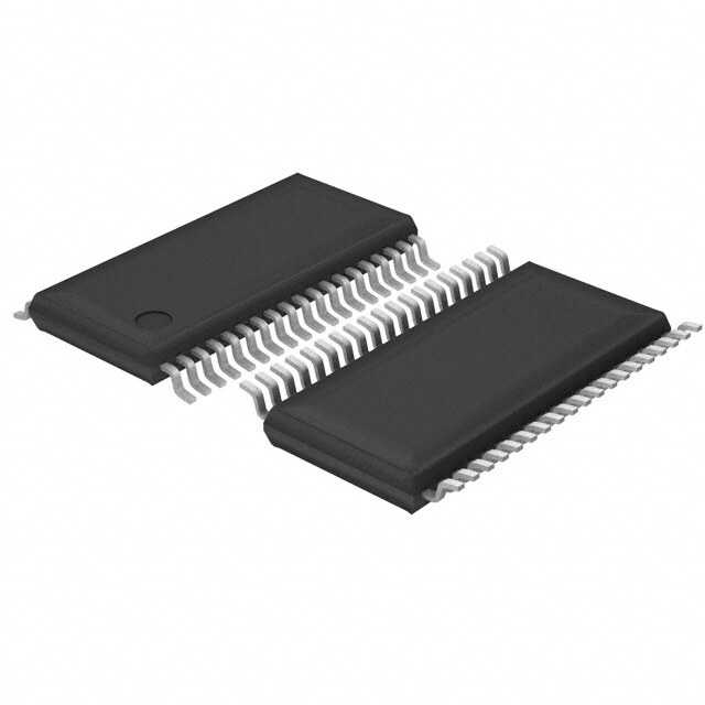
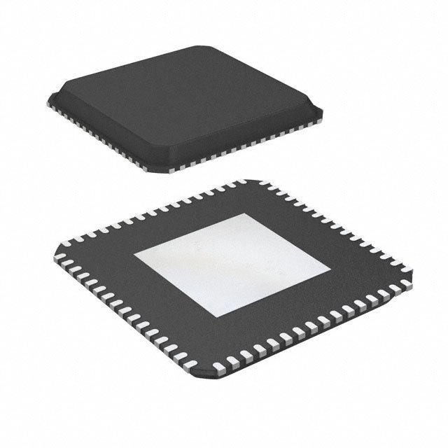
| 产品图片 |
|
| 产品型号 | AT91M40800-33AU-999 |
| RAM容量 | 8K x 8 |
| rohs | 无铅 / 符合限制有害物质指令(RoHS)规范要求 |
| 产品系列 | AT91 |
| 产品培训模块 | http://www.digikey.cn/PTM/IndividualPTM.page?site=cn&lang=zhs&ptm=24723http://www.digikey.cn/PTM/IndividualPTM.page?site=cn&lang=zhs&ptm=24997http://www.digikey.cn/PTM/IndividualPTM.page?site=cn&lang=zhs&ptm=26162http://www.digikey.cn/PTM/IndividualPTM.page?site=cn&lang=zhs&ptm=26159http://www.digikey.cn/PTM/IndividualPTM.page?site=cn&lang=zhs&ptm=26180 |
| 供应商器件封装 | * |
| 其它名称 | AT91M40800-33AU-999DKR |
| 包装 | Digi-Reel® |
| 外设 | POR,WDT |
| 封装/外壳 | 100-LQFP |
| 工作温度 | -40°C ~ 85°C |
| 振荡器类型 | 外部 |
| 数据转换器 | - |
| 标准包装 | 1 |
| 核心处理器 | ARM7® |
| 核心尺寸 | 16/32-位 |
| 电压-电源(Vcc/Vdd) | 1.8 V ~ 3.6 V |
| 程序存储器类型 | ROMless |
| 程序存储容量 | - |
| 连接性 | EBI/EMI,UART/USART |
| 速度 | 33MHz |


- 商务部:美国ITC正式对集成电路等产品启动337调查
- 曝三星4nm工艺存在良率问题 高通将骁龙8 Gen1或转产台积电
- 太阳诱电将投资9.5亿元在常州建新厂生产MLCC 预计2023年完工
- 英特尔发布欧洲新工厂建设计划 深化IDM 2.0 战略
- 台积电先进制程称霸业界 有大客户加持明年业绩稳了
- 达到5530亿美元!SIA预计今年全球半导体销售额将创下新高
- 英特尔拟将自动驾驶子公司Mobileye上市 估值或超500亿美元
- 三星加码芯片和SET,合并消费电子和移动部门,撤换高东真等 CEO
- 三星电子宣布重大人事变动 还合并消费电子和移动部门
- 海关总署:前11个月进口集成电路产品价值2.52万亿元 增长14.8%


PDF Datasheet 数据手册内容提取
Features • Incorporates the ARM7TDMI® ARM® Thumb® Processor Core – High-performance 32-bit RISC Architecture – High-density 16-bit Instruction Set – Leader in MIPS/Watt – Embedded ICE (In-Circuit Emulation) (cid:127) 8K Bytes On-chip SRAM – 32-bit Data Bus – Single-clock Cycle Access (cid:127) Fully-programmable External Bus Interface (EBI) AT91 – Maximum External Address Space of 64M Bytes – Up to 8 Chip Selects – Software Programmable 8-/16-bit External Data Bus ARM® Thumb® (cid:127) 8-level Priority, Individually Maskable, Vectored Interrupt Controller – 4 External Interrupts, Including a High-priority Low-latency Interrupt Request Microcontrollers (cid:127) 32 Programmable I/O Lines (cid:127) 3-channel 16-bit Timer/Counter – 3 External Clock Inputs – 2 Multi-purpose I/O Pins per Channel AT91M40800 (cid:127) 2 USARTs – 2 Dedicated Peripheral Data Controller (PDC) Channels per USART Electrical (cid:127) Programmable Watchdog Timer (cid:127) Advanced Power-saving Features Characterisitics – CPU and Peripheral Can be Deactivated Individually (cid:127) Fully Static Operation: 0 Hz to 40 MHz Internal Frequency Range at 3.0 V, 85°C (cid:127) 1.8V to 3.6V Operating Range (cid:127) Available in a 100-lead TQFP Package Description The AT91M40800 microcontroller is a member of the Atmel AT91 16-/32-bit microcon- troller family, which is based on the ARM7TDMI processor core. This processor has a high-performance 32-bit RISC architecture with a high-density 16-bit instruction set and very low power consumption. In addition, a large number of internally banked reg- isters result in very fast exception handling, making the device ideal for real-time control applications. The AT91M40800 microcontroller features a direct connection to off-chip memory, including Flash, through the fully-programmable External Bus Interface (EBI). An eight-level priority vectored interrupt controller, in conjunction with the Peripheral Data Controller, significantly improves the real-time performance of the device. The device is manufactured using Atmel’s high-density CMOS technology. By combin- ing the ARM7TDMI processor core with on-chip high-speed memory and a wide range of peripheral functions on a monolithic chip, the AT91M40800 is a powerful microcon- troller that offers a flexible, cost-effective solution to many compute-intensive embedded control applications. 1393C–ATARM–19-Nov-04
Absolute Maximum Ratings* Operating Temperature (Industrial).. -40°C to + 85°C *NOTICE: Stresses beyond those listed under “Absolute Maxi- mum Ratings” may cause permanent damage to the Storage Temperature ..................... -60°C to + 150°C device. This is a stress rating only and functional oper- ation of the device at these or other conditions beyond Voltage on Any Input Pin those indicated in the operational sections of this spec- with Respect to Ground......................-0.5V to + 5.5V ification is not implied. Exposure to absolute maximum rating conditions for extended periods may affect Maximum Operating Voltage................................4.6V device reliability. DC Output Current..............................................6 mA The following characteristics are applicable to the Operating Temperature range: T = -40°C to +85°C, unless otherwise A specified and are certified for a Junction Temperature up to T = 100°C. J Table 1. DC Characteristics Symbol Parameter Conditions Min Typ Max Units V DC Supply 1.8 3.6 V DD V Input Low Voltage V = 3.3V 0.8 V IL DD V Input High Voltage V = 3.3V 2.0 V IH DD V Output Low Voltage I = 2.0 mA, V = 3.3V 0.4 V OL OL DD V Output High Voltage I = 2.0 mA, V = 3.3V 2.4 V OH OH DD I Input Leakage Current 4 µA LEAK I Input Pull-up Current V = 3.6V, V = 0V 350 µA PULL DD IN C Input Capacitance 6.6 pF IN V = 3.6V; MCKI = 0 Hz T = 25°C 12.5 DD A I Static Current All inputs driven µA SC T = 85°C 250 TMS, TDI, TCK, NRST = 1 A AT91M40800 Electrical Characteristics 2 1393C–ATARM–19-Nov-04
AT91M40800 Electrical Characteristics Power Consumption The values in the following tables are measured values in the operating conditions indi- cated (i.e., V = 3.3V or 2.0V, T = 25°C) on the AT91EB40 Evaluation Board. DD A Table 2. Power Consumption V DD Mode Conditions 2.0V 3.3V Unit Reset 0.06 0.10 Fetch in ARM mode out of internal SRAM 1.38 4.63 All peripheral clocks activated Normal Fetch in ARM mode out of internal mW/MHz SRAM 1.04 3.44 All peripheral clocks deactivated All peripheral clocks activated 0.61 2.06 Idle All peripheral clocks deactivated 0.19 0.79 Table 3. Power Consumption per Peripheral V DD Peripheral 2.0V 3.3V Unit PIO Controller 0.01 0.16 Timer/Counter Channel 0.01 0.15 mW/MHz Timer/Counter Block (3 Channels) 0.02 0.35 USART 0.03 0.40 3 1393C–ATARM–19-Nov-04
Thermal and Reliability Considerations Thermal Data In Table 4, the device lifetime is estimated with the MIL-217 standard in the “moderately controlled” environmental model (this model is described as corresponding to an instal- lation in a permanent rack with adequate cooling air), depending on the device Junction Temperature. (For details see the section “Junction Temperature” on page 5.) Note that the user must be extremely cautious with this MTBF calculation: as the MIL- 217 model is pessimistic with respect to observed values due to the way the data/mod- els are obtained (test under severe conditions). The life test results that have been measured are always better than the predicted ones. Table 4. MTBF Versus Junction Temperature Junction Temperature (T ) (°C) Estimated Lifetime (MTBF) (Year) J 100 40 125 22 150 12 175 7 Table 5 summarizes the thermal resistance data related to the package of interest. Table 5. Thermal Resistance Data Symbol Parameter Condition Package Typ Unit θ Junction-to-ambient thermal Still Air TQFP100 40 JA resistance °C/ W θ Junction-to-case thermal resistance TQFP100 6.4 JC Reliability Data The number of gates and the device die size are provided for the user to calculate reli- ability data with another standard and/or in another environmental model. Table 6. Reliability Data Parameter Data Unit Number of Logic Gates 272 K gates Number of Memory Gates 400 K gates Device Die Size 17.6 mm2 AT91M40800 Electrical Characteristics 4 1393C–ATARM–19-Nov-04
AT91M40800 Electrical Characteristics Junction Temperature The average chip-junction temperature T in °C can be obtained from the following: J 1. T = T +(P × θ ) J A D JA 2. T = T +(P × (θ +θ )) J A D HEATSINK JC Where: (cid:127) θ = package thermal resistance, Junction-to-ambient (°C/W), provided in Table 5 JA on page 4. (cid:127) θ = package thermal resistance, Junction-to-case thermal resistance (°C/W), JC provided in Table 5 on page 4. (cid:127) θ = cooling device thermal resistance (°C/W), provided in the device HEAT SINK datasheet. (cid:127) P = device power consumption (W) estimated from data provided in the section D “Power Consumption” on page 3. (cid:127) T = ambient temperature (°C). A From the first equation, the user can derive the estimated lifetime of the chip and thereby decide if a cooling device is necessary or not. If a cooling device is to be fitted on the chip, the second equation should be used to compute the resulting average chip- junction temperature T in °C. J 5 1393C–ATARM–19-Nov-04
Conditions Timing Results The delays are given as typical values in the following conditions: (cid:127) V = 3.3V DD (cid:127) Ambient Temperature = 25°C (cid:127) Load Capacitance = 0 pF (cid:127) The output level change detection is 0.5 x V DD (cid:127) The input level is 0.3 x V for a low-level detection and is 0.7 x V for a high level DD DD detection. The minimum and maximum values given in the AC characteristics tables of this datasheet take into account the process variation and the design. In order to obtain the timing for other conditions, the following equation should be used: t = δ × δ × (t +∑(C × δ )) T° VDD DATASHEET SIGNAL CSIGNAL Where: (cid:127) δ° is the derating factor in temperature given in Figure 1. T (cid:127) δ is the derating factor for the Power Supply given in Figure 2. VDD (cid:127) t is the minimum or maximum timing value given in this datasheet for a load DATASHEET capacitance of 0 pF. (cid:127) C is the capacitance load on the considered output pin.(1) SIGNAL (cid:127) δ is the load derating factor depending on the capacitance load on the related CSIGNAL output pins given in Min and Max values in this datasheet. The input delays are given as typical values. The input delays are given as typical value. Note: 1. The user must take into account the package capacitance load contribution (C ) IN described in Table 1 on page 2. Temperature Derating Figure 1. Derating Curve for Different Operating Temperatures Factor 1.3 1.2 or ct a 1.1 F g n ati er 1 D Derating Factor for 0.9 Typ Case is 1 0.8 -60 -40 -20 0 20 40 60 80 100 120 140 160 Operating Temperature (˚C) AT91M40800 Electrical Characteristics 6 1393C–ATARM–19-Nov-04
AT91M40800 Electrical Characteristics Supply Voltage Derating Figure 2. Derating Curve for Different Supply Voltages Factor 1.70 1.65 1.60 1.55 Typical Derating Factor 1.50 for Typ Case is 1 1.45 r cto 1.40 a 1.35 F g 1.30 n ati 1.25 er 1.20 D 1.15 1.10 1.05 1.00 0.95 0.90 2.0 2.2 2.4 2.6 2.8 3.0 3.2 3.4 3.6 Supply Voltage (V) Note: This derating factor is applicable only to timings related to output pins. 7 1393C–ATARM–19-Nov-04
Clock Waveforms Table 7. Master Clock Waveform Parameters Symbol Parameter Conditions Min Max Units 1/(t ) Oscillator Frequency 47.7 MHz CP t Oscillator Period 21.0 ns CP t High Half-period 9.1 ns CH t Low Half-period 9.4 ns CL Table 8. Clock Propagation Times Symbol Parameter Conditions Min Max Units C = 0 pF 4.2 6.6 ns MCKO t Rising Edge Propagation Time CDLH C derating 0.034 0.053 ns/pF MCKO C = 0 pF 4.5 7.1 ns MCKO t Falling Edge Propagation Time CDHL C derating 0.042 0.066 ns/pF MCKO Figure 3. Clock Waveform t CH MCKI 0.7 V DD 0.3 V DD t CL t CP 0.5 V 0.5 V DD DD MCKO t t CDLH CDHL AT91M40800 Electrical Characteristics 8 1393C–ATARM–19-Nov-04
AT91M40800 Electrical Characteristics Table 9. NRST to MCKO Symbol Parameter Min Max Units t NRST Rising Edge to MCKO Valid 3(t /2) 7(t /2) ns D CP CP Time Figure 4. MCKO Relative to NRST NRST t D MCKO 9 1393C–ATARM–19-Nov-04
AC Characteristics EBI Signals Relative to MCKI The following tables show timings relative to operating condition limits defined in the section “Timing Results” on page 6. See Figure 5 on page 14. Table 10. General-purpose EBI Signals Symbol Parameter Conditions Min Max Units C = 0 pF 5.4 11.7 ns NUB EBI MCKI Falling to NUB Valid 1 C derating 0.034 0.066 ns/pF NUB C = 0 pF 4.3 8.7 ns NLB EBI MCKI Falling to NLB/A0 Valid 2 C derating 0.038 0.062 ns/pF NLB C = 0 pF 4.2 10.0 ns ADD EBI MCKI Falling to A1 - A23 Valid 3 C = derating 0.038 0.066 ns/pF ADD MCKI Falling to Chip Select CNCS = 0 pF 4.6 10.4 ns EBI 4 Change C derating 0.038 0.057 ns/pF NCS EBI NWAIT Setup before MCKI Rising 0.6 ns 5 EBI NWAIT Hold after MCKI Rising 3.2 ns 6 AT91M40800 Electrical Characteristics 10 1393C–ATARM–19-Nov-04
AT91M40800 Electrical Characteristics Table 11. EBI Write Signals Symbol Parameter Conditions Min Max Units C = 0 pF 4.3 7.1 ns NWR EBI MCKI Rising to NWR Active (No Wait States) 7 C derating 0.042 0.066 ns/pF NWR C = 0 pF 5.0 8.2 ns NWR EBI MCKI Rising to NWR Active (Wait States) 8 C derating 0.042 0.066 ns/pF NWR C = 0 pF 4.9 8.0 ns NWR EBI MCKI Falling to NWR Inactive (No Wait States) 9 C derating 0.034 0.053 ns/pF NWR C = 0 pF 5.0 8.2 ns NWR EBI MCKI Rising to NWR Inactive (Wait States) 10 C derating 0.034 0.053 ns/pF NWR C = 0 pF 4.1 8.6 ns DATA EBI MCKI Rising to D0 - D15 Out Valid 11 C derating 0 0.066 ns/pF DATA C = 0 pF 3.3 7.6 ns NUB EBI NWR High to NUB Change 12 C derating 0.034 0.066 ns/pF NUB C = 0 pF 2.8 4.6 ns NLB EBI NWR High to NLB/A0 Change 13 C derating 0.042 0.066 ns/pF NLB C = 0 pF 2.7 6.5 ns ADD EBI NWR High to A1 - A23 Change 14 C derating 0.042 0.066 ns/pF ADD C = 0 pF 3.2 6.4 ns NCS EBI NWR High to Chip Select Inactive 15 C derating 0.034 0.066 ns/pF NCS C = 0 pF t - 0.9 ns CH EBI Data Out Valid before NWR High (No Wait States)(1) C derating -0.066 ns/pF 16 DATA C derating 0.053 ns/pF NWR C = 0 pF n x t - 0.8(2) ns CP EBI Data Out Valid before NWR High (Wait States)(1) C derating -0.066 ns/pF 17 DATA C derating 0.053 ns/pF NWR EBI Data Out Valid after NWR High 2.1 ns 18 C = 0 pF t + 0.4 ns EBI NWR Minimum Pulse Width (No Wait States)(1) NWR CH 19 C derating -0.013 ns/pF NWR C = 0 pF n x t - 0.4(2) ns EBI NWR Minimum Pulse Width (Wait States)(1) NWR CP 20 C derating -0.013 ns/pF NWR Notes: 1. The derating factor should not be applied to t or t . CH CP 2. n = number of standard wait states inserted. 11 1393C–ATARM–19-Nov-04
Table 12. EBI Read Signals Symbol Parameter Conditions Min Max Units C = 0 pF 5.0 9.0 ns EBI MCKI Falling to NRD Active(1) NRD 21 C derating 0.042 0.066 ns/pF NRD C = 0 pF 4.1 8.6 ns EBI MCKI Rising to NRD Active(2) NRD 22 C derating 0.042 0.066 ns/pF NRD C = 0 pF 5.2 9.4 ns EBI MCKI Falling to NRD Inactive(1) NRD 23 C derating 0.034 0.053 ns/pF NRD C = 0 pF 4.9 7.7 ns EBI MCKI Falling to NRD Inactive(2) NRD 24 C derating 0.034 0.053 ns/pF NRD EBI D0 - D15 In Setup before MCKI Falling Edge(5) -0.3 ns 25 EBI D0 - D15 In Hold after MCKI Falling Edge(5) 4.0 ns 26 C = 0 pF 4.1 8.4 ns NUB EBI NRD High to NUB Change 27 C derating 0.034 0.066 ns/pF NUB C = 0 pF 3.3 5.2 ns NLB EBI NRD High to NLB/A0 Change 28 C derating 0.042 0.066 ns/pF NLB C = 0 pF 3.2 7.1 ns ADD EBI NRD High to A1 - A23 Change 29 C derating 0.042 0.066 ns/pF ADD C = 0 pF 3.6 6.9 ns NCS EBI NRD High to Chip Select Inactive 30 C derating 0.034 0.066 ns/pF NCS C = 0 pF 9.0 ns EBI Data Setup before NRD High(5) NRD 31 C derating 0.053 ns/pF NRD C = 0 pF -2.4 ns EBI Data Hold after NRD High(5) NRD 32 C derating -0.034 ns/pF NRD C = 0 pF (n +1) t - 0.7(4) ns EBI NRD Minimum Pulse Width(1)(3) NRD CP 33 C derating -0.013 ns/pF NRD C = 0 pF n x t + (t - 0.9)(4) ns EBI NRD Minimum Pulse Width(2)(3) NRD CP CH 34 C derating -0.013 ns/pF NRD Notes: 1. Early Read Protocol. 2. Standard Read Protocol. 3. The derating factor should not be applied to t or t . CH CP 4. n = number of standard wait states inserted. 5. Only one of these two timings needs to be met. AT91M40800 Electrical Characteristics 12 1393C–ATARM–19-Nov-04
AT91M40800 Electrical Characteristics Table 13. EBI Read and Write Control Signals. Capacitance Limitation Symbol Parameter Conditions Min Max Units C = 0 pF 10.8 ns T (1) Master Clock Low Due to NRD Capacitance NRD CPLNRD C derating 0.053 ns/pF NRD C = 0 pF 8.6 ns T (2) Master CLock Low Due to NWR Capacitance NWR CPLNWR C derating 0.053 ns/pF NWR Notes: 1. If this condition is not met, the action depends on the read protocol intended for use. (cid:127) Early Read Protocol: Programing an additional t (Data Float Output Time) cycle. DF (cid:127) Standard Read Protocol: Programming an additional t Cycle and an additional wait state. DF 2. Applicable only for chip select programmed with 0 wait state. If this condition is not met, at least one wait state must be programmed. 13 1393C–ATARM–19-Nov-04
Figure 5. EBI Signals Relative to MCKI MCKI EBI EBI 4 4 NCS CS EBI 3 A1 - A23 EBI EBI 5 6 NWAIT EBI /EBI 1 2 NUB/NLB/A0 EBI 21 EBI EBI 23 27 - 30 EBI 33 NRD(1) EBI EBI 22 24 NRD(2) EBI34 EBI EBI 31 32 EBI EBI 25 26 D0 - D15 Read EBI7 EBI9 EBI12 - 15 NWR (No Wait States) EBI19 EBI EBI 8 10 NWR (Wait States) EBI20 EBI EBI EBI 11 17 18 EBI EBI 16 18 D0 - D15 to Write No Wait Wait Notes: 1. Early Read Protocol. 2. Standard Read Protocol. AT91M40800 Electrical Characteristics 14 1393C–ATARM–19-Nov-04
AT91M40800 Electrical Characteristics Peripheral Signals USART Signals The inputs have to meet the minimum pulse width and period constraints shown in Table 14 and Table 15, and represented in Figure 6. Table 14. USART Input Minimum Pulse Width Symbol Parameter Min Pulse Width Units US SCK/RXD Minimum Pulse Width 5(t /2) ns 1 CP Table 15. USART Minimum Input Period Symbol Parameter Min Input Period Units US SCK Minimum Input Period 9(t /2) ns 2 CP Figure 6. USART Signals US 1 RXD US 2 US 1 SCK 15 1393C–ATARM–19-Nov-04
Timer/Counter Signals Due to internal synchronization of input signals, there is a delay between an input event and a corresponding output event. This delay is 3(t ) in Waveform Event Detection CP mode and 4(t ) in Waveform Total-count Detection mode. The inputs have to meet the CP minimum pulse width and minimum input period shown in Table 16 and Table 17, and as represented in Figure 7. Table 16. Timer Input Minimum Pulse Width Symbol Parameter Min Pulse Width Units TC TCLK/TIOA/TIOB Minimum Pulse Width 3(t /2) ns 1 CP Table 17. Timer Input Minimum Period Symbol Parameter Min Input Period Units TC TCLK/TIOA/TIOB Minimum Input Period 5(t /2) ns 2 CP Figure 7. Timer Input TC 2 3(t /2) 3(t /2) CP CP MCKI TC 1 TIOA/ TIOB/ TCLK AT91M40800 Electrical Characteristics 16 1393C–ATARM–19-Nov-04
AT91M40800 Electrical Characteristics Reset Signals A minimum pulse width is necessary, as shown in Table 18 and as represented in Fig- ure 8. Table 18. Reset Minimum Pulse Width Symbol Parameter Min Pulse-width Units RST NRST Minimum Pulse Width 10(t ) ns 1 CP Figure 8. Reset Signal RST 1 NRST Only the NRST rising edge is synchronized with MCKI. The falling edge is asynchronous. 17 1393C–ATARM–19-Nov-04
Advanced Interrupt Controller Inputs have to meet the minimum pulse width and minimum input period shown in Table Signals 19 and Table 20 and represented in Figure 9. Table 19. AIC Input Minimum Pulse Width Symbol Parameter Min Pulse Width Units AIC FIQ/IRQ0/IRQ1/IRQ2/IRQ3 Minimum Pulse Width 3(t /2) ns 1 CP Table 20. AIC Input Minimum Period Symbol Parameter Min Input Period Units AIC AIC Minimum Input Period 5(t /2) ns 2 CP Figure 9. AIC Signals AIC 2 MCKI FIQ/ AIC1 IRQ0/IRQ1/ IRQ2/IRQ3 Input Parallel I/O Signals The inputs have to meet the minimum pulse width shown in Table 21 and represented in Fig- ure 10. Table 21. PIO Input Minimum Pulse Width Symbol Parameter Min Pulse Width Units PIO PIO Input Minimum Pulse Width 3(t /2) ns 1 CP Figure 10. PIO Signal PIO 1 PIO Inputs AT91M40800 Electrical Characteristics 18 1393C–ATARM–19-Nov-04
AT91M40800 Electrical Characteristics ICE Interface Signals Table 22. ICE Interface Timing Specifications Symbol Parameter Conditions Min Max Units ICE NTRST Minimum Pulse Width 18.8 ns 0 ICE NTRST High Recovery to TCK High 1.2 ns 1 NTRST High Removal from TCK ICE 2 High -0.2 ns ICE TCK Low Half-period 41.7 ns 3 ICE TCK High Half-period 40.9 ns 4 ICE TCK Period 82.5 ns 5 ICE TDI, TMS Setup before TCK High 0.5 ns 6 ICE TDI, TMS Hold after TCK High 0.6 ns 7 C = 0 pF 5.2 ns TDO ICE TDO Hold Time 8 C derating 0 ns/pF TDO C = 0 pF 10.2 ns TDO ICE TCK Low to TDO Valid 9 C derating 0.063 ns/pF TDO Figure 11. ICE Interface Signal ICE 0 NTRST ICE1 ICE2 ICE 5 TCK ICE ICE 3 4 TMS/TDI ICE ICE 6 7 TDO ICE 8 ICE 9 19 1393C–ATARM–19-Nov-04
Document Details Title AT91M40800 Electrical Characteristics Literature Number Lit# 1393B Revision History Version A Publication Date: Sep, 2000 Version B Publication Date: 10-Dec-2001 Revisions Since Previous Version published on Intranet Page: 1 “Features” “Fully Static Operation: 0 Hz to 40 MHz Internal Frequency Range at 3.0 V, 85°C” ..... frequency and range modified Page: 4 “Reliability Data” paragraph modified and new table inserted. “Table 6 Reliability Data” Page: 6 “Timing Results” Cross reference added to C part of equation. SIGNAL Page: 8 Table 7. Master Clock Waveform Parameters. Values have been changed for Oscillator Frequency and Oscillator Period. Some master clock parameters deleted. Page: 10 Table 10. General-purpose EBI Signals. EBI , Conditions are changed. 4 Page: 13 New table inserted. Table 13. Read and Write Control Signals. Capacitance Limitation. This table adds understanding to EBI Signals Relative to MCK. Version C Publication Date: 19-Nov-2004 Page 8 Changes in Table 7: new figures for t and t , removed references to t and t. Updated CH CL r f Figure 3 on page 8. AT91M40800 Electrical Characteristics 20 1393C–ATARM–19-Nov-04
Atmel Corporation Atmel Operations 2325 Orchard Parkway Memory RF/Automotive San Jose, CA 95131, USA 2325 Orchard Parkway Theresienstrasse 2 Tel: 1(408) 441-0311 San Jose, CA 95131, USA Postfach 3535 Fax: 1(408) 487-2600 Tel: 1(408) 441-0311 74025 Heilbronn, Germany Fax: 1(408) 436-4314 Tel: (49) 71-31-67-0 Fax: (49) 71-31-67-2340 Regional Headquarters Microcontrollers Europe 2325 Orchard Parkway 1150 East Cheyenne Mtn. Blvd. Atmel Sarl San Jose, CA 95131, USA Colorado Springs, CO 80906, USA Route des Arsenaux 41 Tel: 1(408) 441-0311 Tel: 1(719) 576-3300 Case Postale 80 Fax: 1(408) 436-4314 Fax: 1(719) 540-1759 CH-1705 Fribourg La Chantrerie Biometrics/Imaging/Hi-Rel MPU/ Switzerland BP 70602 High Speed Converters/RF Datacom Tel: (41) 26-426-5555 Fax: (41) 26-426-5500 44306 Nantes Cedex 3, France Avenue de Rochepleine Tel: (33) 2-40-18-18-18 BP 123 Asia Fax: (33) 2-40-18-19-60 38521 Saint-Egreve Cedex, France Room 1219 Tel: (33) 4-76-58-30-00 Chinachem Golden Plaza ASIC/ASSP/Smart Cards Fax: (33) 4-76-58-34-80 Zone Industrielle 77 Mody Road Tsimshatsui 13106 Rousset Cedex, France East Kowloon Tel: (33) 4-42-53-60-00 Hong Kong Fax: (33) 4-42-53-60-01 Tel: (852) 2721-9778 Fax: (852) 2722-1369 1150 East Cheyenne Mtn. Blvd. Japan Colorado Springs, CO 80906, USA 9F, Tonetsu Shinkawa Bldg. Tel: 1(719) 576-3300 1-24-8 Shinkawa Fax: 1(719) 540-1759 Chuo-ku, Tokyo 104-0033 Scottish Enterprise Technology Park Japan Maxwell Building Tel: (81) 3-3523-3551 Fax: (81) 3-3523-7581 East Kilbride G75 0QR, Scotland Tel: (44) 1355-803-000 Fax: (44) 1355-242-743 Literature Requests www.atmel.com/literature Disclaimer: The information in this document is provided in connection with Atmel products. No license, express or implied, by estoppel or otherwise, to any intellectual property right is granted by this document or in connection with the sale of Atmel products. EXCEPT AS SET FORTH IN ATMEL’S TERMS AND CONDI- TIONS OF SALE LOCATED ON ATMEL’S WEB SITE, ATMEL ASSUMES NO LIABILITY WHATSOEVER AND DISCLAIMS ANY EXPRESS, IMPLIED OR STATUTORY WARRANTY RELATING TO ITS PRODUCTS INCLUDING, BUT NOT LIMITED TO, THE IMPLIED WARRANTY OF MERCHANTABILITY, FITNESS FOR A PARTICULAR PURPOSE, OR NON-INFRINGEMENT. IN NO EVENT SHALL ATMEL BE LIABLE FOR ANY DIRECT, INDIRECT, CONSEQUENTIAL, PUNITIVE, SPECIAL OR INCIDEN- TAL DAMAGES (INCLUDING, WITHOUT LIMITATION, DAMAGES FOR LOSS OF PROFITS, BUSINESS INTERRUPTION, OR LOSS OF INFORMATION) ARISING OUT OF THE USE OR INABILITY TO USE THIS DOCUMENT, EVEN IF ATMEL HAS BEEN ADVISED OF THE POSSIBILITY OF SUCH DAMAGES. Atmel makes no representations or warranties with respect to the accuracy or completeness of the contents of this document and reserves the right to make changes to specifications and product descriptions at any time without notice. Atmel does not make any commitment to update the information contained herein. Atmel’s products are not intended, authorized, or warranted for use as components in applications intended to support or sustain life. © Atmel Corporation 2004. All rights reserved. Atmel®, logo and combinations thereof are registered trademarks, and Everywhere You AreSM is the trademark of Atmel Corporation or its subsidiaries. ARM®, Thumb® and ARM7TDMI® are registered trademarks of ARM Ltd. Other terms and product names may be trademarks of others. Printed on recycled paper. 1393C–ATARM–19-Nov-04
Mouser Electronics Authorized Distributor Click to View Pricing, Inventory, Delivery & Lifecycle Information: M icrochip: AT91M40800-33AU AT91M40800-33AU-999