ICGOO在线商城 > 射频/IF 和 RFID > RFID,RF 接入,监控 IC > AT88RF1354-ZU
 Datasheet下载
- 型号: AT88RF1354-ZU
- 制造商: Atmel
- 库位|库存: xxxx|xxxx
- 要求:
| 数量阶梯 | 香港交货 | 国内含税 |
| +xxxx | $xxxx | ¥xxxx |
查看当月历史价格
查看今年历史价格
AT88RF1354-ZU产品简介:
ICGOO电子元器件商城为您提供AT88RF1354-ZU由Atmel设计生产,在icgoo商城现货销售,并且可以通过原厂、代理商等渠道进行代购。 AT88RF1354-ZU价格参考。AtmelAT88RF1354-ZU封装/规格:RFID,RF 接入,监控 IC, RFID Reader IC 13.56MHz ISO 14443 SPI 3 V ~ 3.6 V 36-VFQFN Exposed Pad。您可以下载AT88RF1354-ZU参考资料、Datasheet数据手册功能说明书,资料中有AT88RF1354-ZU 详细功能的应用电路图电压和使用方法及教程。
Microchip Technology的AT88RF1354-ZU是一款集成RFID和射频接入功能的监控IC,主要应用于需要非接触式识别与安全通信的场景。该芯片支持ISO/IEC 14443 Type A/B协议,适用于13.56MHz高频RFID系统,具备读写器和标签的双向通信能力。

典型应用场景包括:

1. 门禁控制系统:用于智能门锁、办公室或住宅的安全访问控制,通过RFID卡或手机NFC实现安全认证。
2. 电子支付终端:作为POS终端中的关键组件,支持非接触式支付功能,提升交易效率与用户体验。
3. 公共交通票务系统:用于地铁、公交等自动售检票系统,实现快速、安全的刷卡通行。
4. 资产追踪与管理:在物流、医疗或仓储领域中,对高价值设备或物品进行实时追踪与身份验证。
5. 智能家电与物联网设备:用于家电的身份识别与权限管理,如智能洗衣机识别专用会员卡,或智能家居设备之间的安全配对。

AT88RF1354-ZU集成了加密引擎,支持多种安全算法,确保数据传输的保密性与完整性,适合对安全性要求较高的应用场合。
| 参数 | 数值 |
| 产品目录 | |
| 描述 | IC RF READER 13.56MHZ 36-VQFNRFID应答器 14443, Type B RFID Reader |
| 产品分类 | RFID IC集成电路 - IC |
| 品牌 | Atmel |
| 产品手册 | |
| 产品图片 |
|
| rohs | 符合RoHS无铅 / 符合限制有害物质指令(RoHS)规范要求 |
| 产品系列 | RF集成电路,RFID应答器,Atmel AT88RF1354-ZU- |
| 数据手册 | |
| 产品型号 | AT88RF1354-ZU |
| PCN其它 | |
| RF类型 | - |
| 产品种类 | RFID应答器 |
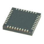
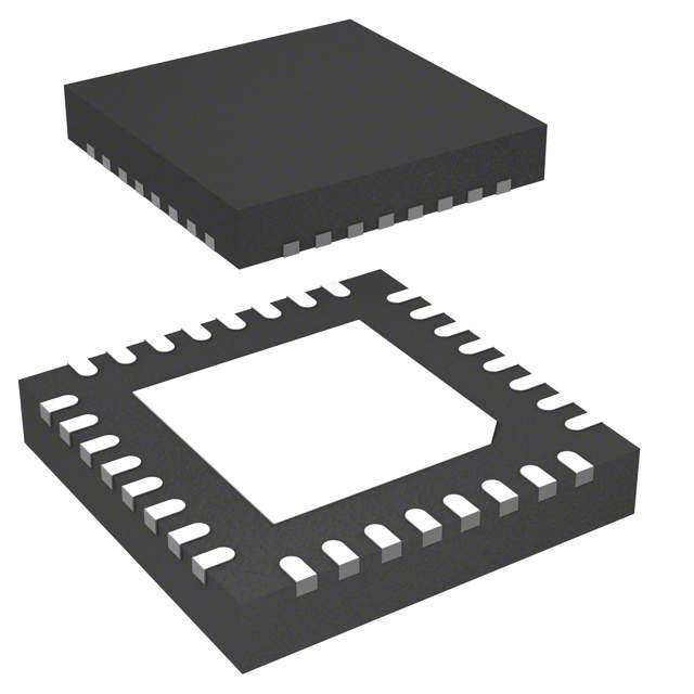
| 供应商器件封装 | 36-QFN-EP(6x6) |
| 其它名称 | AT88RF1354ZU |
| 功能 | Type B RF Reader |
| 包装 | 托盘 |
| 商标 | Atmel |
| 安装风格 | SMD/SMT |
| 封装/外壳 | 36-VFQFN 裸露焊盘 |
| 封装/箱体 | QFN-36 |
| 工作温度范围 | - 40 C to + 85 C |
| 工厂包装数量 | 980 |
| 最大工作温度 | + 85 C |
| 最小工作温度 | - 40 C |
| 标准包装 | 980 |
| 特性 | ISO14443-B |
| 频率 | 13.56 MHz |


- 商务部:美国ITC正式对集成电路等产品启动337调查
- 曝三星4nm工艺存在良率问题 高通将骁龙8 Gen1或转产台积电
- 太阳诱电将投资9.5亿元在常州建新厂生产MLCC 预计2023年完工
- 英特尔发布欧洲新工厂建设计划 深化IDM 2.0 战略
- 台积电先进制程称霸业界 有大客户加持明年业绩稳了
- 达到5530亿美元!SIA预计今年全球半导体销售额将创下新高
- 英特尔拟将自动驾驶子公司Mobileye上市 估值或超500亿美元
- 三星加码芯片和SET,合并消费电子和移动部门,撤换高东真等 CEO
- 三星电子宣布重大人事变动 还合并消费电子和移动部门
- 海关总署:前11个月进口集成电路产品价值2.52万亿元 增长14.8%


PDF Datasheet 数据手册内容提取
Features • Compatible with all ISO/IEC 14443 Type B Compliant Cards, Tags, and Transponders • High Performance 13.56 MHz RF Communications Interface ⎯ ISO/IEC 14443-2 Type B Compliant 106 Kbps Signaling ⎯ ISO/IEC 14443-3 Type B Compliant Frame and Data Format Internal Transmitter Drives Antenna with No External Active Circuitry 13.56 MHz Type B ⎯ Robust Receiver Demodulates and Decodes Type B Signals RF Reader • Intelligent RF Reader Functions ⎯ ISO/IEC 14443-3 Type B Polling Function Specification ⎯ Type B Frame Formatting and Decoding is Handled Internally ⎯ Internal CRC Generation and Error Detection AT88RF1354 ⎯ Adjustable Frame Wait Timing ⎯ Internal Data Buffer • Two Serial Communication Interface Options ⎯ Two-Wire Interface (TWI) Slave Device with Clock Speed up to 1 MHz ⎯ SPI Mode 0 Slave Device with Clock Speed up to 2 MHz ⎯ SPI or TWI Mode Selection with Interface Mode Select Pin • Compatible with 3.3 V and 5 V Microcontrollers ⎯ Supply Voltage: 3.0 to 3.6 Volts or 4.5 to 5.5 Volts • Package: 6 by 6 mm QFN, Green compliant (exceeds RoHS) • Industrial Operating Temperature: -40° to +85° C Description The AT88RF1354 is a smart, high performance ISO/IEC 14443 Type B RF Reader IC. The AT88RF1354 communicates with RFID Transponders or Contactless Smartcards using the industry standard ISO/IEC 14443-2 Type B signal modulation scheme and ISO/IEC 14443-3 Type B frame format. Data is exchanged half duplex at a 106k bit per second rate. A two byte CRC_B provides communication error detection capability. The AT88RF1354 is compatible with 3.3 V and 5 V host microcontrollers with two-wire or SPI serial interfaces. In two-wire interface mode the AT88RF1354 operates as a TWI slave and requires four microcontroller pins for data communication and handshaking. In SPI interface mode the AT88RF1354 operates as a mode 0 SPI slave and requires six microcontroller pins for data communication and handshaking. To communicate with an RFID transponder the host microcontroller sends a data packet for transmission over the RF communications channel, and receives the response data packet that is received from the transponder over the RF communications channel. AT88RF1354 performs all RF communication packet formatting, decoding, and communication error checking. The host microcontroller is not burdened with RF encoding, timing, or protocol functions since these tasks are all performed by the AT88RF1354. 8547B–RFID–3/09
1. Introduction 1.1. Block Diagram Figure 1. Block Diagram RFin Filter C6 Modulator Transmit Receive ANT SRAM Command and Response Vss_ANT ANT Driver Logic Registers PLL 13.56 MHz Serial Interface CLKO Xtal1 Xtal2 ResetB ISEL Istat SSB SCK SDI SDO ADDR 13.56 MHz Type B RF Reader Specification 2 8547B–RFID–3/09
13.56 MHz Type B RF Reader Specification 1.2. System Diagram Figure 2. Communications in an RFID System Host Serial Interface Reader IC RFCommunications Card Microcontroller 1.3. Scope This AT88RF1354 Specification document contains the electrical and mechanical specifications for the AT88RF1354 RF Reader IC. The AT88RF1354 Command Reference Guide document contains detailed command and register specifications for the AT88RF1354 RF Reader. The AT88RF1354 Command Reference Guide is a reference for software developers and embedded systems programmers using the AT88RF1354 Reader. Reference Designs and additional technical information is available in AT88RF1354 Application Notes. The reference designs described in the AT88RF1354 Application Notes include schematics, board designs, and a complete bill of materials. Each reference design has been optimized for reliable, robust communications with cards and tags with antenna dimensions within a specified size range. See www.atmel.com 1.4. Conventions ISO/IEC 14443 nomenclature is used in this document where applicable. The following terms and abbreviations are utilized throughout this document. Additional terms are defined in the section in which they are used, or in 0. Card: A Contactless Smart Card or RFID Tag in proximity to the reader antenna. Host: The microcontroller connected to the serial interface of the reader IC. PCD: Proximity Coupling Device – is the host and reader with antenna. PICC: Proximity Integrated Circuit Card – is the tag/card containing an IC and antenna. Reader: The AT88RF1354 IC with loop antenna and associated circuitry RFU: Reserved for Future Use – is any feature, memory location, or bit that is held as reserved for future use by the ISO standards committee or by Atmel. $ xx: Hexadecimal Number – denotes a hex number “xx” (Most Significant Bit on left). xxxx b: Binary Number – denotes a binary number “xxxx” (Most Significant Bit on left). See Atmel Application Note Understanding the Requirements of ISO/IEC 14443 for Type B Proximity Contactless Identification Cards (doc 2056x) at www.atmel.com for detailed information regarding the ISO/IEC 14443 RF communication protocol. 3 8547B–RFID–3/09
2. Instruction Set Table 1. Instruction Set Sorted by Command Name Command Name Description Code Abort Exit command in progress $0D Clear Exit command in progress, Clear Buffer, Turn RF OFF $0E Poll Continuous Poll Continuously for Type B PICCs $02 Poll Single Poll Once for Type B PICCs $01 Read Buffer Read Data Buffer $08 Read Register Read Configuration Register $07 RF OFF Turn off 13.56 MHz RF Field $0B RF ON Turn on 13.56 MHz RF Field $0A Sleep Activate standby mode $0C TX Data Transmit data to PICC and receive the response $03 Write Buffer Write data buffer $09 Write Register Write configuration register $06 All other command code values are not supported The AT88RF1354 Command Reference Guide document contains all of the detailed information required by a software developer or embedded systems programmer to use the AT88RF1354 Instruction Set. See www.atmel.com for the AT88RF1354 Command Reference Guide (doc 5150x). 2.1. RF Communication Commands The RF ON Command and RF OFF Command are used to enable and disable the 13.56 MHz RF Field transmitter. The RF Field is turned on at the beginning of a transaction and off at the end, since ISO/IEC 14443 cards and tags are powered by the RF Field. The Poll Continuous Command or Poll Single Command is used to search for ISO/IEC 14443 cards in the RF Field using the standard REQB/WUPB and Slot-MARKER commands. These commands automatically perform the time-slot polling function described in ISO/IEC 14443 part 3, and return the response from the first card found to the host microcontroller. All other RF communication is performed with the TX Data Command. The RF command and data bytes to be transmitted are sent by the host microcontroller with the TX Data Command to AT88RF1354. The bytes received from the host are formatted into a Type B standard frame and transmitted on the RF communications channel, along with the CRC. When a response is received from the card, the response frame is decoded by AT88RF1354 and the resulting bytes are stored in SRAM buffer memory. If a CRC or frame format error is detected in the response, then bits are set in the Error Register (EREG). After the entire frame has been decoded by AT88RF1354, the host microcontroller reads the TX Data Response over the serial interface. 2.2. Reader Configuration Commands The Read Register Command and Write Register Command are used to read and write the configuration and status registers of the AT88RF1354. Both the Transmitter Register (TXC) and Receiver Register (RXC) must be configured before any RF communication occurs. The Sleep Command is used to put the AT88RF1354 into Standby Mode. In Standby Mode the internal circuitry is placed in standby, and all internal clocks are stopped. 13.56 MHz Type B RF Reader Specification 4 8547B–RFID–3/09
13.56 MHz Type B RF Reader Specification 2.3. Other Commands The Abort Command can be used to interrupt a Poll Single, Poll Continuous, or TX Data operation that is in progress. If a Poll Continuous Command is sent but there is no card in the field, then an Abort Command is used to interrupt the infinite polling loop. All other commands will timeout if no response is received, so it is usually not necessary to use the Abort Command to interrupt them. The Clear Command is used to clear the configuration registers and place AT88RF1354 in a known initial state. The Clear Command is usually the first command sent after the reader is powered on and reset. The Read Buffer Command and Write Buffer Command can be used to read and write the SRAM buffer that is used to store RF commands and RF responses. These commands are never required to be used during normal operation of the AT88RF1354. However, these commands are helpful for testing the integrity of the serial communications channel during system development. 5 8547B–RFID–3/09
3. Register Summary The AT88RF1354 Command Reference Guide document contains all of the detailed information required by a software developer or embedded systems programmer to use the AT88RF1354 Register Set. See www.atmel.com for the AT88RF1354 Command Reference Guide (doc 5150x). Table 2. Register set sorted by address. Register Register Description Register Type Name Address CPR0_L $00 (Default) Communication Protocol Register 0 - Low Byte Read-only CPR0_H $01 (Default) Communication Protocol Register 0 - High Byte Read-only CPR1_L $02 Communication Protocol Register 1 - Low Byte [RFU] Read / Write CPR1_H $03 Communication Protocol Register 1 - High Byte Read / Write CPR2_L $04 Communication Protocol Register 2 - Low Byte [RFU] Read / Write CPR2_H $05 Communication Protocol Register 2 - High Byte Read / Write CPR3_L $06 Communication Protocol Register 3 - Low Byte [RFU] Read / Write CPR3_H $07 Communication Protocol Register 3 - High Byte Read / Write CPR4_L $08 Communication Protocol Register 4 - Low Byte [RFU] Read / Write CPR4_H $09 Communication Protocol Register 4 - High Byte Read / Write SREG $0A Status Register Read-only EREG $0B Error Register Read-only IDR $0C Hardware ID Register Read-only PLL $0D PLL Output Configuration Register Read / Write TXC $0E Transmitter Register Read / Write RXC $0F Receiver Register Read / Write All other register address values are not supported 13.56 MHz Type B RF Reader Specification 6 8547B–RFID–3/09
13.56 MHz Type B RF Reader Specification The Register Memory Map in Table 3 shows the field names for each register bit. Read-only registers are colored yellow. Read/Write registers are colored green. Any bit identified as RFU or Reserved for Future Use is reserved for future definition by Atmel; these bits must always remain 0 b. Table 3. Register Memory Map Register Register Description Name Address Bit 7 Bit 6 Bit 5 Bit 4 Bit 3 Bit 2 Bit 1 Bit 0 CPR0_L $00 Reserved for future use CPR0_H $01 FWI RFU CPR1_L $02 Reserved for future use CPR1_H $03 FWI RFU CPR2_L $04 Reserved for future use CPR2_H $05 FWI RFU CPR3_L $06 Reserved for future use CPR3_H $07 FWI RFU CPR4_L $08 Reserved for future use CPR4_H $09 FWI RFU SREG $0A RF POR CD RFU EREG $0B CRC FRAME BYTE TIME COL SPE RFU IDR $0C ID PLL $0D SL! SL0 ENB RFU RS1 RS0 TXC $0E TXP ML RXC $0F G SS All other register address values are not supported 3.1. Communications Protocol Registers AT88RF1354 contains five 16 bit Communication Protocol Registers for configuration of the RF communication protocol. Each register contains a high byte (CPRx_H) and a low byte (CPRx_L). The CPRx_H registers are used to configure the Frame Wait Time. The CPRx_L registers are currently unused (Reserved for Future Use) and must remain set to $00. CPR0 is a read-only register containing the default ISO/IEC 14443 communication protocol settings. The Poll Single and Poll Continuous Commands always use CPR0 to configure the RF channel during polling. CPR1, CPR2, CPR3, and CPR4 are available for configuration of RF channel for the TX Data Command. Each TX Data Command contains a field that selects the CPR register to be used, so frame wait time is independently configured on each command. If different timeout settings are written to each CPRx register, then the application developer can use an appropriate timeout for each TX Data Command sent, minimizing the time required to recover when no response is received on the RF communication channel. 7 8547B–RFID–3/09
3.2. Status Registers AT88RF1354 contains three read-only registers that provide status information. The operational status of the IC is contained in the SREG Register; by reading this register it can be determined if the RF Field is on and if the analog circuits are fully powered up. The RF communication errors flags are stored in EREG; these flags are also returned in the response of RF communication commands. The IDR Register contains the hardware ID revision of the die; all die manufactured with the same design contain identical IDR Register values. If the die design is changed, then IDR is updated. 3.3. Configuration Registers Three registers control the configuration of the receiver, transmitter, and CLKO pin. The gain and noise immunity of the receiver is controlled by the RXC Register. The transmit power and modulation index are controlled by the TXC Register. The PLL Register controls the CLKO pin frequency, the CLKO output enable, and standby mode control bits. 13.56 MHz Type B RF Reader Specification 8 8547B–RFID–3/09
13.56 MHz Type B RF Reader Specification 4. Pin List Pin Name Description Type 1 V _ANT Power for Transmitter and Antenna Drive Circuits Power CC 2 V _ANT Ground for Transmitter and Antenna Drive Circuits Ground SS 3 ANT Antenna Driver Output 4 Xtal1 Crystal Pin 1 Xtal Buffer 5 Xtal2 Crystal Pin 2 6 C5 Bypass Capacitance Output 7 Test1 V by Customer TEST input SS 8 CLKO Programmable Clock Output from PLL Output 9 ResetB Reset Bar from Microcontroller Input 10 ISEL Select Serial Interface Mode (SPI or TWI) Input 11 TestD No Connect by customer I/O 12 Istat Serial Interface Status (Handshaking Signal) Output 13 SSB SPI Interface "Slave Select" Input 14 SCK Serial Data Clock (SPI and TWI) Input 15 SDI SPI Serial Data Input or TWI Serial Data Input/Output I/O 16 Test2 V by Customer TEST input SS 17 Test3 V by Customer TEST input SS 18 N.C. Not Used 19 SDO SPI Serial Data Output Output 20 ADDR TWI Device Address Select Input 21 C1 Bypass Capacitance Output 22 V Ground Power SS 23 V A Ground Power SS 24 V Power for I/O Buffers, digital and analog circuits Power CC 25 C4 Bypass Capacitance Output 26 C2 Bypass Capacitance Output 27 C3 Bypass Capacitance Output 28 N.C. Not used 29 C7 Bypass Capacitance Output 30 N.C. Not used 31 TestR No Connect by customer Analog Out 32 RFin Input to RF receiver Input 33 N.C. Not used 34 Rmod V _ANT by customer Analog TEST SS 35 C6 Bypass Capacitance Output 36 N.C. Not used 9 8547B–RFID–3/09
4.1. Power and Ground Pin Descriptions 4.1.1. V [24] CC Supply Voltage for I/O buffers, digital, and analog circuits. V voltage must match the microcontroller I/O voltage CC since all digital I/O levels are referenced to V CC Two V bypass capacitors must be connected between the V pin and V . A 15 nF capacitor with SRF of 32 MHz CC CC SS must be placed within 3 mm of the package. A 2.2 uF capacitor should also be placed within 3 cm of the package. Ceramic capacitors with X5R or X7R dielectric and a working voltage of 10 volts minimum should be used. 4.1.2. V [22] SS Digital ground. Ground for I/O buffers and digital circuits. For maximum performance the digital ground plane must be separated from the analog ground plane (V A) and the antenna ground plane (V _ANT) by a minimum of 20 mils. SS SS 4.1.3. V A [23] SS Analog ground. Ground for analog circuits. For maximum performance the V A ground plane should connect to the SS V ground plane at only a single point within 1 cm of pins 22 and 23. V A should not be connected directly to SS SS V _ANT. SS 4.1.4. V _ANT [1] CC Antenna supply voltage. Powers the transmitter and antenna drive circuits. Two V _ANT bypass capacitors must be connected between the V _ANT pin and V _ANT. A 15 nF capacitor with CC CC SS SRF of 32 MHz must be placed within 3 mm of the package and a 2.2 uF capacitor must be placed within 5 mm of the package. Ceramic capacitors with X5R or X7R dielectric and a working voltage of 10 volts minimum should be used. 4.1.5. V _ANT [2] SS Antenna ground. High current return path for transmitter and antenna drive circuit current. For maximum performance the V _ANT ground plane should connect to V at only a single point near the power filters at the edge of the reader SS SS circuit block. 4.1.6. QFN Package Thermal Pad [ePad] Ground for the die substrate. Must be connected directly to the V digital ground plane with multiple vias. The package SS thermal pad must be soldered to a thermal pad on the board as described in Appendix D to dissipate heat generated in the die. Warning: If V , V A, V _ANT, and ePad are tied to a single monolithic ground plane, then transmitter noise will be SS SS SS injected into the receiver circuit. Likewise, if V and V _ANT are tied to one monolithic power plane, then CC CC transmitter noise will be injected into the receiver circuit. These PCB configurations will significantly reduce the communication performance of the reader (reducing the communication distance). 13.56 MHz Type B RF Reader Specification 10 8547B–RFID–3/09
13.56 MHz Type B RF Reader Specification 4.2. Digital Pin Descriptions 4.2.1. ADDR [20] TWI device address select input pin. Selects between two TWI device addresses as shown in Table 4. In SPI communication mode this pin should be connected to Vss. Table 4. TWI Device Address TWI Device Address ADDR Pin TWI_R TWI_W Bit 6 Bit 5 Bit 4 Bit 3 Bit 2 Bit 1 Bit 0 V 0 1 0 1 0 0 0 $51 $50 SS V 1 1 0 1 0 1 0 $D5 $D4 CC All other values are NOT supported 4.2.2. CLKO [8] Clock Out pin. The PLL register selects the frequency of the clock which is output on this pin for use by external circuits. The default CLKO frequency is 1.978 MHz. If the clock is not needed, then the CLKO output should be disabled by programming the ENB bit of the PLL register to one. Table 5. CLKO Output Frequency Options Bit 1 Bit 0 CLKo Frequency 0 0 1.978 MHz 0 1 3.955 MHz 1 0 7.910 MHz 1 1 15.82 MHz 4.2.3. ISEL [10] Interface Select input pin. Selects TWI communications when low. SPI communication mode 0 is selected when high. See Appendix A and Appendix B for more details. 4.2.4. Istat [12] Interface Status output pin. Istat is the serial interface handshaking signal. A high level on Istat indicates that a byte of data is ready to read from the serial interface port. A low level on Istat indicates that the serial interface buffer is empty. Note: Use of Istat for serial communications control is mandatory, and the AT88RF1354 will not accept commands from the host microcontroller when Istat is high. 4.2.5. ResetB [9] Reset Bar input pin. A low on ResetB causes the device to reset. ResetB must be pulled high by the host microcontroller and/or by an external resistor to V when the device is in use. CC 4.2.6. SCK [14] Serial Clock input pin. In both SPI and TWI serial communication modes this pin is used as the serial interface clock. 4.2.7. SDI [15] Serial Data In pin. In SPI communication mode this pin functions as the serial data input. In TWI communication mode this pin functions as the serial data I/O. 11 8547B–RFID–3/09
4.2.8. SDO [19] Serial Data Out pin. In SPI communication mode this pin functions as the serial data output. In TWI communication mode this pin is not used. 4.2.9. SSB [13] SPI Slave Select Bar input pin. In SPI communication mode this pin functions as the slave select input. In TWI communication mode this pin is not used and should be connected to V . SS 4.3. RF Pin Descriptions 4.3.1. ANT [3] Antenna driver. The 13.56 MHz carrier frequency is generated by ANT and is shaped into a sine wave by external passive circuitry. 4.3.2. C6 [35] C6 Antenna bypass capacitor pin. The C6 pin provides power to the antenna circuits and modulates the power level for communications. 4.3.3. RFin [32] RF input pin. RFin is the input to the receiver. A resistor/capacitor filter is used to limit the peak to peak voltage on this pin to a safe level. See the AT88RF1354 reference design for appropriate component values. 4.4. Analog Pin Descriptions 4.4.1. C1 [21] C1 bypass capacitor pin. Bypass capacitance of 0.33 uF for the digital circuits must be connected between the C1 pin and V . This capacitor must be placed within 3 mm of the package. Any 0.33 uF ceramic capacitor with X5R or X7R SS dielectric and a working voltage of 10 volts minimum may be used. 4.4.2. C2 [26] C2 bypass capacitor pin. Bypass capacitance of 47 nF for the analog circuits must be connected between the C2 pin and V A. This capacitor must be placed within 3 mm of the package. Any 47 nF ceramic capacitor with X5R or X7R SS dielectric and a working voltage of 10 volts minimum may be used. 4.4.3. C3 [27] C3 bypass capacitor pin. Bypass capacitance of 47 nF for the analog circuits must be connected between the C3 pin and V A. This capacitor must be placed within 3 mm of the package. Any 47 nF ceramic capacitor with X5R or X7R SS dielectric and a working voltage of 10 volts minimum may be used. 4.4.4. C4 [25] C4 bypass capacitor pin. Bypass capacitance of 0.33 uF for the analog circuits must be connected between the C4 pin and V A. This capacitor must be placed within 3 mm of the package. Any 0.33 uF ceramic capacitor with X5R or X7R SS dielectric and a working voltage of 10 volts minimum may be used. 4.4.5. C5 [6] C5 bypass capacitor pin. Bypass capacitance of 0.33 uF for the digital circuits must be connected between the C5 pin and V . This capacitor must be placed within 3 mm of the package. Any 0.33 uF ceramic capacitor with X5R or X7R SS dielectric and a working voltage of 10 volts minimum may be used. 13.56 MHz Type B RF Reader Specification 12 8547B–RFID–3/09
13.56 MHz Type B RF Reader Specification 4.4.6. C7 [29] C7 bypass capacitor pin. Bypass capacitance of 47 nF for the analog circuits must be connected between the C7 pin and V A. This capacitor must be placed within 3 mm of the package. Any 47 nF ceramic capacitor with X5R or X7R SS dielectric and a working voltage of 10 volts minimum may be used. 4.4.7. Xtal1 [4] Crystal pin 1. A 13.56 MHz crystal must be connected between Xtal1 and Xtal2. 4.4.8. Xtal2 [5] Crystal pin 2. A 13.56 MHz crystal must be connected between Xtal1 and Xtal2. 4.5. Test Pin Descriptions 4.5.1. Test1 [7] Test input pin 1. This pin must be connected to V on the board to prevent the IC from entering test mode. SS 4.5.2. Test2 [16] Test input pin 2. This pin must be connected to V on the board to prevent the IC from entering test mode. SS 4.5.3. Test3 [17] Test input pin 3. This pin must be connected to V on the board to prevent the IC from entering test mode. SS 4.5.4. TestD [11] Test output pin D. This test output must be left open by the user. 4.5.5. TestR [31] Test output pin R. This test output must be left open by the user. 4.5.6. Rmod [34] Test pin Rmod. This pin must be connected to V _Ant on the board. SS 4.6. Other Pins 4.6.1. N.C. [18, 28, 30, 33, 36] No Connect pins. These package pins are not used and can be left open by the user. 13 8547B–RFID–3/09
5. Typical Application 5.1. Operating Principle Contactless RF smart cards operating at 13.56 Mhz are powered by and communicate with the reader via inductive coupling of the reader antenna to the card antenna. The two loop antennas effectively form a transformer. An alternating magnetic field is produced by sinusoidal current flowing thru the reader antenna loop. When the card enters the alternating magnetic field, an alternating current (AC) is induced in the card loop antenna. The PICC integrated circuit contains a rectifier and power regulator to convert the AC to direct current (DC) to power the integrated circuit. The reader amplitude modulates the RF field to send information to the card. The PICC contains a demodulator to convert the amplitude modulation to digital signals. The data from the reader is clocked in, decoded and processed by the integrated circuit. The card communicates with the reader by modulating the load on the card antenna, which also modulates the load on the reader antenna. ISO/IEC 14443 PICCs use a 847.5 khz subcarrier for load modulation, which allows the reader to filter the subcarrier frequency off of the reader antenna and decode the data. Figure 3. The card antenna and reader antenna effectively form a transformer IC READER 13.56 MHz Type B RF Reader Specification 14 8547B–RFID–3/09
13.56 MHz Type B RF Reader Specification 5.2. Application In a typical application the AT88RF1354 reader circuitry and the loop antenna are integrated on a single four layer printed circuit board. The host microcontroller and power supply may reside on the same PCB, or on a separate PCB depending on the application requirements. The passive components required for the reader IC to function are placed in a small area immediately surrounding the QFN package for optimum RF circuit performance. The PCB loop antenna is placed a minimum of 1 inch away from all other metal, including the reader circuit ground and power planes, to minimize distortion of the magnetic field which reduces RF communication performance. A typical loop antenna is designed for an inductance of 800 to 1600 nanohenries, DC resistance of 0.1 to 0.3 ohms, low parasitic capacitance, and includes a matching electric field shield. Whether the power supply and microcontroller are integrated in the same board or are on a different board, power filtering is included at the edge of the reader circuit ground and power planes to isolate the reader from in-band system noise and to protect the host microcontroller from reader generated noise. The reader ground and power planes must be isolated from the balance of the system to prevent current loops from forming which will interfere with RF tag performance. Layout of both the reader circuitry and loop antenna are critical, and are beyond the scope of this document. See the reference designs in the AT88RF1354 Application Notes for layout and circuit recommendations. Figure 4. Typical AT88RF1354 Reader board layout Power Supply Reader Loop Circuit Antenna Microcontroller Circuit 15 8547B–RFID–3/09
6. Electrical Characteristics 6.1. Absolute Maximum Ratings* * Operating Temperature (case temp).........−40°C to +85°C Notice: Stresses beyond those listed under “Absolute Maximum Ratings” may cause permanent damage Storage Temperature (case temp).........−65°C to + 150°C to the device. This is a stress rating only and functional operation of the device at these or any other condition beyond those indicated in the Power Dissipation..................................................2 Watts operational sections of this specification is not implied. Exposure to absolute maximum rating Maximum Operating Voltage (VCC)......................6.0 Volts conditions for extended periods may affect device reliability. Maximum Operating Voltage (V _ANT)............6.0 Volts CC Warning: This product package includes an integrated DC Current: V Pin...............................................100 mA (exposed thermal pad) heatsink that must be CC soldered to the printed circuit board; failure to adequately heatsink this product will affect device DC Current: V _ANT Pin.....................................300 mA CC reliability. HBM ESD................................................2000 V minimum 6.2. DC Characteristics 6.2.1. Operating Voltage T = -40° to +85° C (unless otherwise noted) C Symbol Parameter Condition Min Nominal Max Units 5 Volt Digital interface 4.5 5.0 5.5 V V Supply voltage CC 3.3 Volt Digital Interface 3.0 3.3 3.6 V High Output Power 4.5 5.0 5.5 V V _ANT Supply voltage, antenna driver CC Low Output Power 3.0 3.3 3.6 V Note: 1. Power is required to be applied to both V and V _ANT within the specified operating voltage ranges. If CC CC power is not applied to both the V pin and the V _ANT pin the device will be permanently damaged. CC CC 2. V and V _ANT are not required to be set to the same voltage. CC CC 3. V , V A, V _ANT, and the ePad must all be externally connected to ground or the device will be SS SS SS permanently damaged. 4. AT88RF1354 does not support hot swapping or hot plugging. Connecting or disconnecting this device to a system while power is energized can cause permanent damage to AT88RF1354. 13.56 MHz Type B RF Reader Specification 16 8547B–RFID–3/09
13.56 MHz Type B RF Reader Specification 6.2.2. Digital I/O Characteristics T = -40° to +85° C (unless otherwise noted)(1) C V = 3.0 to 3.6 V V = 4.5 to 5.5 V Symbol Parameter Condition CC CC Units Min Typical Max Min Typical Max VIL Input Low Voltage -0.5 0.3VCC -0.5 0.3VCC V VIH Input High Voltage 0.7VCC VCC +0.5 0.7VCC VCC +0.5 V Output Low Voltage V = max V CC 0 0.4 0 0.4 V OL1 (SDI pin TWI mode only) I = 3 mA OL TWI mode, SCK = 100kHz 1.0 4.0 1.7 8.0 kOhm RSDA I/O pin Pull-up Resistor (2) (3) TWI mode, SCK = 1 MHz 1.0 2.0 1.7 3.3 kOhm RRST ResetB Pull-up Resistor (3) 10 10 kOhm RPU Input Pull-up Resistor (3) Unused input pin 10 10 kOhm RPD Input Pull-down Resistor (3) Unused input pin 0 0 kOhm Note: 1. Typical values at 25° C. Maximum values are characterized values and not test limits in production. 2. Optimum pull-up resistance is dependent on the total capacitance of the TWI serial interface bus. 3. This parameter is not tested. Values are based on characterization and/or simulation data. 6.3. AC Characteristics 6.3.1. System and Reset Timing T = -40° to +85° C (unless otherwise noted)(1) C V = 3.0 to 3.6 V V = 4.5 to 5.5 V Symbol Parameter Condition CC CC Units Min Typical Max Min Typical Max TWI mode 1.0 1.0 MHz fSCK Serial Interface Clock Frequency SPI mode 2.0 2.0 MHz tRST Minimum pulse width on ResetB Pin 500 500 uS tOSC Crystal Oscillator start-up time (3) At power-up 1000 1000 uS tRF_ON RF Enable time (2) (3) From end of command to RF 90% power 4.5 1.8 uS tRF_OFF RF Disable time (2) (3) From end of command to RF 10% power 1.7 1.7 uS Note: 1. Typical values at 25° C. Maximum values are characterized values and not test limits in production. 2. RF performance is dependent on the reader circuit design, PCB layout, and component specifications. RF timing values in table are measured on an Atmel reference design. 3. This parameter is not tested. Values are based on characterization and/or simulation data. 17 8547B–RFID–3/09
6.3.2. TWI Mode Timing T = -40° to +85° C V = 3.0 to 3.6 V or 4.5 to 5.5 V (unless otherwise noted)(1) C CC 100 kHz Operation 1 MHz Operation Symbol Parameter Condition Units Min Typical Max Min Typical Max t SCK High pulse width 4.0 0.4 uS HIGH t SCK Low pulse width 4.7 0.5 uS LOW t Setup time, Data 250 25 nS SU;DAT t Hold time, Data 300 30 nS HD;DAT t Setup time, Start condition 1000 100 nS SU;STA t Hold time, Start condition 1000 100 nS HD;STA t Setup time, Stop Condition 1000 100 nS SU;STO t Rise Time of SCK and SDA (4) 1000 100 nS r t Fall time of SCK and SDA (4) 300 30 nS f C Bus Capacitance for each bus line (4) 400 100 pF b Note: 1. Typical values at 25° C. Maximum values are characterized values and not test limits in production. 2. Production test is performed with 50% duty cycle clock at 1 MHz. 3. Timing limits for clock frequencies less than 1 MHz are scaled with the clock frequency. 4. This parameter is not tested. Values are based on characterization and/or simulation data. 6.3.3. SPI Mode Timing T = -40° to +85° C (unless otherwise noted)(1) C V = 3.0 to 3.6 V V = 4.5 to 5.5 V Symbol Parameter Condition CC CC Units Min Typical Max Min Typical Max t SCK High pulse width See 11 in Figure 5. 200 200 nS HIGH t SCK Low pulse width See 11 in Figure 5 200 200 nS LOW t MOSI (SDI) Setup to SCK High See 13 in Figure 5 10 20 nS SETUP t MOSI (SDI) Hold after SCK High See 14 in Figure 5 100 100 nS HOLD t SCK Low to MISO (SDO) Valid See 15 in Figure 5 15 15 nS VALID t SCK Low to SSB High (3) See 16 in Figure 5 20 20 nS SSBW t SSB Low to MISO (SDO) Out See 9 in Figure 5 15 15 nS SSBO t Rise time of all signals (3) See 12 in Figure 5 1600 1600 nS r t Fall time of all signals (3) See 12 in Figure 5 1600 1600 nS f t SSB High to MISO (SDO) Tristate See 17 in Figure 5 10 10 nS TRIO Note: 1. Typical values at 25° C. Maximum values are characterized values and not test limits in production. 2. Production test is performed with 50% duty cycle clock at 1 MHz. 3. This parameter is not tested. Values are based on characterization and/or simulation data. 13.56 MHz Type B RF Reader Specification 18 8547B–RFID–3/09
13.56 MHz Type B RF Reader Specification Figure 5. SPI Interface timing requirements 6.3.4. CLKO Output Timing T = -40° to +85° C (unless otherwise noted)(1) C V = 3.0 to 3.6 V V = 4.5 to 5.5 V Symbol Parameter Condition CC CC Units Min Typical Max Min Typical Max PLL Reg RS1 = 0 b RS2 = 0 b 1.978 1.978 MHz PLL Reg RS1 = 0 b RS2 = 1 b 3.955 3.955 MHz fCLKO CLKO Output Frequency (2) PLL Reg RS1 = 1 b RS2 = 0 b 7.910 7.910 MHz PLL Reg RS1 = 1 b RS2 = 1 b 15.820 15.820 MHz CLKO Duty Cycle 50.0 50.0 % Note: 1. Typical values at 25° C. Values are based on characterization and are not tested. 2. Operating Frequency is dependent on the reader circuit design, PCB layout, and component specifications. An Atmel reference design with 13.560 MHz 50 ppm crystal was used to characterize this parameter. 19 8547B–RFID–3/09
7. Typical Characteristics The performance of AT88RF1354 is dependent on the reader circuit, the loop antenna design, the board layout, the specifications of the passive components, the quality of the supply voltages, the quality of the ground, the electrical noise in the system, and how the reader circuit is connected to the other system components. The specifications that are affected by these factors are included in this section as typical characteristics since they cannot be guaranteed in all situations. It is recommended that AT88RF1354 be used exactly as described in the reference designs in the AT88RF1354 Application Notes. Each reference design has been optimized for reliable, robust communications with cards and tags with antenna dimensions within a specified size range. The reference designs described in the AT88RF1354 Application Notes include schematics, board designs, and a complete bill of materials. Gerber files of the PCB layout are available. Atmel does not provide applications engineering support for customer implementations that deviate from the reference designs; it is strongly recommended that the AT88RF1354 reference designs be implemented exactly as provided. Any modification to the board layout or deviation from the bill of materials will impact both electrical performance and radiated emissions. 7.1. Supply Current T = -40° to +85° C (unless otherwise noted)(1) C V and V = V and V = CC CC_ANT CC CC_ANT Symbol Parameter Condition 3.0 to 3.6 V 4.5 to 5.5 V Units Min Typical Max Min Typical Max ICC Power Supply Current Idle, No SCK clock, CLKO Disabled 10 15 mA Idle, RF Disabled 1 2 mA ICC_ANT Power Supply Current Idle, RF Enabled (TXP = 1 b) 200 250 mA Note: 1. Typical values at Tc = 35° C. Values are based on characterization and are not tested. 2. The total D.C. supply current is ICC + ICC_ANT 3. Supply current is dependent on the reader circuit design, PCB layout, and component specifications. All values in table measured on an Atmel reference design. 4. ICC_ANT current increases rapidly when the RF ON Command is sent. The rate of ICC_ANT current change is the slew rate. 7.2. Standby Current T = -40° to +85° C (unless otherwise noted)(1) C V and V = V and V CC CC_ANT CC CC_ANT Symbol Parameter Condition 3.0 to 3.6 V = 4.5 to 5.5 V Units Min Typical Max MinTypical Max ISB Power Supply Standby Current Standby, CLKO Disabled, OSC and PLL Enabled 10 15 mA Standby, CLKO Enabled, OSC and PLL Enabled 2 3 mA ISB_ANT Power Supply Standby Current Standby, CLKO Disabled, OSC and PLL Enabled 1 2 mA Note: 1. Typical values at Tc = 35° C. Values are based on characterization and are not tested. 2. Total power supply standby current is ISB + ISB_ANT 3. The Sleep Command is sent to enter standby mode. All serial interface signals must remain unchanged to remain in standby mode. 4. PLL Register bits control standby mode options: ENB controls CLKO, SL1 controls PLL, SL2 controls OSC (crystal oscillator) 5. Supply current is dependent on the reader circuit design, PCB layout, and component specifications. All values in table measured on an Atmel reference design. 13.56 MHz Type B RF Reader Specification 20 8547B–RFID–3/09
13.56 MHz Type B RF Reader Specification 7.3. RF Characteristics 7.3.1. Transmitter Characteristics Tc = -40° to +85° C (unless otherwise noted)(1) Symbol Parameter Condition Min Typical Max Units ISO / IEC Standard fc Carrier Frequency (3) RF Enabled 13.553 13.560 13.567 MHz 14443-2 6.1 M.I. Field Modulation Index(4) RF Enabled, Transmitting Data 8 11 14 percent 14443-2 9.1.2 ETU Elementary Time Unit RF Enabled, Transmitting Data 9.4346 9.4395 9.4444 uS 14443-2 9.1.1 EGT Extra Guard Time RF Enabled, Transmitting Data 0 0 0 uS 14443-3 7.1.2 Note: 1. Typical values at Tc = 35° C. Values are based on characterization and are not tested. 2. Performance is dependent on the reader circuit design, PCB layout, and component specifications. All values in table measured on an Atmel reference design. 3. Operating Frequency is dependent on the reader circuit design, PCB layout, and component specifications. An Atmel reference design with 13.560 MHz 50 ppm crystal was used to characterize this parameter. 4. Modulation Index is determined by the ML bit setting in the TXC register. 5. Unmodulated Magnetic Field strength is different for each reader antenna and reader board design. See AT88RF1354 Application Notes. 7.3.2. Receiver Characteristics T = -40° to +85° C (unless otherwise noted)(1) C Symbol Parameter Condition Min Typical Max Units ISO / IEC Standard ETU Elementary Time Unit RF Enabled, Receiving Data 9.4346 9.4395 9.4444 uS 14443-2 9.1.1 EGT Extra Guard Time RF Enabled, Receiving Data 0.0 19.0 uS 14443-3 7.1.2 BW Receiver Bandwidth 1.0 MHz Note: 1. Typical values at Tc = 35° C. Values are based on characterization and are not tested. 2. Performance is dependent on the reader circuit design, PCB layout, and component specifications. All values in table measured on an Atmel reference design. 21 8547B–RFID–3/09
8. Mechanical 8.1. Thermal Characteristics The AT88RF1354 QFN package thermal characteristics were modeled and characterized by Amkor with JEDEC standard methods using a multilayer JEDEC test board with nine thermal vias on the PCB thermal pad. ψ is 12.1 JB °C/W and θ is 30.9 °C/W for this package. JA Since ψ measures the heat transfer between the QFN package and the PC board, it is more relevant than θ . θ JB JA JA measures heat transfer between the QFN and stagnant air. 8.2. Moisture Sensitivity The AT88RF1354 QFN package is qualified to JEDEC MSL3. 8.3. Composition The AT88RF1354 QFN package is a lead-free and halogen-free green package. 13.56 MHz Type B RF Reader Specification 22 8547B–RFID–3/09
13.56 MHz Type B RF Reader Specification 8.4. Package Drawing 23 8547B–RFID–3/09
9. Ordering Information AT88RF1354 is available in the 6 mm by 6 mm 36 pin QFN package only. Standard delivery format is bulk, in trays. Tape & reel is also available. Ordering Code Package Temperature Range AT88RF1354-ZU 36 pin QFN thermal package, 6 x 6 mm, Green (exceeds RoHS), in Trays Industrial (-40° C to 85° C) AT88RF1354-ZU-T 36 pin QFN thermal package, 6 x 6 mm, Green (exceeds RoHS), Tape & Reel Industrial (-40° C to 85° C) 9.1. Sample Ordering Information AT88RF1354 samples are available in the 6 mm by 6 mm 36 pin QFN package. Ordering Code Package Temperature Range AT88RF1354-ZU 36 pin QFN thermal package, 6 x 6 mm, Green (exceeds RoHS) Industrial (-40° C to 85° C) 13.56 MHz Type B RF Reader Specification 24 8547B–RFID–3/09
13.56 MHz Type B RF Reader Specification Appendix A. The ISO/IEC 14443 Type B RF Signal Interface The ISO 14443 specifications refer to cards. In this section, the reader can interchange the terms “card,” “tag,” and “transponder.” A.1. RF Signal Interface The AT88RF1354 RF communications interface is compliant with the ISO/IEC 14443 part 2 and part 3 Type B signaling requirements when used exactly as described in the AT88RF1354 reference design application notes. Type B signaling utilizes a 10 % amplitude modulation of the RF field for communication from the reader to the card with NRZ encoded data. Communication from card to reader utilizes BPSK load modulation of an 847.5 khz subcarrier with NRZ- L encoded data. The 13.56 MHz RF magnetic field is continuously on for Type B communications. A.2. Data Format Data communication between the card and reader is performed using an LSB first data format. Each byte of data is transmitted with a 0b start bit and a 1b stop bit as shown in Figure A-1. The stop bit, start bit, and each data bit are each one elementary time unit (ETU) in length (9.4395 microseconds). Each byte transmission consists of a start bit, 8 data bits (LSB first), and a stop bit. Each byte may be separated from the next byte by extra guard time (EGT). The EGT may be zero or a fraction of an ETU. EGT cannot exceed 19 microseconds for data transmitted by the PICC. EGT for data transmitted by the AT88RF1354 PCD is zero ETUs. The position of each bit is measured relative to the falling edge of the start bit. Figure A-1. Byte transmission format requirements for Type B communications. Onebyte transmission is 10 ETUs long plus EGT Start LSB MSB Stop EGT ByteFormat b0 b1 b2 b3 b4 b5 b6 b7 All bit timing is measured from thefalling edge of the start bit. Bit transitions should occur within (n ± 0.125) ETU of thefalling edge of start bit. EGT is 0 - 57mSfor PCD transmissions. Despite the fact that data transmissions occur LSB first, all of the commands, data, and CRC bytes in ISO/IEC 14443 and in this specification are listed in the conventional manner, with MSB on the left and LSB on the right. A.3. Frame Format Data transmitted by the PCD or PICC is sent as frames. The frame consists of the start of frame (SOF), several bytes of information, and the end of frame (EOF). The SOF and EOF requirements are shown in Figure A-2. 25 8547B–RFID–3/09
Figure A-2. Start of Frame (SOF) and End of Frame (EOF) format requirement 2 to 3 ETUs "1"s 10 to 11 ETUs of "0"s Start b0 b1 Start ofFrame First Byte Total start of frame length is 12 to 14 ETUs. End ofFrame 10 to 11 ETUs of "0"s Last Byte Total end of frame length is 10 to 11 ETUs. A.4. Reader Data Transmission The unmodulated 13.56 Mhz carrier signal amplitude which is transmitted when the reader is idle is defined as logical “1”, while the modulated signal level is defined as logical “0”. A frame transmitted by the reader consists of SOF, several bytes of data, a 2 byte CRC_B, and the EOF. Figure A-3. Format of a frame transmitted by the reader to the card. No Modulation ("1"s) Command, Data, and CRC_B No Modulation ("1"s) SOF DataTransmission EOF A.5. Card Data Transmission The PICC waits silently for a command from the PCD after being activated by the RF field. After receiving a valid command from the PCD, the PICC is allowed to turn on the subcarrier only if it intends to transmit a complete response frame. The PICC response consists of TR1, SOF, several bytes of data followed by a 2 byte CRC_B, and the EOF. The subcarrier is turned off no later than 2 ETUs after the EOF. Figure A-4. show the PICC frame format. 13.56 MHz Type B RF Reader Specification 26 8547B–RFID–3/09
13.56 MHz Type B RF Reader Specification When the subcarrier is turned on it remains unmodulated for a time period known as the synchronization time (TR1). The phase of the subcarrier during TR1 defines a logical one and permits the reader demodulator to lock on to the subcarrier signal. The subcarrier remains on until after the EOF transmission is complete. Figure A-4. Format of a frame transmitted by the PICC to the reader. Subcarrier Off Subcarrier On Transmit Data and CRC_B Subcarrier Off TR1 SOF DataTransmission EOF A.6. Response Timing After the PICC receives a command from the PCD, it is not permitted to transmit a subcarrier during the guard time (TR0). The minimum guard time is 8 ETUs for all command responses. The maximum guard time is defined by the frame waiting time (FWT), except for the ATQB response (response to REQB or Slot MARKER polling commands) which has a maximum TR0 of 32 ETUs. Figure A-5. ISO/IEC 14443 response timing requirements for the card. Reader/Writer CRC EOF Unmodulated Carrier TR0 TR1 PICC (Chip) Subcarrier OFF Subcarrier ON Data No Modulation SOF Response The FWT is the maximum time that a PICC requires to begin a response. The PICC transmits a parameter in the ATQB response to the polling command that tells the reader the worst case FWT. The PCD is not permitted to modulate the RF field while waiting for a PICC to respond to a command. Modulation of the RF field during a PICC memory read or write operation may corrupt the operation or cause reset of the PICC. A.7. CRC Error Detection A 2 byte CRC_B is required in each frame transmitted by the PICC or PCD to permit transmission error detection. The CRC_B is calculated on all of the command and data bytes in the frame. The SOF, EOF, start bits, stop bits, and EGT are not included in the CRC_B calculation. The two byte CRC_B follows the data bytes in the frame. 27 8547B–RFID–3/09
Figure A-6. Location of the two CRC_B bytes within a frame. SOF K Data Bytes CRC1 CRC2 EOF The CRC_B polynomial is defined in ISO/IEC 14443 and ISO/IEC 13239 as x16 + x12 + x5 + x0. This is a hex polynomial of $1021. The initial value of the register used for the CRC_B calculation is all ones ($FFFF). When receiving information from the PICC, the AT88RF1354 reader automatically computes the CRC on the incoming command, data, and CRC bytes. When transmitting data the AT88RF1354 reader automatically computes the CRC on the outgoing data packet, and inserts it prior to the end of frame. Any CRC error detected by AT88RF1354 is reported to the host microcontroller. A.8. Modulation Index The Modulation Index of the PCD generated magnetic field is measured by placing a calibration coil or wire loop near the PCD antenna. Connect this loop to a high impedance oscilloscope probe and measure the amplitude modulation (ASK) waveform as shown in Figure A-7. The PCD amplitude Modulation Index is defined in ISO/IEC 14443 part 2 as the M.I. = (A - B) / (A + B). For Type B operation the PCD modulation index is required to be between 8 % and 14 %. If the PCD modulation is less than 8 % then the PICC receiver will not successfully decode the transmissions. Excessive modulation reduces the power available to the PICC and may cause it to reset. Figure A-7. Measurement of the PCD Amplitude Modulation Index. A B (A - B) Modulation Index= (A + B) A = Unmodulated Signal Amplitude where: B = Modulated Signal Amplitude B Modulation Depth = A A.9. Magnetic Field Strength ISO/IEC 14443 part 2 defines the minimum and maximum operating magnetic field strength as Hmin and Hmax. A credit card sized (ID-1) PICC is required to operate at all magnetic field strengths between Hmin = 1.5 A/m rms and Hmax = 7.5 A/m rms. The PCD is not allowed to generate magnetic fields in excess of Hmax = 7.5 A/m rms. The PICC is not required to function outside the operating envelope defined by Hmin and Hmax. The magnetic field strength requirements of ISO/IEC 14443 part 2 apply only to systems utilizing ID-1 size PICCs, which have an antenna area of approximately 3000 square millimeters. The magnetic field strength required to operate 13.56 MHz Type B RF Reader Specification 28 8547B–RFID–3/09
13.56 MHz Type B RF Reader Specification tags with antennas larger than ID-1 is less than the limits specified in the standard. For tags with antennas smaller than ID-1 size, a higher magnetic field strength is required. The field strength required is inversely proportional to the area of the tag antenna. See amendment 4 to ISO/IEC 10373-6 for the definition of an ID-1 “Class 1” PICC antenna. Any PICC antenna falling within the “Class 1” dimensions is considered an ID-1 antenna for the purpose of this specification. PCD antennas for ISO/IEC 14443 have not been standardized by the WG8 working group responsible for ISO/IEC 14443 because PCD performance requirements are application specific. Magnetic field strength is measured with a single turn antenna coil. For ID-1 cards the test method and measurement coil are described in ISO/IEC 10373-6 section 6. For larger or smaller tags the measurement coil must be sized similarly to the tag for the magnetic field strength to be relevant. Measurements with coils larger or smaller than the PICC antenna dimensions are misleading since they do not measure the magnetic flux that the PICC antenna will actually see. Warning: Exposure to magnetic fields in excess of 30 A/m rms may be hazardous to your health. A.10. Communication Range and Interoperability The ISO/IEC 14443 standards do not guarantee that any compliant PCD will operate with any compliant PICC. The standards define the communication interface between a card and reader for contactless smartcard applications. This interface definition allows the industry to develop compliant card or tag products that can communicate with compliant readers. The standards reduce development cost and technical risk for manufacturers and users of the protocol. Cards from multiple manufacturers can communicate with readers from other manufacturers. The ISO/IEC 14443 standards do not specify or guarantee the distance over which a compliant PICC will communicate with a compliant PCD. The magnetic field strength requirements described in Appendix A.9 defines the operating envelope of ID-1 PICCs and allows the PCD manufacturer to measure and specify the volume surrounding the reader antenna where the ID-1 PICC operating requirements are satisfied. In other words, the developer of a reader for ID-1 cards is expected to specify the operating volume where all requirements of the standard have been met so that the customer knows if the reader is appropriate for the application. Since ISO/IEC 14443 explicitly defines the field strength and other requirements for ID-1 cards it is easy for the reader manufacturer and the system developer to discuss the operating characteristics of a system for ID-1 cards using the requirements in the standards. Unfortunately there are no corresponding definitions of the operating conditions for PICCs that are smaller or larger than the ID-1 format. A reliable ISO/IEC 14443 system uses PICCs and PCDs matched to the application, with appropriately sized antennas. Small tags will not operate reliably with large reader antennas. Large tags will not operate reliably with small reader antennas. If the tag and reader antennas are the same size, then the tag will not operate correctly at close range due to excessive mutual inductance. Discussion of the numerous factors impacting the performance of ISO/IEC 14443 systems is beyond the scope of this document. One rule of thumb estimates that the reliable operating range of a tag is approximately equal to the outside diameter of the tag antenna when the tag and reader antennas are parallel and the antenna centers are aligned. This rule assumes that the reader antenna is larger than the tag antenna, but is appropriately sized, and that the reader has no significant design flaws. 29 8547B–RFID–3/09
Appendix B. The SPI Serial Interface The SPI Interface mode is selected by shorting the ISEL pin to V . Six microcontroller pins are required to operate CC AT88RF1354 in SPI mode. The ISTAT signal is used for handshaking between the microcontroller and RF reader. B.1. SPI Interface The AT88RF1354 SPI interface operates as a slave device in SPI mode 0. In SPI mode 0 the polarity and phase of the serial clock in relation to the data is as follows: SCK is low when IDLE. Incoming data on SDI is sampled on the positive edge of SCK. Outgoing data on SDO is setup on the negative edge of SCK. (The host microcontroller samples SDO on the positive edge of SCK) When SSB is high, the device will ignore any SCK and SDI signals. SDO tri-states when SSB is high to prevent SPI bus contention in systems where the SPI bus is shared with other devices. ISTAT reports the serial interface status to the microcontroller. Figure B-1. Serial Interface wiring to SPI Microcontroller VCC ISEL SCK SCK Microcontroller AT88RF1354 MOSI SDI Reader IC MISO SDO (SPI Master) (SPI Slave) SSB SSB input Istat output ResetB A high level on the ISTAT pin signals the host microcontroller that a byte of data is ready to be read from the AT88RF1354 serial interface. If another byte is immediately available on the serial port, ISTAT will go low for 150 uS, then return high. ISTAT will remain high until the last bit of the byte is read, when it will return low. All data must be clocked out of the AT88RF1354 before it can receive a command. 13.56 MHz Type B RF Reader Specification 30 8547B–RFID–3/09
13.56 MHz Type B RF Reader Specification Appendix C. The TWI Serial Interface The TWI Interface mode is selected by shorting the ISEL pin to V . Four microcontroller pins are required to operate SS AT88RF1354 in TWI mode. TWI ACK polling is not supported; the ISTAT signal is used for handshaking between the microcontroller and RF reader. C.1. TWI Interface The AT88RF1354 2-wire serial interface (TWI) operates as a slave device. The TWI interface allows the device to share a common 2-wire data bus with other compatible devices. The bus consists of a serial clock (SCK) and a serial data (SDA / SDI) line. The serial clock is generated by the TWI bus master. Serial data bytes are transmitted bi- directionally on the SDA / SDI line, most significant bit first, synchronized to the SCK. The ISTAT signal reports the serial interface status to the microcontroller. Figure C-1. Serial Interface Wiring to TWI Microcontroller VSS ISEL SCK SCK Microcontroller AT88RF1354 SDA SDI Reader IC N.C. SDO (TWI Master) (TWI Slave) N.C. SSB input Istat output ResetB A high level on the ISTAT pin signals the host microcontroller that a byte of data is ready to be read from the AT88RF1354 serial interface. If another byte is immediately available on the serial port, ISTAT will go low for 150 uS, then return high. ISTAT will remain high until the last bit of the byte is read, when it will return low. Data on the SDA / SDI line is sampled by the receiving device when the SCK clock is high. Data is allowed to be changed by the transmitting device only when the SCK clock is low. All data must be clocked out of the AT88RF1354 before it can receive a command. 31 8547B–RFID–3/09
C.2. TWI Device Address The TWI device address is selected with the ADDR address select pin of the AT88RF1354. Figure C-2. TWI Device Address TWI Device Address ADDR Pin TWI_R TWI_W Bit 6 Bit 5 Bit 4 Bit 3 Bit 2 Bit 1 Bit 0 V 0 1 0 1 0 0 0 $51 $50 SS V 1 1 0 1 0 1 0 $D5 $D4 CC All other values are NOT supported The AT88RF1354 device requires an 8-bit device address word following a start condition to enable the chip for a read or write operation. The device address word consists of a 7 bit address followed by a read/write select bit. The write bit should be set when sending command packets to AT88RF1354. The read bit should be set when retrieving response packets from AT88RF1354. Upon a successful compare of the device address, the AT88RF1354 will pull the SDI output low for 1 bit period, sending a TWI ACK bit. If an address compare is unsuccessful, the device will return to an idle state and the SDA / SDI line will remain pulled up by the external pull-up resistor, effectively sending a TWI NACK bit. The AT88RF1354 ignores TWI communication packets that do not begin with a matching device address. This allows other TWI devices to share the bus with the AT88RF1354 reader IC. 13.56 MHz Type B RF Reader Specification 32 8547B–RFID–3/09
13.56 MHz Type B RF Reader Specification Appendix D. QFN Package Mounting Guidelines D.1. Introduction This Appendix provides PCB designers with a set of guidelines for successful board mounting of Atmel’s QFN MicroLeadFrame ® package. The QFN package is a near chip scale plastic encapsulated package with a copper leadframe substrate. This is a leadless package where electrical contact to the PCB is made by soldering the lands on the bottom surface of the package to the PCB, instead of the conventional formed perimeter leads. The ePad technology enhances the thermal and electrical properties of the package. The exposed die attach paddle on the bottom efficiently conducts heat to the PCB and provides a stable ground through down bonds and electrical connections through conductive die attach material. D.2. Surface Mount Considerations for QFN Packages For devices to perform at their peak, special considerations are needed to properly design the board and to mount the package. For enhanced thermal, electrical, and board level performance, the exposed pad on the package needs to be soldered to the board using a corresponding thermal pad on the board. Furthermore, for proper heat conduction through the board, thermal vias need to be incorporated in the PCB in the thermal pad region. The PCB footprint design needs to be considered from dimensional tolerances due to the package, PCB, and the assembly factors. A number of factors may have a significant effect on mounting the QFN package on the board and the quality of the solder joints. Some of these factors include: amount of solder paste coverage in the thermal pad region, stencil design for peripheral and thermal pad region, type of vias, board thickness, copper thickness, lead finish on the package, surface finish on the board, type of solder paste, and reflow profile. This appendix provides the guidelines for this purpose. It should be emphasized that this is just a guideline to help the user in developing the proper board design and surface mount process. Actual studies as well as development effort maybe needed to optimize the process as per user's surface mount practices and requirements. Figure D-1. AT88RF1354 6x6 mm QFN package A A1 b A2 A3 D2 E2 3 2 1 L N PIN#1 ID e (cid:0) R0.20 SEATING PLANE C BOTTOMVIEW SIDE VIEW 33 8547B–RFID–3/09
D.3. PCB Design Guidelines As shown in Figure D-1. the lands on the package bottom side are rectangular in shape with rounded edges on the inside. Since the package does not have any solder balls, the electrical connection between the package and the board is made by printing the solder paste on the board and reflowing it after the component placement. In order to form reliable solder joints, special attention is needed in designing the board pad pattern and the solder paste printing. D.3.1. Perimeter Pads Design Typically the PCB pad pattern for a package is designed based on guidelines developed within a company or by following industry standards such as IPC-SM-782. However, since the QFN is a new package and the industry guidelines have not been developed yet for a PCB pad pattern design, the development of proper design considerations may require some experimental trials. IPC’s methodology is used here for designing the PCB pad pattern. However, because of the exposed die paddle and the package lands on the bottom side of the package, certain constraints are added to IPC’s methodology. The pad pattern developed here includes considerations for lead and package tolerances. D.3.2. Thermal Pad and Via Design The QFN package is designed to provide superior thermal performance. This is partly achieved by incorporating an exposed die paddle on the bottom surface of the package. However, in order to take full advantage of this feature, the PCB must have features to effectively conduct heat away from the package. This can be achieved by incorporating a thermal pad and thermal vias on the PCB. While a thermal pad provides a solderable surface on the top surface of the PCB (to solder the package die paddle on the board), the thermal vias are needed to provide a thermal path to the inner and bottom layers of the PCB to remove the heat. Normally, the size of the thermal pad should at least match the exposed die paddle size. However, depending upon the die paddle size, this size needs to be modified in some cases to avoid solder bridging between the thermal pad and the perimeter pads. The thermal pad design on the board should be based on the exposed paddle area, excluding the ring area. In order to effectively transfer heat from the top metal layer of the PCB to the inner and bottom layers, thermal vias need to be incorporated into the thermal pad design. The number of thermal vias will depend on the application, the power dissipation, and the electrical requirements. It is recommended that an array of thermal vias should be incorporated at a 1.0 to 1.2 mm pitch with a via diameter of 0.3 to 0.33 mm. For optimum heat transfer it is recommended that a minimum of nine vias be placed in the thermal pad, and a 1 ounce copper thickness be used on all PCB layers on AT88RF1354 readers. D.3.3. Solder Masking Consideration The pads on the printed circuit board are either solder mask defined (SMD) or non solder mask defined (NSMD). Since the copper etching process has tighter control than the solder masking process, NSMD pads are preferred over SMD pads. Also, NSMD pads with the solder mask opening larger than the metal pad size improves the reliability of the solder joints, as solder is allowed to wrap around the sides of the metal pads. For these reasons, the NSMD pad is recommended for perimeter lands. The solder mask opening should be 120 to 150 microns larger than the pad size resulting in 60 to 75 micron clearance between the copper pad and the solder mask. This allows for solder mask registration tolerances, which are typically between 50 to 65 microns, depending upon the board fabricators' capabilities. Typically each pad on the PCB should have its own solder mask opening with a web of solder mask between the two adjacent pads. Since the web has to be at least 75 microns in width for the solder mask to stick to the PCB surface, each pad can have its own solder mask opening for a lead pitch of 0.5 mm or higher. However, for finer pitch parts, not enough space is available for the solder mask web in between the pads. In such cases, it is recommended to use the “trench” type solder mask opening where a big opening is designed around all the pads on each side of the package with no solder mask in between the pads, as shown in Figure D-2. It should also be noted that the inner edge of the solder mask should be rounded, especially for the corner leads to allow for enough solder mask web in the corner area. 13.56 MHz Type B RF Reader Specification 34 8547B–RFID–3/09
13.56 MHz Type B RF Reader Specification Figure D-2. Solder mask definition for perimeter lands. Solder Mask 0.5 mm and Higher Pitch Parts 0.4 mm PitchParts For the cases where the thermal land dimensions are close to the theoretical maximum discussed above, it is recommended that the thermal pad area should be solder mask defined in order to avoid any solder bridging between the thermal pad and the perimeter pads. The mask opening should be 100 microns smaller than the thermal land size on all four sides. This will guarantee a 25 micron solder mask overlap even for the worse case misregistration. D.4. Board Mounting Guidelines Due to the small lead surface area and the sole reliance on the printed solder paste on the PCB surface, care must be taken to form reliable solder joints for QFN packages. This is further complicated by the large thermal pad underneath the package and its proximity to the inner edges of the leads. Although the pad pattern design suggested above might help in eliminating some of the surface mounting problems, special considerations are needed in the stencil design and the paste printing for both the perimeter and the thermal pads. Since the surface mount process varies from company to company, careful process development is recommended. The following provides some guidelines for the stencil design based on Atmel’s experience in the surface mounting of QFN packages. D.4.1. Stencil Design for Perimeter Pads Optimum and reliable solder joints on the perimeter pads should have about 50 to 75 microns (2 to 3 mils) standoff height and a good side fillet on the outside. A joint with good stand-off height but no or low fillet will have reduced life but may meet the application requirement. The first step in achieving good standoff is the solder paste stencil design for the perimeter pads. The stencil aperture opening should be designed so that maximum paste release is achieved. This is typically accomplished by considering the following two ratios: ─ Area Ratio = Area of Aperture Opening / Aperture Wall Area ─ Aspect Ratio = Aperture width / Stencil Thickness For rectangular aperture openings, as required for this package, these ratios are given as: ─ Area Ratio = LW / 2T(L+W) ─ Aspect Ratio = W / T Where L and W are the aperture length and width, and T is stencil thickness. For optimum paste release the area and the aspect ratios should be greater than 0.66 and 1.5 respectively. It is recommended that the stencil aperture should be 1:1 to the PCB pad sizes as both the area and the aspect ratio targets are easily achieved by this aperture. The opening can be reduced for a lead pullback option because of the reduction of the solderable area on the package. The stencil should be laser cut and electro polished. The polishing helps in smoothing the stencil walls which results in a better paste release. It is also recommended that the stencil aperture tolerances should be tightly controlled, especially for 0.5mm pitch and finer devices, as these tolerances can effectively reduce the aperture size. 35 8547B–RFID–3/09
D.4.2. Stencil Design for Thermal Pad In order to effectively remove the heat from the package and to enhance the electrical performance, the die paddle needs to be soldered to the PCB thermal pad, preferably with minimum voids. However, eliminating voids may not be possible because of the presence of thermal vias and the large size of the thermal pad for larger size packages. Also, out gassing occurs during the reflow process which may cause defects (splatter, solder balling) if the solder paste coverage is too big. Therefore, it is recommended that smaller multiple openings in the stencil should be used instead of one big opening for printing the solder paste on the thermal pad region. This will typically result in 50 to 80% solder paste coverage. As shown in Figure D-3. some of the ways to achieve these levels of coverage. Figure D-3. Thermal pad stencil design for 7x7 mm and 10x10 QFN packages 1.5mm Dia. Circles @ 1.6mmPitch 1.0mm Dia. Circles @@ 11..22mmmmPPiittcchh Coverage: 37% Coverage: 50% 1.35 x 1.35mm Squares 1.35 x 1.35mmSquares @ 1.5mmPitch @ 1.65mmPitch Coverage: 81% Coverage: 68% D.4.3. Via Types and Solder Voiding Voids within the solder joints under the exposed pad can have an adverse effect on high speed and RF applications as well as on the thermal performance. As the QFN package incorporates a large center pad, controlling solder voiding within this region can be difficult. Voids within this ground plane can increase the current path of the circuit. The maximum size for a void should be less than the via pitch within the plane. This recommendation would assure that any via would not be rendered ineffectual based on any void increasing the current path beyond the distance to the next available via. With regards to the voids in the thermal pad region, it should be emphasized that the presence of these voids is not expected to result in degradation of the thermal and the electrical performance. No loss in thermal performance is predicted from the thermal simulation of the smaller multiple voids covering up to 50% of the thermal pad area. It should also be noted that voids in the thermal pad region do not impact the reliability of the perimeter solder joints. Although the percentage of voids may not be a big concern, large voids in the thermal pad area should be avoided. In order to control these voids, solder masking may be required for the thermal vias to prevent solder wicking inside the via during reflow, thus displacing the solder away from the interface between the package die paddle and the thermal pad on the PCB. There are different methods employed within the industry for this purpose, such as “via tenting” (from the top or bottom side) using dry film solder mask, “via plugging” with liquid photoimagible (LPI) solder mask from the bottom side, or “via encroaching”. These options are depicted in Figure D-4. In case of via tenting, the solder mask diameter should be 100 microns larger than the via diameter. 13.56 MHz Type B RF Reader Specification 36 8547B–RFID–3/09
13.56 MHz Type B RF Reader Specification Figure D-4. Solder Mask Options for Thermal Vias ViaTenting ViaTenting Via Plugging Via Encroached fromTop from Bottom from Bottom from Bottom All of these options have pros and cons when mounting the QFN package on the board. While via tenting from the top side may result in smaller voids, the presence of the solder mask on the top side of the board may hinder proper paste printing. On the other hand, both via tenting from bottom or via plugging from bottom may result in larger voids due to out-gassing covering more than two vias. Finally, encroached vias allow the solder to wick inside the vias and reduce the size of the voids. However, it also results in lower standoff of the package, which is controlled by the solder underneath the exposed pad. Figure D-5. shows representative x-rays of QFN packages mounted on the boards with the different via treatments. Encroached via, depending on the board thickness and the amount of solder printed underneath the exposed pad, may also result in solder protruding from the other side of the board. Note that the vias are not completely filled with solder, suggesting that solder wets down the via walls until the ends are plugged. This protrusion is a function of the PCB thickness, the amount of paste coverage in the thermal pad region, and the surface finish of the PCB. Atmel’s experience is that this protrusion can be avoided by using a lower volume of the solder paste and reduced reflow peak temperature. If solder protrusion cannot be avoided, the QFN components may have to be assembled on the top side (or final pass) assembly, as the protruded solder will impede acceptable solder paste printing on the other side of the PCB. Figure D-5. X-ray showing Voids in Thermal Pad Solder Joint Vias Tented Vias Tented Via Plugged Via Encroached from Top from Bottom from Bottom from Bottom 37 8547B–RFID–3/09
D.4.4. Stencil Thickness and Solder Paste A stencil thickness of 0.125 mm is recommended for 0.4 and 0.5 mm pitch parts. A laser-cut, stainless steel stencil is recommended with electro-polished trapezoidal walls to improve the paste release. Since not enough space is available underneath the part after reflow, it is recommended that the “No Clean”, Type 3 paste be used for mounting QFN packages. Nitrogen purge is also recommended during the reflow. D.4.5. Solder Joint Standoff Height and Fillet Formation The solder joint standoff is a direct function of the amount of paste coverage on the thermal pad and the type of vias used for QFNs with the exposed pad at the bottom. Board mounting studies sponsored by Amkor ® have clearly shown that the package standoff increases by increasing the paste coverage and by using plugged vias in the thermal pad region. This is shown in Figure D-6. below. The standoff height varies by the amount of solder that wets or flows into the PTH via. The encroached via provides an easy path for solder to flow into the PTH and decreases the package standoff height while the plugged via impedes the flow of solder into the via due to the plugged via's closed barrel end. In addition, the number of vias and their finished hole size will also influence the standoff height for encroached via design. The standoff height is also affected by the paste type, the reactivity of the solder paste used during assembly, the PCB thickness, the copper thickness, the surface finish, and the reflow profile. To achieve 50 micron thick solder joints, which help in improving the board level reliability, it is recommended that that the solder paste coverage be at least 50% for the plugged vias and 75% for the encroached via types. The peripheral solder joint fillets formation is also driven by multiple factors. It should be realized that only the bottom surface of the leads are plated with solder and not the ends. The bare Cu on the side of the leads may oxidize if the packages are stored in an uncontrolled environment. It is, however, possible that a solder fillet will be formed depending on the solder paste (flux) used and the level of oxidation. Figure D-6. Standoff height as a function of via type and paste coverage. StandoffHeightasafunctionofViaType &CenterPadSolderPasteCoverage 3.25 3 2.75 2.5 2.25 2 1.75 1.5 Standoff 1.25 Height 1 (mils) 0.75 0.5 0.25 0 PLUGGED PLUGGED ENCROACH ENCROACH PLUGGED PLUGGED ENCROACH ENCROACH VIA@37% VIA@67% VIA@37% VIA@67% VIA@50% VIA@81% VIA@50% VIA@81% PASTE PASTE PASTE Paste PASTE PASTE PASTE PASTE COVERAGE Coverage Coverage Coverage Coverage Coverage Coverage Coverage 48 IO 48 IO 48 IO 48 IO 68 IO 68 IO 68 IO 68 IO 13.56 MHz Type B RF Reader Specification 38 8547B–RFID–3/09
13.56 MHz Type B RF Reader Specification The fillet formation is also a function of the PCB land size, the printed solder volume, and the package standoff height. Since there is only limited solder available, higher standoff (controlled by the paste coverage on the thermal pad) may not leave enough solder for fillet formation. Conversely, if the standoff is too low, large convex shape fillets may form. This is shown in Figure D-7. Since center pad coverage and via type were shown to have the greatest impact on the standoff height, the volume of solder necessary to create optimum fillet varies. The package standoff height and the PCB pads size will establish the required volume. Figure D-7. Solder fillet shape for various standoff heights 37% Paste Coverage, Plugged Via, 37% Paste coverage, Encroached Via, 1.4 mil Standoff 0.6 mil Standoff 50% Paste Coverage, Plugged Via, 81% Paste Coverage, Encroached Via, 2.9 mil Standoff 2.1 mil Standoff Large PCB Pads, 81% Paste Coverage, Small PCB Pads, 81% Paste Coverage, Plugged Vias Plugged Vias 39 8547B–RFID–3/09
D.4.6. Reflow Profile The reflow profile and the peak temperature have a strong influence on void formation. Amkor has conducted experiments with the different reflow profiles (ramp-to-peak vs. ramp-hold-ramp), the peak reflow temperatures, and the times above liquidus using Alpha Metal’s UP78 solder paste. Some of the representative profiles are shown in Figure D-8. Generally, it is found that the 37% paste coverage, plugged via, voids in the thermal pad region for the plugged vias reduce as the peak reflow temperature is increased from 210 °C to 215-220 °C. For the encroached vias, it is found that the solder extrusion from the bottom side of the board reduces as the reflow temperature is reduced. Figure D-8. Various QFN solder reflow profiles. Ramp-Soak-Spike – 210°C Peak Ramp-Spike – 210°C Peak Ramp-Soak-Spike – 215°C Peak Ramp-Spike – 220°C Peak D.5. Assembly Process Flow Figure D-9. shows the typical process flow for mounting surface mount packages to printed circuit boards. The same process can be used for mounting the QFNs without any modifications. It is important to include the post print and the post reflow inspection, especially during the process development. The volume of paste printed should be measured either by 2D or 3D techniques. The paste volume should be around 80 to 90% of the stencil aperture volume to indicate a good paste release. After reflow, the mounted package should be inspected in the transmission x-ray for the presence of voids, solder balling, or other defects. Cross-sectioning may also be required to determine the fillet shape, size and the joint standoff height during process development. Typical reflow profiles for no-clean solder paste are shown in Figure D-9. Since the actual reflow profile depends on the solder paste being used and the board density, Atmel does not recommend a specific profile. However, the temperature should not exceed the maximum temperature the package is qualified for according to the moisture sensitivity level. The time above the liquidus temperature should be around 60 seconds and the ramp rate during preheat should be 3 °C/second or lower. 13.56 MHz Type B RF Reader Specification 40 8547B–RFID–3/09
13.56 MHz Type B RF Reader Specification Figure D-9. Typical PCB mounting process flow. Solder Paste Printing REFLOW Post PrintInspection PostReflow Inspection (Visual/X-ray) Component Placement Rework & Touch Up PreReflow Inspection D.6. Rework Guidelines Since solder joints are not fully exposed in the case of QFNs, any retouch is limited to the side fillet. For defects underneath the package, the whole package has to be removed. Rework of the QFN packages can be a challenge due to their small size. In most applications, the QFNs will be mounted on smaller, thinner, and denser PCBs that introduce further challenges due to the handling and the heating issues. Since reflow of the adjacent parts is not desirable during rework, the proximity of other components may further complicate this process. Because of the product dependent complexities, the following only provides a guideline and a starting point for the development of a successful rework process for these packages. The rework process involves the following steps: 1. Component Removal 2. Site Redress 3. Solder Paste Application, 4. Component Placement, and 5. Component Attachment. These steps are discussed in the following in more detail. Prior to any rework, it is strongly recommended that the PCB assembly be baked for at least 4 hours at 125 °C to remove any residual moisture from the assembly. D.6.1. Component Removal The first step in removal of the component is the reflow of the solder joints attaching the component to the board. Ideally, the reflow profile for the part removal should be the same as the one used for the part attachment. However, the time above liquidus can be reduced as long as the reflow is complete. In the removal process, it is recommended that the board should be heated from the bottom side using convective heaters and hot gas or air should be used on the top side of the component. Special nozzles should be used to direct the heating in the component area and the heating of adjacent components should be minimized. Excessive airflow should also be avoided since this may cause the package to skew. Air velocity of 15-20 liters per minute is a good starting point. Once the joints have reflowed, the vacuum lift-off should be automatically engaged during the transition from the reflow to cool down. Because of their small size the vacuum pressure should be kept below 15 inches of Hg. This will allow the component not to be lifted off if all joints have not been reflowed and avoid pad damage. 41 8547B–RFID–3/09
D.6.2. Site Redress After the component has been removed, the site needs to be cleaned properly. It is best to use a combination of a blade-style conductive tool and a desoldering braid. The width of the blade should be matched to the maximum width of the footprint and the blade temperature should be low enough not to cause any damage to the circuit board. Once the residual solder has been removed, the lands should be cleaned with a solvent. The solvent is usually specific to the type of paste used in the original assembly and the paste manufacturer’s recommendations should be followed. D.6.3. Solder Paste Printing Because of their small size and the fine pitches, solder paste deposition for the QFNs requires extra care. However, a uniform and precise deposition can be achieved if a miniature stencil specific to the component is used. The stencil aperture should be aligned with the pads under 50 to 100X magnification. The stencil should then be lowered onto the PCB and the paste should be deposited with a small metal squeegee blade. Alternatively, the mini stencil can be used to print paste on the package side. A 125 microns thick stencil with the aperture size and shape same as the package land should be used. Also, no-clean flux should be used, as small standoff of the QFNs does not leave much room for cleaning. D.6.4. Component Placement QFN packages are expected to have superior self-centering ability due to their small mass and the placement of this package should be similar to that of BGAs. As the leads are on the underside of the package, a split-beam optical system should be used to align the component on the board. This will form an image of leads overlaid on the mating footprint and aid in proper alignment. Again, the alignment should be done at 50 to 100X magnification. The placement machine should have the capability of allowing fine adjustments in the X, Y, and the rotational axes. D.6.5. Component Attachment The reflow profile developed during original attachment or removal should be used to attach the new component. Since all reflow profile parameters have already been optimized, using the same profile will eliminate the need for thermocouple feedback and will reduce operator dependencies. D.7. Summary Successful use of the AT88RF1354 QFN package requires careful development of the PCB and the manufacturing process. This appendix contains guidelines to assist the design and manufacturing engineers in optimizing the PC board and processes. These guidelines include: ─ PCB thermal pad sized to match the package thermal pad. ─ 1 ounce copper thickness on all layers for optimum heat transfer. ─ Nine or more thermal vias in the PCB thermal pad for heat transfer. ─ SMD solder masking of thermal pad. ─ NSMD solder masking of pads for package pins. ─ 50 to 75 micron solder joint standoff height. ─ Laser-cut, electro-polished 0.125 mm stainless steel stencil. ─ No Clean, Type 3 solder paste. ─ Hot gas rework process. D.8. Disclaimer These are only general guidelines Atmel received from its package vendor. Atmel does not make direct recommendation for board design nor does it take legal liability and responsibility for the information in this appendix. Please refer to the IPC website for more information regarding board design and processing. 13.56 MHz Type B RF Reader Specification 42 8547B–RFID–3/09
13.56 MHz Type B RF Reader Specification Appendix E. Terms and Abbreviations A Unmodulated PCD field amplitude. Used in modulation index calculation. A/m Amperes per Meter. Units of magnetic field strength. AC Alternating Current. ACK Acknowledge response, indicates success of the requested operation. AFI Application Family Identifier. Used during Type B anticollision. APP Application bytes. Data field in ATQB polling response. ASK Amplitude Shift Keying modulation. PCD data transmission signaling format. ATQB Answer to Request Type B. The response to a polling command. ATTRIB PICC Selection Command, Type B. B Modulated PCD field amplitude. Used in modulation index calculation. C Capacitance. °C Celsius temperature. °C/W Degrees Celsius per Watt. Heat transfer. Card A PICC with loop antenna in a card or other RFID tag form. CID Card ID. The 4 bit code used to identify a PICC in the Active state. CPR Communication Protocol Register. CRC Cyclic Redundancy Check = 16 bit RF Communication Error Detection Code. CRC_B Cyclic Redundancy Check, Type B. CRF CryptoRF® . Atmel ISO/IEC 14443 Type B secure transponder IC family. EEPROM Nonvolatile memory. EGT Extra Guard Time. EOF End of Frame. ePad Exposed thermal pad on surface mount package. ETU Elementary Time Unit = 128 carrier cycles (9.4395 uS nominal). fc Carrier Frequency = 13.56 MHz nominal. Fo Resonant Frequency. fs Subcarrier Frequency = fc/16 = 847.5 kHz nominal. FWI Frame Waiting Time Integer. Protocol bits communicating the PICC FWT time. FWT Frame Waiting Time. Maximum time the PCD must wait for a PICC response. H Magnetic field. Hg Mercury. Hmin Minimum unmodulated operating magnetic field strength. Hmax Maximum unmodulated operating magnetic field strength. Host The microcontroller connected to the AT88RF1354 serial interface. I Current. IC Integrated Circuit. ID Identification. IEC International Electrotechnical Commission. www.iec.ch ISO International Organization for Standardization. www.iso.org kbps KiloBits Per Second. kHz KiloHertz. L Inductance. L Length. LSB Least Significant Bit. MHz MegaHertz. M.I. PCD Modulation Index. Calculated as (A – B)/(A + B) mm MilliMeter. mS MilliSecond. μS MicroSecond MSB Most Significant Bit. MLF MicroLeadFrame®. Amkor QFN style package. mV MilliVolt. N Variable for the Number of anticollision slots. NACK Not Acknowledge Response, Indicates failure of the requested operation 43 8547B–RFID–3/09
N.C. No Connect. NRZ-L Non-Return to Zero (L for Level) data encoding. PICC data transmission coding. nS NanoSecond. NSMD No Solder Mask Defined. PARAM A byte containing option codes or variables. PCB Printed Circuit Board. PCD Proximity Coupling Device. The RF reader/writer and antenna. PICC Proximity Integrated Circuit Card. The card/tag containing the IC and antenna. PUPI Pseudo Unique PICC Identifier. ID for anticollision. QFN Surface mount package style. R Random number selected by PICC during anticollision. RAM Random Access Memory. Volatile memory. Reader The AT88RF1354 with antenna and associated circuitry. RF Radio Frequency. RFU Reserved for Future Use. Any feature or bit reserved by ISO or by Atmel. rms Root Mean Square. ROM Read Only Memory. RW REQB/WUPB command selection code. S Seconds. S Slot Number. A code sent to the PICC with Slot-MARKER command. SMD Solder Mask Defined. SPI Serial Peripheral Interface. Serial communication protocol. SRAM Static Random Access Memory. Volatile memory. SRF Self-Resonant Frequency. A capacitor acts as an AC short at the SRF frequency. t Time. T Thickness. Tag A PICC with loop antenna attached in a non-plastic credit card form. TBD To Be Determined. Requirement or value is not yet defined. TR0 Guard Time per ISO/IEC 14443-2. TR1 Synchronization Time per ISO/IEC 14443-2. TR2 PICC to PCD frame delay time (per ISO/IEC 14443-3 Amendment 1). TWI Two-Wire Interface. Serial communication protocol. Type B RF communication protocol defined by ISO/IEC 14443 standards. V Volts. W Width. WG8 ISO/IEC Working Group eight. Develops standards for contactless smartcards. WUPB Wake Up command, Type B. 13.56 MHz Type B RF Reader Specification 44 8547B–RFID–3/09
13.56 MHz Type B RF Reader Specification Appendix F. Standards and Reference Documents International Standards AT88RF1354 is designed to comply with the applicable requirements of the following ISO/IEC standards for Type B PCDs operating at the standard 106 kbps data rate. ISO/IEC 10373-6:2001 Identification Cards – Test Methods – Part 6: Proximity Cards ISO/IEC 14443-2:2001 Identification Cards – Contactless Integrated Circuit(s) Cards – Proximity Cards – Part 2: Radio Frequency Power and Signal Interface ISO/IEC 14443-3:2001 Identification Cards – Contactless Integrated Circuit(s) Cards – Proximity Cards – Part 3: Initialization and Anticollision ISO/IEC 14443-3:2001 Identification Cards – Contactless Integrated Circuit(s) Cards – Proximity Cards – Part 4: Transmission Protocols ISO/IEC standards are available at www.ansi.org, www.iso.org, and from your national standards organization. The ISO/IEC 14443 and ISO/IEC 10373 standards were developed by the WG8 committee (www.wg8.de). References AT88RF1354 User Guide: AT88RF1354 13.56 MHz Type B RF Command Reference Guide. Document 5150x (Available at www.atmel.com) Atmel Application Note: Understanding the Requirements of ISO/IEC 14443 for Type B Proximity Contactless Identification Cards. Document 2056x (Available at www.atmel.com) CryptoRF Ordering Codes: CryptoRF and Secure RF Standard Product Offerings. Document 5047x (Available at www.atmel.com) 45 8547B–RFID–3/09
Appendix G. Errata G.1. ATD88RF1354 with IDR Hardware Revision Register: $10 Pre-production version, not fully qualified. The SDO pin does not tri-state when SSB is high or when ISEL is low. This causes bus contention in SPI systems and prevents any other device from operating on an SPI bus which is connected to ATD88RF1354. Does not meet the 2000 V minimum HBM ESD requirement. G.2. AT88RF1354 with IDR Hardware Revision Register: $11 No errata. 13.56 MHz Type B RF Reader Specification 46 8547B–RFID–3/09
13.56 MHz Type B RF Reader Specification Appendix H. Revision History Table 6. Revision History Doc. Rev. Date Comments 8547B 03/2009 Update sections 8, 9, 10, 11, Appendix B, and Appendix G. 8547A 09/2008 Initial document release. 47 8547B–RFID–3/09
Headquarters International Atmel Corporation Atmel Asia Atmel Europe Atmel Japan 2325 Orchard Parkway Room 1219 Le Krebs 9F, Tonetsu Shinkawa Bldg. San Jose, CA 95131 Chinachem Golden Plaza 8, Rue Jean-Pierre Timbaud 1-24-8 Shinkawa USA 77 Mody Road Tsimshatsui BP 309 Chuo-ku, Tokyo 104-0033 Tel: 1(408) 441-0311 East Kowloon 78054 Saint-Quentin-en- Japan Fax: 1(408) 487-2600 Hong Kong Yvelines Cedex Tel: (81) 3-3523-3551 Tel: (852) 2721-9778 France Fax: (81) 3-3523-7581 Fax: (852) 2722-1369 Tel: (33) 1-30-60-70-00 Fax: (33) 1-30-60-71-11 Product Contact Web Site Technical Support Sales Contact www.atmel.com securerf@atmel.com www.atmel.com/contacts Literature Requests www.atmel.com/literature Disclaimer: The information in this document is provided in connection with Atmel products. No license, express or implied, by estoppel or otherwise, to any intellectual property right is granted by this document or in connection with the sale of Atmel products. EXCEPT AS SET FORTH IN ATMEL’S TERMS AND CONDITIONS OF SALE LOCATED ON ATMEL’S WEB SITE, ATMEL ASSUMES NO LIABILITY WHATSOEVER AND DISCLAIMS ANY EXPRESS, IMPLIED OR STATUTORY WARRANTY RELATING TO ITS PRODUCTS INCLUDING, BUT NOT LIMITED TO, THE IMPLIED WARRANTY OF MERCHANTABILITY, FITNESS FOR A PARTICULAR PURPOSE, OR NON-INFRINGEMENT. IN NO EVENT SHALL ATMEL BE LIABLE FOR ANY DIRECT, INDIRECT, CONSEQUENTIAL, PUNITIVE, SPECIAL OR INCIDEN-TAL DAMAGES (INCLUDING, WITHOUT LIMITATION, DAMAGES FOR LOSS OF PROFITS, BUSINESS INTERRUPTION, OR LOSS OF INFORMATION) ARISING OUT OF THE USE OR INABILITY TO USE THIS DOCUMENT, EVEN IF ATMEL HAS BEEN ADVISED OF THE POSSIBILITY OF SUCH DAMAGES. Atmel makes no representations or warranties with respect to the accuracy or completeness of the contents of this document and reserves the right to make changes to specifications and product descriptions at any time without notice. Atmel does not make any commitment to update the information contained herein. Unless specifically provided otherwise, Atmel products are not suitable for, and shall not be used in, automotive applications. Atmel’s products are not intended, authorized, or warranted for use as components in applications intended to support or sustain life. © 2009 Atmel Corporation. All rights reserved. Atmel®, Atmel logo and combinations thereof, CryptoRF® and others are registered trademarks or trademarks of Atmel Corporation or its subsidiaries. Other terms and product names may be trademarks of others. 8547B–RFID–3/09
Mouser Electronics Authorized Distributor Click to View Pricing, Inventory, Delivery & Lifecycle Information: M icrochip: AT88RF1354-ZU-T AT88RF1354-ZU