 Datasheet下载
- 型号: AT28C256F-15TU
- 制造商: Atmel
- 库位|库存: xxxx|xxxx
- 要求:
| 数量阶梯 | 香港交货 | 国内含税 |
| +xxxx | $xxxx | ¥xxxx |
查看当月历史价格
查看今年历史价格
AT28C256F-15TU产品简介:
ICGOO电子元器件商城为您提供AT28C256F-15TU由Atmel设计生产,在icgoo商城现货销售,并且可以通过原厂、代理商等渠道进行代购。 AT28C256F-15TU价格参考¥74.84-¥74.84。AtmelAT28C256F-15TU封装/规格:存储器, EEPROM 存储器 IC 256Kb (32K x 8) 并联 150ns 28-TSOP。您可以下载AT28C256F-15TU参考资料、Datasheet数据手册功能说明书,资料中有AT28C256F-15TU 详细功能的应用电路图电压和使用方法及教程。
AT28C256F-15TU 是 Microchip Technology 公司生产的一款 32K x 8(共 256KB)的 EEPROM 存储器,属于非易失性存储器类别。其应用场景主要包括以下几个方面:

 1. 嵌入式系统中的数据存储
   - AT28C256F-15TU 可用于嵌入式系统的参数配置和数据记录。例如,在工业控制、家用电器或医疗设备中,需要保存一些关键参数(如校准值、用户设置或运行状态),即使在断电后仍能保持数据完整性。
   - 它支持字节级写入和快速擦除功能,非常适合频繁更新小块数据的应用。

 2. 固件备份与升级
   - 在某些微控制器或单片机系统中,AT28C256F-15TU 可用作外部存储器来存储固件代码或配置文件。当主存储器出现故障时,可以从中恢复系统数据。
   - 在固件升级过程中,该芯片可以用作临时存储介质,确保升级过程的安全性和可靠性。

 3. 日志记录与历史数据存储
   - 该芯片适用于需要长期记录数据的应用场景,例如环境监测设备、能源管理系统或工业传感器。它可以保存温度、湿度、压力等历史数据,供后续分析使用。

 4. 消费电子设备中的应用
   - 在消费电子产品(如打印机、扫描仪或游戏机)中,AT28C256F-15TU 可用于存储用户偏好设置、设备状态信息或固件补丁。
   - 打印机墨盒中的存储器也可能采用类似的 EEPROM,用于记录墨水剩余量或使用次数。

 5. 通信设备中的配置管理
   - 在网络设备(如路由器、交换机或调制解调器)中,AT28C256F-15TU 可以用来存储 IP 地址、MAC 地址、路由表或其他网络配置信息。
   - 这些信息在设备重启后仍然可用,无需重新配置。

 6. 汽车电子中的数据记录
   - 在汽车电子系统中,该芯片可用于记录车辆行驶数据(如速度、油耗、故障码等),以便进行诊断和维护。
   - 它还适合用于保存 ECU(电子控制单元)的校准参数或驾驶模式设置。

 7. 工业自动化中的应用
   - 在 PLC(可编程逻辑控制器)或 CNC 机床中,AT28C256F-15TU 可用于存储程序代码、工艺参数或报警记录。
   - 其高可靠性和耐久性使其能够在恶劣环境下稳定工作。

 总结
AT28C256F-15TU 凭借其大容量、低功耗、高可靠性和快速读写能力,广泛应用于嵌入式系统、工业控制、消费电子、通信设备和汽车电子等领域。它特别适合需要频繁读写且要求数据持久性的场景。
| 参数 | 数值 |
| 产品目录 | 集成电路 (IC)半导体 |
| 描述 | IC EEPROM 256KBIT 150NS 28TSOP电可擦除可编程只读存储器 256K FAST PROG SDP- 150NS IND TEMP |
| 产品分类 | |
| 品牌 | Atmel |
| 产品手册 | |
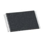
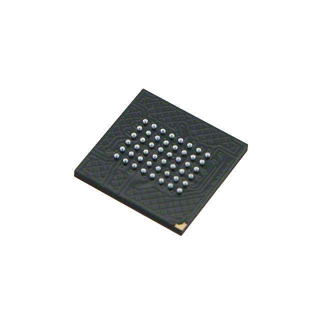
| 产品图片 |
|
| rohs | 符合RoHS无铅 / 符合限制有害物质指令(RoHS)规范要求 |
| 产品系列 | 内存,电可擦除可编程只读存储器,Atmel AT28C256F-15TU- |
| 数据手册 | |
| 产品型号 | AT28C256F-15TU |
| 产品目录页面 | |
| 产品种类 | 电可擦除可编程只读存储器 |
| 供应商器件封装 | 28-TSOP |
| 其它名称 | AT28C256F15TU |
| 包装 | 托盘 |
| 商标 | Atmel |
| 存储器类型 | EEPROM |
| 存储容量 | 256 kbit |
| 安装风格 | SMD/SMT |
| 封装/外壳 | 28-TSSOP (0.465", 11.80mm 宽) |
| 封装/箱体 | TSOP-28 |
| 工作温度 | -40°C ~ 85°C |
| 工作电流 | 50 mA |
| 工作电源电压 | 5 V |
| 工厂包装数量 | 234 |
| 接口 | 并联 |
| 接口类型 | SPI |
| 数据保留 | 10 yr |
| 最大工作温度 | + 85 C |
| 最大工作电流 | 50 mA |
| 最小工作温度 | - 40 C |
| 标准包装 | 234 |
| 格式-存储器 | EEPROMs - 并行 |
| 电压-电源 | 4.5 V ~ 5.5 V |
| 电源电压-最大 | 5.5 V |
| 电源电压-最小 | 4.5 V |
| 组织 | 32 k x 8 |
| 访问时间 | 150 ns |
| 输出启用访问时间 | 70 ns |
| 速度 | 150ns |


_renders/MR4A16BCYS35.jpg)


- 商务部:美国ITC正式对集成电路等产品启动337调查
- 曝三星4nm工艺存在良率问题 高通将骁龙8 Gen1或转产台积电
- 太阳诱电将投资9.5亿元在常州建新厂生产MLCC 预计2023年完工
- 英特尔发布欧洲新工厂建设计划 深化IDM 2.0 战略
- 台积电先进制程称霸业界 有大客户加持明年业绩稳了
- 达到5530亿美元!SIA预计今年全球半导体销售额将创下新高
- 英特尔拟将自动驾驶子公司Mobileye上市 估值或超500亿美元
- 三星加码芯片和SET,合并消费电子和移动部门,撤换高东真等 CEO
- 三星电子宣布重大人事变动 还合并消费电子和移动部门
- 海关总署:前11个月进口集成电路产品价值2.52万亿元 增长14.8%
_renders/IS42S32800D-6BLI.jpg)


PDF Datasheet 数据手册内容提取
Features (cid:129) FastReadAccessTime–150ns (cid:129) AutomaticPageWriteOperation – InternalAddressandDataLatchesfor64Bytes – InternalControlTimer (cid:129) FastWriteCycleTimes – PageWriteCycleTime:3msor10msMaximum – 1to64-bytePageWriteOperation (cid:129) LowPowerDissipation 256K (32K x 8) – 50mAActiveCurrent – 200 µACMOSStandbyCurrent Paged Parallel (cid:129) HardwareandSoftwareDataProtection (cid:129) DATAPollingforEndofWriteDetection EEPROM (cid:129) HighReliabilityCMOSTechnology – Endurance:104or105Cycles – DataRetention:10Years AT28C256 (cid:129) Single5V±10%Supply (cid:129) CMOSandTTLCompatibleInputsandOutputs (cid:129) JEDECApprovedByte-widePinout (cid:129) FullMilitaryandIndustrialTemperatureRanges (cid:129) Green(Pb/Halide-free)PackagingOption 1. Description The AT28C256 is a high-performance electrically erasable and programmable read- only memory. Its 256K of memory is organized as 32,768 words by 8 bits. Manufac- tured with Atmel’s advanced nonvolatile CMOS technology, the device offers access timesto150nswithpowerdissipationofjust440mW.Whenthedeviceisdeselected, theCMOSstandbycurrentislessthan200 µA. The AT28C256 is accessed like a Static RAM for the read or write cycle without the need for external components. The device contains a 64-byte page register to allow writing ofup to64 bytes simultaneously. During awrite cycle, theaddresses and1 to 64 bytes of data are internally latched, freeing the address and data bus for other operations. Following the initiation of a write cycle, the device will automatically write the latched data using an internal control timer. The end of a write cycle can be detectedbyDATAPollingofI/O7.Oncetheendofawritecyclehasbeendetecteda newaccessforareadorwritecanbegin. Atmel’s AT28C256 has additional featuresto ensure high qualityand manufacturabil- ity.Thedeviceutilizesinternalerrorcorrectionforextendedenduranceandimproved data retention characteristics. An optional software data protection mechanism is available to guard against inadvertent writes. The device also includes an extra 64bytesofEEPROMfordeviceidentificationortracking. 0006M–PEEPR–12/09
2. Pin Configurations PinName Function A0-A14 Addresses CE ChipEnable OE OutputEnable WE WriteEnable I/O0-I/O7 DataInputs/Outputs NC NoConnect DC Don’tConnect 2.1 28-lead TSOP Top View 2.3 32-pad LCC, 28-lead PLCC Top View OE 1 28 A10 A7 A12 A14 DC VCC WE A13 A11 2 27 CE 4 3 2 1 2 1 0 3 3 3 A9 3 26 I/O7 A6 5 29 A8 A8 4 25 I/O6 A5 6 28 A9 A13 5 24 I/O5 A4 7 27 A11 WE 6 23 I/O4 A3 8 26 NC VCC 7 22 I/O3 A2 9 25 OE A14 8 21 GND A1 10 24 A10 A12 9 20 I/O2 A0 11 23 CE A7 10 19 I/O1 NC 12 22 I/O7 A6 11 18 I/O0 I/O0 13 21 I/O6 4 5 6 7 8 9 0 A5 12 17 A0 1 1 1 1 1 1 2 A4 13 16 A1 1 2 D C 3 4 5 O O N D O O O A3 14 15 A2 I/ I/ G I/ I/ I/ Note: PLCCpackagepins1and17areDon’tConnect. 2.4 28-lead Cerdip/PDIP/Flatpack/SOIC – 2.2 28-lead PGA Top View Top View A14 1 28 VCC A12 2 27 WE A7 3 26 A13 A6 4 25 A8 A5 5 24 A9 A4 6 23 A11 A3 7 22 OE A2 8 21 A10 A1 9 20 CE A0 10 19 I/O7 I/O0 11 18 I/O6 I/O1 12 17 I/O5 I/O2 13 16 I/O4 GND 14 15 I/O3 AT28C256 2 0006M–PEEPR–12/09
AT28C256 3. Block Diagram 4. Device Operation 4.1 Read The AT28C256 is accessed like a Static RAM. When CE and OE are low and WE is high, the data stored at the memory location determined by the address pins is asserted on the outputs. The outputs are put in the high impedance state when either CE or OE is high. This dual-line controlgivesdesignersflexibilityinpreventingbuscontentionintheirsystem. 4.2 Byte Write AlowpulseontheWEorCEinputwithCEorWElow(respectively)andOEhighinitiatesawrite cycle.TheaddressislatchedonthefallingedgeofCEorWE,whicheveroccurslast.Thedatais latchedbythefirstrisingedgeofCEorWE.Onceabytewritehasbeenstarteditwillautomati- cally time itself to completion. Once a programming operation has been initiated and for the durationoft ,areadoperationwilleffectivelybeapollingoperation. WC 4.3 Page Write The page write operation of the AT28C256 allows 1 to 64 bytes of data to be written into the device during a single internal programming period. A page write operation is initiated in the same manner as a byte write; the first byte written can then be followed by 1 to 63 additional bytes.Eachsuccessivebytemustbewrittenwithin150 µs(t )ofthepreviousbyte.Ifthet BLC BLC limitisexceededtheAT28C256willceaseacceptingdataandcommencetheinternalprogram- ming operation. All bytes during a page write operation must reside on the same page as defined by the state of the A6 - A14 inputs. For each WE high to low transition during the page writeoperation,A6-A14mustbethesame. TheA0toA5inputsareusedtospecifywhichbyteswithinthepagearetobewritten.Thebytes may be loaded in any order and may be altered within the same load period. Only bytes which are specified for writing will be written; unnecessary cycling of other bytes within the page does notoccur. 4.4 DATA Polling TheAT28C256featuresDATAPollingtoindicatetheendofawritecycle.Duringabyteorpage write cycle an attempted read of the last byte written will result in the complement of the written datatobepresentedonI/O7.Oncethewritecyclehasbeencompleted,truedataisvalidonall outputs,andthenextwritecyclemaybegin.DATAPollingmaybeginatanytimeduringthewrite cycle. 3 0006M–PEEPR–12/09
4.5 Toggle Bit InadditiontoDATAPollingtheAT28C256providesanothermethodfordeterminingtheendofa write cycle. During the write operation, successive attempts to read data from the device will result in I/O6 toggling between one and zero. Once the write has completed, I/O6 will stop tog- gling and valid data will be read. Reading the toggle bit may begin at any time during the write cycle. 4.6 Data Protection If precautions are not taken, inadvertent writes may occur during transitions of the host system power supply. Atmel has incorporated both hardware and software features that will protect the memoryagainstinadvertentwrites. 4.6.1 HardwareProtection HardwarefeaturesprotectagainstinadvertentwritestotheAT28C256inthefollowingways:(a) V sense–ifV isbelow3.8V(typical)thewritefunctionisinhibited;(b)V power-ondelay– CC CC CC once V has reached 3.8V the device will automatically time out 5 ms (typical) before allowing CC a write; (c) write inhibit – holding any one of OE low, CE high or WE high inhibits write cycles; and(d)noisefilter–pulsesoflessthan15ns(typical)ontheWEorCEinputswillnotinitiatea writecycle. 4.6.2 SoftwareDataProtection A software controlled data protection feature has been implemented on the AT28C256. When enabled, the software data protection (SDP), will prevent inadvertent writes. The SDP feature may be enabled or disabled by the user; the AT28C256 is shipped from Atmel with SDP disabled. SDP is enabled by the host system issuing a series of three write commands; three specific bytes of data are written to three specific addresses (refer to “Software Data Protection” algo- rithm). After writing the 3-byte command sequence and after t the entire AT28C256 will be WC protected against inadvertent write operations. It should be noted, that once protected the host maystillperformabyteorpagewritetotheAT28C256.Thisisdonebyprecedingthedatatobe writtenbythesame3-bytecommandsequenceusedtoenableSDP. Onceset,SDPwillremainactiveunlessthedisablecommandsequenceisissued.Powertransi- tionsdonotdisableSDPandSDPwillprotecttheAT28C256duringpower-upandpower-down conditions. All command sequences must conform to the page write timing specifications. The dataintheenableanddisablecommandsequencesisnotwrittentothedeviceandthememory addresses used in the sequence may be written with data in either a byte or page write operation. AftersettingSDP,anyattempttowritetothedevicewithoutthe3-bytecommandsequencewill start the internal write timers. No data will be written to the device; however, for the duration of t ,readoperationswilleffectivelybepollingoperations. WC 4.7 Device Identification Anextra64bytesofEEPROMmemoryareavailabletotheuserfordeviceidentification.Byrais- ingA9to12V±0.5Vandusingaddresslocations7FC0Hto7FFFHtheadditionalbytesmaybe writtentoorreadfrominthesamemannerastheregularmemoryarray. 4.8 Optional Chip Erase Mode The entire device can be erased using a 6-byte software code. Please see “Software Chip Erase”applicationnotefordetails. AT28C256 4 0006M–PEEPR–12/09
AT28C256 5. DC and AC Operating Range AT28C256-15 AT28C256-20 AT28C256-25 AT28C256-35 OperatingTemperature Ind. -40°C-85°C (Case) Mil. -55°C-125°C -55°C-125°C -55°C-125°C -55°C-125°C V PowerSupply 5V ±10% 5V ±10% 5V ±10% 5V ±10% CC 6. Operating Modes Mode CE OE WE I/O Read V V V D IL IL IH OUT Write(2) V V V D IL IH IL IN Standby/WriteInhibit V X(1) X HighZ IH WriteInhibit X X V IH WriteInhibit X V X IL OutputDisable X V X HighZ IH ChipErase V V (3) V HighZ IL H IL Notes: 1. XcanbeV orV . IL IH 2. RefertoACprogrammingwaveforms. 3. V =12.0V±0.5V. H 7. Absolute Maximum Ratings* TemperatureunderBias................................-55°Cto+125°C *NOTICE: Stressesbeyondthoselistedunder“Absolute MaximumRatings”maycausepermanentdam- StorageTemperature.....................................-65°Cto+150°C agetothedevice.Thisisastressratingonlyand functionaloperationofthedeviceattheseorany AllInputVoltages otherconditionsbeyondthoseindicatedinthe (includingNCPins) operationalsectionsofthisspecificationisnot withRespecttoGround...................................-0.6Vto+6.25V implied.Exposuretoabsolutemaximumrating conditionsforextendedperiodsmayaffect AllOutputVoltages devicereliability withRespecttoGround.............................-0.6VtoV +0.6V CC VoltageonOEandA9 withRespecttoGround...................................-0.6Vto+13.5V 8. DC Characteristics Symbol Parameter Condition Min Max Units I InputLoadCurrent V =0VtoV +1V 10 µA LI IN CC I OutputLeakageCurrent V =0VtoV 10 µA LO I/O CC Ind. 200 µA I V StandbyCurrentCMOS CE=V -0.3VtoV +1V SB1 CC CC CC Mil. 300 µA I V StandbyCurrentTTL CE=2.0VtoV +1V 3 mA SB2 CC CC I V ActiveCurrent f=5MHz;I =0mA 50 mA CC CC OUT V InputLowVoltage 0.8 V IL V InputHighVoltage 2.0 V IH V OutputLowVoltage I =2.1mA 0.45 V OL OL V OutputHighVoltage I =-400 µA 2.4 V OH OH 5 0006M–PEEPR–12/09
9. AC Read Characteristics AT28C256-15 AT28C256-20 AT28C256-25 AT28C256-35 Symbol Parameter Min Max Min Max Min Max Min Max Units t AddresstoOutputDelay 150 200 250 350 ns ACC t (1) CEtoOutputDelay 150 200 250 350 ns CE t (2) OEtoOutputDelay 0 70 0 80 0 100 0 100 ns OE t (3)(4) CEorOEtoOutputFloat 0 50 0 55 0 60 0 70 ns DF OutputHoldfromOE,CEor t 0 0 0 0 ns OH Address,whicheveroccurredfirst 10. AC Read Waveforms(1)(2)(3)(4) Notes: 1. CEmaybedelayeduptot -t aftertheaddresstransitionwithoutimpactont . ACC CE ACC 2. OEmaybedelayeduptot -t afterthefallingedgeofCEwithoutimpactont orbyt -t afteranaddresschange CE OE CE ACC OE withoutimpactont . ACC 3. t isspecifiedfromOEorCEwhicheveroccursfirst(C =5pF). DF L 4. Thisparameterischaracterizedandisnot100%tested. AT28C256 6 0006M–PEEPR–12/09
AT28C256 11. Input Test Waveforms and Measurement Level t ,t <5ns R F 12. Output Test Load 13. Pin Capacitance f=1MHz,T=25°C(1) Symbol Typ Max Units Conditions C 4 6 pF V =0V IN IN C 8 12 pF V =0V OUT OUT Note: 1. Thisparameterischaracterizedandisnot100%tested. 7 0006M–PEEPR–12/09
14. AC Write Characteristics Symbol Parameter Min Max Units t ,t Address,OESetupTime 0 ns AS OES t AddressHoldTime 50 ns AH t ChipSelectSetupTime 0 ns CS t ChipSelectHoldTime 0 ns CH t WritePulseWidth(WEorCE) 100 ns WP t DataSetupTime 50 ns DS t ,t Data,OEHoldTime 0 ns DH OEH t TimetoDataValid NR(1) DV Note: 1. NR=NoRestriction 15. AC Write Waveforms 15.1 WE Controlled 15.2 CE Controlled AT28C256 8 0006M–PEEPR–12/09
AT28C256 16. Page Mode Characteristics Symbol Parameter Min Max Units AT28C256 10 ms t WriteCycleTime(optionavailable) WC AT28C256F 3 ms t AddressSetupTime 0 ns AS t AddressHoldTime 50 ns AH t DataSetupTime 50 ns DS t DataHoldTime 0 ns DH t WritePulseWidth 100 ns WP t ByteLoadCycleTime 150 µs BLC t WritePulseWidthHigh 50 ns WPH 17. Page Mode Write Waveforms(1)(2) Notes: 1. A6throughA14mustspecifythesamepageaddressduringeachhightolowtransitionofWE(orCE). 2. OEmustbehighonlywhenWEandCEarebothlow. 18. Chip Erase Waveforms t =t =5µsec(min.) S H t =10msec(min.) W V =12.0V±0.5V H 9 0006M–PEEPR–12/09
19. Software Data Protection 20. Software Data Protection Enable Algorithm(1) Disable Algorithm(1) LOADDATAAA LOADDATAAA TO TO ADDRESS5555 ADDRESS5555 LOADDATA55 LOADDATA55 TO TO ADDRESS2AAA ADDRESS2AAA LOADDATAA0 LOADDATA80 TO TO ADDRESS5555 ADDRESS5555 WRITESENABLED(2) LOADDATAXX LOADDATAAA TO TO ANYADDRESS(4) ADDRESS5555 LOADLASTBYTE LOADDATA55 TO TO LASTADDRESS ADDRESS2AAA ENTERDATA PROTECTSTATE LOADDATA20 Notes: 1. DataFormat:I/O7-I/O0(Hex); TO AddressFormat:A14-A0(Hex). ADDRESS5555 EXITDATA 2. WriteProtectstatewillbeactivatedatendofwrite PROTECTSTATE(3) evenifnootherdataisloaded. LOADDATAXX 3. WriteProtectstatewillbedeactivatedatendofwrite TO periodevenifnootherdataisloaded. ANYADDRESS(4) 4. 1to64bytesofdataareloaded. LOADLASTBYTE TO LASTADDRESS 21. Software Protected Write Cycle Waveforms(1)(2) Notes: 1. A6throughA14mustspecifythesamepageaddressduringeachhightolowtransitionofWE(orCE)afterthesoftware codehasbeenentered. 2. OEmustbehighonlywhenWEandCEarebothlow. AT28C256 10 0006M–PEEPR–12/09
AT28C256 22. Data Polling Characteristics(1) Symbol Parameter Min Typ Max Units t DataHoldTime 0 ns DH t OEHoldTime 0 ns OEH t OEtoOutputDelay(2) ns OE t WriteRecoveryTime 0 ns WR Notes: 1. Theseparametersarecharacterizedandnot100%tested. 2. See“ACReadCharacteristics”onpage6. 23. Data Polling Waveforms 24. Toggle Bit Characteristics(1) Symbol Parameter Min Typ Max Units t DataHoldTime 10 ns DH t OEHoldTime 10 ns OEH t OEtoOutputDelay(2) ns OE t OEHighPulse 150 ns OEHP t WriteRecoveryTime 0 ns WR Notes: 1. Theseparametersarecharacterizedandnot100%tested. 2. See“ACReadCharacteristics”onpage6. 25. Toggle Bit Waveforms(1)(2)(3) Notes: 1. TogglingeitherOEorCEorbothOEandCEwilloperatetogglebit. 2. BeginningandendingstateofI/O6willvary. 3. Anyaddresslocationmaybeusedbuttheaddressshouldnotvary. 11 0006M–PEEPR–12/09
26. Normalized I Graphs CC AT28C256 12 0006M–PEEPR–12/09
AT28C256 27. Ordering Information 27.1 27.1Military Dual Marked Package 27.1.1 AT28C256 t I (mA) ACC CC (ns) Active Standby OrderingCode Package OperationRange 150 50 0.3 AT28C256-15DM/883 5962-8852514XX(1) 28D6 5962-8852506XX AT28C256-15FM/883 5962-8852514ZX(1) 28F Military/883C 5962-8852506ZX ClassB,FullyCompliant AT28C256-15LM/883 (-55°Cto125°C) 5962-8852514YX(1) 32L 5962-8852506YX AT28C256-15UM/883 5962-8852514UX(1) 28U 5962-8852506UX 200 50 0.3 AT28C256-20DM/883 5962-8852512XX(1) 28D6 5962-8852504XX AT28C256-20FM/883 5962-8852512ZX(1) 28F Military/883C 5962-8852504ZX ClassB,FullyCompliant AT28C256-20LM/883 (-55°Cto125°C) 5962-8852512YX(1) 32L 5962-8852504YX AT28C256-20UM/883 5962-8852512UX(1) 28U 5962-8852504UX 250 50 0.3 AT28C256-25DM/883 5962-8852511XX(1) 28D6 5962-8852503XX AT28C256-25FM/883 5962-8852511ZX(1) 28F Military/883C 5962-8852503ZX ClassB,FullyCompliant AT28C256-25LM/883 (-55°Cto125°C) 5962-8852511YX(1) 32L 5962-8852503YX AT28C256-25UM/883 5962-8852511UX(1) 28U 5962-8852503UX Note: 1. WheretwoDESCnumbersapplytotheAtmelorderingcodeapplySL815toreceivepartswiththenotedDESCnumberdual markedalongwithAtmelpartnumber. 13 0006M–PEEPR–12/09
27.1.2 AT28C256E t I (mA) ACC CC (ns) Active Standby OrderingCode Package OperationRange 150 50 0.3 AT28C256E-15DM/883 5962-8852516XX(1) 28D6 5962-8852508XX AT28C256E-15FM/883 5962-8852516ZX(1) 28F Military/883C 5962-8852508ZX ClassB,FullyCompliant AT28C256E-15LM/883 (-55°Cto125°C) 5962-8852516YX(1) 32L 5962-8852508YX AT28C256E-15UM/883 5962-8852516UX(1) 28U 5962-8852508UX 200 50 0.3 AT28C256E-20DM/883 28D6 Military/883C AT28C256E-20FM/883 28F ClassB,FullyCompliant AT28C256E-20LM/883 32L (-55°Cto125°C) AT28C256E-20UM/883 28U 250 50 0.3 AT28C256E-25DM/883 5962-8852513XX(1) 28D6 5962-8852505XX 5962-8852505XX 5962-8852513ZX(1) 28F Military/883C 5962-8852505ZX ClassB,FullyCompliant AT28C256E-25LM/883 (-55°Cto125°C) 5962-8852513YX(1) 32L 5962-8852505YX AT28C256E-25UM/883 5962-8852513UX(1) 28U 5962-8852505UX Note: 1. WheretwoDESCnumbersapplytotheAtmelorderingcodeapplySL815toreceivepartswiththenotedDESCnumberdual markedalongwithAtmelpartnumber. AT28C256 14 0006M–PEEPR–12/09
AT28C256 27.1.3 AT28C256F t I (mA) ACC CC (ns) Active Standby OrderingCode Package OperationRange 150 50 0.3 AT28C256F-15DM/883 5962-8852515XX(3) 28D6 5962-8852507XX AT28C256F-15FM/883 5962-8852515ZX(3) 28F Military/883C 5962-8852507ZX ClassB,FullyCompliant AT28C256F-15LM/883 (-55°Cto125°C) 5962-8852515YX(3) 32L 5962-8852507YX AT28C256F-15UM/883 5962-8852515UX(3) 28U 5962-8852507UX Notes: 1. ElectricalspecificationsforthesespeedsaredefinedbyStandardMicrocircuitDrawing5962-88525. 2. SMDspecifiesSoftwareDataProtectionfeaturefordevicetype,althoughAtmelproductsuppliedtoeverydevicetypeinthe SMDis100%testedforthisfeature. 3. WheretwoDESCnumbersapplytotheAtmelorderingcodeapplySL815toreceivepartswiththenotedDESCnumberdual markedalongwithAtmelpartnumber. PackageType 28D6 28-lead,0.600"Wide,Non-windowed,CeramicDualInlinePackage(Cerdip) 28F 28-lead,Non-windowed,CeramicBottom-brazedFlatPackage(Flatpack) 32L 32-pad,Non-windowed,CeramicLeadlessChipCarrier(LCC) 28U 28-pin,CeramicPinGridArray(PGA) W Die Options Blank StandardDevice:Endurance=10KWriteCycles;WriteTime=10ms E HighEnduranceOption:Endurance=100KWriteCycles F FastWriteOption:WriteTime=3ms 15 0006M–PEEPR–12/09
27.2 Industrial Green Package Option (Pb/Halide-free) 27.2.1 AT28C256 t I (mA) ACC CC (ns) Active Standby OrderingCode Package OperationRange 150 50 0.2 AT28C256-15JU 32J AT28C256-15PU 28P6 Industrial AT28C256-15SU 28S (-40°Cto85°C) AT28C256-15TU 28T 27.2.2 AT28C256E t I (mA) ACC CC (ns) Active Standby OrderingCode Package OperationRange 150 50 0.2 AT28C256E-15JU 32J Industrial AT28C256E-15SU 28S (-40°Cto85°C) AT28C256E-15TU 28T 27.2.3 AT28C256F t I (mA) ACC CC (ns) Active Standby OrderingCode Package OperationRange 150 50 0.2 AT28C256F-15JU 32J Industrial AT28C256F-15SU 28S (-40°Cto85°C) AT28C256F-15TU 28T PackageType 32J 32-lead,PlasticJ-leadedChipCarrier(PLCC) 28P6 28-lead,0.600"Wide,PlasticDualInlinePackage(PDIP) 28S 28-lead,0.300"Wide,PlasticGullWingSmallOutline(SOIC) 28T 28-lead,PlasticThinSmallOutlinePackage(TSOP) Options Blank StandardDevice:Endurance=10KWriteCycles;WriteTime=10ms E HighEnduranceOption:Endurance=100KWriteCycles F FastWriteOption:WriteTime=3ms 28. Die Products ReferenceSection:ContactAtmelsalesfordiesalesoptions. AT28C256 16 0006M–PEEPR–12/09
AT28C256 29. Packaging Information 29.1 28D6 – Cerdip Dimensions in Millimeters and (Inches). Controlling dimension: Inches. MIL-STD 1835 D-10 Config A (Glass Sealed) 37.85(1.490) 36.58(1.440) PIN 1 15.49(0.610) 12.95(0.510) 33.02(1.300) REF 5.72(0.225) 0.127(0.005)MIN MAX SEATING PLANE 1.52(0.060) 5.08(0.200) 0.38(0.015) 3.18(0.125) 0.66(0.026) 1.65(0.065) 0.36(0.014) 2.54(0.100)BSC 1.14(0.045) 15.70(0.620) 15.00(0.590) 0.46(0.018) 0º~ 15º REF 0.20(0.008) 17.80(0.700) MAX 10/23/03 TITLE DRAWING NO. REV. 2325 Orchard Parkway 28D6, 28-lead, 0.600" Wide, Non-windowed, San Jose, CA 95131 28D6 B R Ceramic Dual Inline Package (Cerdip) 17 0006M–PEEPR–12/09
29.2 28F – Flatpack Dimensions in Millimeters and (Inches). Controlling dimension: Inches. MIL-STD 1835 F-12 Config B 9.40(0.370) PIN #1 ID 6.35(0.250) 0.56(0.022) 0.38(0.015) 1.27(0.050) BSC 18.49(0.728) 18.08(0.712) 1.14(0.045) MAX 10.57(0.416) 9.75(0.384) 0.23(0.009) 3.02(0.119) 0.10(0.004) 2.29(0.090) 1.96(0.077) 1.09(0.043) 1.14(0.045) 7.26(0.286) 0.660(0.026) 6.96(0.274) 10/21/03 TITLE DRAWING NO. REV. 2325 Orchard Parkway 28F, 28-lead, Non-windowed, Ceramic Bottom-brazed San Jose, CA 95131 28F B R Flat Package (FlatPack) AT28C256 18 0006M–PEEPR–12/09
AT28C256 29.3 32J – PLCC 1.14(0.045)X45 PINNO.1 1.14(0.045)X45 IDENTIFIER 0.318(0.0125) 0.191(0.0075) E1 E B1 E2 B e A2 D1 A1 D A 0.51(0.020)MAX 45 MAX(3X) COMMONDIMENSIONS (UnitofMeasure=mm) SYMBOL MIN NOM MAX NOTE D2 A 3.175 – 3.556 A1 1.524 – 2.413 A2 0.381 – – D 12.319 – 12.573 D1 11.354 – 11.506 Note2 D2 9.906 – 10.922 Notes: 1.ThispackageconformstoJEDECreferenceMS-016,VariationAE. E 14.859 – 15.113 2.DimensionsD1andE1donotincludemoldprotrusion. Allowableprotrusionis.010"(0.254mm)perside.DimensionD1 E1 13.894 – 14.046 Note2 andE1includemoldmismatchandaremeasuredattheextreme E2 12.471 – 13.487 materialconditionattheupperorlowerpartingline. B 0.660 – 0.813 3.Leadcoplanarityis0.004"(0.102mm)maximum. B1 0.330 – 0.533 e 1.270TYP 10/04/01 TITLE DRAWINGNO. REV. 2325OrchardParkway 32J,32-lead,PlasticJ-leadedChipCarrier(PLCC) SanJose,CA 95131 32J B R 19 0006M–PEEPR–12/09
29.4 32L – LCC Dimensions in Millimeters and (Inches). Controlling dimension: Inches. MIL-STD 1835 C-12 11.63(0.458) 11.23(0.442) 2.54(0.100) 2.16(0.085) 14.22(0.560) 13.72(0.540) 1.91(0.075) 1.40(0.055) PIN 1 1.40(0.055) 2.41(0.095) 1.14(0.045) INDEX CORNER 1.91(0.075) 0.635(0.025) X 45˚ 0.381(0.015) 0.305(0.012) RADIUS 0.178(0.007) 10.16(0.400) BSC 0.737(0.029) 0.533(0.021) 1.27(0.050) TYP 1.02(0.040) X 45˚ 2.16(0.085) 7.62(0.300) BSC 1.65(0.065) 10/21/03 TITLE DRAWING NO. REV. 2325 Orchard Parkway 32L, 32-pad, Non-windowed, Ceramic Lid, Leadless Chip San Jose, CA 95131 32L B R Carrier (LCC) AT28C256 20 0006M–PEEPR–12/09
AT28C256 29.5 28P6 – PDIP D PIN 1 E1 A SEATING PLANE A1 L B B1 e E COMMON DIMENSIONS 0º ~ 15º REF (Unit of Measure = mm) C SYMBOL MIN NOM MAX NOTE eB A – – 4.826 A1 0.381 – – D 36.703 – 37.338 Note 2 E 15.240 – 15.875 E1 13.462 – 13.970 Note 2 B 0.356 – 0.559 B1 1.041 – 1.651 Notes: 1.This package conforms to JEDEC reference MS-011, Variation AB. 2.Dimensions D and E1 do not include mold Flash or Protrusion. L 3.048 – 3.556 Mold Flash or Protrusion shall not exceed 0.25 mm (0.010"). C 0.203 – 0.381 eB 15.494 – 17.526 e 2.540 TYP 09/28/01 TITLE DRAWING NO. REV. 2325 Orchard Parkway 28P6, 28-lead (0.600"/15.24 mm Wide) Plastic Dual R San Jose, CA 95131 Inline Package (PDIP) 28P6 B 21 0006M–PEEPR–12/09
29.6 28S – SOIC Dimensions in Millimeters and (Inches). Controlling dimension: Millimeters. 0.51(0.020) 0.33(0.013) 7.60(0.2992) 10.65(0.419) 7.40(0.2914) 10.00(0.394) PIN 1 1.27(0.50) BSC TOP VIEW 18.10(0.7125) 2.65(0.1043) 17.70(0.6969) 2.35(0.0926) 0.30(0.0118) 0.10(0.0040) SIDE VIEWS 0º ~ 8º 0.32(0.0125) 0.23(0.0091) 1.27(0.050) 0.40(0.016) 8/4/03 TITLE DRAWING NO. REV. 2325 Orchard Parkway 28S, 28-lead, 0.300" Body, Plastic Gull Wing Small Outline (SOIC) San Jose, CA 95131 28S B R JEDEC Standard MS-013 AT28C256 22 0006M–PEEPR–12/09
AT28C256 29.7 28T – TSOP PIN 1 0º ~ 5º c Pin 1 Identifier Area D1 D L e b L1 E A2 A SEATING PLANE GAGE PLANE COMMON DIMENSIONS A1 (Unit of Measure = mm) SYMBOL MIN NOM MAX NOTE A – – 1.20 A1 0.05 – 0.15 A2 0.90 1.00 1.05 Notes: 1.This package conforms to JEDEC reference MO-183. D 13.20 13.40 13.60 2.Dimensions D1 and E do not include mold protrusion. Allowable D1 11.70 11.80 11.90 Note 2 protrusion on E is 0.15 mm per side and on D1 is 0.25 mm per side. 3. Lead coplanarity is 0.10 mm maximum. E 7.90 8.00 8.10 Note 2 L 0.50 0.60 0.70 L1 0.25 BASIC b 0.17 0.22 0.27 c 0.10 – 0.21 e 0.55 BASIC 12/06/02 TITLE DRAWING NO. REV. 2325 Orchard Parkway 28T, 28-lead (8 x 13.4 mm) Plastic Thin Small Outline San Jose, CA 95131 28T C R Package, Type I (TSOP) 23 0006M–PEEPR–12/09
29.8 28U – PGA Dimensions in Millimeters and (Inches). Controlling dimension: Inches. 7.26(0.286) 6.50(0.256) 13.74(0.540) 2.57(0.101) 13.36(0.526) 2.06(0.081) 1.40(0.055) 1.14(0.045) 0.58(0.023) 15.24(0.600) 0.43(0.017) 14.88(0.586) 3.12(0.123) 2.62(0.103) 1.83(0.072) 1.57(0.062) 14.17(0.558) 13.77(0.542) 2.54(0.100) TYP 16.71(0.658) 12.70(0.500) TYP 16.31(0.642) 2.54(0.100) TYP 10.41(0.410) 9.91(0.390) 10/21/03 TITLE DRAWING NO. REV. 2325 Orchard Parkway 28U, 28-pin, Ceramic Pin Grid Array (PGA) San Jose, CA 95131 28U B R AT28C256 24 0006M–PEEPR–12/09
Headquarters International AtmelCorporation AtmelAsia AtmelEurope AtmelJapan 2325OrchardParkway Unit1-5&16,19/F LeKrebs 9F,TonetsuShinkawaBldg. SanJose,CA95131 BEATower,MillenniumCity5 8,RueJean-PierreTimbaud 1-24-8Shinkawa USA 418KwunTongRoad BP309 Chuo-ku,Tokyo104-0033 Tel:1(408)441-0311 KwunTong,Kowloon 78054Saint-Quentin-en- Japan Fax:1(408)487-2600 HongKong YvelinesCedex Tel:(81)3-3523-3551 Tel:(852)2245-6100 France Fax:(81)3-3523-7581 Fax:(852)2722-1369 Tel:(33)1-30-60-70-00 Fax:(33)1-30-60-71-11 Product Contact WebSite TechnicalSupport SalesContact www.atmel.com p_eeprom@atmel.com www.atmel.com/contacts LiteratureRequests www.atmel.com/literature Disclaimer: The information in this document is provided in connection with Atmel products. No license, express or implied, by estoppel or otherwise,to any intellectualpropertyrightisgrantedbythisdocumentorinconnectionwiththesaleofAtmelproducts.EXCEPTASSETFORTHINATMEL’STERMSANDCONDI- TIONSOFSALELOCATEDONATMEL’SWEBSITE,ATMELASSUMESNOLIABILITYWHATSOEVERANDDISCLAIMSANYEXPRESS,IMPLIEDORSTATUTORY WARRANTYRELATINGTOITSPRODUCTSINCLUDING,BUTNOTLIMITEDTO,THEIMPLIEDWARRANTYOFMERCHANTABILITY,FITNESSFORAPARTICULAR PURPOSE,ORNON-INFRINGEMENT.INNOEVENTSHALLATMELBELIABLEFORANYDIRECT,INDIRECT,CONSEQUENTIAL,PUNITIVE,SPECIALORINCIDEN- TALDAMAGES(INCLUDING,WITHOUTLIMITATION,DAMAGESFORLOSSOFPROFITS,BUSINESSINTERRUPTION,ORLOSSOFINFORMATION)ARISINGOUTOF THE USE OR INABILITY TO USE THIS DOCUMENT, EVEN IF ATMEL HAS BEEN ADVISED OF THE POSSIBILITY OF SUCH DAMAGES. Atmel makes no representationsorwarrantieswithrespecttotheaccuracyorcompletenessofthecontentsofthisdocumentandreservestherighttomakechangestospecifications andproductdescriptionsatanytimewithoutnotice.Atmeldoesnotmakeanycommitmenttoupdatetheinformationcontainedherein.Unlessspecificallyprovided otherwise,Atmelproductsarenotsuitablefor,andshallnotbeusedin,automotiveapplications.Atmel’sproductsarenotintended,authorized,orwarrantedforuse ascomponentsinapplicationsintendedtosupportorsustainlife. ©2009AtmelCorporation.Allrightsreserved. Atmel®, Atmel logo and combinations thereof, and others are registered trademarks or trade- marksofAtmelCorporationoritssubsidiaries.Othertermsandproductnamesmaybetrademarksofothers. 0006M–PEEPR–12/09
Mouser Electronics Authorized Distributor Click to View Pricing, Inventory, Delivery & Lifecycle Information: M icrochip: AT28C256-15SI AT28C256-15SC AT28C256-20PC AT28C256-25DM/883 AT28C256-20JI AT28C256E-15PC AT28C256E-15JC AT28C256E-15TC AT28C256E-15SC AT28C256E-15JI AT28C256-15UM/883 AT28C256E-20JC AT28C256E-20JI AT28C256-25PC AT28C256-25JI AT28C256-25TC AT28C256-25JC AT28C256-15TC AT28C256F-15PC AT28C256-15PI AT28C256-15JC AT28C256-15JI AT28C256-15PC AT28C256E-25JC AT28C256E-15DM/883 AT28C256-25SC AT28C256-25SI AT28C256-25TI AT28C256E-15JU AT28C256E-15PU AT28C256E-15SU AT28C256E-15TU AT28C256EF-15JU AT28C256-15DM/883 AT28C256-15FM/883 AT28C256- 15JU AT28C256-15LM/883 AT28C256-15PU AT28C256-15SU AT28C256-15TI AT28C256-15TU AT28C256- 20DM/883 AT28C256-20FM/883 AT28C256-20JC AT28C256-20LM/883 AT28C256-20PI AT28C256-20SC AT28C256-20SI AT28C256-20TC AT28C256-20TI AT28C256-20UM/883 AT28C256-25FM/883 AT28C256- 25LM/883 AT28C256-25PI AT28C256-25UM/883 AT28C256E-15FM/883 AT28C256E-15LM/883 AT28C256E-15PI AT28C256E-15SI AT28C256E-15TI AT28C256E-15UM/883 AT28C256E-20DM/883 AT28C256E-20FM/883 AT28C256E-20LM/883 AT28C256E-20PC AT28C256E-20PI AT28C256E-20SI AT28C256E-20TI AT28C256E- 20UM/883 AT28C256E-25DM/883 AT28C256E-25FM/883 AT28C256E-25JI AT28C256E-25LM/883 AT28C256E- 25PC AT28C256E-25PI AT28C256E-25UM/883 AT28C256F-15DM/883 AT28C256F-15FM/883 AT28C256F-15JC AT28C256F-15JI AT28C256F-15JU AT28C256F-15LM/883 AT28C256F-15PI AT28C256F-15PU AT28C256F-15SC AT28C256F-15SI AT28C256F-15SU AT28C256F-15TC AT28C256F-15TI AT28C256F-15TU AT28C256F- 15UM/883 AT28C256F-20DM/883 AT28C256F-20FM/883 AT28C256F-20JC AT28C256F-20JI AT28C256F- 20LM/883 AT28C256F-20PC AT28C256F-20PI AT28C256F-20SC AT28C256F-20SI