ICGOO在线商城 > 集成电路(IC) > PMIC - 显示器驱动器 > AS1100WL-T
 Datasheet下载
- 型号: AS1100WL-T
- 制造商: AUSTRIAMICROSYSTEMS
- 库位|库存: xxxx|xxxx
- 要求:
| 数量阶梯 | 香港交货 | 国内含税 |
| +xxxx | $xxxx | ¥xxxx |
查看当月历史价格
查看今年历史价格
AS1100WL-T产品简介:
ICGOO电子元器件商城为您提供AS1100WL-T由AUSTRIAMICROSYSTEMS设计生产,在icgoo商城现货销售,并且可以通过原厂、代理商等渠道进行代购。 AS1100WL-T价格参考。AUSTRIAMICROSYSTEMSAS1100WL-T封装/规格:PMIC - 显示器驱动器, 。您可以下载AS1100WL-T参考资料、Datasheet数据手册功能说明书,资料中有AS1100WL-T 详细功能的应用电路图电压和使用方法及教程。
AS1100WL-T是由ams(艾迈斯半导体)生产的一款PMIC(电源管理集成电路),专为显示器驱动器应用设计。其主要应用场景包括以下几方面:

1. 便携式消费电子设备:AS1100WL-T广泛应用于智能手机、平板电脑和可穿戴设备中的显示屏供电管理。它能够提供稳定的电压输出,支持低功耗模式,从而延长电池续航时间。

2. 中小型液晶显示屏:适用于导航仪、数码相机、便携式媒体播放器等设备中的LCD屏驱动。该芯片可以高效地调节电流和电压,确保显示屏亮度均匀且色彩鲜艳。

3. 汽车电子系统:在车载信息娱乐系统中,如仪表盘显示、后视镜摄像头画面显示等场景下使用。它具备良好的抗干扰能力和环境适应性,能够在宽温度范围内稳定工作。

4. 工业控制与医疗设备:例如患者监护仪、超声波机器上的触摸屏或图形界面显示部分。由于其高可靠性和精确的电源管理能力,非常适合需要长时间连续运行的场合。

5. 智能家居产品:如智能音箱、家庭自动化控制器等带屏幕显示功能的产品也可采用此款PMIC来优化显示效果并降低能耗。

总之,AS1100WL-T凭借其卓越的性能表现,在众多需要高质量显示效果同时又注重节能效率的应用领域中发挥着重要作用。
| 参数 | 数值 |
| 产品目录 | 集成电路 (IC) |
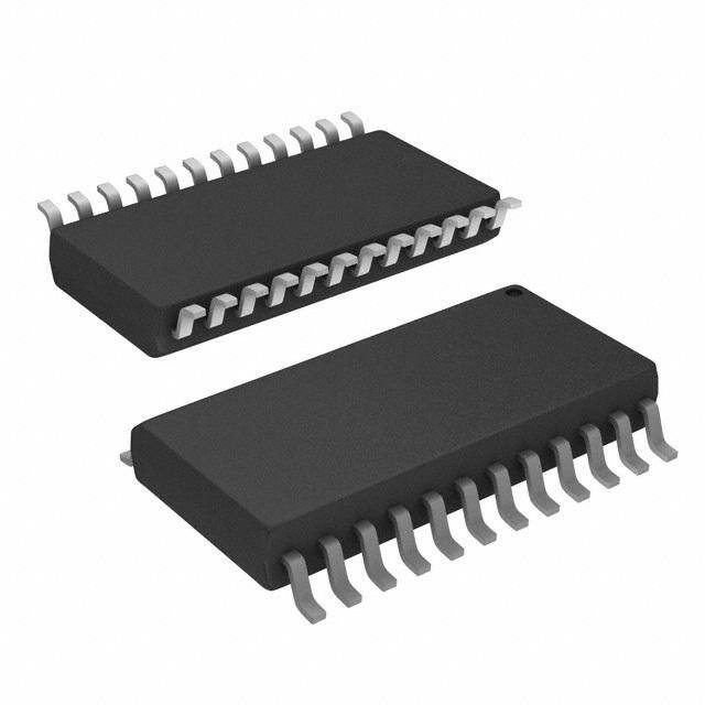
| 描述 | IC LED 8-DIGIT DRIVER 24-SOIC |
| 产品分类 | |
| 品牌 | ams |
| 数据手册 | http://www.ams.com/eng/content/download/1191/6932 |
| 产品图片 |
|
| 产品型号 | AS1100WL-T |
| rohs | 无铅 / 符合限制有害物质指令(RoHS)规范要求 |
| 产品系列 | - |
| 产品目录页面 | |
| 供应商器件封装 | 24-SOIC |
| 其它名称 | AS1100WL-TTR |
| 包装 | 带卷 (TR) |
| 安装类型 | 表面贴装 |
| 封装/外壳 | 24-SOIC(0.295",7.50mm 宽) |
| 工作温度 | 0°C ~ 70°C |
| 接口 | 串行 |
| 数字或字符 | 8 位数字 |
| 显示类型 | LED |
| 标准包装 | 1,500 |
| 电压-电源 | 4 V ~ 5.5 V |
| 电流-电源 | 330mA |
| 配置 | 7 段 + DP |


- 商务部:美国ITC正式对集成电路等产品启动337调查
- 曝三星4nm工艺存在良率问题 高通将骁龙8 Gen1或转产台积电
- 太阳诱电将投资9.5亿元在常州建新厂生产MLCC 预计2023年完工
- 英特尔发布欧洲新工厂建设计划 深化IDM 2.0 战略
- 台积电先进制程称霸业界 有大客户加持明年业绩稳了
- 达到5530亿美元!SIA预计今年全球半导体销售额将创下新高
- 英特尔拟将自动驾驶子公司Mobileye上市 估值或超500亿美元
- 三星加码芯片和SET,合并消费电子和移动部门,撤换高东真等 CEO
- 三星电子宣布重大人事变动 还合并消费电子和移动部门
- 海关总署:前11个月进口集成电路产品价值2.52万亿元 增长14.8%


PDF Datasheet 数据手册内容提取
austriamicrosystems AG is now ams AG The technical content of this austriamicrosystems datasheet is still valid. Contact information: Headquarters: ams AG Tobelbaderstrasse 30 8141 Unterpremstaetten, Austria Tel: +43 (0) 3136 500 0 e-Mail: ams_sales@ams.com Please visit our website at www.ams.com
Datasheet AS1100 Serially Interfaced, 8-Digit LED Driver 1 General Description 2 Key Features d The AS1100 is an LED driver for 7 segment numeric displays of up to (cid:1) 10MHz Serial Interface 8 digits. The AS1100 can be programmed via a conventional 4 wire (cid:1) Individual LED Segment Control serial interface. i (cid:1) Decode/No-Decode Digit Selection l The device includes a BCD code-B decoder, a multiplex scan a circuitry, segment and display drivers, and a 64 Bit memory. The (cid:1) 20µA Low-Power Shutdown (Data Retained) memory is used to store the LED settings, so that continuous (cid:1) Extremely low Operating Current 0.5mA in open loopv reprogramming is not necessary. (cid:1) Digital and Analog Brightness Control Every individual segment can be addressed and updated separately. Only one external resistor is required to set the current through the (cid:1) Display Blanked on Power-Up l LED display. Brightness can be controlled either in an analog or (cid:1) Drive Common-Cathode LED Display l digital way. The user can choose the internal code-B decoder to i (cid:1) Software Reset display numeric digits or to address each segment directly. G t (cid:1) Optional External clock s The AS1100 features an extremely low shutdown current of only 20µA and an operational current of less than 500µA. The number of (cid:1) 24-pin SOIC Package A visible digits can be programmed as well. The AS1100 can be reset t by software and an external clock can be used. Several test modes 3 Applications support easy debugging. n s The AS1100 is offered in a 24-pin SOIC package. The AS1100 is an ideal solution for Bar-Graph Displays, Industrial e Controllers, Panel Meters, LED Matrix Displays and White Goods m such as washing machines and dishwasher. t n Figure 1. AS1100 - Typical Application Diagram a o c l a c +5V i 19 9.53k VDD n 18 ISET DIFG0-DIG3 h 1 AS1100 8 Digits MOSI DIN 12 c µP I/O LOAD SEG A-G e SCK 1 CLK SEP DP 9 GND GND 8 Segments T 4 8-Digit µP Display www.austriamicrosystems.com/LED-Driver-ICs/AS1100 Revision 1.37 1 - 16
AS1100 Datasheet - Pin Assignments 4 Pin Assignments Figure 2. Pin Assignments (Top View) DIN 1 24 DOUT DIG0 2 23 SEG D d DIG4 3 22 SEG DP i GND 4 21 SEG E l DIG6 5 20 SEG C a AS1100 DIG2 6 19 VDD v DIG3 7 18 ISET DIG7 8 17 SEG G l GND 9 16 SEG B l DIG5 10 15 SEG F i DIG1 11 G14 SEG A t LOAD 12 13 CLK s A t n 4.1 Pin Descriptions s e Table 1. Pin Descriptions m Pin Number Pin Name tDescription 1 DIN Data input. Data is programmned into the 16Bit shift register on the rising CLK edge a 8 digit driver lines that sink the current from the common cathode of the display. In shutdown 2, 3, 5:8, 10, 11 DIG 0 : DIG 7 mode the AS1100 swoitches the outputs to VDD. 4, 9 GND Both GND pins must be connected. Strobe input. cWith the rising edge of the LOAD signal the 16 bit of serial data is latched into 12 LOAD/CS the register. Clock input. The interface is capable to support clock frequencies up to 10MHz. The serial l 13 CLK data is clocked into the internal shift register with the rising edge of the CLK signal. On the a DOUT pin the data is applied with the falling edge of CLK. Seven segment driver lines including the decimal point. When a segment is turned off the 14:17, 20:23 SEGA:G, DP c output is connected to GND. The current into ISET determines the peak current through the segments and therefore the 18 ISETi brightness. n 19 VDD Positive Supply Voltage (+5V) h Serial data output for cascading drivers. The output is valid after 16.5 clock cycles. The 24 DOUT output is never set to high impedance. c e T www.austriamicrosystems.com/LED-Driver-ICs/AS1100 Revision 1.37 2 - 16
AS1100 Datasheet - Absolute Maximum Ratings 5 Absolute Maximum Ratings Stresses beyond those listed in Table 2 may cause permanent damage to the device. These are stress ratings only, and functional operation of the device at these or any other conditions beyond those indicated in Electrical Characteristics on page 4 is not implied. Exposure to absolute maximum rating conditions for extended periods may affect device reliability. Table 2. Absolute Maximum Ratings d Parameter Min Max Units Notes Electrical Parameters i l VDD to GND -0.3 7 V a VDD + 0.3 All other pins to GND -0.3 V (max 7V) v Current DIG 0:DIG 7 Sink Current 500 mA l SEG A : SEG G, SEG DP 100 mA l Latch-Up Immunity ±200 mA Norm: JEiDEC 78 G t Electrostatic Discharge s Digital outputs 500 V Norm: MIL 883 E method 3015 All other pins 1000A V t Continuous Power Dissipation (TA = +85°C) n Derate 11.8mW/ºC Wide SOIC s 941 mW above +70ºC e Temperature Ranges and Storage Conditions m Storage Temperature Range -55 +150 tºC n The reflow peak soldering temperature (body a temperature) specified is in accordance with IPC/ JEDEC J-STD-020 “Moisture/Reflow Sensitivity o Package Body Temperature (Wide SOIC) +260 ºC Classification for Non-Hermetic Solid State Surface Mount Devices”. c The lead finish for Pb-free leaded packages is matte tin (100% Sn). Humidity 5 85 % Non-condensing l Moisture Sensitive Level a 3 Represents a max. floor life time of 168h c i n h c e T www.austriamicrosystems.com/LED-Driver-ICs/AS1100 Revision 1.37 3 - 16
AS1100 Datasheet - Electrical Characteristics 6 Electrical Characteristics VDD = 5V, RSET = 9.53kW ±1%, TA = TMIN to TMAX (unless otherwise specified). All limits are guaranteed. The parameters with min and max values are guaranteed with production tests or SQC (Statistical Quality Control) methods. Table 3. Electrical Characteristics Symbol Parameter Conditions Min Typ Max Units d TAMB Operating Temperature Range -40 +85 ºC i VDD Operating Supply Voltage 4.0 5.0 5.5 V l a All digital inputs at VDD or GND, IDDSD Shutdown Supply Current 20 50 µA TA = +25ºC v RSET = open circuit 500 µA IDD Operating Supply Current All segments and decimal point on, ISEG = -40mA 330 l mA l fOSC Display Scan Rate 8 digits scanned 500 800i1300 Hz Digit Drive Sink Current G t IDIGIT VOUT = 0.65V 320 s mA ISEG Segment Drive Source Current TA = +25ºC, VAOUT = (VDD -1V) -30 -40 -45 mA D ISEG Segment Drive Current Matching t 3.0 % IDIGIT Digit Drive Source Current Digit off, VDIGIT = (VDD -0.3V) n -2 mA s ISEG Segment Drive Sink Current Segment off, VSEG = 0.3eV 5 mA Logic Inputs m t IIH, IIL Input Current DIN, CLK, LOAD VIN = 0V nor VDD -1 1 µA VIH Logic High Input Voltagea 3.5 V o VIL Logic Low Input Voltage 0.8 V VOH Output High Voltage cDOUT, ISOURCE = -1mA VDD - 1 V VOL Output Low Voltage DOUT, ISINK = 1.6mA 0.4 V Hysteresis Voltage l DIN, CLK, LOAD 1 V Timing Characteristics a tCP CLK Clock Periodc 100 ns tCH CLK Pulse Width High 50 ns i tCL CLK Pulsen Width Low 50 ns tCSH CLK Rise to LOAD Rise Hold Time 0 ns h tDS DIN Setup Time 25 ns tDH c DIN Hold Time 0 ns tDO eOutput Data Propagation Delay CLOAD = 50pF 25 ns LOAD Rising Edge to Next Clock tLTDCK Rising Edge 50 ns tCSW Minimum LOAD Pulse High 50 ns tDSPD Data-to-Segment Delay 2.25 ms www.austriamicrosystems.com/LED-Driver-ICs/AS1100 Revision 1.37 4 - 16
AS1100 Datasheet - Typical Operating Characteristics 7 Typical Operating Characteristics Figure 3. Segment Driver Capability, Figure 4. Segment Current vs. RSET VDD = 5V, Logic Level = High 50 50 d 45 45 Current (mA) . 23345050 NT (mA). 23345050 ali nt 20 ME v me G 20 Seg 1105 ISE 15 10 l 5 5 l 0 0 i 0 0.5 1 1.5 2 2.5 3 3.5 4 4.5 G t 10 100 s Voltage below VDD at output (V) RSET (kOhm) A t n s e m t n a o c l a c i n h c e T www.austriamicrosystems.com/LED-Driver-ICs/AS1100 Revision 1.37 5 - 16
AS1100 Datasheet - Detailed Description 8 Detailed Description 8.1 Serial-Addressing Modes Programming of the AS1100 is done via 4 wire serial interface. A programming sequence consists of 16-bit packages. The data is shifted into the internal 16 Bit register with the rising edge of the CLK signal. With the rising edge of the LOAD signal the data is latched into a digital or control register depending on the address. The LOAD signal must go to high after the 16th rising clock edge. The LOAD signal can also come later but d just before the next rising edge of CLK, otherwise data would be lost. The content of the internal shift register is applied 16.5 clock cycles later to the DOUT pin. The data is clocked out at the falling edge of CLK. The Bits of the 16Bit-programming package are described in Table 5. The first i 4 Bits D15-D12 are don’t care, D11-D8 contain the address and D7-D0 contain the data. The first bit is D15, the most significant bit (MSB). The l exact timing is given in Figure 5. a Figure 5. Timing Diagram v l tCSW LOAD l tCL tCH tCS i G tCP t tLDCK s CLK A tDH t n tDS s DIN D15 D14 eD1 D0 m t n tDO a DOUT o c Table 4. Serial Data Format (16bits) l D15 D14 D13 D12 D11 Da10 D9 D8 D7 D6 D5 D4 D3 D2 D1 D0 X X X X Address MSB Data LSB c 8.2 Digit and Control Registers i The AS1100 incorporates 15 regisnters, which are listed in Table 5. The digit and control registers are selected via the 4Bit address word. The 8 digit registers are realized with a 64bit memory. Each digit can be controlled directly without rewriting the whole contents. The control registers consist of decode mode, dhisplay intensity, number of scanned digits, shutdown, display test, and reset/external clock register. 8.3 Shutdowcn Mode The AS1100 features a shutdown mode, where it consumes only 20µA current. The shutdown mode is entered via a write to register 0Ch. Then e all segment current sources are pulled to ground and all digit drivers are connected to VDD, so that nothing is displayed. All internal digit registers keep the programmed values. The shutdown mode can either be used for power saving or for generating a flashing display by T repeatedly entering and leaving the shutdown mode. The AS1100 needs typically 250µs to exit the shutdown mode. During shutdown the AS1100 is fully programmable. Only the display test function overrides the shutdown mode. 8.4 Initial Power-Up After powering up the system all register are reset, so that the display is blank. The AS1100 starts the shutdown mode. All registers should be programmed for normal operation. The default settings enable only scan of one digit, the internal decoder is disabled, data register and intensity register are set to the minimum value. www.austriamicrosystems.com/LED-Driver-ICs/AS1100 Revision 1.37 6 - 16
AS1100 Datasheet - Detailed Description 8.5 Decode-Mode Register In the AS1100 a BCD decoder is included. Every digit can be selected via register 09h to be decoded. The BCD code consists of the numbers 0- 9, E,H, L,P and -. In register 09h a logic high enables the decoder for the appropriate digit. In case that the decoder is bypassed (logic low) the data Bits D7-D0 correspond to the segment lines of the AS1100. In Table 7 some possible settings for register 09h are shown. Bit D7, which corresponds to the decimal point, is not affected by the settings of the decoder. Logic high means that the decimal point is displayed. In Table 8 the font of the Code B decoder is shown. In Table 9 the correspondence of the register to the appropriate segments of a 7 segment display is d shown (see Figure 6). 8.6 Intensity Control and Interdigit Blanking i l Brightness of the display can be controlled in an analog way by changing the external resistor (RSET). The current, which flows between VDDa and ISET, defines the current that flows through the LEDs. The LED current is 100 times the ISET current. The minimum value of RSET should be 9.53kW , which corresponds to 40mA segment current. The brightness of the display can also be controlled digitally via register 0Ahv. The brightness can be programmed in 16 steps and is shown in Table 10. An internal pulse width modulator controls the intensity of the display. 8.7 Scan-Limit Register l l The scan limit register 0Bh selects the number of digits displayed. When all 8 digits are displayed the update frequency is typically 800Hz. If the number of digits displayed is reduced, the update frequency is reduced as well. The frequ ency can be calculated usingi 8fOSC/N, where N is the number of digits. Since the number of displayed digits influences the brightness, the reGsistor RSET should be adjustted accordingly. The Table 12 shows the maximum allowed current, when fewer than 4 digits are used. To avoid differences in brightness thes scan limit register should not be used to blank portions of the display (leading zeros). A Table 5. Register Address Map t Address n Hex Register D15-D12 D11 s D10 D9 D8 Code e No-Op X 0 m 0 0 0 0xX0 t Digit 0 X 0 0 0 1 0xX1 n Digit 1 X a 0 0 1 0 0xX2 Digit 2 X 0 o0 1 1 0xX3 Digit 3 X 0 1 0 0 0xX4 c Digit 4 X 0 1 0 1 0xX5 Digit 5 X 0 1 1 0 0xX6 l Digit 6 X 0 1 1 1 0xX7 a Digit 7 X 1 0 0 0 0xX8 c Decode Mode X 1 0 0 1 0xX9 Intensity Xi 1 0 1 0 0xXA n Scan Limit X 1 0 1 1 0xXB Shutdown h X 1 1 0 0 0xXC Not used X 1 1 0 1 0xXD c Reset and ext. Clock X 1 1 1 0 0xXE Dispelay Test X 1 1 1 1 0xXF T Table 6. Shutdown Register Format (address (hex) = 0xXC Address Code Register Data Mode (Hex) D7 D6 D5 D4 D3 D2 D1 D0 Shutdown Mode 0xXC X X X X X X X 0 Normal Operation 0xXC X X X X X X X 1 www.austriamicrosystems.com/LED-Driver-ICs/AS1100 Revision 1.37 7 - 16
AS1100 Datasheet - Detailed Description Table 7. Decode-mode Register Examples (address (hex) = 0xX9 Register Data Decode Mode Hex Code D7 D6 D5 D4 D3 D2 D1 D0 No decode for digits 7–0 0 0 0 0 0 0 0 0 0x00 Code B decode for digit 0 0 0 0 0 0 0 0 1 0x01 d No decode for digits 7–1 Code B decode for digits 3–0 i 0 0 0 0 1 1 1 1 0x0F No decode for digits 7– 4 l a Code B decode for digits 7–0 1 1 1 1 1 1 1 1 0xFF v Table 8. Code B font Register Data On Segments = 1 7-Segment Character l D7* D6-D4 D3 D2 D1 D0 DP* A B C D E F G l 0 X 0 0 0 0 1 1 1 1 i1 1 0 G t 1 X 0 0 0 1 0 1 1 0 0 0 0 s 2 X 0 0 1 0 1 1 0 1 1 0 1 3 X 0 0 1 1A 1 1 1 1 0 0 1 t 4 X 0 1 0 0 0 1 1 0 0 1 1 n 5 X 0 1 s0 1 1 0 1 1 0 1 1 e 6 X 0 1 1 0 1 0 1 1 1 1 1 m 7 X 0 1 1 1 t1 1 1 0 0 0 0 8 X 1 0 0 0 n 1 1 1 1 1 1 1 a 9 X 1 0 0 1 1 1 1 1 0 1 1 o -- X 1 0 1 0 0 0 0 0 0 0 1 E X 1 0 c1 1 1 0 0 1 1 1 1 H X 1 1 0 0 0 1 1 0 1 1 1 L X 1 l1 0 1 0 0 0 1 1 1 0 a P X 1 1 1 0 1 1 0 0 1 1 1 blank X c1 1 1 1 0 0 0 0 0 0 0 i n Note: The decimal point is set by bit D7 = 1 h Table 9. No-decode Mode Data Bits and Corresponding Segment Lines Register Data c D7 D6 D5 D4 D3 D2 D1 D0 e Corresponding Segment Line DP A B C D E F G T www.austriamicrosystems.com/LED-Driver-ICs/AS1100 Revision 1.37 8 - 16
AS1100 Datasheet - Detailed Description Figure 6. Standard 7-segment LED A F B d G i l E C a v D DP l Table 10. Intensity Register Format (address (hex) = 0xXA) l i Duty Cycle D7 D6 D5 D4 D3 D2 D1 D0 Hex Code G t 1/32 (min on) X X X X 0 0 0 s0 0xX0 3/32 X X X X 0 0 0 1 0xX1 A 5/32 X X X X 0 0 t1 0 0xX2 7/32 X X X X 0 0 n 1 1 0xX3 s 9/32 X X X X 0 1 0 0 0xX4 e 11/32 X X m X X 0 1 0 1 0xX5 t 13/32 X X X X 0 1 1 0 0xX6 n 15/32 X aX X X 0 1 1 1 0xX7 17/32 X X X oX 1 0 0 0 0xX8 19/32 X X X X 1 0 0 1 0xX9 c 21/32 X X X X 1 0 1 0 0xXA 23/32 X X X X 1 0 1 1 0xXB l 25/32 X Xa X X 1 1 0 0 0xXC 27/32 X X X X 1 1 0 1 0xXD c 29/32 X X X X 1 1 1 0 0xXE 31/32 (max on) iX X X X 1 1 1 1 0xXF n Table 11. Scan-limit Register Format (address (hex) = 0xXB) h Register Data Decode Mode Hex Code c D7 D6 D5 D4 D3 D2 D1 D0 Display digit 0 only X X X X X 0 0 0 0xX0 e Display digit 0 & 1 X X X X X 0 0 1 0xX1 T Display digit 0 1 2 X X X X X 0 1 0 0xX2 Display digit 0 1 2 3 X X X X X 0 1 1 0xX3 Display digit 0 1 2 3 4 X X X X X 1 0 0 0xX4 Display digit 0 1 2 3 4 5 X X X X X 1 0 1 0xX5 Display digit 0 1 2 3 4 5 6 X X X X X 1 1 0 0xX6 Display digit 0 1 2 3 4 5 6 7 X X X X X 1 1 1 0xX7 www.austriamicrosystems.com/LED-Driver-ICs/AS1100 Revision 1.37 9 - 16
AS1100 Datasheet - Detailed Description 8.8 Display Test Register With the display test register 0Fh all LED can be tested. In the test mode all LEDs are switched on at maximum brightness (duty cycle 31/32). All programming of digit and control registers are maintained. The format of the register is given in Table 13. Table 12. Maximum Segment Current for 1-, 2-, or 3-digit Displays Number of digits Displayed Maximum Segment Current (mA) d 1 10 2 20 i l 3 30 a Table 13. Display-test Register Format (address (hex) = 0xXF) v Register Data Mode D7 D6 D5 D4 D3 D2 lD1 D0 Normal Operation X X X X X X lX 0 i Display Test Mode X X X GX X Xt X 1 s Note: The AS1100 remains in display-test mode until the display-test register is reconfigured for normal operation. A 8.9 No-Op Register (Cascading of AS1100) t The no-operation register 00h is used when AS1100s are cascaded in order to support more thann 8 digit displays. The cascading must be done in a way that all DOUT are connected to DINof the following ASs1100. The LOAD and CLK signals are connected to all devices. For a write operation for example to the fifth device the command must be followed by four no-operaetion commands. When the LOAD signal finally goes to high all shift registers are latched. The first four devices hmave got no-operation commands and only the fifth device sees the intended command and updates its register. t n 8.10 Reset and External Clock Reagister o This register is addressed via the serial interface. It allows to switch the device to external clock mode (If D0=1 the CLK pin of the serial interface operates as system clock input.) and to apply an external reset (D1). This brings all registers (except reg. E) to default state. For standard operation the register contents should be "00h". c Table 14. Reset and External Clock Register (address (h ex) = oxXE) l Address Register Data Mode a code (Hex) D7 D6 D5 D4 D3 D2 D1 D0 c Normal Operation, 0xXE X X X X X X 0 0 internal clock i Normal Operation, n 0xXE X X X X X X 0 1 external clock Reset state,h 0xXE X X X X X X 1 0 internal clock Resect state, 0xXE X X X X X X 1 1 external clock e T www.austriamicrosystems.com/LED-Driver-ICs/AS1100 Revision 1.37 10 - 16
AS1100 Datasheet - Application Information 9 Application Information 9.1 Supply Bypassing and Wiring In order to achieve optimal performance the AS1100 shall be placed very close to the LED display to minimize effects of electromagnetic interference and wiring inductance. Furthermore, it is recommended to connect a 10µF electrolytic and a 0.1µF ceramic capacitor between VDD and GND to avoid power supply ripple. Also, both GNDs must be connected to ground. d 9.2 Selecting RSET Resistor and Using External Drivers i The current through the segments is controlled via the external resistor RSET. Segment current is about 100 times the current in ISET. The right l values for ISET are given in Table 15. The maximum current the AS1100 can drive is 40mA. If higher currents are needed, external drivers muast be used. In that case it is no longer necessary that the AS1100 drives high currents. A recommended value for RSET is 47kW . In cases that the v AS1100 only drives few digits, Table 12 specifies the maximum currents and RSET must be set accordingly. Refer to absolute maximum ratings to calculate acceptable limits for ambient temperature, segment current, and the LED forward-voltage drop. Table 15. RSET vs. Segment Current and LED Forward Voltage l l VLED(V) ISEG (mA) i 1.5 2.0 G 2.5 3.t0 3.5 40 12.2kW 11.8kW 11.0kW s10.6kW 9.69kW 30 17.8kW 17.1kAW 15.8kW 15.0kW 14.0kW 20 29.8kW 28.0kW 25.9kW t 24.5kW 22.6kW 10 66.7kW 63.7kW 59.3kWn 55.4kW 51.2kW s e 9.3 8x8 LED Dot Matrix Driver m The example in Figure 7 uses the AS1100 to drive an 8x8 LED dot matrix. The LEDt columns have common cathode and are connected to the DIG0-7 outputs. The rows are connected to the segment drivers. Each of the 6n4 LEDs can be addressed separately. The columns are selected via the digits as shown in Table 5. The decodea mode register (0xX9) has to be programmed to ‘00000000’ as stated in Table 4. The single LEDs in a column can be addressed as stated in Table 9, where D0 corresponds to segment G and D7 corresponds to segment DP. o Note: For a multiple-digit dot matrix, multiple AS1100 devices must be cascaded. c Figure 7. Application Example as LED Dot Matrix Driver SEG G l SEG F a SEG G SEG E SEG F SEG Dc SEG E SEG C SEG D iSEG B SEG C n SEG A SEG B SEG DP SEG A h SEG DP DIG 0 DIG 7 c DIG 0 DIG 7 SEG A:G DIG0:7 e SEG DP 24 DOUT SEG A:G DIG0:7 T VDD 19 SEG DP 1 DIN 19 µP 12 LOAD AS1100 9.53kW 1 DIN VDD 13 CLK 12 LOAD AS1100 9.53kW 9 18 GND ISET 13 GND CLK 9 18 4 GND ISET GND 4 www.austriamicrosystems.com/LED-Driver-ICs/AS1100 Revision 1.37 11 - 16
AS1100 Datasheet - Application Information 9.4 Calculating the Power Dissipation The upper limit for power dissipation (PD) for the AS1100 is determined from the following equation: PD = (VDD x 0.5mA) + (VDD - VLED)(DUTY x ISEG x N) (EQ 1) Where: VDD = supply voltage DUTY = duty cycle set by intensity register d N = number of segments driven (worst case is 8) VLED = LED forward voltage i ISEG = segment current set by RSET l a Dissipation Example: v ISEG = 40mA, N = 8, DUTY = 31/32, VLED = 1.8V at 40mA, VDD = 5.25V PD = 5.25V(0.5mA) + (5.25V - 1.8V)(31/32 x 40mA x 8) = 1.07W Thus, for a PDIP package q JA = +75°C/W (from Table 13), the maximum allowed ambient temperature TA is given by: l l TJ,MAX = TA + PD x q JA = 150°C = TA +1.07W x 75°C/W. i Where: G t TA = +69.7°C. s The TA limit for SO Packages in the dissipation example above is +59.0°C.A Table 16. Package Thermal Resistance Data t Package Thnermal Resistance (q JA) s 24 Wide SO e +85ºC/w m Maximum Junction Temperature (TJ) = +150ºC t Maximum Ambient Temperatnure (TA) = +85ºC a o c l a c i n h c e T www.austriamicrosystems.com/LED-Driver-ICs/AS1100 Revision 1.37 12 - 16
AS1100 Datasheet - Package Drawings and Markings 10 Package Drawings and Markings Figure 8. AS1100 Marking d i l a v Table 17. Packaging Code YYWWQZZ YY WW Q ZlZ last two digits of the current year manufacturing week plant identifier free choice l/ traceability code i G t s A t n s e m t n a o c l a c i n h c e T www.austriamicrosystems.com/LED-Driver-ICs/AS1100 Revision 1.37 13 - 16
AS1100 Datasheet - Package Drawings and Markings Figure 9. SOIC 24-pin Package Diagram d i l a v l l i G t s A t n s e m t n a o c l a c i n h c e T www.austriamicrosystems.com/LED-Driver-ICs/AS1100 Revision 1.37 14 - 16
AS1100 Datasheet - Ordering Information 11 Ordering Information The device is available as the standard products shown in Table 18. Table 18. Ordering Information Ordering Code Marking Description Temp Range Delivery Form Package AS1100WL AS1100WL Serially Interfaced, 8-Digit LED Driver 0ºC to +70ºC Tubes SOIC 24-pin d AS1100WE AS1100WE Serially Interfaced, 8-Digit LED Driver -40ºC to +85ºC Tubes SOIC 24-pin i AS1100WL-T AS1100WL Serially Interfaced, 8-Digit LED Driver 0ºC to +70ºC Tape & Reel SOIC 24-pin l AS1100WE-T AS1100WE Serially Interfaced, 8-Digit LED Driver -40ºC to +85ºC Tape & Reel SOIC 24-pin a v Note: All products are RoHS compliant and austriamicrosystems green. Buy our products or get free samples online at ICdirect: http://www.austriamicrosystems.com/ICd irect l Technical Support is found at http://www.austriamicrosystems.com/Technical-Support l i For further information and requests, please contact us mailtoG:sales@austriamicrosysttems.com or find your local distributor at http://www.austriamicrosystems.com/distributor s A t n s e m t n a o c l a c i n h c e T www.austriamicrosystems.com/LED-Driver-ICs/AS1100 Revision 1.37 15 - 16
AS1100 Datasheet Copyrights Copyright © 1997-2012, austriamicrosystems AG, Tobelbaderstrasse 30, 8141 Unterpremstaetten, Austria-Europe. Trademarks Registered ®. All rights reserved. The material herein may not be reproduced, adapted, merged, translated, stored, or used without the prior written consent of the copyright owner. All products and companies mentioned are trademarks or registered trademarks of their respective companies. d Disclaimer i l Devices sold by austriamicrosystems AG are covered by the warranty and patent indemnification provisions appearing in its Term of Sale. a austriamicrosystems AG makes no warranty, express, statutory, implied, or by description regarding the information set forth herein or regarding the freedom of the described devices from patent infringement. austriamicrosystems AG reserves the right to change specifications and prices at v any time and without notice. Therefore, prior to designing this product into a system, it is necessary to check with austriamicrosystems AG for current information. This product is intended for use in normal commercial applications. Applications requiring extended temperature range, unusual environmental requirements, or high reliability applications, such as military, medical life-support or life-sustaining equipment are l specifically not recommended without additional processing by austriamicrosystems AG for each application. For shipments of less than 100 l parts the manufacturing flow might show deviations from the standard production flow, such as test flow or test location. i The information furnished here by austriamicrosystems AG is believed to be correct aGnd accurate. However, austritamicrosystems AG shall not be liable to recipient or any third party for any damages, including but not limited to personal injury, property dasmage, loss of profits, loss of use, interruption of business or indirect, special, incidental or consequential damages, of any kind, in connection with or arising out of the furnishing, performance or use of the technical data herein. No obligation or liability to rAecipient or any third party sh all arise or flow out of t austriamicrosystems AG rendering of technical or other services. n s e m t n a o c l a c Contact Information i n Headquarters austriamicrosystems AG h Tobelbaderstrasse 30 A-8141 Unterpremstaetten, Austria c Tel: +43 (0) 3136 500 0 Fax: +43 (0)e 3136 525 01 T For Sales Offices, Distributors and Representatives, please visit: http://www.austriamicrosystems.com/contact www.austriamicrosystems.com/LED-Driver-ICs/AS1100 Revision 1.37 16 - 16